130-modem guide
TRANSCRIPT
130-Modem Guide 130-OP-005 September 16, 2004
130-01 Broadband Seismic Recorder
130-ModemGuide
Refraction Technology™
ii 13
Refraction Technology, Inc.2626 Lombardy Lane, Suite 105Dallas, Texas 75220USA
Telephone: (214) 353-0609FAX: (214) 353-9659EMAIL: [email protected]: ftp.reftek.comWWW: http://reftek.com
This document is located at:m:\130\User\13001\Modem\modem.fm
Copyright 2004 Refraction Technology, Inc.
All rights reserved.
Printed in USA
0-OP-005 130-Modem Guide
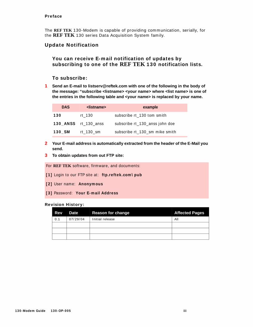
Preface
The REF TEK 130-Modem is capable of providing communication, serially, for the REF TEK 130 series Data Acquisition System family.
Update Notification
You can receive E-mail notification of updates by subscribing to one of the REF TEK 130 notification lists.
To subscribe:
1 Send an E-mail to [email protected] with one of the following in the body of the message: “subscribe <listname> <your name> where <list name> is one of the entries in the following table and <your name> is replaced by your name.
2 Your E-mail address is automatically extracted from the header of the E-Mail you send.
3 To obtain updates from out FTP site:
Revision History:
DAS <listname> example
130 rt_130 subscribe rt_130 tom smith
130_ANSS rt_130_anss subscribe rt_130_anss john doe
130_SM rt_130_sm subscribe rt_130_sm mike smith
For REF TEK software, firmware, and documents:
[1] Login to our FTP site at: ftp.reftek.com\pub
[2] User name: Anonymous
[3] Password: Your E-mail Address
Rev Date Reason for change Affected Pages0.1 07/29/04 Initial release All
130-Modem Guide 130-OP-005 iii
iv 13
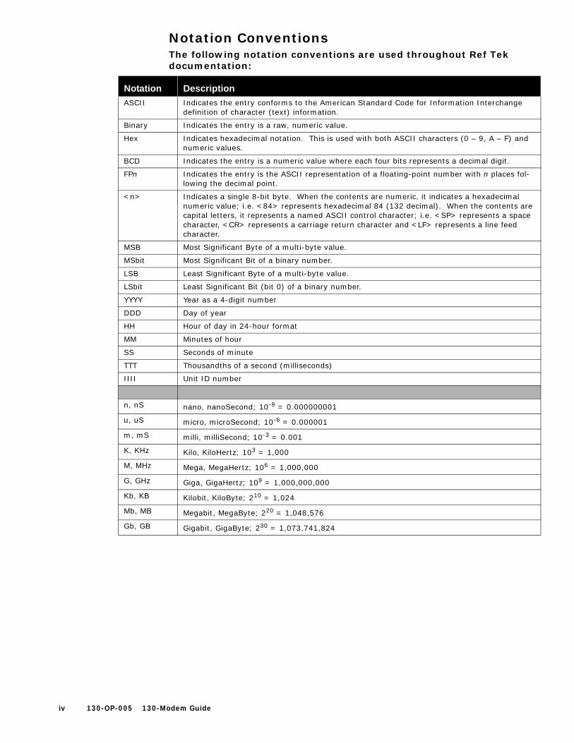
Notation ConventionsThe following notation conventions are used throughout Ref Tek documentation:
Notation DescriptionASCII Indicates the entry conforms to the American Standard Code for Information Interchange
definition of character (text) information.
Binary Indicates the entry is a raw, numeric value.
Hex Indicates hexadecimal notation. This is used with both ASCII characters (0 – 9, A – F) and numeric values.
BCD Indicates the entry is a numeric value where each four bits represents a decimal digit.
FPn Indicates the entry is the ASCII representation of a floating-point number with n places fol-lowing the decimal point.
<n> Indicates a single 8-bit byte. When the contents are numeric, it indicates a hexadecimal numeric value; i.e. <84> represents hexadecimal 84 (132 decimal). When the contents are capital letters, it represents a named ASCII control character; i.e. <SP> represents a space character, <CR> represents a carriage return character and <LF> represents a line feed character.
MSB Most Significant Byte of a multi-byte value.
MSbit Most Significant Bit of a binary number.
LSB Least Significant Byte of a multi-byte value.
LSbit Least Significant Bit (bit 0) of a binary number.
YYYY Year as a 4-digit number
DDD Day of year
HH Hour of day in 24-hour format
MM Minutes of hour
SS Seconds of minute
TTT Thousandths of a second (milliseconds)
IIII Unit ID number
n, nS nano, nanoSecond; 10-9 = 0.000000001
u, uS micro, microSecond; 10-6 = 0.000001
m, mS milli, milliSecond; 10-3 = 0.001
K, KHz Kilo, KiloHertz; 103 = 1,000
M, MHz Mega, MegaHertz; 106 = 1,000,000
G, GHz Giga, GigaHertz; 109 = 1,000,000,000
Kb, KB Kilobit, KiloByte; 210 = 1,024
Mb, MB Megabit, MegaByte; 220 = 1,048,576
Gb, GB Gigabit, GigaByte; 230 = 1,073,741,824
0-OP-005 130-Modem Guide
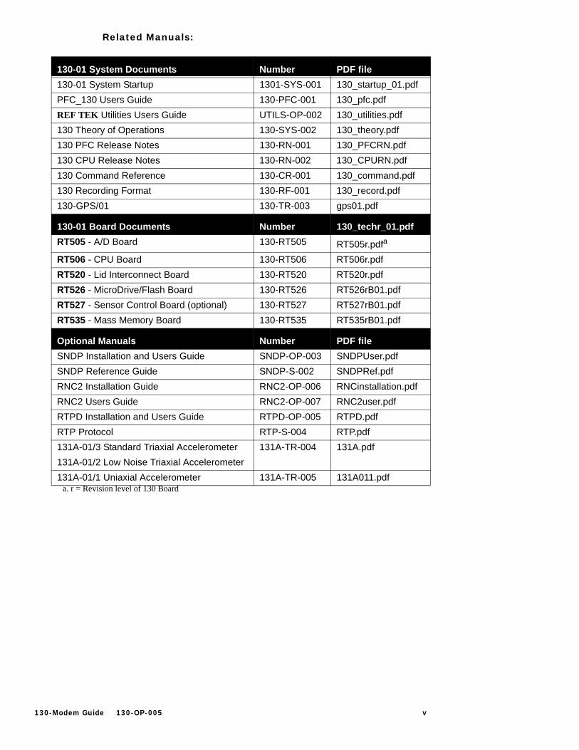
Related Manuals:
130-01 System Documents Number PDF file130-01 System Startup 1301-SYS-001 130_startup_01.pdfPFC_130 Users Guide 130-PFC-001 130_pfc.pdfREF TEK Utilities Users Guide UTILS-OP-002 130_utilities.pdf130 Theory of Operations 130-SYS-002 130_theory.pdf130 PFC Release Notes 130-RN-001 130_PFCRN.pdf130 CPU Release Notes 130-RN-002 130_CPURN.pdf130 Command Reference 130-CR-001 130_command.pdf130 Recording Format 130-RF-001 130_record.pdf130-GPS/01 130-TR-003 gps01.pdf
130-01 Board Documents Number 130_techr_01.pdfRT505 - A/D Board 130-RT505 RT505r.pdfa
RT506 - CPU Board 130-RT506 RT506r.pdfRT520 - Lid Interconnect Board 130-RT520 RT520r.pdfRT526 - MicroDrive/Flash Board 130-RT526 RT526rB01.pdfRT527 - Sensor Control Board (optional) 130-RT527 RT527rB01.pdfRT535 - Mass Memory Board 130-RT535 RT535rB01.pdf
Optional Manuals Number PDF fileSNDP Installation and Users Guide SNDP-OP-003 SNDPUser.pdfSNDP Reference Guide SNDP-S-002 SNDPRef.pdfRNC2 Installation Guide RNC2-OP-006 RNCinstallation.pdfRNC2 Users Guide RNC2-OP-007 RNC2user.pdfRTPD Installation and Users Guide RTPD-OP-005 RTPD.pdfRTP Protocol RTP-S-004 RTP.pdf131A-01/3 Standard Triaxial Accelerometer131A-01/2 Low Noise Triaxial Accelerometer
131A-TR-004 131A.pdf
131A-01/1 Uniaxial Accelerometer 131A-TR-005 131A011.pdfa. r = Revision level of 130 Board
130-Modem Guide 130-OP-005 v
vi 13
About this manual:
This 130-Modem Guide provides detailed information for the use of the 130-Modem with the REF TEK 130 DAS family.
Software Version:
Current software and documentation is available on our web site. Some early units may require hardware modifications to use the latest software. Contact REF TEK if you have any queries on the compatibility of your unit(s) and the current software release.
0-OP-005 130-Modem Guide
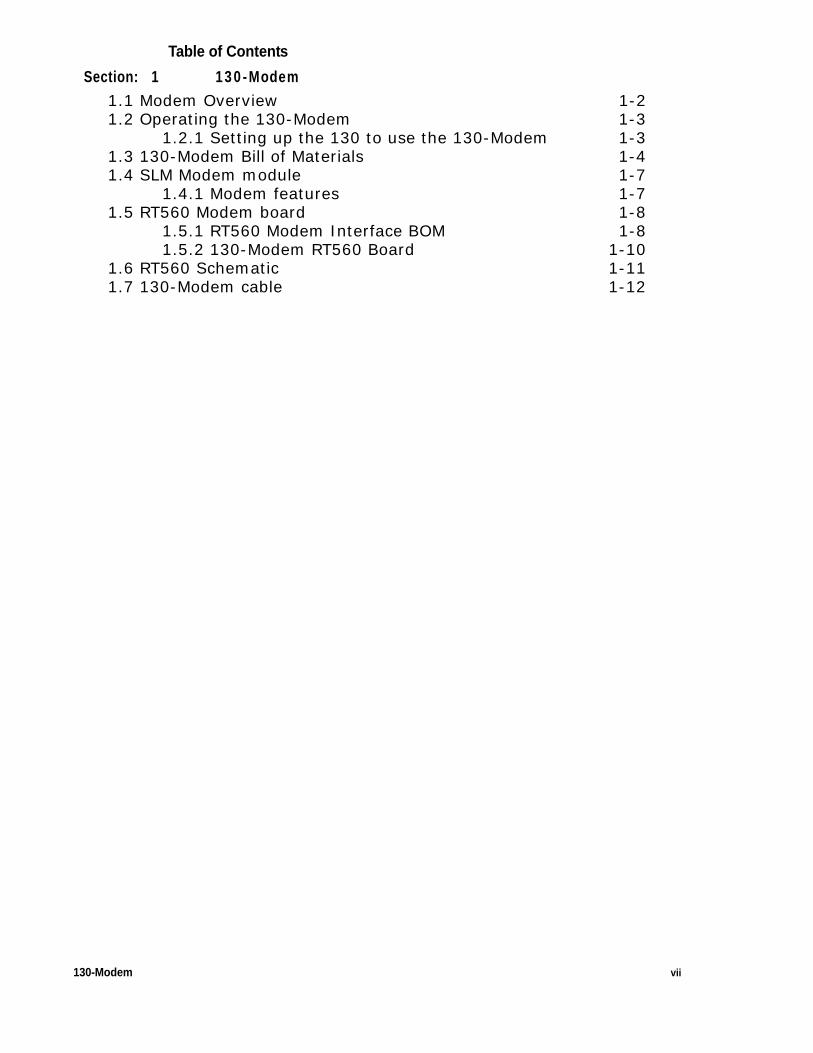
Table of Contents
Section: 1 130-Modem1.1 Modem Overview 1-21.2 Operating the 130-Modem 1-3
1.2.1 Setting up the 130 to use the 130-Modem 1-31.3 130-Modem Bill of Materials 1-41.4 SLM Modem module 1-7
1.4.1 Modem features 1-71.5 RT560 Modem board 1-8
1.5.1 RT560 Modem Interface BOM 1-81.5.2 130-Modem RT560 Board 1-10
1.6 RT560 Schematic 1-111.7 130-Modem cable 1-12
130-Modem vii

viii
130-01 System Startup
Section 1130-Modem
This Section explains the REF TEK 130-Modem when it isused with the REF TEK 130 family. The 130-Modem is anoptional external modem.
A user should be familiar with whatever REF TEK host system isin current use. Documents for other REF TEK products areavailable on request.
130-Modem Guide 130-OPS-005 1-1
Modem Overview
1.1 Modem Overview
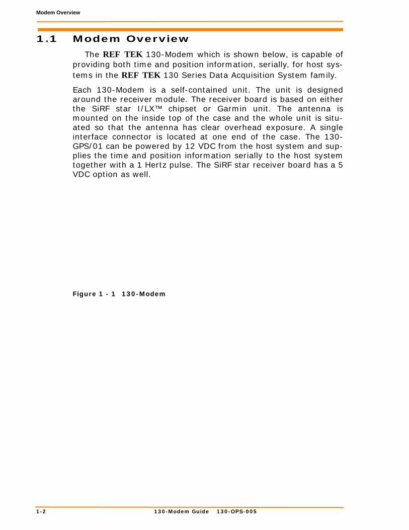
The REF TEK 130-Modem which is shown below, is capable ofproviding both time and position information, serially, for host sys-tems in the REF TEK 130 Series Data Acquisition System family.
Each 130-Modem is a self-contained unit. The unit is designedaround the receiver module. The receiver board is based on eitherthe SiRF star I/LX™ chipset or Garmin unit. The antenna ismounted on the inside top of the case and the whole unit is situ-ated so that the antenna has clear overhead exposure. A singleinterface connector is located at one end of the case. The 130-GPS/01 can be powered by 12 VDC from the host system and sup-plies the time and position information serially to the host systemtogether with a 1 Hertz pulse. The SiRF star receiver board has a 5VDC option as well.
Figure 1 - 1 130-Modem
1-2 130-Modem Guide 130-OPS-005
Operating the 130-Modem
1.2 Operating the 130-ModemThis section provides general procedures for setting up and
operating the REF TEK 130-Modem.
1.2.1 Setting up the 130 to use the 130-Modem
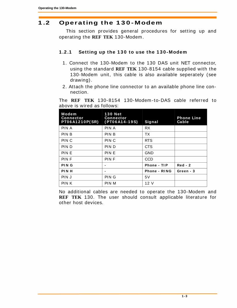
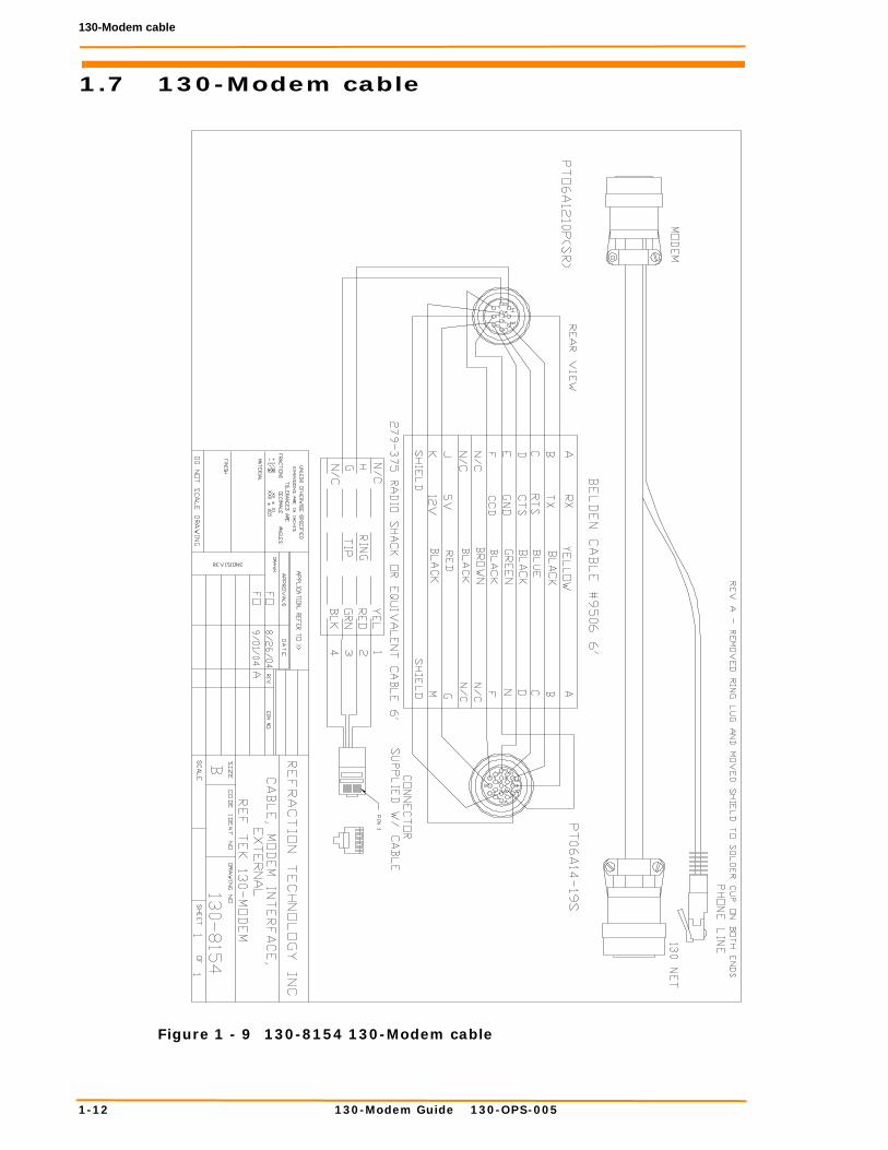
1. Connect the 130-Modem to the 130 DAS unit NET connector,using the standard REF TEK 130-8154 cable supplied with the130-Modem unit, this cable is also available seperately (seedrawing).
2. Attach the phone line connector to an available phone line con-nection.
The REF TEK 130-8154 130-Modem-to-DAS cable referred toabove is wired as follows:
No additional cables are needed to operate the 130-Modem andREF TEK 130. The user should consult applicable literature forother host devices.
Modem Connector PT06A1210P(SR)
130 Net Connector (PT06A14-19S) Signal
Phone LineCable
PIN A PIN A RX
PIN B PIN B TX
PIN C PIN C RTS
PIN D PIN D CTS
PIN E PIN E GND
PIN F PIN F CCD
PIN G - Phone - TIP Red - 2
PIN H - Phone - RING Green - 3
PIN J PIN G 5V
PIN K PIN M 12 V
1-3
130-Modem Bill of Materials
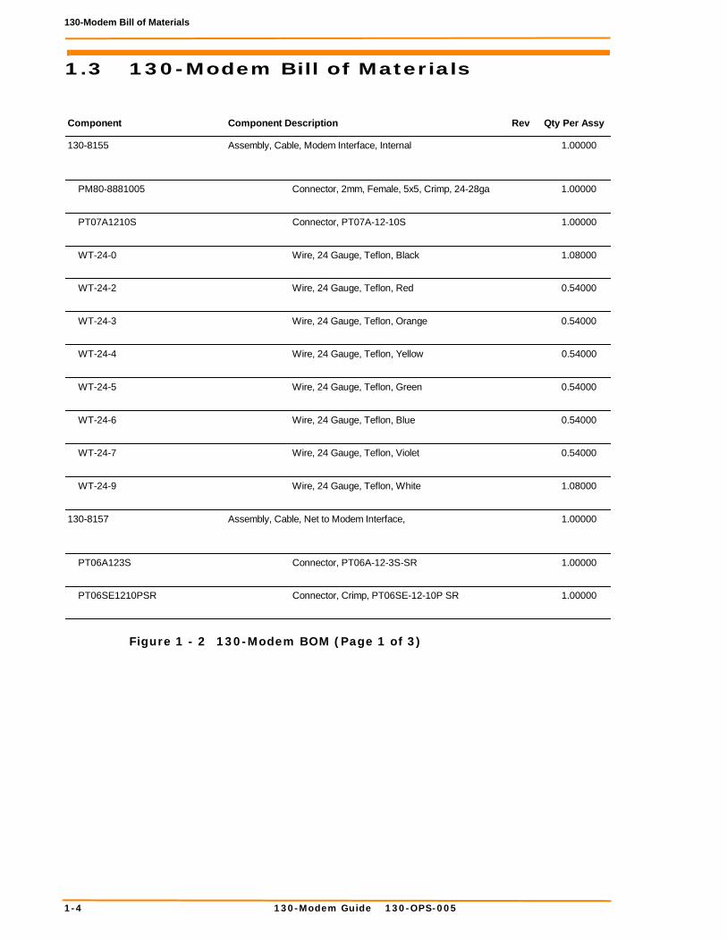
1.3 130-Modem Bill of Materials
Figure 1 - 2 130-Modem BOM (Page 1 of 3)
Qty Per AssyRevComponent DescriptionComponent
130-8155 Assembly, Cable, Modem Interface, Internal 1.00000
PM80-8881005 Connector, 2mm, Female, 5x5, Crimp, 24-28ga 1.00000
PT07A1210S Connector, PT07A-12-10S 1.00000
WT-24-0 Wire, 24 Gauge, Teflon, Black 1.08000
WT-24-2 Wire, 24 Gauge, Teflon, Red 0.54000
WT-24-3 Wire, 24 Gauge, Teflon, Orange 0.54000
WT-24-4 Wire, 24 Gauge, Teflon, Yellow 0.54000
WT-24-5 Wire, 24 Gauge, Teflon, Green 0.54000
WT-24-6 Wire, 24 Gauge, Teflon, Blue 0.54000
WT-24-7 Wire, 24 Gauge, Teflon, Violet 0.54000
WT-24-9 Wire, 24 Gauge, Teflon, White 1.08000
130-8157 Assembly, Cable, Net to Modem Interface, 1.00000
PT06A123S Connector, PT06A-12-3S-SR 1.00000
PT06SE1210PSR Connector, Crimp, PT06SE-12-10P SR 1.00000
1-4 130-Modem Guide 130-OPS-005
130-Modem Bill of Materials
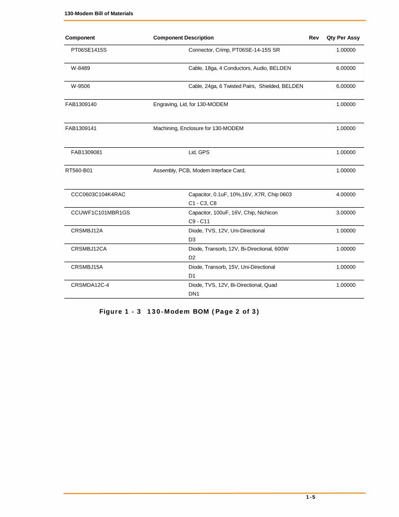
Figure 1 - 3 130-Modem BOM (Page 2 of 3)
Qty Per AssyRevComponent DescriptionComponent
PT06SE1415S Connector, Crimp, PT06SE-14-15S SR 1.00000
W-8489 Cable, 18ga, 4 Conductors, Audio, BELDEN 6.00000
W-9506 Cable, 24ga, 6 Twisted Pairs, Shielded, BELDEN 6.00000
FAB1309140 Engraving, Lid, for 130-MODEM 1.00000
FAB1309141 Machining, Enclosure for 130-MODEM 1.00000
FAB1309081 Lid, GPS 1.00000
RT560-B01 Assembly, PCB, Modem Interface Card, 1.00000
CCC0603C104K4RAC Capacitor, 0.1uF, 10%,16V, X7R, Chip 0603 4.00000
C1 - C3, C8
CCUWF1C101MBR1GS Capacitor, 100uF, 16V, Chip, Nichicon 3.00000
C9 - C11
CRSMBJ12A Diode, TVS, 12V, Uni-Directional 1.00000
D3
CRSMBJ12CA Diode, Transorb, 12V, Bi-Directional, 600W 1.00000
D2
CRSMBJ15A Diode, Transorb, 15V, Uni-Directional 1.00000
D1
CRSMDA12C-4 Diode, TVS, 12V, Bi-Directional, Quad 1.00000
DN1
1-5
130-Modem Bill of Materials
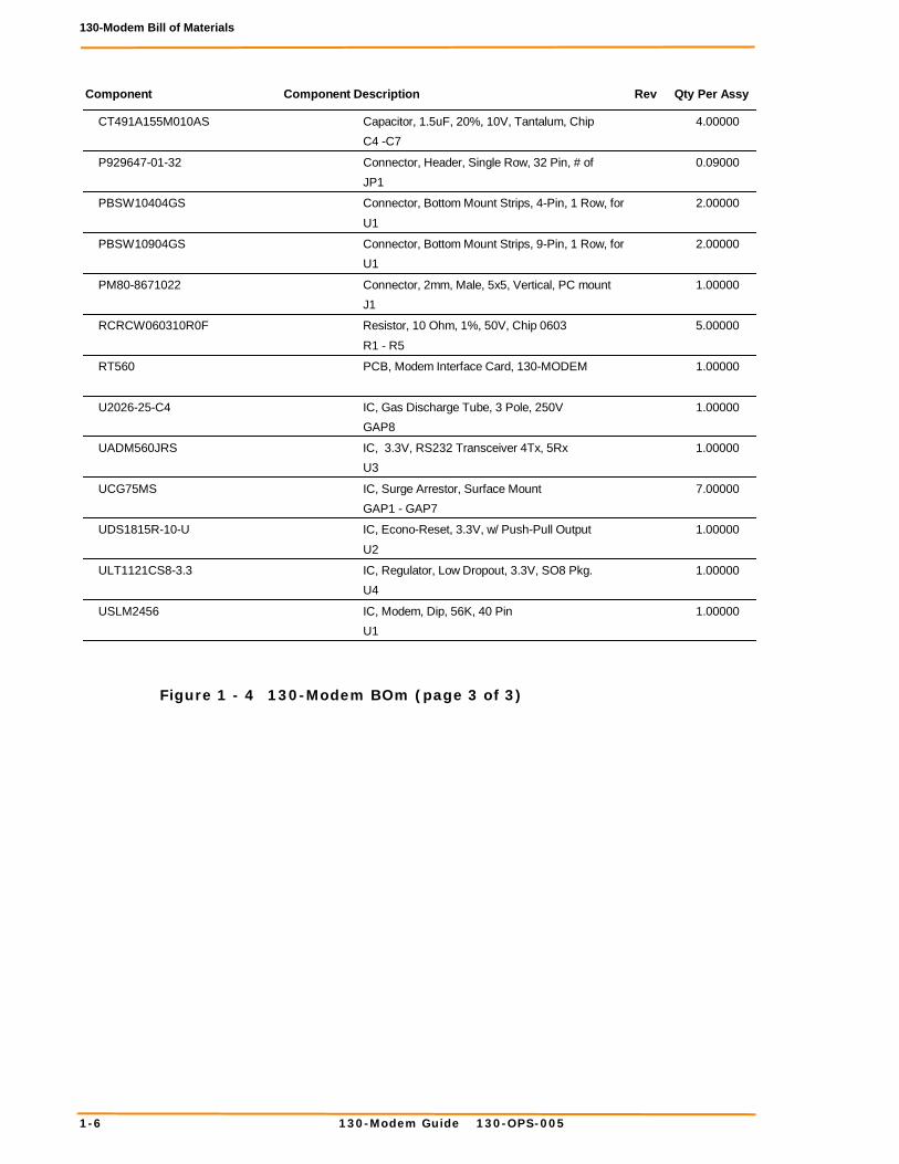
Figure 1 - 4 130-Modem BOm (page 3 of 3)
Qty Per AssyRevComponent DescriptionComponent
CT491A155M010AS Capacitor, 1.5uF, 20%, 10V, Tantalum, Chip 4.00000
C4 -C7
P929647-01-32 Connector, Header, Single Row, 32 Pin, # of 0.09000
JP1
PBSW10404GS Connector, Bottom Mount Strips, 4-Pin, 1 Row, for 2.00000
U1
PBSW10904GS Connector, Bottom Mount Strips, 9-Pin, 1 Row, for 2.00000
U1
PM80-8671022 Connector, 2mm, Male, 5x5, Vertical, PC mount 1.00000
J1
RCRCW060310R0F Resistor, 10 Ohm, 1%, 50V, Chip 0603 5.00000
R1 - R5
RT560 PCB, Modem Interface Card, 130-MODEM 1.00000
U2026-25-C4 IC, Gas Discharge Tube, 3 Pole, 250V 1.00000
GAP8
UADM560JRS IC, 3.3V, RS232 Transceiver 4Tx, 5Rx 1.00000
U3
UCG75MS IC, Surge Arrestor, Surface Mount 7.00000
GAP1 - GAP7
UDS1815R-10-U IC, Econo-Reset, 3.3V, w/ Push-Pull Output 1.00000
U2
ULT1121CS8-3.3 IC, Regulator, Low Dropout, 3.3V, SO8 Pkg. 1.00000
U4
USLM2456 IC, Modem, Dip, 56K, 40 Pin 1.00000
U1
1-6 130-Modem Guide 130-OPS-005
SLM Modem module
1.4 SLM Modem moduleThe SLM2456 modem module is used in the 130-Modem and as
the internal modem for the 130-SM. The SLM2456 is a complete,modem module that is based on the Si2456 chipset. The Si2456 isan ITU-V.90 compliant, 56 kbps modem chipset with integrateddirect access arrangement (also called DAA it includes parallelphone detect, over-current detection and global PTT compliance).This provides a programmable line interface to meet global tele-phone line requirements. It is a single design that includes a DSPdata pump, a modem controller, on-chip RAM and ROM, an analogfront end (AFE) a DAA, and analog output.
1.4.1 Modem features
The SLM2456 accepts standard modem AT commands and providesconnect rates up to 56/33.6/14.4 kbps full-duplex over the PublicSwitched Telephone Network (PTN). It also features a complete setof modem protocols including all ITU-T standard formats up to 56kbps.
Note: This material is part of the Silicon Laboratories® Si2456/33/14 data sheet document revision 1.0. See the Si2456/33/14 Users Guide (“AN70:Si245/Si2433/Si2414/Si2403 Modem Designer’s Guide) for detailed feature explanations.
1-7
RT560 Modem board
1.5 RT560 Modem board
1.5.1 RT560 Modem Interface BOM
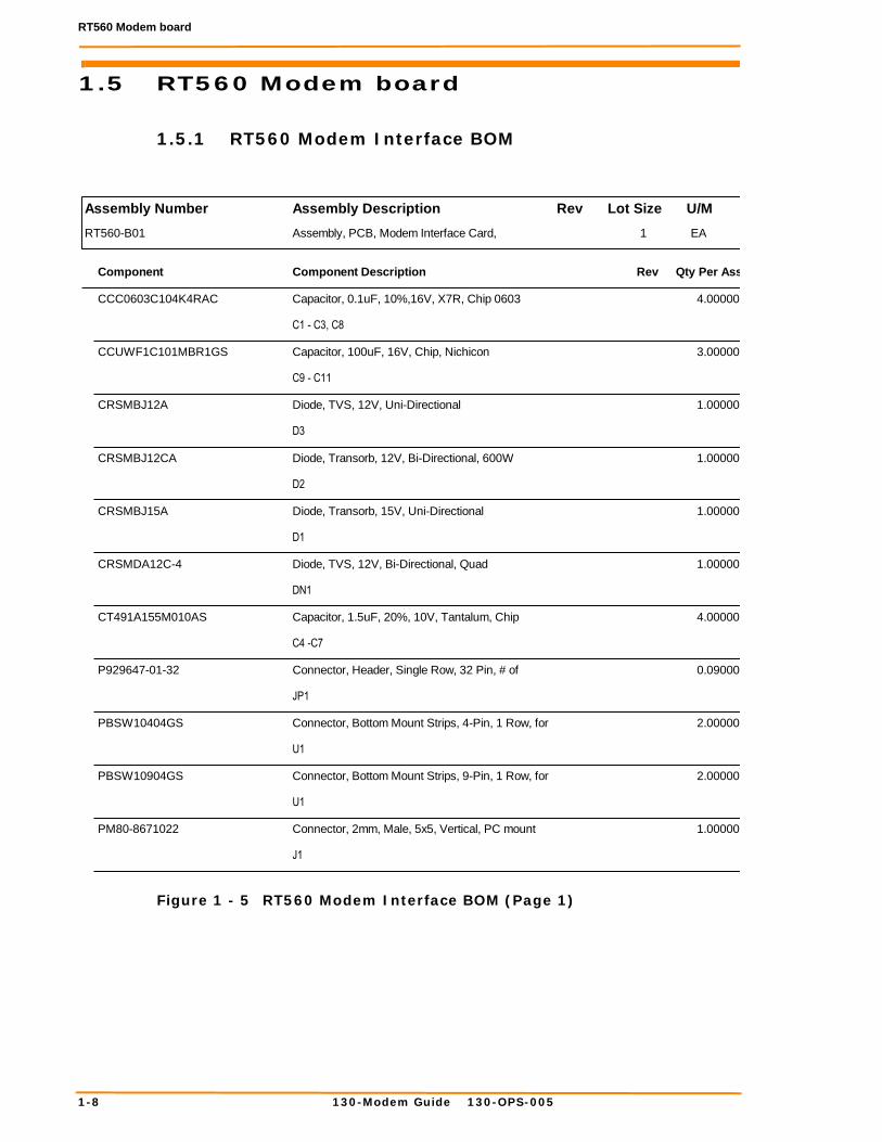
Figure 1 - 5 RT560 Modem Interface BOM (Page 1)
U/M
EA
RevAssembly Description
Assembly, PCB, Modem Interface Card,
Assembly Number
RT560-B01
Qty Per AssRevComponent DescriptionComponent
1
Lot Size
CCC0603C104K4RAC Capacitor, 0.1uF, 10%,16V, X7R, Chip 0603 4.00000
C1 - C3, C8
CCUWF1C101MBR1GS Capacitor, 100uF, 16V, Chip, Nichicon 3.00000
C9 - C11
CRSMBJ12A Diode, TVS, 12V, Uni-Directional 1.00000
D3
CRSMBJ12CA Diode, Transorb, 12V, Bi-Directional, 600W 1.00000
D2
CRSMBJ15A Diode, Transorb, 15V, Uni-Directional 1.00000
D1
CRSMDA12C-4 Diode, TVS, 12V, Bi-Directional, Quad 1.00000
DN1
CT491A155M010AS Capacitor, 1.5uF, 20%, 10V, Tantalum, Chip 4.00000
C4 -C7
P929647-01-32 Connector, Header, Single Row, 32 Pin, # of 0.09000
JP1
PBSW10404GS Connector, Bottom Mount Strips, 4-Pin, 1 Row, for 2.00000
U1
PBSW10904GS Connector, Bottom Mount Strips, 9-Pin, 1 Row, for 2.00000
U1
PM80-8671022 Connector, 2mm, Male, 5x5, Vertical, PC mount 1.00000
J1
1-8 130-Modem Guide 130-OPS-005
RT560 Modem board
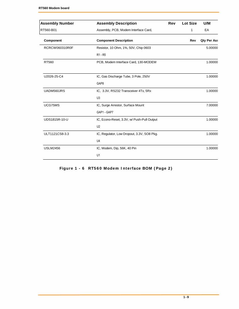
Figure 1 - 6 RT560 Modem Interface BOM (Page 2)
U/M
EA
RevAssembly Description
Assembly, PCB, Modem Interface Card,
Assembly Number
RT560-B01
Qty Per AssRevComponent DescriptionComponent
1
Lot Size
RCRCW060310R0F Resistor, 10 Ohm, 1%, 50V, Chip 0603 5.00000
R1 - R5
RT560 PCB, Modem Interface Card, 130-MODEM 1.00000
U2026-25-C4 IC, Gas Discharge Tube, 3 Pole, 250V 1.00000
GAP8
UADM560JRS IC, 3.3V, RS232 Transceiver 4Tx, 5Rx 1.00000
U3
UCG75MS IC, Surge Arrestor, Surface Mount 7.00000
GAP1 - GAP7
UDS1815R-10-U IC, Econo-Reset, 3.3V, w/ Push-Pull Output 1.00000
U2
ULT1121CS8-3.3 IC, Regulator, Low Dropout, 3.3V, SO8 Pkg. 1.00000
U4
USLM2456 IC, Modem, Dip, 56K, 40 Pin 1.00000
U1
1-9
RT560 Modem board
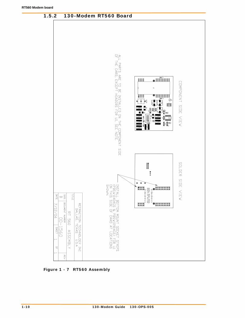
1.5.2 130-Modem RT560 Board
Figure 1 - 7 RT560 Assembly
1-10 130-Modem Guide 130-OPS-005
RT560 Schematic
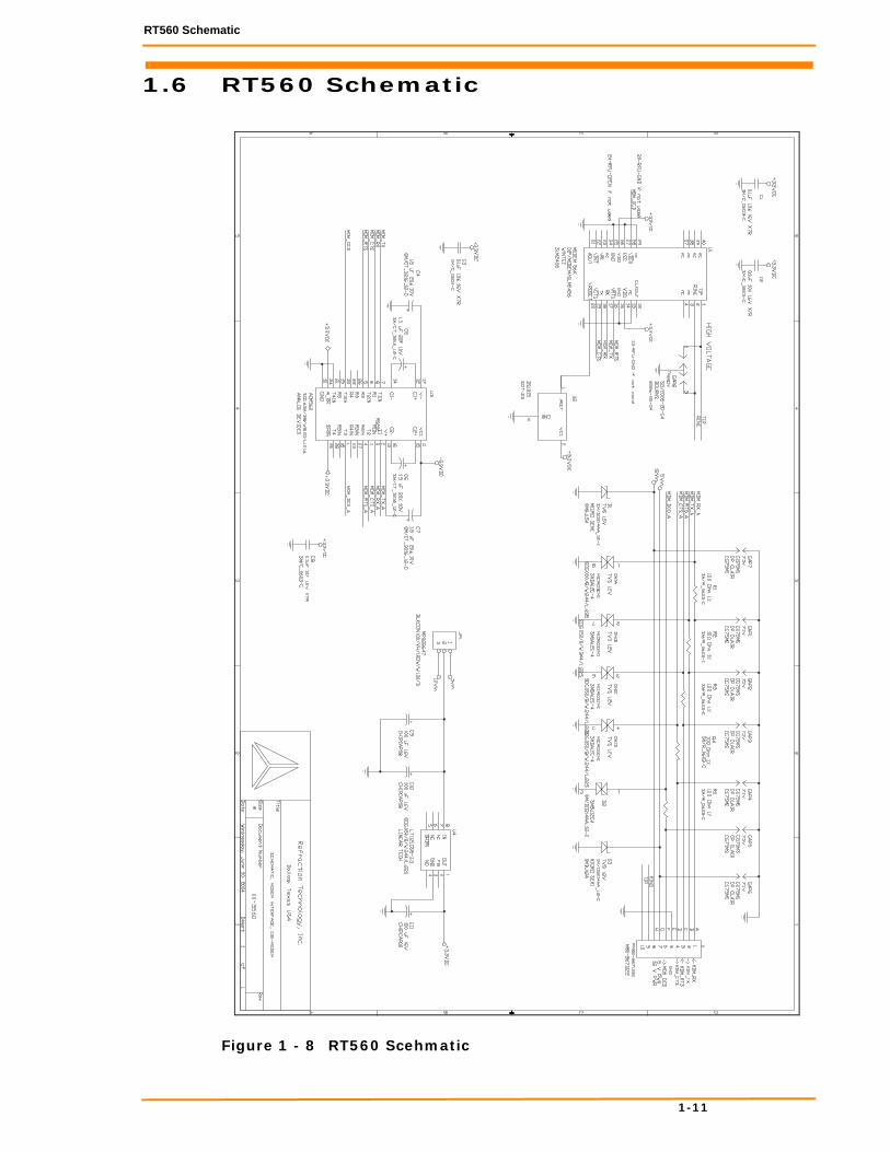
1.6 RT560 Schematic
Figure 1 - 8 RT560 Scehmatic
1-11
130-Modem cable
1.7 130-Modem cable
Figure 1 - 9 130-8154 130-Modem cable
1-12 130-Modem Guide 130-OPS-005
Si2456/Si2433/Si2414
22 Rev. 1.0
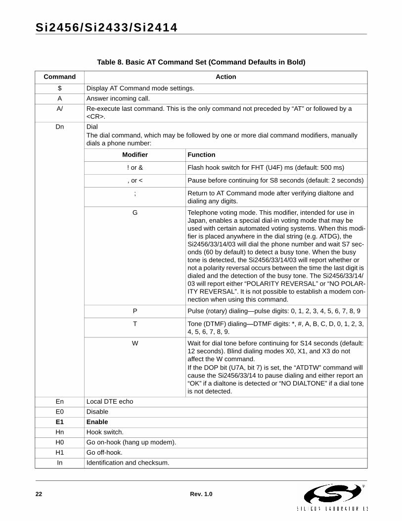
Table 8. Basic AT Command Set (Command Defaults in Bold)
Command Action$ Display AT Command mode settings.A Answer incoming call.A/ Re-execute last command. This is the only command not preceded by “AT” or followed by a
<CR>.Dn Dial
The dial command, which may be followed by one or more dial command modifiers, manually dials a phone number:
Modifier Function
! or & Flash hook switch for FHT (U4F) ms (default: 500 ms)
, or < Pause before continuing for S8 seconds (default: 2 seconds)
; Return to AT Command mode after verifying dialtone and dialing any digits.
G Telephone voting mode. This modifier, intended for use in Japan, enables a special dial-in voting mode that may be used with certain automated voting systems. When this modi-fier is placed anywhere in the dial string (e.g. ATDG), the Si2456/33/14/03 will dial the phone number and wait S7 sec-onds (60 by default) to detect a busy tone. When the busy tone is detected, the Si2456/33/14/03 will report whether or not a polarity reversal occurs between the time the last digit is dialed and the detection of the busy tone. The Si2456/33/14/03 will report either “POLARITY REVERSAL” or “NO POLAR-ITY REVERSAL”. It is not possible to establish a modem con-nection when using this command.
P Pulse (rotary) dialing—pulse digits: 0, 1, 2, 3, 4, 5, 6, 7, 8, 9
T Tone (DTMF) dialing—DTMF digits: *, #, A, B, C, D, 0, 1, 2, 3, 4, 5, 6, 7, 8, 9.
W Wait for dial tone before continuing for S14 seconds (default: 12 seconds). Blind dialing modes X0, X1, and X3 do not affect the W command.If the DOP bit (U7A, bit 7) is set, the “ATDTW” command will cause the Si2456/33/14 to pause dialing and either report an “OK” if a dialtone is detected or “NO DIALTONE” if a dial tone is not detected.
En Local DTE echoE0 DisableE1 EnableHn Hook switch.H0 Go on-hook (hang up modem).H1 Go off-hook.In Identification and checksum.
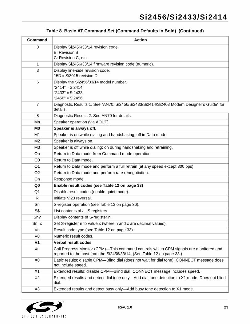
Si2456/Si2433/Si2414
Rev. 1.0 23
I0 Display Si2456/33/14 revision code.B: Revision BC: Revision C, etc.
I1 Display Si2456/33/14 firmware revision code (numeric).I3 Display line-side revision code.
15D = Si3015 revision DI6 Display the Si2456/33/14 model number.
“2414” = Si2414“2433” = Si2433“2456” = Si2456
I7 Diagnostic Results 1. See “AN70: Si2456/Si2433/Si2414/Si2403 Modem Designer’s Guide” for details.
I8 Diagnostic Results 2. See AN70 for details.Mn Speaker operation (via AOUT).M0 Speaker is always off.M1 Speaker is on while dialing and handshaking; off in Data mode.M2 Speaker is always on.M3 Speaker is off while dialing; on during handshaking and retraining.On Return to Data mode from Command mode operation.O0 Return to Data mode.O1 Return to Data mode and perform a full retrain (at any speed except 300 bps).O2 Return to Data mode and perform rate renegotiation.Qn Response mode.Q0 Enable result codes (see Table 12 on page 33)Q1 Disable result codes (enable quiet mode).R Initiate V.23 reversal.Sn S-register operation (see Table 13 on page 36).S$ List contents of all S registers.Sn? Display contents of S-register n.Sn=x Set S-register n to value x (where n and x are decimal values).Vn Result code type (see Table 12 on page 33).V0 Numeric result codes.V1 Verbal result codesXn Call Progress Monitor (CPM)—This command controls which CPM signals are monitored and
reported to the host from the Si2456/33/14. (See Table 12 on page 33.)X0 Basic results; disable CPM—Blind dial (does not wait for dial tone). CONNECT message does
not include speed.X1 Extended results; disable CPM—Blind dial. CONNECT message includes speed.X2 Extended results and detect dial tone only—Add dial tone detection to X1 mode. Does not blind
dial.X3 Extended results and detect busy only—Add busy tone detection to X1 mode.
Table 8. Basic AT Command Set (Command Defaults in Bold) (Continued)
Command Action
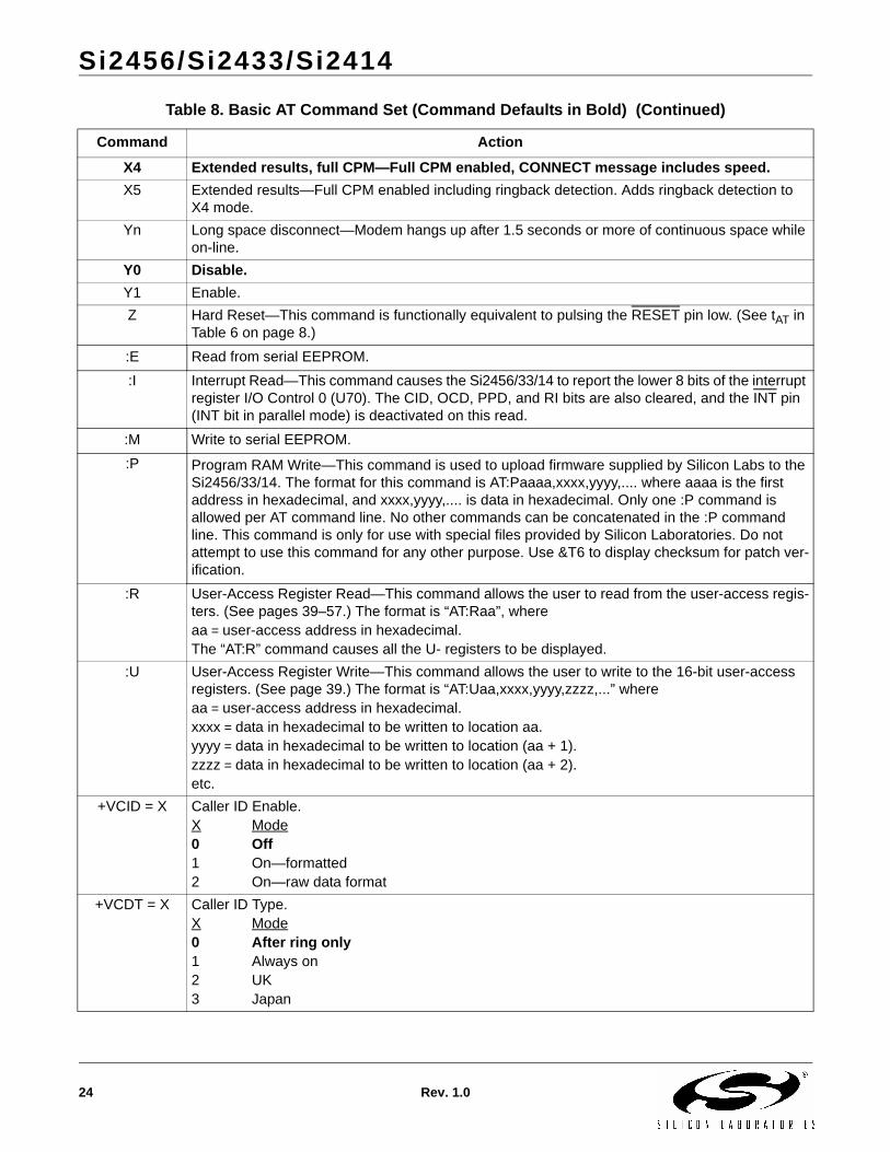
Si2456/Si2433/Si2414
24 Rev. 1.0
X4 Extended results, full CPM—Full CPM enabled, CONNECT message includes speed.X5 Extended results—Full CPM enabled including ringback detection. Adds ringback detection to
X4 mode.Yn Long space disconnect—Modem hangs up after 1.5 seconds or more of continuous space while
on-line.Y0 Disable.Y1 Enable.Z Hard Reset—This command is functionally equivalent to pulsing the RESET pin low. (See tAT in
Table 6 on page 8.):E Read from serial EEPROM.:I Interrupt Read—This command causes the Si2456/33/14 to report the lower 8 bits of the interrupt
register I/O Control 0 (U70). The CID, OCD, PPD, and RI bits are also cleared, and the INT pin (INT bit in parallel mode) is deactivated on this read.
:M Write to serial EEPROM.:P Program RAM Write—This command is used to upload firmware supplied by Silicon Labs to the
Si2456/33/14. The format for this command is AT:Paaaa,xxxx,yyyy,.... where aaaa is the first address in hexadecimal, and xxxx,yyyy,.... is data in hexadecimal. Only one :P command is allowed per AT command line. No other commands can be concatenated in the :P command line. This command is only for use with special files provided by Silicon Laboratories. Do not attempt to use this command for any other purpose. Use &T6 to display checksum for patch ver-ification.
:R User-Access Register Read—This command allows the user to read from the user-access regis-ters. (See pages 39–57.) The format is “AT:Raa”, whereaa = user-access address in hexadecimal.The “AT:R” command causes all the U- registers to be displayed.
:U User-Access Register Write—This command allows the user to write to the 16-bit user-access registers. (See page 39.) The format is “AT:Uaa,xxxx,yyyy,zzzz,...” whereaa = user-access address in hexadecimal.xxxx = data in hexadecimal to be written to location aa.yyyy = data in hexadecimal to be written to location (aa + 1).zzzz = data in hexadecimal to be written to location (aa + 2).etc.
+VCID = X Caller ID Enable.X Mode0 Off1 On—formatted2 On—raw data format
+VCDT = X Caller ID Type.X Mode0 After ring only1 Always on2 UK3 Japan
Table 8. Basic AT Command Set (Command Defaults in Bold) (Continued)
Command Action
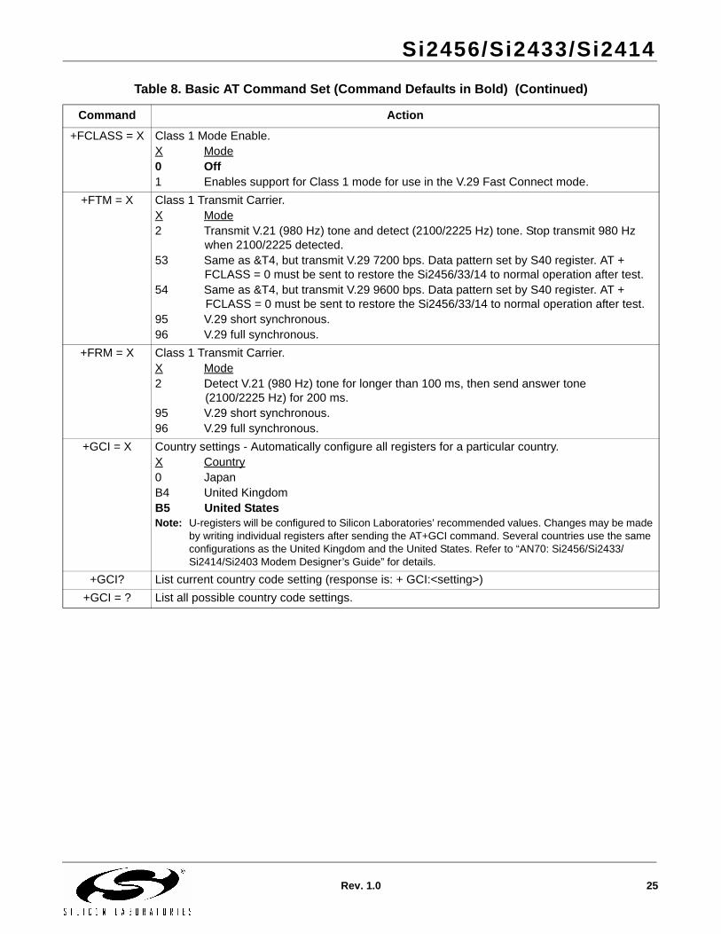
Si2456/Si2433/Si2414
Rev. 1.0 25
+FCLASS = X Class 1 Mode Enable.X Mode0 Off1 Enables support for Class 1 mode for use in the V.29 Fast Connect mode.
+FTM = X Class 1 Transmit Carrier.X Mode2 Transmit V.21 (980 Hz) tone and detect (2100/2225 Hz) tone. Stop transmit 980 Hz
when 2100/2225 detected.53 Same as &T4, but transmit V.29 7200 bps. Data pattern set by S40 register. AT +
FCLASS = 0 must be sent to restore the Si2456/33/14 to normal operation after test.54 Same as &T4, but transmit V.29 9600 bps. Data pattern set by S40 register. AT +
FCLASS = 0 must be sent to restore the Si2456/33/14 to normal operation after test.95 V.29 short synchronous.96 V.29 full synchronous.
+FRM = X Class 1 Transmit Carrier.X Mode2 Detect V.21 (980 Hz) tone for longer than 100 ms, then send answer tone
(2100/2225 Hz) for 200 ms.95 V.29 short synchronous.96 V.29 full synchronous.
+GCI = X Country settings - Automatically configure all registers for a particular country.X Country0 JapanB4 United KingdomB5 United StatesNote: U-registers will be configured to Silicon Laboratories’ recommended values. Changes may be made
by writing individual registers after sending the AT+GCI command. Several countries use the same configurations as the United Kingdom and the United States. Refer to “AN70: Si2456/Si2433/Si2414/Si2403 Modem Designer’s Guide” for details.
+GCI? List current country code setting (response is: + GCI:<setting>)+GCI = ? List all possible country code settings.
Table 8. Basic AT Command Set (Command Defaults in Bold) (Continued)
Command Action
Si2456/Si2433/Si2414
26 Rev. 1.0
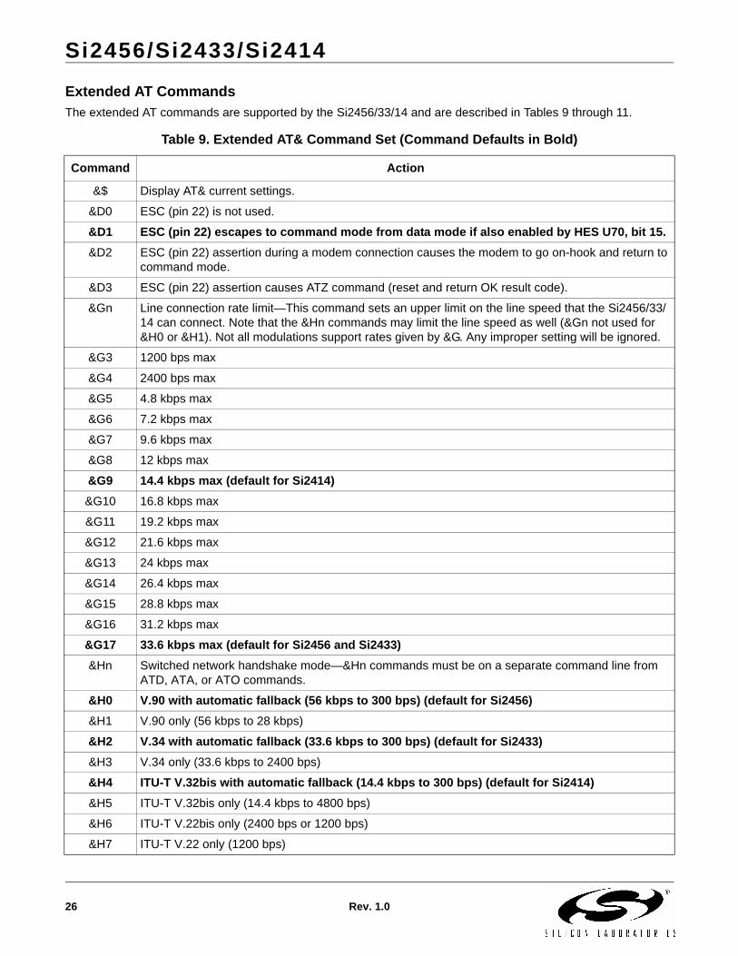
Extended AT CommandsThe extended AT commands are supported by the Si2456/33/14 and are described in Tables 9 through 11.
Table 9. Extended AT& Command Set (Command Defaults in Bold)
Command Action
&$ Display AT& current settings.
&D0 ESC (pin 22) is not used.
&D1 ESC (pin 22) escapes to command mode from data mode if also enabled by HES U70, bit 15.&D2 ESC (pin 22) assertion during a modem connection causes the modem to go on-hook and return to
command mode.
&D3 ESC (pin 22) assertion causes ATZ command (reset and return OK result code).
&Gn Line connection rate limit—This command sets an upper limit on the line speed that the Si2456/33/14 can connect. Note that the &Hn commands may limit the line speed as well (&Gn not used for &H0 or &H1). Not all modulations support rates given by &G. Any improper setting will be ignored.
&G3 1200 bps max
&G4 2400 bps max
&G5 4.8 kbps max
&G6 7.2 kbps max
&G7 9.6 kbps max
&G8 12 kbps max
&G9 14.4 kbps max (default for Si2414)&G10 16.8 kbps max
&G11 19.2 kbps max
&G12 21.6 kbps max
&G13 24 kbps max
&G14 26.4 kbps max
&G15 28.8 kbps max
&G16 31.2 kbps max
&G17 33.6 kbps max (default for Si2456 and Si2433)&Hn Switched network handshake mode—&Hn commands must be on a separate command line from
ATD, ATA, or ATO commands.
&H0 V.90 with automatic fallback (56 kbps to 300 bps) (default for Si2456)&H1 V.90 only (56 kbps to 28 kbps)
&H2 V.34 with automatic fallback (33.6 kbps to 300 bps) (default for Si2433)&H3 V.34 only (33.6 kbps to 2400 bps)
&H4 ITU-T V.32bis with automatic fallback (14.4 kbps to 300 bps) (default for Si2414)&H5 ITU-T V.32bis only (14.4 kbps to 4800 bps)
&H6 ITU-T V.22bis only (2400 bps or 1200 bps)
&H7 ITU-T V.22 only (1200 bps)
Si2456/Si2433/Si2414
Rev. 1.0 27
&H8 Bell 212 only (1200 bps)
&H9 Bell 103 only (300 bps)
&H10 ITU-T V.21 only (300 bps)
&H11 V.23 (1200/75 bps)
&Pn Japan pulse dialing
&P0 Configure Si2456/33/14 for 10 pulse-per-second pulse dialing. For Japan.
&P1 Configure Si2456/33/14 for 20 pulse-per-second pulse dialing. For Japan.
&Tn Test Mode
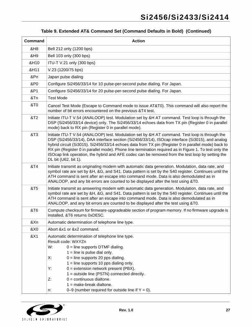
&T0 Cancel Test Mode (Escape to Command mode to issue AT&T0). This command will also report the number of bit errors encountered on the previous &T4 test.
&T2 Initiate ITU-T V.54 (ANALOOP) test. Modulation set by &H AT command. Test loop is through the DSP (Si2456/33/14 device) only. The Si2456/33/14 echoes data from TX pin (Register 0 in parallel mode) back to RX pin (Register 0 in parallel mode).
&T3 Initiate ITU-T V.54 (ANALOOP) test. Modulation set by &H AT command. Test loop is through the DSP (Si2456/33/14), DAA interface section (Si2456/33/14), ISOcap interface (Si3015), and analog hybrid circuit (Si3015). Si2456/33/14 echoes data from TX pin (Register 0 in parallel mode) back to RX pin (Register 0 in parallel mode). Phone line termination required as in Figure 1. To test only the ISOcap link operation, the hybrid and AFE codec can be removed from the test loop by setting the DL bit (U62, bit 1).
&T4 Initiate transmit as originating modem with automatic data generation. Modulation, data rate, and symbol rate are set by &H, &G, and S41. Data pattern is set by the S40 register. Continues until the ATH command is sent after an escape into command mode. Data is also demodulated as inANALOOP, and any bit errors are counted to be displayed after the test using &T0.
&T5 Initiate transmit as answering modem with automatic data generation. Modulation, data rate, and symbol rate are set by &H, &G, and S41. Data pattern is set by the S40 register. Continues until the ATH command is sent after an escape into command mode. Data is also demodulated as inANALOOP, and any bit errors are counted to be displayed after the test using &T0.
&T6 Compute checksum for firmware-upgradeable section of program memory. If no firmware upgrade is installed, &T6 returns 0xDE5C.
&Xn Automatic determination of telephone line type.
&X0 Abort &x1 or &x2 command.
&X1 Automatic determination of telephone line type.Result code: WXYZnW: 0 = line supports DTMF dialing.
1 = line is pulse dial only.X: 0 = line supports 20 pps dialing.
1 = line supports 10 pps dialing only.Y: 0 = extension network present (PBX).
1 = outside line (PSTN) connected directly.Z: 0 = continuous dialtone.
1 = make-break dialtone.n: 0–9 (number required for outside line if Y = 0).
Table 9. Extended AT& Command Set (Command Defaults in Bold) (Continued)
Command Action
Si2456/Si2433/Si2414
28 Rev. 1.0
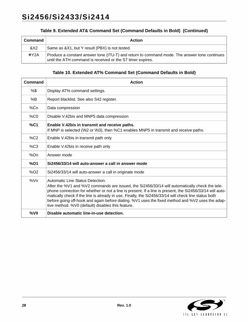
&X2 Same as &X1, but Y result (PBX) is not tested.
*Y2A Produce a constant answer tone (ITU-T) and return to command mode. The answer tone continues until the ATH command is received or the S7 timer expires.
Table 10. Extended AT% Command Set (Command Defaults in Bold)
Command Action
%$ Display AT% command settings.
%B Report blacklist. See also S42 register.
%Cn Data compression
%C0 Disable V.42bis and MNP5 data compression
%C1 Enable V.42bis in transmit and receive paths.If MNP is selected (\N2 or \N3), then %C1 enables MNP5 in transmit and receive paths.
%C2 Enable V.42bis in transmit path only
%C3 Enable V.42bis in receive path only
%On Answer mode
%O1 Si2456/33/14 will auto-answer a call in answer mode
%O2 Si2456/33/14 will auto-answer a call in originate mode
%Vn Automatic Line Status Detection.After the %V1 and %V2 commands are issued, the Si2456/33/14 will automatically check the tele-phone connection for whether or not a line is present. If a line is present, the Si2456/33/14 will auto-matically check if the line is already in use. Finally, the Si2456/33/14 will check line status both before going off-hook and again before dialing. %V1 uses the fixed method and %V2 uses the adap-tive method. %V0 (default) disables this feature.
%V0 Disable automatic line-in-use detection.
Table 9. Extended AT& Command Set (Command Defaults in Bold) (Continued)
Command Action
Si2456/Si2433/Si2414
Rev. 1.0 29
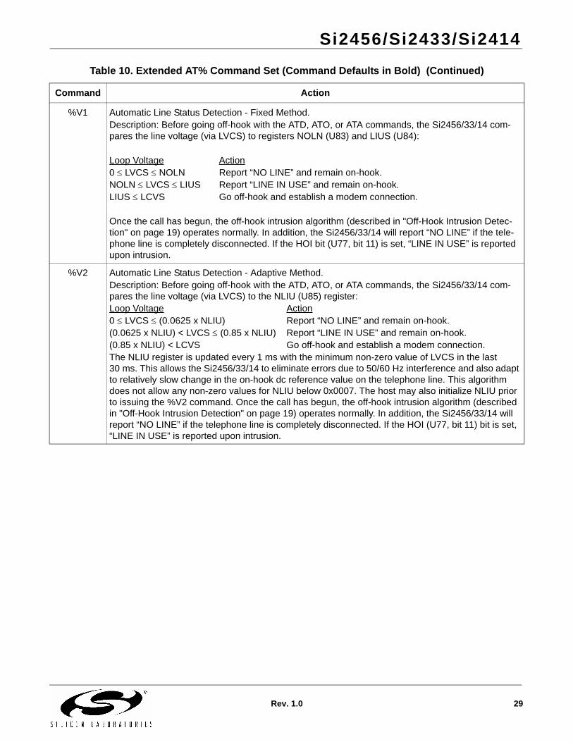
%V1 Automatic Line Status Detection - Fixed Method.Description: Before going off-hook with the ATD, ATO, or ATA commands, the Si2456/33/14 com-pares the line voltage (via LVCS) to registers NOLN (U83) and LIUS (U84):
Loop Voltage Action0 ≤ LVCS ≤ NOLN Report “NO LINE” and remain on-hook.NOLN ≤ LVCS ≤ LIUS Report “LINE IN USE” and remain on-hook.LIUS ≤ LCVS Go off-hook and establish a modem connection.
Once the call has begun, the off-hook intrusion algorithm (described in "Off-Hook Intrusion Detec-tion" on page 19) operates normally. In addition, the Si2456/33/14 will report “NO LINE” if the tele-phone line is completely disconnected. If the HOI bit (U77, bit 11) is set, “LINE IN USE” is reported upon intrusion.
%V2 Automatic Line Status Detection - Adaptive Method.Description: Before going off-hook with the ATD, ATO, or ATA commands, the Si2456/33/14 com-pares the line voltage (via LVCS) to the NLIU (U85) register:Loop Voltage Action0 ≤ LVCS ≤ (0.0625 x NLIU) Report “NO LINE” and remain on-hook.(0.0625 x NLIU) < LVCS ≤ (0.85 x NLIU) Report “LINE IN USE” and remain on-hook.(0.85 x NLIU) < LCVS Go off-hook and establish a modem connection.The NLIU register is updated every 1 ms with the minimum non-zero value of LVCS in the last 30 ms. This allows the Si2456/33/14 to eliminate errors due to 50/60 Hz interference and also adapt to relatively slow change in the on-hook dc reference value on the telephone line. This algorithm does not allow any non-zero values for NLIU below 0x0007. The host may also initialize NLIU prior to issuing the %V2 command. Once the call has begun, the off-hook intrusion algorithm (described in "Off-Hook Intrusion Detection" on page 19) operates normally. In addition, the Si2456/33/14 will report “NO LINE” if the telephone line is completely disconnected. If the HOI (U77, bit 11) bit is set, “LINE IN USE” is reported upon intrusion.
Table 10. Extended AT% Command Set (Command Defaults in Bold) (Continued)
Command Action
Si2456/Si2433/Si2414
30 Rev. 1.0
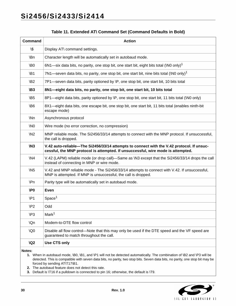
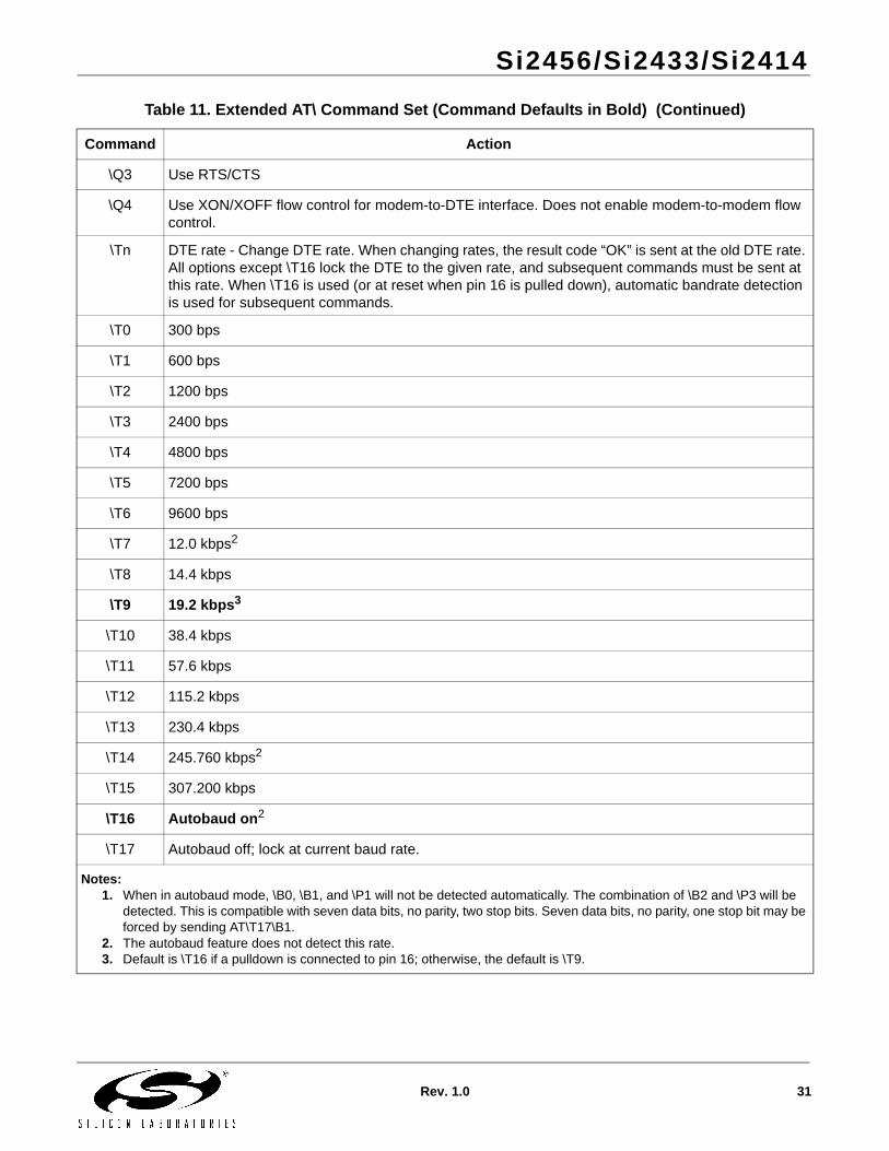
Table 11. Extended AT\ Command Set (Command Defaults in Bold)
Command Action
\$ Display AT\ command settings.
\Bn Character length will be automatically set in autobaud mode.
\B0 6N1—six data bits, no parity, one stop bit, one start bit, eight bits total (\N0 only)1
\B1 7N1—seven data bits, no parity, one stop bit, one start bit, nine bits total (\N0 only)1
\B2 7P1—seven data bits, parity optioned by \P, one stop bit, one start bit, 10 bits total
\B3 8N1—eight data bits, no parity, one stop bit, one start bit, 10 bits total
\B5 8P1—eight data bits, parity optioned by \P, one stop bit, one start bit, 11 bits total (\N0 only)
\B6 8X1—eight data bits, one escape bit, one stop bit, one start bit, 11 bits total (enables ninth-bit escape mode)
\Nn Asynchronous protocol
\N0 Wire mode (no error correction, no compression)
\N2 MNP reliable mode. The Si2456/33/14 attempts to connect with the MNP protocol. If unsuccessful, the call is dropped.
\N3 V.42 auto-reliable—The Si2456/33/14 attempts to connect with the V.42 protocol. If unsuc-cessful, the MNP protocol is attempted. If unsuccessful, wire mode is attempted.
\N4 V.42 (LAPM) reliable mode (or drop call)—Same as \N3 except that the Si2456/33/14 drops the call instead of connecting in MNP or wire mode.
\N5 V.42 and MNP reliable mode - The Si2456/33/14 attempts to connect with V.42. If unsuccessful, MNP is attempted. If MNP is unsuccessful, the call is dropped.
\Pn Parity type will be automatically set in autobaud mode.
\P0 Even
\P1 Space1
\P2 Odd
\P3 Mark1
\Qn Modem-to-DTE flow control
\Q0 Disable all flow control—Note that this may only be used if the DTE speed and the VF speed are guaranteed to match throughout the call.
\Q2 Use CTS only
Notes:1. When in autobaud mode, \B0, \B1, and \P1 will not be detected automatically. The combination of \B2 and \P3 will be
detected. This is compatible with seven data bits, no parity, two stop bits. Seven data bits, no parity, one stop bit may be forced by sending AT\T17\B1.
2. The autobaud feature does not detect this rate.3. Default is \T16 if a pulldown is connected to pin 16; otherwise, the default is \T9.
Si2456/Si2433/Si2414
Rev. 1.0 31
\Q3 Use RTS/CTS
\Q4 Use XON/XOFF flow control for modem-to-DTE interface. Does not enable modem-to-modem flow control.
\Tn DTE rate - Change DTE rate. When changing rates, the result code “OK” is sent at the old DTE rate. All options except \T16 lock the DTE to the given rate, and subsequent commands must be sent at this rate. When \T16 is used (or at reset when pin 16 is pulled down), automatic bandrate detection is used for subsequent commands.
\T0 300 bps
\T1 600 bps
\T2 1200 bps
\T3 2400 bps
\T4 4800 bps
\T5 7200 bps
\T6 9600 bps
\T7 12.0 kbps2
\T8 14.4 kbps
\T9 19.2 kbps3
\T10 38.4 kbps
\T11 57.6 kbps
\T12 115.2 kbps
\T13 230.4 kbps
\T14 245.760 kbps2
\T15 307.200 kbps
\T16 Autobaud on2
\T17 Autobaud off; lock at current baud rate.
Table 11. Extended AT\ Command Set (Command Defaults in Bold) (Continued)
Command Action
Notes:1. When in autobaud mode, \B0, \B1, and \P1 will not be detected automatically. The combination of \B2 and \P3 will be
detected. This is compatible with seven data bits, no parity, two stop bits. Seven data bits, no parity, one stop bit may be forced by sending AT\T17\B1.
2. The autobaud feature does not detect this rate.3. Default is \T16 if a pulldown is connected to pin 16; otherwise, the default is \T9.
Si2456/Si2433/Si2414
32 Rev. 1.0
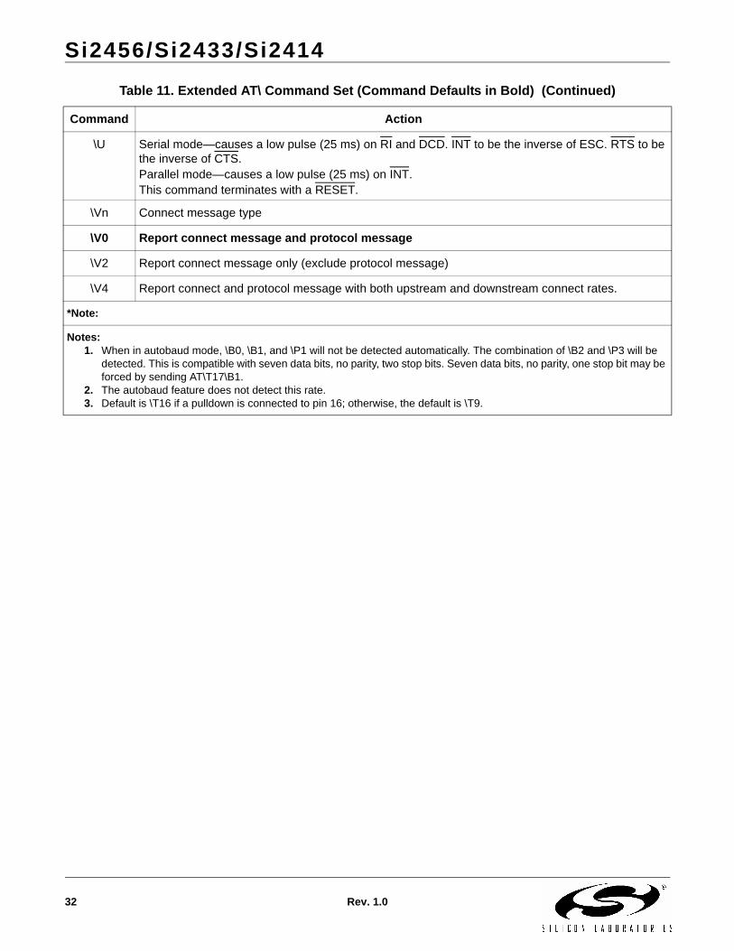
\U Serial mode—causes a low pulse (25 ms) on RI and DCD. INT to be the inverse of ESC. RTS to be the inverse of CTS.Parallel mode—causes a low pulse (25 ms) on INT. This command terminates with a RESET.
\Vn Connect message type
\V0 Report connect message and protocol message
\V2 Report connect message only (exclude protocol message)
\V4 Report connect and protocol message with both upstream and downstream connect rates.
*Note:
Table 11. Extended AT\ Command Set (Command Defaults in Bold) (Continued)
Command Action
Notes:1. When in autobaud mode, \B0, \B1, and \P1 will not be detected automatically. The combination of \B2 and \P3 will be
detected. This is compatible with seven data bits, no parity, two stop bits. Seven data bits, no parity, one stop bit may be forced by sending AT\T17\B1.
2. The autobaud feature does not detect this rate.3. Default is \T16 if a pulldown is connected to pin 16; otherwise, the default is \T9.
Si2456/Si2433/Si2414
Rev. 1.0 33
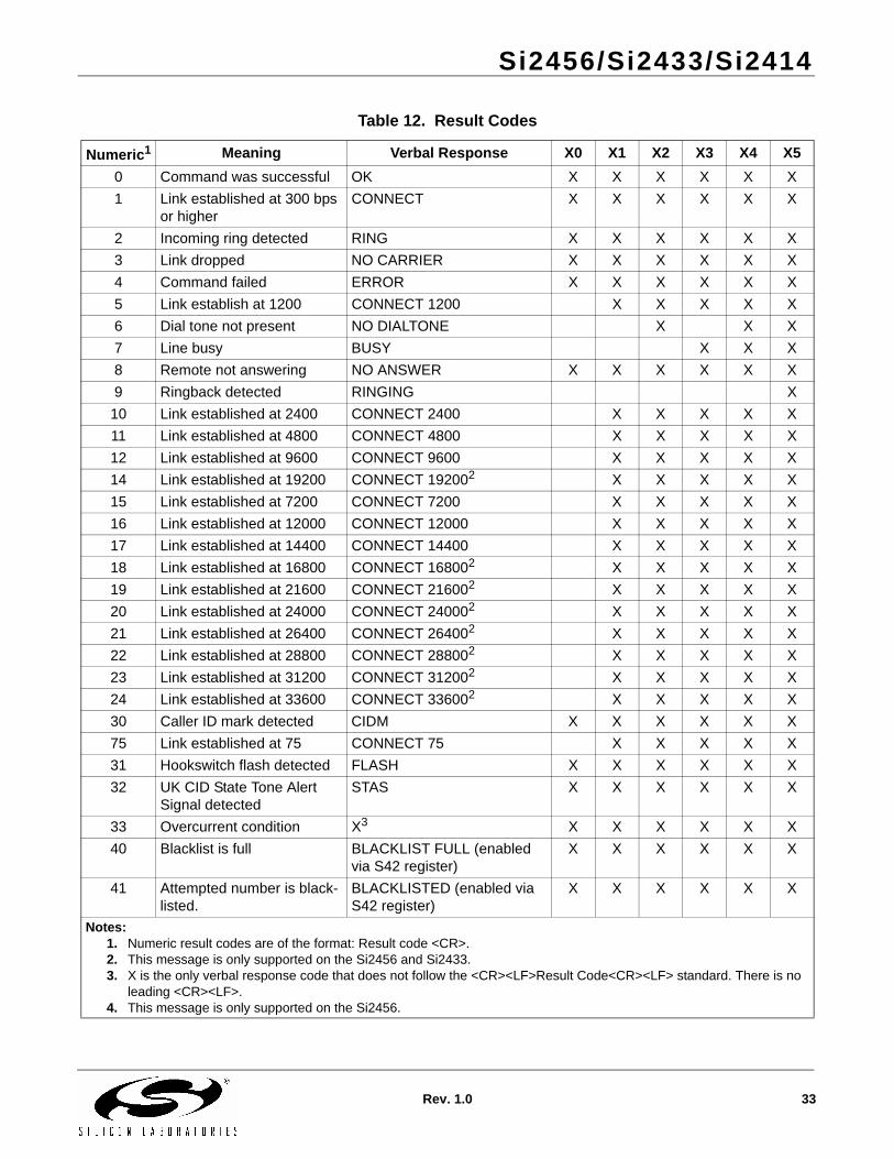
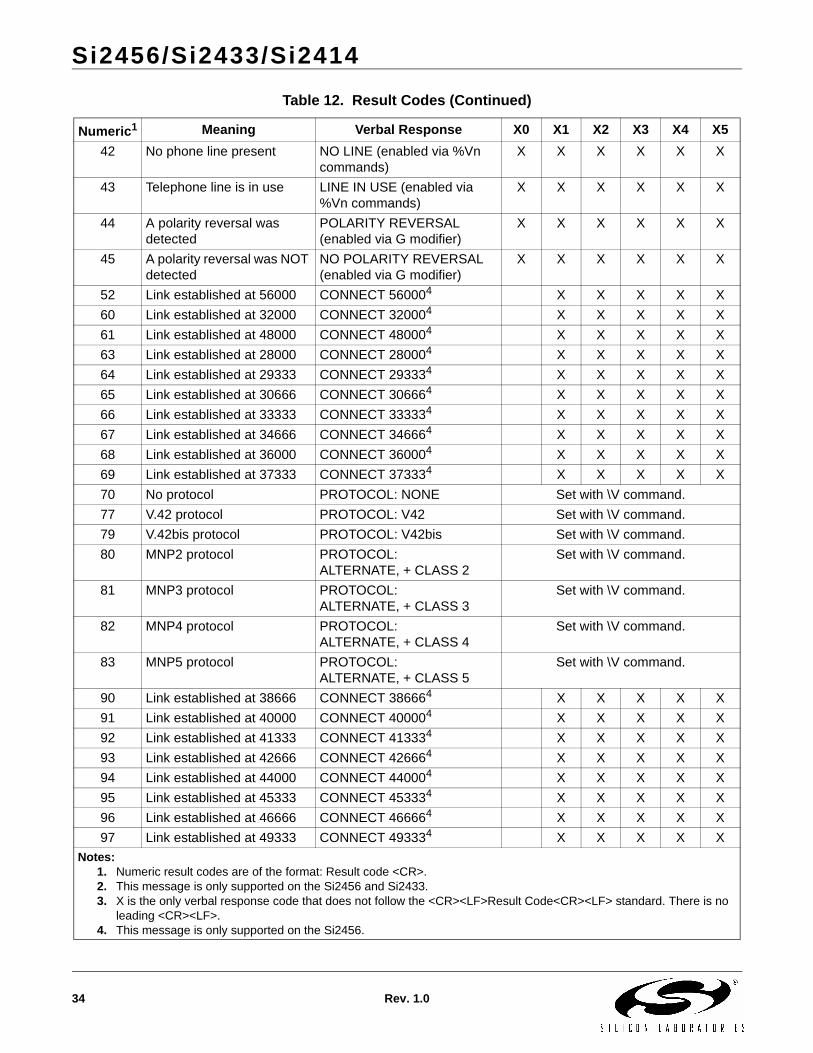
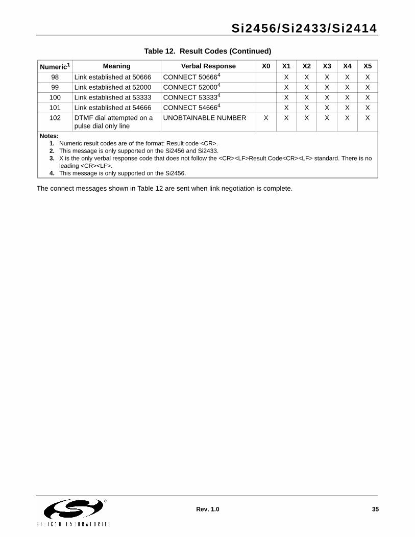
Table 12. Result Codes
Numeric1 Meaning Verbal Response X0 X1 X2 X3 X4 X50 Command was successful OK X X X X X X1 Link established at 300 bps
or higherCONNECT X X X X X X
2 Incoming ring detected RING X X X X X X3 Link dropped NO CARRIER X X X X X X4 Command failed ERROR X X X X X X5 Link establish at 1200 CONNECT 1200 X X X X X6 Dial tone not present NO DIALTONE X X X7 Line busy BUSY X X X8 Remote not answering NO ANSWER X X X X X X9 Ringback detected RINGING X10 Link established at 2400 CONNECT 2400 X X X X X11 Link established at 4800 CONNECT 4800 X X X X X12 Link established at 9600 CONNECT 9600 X X X X X14 Link established at 19200 CONNECT 192002 X X X X X15 Link established at 7200 CONNECT 7200 X X X X X16 Link established at 12000 CONNECT 12000 X X X X X17 Link established at 14400 CONNECT 14400 X X X X X18 Link established at 16800 CONNECT 168002 X X X X X19 Link established at 21600 CONNECT 216002 X X X X X20 Link established at 24000 CONNECT 240002 X X X X X21 Link established at 26400 CONNECT 264002 X X X X X22 Link established at 28800 CONNECT 288002 X X X X X23 Link established at 31200 CONNECT 312002 X X X X X24 Link established at 33600 CONNECT 336002 X X X X X30 Caller ID mark detected CIDM X X X X X X75 Link established at 75 CONNECT 75 X X X X X31 Hookswitch flash detected FLASH X X X X X X32 UK CID State Tone Alert
Signal detectedSTAS X X X X X X
33 Overcurrent condition X3 X X X X X X40 Blacklist is full BLACKLIST FULL (enabled
via S42 register)X X X X X X
41 Attempted number is black-listed.
BLACKLISTED (enabled via S42 register)
X X X X X X
Notes:1. Numeric result codes are of the format: Result code <CR>.2. This message is only supported on the Si2456 and Si2433.3. X is the only verbal response code that does not follow the <CR><LF>Result Code<CR><LF> standard. There is no
leading <CR><LF>. 4. This message is only supported on the Si2456.
Si2456/Si2433/Si2414
34 Rev. 1.0
42 No phone line present NO LINE (enabled via %Vn commands)
X X X X X X
43 Telephone line is in use LINE IN USE (enabled via %Vn commands)
X X X X X X
44 A polarity reversal was detected
POLARITY REVERSAL (enabled via G modifier)
X X X X X X
45 A polarity reversal was NOT detected
NO POLARITY REVERSAL (enabled via G modifier)
X X X X X X
52 Link established at 56000 CONNECT 560004 X X X X X60 Link established at 32000 CONNECT 320004 X X X X X61 Link established at 48000 CONNECT 480004 X X X X X63 Link established at 28000 CONNECT 280004 X X X X X64 Link established at 29333 CONNECT 293334 X X X X X65 Link established at 30666 CONNECT 306664 X X X X X66 Link established at 33333 CONNECT 333334 X X X X X67 Link established at 34666 CONNECT 346664 X X X X X68 Link established at 36000 CONNECT 360004 X X X X X69 Link established at 37333 CONNECT 373334 X X X X X70 No protocol PROTOCOL: NONE Set with \V command.77 V.42 protocol PROTOCOL: V42 Set with \V command.79 V.42bis protocol PROTOCOL: V42bis Set with \V command.80 MNP2 protocol PROTOCOL:
ALTERNATE, + CLASS 2Set with \V command.
81 MNP3 protocol PROTOCOL: ALTERNATE, + CLASS 3
Set with \V command.
82 MNP4 protocol PROTOCOL: ALTERNATE, + CLASS 4
Set with \V command.
83 MNP5 protocol PROTOCOL: ALTERNATE, + CLASS 5
Set with \V command.
90 Link established at 38666 CONNECT 386664 X X X X X91 Link established at 40000 CONNECT 400004 X X X X X92 Link established at 41333 CONNECT 413334 X X X X X93 Link established at 42666 CONNECT 426664 X X X X X94 Link established at 44000 CONNECT 440004 X X X X X95 Link established at 45333 CONNECT 453334 X X X X X96 Link established at 46666 CONNECT 466664 X X X X X97 Link established at 49333 CONNECT 493334 X X X X X
Table 12. Result Codes (Continued)
Numeric1 Meaning Verbal Response X0 X1 X2 X3 X4 X5
Notes:1. Numeric result codes are of the format: Result code <CR>.2. This message is only supported on the Si2456 and Si2433.3. X is the only verbal response code that does not follow the <CR><LF>Result Code<CR><LF> standard. There is no
leading <CR><LF>. 4. This message is only supported on the Si2456.
Si2456/Si2433/Si2414
Rev. 1.0 35
The connect messages shown in Table 12 are sent when link negotiation is complete.
98 Link established at 50666 CONNECT 506664 X X X X X99 Link established at 52000 CONNECT 520004 X X X X X100 Link established at 53333 CONNECT 533334 X X X X X101 Link established at 54666 CONNECT 546664 X X X X X102 DTMF dial attempted on a
pulse dial only lineUNOBTAINABLE NUMBER X X X X X X
Table 12. Result Codes (Continued)
Numeric1 Meaning Verbal Response X0 X1 X2 X3 X4 X5
Notes:1. Numeric result codes are of the format: Result code <CR>.2. This message is only supported on the Si2456 and Si2433.3. X is the only verbal response code that does not follow the <CR><LF>Result Code<CR><LF> standard. There is no
leading <CR><LF>. 4. This message is only supported on the Si2456.
Si2456/Si2433/Si2414
36 Rev. 1.0
S-RegistersThe S command allows reading (Sn?) or writing (Sn=x) the S-registers. The S-registers store values for functionsthat typically are rarely changed, such as timers or counters, and the ASCII values of control characters, such ascarriage return. Table 13 summarizes the S-register set.
Table 13. S-Register Descriptions
Definition
S-Register(Decimal) Function Default
(Decimal) Range Units
0 Automatic answer—Number of rings the Si2456/33/14 must detect before answering a call. 0 disables auto answer.
0 0–255 Rings
1 Ring counter. 0 0–255 Rings
2 ESC code character. 43 (+) 0–255 ASCII
3 Carriage return character. 13 (CR) 0–255 ASCII
4 Linefeed character. 10 (LF) 0–255 ASCII
5 Backspace character. 08 (BS) 0–255 ASCII
6 Dial tone wait timer—Number of seconds the Si2456/33/14 waits before blind dialing. Only applicable if blind dialing is enabled (X0, X1, X3).
02 0–255 seconds
7 Carrier wait timer—Number of seconds the Si2456/33/14 waits for carrier before timing out. This register also sets the number of seconds the modem waits for ring-back when originating a call before hanging up. This register also sets the number of seconds the answer tone will continue while using the AT*Y2A command.
80 0–255 seconds
8 Dial pause timer for , and < dial command modifiers. 02 0–255 seconds
9 Carrier presence timer—Time after a loss of carrier that a carrier must be detected before reactivating DCD. S9 is referred to as “carrier loss debounce time.”
06 1–255 0.1 seconds
10 Carrier loss timer—Time the carrier must be lost before the Si2456/33/14 disconnects. Setting 255 dis-ables disconnect entirely. If S10 is less than S9, even a momentary loss of carrier causes a disconnect.
14 1–255 0.1 seconds
12 Escape code guard timer—Minimum guard time required before and after “+++” for the Si2456/33/14 to recognize a valid escape sequence.
50 1–255 0.02 seconds
14 Wait for dial tone delay value (in relation to the W dial modifier). Starts when “W” is executed in the dial string.
12 0–255 seconds
Si2456/Si2433/Si2414
Rev. 1.0 37
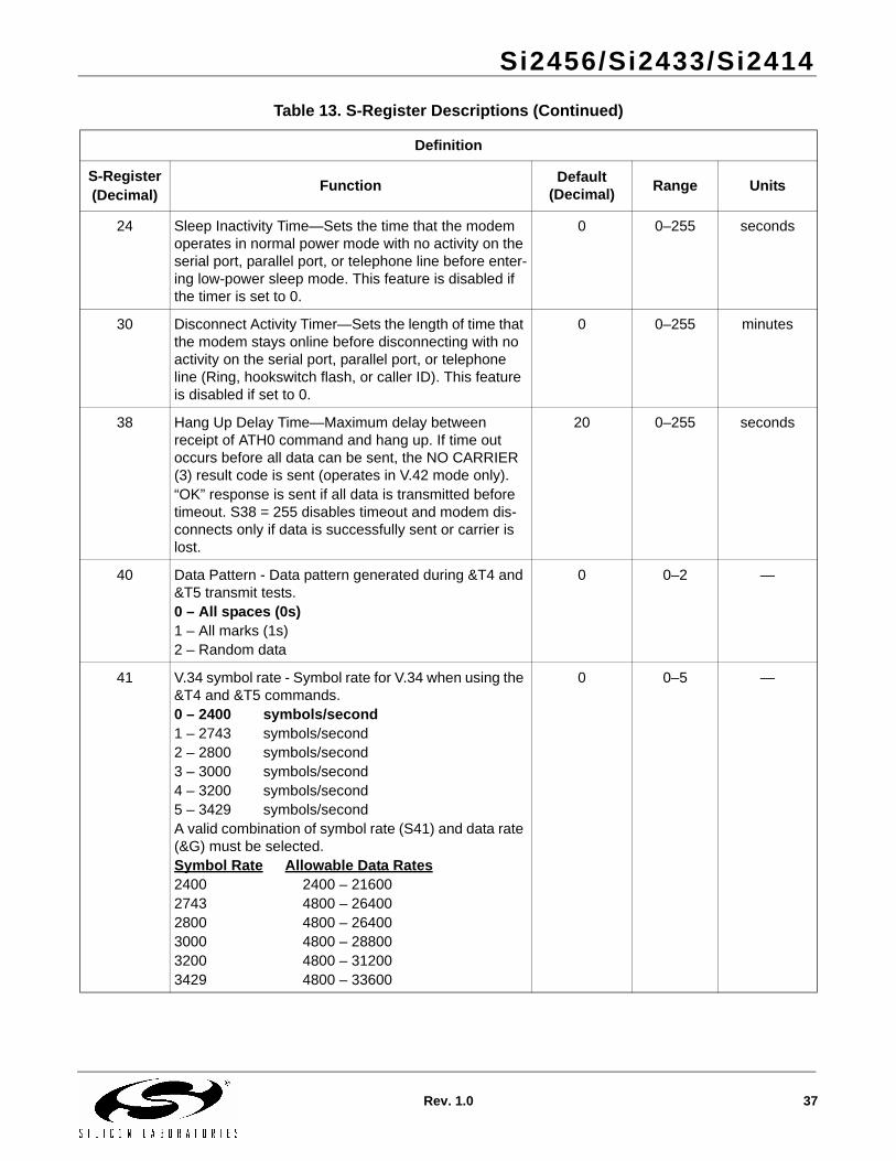
24 Sleep Inactivity Time—Sets the time that the modem operates in normal power mode with no activity on the serial port, parallel port, or telephone line before enter-ing low-power sleep mode. This feature is disabled if the timer is set to 0.
0 0–255 seconds
30 Disconnect Activity Timer—Sets the length of time that the modem stays online before disconnecting with no activity on the serial port, parallel port, or telephone line (Ring, hookswitch flash, or caller ID). This feature is disabled if set to 0.
0 0–255 minutes
38 Hang Up Delay Time—Maximum delay between receipt of ATH0 command and hang up. If time out occurs before all data can be sent, the NO CARRIER (3) result code is sent (operates in V.42 mode only).“OK” response is sent if all data is transmitted before timeout. S38 = 255 disables timeout and modem dis-connects only if data is successfully sent or carrier is lost.
20 0–255 seconds
40 Data Pattern - Data pattern generated during &T4 and &T5 transmit tests.0 – All spaces (0s)1 – All marks (1s)2 – Random data
0 0–2 —
41 V.34 symbol rate - Symbol rate for V.34 when using the &T4 and &T5 commands.0 – 2400 symbols/second1 – 2743 symbols/second2 – 2800 symbols/second3 – 3000 symbols/second4 – 3200 symbols/second5 – 3429 symbols/secondA valid combination of symbol rate (S41) and data rate (&G) must be selected.Symbol Rate Allowable Data Rates2400 2400 – 216002743 4800 – 264002800 4800 – 264003000 4800 – 288003200 4800 – 312003429 4800 – 33600
0 0–5 —
Table 13. S-Register Descriptions (Continued)
Definition
S-Register(Decimal) Function Default
(Decimal) Range Units
Si2456/Si2433/Si2414
38 Rev. 1.0
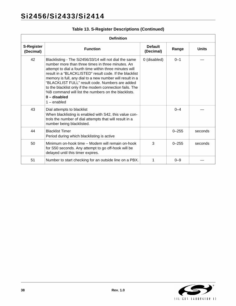
42 Blacklisting - The Si2456/33/14 will not dial the same number more than three times in three minutes. An attempt to dial a fourth time within three minutes will result in a “BLACKLISTED” result code. If the blacklist memory is full, any dial to a new number will result in a “BLACKLIST FULL” result code. Numbers are added to the blacklist only if the modem connection fails. The %B command will list the numbers on the blacklists.0 – disabled1 – enabled
0 (disabled) 0–1 —
43 Dial attempts to blacklistWhen blacklisting is enabled with S42, this value con-trols the number of dial attempts that will result in a number being blacklisted.
0–4 —
44 Blacklist TimerPeriod during which blacklisting is active
0–255 seconds
50 Minimum on-hook time – Modem will remain on-hook for S50 seconds. Any attempt to go off-hook will be delayed until this timer expires.
3 0–255 seconds
51 Number to start checking for an outside line on a PBX. 1 0–9 —
Table 13. S-Register Descriptions (Continued)
Definition
S-Register(Decimal) Function Default
(Decimal) Range Units
Si2456/Si2433/Si2414
Rev. 1.0 39
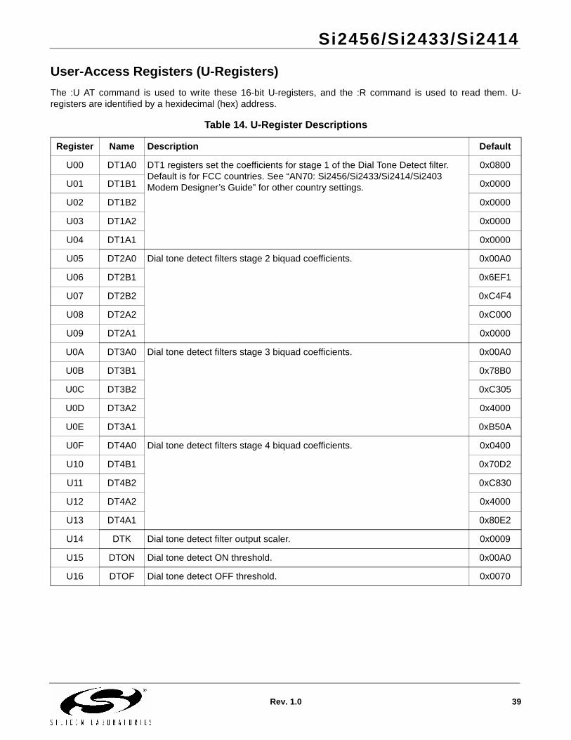
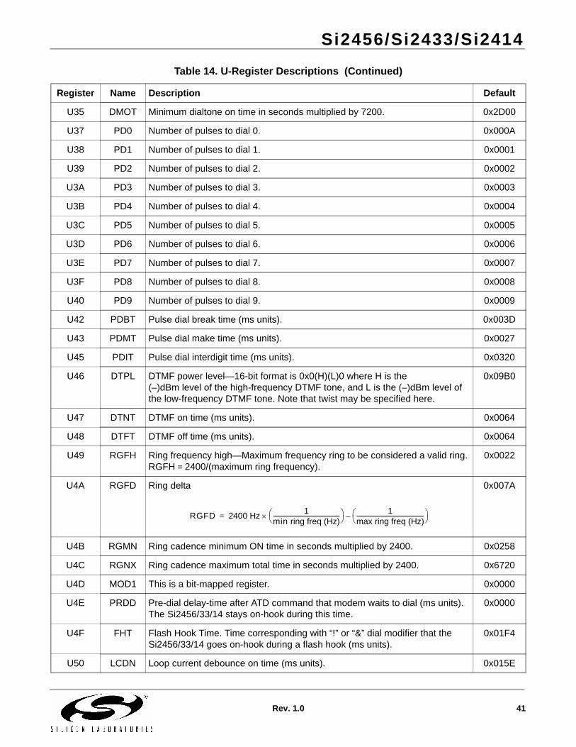
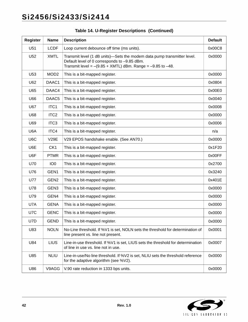
User-Access Registers (U-Registers)The :U AT command is used to write these 16-bit U-registers, and the :R command is used to read them. U-registers are identified by a hexidecimal (hex) address.
Table 14. U-Register Descriptions
Register Name Description Default
U00 DT1A0 DT1 registers set the coefficients for stage 1 of the Dial Tone Detect filter. Default is for FCC countries. See “AN70: Si2456/Si2433/Si2414/Si2403 Modem Designer’s Guide” for other country settings.
0x0800
U01 DT1B1 0x0000
U02 DT1B2 0x0000
U03 DT1A2 0x0000
U04 DT1A1 0x0000
U05 DT2A0 Dial tone detect filters stage 2 biquad coefficients. 0x00A0
U06 DT2B1 0x6EF1
U07 DT2B2 0xC4F4
U08 DT2A2 0xC000
U09 DT2A1 0x0000
U0A DT3A0 Dial tone detect filters stage 3 biquad coefficients. 0x00A0
U0B DT3B1 0x78B0
U0C DT3B2 0xC305
U0D DT3A2 0x4000
U0E DT3A1 0xB50A
U0F DT4A0 Dial tone detect filters stage 4 biquad coefficients. 0x0400
U10 DT4B1 0x70D2
U11 DT4B2 0xC830
U12 DT4A2 0x4000
U13 DT4A1 0x80E2
U14 DTK Dial tone detect filter output scaler. 0x0009
U15 DTON Dial tone detect ON threshold. 0x00A0
U16 DTOF Dial tone detect OFF threshold. 0x0070
Si2456/Si2433/Si2414
40 Rev. 1.0
U17 BT1A0 BT1 registers set the coefficients for stage 1 of the Busy Tone Detect filter. Default is for FCC countries. See AN70 for other country settings.
0x0800
U18 BT1B1 0x0000
U19 BT1B2 0x0000
U1A BT1A2 0x0000
U1B BT1A1 0x0000
U1C BT2A0 Busy tone detect filter stage 2 biquad coefficients. 0x00A0
U1D BT2B1 0x6EF1
U1E BT2B2 0xC4F4
U1F BT2A2 0xC000
U20 BT2A1 0x0000
U21 BT3A0 Busy tone detect filter stage 3 biquad coefficients. 0x00A0
U22 BT3B1 0x78B0
U23 BT3B2 0xC305
U24 BT3A2 0x4000
U25 BT3A1 0xB50A
U26 BT4A0 Busy tone detect filter stage 4 biquad coefficients. 0x0400
U27 BT4B1 0x70D2
U28 BT4B2 0xC830
U29 BT4A2 0x4000
U2A BT4A1 0x80E2
U2B BTK Busy tone detect filter output scaler. 0x0009
U2C BTON Busy tone detect ON threshold. 0x00A0
U2D BTOF Busy tone detect OFF threshold. 0x0070
U2E BMTT Busy cadence minimum total time in seconds multiplied by 7200. 0x0870
U2F BDLT Busy cadence delta in seconds multiplied by 7200. 0x25F8
U30 BMOT Busy cadence minimum on time in seconds multiplied by 7200. 0x0438
U31 RMTT Ringback cadence minimum total time in seconds multiplied by 7200. 0x4650
U32 RDLT Ringback cadence delta in seconds multiplied by 7200. 0xEF10
U33 RMOT Ringback cadence minimum on time in seconds multiplied by 7200. 0x1200
U34 DTWD Window to look for dialtone in seconds multiplied by 1000. 0x1B58
Table 14. U-Register Descriptions (Continued)
Register Name Description Default
Si2456/Si2433/Si2414
Rev. 1.0 41
U35 DMOT Minimum dialtone on time in seconds multiplied by 7200. 0x2D00
U37 PD0 Number of pulses to dial 0. 0x000A
U38 PD1 Number of pulses to dial 1. 0x0001
U39 PD2 Number of pulses to dial 2. 0x0002
U3A PD3 Number of pulses to dial 3. 0x0003
U3B PD4 Number of pulses to dial 4. 0x0004
U3C PD5 Number of pulses to dial 5. 0x0005
U3D PD6 Number of pulses to dial 6. 0x0006
U3E PD7 Number of pulses to dial 7. 0x0007
U3F PD8 Number of pulses to dial 8. 0x0008
U40 PD9 Number of pulses to dial 9. 0x0009
U42 PDBT Pulse dial break time (ms units). 0x003D
U43 PDMT Pulse dial make time (ms units). 0x0027
U45 PDIT Pulse dial interdigit time (ms units). 0x0320
U46 DTPL DTMF power level—16-bit format is 0x0(H)(L)0 where H is the (–)dBm level of the high-frequency DTMF tone, and L is the (–)dBm level of the low-frequency DTMF tone. Note that twist may be specified here.
0x09B0
U47 DTNT DTMF on time (ms units). 0x0064
U48 DTFT DTMF off time (ms units). 0x0064
U49 RGFH Ring frequency high—Maximum frequency ring to be considered a valid ring. RGFH = 2400/(maximum ring frequency).
0x0022
U4A RGFD Ring delta 0x007A
U4B RGMN Ring cadence minimum ON time in seconds multiplied by 2400. 0x0258
U4C RGNX Ring cadence maximum total time in seconds multiplied by 2400. 0x6720
U4D MOD1 This is a bit-mapped register. 0x0000
U4E PRDD Pre-dial delay-time after ATD command that modem waits to dial (ms units). The Si2456/33/14 stays on-hook during this time.
0x0000
U4F FHT Flash Hook Time. Time corresponding with “!” or “&” dial modifier that the Si2456/33/14 goes on-hook during a flash hook (ms units).
0x01F4
U50 LCDN Loop current debounce on time (ms units). 0x015E
Table 14. U-Register Descriptions (Continued)
Register Name Description Default
RGFD 2400 Hz 1min ring freq (Hz)-----------------------------------------------
× 1max ring freq (Hz)------------------------------------------------
–=
Si2456/Si2433/Si2414
42 Rev. 1.0
U51 LCDF Loop current debounce off time (ms units). 0x00C8
U52 XMTL Transmit level (1 dB units)—Sets the modem data pump transmitter level. Default level of 0 corresponds to –9.85 dBm. Transmit level = –(9.85 + XMTL) dBm. Range = –9.85 to –48.
0x0000
U53 MOD2 This is a bit-mapped register. 0x0000
U62 DAAC1 This is a bit-mapped register. 0x0804
U65 DAAC4 This is a bit-mapped register. 0x00E0
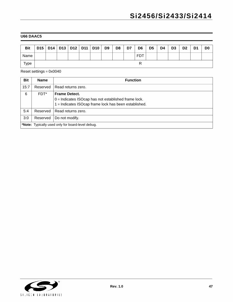
U66 DAAC5 This is a bit-mapped register. 0x0040
U67 ITC1 This is a bit-mapped register. 0x0008
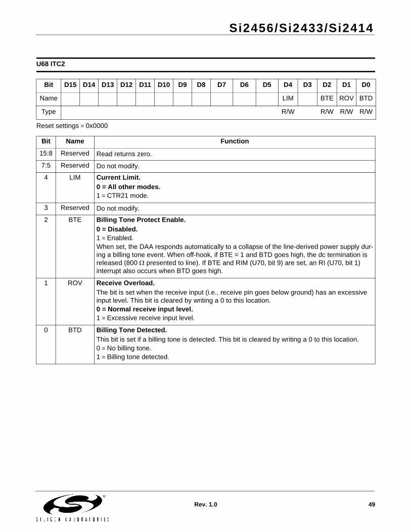
U68 ITC2 This is a bit-mapped register. 0x0000
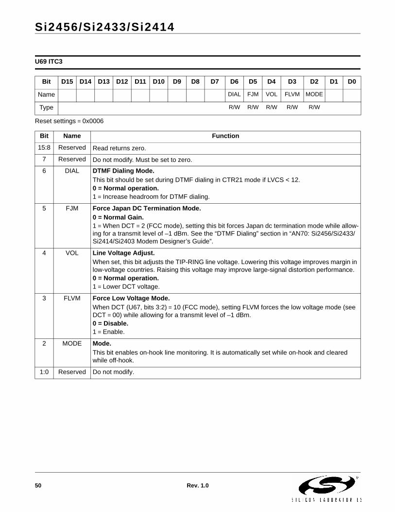
U69 ITC3 This is a bit-mapped register. 0x0006
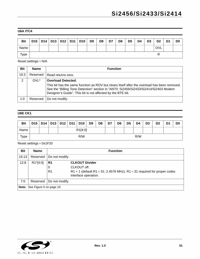
U6A ITC4 This is a bit-mapped register. n/a
U6C V29E V29 EPOS handshake enable. (See AN70.) 0x0000
U6E CK1 This is a bit-mapped register. 0x1F20
U6F PTMR This is a bit-mapped register. 0x00FF
U70 IO0 This is a bit-mapped register. 0x2700
U76 GEN1 This is a bit-mapped register. 0x3240
U77 GEN2 This is a bit-mapped register. 0x401E
U78 GEN3 This is a bit-mapped register. 0x0000
U79 GEN4 This is a bit-mapped register. 0x0000
U7A GENA This is a bit-mapped register. 0x0000
U7C GENC This is a bit-mapped register. 0x0000
U7D GEND This is a bit-mapped register. 0x0000
U83 NOLN No-Line threshold. If %V1 is set, NOLN sets the threshold for determination of line present vs. line not present.
0x0001
U84 LIUS Line-in-use threshold. If %V1 is set, LIUS sets the threshold for determination of line in use vs. line not in use.
0x0007
U85 NLIU Line-in-use/No line threshold. If %V2 is set, NLIU sets the threshold reference for the adaptive algorithm (see %V2).
0x0000
U86 V9AGG V.90 rate reduction in 1333 bps units. 0x0000
Table 14. U-Register Descriptions (Continued)
Register Name Description Default
Si2456/Si2433/Si2414
Rev. 1.0 43
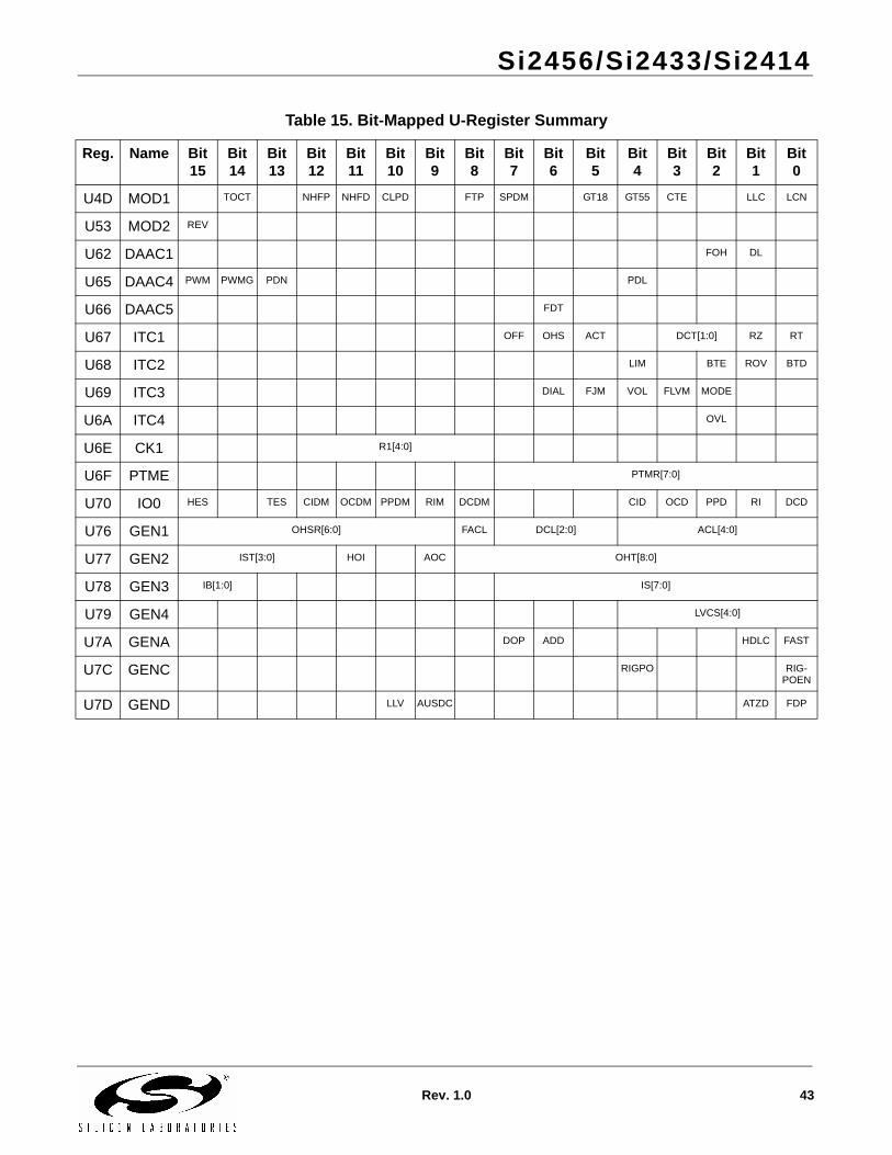
Table 15. Bit-Mapped U-Register Summary
Reg. Name Bit 15
Bit 14
Bit 13
Bit 12
Bit 11
Bit 10
Bit 9
Bit 8
Bit 7
Bit 6
Bit 5
Bit 4
Bit 3
Bit 2
Bit 1
Bit 0
U4D MOD1 TOCT NHFP NHFD CLPD FTP SPDM GT18 GT55 CTE LLC LCN
U53 MOD2 REV
U62 DAAC1 FOH DL
U65 DAAC4 PWM PWMG PDN PDL
U66 DAAC5 FDT
U67 ITC1 OFF OHS ACT DCT[1:0] RZ RT
U68 ITC2 LIM BTE ROV BTD
U69 ITC3 DIAL FJM VOL FLVM MODE
U6A ITC4 OVL
U6E CK1 R1[4:0]
U6F PTME PTMR[7:0]
U70 IO0 HES TES CIDM OCDM PPDM RIM DCDM CID OCD PPD RI DCD
U76 GEN1 OHSR[6:0] FACL DCL[2:0] ACL[4:0]
U77 GEN2 IST[3:0] HOI AOC OHT[8:0]
U78 GEN3 IB[1:0] IS[7:0]
U79 GEN4 LVCS[4:0]
U7A GENA DOP ADD HDLC FAST
U7C GENC RIGPO RIG-POEN
U7D GEND LLV AUSDC ATZD FDP
Si2456/Si2433/Si2414
44 Rev. 1.0
Bit-Mapped U-Register Detail (defaults in bold)
Reset settings = 0x0000
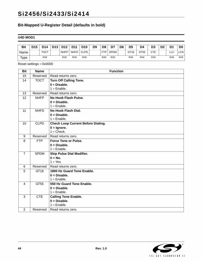
U4D MOD1
Bit D15 D14 D13 D12 D11 D10 D9 D8 D7 D6 D5 D4 D3 D2 D1 D0Name TOCT NHFP NHFD CLPD FTP SPDM GT18 GT55 CTE LLC LCN
Type R/W R/W R/W R/W R/W R/W R/W R/W R/W R/W R/W
Bit Name Function15 Reserved Read returns zero.14 TOCT Turn Off Calling Tone.
0 = Disable.1 = Enable.
13 Reserved Read returns zero.12 NHFP No Hook Flash Pulse.
0 = Disable.1 = Enable.
11 NHFD No Hook Flash Dial.0 = Disable.1 = Enable.
10 CLPD Check Loop Current Before Dialing.0 = Ignore.1 = Check.
9 Reserved Read returns zero.8 FTP Force Tone or Pulse.
0 = Disable.1 = Enable.
7 SPDM Skip Pulse Dial Modifier.0 = No.1 = Yes.
6 Reserved Read returns zero.5 GT18 1800 Hz Guard Tone Enable.
0 = Disable.1 = Enable.
4 GT55 550 Hz Guard Tone Enable.0 = Disable.1 = Enable.
3 CTE Calling Tone Enable.0 = Disable.1 = Enable.
2 Reserved Read returns zero.
Si2456/Si2433/Si2414
Rev. 1.0 45
Reset settings = 0x0000
Reset settings = 0x0804
1 LLC Low Loop Current Detect (required for CTR21).0 = Disabled.1 = Enabled.
0 LCN Loop Current Needed.0 = No.1 = Yes.
U53 MOD2
Bit D15 D14 D13 D12 D11 D10 D9 D8 D7 D6 D5 D4 D3 D2 D1 D0
Name REV
Type R/W
Bit Name Function15 REV V.23 Reversing.
0 = Disable.1 = Enable.
14:0 Reserved Read returns zero.
U62 DAAC1
Bit D15 D14 D13 D12 D11 D10 D9 D8 D7 D6 D5 D4 D3 D2 D1 D0
Name FOH DL
Type R/W R/W
Bit Name Function
15:12 Reserved Must be set to 0.
11 Reserved Must be set to 1.
10:3 Reserved Must be set to 0.
2 FOH Fast Off-Hook.0 = Automatic Calibration Time set to 426 ms1 = Automatic Calibration Time set to 106 ms
1 DL Isolation Digital Loopback (see the AT&T commands). 0 = Loopback occurs beyond the ISOcap interface, out to and including the analog hybrid circuit.1 = Enables digital loopback mode across isolation barrier only.
0 Reserved Must be set to 0.
Bit Name Function
Si2456/Si2433/Si2414
46 Rev. 1.0
Reset settings = 0x00E0
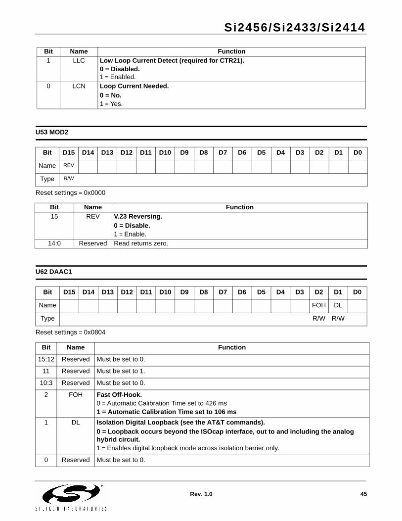
U65 DAAC4
Bit D15 D14 D13 D12 D11 D10 D9 D8 D7 D6 D5 D4 D3 D2 D1 D0
Name PWM PWMG PDN PDL
Type R/W R/W R/W R/W
Bit Name Function
15 PWM PWM Mode.0 = Normal. Classic PWM output waveform.1 = Scrambled mode. Low-distortion mode if used with output circuit shown in “AN70: Si2456/Si2433/Si2414/Si2403 Modem Designer’s Guide”.
14 PWMG PWM Gain.0 = No gain.1 = 6 dB gain applied to AOUT.
13 PDN Powerdown.Completely powerdown the Si2456/33/14 and Si3015. Once set to 1, the Si2456/33/14 must be reset to power on.0 = Normal.1 = Powerdown.
12:8 Reserved Read returns zero.
7:5 Reserved Must not change in a read-modify-write.
4 PDL* Powerdown Line-Side Chip.0 = Normal operation.1 = Places the Si3015 in powerdown mode.
3:0 Reserved Must not change in a read-modify-write.*Note: Typically used only for board-level debug.
Si2456/Si2433/Si2414
Rev. 1.0 47
Reset settings = 0x0040
U66 DAAC5
Bit D15 D14 D13 D12 D11 D10 D9 D8 D7 D6 D5 D4 D3 D2 D1 D0
Name FDT
Type R
Bit Name Function
15:7 Reserved Read returns zero.
6 FDT* Frame Detect. 0 = Indicates ISOcap has not established frame lock.1 = Indicates ISOcap frame lock has been established.
5:4 Reserved Read returns zero.
3:0 Reserved Do not modify.
*Note: Typically used only for board-level debug.
Si2456/Si2433/Si2414
48 Rev. 1.0
Reset settings = 0x0008
U67 ITC1
Bit D15 D14 D13 D12 D11 D10 D9 D8 D7 D6 D5 D4 D3 D2 D1 D0
Name OFF OHS ACT DCT[1:0] RZ RT
Type R/W R/W R/W R/W R/W R/W
Bit Name Function
15:8 Reserved Read returns zero.
7 OFF DC Termination Off.0 = Normal operation. The OFF bit must always be set to 0 when on-hook.1 = DC termination disabled and the device presents an 800 Ω dc impedance to the line, which is used to enhance operation with an off-hook parallel phone.
6 OHS On-Hook Speed.0 = The Si2456/33/14 will execute a fast on-hook.1 = The Si2456/33/14 will execute a slow controlled on-hook.
5 ACT AC Termination Select.0 = Selects the real impedance.1 = Selects the complex impedance.
4 Reserved Read returns zero.
3:2 DCT[1:0] DC Termination Select.00 = low voltage mode (Transmit level = –13.85 dBm).01 = Japan mode (Transmit level = –11.85 dBm).10 = FCC mode. Standard voltage mode (Transmit level = –9.85 dBm).11 = CTR21 mode. Current limiting mode (Transmit level = –9.85 dBm).
1 RZ Ringer Impedance.0 = Maximum (high) ringer impedance.1 = Synthesize ringer impedance. C15, R14, Z2, and Z3 must not be installed when setting this bit. See the “Ringer Impedance” section in “AN70: Si2456/Si2433/Si2414/Si2403 Modem Designer’s Guide”.
0 RT Ringer Threshold Select.Used to satisfy country requirements on ring detection. Signals below the lower level do not generate a ring detection; signals above the upper level are guaranteed to generate a ring detection.0 = 11 to 22 Vrms.1 = 17 to 33 Vrms.
Si2456/Si2433/Si2414
Rev. 1.0 49
Reset settings = 0x0000
U68 ITC2
Bit D15 D14 D13 D12 D11 D10 D9 D8 D7 D6 D5 D4 D3 D2 D1 D0
Name LIM BTE ROV BTD
Type R/W R/W R/W R/W
Bit Name Function
15:8 Reserved Read returns zero.
7:5 Reserved Do not modify.
4 LIM Current Limit.0 = All other modes.1 = CTR21 mode.
3 Reserved Do not modify.
2 BTE Billing Tone Protect Enable.0 = Disabled.1 = Enabled.When set, the DAA responds automatically to a collapse of the line-derived power supply dur-ing a billing tone event. When off-hook, if BTE = 1 and BTD goes high, the dc termination is released (800 Ω presented to line). If BTE and RIM (U70, bit 9) are set, an RI (U70, bit 1) interrupt also occurs when BTD goes high.
1 ROV Receive Overload.The bit is set when the receive input (i.e., receive pin goes below ground) has an excessive input level. This bit is cleared by writing a 0 to this location.0 = Normal receive input level.1 = Excessive receive input level.
0 BTD Billing Tone Detected.This bit is set if a billing tone is detected. This bit is cleared by writing a 0 to this location.0 = No billing tone.1 = Billing tone detected.
Si2456/Si2433/Si2414
50 Rev. 1.0
Reset settings = 0x0006
U69 ITC3
Bit D15 D14 D13 D12 D11 D10 D9 D8 D7 D6 D5 D4 D3 D2 D1 D0
Name DIAL FJM VOL FLVM MODE
Type R/W R/W R/W R/W R/W
Bit Name Function
15:8 Reserved Read returns zero.
7 Reserved Do not modify. Must be set to zero.
6 DIAL DTMF Dialing Mode.This bit should be set during DTMF dialing in CTR21 mode if LVCS < 12.0 = Normal operation.1 = Increase headroom for DTMF dialing.
5 FJM Force Japan DC Termination Mode.0 = Normal Gain.1 = When DCT = 2 (FCC mode), setting this bit forces Japan dc termination mode while allow-ing for a transmit level of –1 dBm. See the “DTMF Dialing” section in “AN70: Si2456/Si2433/Si2414/Si2403 Modem Designer’s Guide”.
4 VOL Line Voltage Adjust.When set, this bit adjusts the TIP-RING line voltage. Lowering this voltage improves margin in low-voltage countries. Raising this voltage may improve large-signal distortion performance.0 = Normal operation.1 = Lower DCT voltage.
3 FLVM Force Low Voltage Mode.When DCT (U67, bits 3:2) = 10 (FCC mode), setting FLVM forces the low voltage mode (see DCT = 00) while allowing for a transmit level of –1 dBm.0 = Disable.1 = Enable.
2 MODE Mode.This bit enables on-hook line monitoring. It is automatically set while on-hook and cleared while off-hook.
1:0 Reserved Do not modify.
Si2456/Si2433/Si2414
Rev. 1.0 51
Reset settings = N/A
Reset settings = 0x1F20
U6A ITC4
Bit D15 D14 D13 D12 D11 D10 D9 D8 D7 D6 D5 D4 D3 D2 D1 D0
Name OVL
Type R
Bit Name Function
15:3 Reserved Read returns zero.
2 OVL* Overload Detected.This bit has the same function as ROV but clears itself after the overload has been removed. See the “Billing Tone Detection” section in “AN70: Si2456/Si2433/Si2414/Si2403 Modem Designer’s Guide”. This bit is not affected by the BTE bit.
1:0 Reserved Do not modify.
U6E CK1
Bit D15 D14 D13 D12 D11 D10 D9 D8 D7 D6 D5 D4 D3 D2 D1 D0
Name R1[4:0]
Type R/W R/W
Bit Name Function
15:13 Reserved Do not modify.
12:8 R1*[4:0] R1 CLKOUT Divider0 CLKOUT off.R1 R1 + 1 (default R1 = 31; 2.4576 MHz). R1 = 31 required for proper codec
interface operation.
7:0 Reserved Do not modify.
Note: See Figure 5 on page 19.
Si2456/Si2433/Si2414
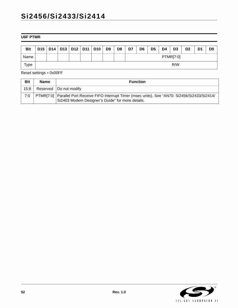
52 Rev. 1.0
Reset settings = 0x00FF
U6F PTMR
Bit D15 D14 D13 D12 D11 D10 D9 D8 D7 D6 D5 D4 D3 D2 D1 D0
Name PTMR[7:0]
Type R/W
Bit Name Function
15:8 Reserved Do not modify
7:0 PTMR[7:0] Parallel Port Receive FIFO Interrupt Timer (msec units). See “AN70: Si2456/Si2433/Si2414/Si2403 Modem Designer’s Guide” for more details.
Si2456/Si2433/Si2414
Rev. 1.0 53
Reset settings = 0x2700
U70 IO0
Bit D15 D14 D13 D12 D11 D10 D9 D8 D7 D6 D5 D4 D3 D2 D1 D0Name HES TES CIDM OCDM PPDM RIM DCDM CID OCD PPD RI DCD
Type R/W R/W R/W R/W R/W R/W R/W R/W R/W R/W R/W R/W
Bit Name Function15 HES Hardware Escape Pin.
0 = Disable.1 = Enable.
14 Reserved Read returns zero.13 TES Enable “+++” Escape.
0 = Disable.1 = Enable.
12 CIDM Caller ID Mask.0 = Change in CID will not affect INT.1 = A low-to-high transition in CID activates INT.
11 OCDM Overcurrent Detect Mask.0 = Change in OCD does not affect INT. (“X” result code is not generated in Command mode.)1 = A low-to-high transition in OCD will activate INT. (“X” result code is generated in Command mode.)
10 PPDM Parallel Phone Detect Mask.0 = Change in PPD does not affect INT.1 = A low-to-high transition in PPD will activate INT.
9 RIM Ring Indicator.0 = Change in RI does not affect INT.1 = A low-to-high transition in RI activates INT.
8 DCDM Data Carrier Detect Mask.0 = Change in DCD does not affect INT.1 = A high-to-low transition in DCD (U70, bit 0), which indicates loss of carrier, activates INT.
7 Reserved Must be set to zero.6:5 Reserved Read returns zero.4 CID Caller ID (sticky).
Caller ID preamble has been detected; data will soon follow. Clears on :I read.3 OCD Overcurrent Detect (sticky).
Overcurrent condition has occurred. Clears on :I read.2 PPD Parallel Phone Detect (sticky).
Parallel phone detected since last off-hook event. Clears on :I read.1 RI Ring Indicator.
Active high bit when the Si2456/33/14 is on-hook indicates ring event has occurred. Clears on :I read.
0 DCD Data Carrier Detect (status).Active high bit indicates carrier detected (equivalent to inverse of DCD pin).
Si2456/Si2433/Si2414
54 Rev. 1.0
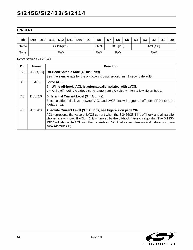
Reset settings = 0x3240
U76 GEN1
Bit D15 D14 D13 D12 D11 D10 D9 D8 D7 D6 D5 D4 D3 D2 D1 D0
Name OHSR[6:0] FACL DCL[2:0] ACL[4:0]
Type R/W R/W R/W R/W
Bit Name Function
15:9 OHSR[6:0] Off-Hook Sample Rate (40 ms units) Sets the sample rate for the off-hook intrusion algorithms (1 second default).
8 FACL Force ACL.0 = While off-hook, ACL is automatically updated with LVCS.1 = While off-hook, ACL does not change from the value written to it while on-hook.
7:5 DCL[2:0] Differential Current Level (3 mA units).Sets the differential level between ACL and LVCS that will trigger an off-hook PPD interrupt (default = 2).
4:0 ACL[4:0] Absolute Current Level (3 mA units, see Figure 7 on page 20).ACL represents the value of LVCS current when the Si2456/33/14 is off-hook and all parallel phones are on-hook. If ACL = 0, it is ignored by the off-hook intrusion algorithm.The Si2456/33/14 will also write ACL with the contents of LVCS before an intrusion and before going on-hook (default = 0).
Si2456/Si2433/Si2414
Rev. 1.0 55
Reset settings = 0x401E
U77 GEN2
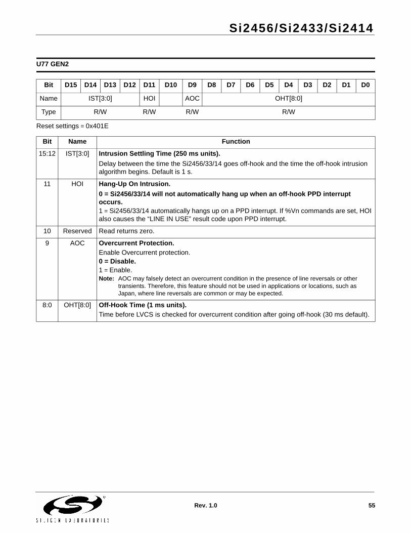
Bit D15 D14 D13 D12 D11 D10 D9 D8 D7 D6 D5 D4 D3 D2 D1 D0
Name IST[3:0] HOI AOC OHT[8:0]
Type R/W R/W R/W R/W
Bit Name Function
15:12 IST[3:0] Intrusion Settling Time (250 ms units).Delay between the time the Si2456/33/14 goes off-hook and the time the off-hook intrusion algorithm begins. Default is 1 s.
11 HOI Hang-Up On Intrusion.0 = Si2456/33/14 will not automatically hang up when an off-hook PPD interrupt occurs.1 = Si2456/33/14 automatically hangs up on a PPD interrupt. If %Vn commands are set, HOI also causes the “LINE IN USE” result code upon PPD interrupt.
10 Reserved Read returns zero.
9 AOC Overcurrent Protection.Enable Overcurrent protection.0 = Disable.1 = Enable.Note: AOC may falsely detect an overcurrent condition in the presence of line reversals or other
transients. Therefore, this feature should not be used in applications or locations, such as Japan, where line reversals are common or may be expected.
8:0 OHT[8:0] Off-Hook Time (1 ms units).Time before LVCS is checked for overcurrent condition after going off-hook (30 ms default).
Si2456/Si2433/Si2414
56 Rev. 1.0
Reset settings = 0x0000
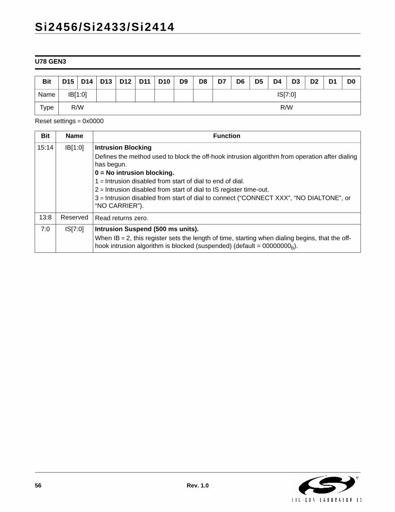
U78 GEN3
Bit D15 D14 D13 D12 D11 D10 D9 D8 D7 D6 D5 D4 D3 D2 D1 D0
Name IB[1:0] IS[7:0]
Type R/W R/W
Bit Name Function
15:14 IB[1:0] Intrusion BlockingDefines the method used to block the off-hook intrusion algorithm from operation after dialing has begun.0 = No intrusion blocking.1 = Intrusion disabled from start of dial to end of dial.2 = Intrusion disabled from start of dial to IS register time-out.3 = Intrusion disabled from start of dial to connect (“CONNECT XXX”, “NO DIALTONE”, or “NO CARRIER”).
13:8 Reserved Read returns zero.
7:0 IS[7:0] Intrusion Suspend (500 ms units).When IB = 2, this register sets the length of time, starting when dialing begins, that the off-hook intrusion algorithm is blocked (suspended) (default = 00000000b).
Si2456/Si2433/Si2414
Rev. 1.0 57
Reset settings = 0x0000
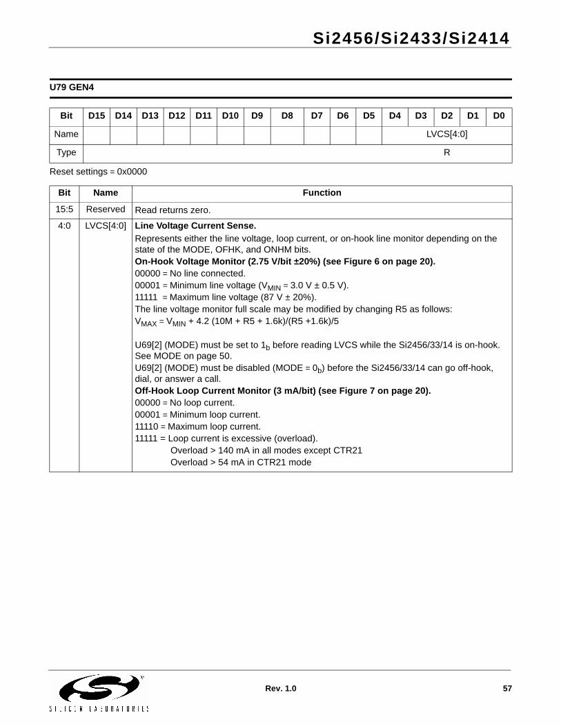
U79 GEN4
Bit D15 D14 D13 D12 D11 D10 D9 D8 D7 D6 D5 D4 D3 D2 D1 D0
Name LVCS[4:0]
Type R
Bit Name Function
15:5 Reserved Read returns zero.
4:0 LVCS[4:0] Line Voltage Current Sense.Represents either the line voltage, loop current, or on-hook line monitor depending on the state of the MODE, OFHK, and ONHM bits.On-Hook Voltage Monitor (2.75 V/bit ±20%) (see Figure 6 on page 20).00000 = No line connected.00001 = Minimum line voltage (VMIN = 3.0 V ± 0.5 V).11111 = Maximum line voltage (87 V ± 20%).The line voltage monitor full scale may be modified by changing R5 as follows:VMAX = VMIN + 4.2 (10M + R5 + 1.6k)/(R5 +1.6k)/5
U69[2] (MODE) must be set to 1b before reading LVCS while the Si2456/33/14 is on-hook. See MODE on page 50. U69[2] (MODE) must be disabled (MODE = 0b) before the Si2456/33/14 can go off-hook, dial, or answer a call.Off-Hook Loop Current Monitor (3 mA/bit) (see Figure 7 on page 20).00000 = No loop current.00001 = Minimum loop current.11110 = Maximum loop current.11111 = Loop current is excessive (overload).
Overload > 140 mA in all modes except CTR21Overload > 54 mA in CTR21 mode
Si2456/Si2433/Si2414
58 Rev. 1.0
Reset settings = 0x0000
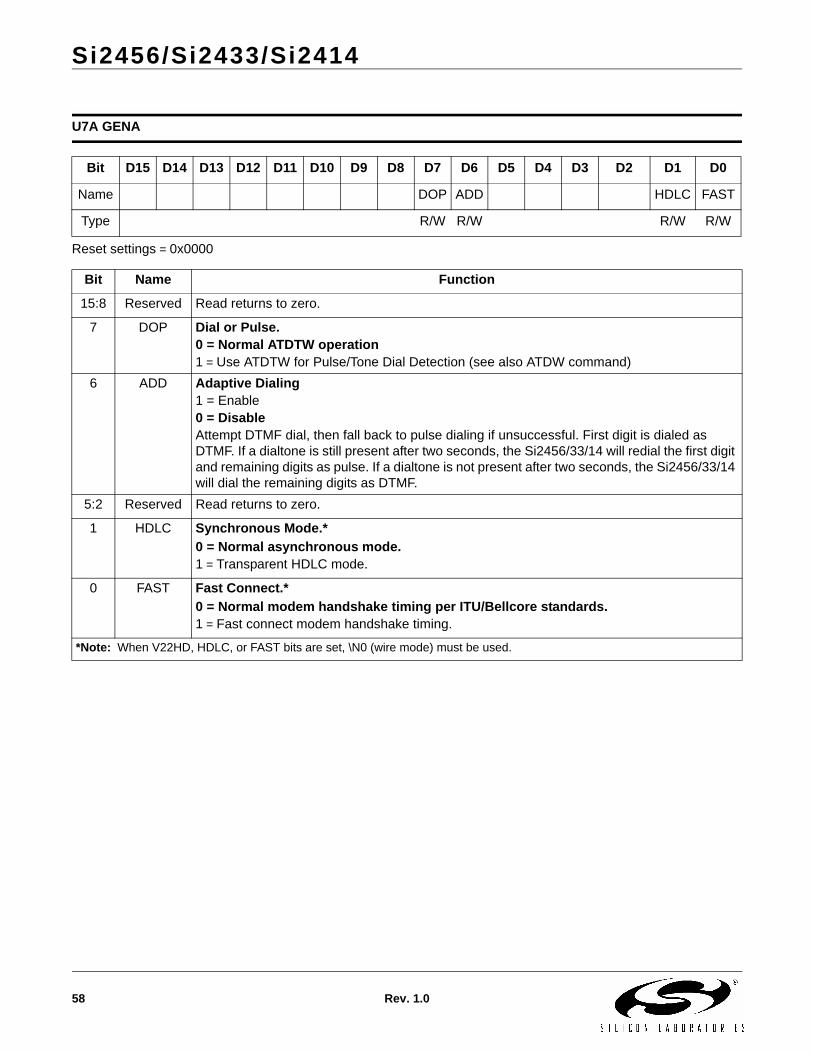
U7A GENA
Bit D15 D14 D13 D12 D11 D10 D9 D8 D7 D6 D5 D4 D3 D2 D1 D0
Name DOP ADD HDLC FAST
Type R/W R/W R/W R/W
Bit Name Function
15:8 Reserved Read returns to zero.
7 DOP Dial or Pulse.0 = Normal ATDTW operation1 = Use ATDTW for Pulse/Tone Dial Detection (see also ATDW command)
6 ADD Adaptive Dialing1 = Enable0 = DisableAttempt DTMF dial, then fall back to pulse dialing if unsuccessful. First digit is dialed as DTMF. If a dialtone is still present after two seconds, the Si2456/33/14 will redial the first digit and remaining digits as pulse. If a dialtone is not present after two seconds, the Si2456/33/14 will dial the remaining digits as DTMF.
5:2 Reserved Read returns to zero.
1 HDLC Synchronous Mode.*0 = Normal asynchronous mode.1 = Transparent HDLC mode.
0 FAST Fast Connect.*0 = Normal modem handshake timing per ITU/Bellcore standards.1 = Fast connect modem handshake timing.
*Note: When V22HD, HDLC, or FAST bits are set, \N0 (wire mode) must be used.
Si2456/Si2433/Si2414
Rev. 1.0 59
Reset settings = 0x0000
Reset settings = 0x0000
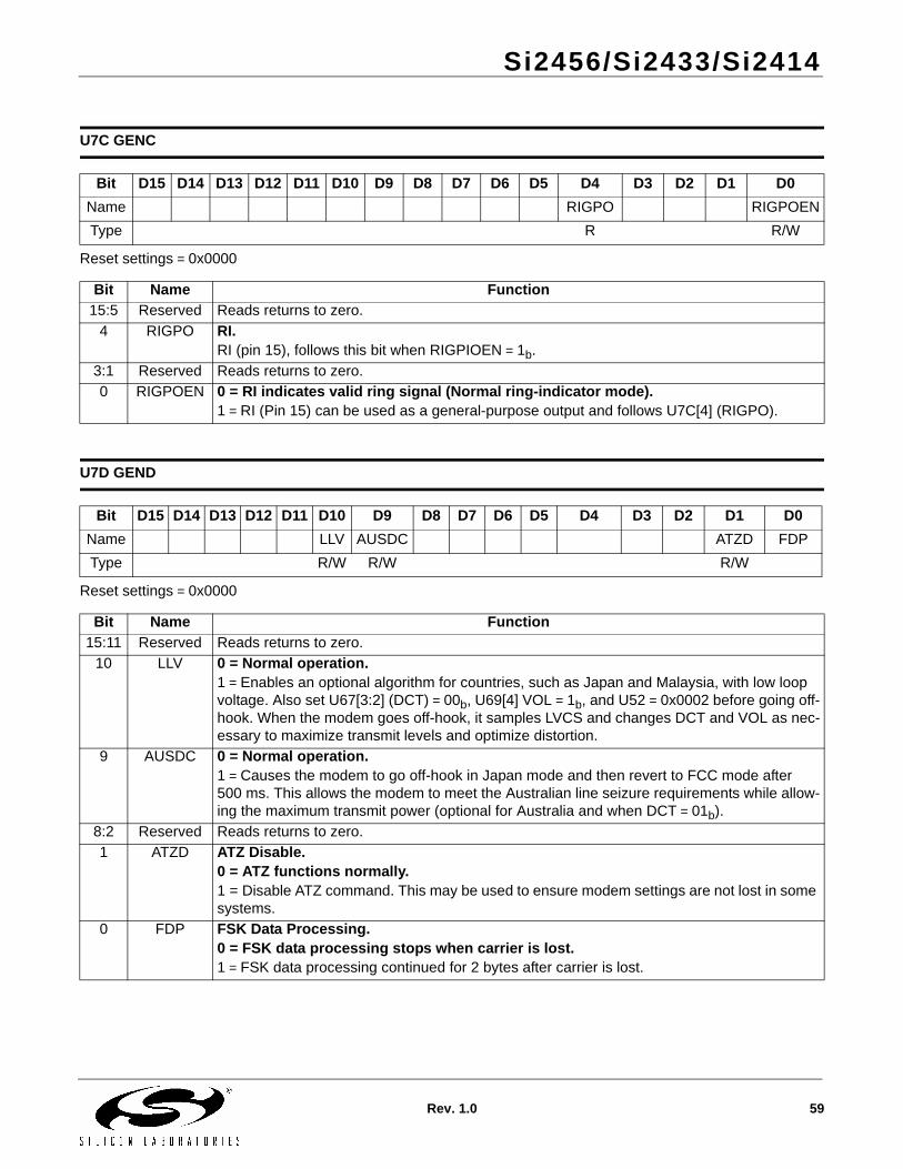
U7C GENC
Bit D15 D14 D13 D12 D11 D10 D9 D8 D7 D6 D5 D4 D3 D2 D1 D0Name RIGPO RIGPOENType R R/W
Bit Name Function15:5 Reserved Reads returns to zero.
4 RIGPO RI.RI (pin 15), follows this bit when RIGPIOEN = 1b.
3:1 Reserved Reads returns to zero.0 RIGPOEN 0 = RI indicates valid ring signal (Normal ring-indicator mode).
1 = RI (Pin 15) can be used as a general-purpose output and follows U7C[4] (RIGPO).
U7D GEND
Bit D15 D14 D13 D12 D11 D10 D9 D8 D7 D6 D5 D4 D3 D2 D1 D0Name LLV AUSDC ATZD FDPType R/W R/W R/W
Bit Name Function15:11 Reserved Reads returns to zero.
10 LLV 0 = Normal operation.1 = Enables an optional algorithm for countries, such as Japan and Malaysia, with low loop voltage. Also set U67[3:2] (DCT) = 00b, U69[4] VOL = 1b, and U52 = 0x0002 before going off-hook. When the modem goes off-hook, it samples LVCS and changes DCT and VOL as nec-essary to maximize transmit levels and optimize distortion.
9 AUSDC 0 = Normal operation.1 = Causes the modem to go off-hook in Japan mode and then revert to FCC mode after 500 ms. This allows the modem to meet the Australian line seizure requirements while allow-ing the maximum transmit power (optional for Australia and when DCT = 01b).
8:2 Reserved Reads returns to zero.1 ATZD ATZ Disable.
0 = ATZ functions normally.1 = Disable ATZ command. This may be used to ensure modem settings are not lost in some systems.
0 FDP FSK Data Processing.0 = FSK data processing stops when carrier is lost.1 = FSK data processing continued for 2 bytes after carrier is lost.
Si2456/Si2433/Si2414
60 Rev. 1.0
Parallel Interface Registers
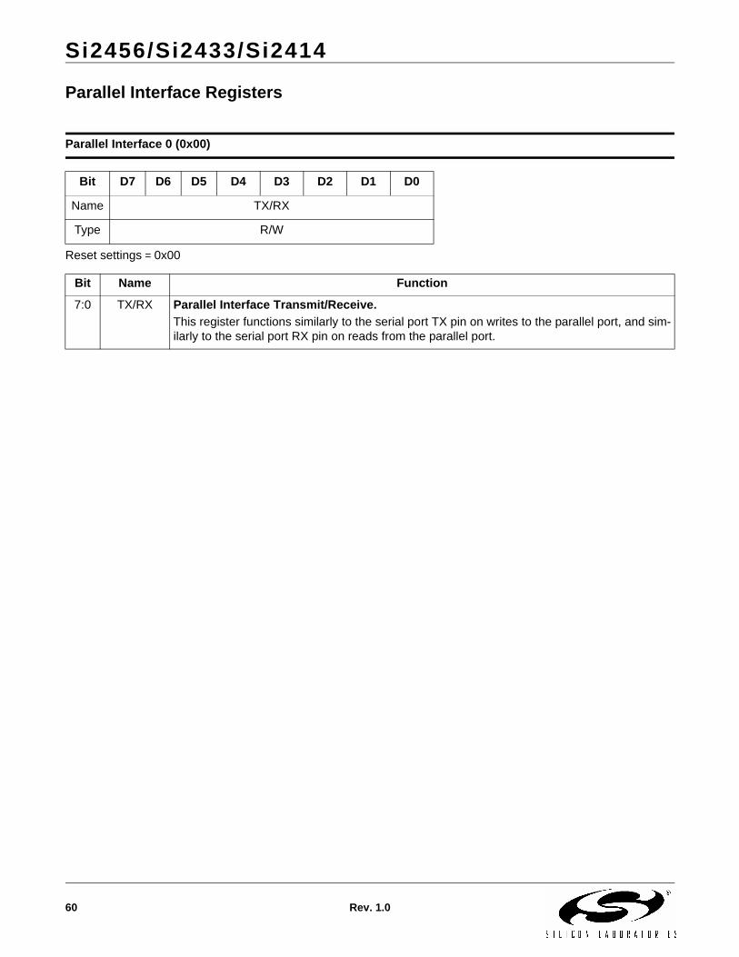
Reset settings = 0x00
Parallel Interface 0 (0x00)
Bit D7 D6 D5 D4 D3 D2 D1 D0
Name TX/RX
Type R/W
Bit Name Function
7:0 TX/RX Parallel Interface Transmit/Receive.This register functions similarly to the serial port TX pin on writes to the parallel port, and sim-ilarly to the serial port RX pin on reads from the parallel port.
Si2456/Si2433/Si2414
Rev. 1.0 61
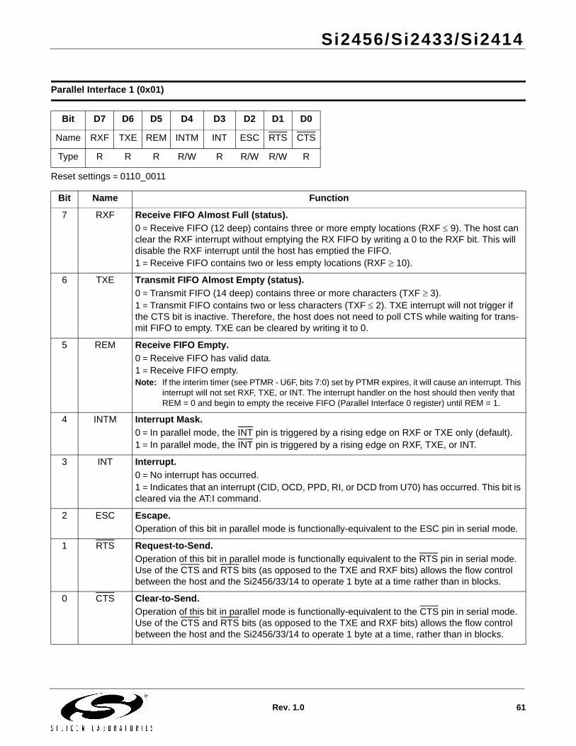
Reset settings = 0110_0011
Parallel Interface 1 (0x01)
Bit D7 D6 D5 D4 D3 D2 D1 D0
Name RXF TXE REM INTM INT ESC RTS CTS
Type R R R R/W R R/W R/W R
Bit Name Function
7 RXF Receive FIFO Almost Full (status).0 = Receive FIFO (12 deep) contains three or more empty locations (RXF ≤ 9). The host can clear the RXF interrupt without emptying the RX FIFO by writing a 0 to the RXF bit. This will disable the RXF interrupt until the host has emptied the FIFO.1 = Receive FIFO contains two or less empty locations (RXF ≥ 10).
6 TXE Transmit FIFO Almost Empty (status).0 = Transmit FIFO (14 deep) contains three or more characters (TXF ≥ 3).1 = Transmit FIFO contains two or less characters (TXF ≤ 2). TXE interrupt will not trigger if the CTS bit is inactive. Therefore, the host does not need to poll CTS while waiting for trans-mit FIFO to empty. TXE can be cleared by writing it to 0.
5 REM Receive FIFO Empty.0 = Receive FIFO has valid data.1 = Receive FIFO empty.Note: If the interim timer (see PTMR - U6F, bits 7:0) set by PTMR expires, it will cause an interrupt. This
interrupt will not set RXF, TXE, or INT. The interrupt handler on the host should then verify that REM = 0 and begin to empty the receive FIFO (Parallel Interface 0 register) until REM = 1.
4 INTM Interrupt Mask.0 = In parallel mode, the INT pin is triggered by a rising edge on RXF or TXE only (default).1 = In parallel mode, the INT pin is triggered by a rising edge on RXF, TXE, or INT.
3 INT Interrupt.0 = No interrupt has occurred.1 = Indicates that an interrupt (CID, OCD, PPD, RI, or DCD from U70) has occurred. This bit is cleared via the AT:I command.
2 ESC Escape.Operation of this bit in parallel mode is functionally-equivalent to the ESC pin in serial mode.
1 RTS Request-to-Send.Operation of this bit in parallel mode is functionally equivalent to the RTS pin in serial mode. Use of the CTS and RTS bits (as opposed to the TXE and RXF bits) allows the flow control between the host and the Si2456/33/14 to operate 1 byte at a time rather than in blocks.
0 CTS Clear-to-Send.Operation of this bit in parallel mode is functionally-equivalent to the CTS pin in serial mode. Use of the CTS and RTS bits (as opposed to the TXE and RXF bits) allows the flow control between the host and the Si2456/33/14 to operate 1 byte at a time, rather than in blocks.
Si2456/Si2433/Si2414
62 Rev. 1.0
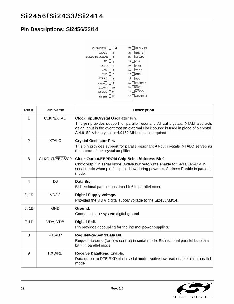
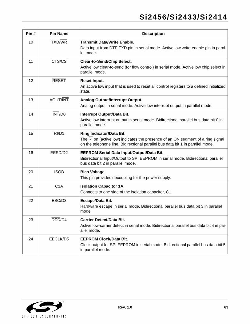
Pin Descriptions: Si2456/33/14
Pin # Pin Name Description
1 CLKIN/XTALI Clock Input/Crystal Oscillator Pin.This pin provides support for parallel-resonant, AT-cut crystals. XTALI also actsas an input in the event that an external clock source is used in place of a crystal.A 4.9152 MHz crystal or 4.9152 MHz clock is required.
2 XTALO Crystal Oscillator Pin.This pin provides support for parallel-resonant AT-cut crystals. XTALO serves asthe output of the crystal amplifier.
3 CLKOUT/EECS/A0 Clock Output/EEPROM Chip Select/Address Bit 0.Clock output in serial mode. Active low read/write enable for SPI EEPROM in serial mode when pin 4 is pulled low during powerup. Address Enable in parallel mode.
4 D6 Data Bit.Bidirectional parallel bus data bit 6 in parallel mode.
5, 19 VD3.3 Digital Supply Voltage.Provides the 3.3 V digital supply voltage to the Si2456/33/14.
6, 18 GND Ground.Connects to the system digital ground.
7,17 VDA, VDB Digital Rail.Pin provides decoupling for the internal power supplies.
8 RTS/D7 Request-to-Send/Data Bit.Request-to-send (for flow control) in serial mode. Bidirectional parallel bus data bit 7 in parallel mode.
9 RXD/RD Receive Data/Read Enable.Data output to DTE RXD pin in serial mode. Active low read enable pin in parallel mode.
1
23
45
67
89
10
1112 13
14
1516
1718
1920
21
2223
24CLKIN/XTALI
XTALOCLKOUT/EECS/AO
D6
VD3.3GND
VDA
RTS/D7
RXD/RDTXD/WRCTS/CS
RESET AOUT/INT
INT/DORI/D1EESD/D2
VDB
GNDVD3.3
C1A
ESC/D3DCD/D4
ISOB
EECLK/D5
Si2456/Si2433/Si2414
Rev. 1.0 63
10 TXD/WR Transmit Data/Write Enable.Data input from DTE TXD pin in serial mode. Active low write-enable pin in paral-lel mode.
11 CTS/CS Clear-to-Send/Chip Select.Active low clear-to-send (for flow control) in serial mode. Active low chip select in parallel mode.
12 RESET Reset Input.An active low input that is used to reset all control registers to a defined initialized state.
13 AOUT/INT Analog Output/Interrupt Output.Analog output in serial mode. Active low interrupt output in parallel mode.
14 INT/D0 Interrupt Output/Data Bit.Active low interrupt output in serial mode. Bidirectional parallel bus data bit 0 in parallel mode.
15 RI/D1 Ring Indicator/Data Bit.The RI on (active low) indicates the presence of an ON segment of a ring signal on the telephone line. Bidirectional parallel bus data bit 1 in parallel mode.
16 EESD/D2 EEPROM Serial Data Input/Output/Data Bit.Bidirectional Input/Output to SPI EEPROM in serial mode. Bidirectional parallel bus data bit 2 in parallel mode.
20 ISOB Bias Voltage.This pin provides decoupling for the power supply.
21 C1A Isolation Capacitor 1A.Connects to one side of the isolation capacitor, C1.
22 ESC/D3 Escape/Data Bit.Hardware escape in serial mode. Bidirectional parallel bus data bit 3 in parallel mode.
23 DCD/D4 Carrier Detect/Data Bit.Active low-carrier detect in serial mode. Bidirectional parallel bus data bit 4 in par-allel mode.
24 EECLK/D5 EEPROM Clock/Data Bit.Clock output for SPI EEPROM in serial mode. Bidirectional parallel bus data bit 5 in parallel mode.
Pin # Pin Name Description
Si2456/Si2433/Si2414
64 Rev. 1.0
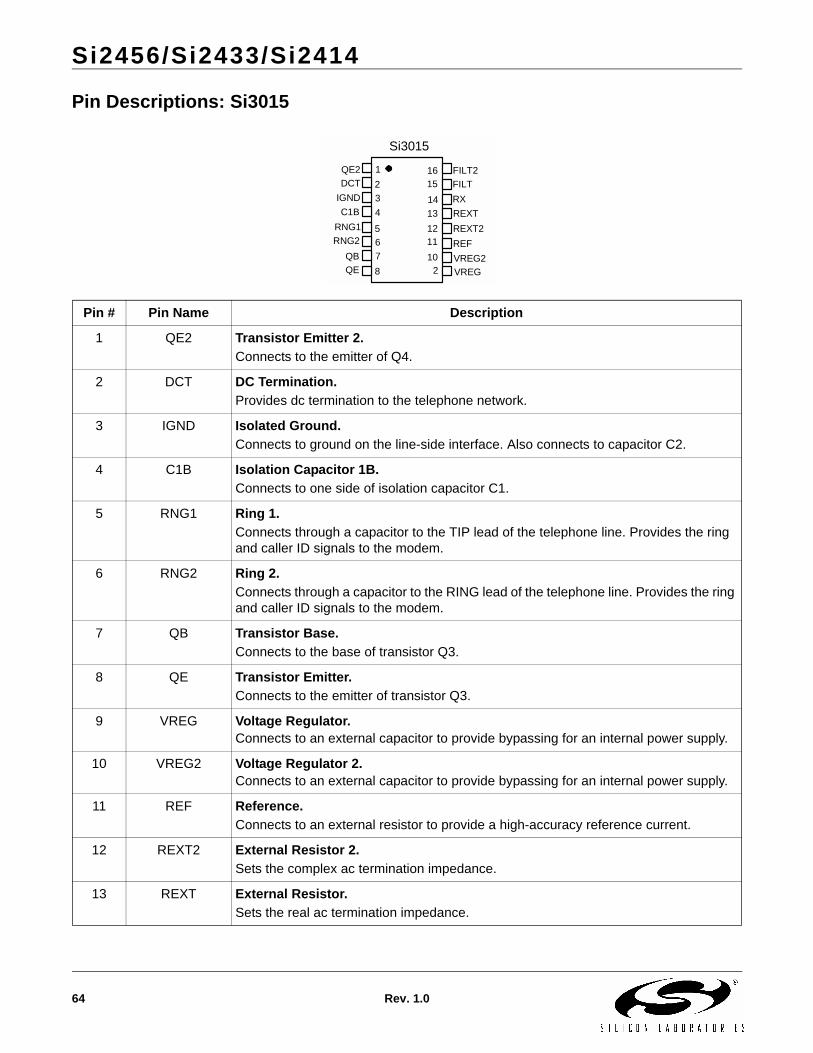
Pin Descriptions: Si3015
Pin # Pin Name Description
1 QE2 Transistor Emitter 2.Connects to the emitter of Q4.
2 DCT DC Termination.Provides dc termination to the telephone network.
3 IGND Isolated Ground.Connects to ground on the line-side interface. Also connects to capacitor C2.
4 C1B Isolation Capacitor 1B.Connects to one side of isolation capacitor C1.
5 RNG1 Ring 1.Connects through a capacitor to the TIP lead of the telephone line. Provides the ring and caller ID signals to the modem.
6 RNG2 Ring 2.Connects through a capacitor to the RING lead of the telephone line. Provides the ring and caller ID signals to the modem.
7 QB Transistor Base.Connects to the base of transistor Q3.
8 QE Transistor Emitter.Connects to the emitter of transistor Q3.
9 VREG Voltage Regulator.Connects to an external capacitor to provide bypassing for an internal power supply.
10 VREG2 Voltage Regulator 2.Connects to an external capacitor to provide bypassing for an internal power supply.
11 REF Reference.Connects to an external resistor to provide a high-accuracy reference current.
12 REXT2 External Resistor 2.Sets the complex ac termination impedance.
13 REXT External Resistor.Sets the real ac termination impedance.
QE22345678 2
10111213141516
DCTIGNDC1B
RNG1RNG2
QBQE VREG
VREG2REFREXT2REXTRXFILTFILT21
Si3015
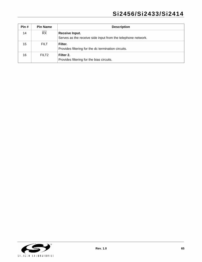
Si2456/Si2433/Si2414
Rev. 1.0 65
14 RX Receive Input.Serves as the receive side input from the telephone network.
15 FILT Filter.Provides filtering for the dc termination circuits.
16 FILT2 Filter 2.Provides filtering for the bias circuits.
Pin # Pin Name Description
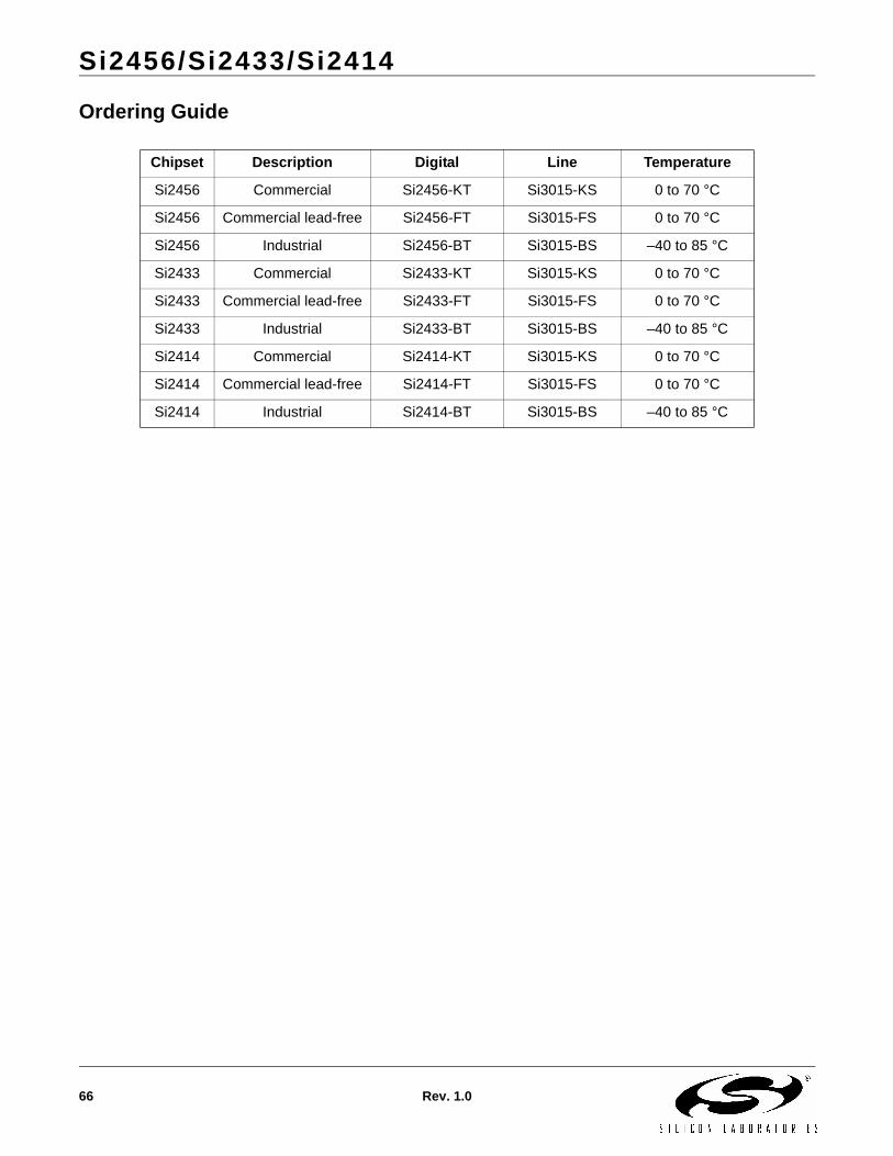
Si2456/Si2433/Si2414
66 Rev. 1.0
Ordering Guide
Chipset Description Digital Line Temperature
Si2456 Commercial Si2456-KT Si3015-KS 0 to 70 °C
Si2456 Commercial lead-free Si2456-FT Si3015-FS 0 to 70 °C
Si2456 Industrial Si2456-BT Si3015-BS –40 to 85 °C
Si2433 Commercial Si2433-KT Si3015-KS 0 to 70 °C
Si2433 Commercial lead-free Si2433-FT Si3015-FS 0 to 70 °C
Si2433 Industrial Si2433-BT Si3015-BS –40 to 85 °C
Si2414 Commercial Si2414-KT Si3015-KS 0 to 70 °C
Si2414 Commercial lead-free Si2414-FT Si3015-FS 0 to 70 °C
Si2414 Industrial Si2414-BT Si3015-BS –40 to 85 °C
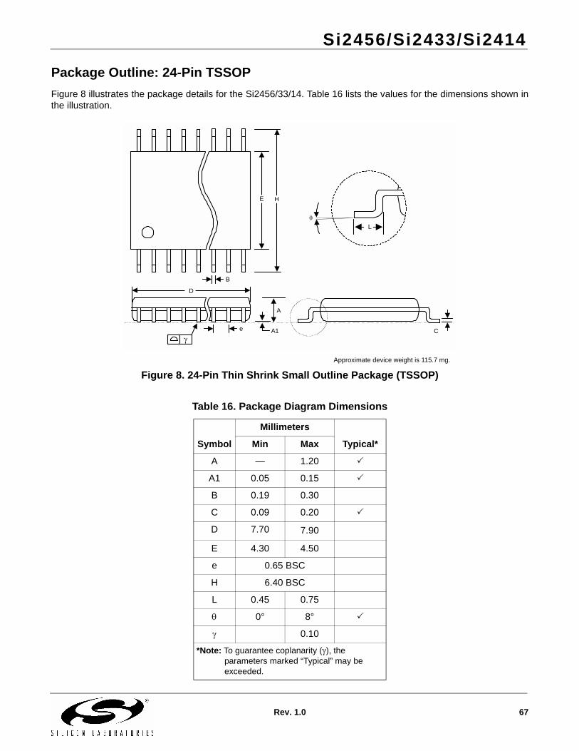
Si2456/Si2433/Si2414
Rev. 1.0 67
Package Outline: 24-Pin TSSOPFigure 8 illustrates the package details for the Si2456/33/14. Table 16 lists the values for the dimensions shown inthe illustration.
Figure 8. 24-Pin Thin Shrink Small Outline Package (TSSOP)
Table 16. Package Diagram Dimensions
Symbol
Millimeters
Typical*Min Max
A — 1.20 !
A1 0.05 0.15 !
B 0.19 0.30
C 0.09 0.20 !
D 7.70 7.90
E 4.30 4.50
e 0.65 BSC
H 6.40 BSC
L 0.45 0.75
θ 0° 8° !
γ 0.10
*Note: To guarantee coplanarity (γ), the parameters marked “Typical” may be exceeded.
Approximate device weight is 115.7 mg.
γ
E H
B
D
Lθ
C
A
A1e
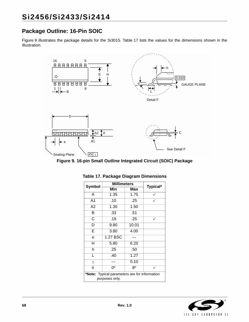
Si2456/Si2433/Si2414
68 Rev. 1.0
Package Outline: 16-Pin SOICFigure 9 illustrates the package details for the Si3015. Table 17 lists the values for the dimensions shown in theillustration.
Figure 9. 16-pin Small Outline Integrated Circuit (SOIC) Package
Table 17. Package Diagram Dimensions
Symbol Millimeters Typical*Min MaxA 1.35 1.75 !
A1 .10 .25 !
A2 1.30 1.50B .33 .51C .19 .25 !
D 9.80 10.01E 3.80 4.00e 1.27 BSC —H 5.80 6.20h .25 .50L .40 1.27γ — 0.10θ 0º 8º !
*Note: Typical parameters are for information purposes only.
E H
A1
B
C
h
L
θ
e
See Detail F
Detail F
A
16 9
81GAUGE PLANE
0.010
D
A2
Seating Plane γ
Si2456/Si2433/Si2414
Rev. 1.0 69
Document Change ListRevision 0.9 to Revision 1.0.! The Si2456/33/14 data sheet has changed
significantly since revision 0.9. In order to offer a simplified reference for customers, many of the detailed feature explanations have been moved to the Si2456/33/14 User’s Guide (“AN70: Si2456/Si2433/Si2414/Si2403 Modem Designer’s Guide”). Therefore, many of the following changes refer not only to this data sheet, but also to the new revision of AN70.
! Updated "Parallel Interface" on page 17.! Updated register, "Parallel Interface 1 (0x01)" on
page 61.! Added register, "U6F PTMR" on page 52.! Added "Autobaud" on page 17.! Added "V.29 Fast Connect" on page 18 and
associated AT commands.! Added "EEPROM Interface" on page 21.! Updated "Pin Assignments" on page 1, "Pin
Descriptions: Si2456/33/14" on page 62, and "Typical Application Schematic" on page 11 to include EEPROM support.
! Updated "Clocking/Low Power Modes" on page 18! Added &Pn, &Xn, &Dn, &G3, &G4, &T4, &T5, &T,
\T16, \T17, %B, %Vn, +GCI, and \N5 commands.! Added G modifier to ATD command! Added S-registers S40, S41, S42, S50 in Table 13.! Updated S-register S7 in Table 13! Added result codes 40–45 in Table 12! Updated Figure 8, “24-Pin Thin Shrink Small Outline
Package (TSSOP)”! Updated “Typical Application Schematic”.! Added AT2D bit (U7D, bit 2).! Removed Country-Specific Register Settings table.! Updated Table 14.! Updated Table 15.! Added -FT, -FS lead-free commercial-grade device
ordering option.! Changed Note 3 in "Bill of Materials: Si2456/33/14
Chipset" on page 12.! Removed U-register IO1 (U71)! Added U-registers U7C and U7D! Removed CCAD bit (U40, bit 9)! Added LCN bit (U47, bit 0)! Added RFWE bit (U69, bit 1)! Removed RST bit (U6E, bit 4)! Moved AOUT schematic and component values
table to AN70.! Updated Pullup Resistance Pins in Table 3.