12th electronics packaging research consortium (eprc … 12 - project proposal... · project...
TRANSCRIPT

Project Proposal Presentation
12th Electronics Packaging Research Consortium (EPRC 12) Industry Forum
15 August 2012

Property of Institute of Microelectronics. Copyright ® 2012
IME’s Advanced Packaging Strategic FocusBroad base capabilities to engage industry partners
Advanced Packaging
at IME
Advanced Packaging/2.
5D/3DIC
Si Photonics
Bio Electronics
Ruggedized Electronics
Green Electronics
GaN on Si Power
Electronics
Sensors Actuators and Microsystems
Miniaturized Medical Devices
• Integrated Fiber Coupling• Low-Cost MEMS-assisted
Passive/Active Packaging & Assembly
• Flip-Chip, micro-bumping & 2.5D Platform for O/E IC
• Thermal aware Packaging Innovation
• Nanowire Integration,• Heterogeneous integration
(MEMs, Logic, Memory , Analog/RF, Photonics)
• Biosensor packaging• Microfluidics-integrated
biosensor array• TSV biosensor array
• Over 300oC / 30 kpsi reliability • Novel interconnection and
encapsulation materials >300oC• MEMS sensor hermetic sealing for
harsh environment
• Chip on Flexible Substrate (chip size < 250 um x 250 um)
• Biocompatible Encapsulation for long term implantation
• Flip Chip for MEMS structure
• Vacuum/Hermetic WLP with TSV
• Thin Film Encapsulation• Low Cost Solutions - MEMS-
ASIC Integration
• Low Cost, small size, high-reliable module packaging;
• Reduced parasitics (e.g., Inductance) for higher efficiency;
• Integrated thermal management solution
• 3D Logic on memory stacking• Heterogeneous integration (TSI)• Fine pitch interconnection• Cu wire bonding

Collaboration with IndustryBenefits of Working in Consortium
• Increase R&D resource pool with shared R&D cost
• Development of advanced technologies & know-how
• Knowledge & data base creation
• Worldwide networking
• Product development
• Competency development
• Manufacturing
• Enhanced competencies & competitive edge
• Better products / services• Business Opportunities
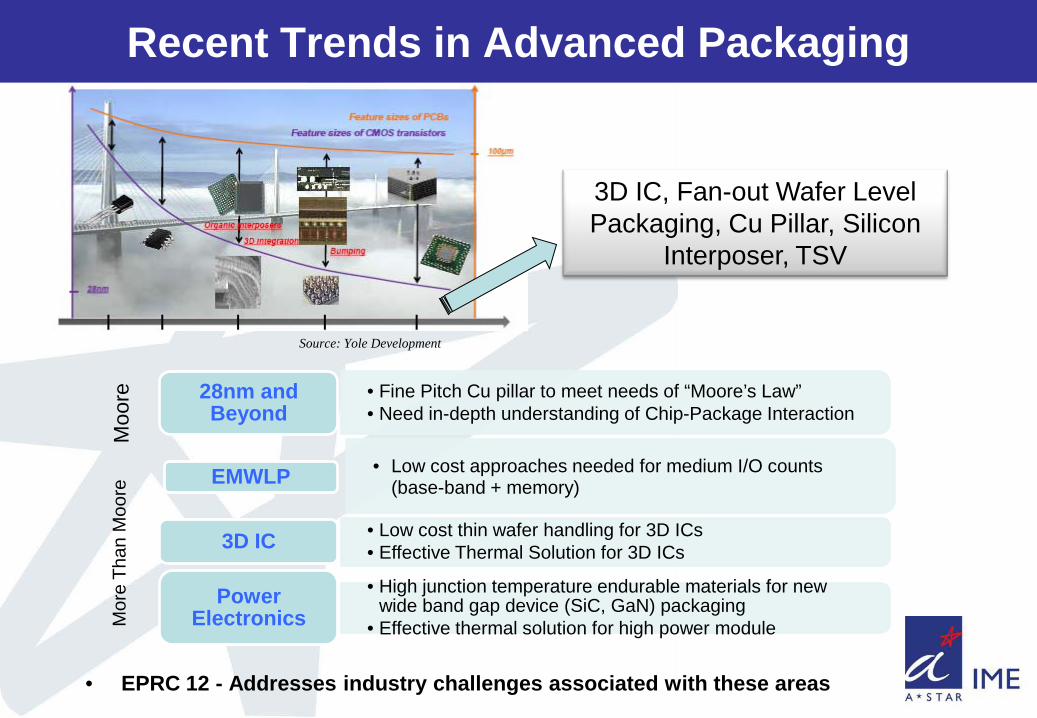
Recent Trends in Advanced Packaging
• EPRC 12 - Addresses industry challenges associated with these areas
• Fine Pitch Cu pillar to meet needs of “Moore’s Law”• Need in-depth understanding of Chip-Package Interaction
28nm and Beyond
• Low cost approaches needed for medium I/O counts (base-band + memory) EMWLP
• Low cost thin wafer handling for 3D ICs• Effective Thermal Solution for 3D ICs3D IC
• High junction temperature endurable materials for new wide band gap device (SiC, GaN) packaging
• Effective thermal solution for high power module
Power Electronics
Moo
reM
ore
Than
Moo
re
3D IC, Fan-out Wafer Level Packaging, Cu Pillar, Silicon
Interposer, TSV
Source: Yole Development

Cu Pillar Interconnect and CPI on Advanced Cu Low K Chip• Chip-Packaging-Interaction (CPI) characterization for advanced ultra low K chip with Cu pillar interconnect
Embedded Cooling Solution for 3D Stack Chip• Development and characterization of embedded thermoelectric cooling system in die-stack for next generation of 2.5D/3D devices
Development of Power Module for Device Temperature over 220°C• Development and characterization of power semiconductor packages for high junction temperature endurable (>220°C) solutions for next generation devices
Thin Wafer Handling for 3D Packaging• Develop stable and robust backside TSV revealing process flow with both TBDB and carrier-less approach
3D-Embedded WLP•Develop embedded wafer level packaging for low to high I/O application
• 5 Projects are formulated based on industry needs and survey results• Projects Schedule (proposed) : Dec 2012 – May 2014 (18 months)
EPRC 12 – Projects Overview
Please see individual project file attached.

Page 6
IME: Confidential and Proprietary
Project Membership Participations
&Follow up
Communication
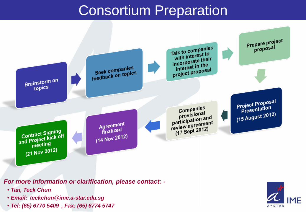
Consortium Preparation
For more information or clarification, please contact: -• Tan, Teck Chun• Email: [email protected]• Tel: (65) 6770 5409 , Fax: (65) 6774 5747

Cu Pillar Interconnect and CPI on Advanced Cu Low K Chip• Chip-Packaging-Interaction (CPI) characterization for advanced ultra low K chip with Cu pillar interconnect
Embedded Cooling Solution for 3D Stack Chip• Development and characterization of embedded thermoelectric cooling system in die-stack for next generation of 2.5D/3D devices
Development of Power Module for Device Temperature over 220°C• Development and characterization of power semiconductor packages for high junction temperature endurable (>220°C) solutions for next generation devices
Thin Wafer Handling for 3D Packaging• Develop stable and robust backside TSV revealing process flow with both TBDB and carrier-less approach
3D-Embedded WLP•Develop embedded wafer level packaging for low to high I/O application
• 5 Projects are formulated based on industry needs and survey results• Projects Schedule (proposed) : Dec 2012 – May 2014 (18 months)
EPRC 12 – Projects Overview

2-Tier Membership Structure
• Core membership is S$80,000/= per project• Associate membership is S$60,000/= per project

Project Execution & Communication
• Execution– A project team will be formed for each project– The members in the project review meeting will
direct the EPRC 12 efforts to meet the project targets & review its progress.
– The members will have the choice to participate in the experiments and contribute to the success of the project.
• Communication– Working meeting and progress review meeting :
approx. 6 weekly

Responsibility of IME & Consortium Members• IME:
– To conduct research on the Project with the participation of the Consortium members
– To co-ordinate activities relating to the Project, including organising the Consortium meetings for the purpose of updating members on a regular basis
– To report on the findings of the research work and to keep the Consortium members informed
• Consortium members:– To actively participate in the Project as and when required by the
Consortium for the purpose of carrying out and completing the Project
– To assist in contacting material suppliers as and when required by the Consortium to carry out the Project
– To provide inputs that are required for the formulation of the Project work scope and for the purpose of carrying out the Project

Provisional Participation
End of Presentation