10811 a&b quartz crystal oscillator - hp archivehparchive.com/manuals/hp-10811ab-manual.pdf ·...
TRANSCRIPT

Model 10811A/B
Errata
Title & Document Type: 10811A/B Quartz Crystal Oscillator Operating &
Service Manual (V2) Manual Part Number: 10811-90002 Serial Prefixes: 2028 Revision Date: August 1980
HP References in this Manual
This manual may contain references to HP or Hewlett-Packard. Please note that Hewlett-Packard's former test and measurement, semiconductor products and chemical analysis businesses are now part of Agilent Technologies.
Changes to this Manual No changes have been made to this manual, with the exception of correcting the odd spelling and grammatical errors. In some places original photographs may be replaced or augmented with modern digital photographs. All pages are scan at 600 DPI and in some cases (schematics) scaled down to fit 8½x11 page. If you wish to print on 11x17 or larger just print the page and scale to fit.
About this Manual This manual is reproduced from scans of an original document, which is then converted using my own custom designed OCR software, and then edited in Microsoft® Word 2003. This means that what you see here is not a scan of a scan/copy with text overlays. OCR errors may exist and as such the user of this document should take care and use common sense when referencing this documentation.
Copyright Notice This documentation is © Copyright 1980 Hewlett Packard and © Copyright 2007, Jack Hudler, [email protected]. Permission to use and redistribute this documentation for non-commercial and internal corporate purposes is hereby granted, free of charge. Any redistribution of this documentation or its derivates must include this copyright notice. You may not sell this documentation or its derivations without written consent. You may modify this documentation as necessary, but you may not sell derivative works based on it. You may include this documentation with the equipment/hardware on which it is used for the purposes of selling the equipment/hardware. If you advertise that a copy of this documentation is included in the sale, you must state that is for “Free”. Meaning if you want to gratuitously toss in a copy of the manual on an eBay sale, it’s ok with me as long as you state it’s for free. No you can’t sell a digital archive of manuals and say it includes a free copy of this documentation. You must give it away with equipment. I think you get the spirit of the copyright; it takes a lot of hours to scan and replicate a manual. I just want this used in the spirit in which is it given. Agilent if you have questions or wish to include this in your archive, please email me.

Model 10811A/B
Page Intentionally Left Blank
Model 10811A/B

Model 10811A/B
10811A/B QUARTZ CRYSTAL OSCILLATOR
OPERATING AND SERVICE MANUAL
SERIAL PREFIX: 2028
This manual applies to Hewlett-Packard Model 10811A/B Oscillators with serial prefix number 2028. Also covers oscillators with HP Part Numbers 10811-60101 and 10811-60105.
OTHER SERIAL PREFIXES
For serial prefixes above 2028, a "Manual Change" sheet is included with this manual.
First Edition - August 1980
©Copyright 1980 by
HEWLETT-PACKARD COMPANY 5301 Stevens Creek Blvd.
Santa Clara, CA 95050
All Rights Reserved
MANUAL PART NUMBER 10811-90002 Microfiche Part Number 10811-90003

Model 10811A/B
TABLE OF CONTENTS
I. GENERAL INFORMATION ..................................................................................2 1-1. INTRODUCTION....................................................................................................2 1-4. SPECIFICATIONS .................................................................................................2 1-6. SAFETY CONSIDERATIONS................................................................................2 1-8. INSTRUMENTS COVERED BY THIS MANUAL...................................................2 1-13. DESCRIPTION.......................................................................................................4 1-19. HP Part Number 10811-60101 and 10811-60105 ..........................................4 1-22. RECOMMENDED TEST EQUIPMENT .................................................................4
II. INSTALLATION..................................................................................................6 2-1. INTRODUCTION....................................................................................................6 2-3. INITIAL INSPECTION............................................................................................6 2-5. PREPARATION FOR USE ....................................................................................6 2-6. Power Requirements.......................................................................................6 2-10. Single Source Regulated Power Supply .........................................................7 2-12. ELECTRONIC FREQUENCY CONTROL (EFC)...................................................7 2-16. 10 MHz FREQUENCY OUTPUT SIGNAL ......................................................7 2-18. OVEN MONITOR OUTPUT...................................................................................8 2-20. MATING CONNECTORS AND MOUNTING .........................................................8 2-23. INSTALLATION INSTRUCTIONS...................................................................9 2-25. INSTALLATION INSTRUCTIONS (HP INSTRUMENT) ......................................10 2-28. OPERATING ENVIRONMENT ............................................................................10 2-34. STORAGE AND SHIPMENT ...............................................................................11 2-35. Environment ..................................................................................................11 2-37. PACKAGING........................................................................................................11 2-38. Original Packaging ........................................................................................11 2-40. Other Packaging............................................................................................11
III. OPERATION ....................................................................................................12 3-1. INTRODUCTION..................................................................................................12 3-3. BASIC POWER-UP DESCRIPTION....................................................................12 3-7. FREQUENCY ADJUSTMENT .............................................................................12 3-9. FREQUENCY ADJUSTMENT PROCEDURE .....................................................12 3-10. ACCURACY VS ADJUSTMENT INTERVAL .......................................................13
IV. OPERATIONAL VERIFICATION ........................................................................16 4-1. INTRODUCTION..................................................................................................16 4-3. OPERATIONAL VERIFICATION .........................................................................16 4-5. EQUIPMENT REQUIRED....................................................................................16 4-7. TEST RECORD ...................................................................................................16 4-13. OPTIONAL CONTROLLERS AND COUNTERS.................................................21 4-14. Optional Controllers.......................................................................................21 4-16. Optional Counters..........................................................................................22
V. ADJUSTMENTS ...............................................................................................25 5-1. INTRODUCTION..................................................................................................25 5-3. EQUIPMENT REQUIRED....................................................................................25 5-5. FACTORY SELECTED COMPONENTS.............................................................25 5-7. ADJUSTMENT LOCATION .................................................................................25 5-9. SAFETY CONSIDERATIONS..............................................................................25 5-11. OSCILLATOR FREQUENCY ADJUSTMENT .....................................................25 5-13. Offset Calculation: .........................................................................................26 5-14. OUTPUT AMPLITUDE ADJUSTMENT ...............................................................27

Model 10811A/B
VI. REPLACEABLE PARTS.................................................................................... 29 6-1. INTRODUCTION..................................................................................................29 6-3. ORDERING INFORMATION ...............................................................................29 6-5. HP PART NUMBER ORGANIZATION ................................................................29 6-7. Component Parts and Materials ..........................................................................30 6-10. GENERAL USAGE PARTS .................................................................................31 6-12. Specific Instrument Parts .....................................................................................31 6-14. Factory Selected Parts.........................................................................................31 6-20. REPLACEABLE PARTS LIST LAYOUT..............................................................31
VII. MANUAL CHANGES ........................................................................................ 37 7-1. INTRODUCTION..................................................................................................37 7-3. MANUAL CHANGES ...........................................................................................37 7-5. NEWER INSTRUMENTS.....................................................................................37
VIII. SERVICE.................................................................................................... 39 8-1. INTRODUCTION..................................................................................................39 8-3. SCHEMATIC DIAGRAM SYMBOLS AND REFERENCE DESIGNATORS ........39 8-5. REFERENCE DESIGNATORS............................................................................39 8-6. Theory of Operation.......................................................................................39 8-8. OVERALL BLOCK DIAGRAM THEORY .............................................................39 8-13. MAIN OSCILLATOR THEORY OF OPERATION................................................42 8-18. ELECTRONIC FREQUENCY CONTROL (EFC).................................................43 8-20. AUTOMATIC GAIN CONTROL (AGC) ................................................................44 8-23. RF OUTPUT IMPEDANCE MATCHING AND OUTPUT BUFFER......................45 8-25. VOLT AGE REFERENCES (5.7V AND 6.4V) .....................................................45 8-27. OVEN HEATER AND CONTROLLER THEORY.................................................46 8-35. PRECISION VOLTAGE REFERENCE................................................................47 8-37. OVEN CONTROLLER TURN-ON CURRENT LIMITING ....................................47 8-39. HEATER TRANSISTOR BALANCE ....................................................................48 8-41. REPAIR AND TROUBLESHOOTING..................................................................49 8-42. Inspection ......................................................................................................49 8-44. REPAIR................................................................................................................49 8-45. Printed Circuit Component Replacement ......................................................49 8-47. Replacing Integrated Circuits ........................................................................49 8-50. TROUBLESHOOTING.........................................................................................50 8-57. DISASSEMBLY FOR TROUBLESHOOTING AND REPAIR...............................51 8-61. SPECIAL TEST CONNECTOR FOR 10811A .....................................................52 8-65. SPECIAL CABLE FOR THE 10811B...................................................................53 8-67. SPECIAL PARTS REPLACEMENT CONSIDERATIONS ...................................53 8-69. OVEN CONTROLLER TROUBLESHOOTING....................................................55 8-70. General ..........................................................................................................55 8-74. Normal Operation ..........................................................................................56 8-76. TROUBLESHOOTING.........................................................................................56 8-80. Troubleshooting Cautions..............................................................................56 8-82. Flex Damage .................................................................................................56 8-84. OSCILLATOR TROUBLESHOOTING.................................................................58 8-86. NORMAL OPERATION .......................................................................................58 8-88. OSCILLATOR TROUBLESHOOTING TECHNIQUES ........................................58 8-92. TROUBLESHOOTING INFORMATION...............................................................59

Model 10811A/B
LIST OF TABLES Table 1-1. Specifications Table ..............................................................................................................3 Table 1-2. Recommended Test Equipment............................................................................................5 Table 2-1. Input Voltages/Voltage Coefficients ......................................................................................6 Table 3-1. Accuracy vs Adjustment ......................................................................................................14 Table 4-1. Operational Verification Descriptions ..................................................................................17 Table 4-2. Operation Verification Procedure ........................................................................................18 Table 4-3. 5316A Program Codes........................................................................................................22 Table 4-4. Operational Verification Record ..........................................................................................24 Table 6-1. Replaceable Parts ...............................................................................................................32 Table 6-1. Replaceable Parts (Continued) ...........................................................................................34 Table 6-2. Manufacturers Code List .....................................................................................................35 Table 8-1. Temperature Set Resistor List. ...........................................................................................54 Table 8-2. Oven Controller Troubleshooting Tree................................................................................57 Table 8-3. Oven Circuit Voltages·.........................................................................................................61 Table 8-4. Oscillator Section Normal Voltages (see Notes 1, 2, 3)......................................................61
LIST OF FIGURES
Figure 1-1. 10811A and 108118 Oscillators...........................................................................................1 Figure 2-1. Single Source Regulated Power Supply ..............................................................................7 Figure 2-3. 10811A Supply and Output Connections.............................................................................8 Figure 2-4. 10811B Supply and Output Connections.............................................................................9 Figure 2-5. Mechanical Mounting Dimensions .....................................................................................10 Figure 3-1. Oscillator Adjustment Set-Up.............................................................................................13 Figure 4-1. BASIC Program..................................................................................................................21 Figure 4-2. HPL Program .....................................................................................................................21 Figure 5-1. Oscillator Adjustment Setup...............................................................................................26 Figure 5-2. 10811A Amplitude Adjustment Set-up ...............................................................................27 Figure 5-3. 108118 Amplitude Adj Set-up ............................................................................................28 Figure 8-1. Schematic Diagram Notes .................................................................................................40 Figure 8-2. 10811A/B Overall Block Diagram ......................................................................................41 Figure 8-3A. Basic Colpitts- Type Oscillator.........................................................................................42 Figure 8-3B. Main Oscillator Schematic Design...................................................................................42 Figure 8-4. Mode Suppression .............................................................................................................43 Figure 8-5. Frequency Tuning Circuit ...................................................................................................43 Figure 8-6. EFC ....................................................................................................................................44 Figure 8-7. Automatic Gain Control (AGC)...........................................................................................44 Figure 8-8. Output Amplifiers................................................................................................................45 Figure 8-9. Voltage References............................................................................................................46 Figure 8-10. Oven Control Circuits .......................................................................................................47 Figure 8-11. Turn-on Current Limit Circuit............................................................................................48 Figure 8-12. Heater Transistor Balance Circuit. ...................................................................................48 Figure 8-13. 10811A/B Special Test Connector...................................................................................52 Figure 8-14. Oven Controller Block Diagram .......................................................................................55 Figure 8-15. Oven Controller Schematic Diagram ...............................................................................64

Model 10811A/B
PREFACE This manual is designed to present the information required by the user to effectively operate and maintain the 10811A/B Quartz Crystal Oscillator. In limiting the depth of coverage of this manual, a certain amount of previous knowledge on the part of the reader must be assumed. A variety of additional related documentation is available. These materials address the specific areas of interest, and should be used whenever necessary to supplement this manual. Users unfamiliar with precision time keeping and frequency standards, for example, may wish to refer to the 10811A/B Documentation Map for further information. The following references can provide additional information about the theory and use of precision frequency sources and quartz oscillators.
1. Application Note 52-1 Hewlett-Packard Fundamentals of Time and Frequency Standards.
2. Application Note 52-2 Hewlett-Packard Time Keeping and Frequency Calibration.
3. Application Note 200-2 Hewlett-Packard Fundamentals of Quartz Oscillators.
4. U.S. National Bureau of Standards, Monograph 140, Time and Frequency Theory and Fundamentals available from:
Superintendent of Documents U. S. Government Printing Office Washington, D.C. 20402
5. In 1990 the NIST replaced the Monograph 140 document with this interim collection of documents NIST/TN1-339 or visit time NIST Time and Frequency Publication Database.
The 10811A/B Quartz Crystal Oscillator has two manuals available. The Operating Instruction
Manual is supplied with the oscillator and is intended for the user that desires only operating information. The Operating and Service Manual is a complete document containing both operating and servicing information. The Operating and Service Manual (This manual) is not supplied with the oscillator, but is available by ordering HP Part No. 10811-90002 (of course they won’t sell you one). The Operating Instructions Manual is a duplication of Sections I, II, and III of the Operating and Service Manual. Any references in the Operating Instructions Manual to Sections IV, V, VI, VII, and VIII should be considered references to the Operating and Service Manual.
10811A/B Documentation Map

Model 10811A/B
1
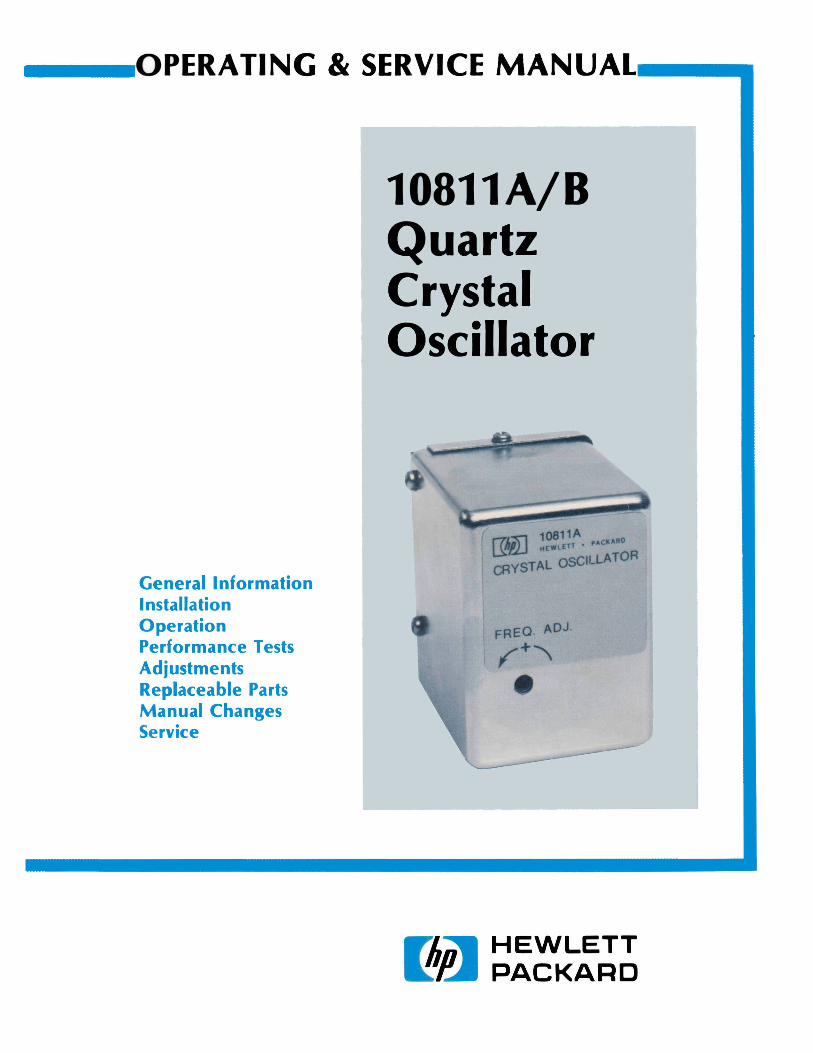
Figure 1-1. 10811A and 108118 Oscillators

Model 10811A/B
2
SECTION I
GENERAL INFORMATION
1-1. INTRODUCTION 1-2. This manual provides information pertaining to the installation, operation, testing, adjustment, and
maintenance of the HP Model 10811A/B Quartz Crystal Oscillator. Figure 1-1 shows the 10811A and 10811B.
1-3. This manual is divided into eight sections, each covering a particular topic. The topics by section number are shown below. Sections I, II, III appear in the Operating Instructions Manual. Sections I through VIII appear in the Operating and Service Manual.
Section Topic I General Information II Installation III Operation IV Performance Tests V Adjustments VI Replaceable Parts VII Manual Changes VIII Service
1-4. SPECIFICATIONS 1-5. Specifications are listed in Table 1-1. These specifications are the performance standards or
limits against which the oscillator may be tested.
1-6. SAFETY CONSIDERATIONS 1-7. The Model 10811A/B Component Oscillator is a Safety Class III product and must be powered
from a source which is electrically isolated from the mains (line circuits). Safety information pertinent to the operation and servicing of this instrument is included in the appropriate sections of this manual.
1-8. INSTRUMENTS COVERED BY THIS MANUAL 1-9. Attached to the instrument is a serial number plate. The serial number is in the form 0000A00000.
It is in two parts; the first four digits and the letter are the serial prefix and the last five are the suffix. The prefix is the same for all identical instruments; it changes only when a change is made to the instrument. The suffix, however, is assigned sequentially and is different for each instrument. The contents of this manual apply to instruments with the serial number prefix(es) listed under Serial Prefix on the title page.
1-10. An instrument manufactured after the printing of this manual may have a serial number prefix that is not listed on the title page. This unlisted serial number prefix indicates the instrument is different than those described in this manual. The manual for this new instrument is accompanied by a yellow Manual Changes supplement. This supplement contains "change information" that explains how to adapt the manual to the newer instrument.
1-11. In addition to change information, the supplement may contain information for correcting errors in the manual. To keep this manual as current and accurate as possible, Hewlett Packard recommends that you periodically request the latest Manual Changes supplement. The supplement for this manual is identified with the manual print date and part number, both of which appear on the manual title page. Complimentary copies of the supplement are available from Hewlett-Packard.

Model 10811A/B
3
Table 1-1. Specifications Table
Frequency Stability: (See Definition of Terms) Long Term (Aging Rate): <5 X 10⁻¹⁰/day after 24-hour warm-up. See Note 1. <1 X 10⁻⁷/year for continuous operation. Short Term: Refer to tables and figures above. Environmental Sensitivity: Temperature: <4.5 X 10⁻⁹ over a -55°C to 71°C range. <2.5 X 10⁻⁹ over a O°C to 71 °c range. Operating:-55°C to +71 °C. Storage: -55°C to X85°C. Load: <5 X 10⁻¹⁰ for a ±10% change in 50 ohm load. <5 X 10⁻¹⁰ for a ±25% change in 1KΩ load. Power Supplies: Oscillator Supply: <2 X 10⁻¹⁰ for 1% change. <100μv ripple and noise required. Oven Supply: <1 X 10⁻¹⁰ for 10% change. <30 mv ripple and noise required. Gravitational Field: <4 X 10⁻⁹ for 2g static shift (turn-over). Magnetic Field: <-90 dBc sidebands due to 0.1 millitesla (1 Gauss) rms at 100 Hz. Humidity (typical): 1 X 10⁻⁹ for 95% RH at 40°C. Shock (survival): 30g, 11ms, ½ sinewave. Altitude (typical): 2 X 10⁻⁹ for 0 to 50,000 ft. Warmup 10 min. after turn-on within 5 X 10⁻⁹ of final value, at 25°C and 20 Vdc. See Notes 1 & 2. Adjustment Coarse Frequency Range: >±1 X 10⁻⁶ (± 10 Hz) with 18 turn control. Elec. Frequency Control (EFC): ≥1 X 10⁻⁷
(1 Hz) total, control range -5 Vdc to +5 Vdc.
Output Frequency: 10 MHz Voltage: 0.55 ± 0.05 V rms into 50 ohm. 1V rms ±20%, into 1K ohm. Harmonic Distortion: Down more than 25 dB from output. Spurious Phase Modulation: Down more than 100 dB from output (discrete sidebands 10 Hz to 25 kHz). Power Requirements Oscillator Circuit: 11.0 to 13.5 Vdc. 30 mA typical. 40 mA max. Oven Circuit: 20 to 30 V dc; turn on load is 42 ohm minimum. Steady-state power drops to a typical value of 2.0W at 25°C in still air with 20 Vdc applied. Connectors 10811A: Mates with CINCH 50-30S-30 (HP 1251-0160) , Vishay/Dale (HP 1251-2035) EB81-BN15TGW, EDAC 305-030-500-202 or 357-030-520-202 or equivalent (not supplied). 10811B: Solder terminals and SMB Snap-on connectors. Mates with Cablewave Systems, Inc. #700156 or equivalent (not supplied). Accessories Available: Service Manual: HP 10811-90002: (not supplied). This Manual. Size: 72 mm X 52 mm X 62 mm, (see Figure 1). (2-13/16" X 2-1/32" X 2-7/16", 14 cu. in.).
Weight: 0.31 kg (11 oz.) Definition of Terms Long-Term Frequency Stability is defined as the absolute value (magnitude) of the fractional frequency change with time. An observation time sufficiently long to reduce the effects of random noise to an insignificant value is implied. Frequency changes due to environmental effects must be considered separately. Time Domain Stability σγ(τ) (Allan deviation) is defined as the two-sample deviation of fractional frequency fluctuations due to random noise in the oscillator. The measurement bandwidth is 100 kHz. Frequency Domain Stability is defined as the single sideband phase noise-to-signal ratio per Hertz of bandwidth (a power spectral density). This ratio is analogous to a spectrum analyzer display of the carrier versus either phase modulation sideband. See "NBS-Monograph 140" for measurement details. Notes: 1. For oscillator off-time less than 24
hours. 2. Final value is defined as frequency 24
hours after turn-on.
*Specifications describe the instrument's warranted performance. Supplemental characteristics are intended to provide information useful in applying the instrument by giving TYPICAL or NOMINAL, but non warranted performance parameters. Definition of terms is provided at the end of the specification section.

Model 10811A/B
4
1-12. For information concerning a serial prefix that is not listed on the title page or in the Manual Changes supplement, contact your nearest Hewlett-Packard office.
1-13. DESCRIPTION 1-14. The HP Model 10811A/B Quartz Crystal Oscillator is an extremely stable, compact, low power
source of 10 MHz. The 10811A/B has a very fast warm-up time, exhibits excellent temperature characteristics and has low phase noise and power consumption.
1-15. The 10811A/B has the ability to be adjusted over a range of 20 Hz (2 X 10⁻⁶), yet the control is sensitive enough to allow adjustment to better than 0.1 Hz (1 X 10⁻⁸). The frequency can also be controlled electronically over a 1 Hz (1 X 10⁻⁷) range with an externally applied voltage to the EFC.
1-16 The 10811A/B is field repairable, thus allowing the oscillator to be quickly placed back into service.
1-17. The 10811A/B requires two external power supplies. The power supply requirements are listed in Section II.
1-18. The 10811A and 10811B are identical, except for the connections. The 10811A uses a standard 15 pin printed circuit connector. The 10811B uses filtered-feedthrough terminals for power and oven monitor, and SMB subminiature rf snap-on connections for the 10 MHz output and EFC.
1-19. HP Part Number 10811-60101 and 10811-60105 1-20. The 10811-60101 is a 10811A in which phase noise, magnetic field and 2g turn-over are not
specified. The 10811-60101 is physically identical to the 10811A.
1-21. The 10811-60105 is a 10811-60101 with specifications of <1.5 X 10⁻⁹ for aging and <1 X 10-11 for short-term stability for a 1-second averaging time. The 10811-60105 is physically identical to the 10811A.
1-22. RECOMMENDED TEST EQUIPMENT 1-23. The test equipment required to maintain the Model 10811A/B is listed in Table 1-2. Other
equipment may be substituted if it meets or exceeds the critical specifications listed in the table.

Model 10811A/B
5
Table 1-2. Recommended Test Equipment
INSTRUMENT REQUIRED CHARACTERISTICS MODEL NO. 1. Frequency Analyzer* Phase noise measurement at 10 MHz 5390 5390A* cannot measure 10811 specs above 10 Hz 2. Frequency Counter** 10 MHz range, HP-IB programmable, 2 ns 5345A** resolution 3. Computing Controller** HP-IB compatible 9835A or 9825A ** 4. Frequency Reference Short term stability ≤5x10-12/second 5065A, 5061A Long term stability <5x10⁻¹⁰/day (Option 004), or 105A/B*** 5. Sampling Voltmeter ±3% accuracy at 10 MHz 3406A 6. General Purpose Bandwidth ≥ 10 MHz 1740A Oscilloscope 7. Frequency Doubler Operates at 10 MHz 10515A
8. Mixer Amplifier** 10 MHz Mixer/50 dB gain K79-59992A**
9. Spectrum Analyzer 10 MHz/70 dB range 8552B/8553B
10. Power Supply 480 mA @ 20V (2 required) 6215A 11. DC Voltmeter Any HP type digital or analog 12. Torque Screwdriver 2-30 inch-lb. (0.2 to 3.4 newton meters) 8730-0012 13. Feedthru Termination 50 ohms 11046B 14. BNC to Miniature Use for 10811B Only 05060-6116 Coax Adapter 15. Test Connector For testing 1 0811A See para. 8-61 *Not needed if items 2, 3, 4 are available. **Not needed if HP 5390A Frequency Stability Analyzer is available. ***If a 105A/B is used, its performance must be verified.
Model 10811A/B
6
SECTION II
INSTALLATION
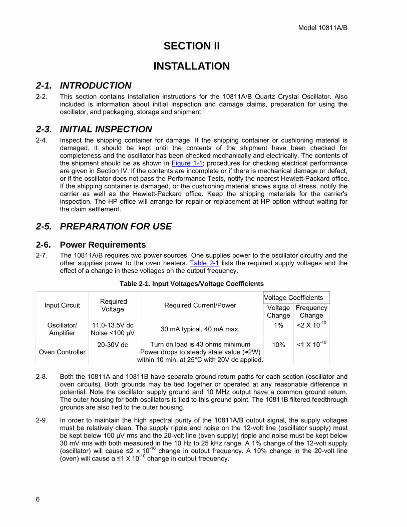
2-1. INTRODUCTION 2-2. This section contains installation instructions for the 10811A/B Quartz Crystal Oscillator. Also
included is information about initial inspection and damage claims, preparation for using the oscillator, and packaging, storage and shipment.
2-3. INITIAL INSPECTION 2-4. Inspect the shipping container for damage. If the shipping container or cushioning material is
damaged, it should be kept until the contents of the shipment have been checked for completeness and the oscillator has been checked mechanically and electrically. The contents of the shipment should be as shown in Figure 1-1; procedures for checking electrical performance are given in Section IV. If the contents are incomplete or if there is mechanical damage or defect, or if the oscillator does not pass the Performance Tests, notify the nearest Hewlett-Packard office. If the shipping container is damaged, or the cushioning material shows signs of stress, notify the carrier as well as the Hewlett-Packard office. Keep the shipping materials for the carrier's inspection. The HP office will arrange for repair or replacement at HP option without waiting for the claim settlement.
2-5. PREPARATION FOR USE
2-6. Power Requirements 2-7. The 10811A/B requires two power sources. One supplies power to the oscillator circuitry and the
other supplies power to the oven heaters. Table 2-1 lists the required supply voltages and the effect of a change in these voltages on the output frequency.
Table 2-1. Input Voltages/Voltage Coefficients
Voltage Coefficients Input Circuit Required
Voltage Required Current/Power Voltage Change
FrequencyChange
1% <2 X 10⁻¹⁰ Oscillator/ Amplifier
11.0-13.5V dc Noise <100 µV 30 mA typical, 40 mA max.
20-30V dc 10% <1 X 10⁻¹⁰
Oven Controller
Turn on load is 43 ohms minimum Power drops to steady state value (≈2W)
within 10 min. at 25°C with 20V dc applied.
2-8. Both the 10811A and 10811B have separate ground return paths for each section (oscillator and oven circuits). Both grounds may be tied together or operated at any reasonable difference in potential. Note the oscillator supply ground and 10 MHz output have a common ground return. The outer housing for both oscillators is tied to this ground point. The 10811B filtered feedthrough grounds are also tied to the outer housing.
2-9. In order to maintain the high spectral purity of the 10811A/B output signal, the supply voltages must be relatively clean. The supply ripple and noise on the 12-volt line (oscillator supply) must be kept below 100 µV rms and the 20-volt line (oven supply) ripple and noise must be kept below 30 mV rms with both measured in the 10 Hz to 25 kHz range. A 1% change of the 12-volt supply (oscillator) will cause ≤2 X 10⁻¹⁰ change in output frequency. A 10% change in the 20-volt line (oven) will cause a ≤1 X 10⁻¹⁰ change in output frequency.

Model 10811A/B
7
2-10. Single Source Regulated Power Supply 2-11. A single source of +20 to +30V dc with 10% regulation may be used to power both the oven and
oscillator amplifier circuits if a simple IC regulator is used. A suggested circuit is shown in Figure 2-1. The resistor and capacitor connected to terminals 3 and 4 of the IC minimize ripple and noise in the regulated output.
Figure 2-1. Single Source Regulated Power Supply
2-12. ELECTRONIC FREQUENCY CONTROL (EFC) 2-13. The EFC allows the oscillator to be tuned over a 1 Hz range (1 x 10⁻⁷) by applying -5 to +5 volts
to the EFC input. As the EFC voltage goes positive the output frequency will go lower. Conversely, as the EFC voltage goes negative, the output frequency will go higher.
2-14. Since noise on the EFC line affects the oscillator's stability (noise appears as FM on the output), care must be taken to ensure that a relatively noise free EFC voltage source is used. The noise level must be kept below 100 µV to maintain good stability performance.
2-15. The EFC input should be connected to oscillator circuit ground if not used. A shorting plug (1250-0911) is supplied with 10811B for this purpose. The EFC input on the 10811A should be grounded at the printed circuit connector by wiring pins 5 and 6 together.
2-16. 10 MHz FREQUENCY OUTPUT SIGNAL 2-17. The 10 MHz output is ac coupled from a source impedance of approximately 50 ohms. The signal
level is .55 ±.05 into a 50 ohms load or 1-volt ±20% into a 1 K ohm load.

Model 10811A/B
8
2-18. OVEN MONITOR OUTPUT 2-19. The OVEN MONITOR OUTPUT is an indicator of oven warm-up. At initial turn-on (warmup) the
oven monitor will go to approximately 1.5 volts BELOW the oven power supply voltage. After the oven cuts back, the output will drop to approximately 3.5 volts (at 25°C). The output impedance of this circuit is 10,000 ohms. Figure 2-2 shows an oven monitor LED indicator circuit.
Figure 2-2. Oven Monitor LED Circuit
2-20. MATING CONNECTORS AND MOUNTING 2-21. The 10811A Oscillator requires a 0.156” C-C 15-pin printed circuit connector. The recommended connector is the CINCH 250-15-30-210 50-30S-30 (HP 1251-0160), Vishay/Dale (HP 1251-2035) EB81-BN15TGW, EDAC 305-030-500-202 (Mouser 587-307-030) or 305-030-520-202. The 10811A can be secured with two 6-32 screws, 1/4-inch long. Figure 2-3 shows the power supply connection for the 10811A. Figure 2-5 shows the mechanical mounting dimension for the 10811A and 10811B.
Figure 2-3. 10811A Supply and Output Connections

Model 10811A/B
9
2-22. The 10811B Oscillator uses solder terminals with filtered feedthrough capacitors for power and oven monitor outputs and SMB subminiature rf snap-on connectors for the 10 MHz output and EFC. The 10811B also has one internally threaded mounting stud on the bottom cover and two located on the top. The three studs are threaded for 4-40 screws, 1/4-inch deep. These mounting studs may be used with vibration isolators such as the LORD #J2924-2-1 (HP Part No. 1520-0094). However, for ease of testing and interfacing, a 6-pin Amphenol connector is attached. If you wish to use this connector, the following parts are required to build its mate.
Part Number LORD J292421 Axial Load 1 (lbs) 4 (N) Deflection 0.006 (in) 1.5 (mm) Axial Spring Rate 17 (lbs/in) 2.6 (N/mm) Radial Spring Rate 17 (lbs/in) 2.6 (N/mm) Thickness 0.0625 (in) 1.6 (mm) Diameter 0.735 (in) 18.7 (mm)
Description Quantity HP Part No. Amphenol Part No.
Receptacle 1 1251-4297 221-1508 Pin-Female 5 1251-4734 220-883-03 Guide-Pin 2 1251-0597 221-590
2-23. If you do not wish to use the Amphenol connector, it may be easily removed. The SMB connectors mate to Cablewave Systems, Inc. #700156 or equivalent HP Part No. 1250-0885 (not supplied). Figure 2-4 shows the connections for the 10811B Oscillator.
Figure 2-4. 10811B Supply and Output Connections
2-23. INSTALLATION INSTRUCTIONS 2-24. Figure 2-5 shows the mechanical mounting dimensions of the 10811A/B Oscillators for use in
custom installation. Since all quartz oscillators are sensitive to shock, vibration, radiation fields, and ambient temperature changes, to obtain the best performance from your 10811A/B, these factors should be taken into consideration. To optimize performance therefore:
1. The 10811A/B should be mounted in an area that has a minimum amount of vibration or shock accelerations. In addition, the 10811A/B should be mounted so that the vibrational forces act along the "minimum G sensitivity" axis shown in Figure 2-5.
2. The 10811A/B should be mounted as far as possible from transformers or fan motors that radiate electromagnetic fields.
3. The 10811A/B should be mounted away from the main system airflow in order to isolate it as much as possible from ambient temperature changes.

Model 10811A/B
10
Figure 2-5. Mechanical Mounting Dimensions
2-25. INSTALLATION INSTRUCTIONS (HP INSTRUMENT) 2-26. The 10811A may be installed in most Hewlett-Packard instruments that already have a 10544A or
10544B oscillator or has provisions for it. The 10811A may be exchanged directly without any circuit change or modification.
2-27. If the instrument does not have a 10544A oscillator installed, but is available as an option, then the service manual for that instrument should be consulted to see if an oscillator support board (power supplies) is required. Once the support board is installed, the 10811A can be installed in place of the 10544A. Consult your nearest sales and service office for more details.
2-28. OPERATING ENVIRONMENT 2-29. TEMPERATURE. The 10811A/B may be operated in temperatures from -55°C to +71°C.
2-30. MAGNETIC FIELDS. Sidebands due to 0.1 milliTelsa (1 Gauss) rms at 100 Hz will be down more than 90 dB from carrier.
2-32. ALTITUDE. The frequency change will be typically 2 X 10⁻⁹ for altitudes up to 15.2 km (50,000 ft.).
2-33. SHOCK. The 10811A/B can withstand a shock up to 30 Gs for 11 ms, 1/2 sine wave.

Model 10811A/B
11
2-34. STORAGE AND SHIPMENT
2-35. Environment 2-36. The 10811A/B may be stored or shipped in environments with the following limits: Temperature ····························· -55°C to +85°C Altitude ······································ 15.2 Km (50,000 feet)
2-37. PACKAGING
2-38. Original Packaging 2-39. Containers and materials identical to those used in factory packaging are available through
Hewlett-Packard offices. If the instrument is being returned to Hewlett-Packard for servicing, attach a tag indicating the type of service required; return address, model number, and full serial number. Also, mark the container Fragile to ensure careful handling. In any correspondence, refer to the instrument by model number and full serial number.
2-40. Other Packaging 2-41. The following general instructions should be used for repacking with commercially available
materials.
1. Wrap instrument in heavy paper or plastic. (If shipping to Hewlett-Packard office or service center, attach tag indicating type of service required; return address, model number, and full serial number.)
2. Use strong shipping container. A double-wall carton made of 350-pound test material is adequate.
3. Use a layer of shock-absorbing material 70 to 100 mm (3 to 4 inch) thick around all sides of the instrument to provide firm cushioning and prevent movement inside container. Protect control panel with cardboard.
4. Seal shipping container securely.
5. Mark shipping container FRAGILE to insure careful handling.
6. In any correspondence, refer to instrument by model number and full serial number.

Model 10811A/B
12
SECTION III
OPERATION
3-1. INTRODUCTION 3-2. This section contains operating information including operating characteristics and operating
procedure.
3-3. BASIC POWER-UP DESCRIPTION 3-4. The following paragraph is a basic description of the actions occurring when power is applied to
the oscillator. This description assumes the oscillator is at room temperature (25°C).
3-5. When power is applied to the oscillator, 10 MHz will appear at the output. The oven controller circuit will go into its full warm-up mode. In this mode the maximum heating power is applied to the oven mass. The oven mass is a metal casting surrounding the oscillator circuits and crystal. The OVEN MONITOR output will be approximately 1.5 volts below the oven power supply voltage. In about 10 minutes, the oven will have heated to the proper temperature. The oven controller will begin to regulate at this temperature, and the OVEN MONITOR will drop to approximately 3.5 volts. It is normal for the oven current to drop momentarily to a low value when the oven temperature first reaches maximum. This lasts less than second and is a typical circuit action.
3-6. After the first 10 minutes have passed, the oscillator may be initially adjusted using the following procedure. The oscillator should be readjusted after 24 hours for maximum accuracy. Periodic adjustment schedule can be determined by the procedure described in paragraph 3-10.
3-7. FREQUENCY ADJUSTMENT 3-8. The frequency adjustment is the only periodic adjustment required. This may be initially adjusted
after 10 minutes of warm-up and then readjusted after 24 hours.
3-9. FREQUENCY ADJUSTMENT PROCEDURE a. Connect reference frequency standard (multiple or submultiple of 10 MHz) to the EXTERNAL
SYNC INPUT of the oscilloscope.
b. Connect oscillator output (10811A/B) to Channel A. Set the sweep speed to .1 μs/div.
c. Set the oscilloscope to EXTERNAL TRIGGER and adjust the oscilloscope so that its sweep is synchronized to the reference frequency. The pattern will appear to move.
d. Using an insulated tuning tool, adjust oscillator frequency adjustment (FREQ ADJUST on the 10811A/B) for minimum sideways movement of the oscilloscope pattern.
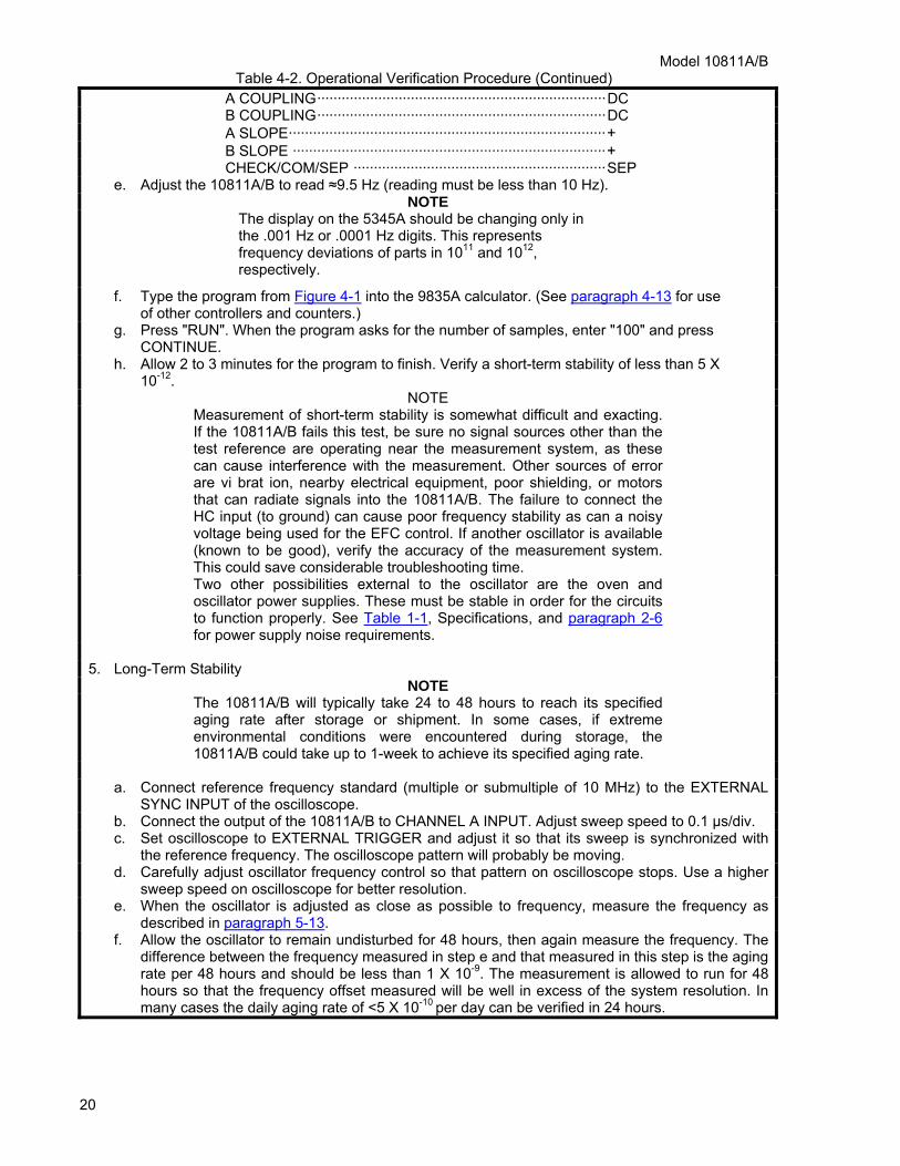
e. By timing the sideways movement (divisions per second on the oscilloscope), the approximate offset can be determined based on the oscilloscope sweep speed shown in Figure 3-1

Model 10811A/B
13
f. For example, if the trace moves 1 division in 10 seconds and the sweep speed is 0.01 μs/div., the oscillator's frequency is 1 x 10⁻⁹ different from that of the reference frequency, as can be seen from the calibration, Table 3-1. The calculation can also be made by the following formula:
where Δf/f = offset of the oscillator with respect to the reference standard Δt = the movement of the oscilloscope pattern (1 div. X .01 μs/div.) = .01, μs t = time required for Δt to occur.
Figure 3-1. Oscillator Adjustment Set-Up
3-10. ACCURACY VS ADJUSTMENT INTERVAL 3-11. Table 3-1 shows the required adjustment interval to maintain a required accuracy. If the aging
rate is known to be 3 x 10⁻¹⁰/day, then a more precise adjustment interval can be determined. (The specification for aging is <5 X10⁻¹⁰/day, but aging is typically less than this.) The aging rate can be expected to gradually decrease, and typically will reach 1 X 10⁻¹⁰/day within 1-year.
Example:
Known aging rate···········································3 X 10⁻¹⁰/day Maximum allowable error ·····························5 X 10⁻⁹

Model 10811A/B
14
3-12. Find the line on Table 3-1 corresponding to the oscillator's aging rate. Then find the maximum allowable error (accuracy) on the horizontal axis. Follow the maximum allowable error vertically until it crosses the oscillator's known aging rate. Move horizontally to the left and read the minimum calibration interval in days.
maximum allowable error known aging rate (per day) = calibration interval in days
Example:
5 x 10⁻⁹ (maximum allowable error) 3 x 10⁻¹⁰/day (known aging rate) = 16.67 days (~17 days) 3 X 10⁻¹⁰/day (known aging rate)
3-13. From Table 3-1, the oscillator should be adjusted approximately every 17 days.
3-14. The minimum calibration interval may also be determined from the following formula:
Table 3-1. Accuracy vs Adjustment

Model 10811A/B
15
Page Intentionally Left Blank
Model 10811A/B
16
SECTION IV
OPERATIONAL VERIFICATION
4-1. INTRODUCTION 4-2. The tables in this section test the instrument's performance using the specifications of Table 1-1
as the performance standards. All tests can be performed without access to the interior of the instrument.
4-3. OPERATIONAL VERIFICATION 4-4. The Operational Verification, Table 4-2, can be performed to give a high degree of confidence
that the 10811A/B is operating properly without performing the complete performance tests. The operational verification should be useful for incoming QA, routine maintenance, and after instrument repair.
4-5. EQUIPMENT REQUIRED 4-6. Equipment required for the operational verification is listed in the recommended test equipment in
Section I, Table 1-2, and in Table 4-1. Any equipment that satisfies the critical specifications given in the table may be substituted for the recommended model(s).
4-7. TEST RECORD 4-8. Results of the Operational Verification, Table 4-2, may be tabulated on the Operational
Verification Record, Table 4-4.
4-9. If the 10811A/B Oscillator is to be tested outside its normal installation, a special test connector may be used for applying power to the oscillator. The connector also has a BNC connector for the 10 MHz output signal. A photo, parts list, and construction information is located in Section VIII. The connector should be used under the following circumstances:
a. If the 10 MHz output is not easily accessible.
b. If there is a buffer amplifier between the 10811A/B output and the oscillator output jack on the rear panel of the instrument.
c. Troubleshooting.
d. If testing of the oscillator in its normal installation causes erroneous measurements (e.g., fan noise, vibrations, noisy circuits, etc.). If in doubt, use the special test connector.
4-10. Table 4-1 lists the five sections of the operational verification and their descriptions.
Model 10811A/B
17
Table 4-1. Operational Verification Descriptions
1. Amplitude (0.55 volts (±0.05 volts/50Ω, 1 volt ± 0.2 volt/1kΩ). a. Equipment required:
BNC-to-BNC Cable 500 and 1 KΩ loads 3406A AC Voltmeter
2. Harmonic Distortion (-25 dB below 10 MHz output signal). a. Equipment required:
141T Display Section 8553B Spectrum Analyzer - RF Section 8552B Spectrum Analyzer - IF Section BNC-to-BNC Cable
3. Spurious Signals - Signals unrelated to the 10 MHz output signal (-100 dB below the 10 MHz output signal).
NOTE Due to the complexity of measuring signal 100 dB below a reference, this procedure will verify that no spurious signals exist greater than 65 dB below the normal 10 MHz output signal.
4. a. Equipment required:
141T Display Section 8553B Spectrum Analyzer - RF Section 8552B Spectrum Analyzer - IF Section BNC-to-BNC Cable
5. Short Term Stability (5 X 10-12 for 1-second averaging; 1 X 10-11 for 10811-60105). a. Equipment required:
5065A Rubidium Vapor Frequency Standard 5061A Option 004, or 105A/B, See Table 1-2 HP Model 5390A may be used in place of the following:
10830A Mixer 5345A Electronic Frequency Counter with Option 011 9825A Calculator with 98210A and 98213A or 98214A or 98216A 98034A HP-IB Interface
10515A Doubler 6-Plug AC Power Strip 3 BNC-to-BNC Cables
6. Long Term Stability -<5 X 10⁻¹⁰ over 24 hours; 1.5 X 10⁻⁹/24 hours for 10811-60105. a. Equipment required:
HP 1740A 100 MHz Oscilloscope, 105A/B Quartz Crystal Oscillator, 5065A Rubidium Frequency Standard, or 5061A Cesium Beam Frequency Standard. See Table 1-2.
4-11. In the following tests, the power supply voltages to the oscillator are not shown. They are
assumed to be:
Oscillator Circuits ........................................ +12V dc Oven Circuits ............................................... +20V dc 4-12. Any supply voltages within the specified limits listed in Table 1-1 may be used and will not affect
the operational verification. The voltages are only reference points and are used throughout this manual.

Model 10811A/B
18
Table 4-2. Operation Verification Procedure
1. Amplitude Test
Procedure: a. Set the 3406A Voltmeter to the l-volt range. b. Insert the 3406A Voltmeter probe into the 1 volt jack on the front panel. c. With the CAL button out, set the 3406A to zero by adjusting the ZERO control on the front
panel. d. Press the CAL button and adjust the 3406A to read 1V by adjusting the CALIBRATE control
on the front panel. e. Remove the probe from the 1-volt jack and conned to the 10811A/B output through a 50 ohm
termination. f. Verify amplitude of 0.55 volts ±0.05 volts. Mark the test card. g. Remove the 50Ω termination and replace with a 1 kΩ termination. h. Verify amplitude of 1 volt ±0.2 volt.
2. Harmonic Distortion
a. Set 141T Spectrum Analyzer controls to: TUNING STABILIZER··········································OFF BANDWIDTH ······················································ 30 kHz SCAN WIDTH per Division ································· 5 MHz/div. INPUT ATTENUATION ······································· 50 dB VIDEO FILTER ····················································OFF SCAN TIME ························································· 10 ms/div. SCAN MODE ······················································ INT SCAN TRIGGER ·················································AUTO LOG REF LEVEL ················································ +10 LOG/LINEAR Switch············································ 10 dB LOG
b. Connect the output of the 10811A/B to the spectrum analyzer input. c. Apply power to the oscillator and spectrum analyzer. Allow 10 minutes for oscillator to
stabilize. d. Adjust Spectrum Analyzer FREQUENCY control so that 10 MHz signal is at left-edge of
display (center frequency, approximately 35 MHz). e. Adjust LOG REF LEVEL vernier control (right hand knob) so that 10 MHz signal is at top of
display gratitude. Verify that all harmonics of the 10 MHz signal are more than 25 dB down. Leave spectrum analyzer connected for next test.
3. Spurious Output Signals
a. Use the test setup as described in Test 2. b. Set the Spectrum Analyzer controls to:
TUNING STABILIZER··········································OFF BANDWIDTH ······················································· 1 kHz SCAN WIDTH ······················································ .05 MHz INPUT ATTN························································ 50 dB LOG REFERENCE ··············································+10 dBm SCAN TIME··························································0.1 s/div. VIDEO FILTER ···················································· 100 Hz SCAN MODE ······················································ INT SCAN TRIGGER ·················································AUTO FREQUENCY······················································· 10 MHz (0-11 MHz RANGE)
c. Adjust FREQUENCY so 10 MHz signal is at center of display. Adjust LOG REF LEVEL so
signal is at top of graticule. d. Set TUNING STABILIZER switch "on" (up) and reset Spectrum Analyzer controls as follows:
BANDWIDTH ······················································· .03 kHz (30 Hz) SCAN WIDTH ······················································ 5 kHz SCAN TIME··························································10 s/div.

Model 10811A/B
19
Table 4-2. Operational Verification Procedure (Continued)
e. Set INTENSITY and PERSISTENCE controls for an easily readable display at the 10 s scan time.
f. Verify that there are no repeating signals above a level 65 dB below the 10 MHz signal (i.e., no signals between -64 dB and 0 dB). Allow the analyzer to sweep through several times to verify that no signals repeat on successive sweeps. Signals greater than -65 dB indicate possible spurious signals on 10811A/B output. Be sure there is no other equipment nearby that could be radiating signals into the measurement. Be sure power supplies meet noise specifications as described in Table 1-1.
4. Short-Term Stability NOTE
If the model 5390A frequency stability analyzer is available it should be used in place of the text described below. Follow instructions in the 5390A operating manual to make measurement.
a. Connect the equipment as follows:
NOTE
Arrange the instruments as shown. Keep all signal leads away from power cords and HP-IB cable. DO NOT FORGET THE 10515A DOUBLER ON THE 5065A OUTPUT. Connect all ac power to the same strip so that all ground paths are as short as possible. DO NOT STACK THE INSTRUMENTS. Use coax for all signal leads.
b. Set the 5345A address to 18:
A5 A4 A3 A2 1 (16) 0 (8) 0 (4) 1 (2) = 18
c. Allow 1-hour warmup to stabilize the test equipment and the 10811A/B. d. Set the 5345A front panel controls as follows:
FUNCTION ·········································································· FREQ A GATE TIME ········································································· 1 s SAMPLE RATE ··································································· max (ccw) GATE CONTROL INPUT (REAR PANEL) ·························· INTERNAL A LEVEL ·············································································· PRESET B LEVEL ·············································································· PRESET A IMPEDANCE ··································································· 50 ohm B IMPEDANCE ··································································· 50 ohm A ATTENUATOR ································································ X1 B A TTENUATOR ······························································· X1
Model 10811A/B
20
Table 4-2. Operational Verification Procedure (Continued) A COUPLING·······································································DC B COUPLING·······································································DC A SLOPE··············································································+ B SLOPE ·············································································+ CHECK/COM/SEP ······························································SEP
e. Adjust the 10811A/B to read ≈9.5 Hz (reading must be less than 10 Hz). NOTE
The display on the 5345A should be changing only in the .001 Hz or .0001 Hz digits. This represents frequency deviations of parts in 1011 and 1012, respectively.
f. Type the program from Figure 4-1 into the 9835A calculator. (See paragraph 4-13 for use of other controllers and counters.)
g. Press "RUN". When the program asks for the number of samples, enter "100" and press CONTINUE.
h. Allow 2 to 3 minutes for the program to finish. Verify a short-term stability of less than 5 X 10-12.
NOTE Measurement of short-term stability is somewhat difficult and exacting. If the 10811A/B fails this test, be sure no signal sources other than the test reference are operating near the measurement system, as these can cause interference with the measurement. Other sources of error are vi brat ion, nearby electrical equipment, poor shielding, or motors that can radiate signals into the 10811A/B. The failure to connect the HC input (to ground) can cause poor frequency stability as can a noisy voltage being used for the EFC control. If another oscillator is available (known to be good), verify the accuracy of the measurement system. This could save considerable troubleshooting time. Two other possibilities external to the oscillator are the oven and oscillator power supplies. These must be stable in order for the circuits to function properly. See Table 1-1, Specifications, and paragraph 2-6 for power supply noise requirements.
5. Long-Term Stability
NOTE The 10811A/B will typically take 24 to 48 hours to reach its specified aging rate after storage or shipment. In some cases, if extreme environmental conditions were encountered during storage, the 10811A/B could take up to 1-week to achieve its specified aging rate.
a. Connect reference frequency standard (multiple or submultiple of 10 MHz) to the EXTERNAL
SYNC INPUT of the oscilloscope. b. Connect the output of the 10811A/B to CHANNEL A INPUT. Adjust sweep speed to 0.1 μs/div. c. Set oscilloscope to EXTERNAL TRIGGER and adjust it so that its sweep is synchronized with
the reference frequency. The oscilloscope pattern will probably be moving. d. Carefully adjust oscillator frequency control so that pattern on oscilloscope stops. Use a higher
sweep speed on oscilloscope for better resolution. e. When the oscillator is adjusted as close as possible to frequency, measure the frequency as
described in paragraph 5-13. f. Allow the oscillator to remain undisturbed for 48 hours, then again measure the frequency. The
difference between the frequency measured in step e and that measured in this step is the aging rate per 48 hours and should be less than 1 X 10⁻⁹. The measurement is allowed to run for 48 hours so that the frequency offset measured will be well in excess of the system resolution. In many cases the daily aging rate of <5 X 10⁻¹⁰ per day can be verified in 24 hours.

Model 10811A/B
21
Figure 4-1. BASIC Program
4-13. OPTIONAL CONTROLLERS AND COUNTERS
4-14. Optional Controllers 4-15. Figure 4-2 lists the program for the 9825A Calculator.
Figure 4-2. HPL Program
10 ! Short term stability test 10811A/B 20 INPUT “Enter number of samples”,Samples 30 Loop = 0 40 OUTPUT 7,18; “I2E1<:8I2” !5325A Codes 50 ENTER 7,18;A !Empty dummy buffer 60 ENTER 7,18;A !First measurement 70 Count = 0 80 FOR Loop = 1 to Samples 90 ENTER 7,18; B !Successive measurements 100 Count = Count + (A-B)^2 110 A=B 120 FIXED 0 130 DISP Loop 140 NEXT Loop 150 PRINTER IS 0 160 FLOAT 1 170 PRINT “STS=”;SQR(Count/(2*Loop))/1E7 180 GOTO 50 190 STOP
0: 1: “Short term stability test 10811A/B” 2: “100 Samples is standard value” : ent “Enter number of samples”,S 3: 0→L 4: “5345A Codes” : wrt 718,”I2E1<:8I2” 5: “Empty dummy buffer” : red 718,A 6: “First measurement” : red 718,A 7: 0→C 8: for L=1 to S 9: “Successive measurements” : red 718,B 10: C+(A-B)^2→C 11: B→A 12: fxd 0 13: dsp L 14: next L 15: 16: flt 1 17: “Short term stability formual”: prt “STS=”,SQR(C/(2*L))/1e7 18: gto 5 19: stp

Model 10811A/B
22
4-16. Optional Counters 4-17. Table 4-3 shows the program codes set required when using the 5316A counter. Replace line 4
(HPL) or line 40 (BASIC) with the appropriate codes. Be sure the optional counter address is set to "18".
5316A (gate time must be set manually to 1 s on the front panel)
Table 4-3. 5316A Program Codes

Model 10811A/B
23
Page Intentionally Left Blank

Model 10811A/B
24
Table 4-4. Operational Verification Record

Model 10811A/B
25
SECTION V
ADJUSTMENTS
5-1. INTRODUCTION 5-2. This section describes the adjustments required to maintain the 10811A/B operating characteristics within specifications. Adjustments should be made when required, such as after a performance test failure or when components are replaced that may affect an adjustment.
5-3. EQUIPMENT REQUIRED 5-4. The test equipment required for the adjustment procedure is listed in Table 1-2, Recommended Test Equipment. Substitute instruments may be used if they meet the critical specifications.
5-5. FACTORY SELECTED COMPONENTS 5-6. Some of the values in the parts lists are selected during manufacturing to meet circuit requirements. These parts are marked with an asterisk (*) in the parts list and schematic diagrams, with average value shown.
5-7. ADJUSTMENT LOCATION 5-8. Adjustment locations are identified in this section and in the component locators in Section VIII, Schematic Diagrams.
5-9. SAFETY CONSIDERATIONS 5-10. This section contains warnings and cautions that must be followed for your protection and to avoid damage to the equipment.
WARNING MAINTENANCE DESCRIBED HEREIN IS PERFORMED WITH POWER SUPPLIED TO THE INSTRUMENT, AND PROTECTIVE COVERS REMOVED. SUCH MAINTENANCE SHOULD BE PERFORMED ONLY BY SERVICE-TRAINED PERSONNEL WHO ARE AWARE OF THE HAZARDS INVOLVED (FOR EXAMPLE, FIRE AND ELECTRICAL SHOCK). WHERE MAINTENANCE CAN BE PERFORMED WITHOUT POWER APPLIED, THE POWER SHOULD BE REMOVED. BEFORE ANY REPAIR IS COMPLETED, ENSURE THAT ALL SAFETY FEATURES ARE INTACT AND FUNCTIONING, AND THAT ALL NECESSARY PARTS ARE CONNECTED TO THEIR PROTECTIVE GROUNDING MEANS.
5-11. OSCILLATOR FREQUENCY ADJUSTMENT 5-12. The following frequency adjustment procedure is the same for both the 10811A and 10811B.
Allow the oscillator to warm up for 24 hours before making this adjustment. See Figure 5-1.
a. Connect reference frequency standard (multiple or submultiple of 10 MHz) to the EXTERNAL SYNC INPUT of the oscilloscope. Adjust oscilloscope so that sweep is synchronized with reference frequency.
Model 10811A/B
26
Figure 5-1. Oscillator Adjustment Setup
b. Connect oscillator output to Channel A of the oscilloscope. Adjust sweep speed so pattern movement can be seen.
c. Adjust oscillator frequency adjustment (FREQ AD) on 10811A/B Crystal Oscillator unit) for minimum sideways movement of the 10 MHz displayed signal. Increase oscilloscope sweep speed for greater resolution.
5-13. Offset Calculation: a. By timing the sideways movement (divisions per second on the oscilloscope), the approximate offset
can be determined based on the oscilloscope sweep speed as shown below.
b. For example, if the trace moves 5 divisions in 10 seconds and the sweep speed is 0.01 μs/div., the oscillators signal is within 5 X 10⁻⁹ of the reference frequency. The calculation can also be made as follows:
Where:
Δf/f is the normalized frequency difference between the 10811A/B and the reference signal Δt is the change observed in the oscilloscope t is the time required for Δt to occur.

Model 10811A/B
27
5-14. OUTPUT AMPLITUDE ADJUSTMENT 5-15. The output amplitude is adjusted by the setting of the variable resistor R6 which is in the feedback of the AGC circuitry. It is not accessible from the outside of the oscillator. 5-16. The following procedure should be used to adjust the output amplitude only if the output level falls outside the specified level, or repairs have been made to the main oscillator or AGC circuitry.
1. Remove oscillator from instrument.
WARNING THE OSCILLATOR'S INTERNAL OVEN MASS TEMPERATURE MAY BE AS HIGH AS 85°C (185°F). TO AVOID SERIOUS BURNS DO NOT REMOVE OSCILLATOR CIRCUITS AND/OR OVEN MASS ASSEMBLY FROM THE OUTER HOUSING UNTIL THE OSCILLATOR HAS SUFFICIENTLY COOLED (APPROXIMATELY 1 HOUR WITH BOTTOM COVER AND FOAM INSULATOR REMOVED). THE OUTER HOUSING TEMPERATURE IS NOT A RELIABLE INDICATION OF THE INTERNAL TEMPERATURE.
2. Remove bottom cover and allow oscillator to cool (if previously operated). To remove cover:
a. For the 10811A, remove the three screws securing the bottom cover. Remove the two screws
securing the P.c. edge connector to the outer can. Remove the top foam insulator to expose the oscillator circuits.
CAUTION
DO NOT pull the oscillator out of the outer housing by pulling on the P.C. edge connector or flex circuit!!
b. For the 10811B remove the four screws securing the bottom cover. Disconnect the bottom cover flex circuit from the seven pin connector.
3. Once the oscillator is cool enough to
handle, remove the oscillator assembly by pushing on the tuning capacitor (top of oscillator) with a long, small diameter tool until the oscillator assembly can be removed freely.
NOTE
Under no circumstances should the oven circuit be operated with the oven mass removed from the outer housing. To do so will cause damage to components inside the oven mass.
4. Obtain HP Model 6215A Power Supply or equivalent. Preset power supply to 12V dc. Turn off power supply before proceeding to next step.
Figure 5-2. 10811A Amplitude Adjustment Set-up

Model 10811A/B
28
5. For the 10811A, connect Model 6215A Power Supply to pins 2 Hand 3 (+) of a 15 pin printed circuit connector.
a. Insert the 10811A P.c. edge connector
into the 15 pin P.c. connector. (See Section VIII for a special 10811A test connector.)
b. Connect pin 1 of the 15 pin pc connector
through a 50Ω termination (use pin 2 as ground) to a 3406A Sampling Voltmeter. See Figure 5-2. Do not apply power to the oven circuits.
c. For the 10811B, reconnect the flex
circuit attached to the bottom cover and connect the 6215A as shown in Figure 5-3. DO NOT APPLY POWER TO THE OVEN CIRCUITS. A Micon to BNC adaptor is available for the 10 MHz output (HP Part Number 05060-6116).
d. For both 10811A and B, turn on the
6215A power supply and adjust R6 AGC control for .55V rms ±50 mV as read on the 3406A Sampling Voltmeter. R6 is accessible through the small hole in the side of the oven mass.
6. Turn off the 6215A power supply and
reassemble the oscillator.
Figure 5-3. 108118 Amplitude Adj Set-up

Model 10811A/B
29
SECTION VI
REPLACEABLE PARTS
6-1. INTRODUCTION 6-2. This section contains information for ordering replacement parts. Table 6-1 lists parts in
alphanumerical order of their reference designators and indicates the description and HP Part Number of each part, together with any applicable notes. The table includes the following information.
a. Description of part (see abbreviations below). b. Typical manufacturer of the part in a five-digit code; see list of manufacturers in Table 6-2. c. Manufacturer's part number. d. Total quantity used in the instrument (Qty column).
6-3. ORDERING INFORMATION 6-4. To obtain replacement parts, address order of inquiry to your local Hewlett-Packard Sales and
Service Office (see lists at rear of this manual for addresses). Identify parts by their Hewlett Packard part numbers.
a. Instrument model number. b. Instrument serial number. c. Description of the part. d. Function and location of the part. e. Check digit. f. Quantity required.
6-5. HP PART NUMBER ORGANIZATION 6-6. The following is a general description of the HP part number system.
Model 10811A/B
30
6-7. Component Parts and Materials 6-8. Generally, the prefix of HP part numbers identifies the type of device. Eight-digit part numbers are used, where the four-digit prefix identifies the type of component, part, or material and the four-digit suffix indicates the specific type. Following is a list of some of the more commonly used prefixes for component parts. The list includes HP manufactured parts and purchased parts.
Prefix Component Part Material 0121- Capacitors, Variable (mechanical) 0122- Capacitors, Voltage Variable (semiconductor) 0140- Capacitors, Fixed 0150- Capacitors, Fixed, 0160- Capacitors, Fixed 0180- Capacitors, Fixed Electrolytic 0330- Insulating Materials0340- Insulators, Formed 0370- Knobs, Control 0380- Crystals 0470- Adhesives0490- Relays 0510- Fasteners
0674- through 0778- Resistors, Fixed (non wire wound) 0811- through 0831- Resistors (wire wound)
1200- Sockets for components 1205- Heat Sinks1250- Connectors (RF and related parts) 1251- Connectors (non RF and related parts) 1410- Bearings and Bushings 1420- Batteries 1820- Monolithic Digital Integrated Circuits 1826- Monolithic Linear Integrated Circuits 1850- Transistors, Germanium PNP 1851- Transistors, Germanium NPN 1853- Transistors, Silicon PNP 1854- Transistors, Silicon NPN 1855- Field-Effect- Transistors
1900- through 1912- Diodes 1920- through 1952- Vacuum Tubes
1990- Semiconductor Photosensitive and Light-emitting Diodes 3100- through 3106- Switches
8120- Cables 9100- Transformers, Coils, Chokes, Inductors, and Filters
6-9. For example, 1854-0037, 1854-0221 and 1851-0192 are all NPN transistors. The first two are silicon and the last is germanium.

Model 10811A/B
31
6-10. GENERAL USAGE PARTS 6-11. The following list gives the prefixes for HP manufactured parts used in several instruments, e.g.,
side frames, feet, top and bottom covers, etc. These are eight-digit part numbers with the four-digit prefix identifying the type of parts as shown below:
Type of Part P/N Suffix Sheet Metal 5000- to 5019- Machined 5020- to 5039- Molded 5040- to 5059- Assembly 5060- to 5079 Component 5080- to 5099
6-12. Specific Instrument Parts 6-13. These are HP manufactured parts for use in individual instruments or series of instruments. For
these parts, the prefix indicates the instrument and the suffix indicates the type of part. For example, 05328-60001 is an assembly used in the 5328A. Following is a list of suffixes commonly used.
Type of Part P/N Suffix Sheet Metal -00000 to -00499Machined -20000 to -20499Molded -40000 to -40499Assembly -60000 to -60499Component -80000 to -80299Documentation -90000 to -90249
6-14. Factory Selected Parts 6-15. Some of the values in the parts list are selected during manufacture to meet circuit requirements.
These parts are marked with an asterisk (*) in the parts list and schematic diagrams, with average values shown.
6-16. The 10811A/B Oscillator contains only one factory selected part which is R20 OVEN TEMPERATURE SET resistor. This resistor is supplied with the crystal, should the crystal require replacement. Table 8-1 lists the various resistors and their corresponding part numbers.
6-20. REPLACEABLE PARTS LIST LAYOUT 6-21. The 10811A and 10811B Oscillators are identical internally, except that the 10811B has had the
15-pin pc edge connector removed and a 7-pin connector (11) placed on the board for the 10811B bottom cover flex circuit (see Figure 8-15). The only other difference is the outer housings. Thus the parts lists for the circuit boards are identical. The parts lists are set up in the following manner:
1. 10811A and 10811B Circuit Board Components and Miscellaneous Parts. 2. 10811A and 10811B Transistor Mounting Hardware. 3. 10811A and 10811B Oven Mass Assembly and covers. 4. 10811A Mechanical Parts (Housing). 5. 10811B Mechanical Parts (Housing).

Model 10811A/B
32
Table 6-1. Replaceable Parts
Reference Designation
HP Part Number
C D
Qty Description Mfr Code
Mfr Part Number
10811-60001 3 1 CIRCUIT BOARD COMPONENTS 10811A/B 28480 10811-60001 C1 0121-0511 6 1 TUNING CAPACITOR 28480 0121-0511 C2 0160-0576 5 11 CAPACITOR-FXD .1uF ±20% 50VDC CER 28480 0160-0576 C3 0160-5109 0 1 CAPACITOR-FXD 15pF ±5% 50VDC CER 0±30 28480 0160-5109 C4 0160-0576 5 CAPACITOR-FXD .1uF ±20% 50VDC CER 28480 0160-0576 C5 0160-0576 5 CAPACITOR-FXD .1uF ±20% 50VDC CER 28480 0160-0576 C6 0160-4935 8 CAPACITOR-FXD 510pF ±1% 100VDC CER 72982 8121-100-COGO-511F C7 0160-0576 5 CAPACITOR-FXD .1uF ±20% 50VDC CER 28480 0160-0576 C8 0160-5110 3 1 CAPACITOR-FXD 62pF ±1% 50VDC CER 0±30 28480 0160-5110 C9 0160-0576 5 CAPACITOR-FXD .1uF ±20% 50VDC CER 28480 0160-0576 C10 0160-3874 2 2 CAPACITOR-FXD 10pF ±.5PF 200VDC CER 28480 0160-3874 C11 0160-0576 S CAPACITOR-FXD .1uF ±20% 50VDC CER 28480 0160.0576 Cl2 0160-4512 7 2 CAPACITOR-FXD 120pF ±5% 200VDC CER 51642 200-200-NP0-121J C13 0160-3479 7 3 CAPACITOR-FXD .01uF ±20% 100VDC CER 28480 0160-3879 C14 0160-0576 5 CAPACITOR-FXD .1uF ±20% 50VDC CER 28480 0160-0576 C15 0180-2617 1 1 CAPACITOR-FXD 6.8uF +.10% 35VDC TA 25085 D6R8G81B35K C16 0160-0576 5 CAPACITOR-FXD .1uF ±20% 50VDC CER 28480 0160-0576 C17 0160-3874 2 CAPACITOR-FXD 10pF ±.5pF 200VDC CER 28480 0160-3874 C18 0160-4947 2 1 28480 0160-4947 C19 0160-3879 7 CAPACITOR-FXD .01uF ±20% 100VDC CER 28480 0160-3879 C20 0160-3879 7 CAPACITOR-FXD .01uF +.20% 100VDC CER 28480 0160-3879 C21 0160-0576 5 CAPACITOR-FXD .1uF +.20% 50VDC CER 28480 0160-0576 C22 0160-0576 5 CAPACITOR-FXD .1uF +.201 50VDC CER 28480 0160-0576 C23 0160-4512 7 CAPACITOR-FXD 120pF +.5% 200VDC CER 51642 200-200-NP0-121J C24 0160-0576 5 CAPACITOR-FXD .1uF +.20% 50VDC CER 28480 0160-0576 CR1 0122-0244 4 1 DIODE-VVC 100PF 5% C4/C25-MIN=2 BVR-30V 28480 0122-0244 CR2 1901-0869 2 1 DIODE-CUR RGLTR 1N5297 DO=7 04713 1N5297
CR3 1902-0984 4 1 DIODE-ZNR 6,4V 2% DO=7 PD = .4W TC=+.002%
28480 1902.0984
CR4 1901-0535 9 3 DIODE-SCHOTTKY 28480 1901.0535 CR5 1901-053S 9 DIODE-SCHOTTKY 28480 190100535 CR6 1901-0535 9 DIODE-SCHOTTKY 28480 1901-0535 E1 9170-0029 1 FERRITE BEAD (FOR Q1) 28480 9170-0029 F1 2110-0617 6 1 FUSE-THERMAL (10811-80008) 28480 2110-0617 L1 9100-2280 5 S INDUCTORRF-CH-MLD 220uH 10% .10SDX.26LG 28480 9100.2280 L2 9140-0352 2 1 INDUCTORRF-CH-MLD 330nH 1% .10SDX.26LG 28480 9140.0332 L3 9140-0353 3 1 INDUCTORRF-CH-MLD 430hN 1% .10SDX.26LG 28480 9140.0353 L4 9100-2276 9 1 INDUCTORRF-CH-MLD 100uH 10% .10SDX.26LG 28480 910002276 LS 9100-2280 5 INDUCTORRF-CH-MLD 220uH 10% .10SDX.26LG 28460 9100-2250 L6 9100-2280 5 INDUCTORRF-CH-MLD 220uH 10% .10SDX.26LG 28480 910002280 L7 9100-2280 5 INDUCTORRF-CH-MLD 220uH 10% .10SDX.26LG 28480 9100.2280 L8 9100-2280 5 INDUCTORRF-CH-MLD 220uH 10% .10SDX.26LG 28480 9100.2280 Q1 1854-0853 3 3 TRANSISTOR, SPL 2N5179 28460 1854-0853 Q2 1954-0853 3 TRANSISTOR, SPL 2N5179 28480 1854-0853 Q3 1854-0853 3 TRANSISTOR, SPL 2N5179 28480 1854-0853 Q4 1854-0831 7 2 TRANSISTOR NPN 2N6429A T0-92 PD=625mW 01713 2N6429A Q5 1854-0831 7 TRANSISTOR NPN 2N6429A T0-92 PD=625mW 04713 2N6429A Q6 1854-0023 9 1 TRANSISTOR NPN S1 TO-18 PD=360mW 28480 1854-0023 Q7 10811-80001 0 2 TRANSISTOR NPN SI DARL TO-22049 PD=70W 04713 10811-80001 Q8 10811-80001 0 TRANSISTOR NPN SI DARL TO-220AB PD=7OW 04713 10811-80001 Q9 18S4-0833 9 1 TRANSISTOR NPN PD.600Mw FT6600m142 28480 1554-0833 R1 0698-7284 5 5 RESISTOR 100K 1% .05W F TC.0+•100 24546 C3-1/8-T0-1003-G R2 0698-7284 5 RESISTOR 100K 1% .50W F IC60+.100 24546 C3-1/8-T0-1001-G R3 0699-0073 8 2 RESISTOR 10M 1% .125W F IC60+6,100 28480 0699.0073 R4 0699-0073 8 RESISTOR 10M 1% .125W F TCs0+.100 28480 0699.0073 R5 0698-7263 0 1 RESISTOR 13.3K 1% .05W F TCs0+•100 24546 C3-1/8-T0-1332-G R6 2100-2489 9 1 RESISTOR-TRMR 5K 10% C SIDE-ADJ 1-TRN 30983 ETS0X502 R7 0698-7272 1 1 RESISTOR 31.6K 1% .05W F TC=0±100 24546 C3-1/8-T0-3162-G R8 0698-7232 3 RESISTOR 681 1% .05W F TC=0±100 24546 C3-1/8-T0-681R-G R9 0698-7256 1 2 RESISTOR 6.61K 1% .05W F TC=0±100 24546 C3-1/8-T0-6811-G R10 0698-7256 1 RESISTOR 6.61K 1% .05W F TC=0±100 24546 C3-1/8-T0-6811-G R11 0698-7244 7 1 RESISTOR 2.15K 1% ,05W F TC=0±100 24546 C3-1/8-T0-2151-G R12 0698-7261 8 1 RESISTOR 11K 1% .05w F TC=0±100 24546 C3-1/8-T0-110244 R13 0698-7224 3 RESISTOR 316 1% 1% .05W F TC=0±100 24546 C3-1/8-T0-316R-G R14 0698-7280 1 1 RESISTOR 68.1K 1% .05W F TC=0±100 24546 C3-1/8-T0-6812-G R15 0698-7284 5 RESISTOR 100K 1% .05W F TC=0±100 24546 C3-1/8-T0-1003-G R16 0698-7235 6 RESISTOR 909 1% .05W F TC=0±100 24546 C3-1/8-T0-909R.G R17 0698-7260 7 2 RESISTOR 10K 1% .05W F TC=0±100 24546 C3-1/8-T0-1002-G R18 0698-3903 7 5 RESISTOR 8.6K .1% .05W F TC=0±10 28480 0698.3903 R19 0696-3903 7 RESISTOR 11.6K .1% .05W F TC=0±10 28480 069803903 R20* 0698-0096 3 1 RESISTOR 968 1% .125W F TC=0±100 03888 PME55-1/8-T0-9680-F R20* 0698-3495 2 1 RESISTOR 866 1% .125W F TC=0±100 24546 C4-1/8-T0-866R-F R20* 0698-3512 4 1 RESISTOR 1.18K 1% .125W F TC=0±100 24546 C4-1/8-T0-1181-F

Model 10811A/B
33
Table 6-1. Replaceable Parts (Continued) Reference
Designation HP Part Number
C D
Qty Description Mfr Code
Mfr Part Number
R20* 0698-3700 2 1 RESISTOR 715 1% .125W F TC=0±100 24546 C4-1/8-T0-715R-F R20* 0698-4014 3 1 RESISTOR 787 1% .125W F TC=0±100 24546 C4-1/8-T0-787R-F R20* 0696-4196 2 1 RESISTOR 1.07K 1% .125W F TC=0±100 24546 C4-1/8-T0-1071-F R20* 0696-4460 3 1 RESISTOR 649 1% .125W F TC=0±100 24546 C4-1/8-T0-649R-F R20* 0696-4465 6 1 RESISTOR 931 1% .125W F TC=0±100 24546 C4-1/8-T0-931R-F R20* 0698-4469 2 1 RESISTOR 1.15K 1% .125W F TC=0±100 24546 C4-1/8-T0-1151-F R20* 0698-5652 9 1 RESISTOR 500 1% .125W F TC=0±100 24546 C4-1/8-T0-500R-F R20* 0698-6970 4 1 RESISTOR 1.04K .5% .125W F TC=0±50 28480 0698-6970 R20* 0698-6973 7 1 RESISTOR 1.25K .25% .125W F TC=0±25 28480 0698-6973 R20* 0696-6981 7 1 RESISTOR 1.29K .5% .125W F TC=0±50 28480 0698-6981 R20* 0698-7201 6 1 RESISTOR 34.6 1% .05W F TC=0±100 24546 C3-1/8-T00-34R8-G R20* 0698-7207 2 1 RESISTOR 61.9 1% .05W F TC=0±100 24546 C3-1/8-T00-61R9-G R20* 0698-7212 9 1 RESISTOR 100 1% .05W F TC=0±100 24546 C3-1/8-T0-100R-G R20* 0698-7214 1 1 RESISTOR 121 1% .05W F TC=0±100 24546 C3-1/8-T0-121R-G R20* 0698-7217 4 1 RESISTOR 162 1% .05W F TC=0±100 24546 C3-1/8-T0-162R.G R20* 0698-7219 6 1 RESISTOR 196 1% .05W F TC=0±100 24546 C3-1/8-T0-196R-G R20* 0698-7220 9 2 RESISTOR 215 1% .05W F TC=0±100 24546 C3-1/8-T0-215R-G R20* 0698-7222 1 1 RESISTOR 261 1% .05W F TC=0±100 24546 C3-1/8-T0-261R-G R20* 0698-7223 2 1 RESISTOR 287 1% .05W F TC=0±100 24546 C3-1/8-T0-287R-G R20* 0698-7224 3 2 RESISTOR 316 1% .05W F TC=0±100 24546 C3-1/8-T0-316R-G R20* 0698-7225 4 1 RESISTOR 348 1% .05W F TC=0±100 24546 C3-1/8-T0-348R-G R20* 0696-7226 5 1 RESISTOR 383 1% .05W F TC=0±100 24546 C3-1/8-T0-383R-G R20* 0698-7227 6 1 RESISTOR 422 1% .05W F TC=0±100 24546 C3-1/8-T0-422R-G R20* 0696-7228 7 1 RESISTOR 464 1% .05W F TC=0±100 24546 C3-1/8-T0-464R-G R20* 0698-7229 8 2 RESISTOR 511 1% .05W F TC=0±100 24546 C3-1/8-T0-511R-G R20* 0698-7230 1 1 RESISTOR 562 1% .05W F TC=0±100 24546 C3-1/8-T0-562R-G R20* 0698-7231 2 1 RESISTOR 619 1% .05W F TC=0±100 24546 C3-1/8-T0-619R-G R20* 0698-7232 3 4 RESISTOR 681 1% .05W F TC=0±100 24546 C3-1/8-T0-681R-G R20* 0698-7233 4 1 RESISTOR 750 1% .05W F TC=0±100 24546 C3-1/8-T0-750R-G R20* 0698-7254 5 1 RESISTOR 825 1% .05W F TC=0±100 24546 C3-1/8-T0-825R-G R20* 0698-7235 6 2 RESISTOR 909 1% .05W F TC=0±100 24546 C3-1/8-T0-909R-G R20* 0698-7236 7 1 RESISTOR 1K 1% .05W F TC=0±100 24546 C3-1/8-T0-1001-G R20* 0698-7237 8 1 RESISTOR 1.1k 1% .05W F TC=0±100 24546 C3-1/8-T0-1101-G R20* 0696-7238 9 1 RESISTOR 1.21K 1% .05W F TC=0±100 24546 C3-1/8-T0-1211-G R20* 0698-7239 0 1 RESISTOR 1.33K 1% .05W F TC=0±100 24546 C3-1/8-T0-1331-G R20* 0757-1100 8 1 RESISTOR 600 1% .125W F TC=0±100 24546 C4-1/8-T0-601-F R21 0698-3903 7 RESISTOR 8.6K .1% .05W F TC=0±10 28480 0696-3903 R22 0698-8827 4 2 RESISTOR 1M 1% .125W F TC=0±100 28480 0696-6627 R23 0698-6827 4 RESISTOR 1M 1% .125W F TC=0±100 28480 0696-6627 R24 0699-0071 6 1 RESISTOR 4.64M 1% .125W F TC=0±100 28480 0699-0071 R25 0698-7273 2 1 RESISTOR 54.8K 1% .05W F TC=0±100 24546 C3-1/8-T0-3482-G R26 0698-3903 7 RESISTOR 6,6K .1% .05W F TC=0±100 28480 0698-3903 R27 0698-3903 7 RESISTOR 6.6K .1% 05W F TC=0±100 28480 0698-3903 R28 0698-7265 2 1 RESISTOR 16.2K 1% .05W F TC=0±100 24546 C3-1/8-T0-1622-G R29 0698-7260 7 RESISTOR 10K 1% .05W F TC=0±100 24546 C3-1/8-T0-1002-G R30 0698-7267 4 1 RESISTOR 19.6K 1% .05W F TC=0±100 24546 C3-1/8-T0-1962-G R31 0698-7220 9 RESISTOR 215 1% .05W F TC=0±100 24546 C3-1/8-T0-215R-G R32 0698-7250 5 2 RESISTOR 3.83K 1% .05W F TC=0±100 24546 C3-1/8-T0-3831-G R33 0698-7284 5 RESISTOR 100K 1% .05W F TC=0±100 24546 C3-1/8-T0-1003-G R34 0696-7247 0 1 RESISTOR 2.87K 1% .05W F TC=0±100 24546 C3-1/8-T0-2871-G R35 0698-7250 5 RESISTOR 3.63K 1% .05W F TC=0±100 24546 C3-1/8-T0-3831-G R36 0696-7264 5 RESISTOR 100K 1% .05W F TC=0±100 24546 C3-1/8-T0-1003-G R37 0698-7232 3 RESISTOR 681 1% .05W F TC=0±100 24546 C3-1/8-T0-681R-G R38 0696-8812 7 2 RESISTOR 1 1% .125W F TC=0±100 28480 0696-6612 R39 0696-6812 7 RESISTOR 1 1% .125W F TC=0±100 28480 0696-6612 R40 0698-7229 8 RESISTOR 511 1% .05W F TC=0±100 24546 C3-1/8-T0-511R-G R41 0698-7215 2 1 RESISTOR 133 1% .05W F TC=0±100 24546 C3-1/8-T0-133R-G R42 0698-7232 3 RESISTOR 681 1% .05W F TC=0±100 24546 C3-1/8-T0-681R-G T1 9100-0425 0 1 TRANSFORMER RF; WIND 9T PRI & 3T SEC 28480 9100-0423 U1 1826-0611 2 1 IC OP AMP GP DUAL 8-DIP-P 27014 LM2904N U2 1826-0516 4 1 V REF 10.5 27014 LH0070-1H U3 1826-0072 9 1 IC OP AMP LOW-BIAS-H-IMPD 10.99 07263 UA208M XF1 1251-1556 7 2 CONNECTOR-SGL CONT SKT .018-IN-BSC-SZ 28480 1251-1556
V1 10811-60108 7 1 CRYSTAL-10MHZ W/R20 TEMP SET (REPAIR ONLY) 28480 10811-60108
2260-0009 3 1 NUT-HEX-W/LKWR 4-40-THD .094-IN-THK 00000 ORDER BY DESCRIPTION
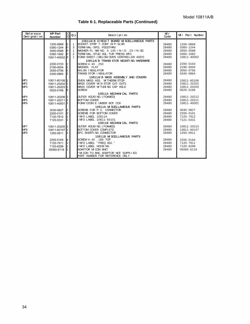
Model 10811A/B
34
Table 6-1. Replaceable Parts (Continued)
Reference Designation
HP Part Number
C D
Qty Description Mfr Code
Mfr Part Number
10811A/B CIRCUIT BOARD MISCELLANEOUS PARTS
1200-0868 5 1 SOCKET-STRP 7-CONT DIP-SLDR 28480 1200-0868
0360-1244 0 3 TERMINAL-SPCL FEEDTHRU 28480 0360-1244
3050-0588 9 1 WASHER-FL NM NO. 6 145-IN-ID .23-IN-OD 28480 3050-0588
0360-1682 0 2 TERMINAL-STUD SGL-TUR PRESS-MTG 28480 0360-1682
10811-40002 4 1 FOAM SHEET-(BELOW OVEN CONTROLLER ASSY) 28480 10811-40002
10811A/B TRANSISTOR MOUNTING HARDWARE
2200-0103 2 SCREW 4-40 .250 28480 2200-0103
2190-0004 2 WASHER, FLAT 28480 2190-0004
3050-0756 2 NYLON INSULATOR 28480 3050-0756
0340-0864 2 TRANSISTOR INSULATOR 28480 0340-0864
10811A/B MASS ASSEMBLY AND COVERS
MP1 10811-60106 1 OVEN MASS ASS. W/THERMISTOR 28480 10811-60106
MP2 10811-20202 1 MASS COVER W/XISTOR CUT-OUTS 28480 10811-20202
MP3 10811-20203 1 MASS COVER W/TUNING CAP HOLE 28480 10811-20203
0520-0166 8 SCREW 28480 0520-0166
10811A MECHANICAL PARTS
MP4 10811-20206 1 OUTER HOUSING (FOAMED) 28480 10811-20212
MP5 10811-20211 1 BOTTOM COVER 28480 10811-20211
MP6 10811-40001 1 FOAM COOKIE UNDER BOT COV 28480 10811-40001
10811A MISCELLANEOUS PARTS
3030-0827 2 SCREWS FOR P.C. CONNECTOR 28480 3030-0827
2200-0101 3 SCREWS FOR BOTTOM COVER 28480 2200-0101
7120-7912 1 INFO LABEL 10811A 28480 7120-7912
7120-0331 1 INFO LABEL 10811-60101 28480 7121-0331
10811B MECHANICAL PARTS
MP7 10811-20205 1 OUTER HOUSING (FOAMED) 28480 10811-20213
MP8 10811-60107 1 BOTTOM COVER COMPLETE 28480 10811-60107
MP9 1250-0911 1 EFC SHORTING CONNECTOR 28480 1250-0911
10811B MISCELLANEOUS PARTS
2200-0164 4 SCREW 4-40 .188 TOP 28480 2200-0164
7120-7911 1 INFO LABEL "FREQ ADJ." 28480 7120-7911
7120-6299 1 INFO LABEL HOUSING 28480 7120-6299
05060-6116 1 ADAPTOR MICON-BNC* 28480 05060-6116
*MICON TO BNC ADAPTOR NOT SUPPLIED.
PART NUMBER FOR REFERENCE ONLY.

Model 10811A/B
35
Table 6-2. Manufacturers Code List
MFR. NO. MANUFACTURER NAME ADDRESS ZIP CODE
00000 ANY SATISFACTORY SUPPLIER
03888 KDI PYROFILM CORP WHIPPANY, NJ 07981
04713 MOTOROLA SEMICONDUCTOR PRODUCTS PHOENIX, AZ 85062
07263 FAIRCHILD SEMICONDUCTOR DIV MOUNTAIN VIEW, CA 94042
24546 CORNING GLASS WORKS (BRADFORD) BRADFORD, PA 16701
25088 SIEMENS CORP ISELIN, NJ 08830
27014 NATIONAL SEMICONDUCTOR CORP SANTA CLARA, CA 95051
28480 HEWLETT-PACKARD CO CORPORATE HQ PALO ALTO, CA 94304
30983 MEPCO/ELECTRA CORP SAN DIEGO, CA 92121
51642 CENTRE ENGINEERING INC STATE COLLEGE, PA 16801
72982 ERIE TECHNOLOGICAL PRODUCTS INC ERIE, PA 16512

Model 10811A/B
36
Page Intentionally Left Blank
Model 10811A/B
37
SECTION VII
MANUAL CHANGES
7-1. INTRODUCTION 7-2. This section contains information necessary to adapt this manual to apply to older instruments.
7-3. MANUAL CHANGES 7-4. This manual applies directly to Model 10811AlB Quartz Crystal Oscillators with serial prefix number 2028.
7-5. NEWER INSTRUMENTS 7-6. As engineering changes are made, newer instruments may have serial prefix numbers higher than those listed on the title page of this manual. The manuals for these instruments will be supplied with "Manual Changes" pages containing the required information to update the manual. Replace affected pages or modify existing manual information as described in the "Manual Changes" pages. See Section VI of this manual for a description of board identification. If the series number etched or stamped on any circuit board or circuit board assembly is higher than the above serial prefix number, "Manual Changes" pages should accompany the manual. 7-7. If the "Manual Change" pages are missing from any HP manual, the information can be supplied by any Hewlett-Packard Sales and Service Office listed at the back of this manual.

Model 10811A/B
38
Page Intentionally Left Blank

Model 10811A/B
39
SECTION VIII
SERVICE
8-1. INTRODUCTION 8-2. This section contains theory of operation, a detailed troubleshooting procedure, and a schematic
diagram.
8-3. SCHEMATIC DIAGRAM SYMBOLS AND REFERENCE DESIGNATORS 8-4. Figure 8-1 shows the symbols used in the schematic diagram. At the bottom of Figure 8-1, the
system for reference designators, assemblies, and subassemblies is shown.
8-5. REFERENCE DESIGNATORS
8-6. Theory of Operation 8-7. The overall theory of operation for the 10811A/B starts with paragraph 8-9. The detailed theory of
operation starts with paragraph 8-13.
8-8. OVERALL BLOCK DIAGRAM THEORY 8-9. The 10811A/B Quartz Crystal Oscillator is an extremely stable, compact, low-power source of 10
MHz. The crystal, along with the oscillator, circuit buffer amplifier, and oven control circuits are all mounted inside a thermally insulated housing.
8-10. A detailed block diagram of the 10811A/B oscillator is shown in Figure 8-2.
8-11. The 10811A/B oscillator is divided into three sections with each section connected by a .010-inch thick flexible circuit. Three small circuit boards are bonded to the flexible circuit to provide support in the areas where components are located. The arrangement allows the unit to be easily disassembled and operated in the disassembled state on the service bench.
8-12. The three sections can be divided into the following subsections (Figure 8-2):
1. Main Oscillator 2. Automatic Gain Control
Voltage Reference (+5.7V and +6.4V) Output Impedance Matching Buffer
3. Output Buffer Amplifier Oven Controller

Model 10811A/B
40
Figure 8-1. Schematic Diagram Notes

Model 10811A/B
41
• A GROUND POINT FOR TESTING OSCILLATOR. AGC,OUTPUT AMPLIFIER AND VOLTAGE REFERENCE.
• B GROUND POINT FOR
TESTING OVEN CONTROLLER.
• B GROUND POINT FOR
TESTING OVEN CONTROLLER.
• A AND B GROUNDS MAY BE
TIED TOGETHER OR FLOATED AT DIFFERENT POTENTIALS EXTERNAL TO THE OSCILLATOR.
Figure 8-2. 10811A/B Overall Block Diagram

Model 10811A/B
42
8-13. MAIN OSCILLATOR THEORY OF OPERATION 8-14. The 10811A/B oscillator is a Colpitts-type crystal oscillator which uses the crystal as the series
inductor. Figure 8-3A shows the basic block diagram of a Colpitts-type oscillator. Figure 8-3B shows the basic equivalent components of the oscillator.
Figure 8-3A. Basic Colpitts- Type Oscillator
r
Figure 8-3B. Main Oscillator Schematic Design
8-15. Comparing Figure 8-3A and 8-3B, we find Y1 is the inductor, capacitor CA is C8 and CB is the combination of C5, L2, C6, and L3. C5 is a dc blocking capacitor. Its reactance is very low, so the combination of these components can be redrawn as in Figure 8-4. The crystal Y1 is a "third overtone" crystal and is operated at 10 MHz. To keep the circuit from oscillating at the crystal's fundamental, or at a different overtone, the mode suppression network of C5, L2, C6, L3 appears capacitive only at frequencies between 9 MHz and 10.5 MHz. Below and above this frequency range, the network appears inductive. This does not allow the proper phase shift around the loop and thus suppresses oscillations at all frequencies other than 10 MHz. It should be noted that any reactance in series with the crystal will cause a change in frequency.

Model 10811A/B
43
Figure 8-4. Mode Suppression
8-16. Figure 8-5 show the equivalent crystal circuits with the tuning capacitor C1.
Figure 8-5. Frequency Tuning Circuit
8-17. C1 tuning capacitor is available from the top of the oscillator outer housing. The change in reactance of C1 allows the oscillator's frequency to be varied over a 20 Hz (2 X 10⁻⁶) range. C9 and C4 are dc blocking capacitors.
8-18. ELECTRONIC FREQUENCY CONTROL (EFC) 8-19. To allow for a fine tuning control, a varactor (CR1) is added in parallel with C1 tuning capacitor.
See Figure 8-6. The varactor's capacitance depends on the dc voltage applied to it (reverse bias). The HC voltage range is +5 volts to -5 volts, giving a fine tuning range of ≈1 Hz (1 X10⁻⁷). Since one side of the varactor is tied to a reference (6.4V), a full +5 volts applied to the HC input will still keep CR1 reverse biased. C2 and C3 are again dc blocking capacitors to keep the HC current from flowing in to the crystal circuit. Note: if the HC input is not used, it must be connected to ground to keep any noise from modulating the HC line and causing frequency changes.

Model 10811A/B
44
Figure 8-6. EFC
8-20. AUTOMATIC GAIN CONTROL (AGC) 8-21. The output for the AGC (and output amplifiers, discussed later) is taken across capacitor C10,
and is applied to Q3. Since C10 is effectively in series with the crystal, the current passing through the crystal also passes through C10. The voltage across C10 is therefore proportional to the current through the crystal. As the output of the oscillator changes, the output of the peak detector circuit changes. This change in the AGC voltage changes the voltage applied to the base of Q1 and stops the impending output voltage change. A peak detector circuit formed by C12, CU, CR4 and CR5 is used to develop a dc voltage to control the crystal current. This negative control voltage forms the lower half of a voltage divider for the base of Q1 (R6 and R7). Controlling the bias current and the gain of Q1. Thus AGC action controls the output signal level. (See Figure 8-7).
Figure 8-7. Automatic Gain Control (AGC)
8-22. By adjusting the AGC voltage with R6 the amplitude for the output (at the base of Q3) can be set.
R5 sets the AGC limit when R6 is at its minimum resistance.

Model 10811A/B
45
8-23. RF OUTPUT IMPEDANCE MATCHING AND OUTPUT BUFFER 8-24. The signal for the output amplifiers is taken from the same point as the AGC (across C10). The
voltage is buffered by Q5 which is an impedance matching stage. Resistors R14 and R15 set the dc bias level while C14 allows the ac to bypass R14. The signal is then applied to the output buffer stage of Q9. Resistor R40 provides the 50Ω source impedance when transformed by T1. Typical gain from Q9 base to collector is approximately 2. See Figure 8-8.
Figure 8-8. Output Amplifiers
8-25. VOLTAGE REFERENCES (5.7V AND 6.4V) 8-26. Constant current diode CR2 feeds 1 mA to zener diode CR3 providing 6AV dc for the EFC
varactor reference. R12 and C15 form a filter to attenuate noise from the zener diode. R13 provides current limiting for Q5 if the 5.7V line is shorted. See Figure 8-9.

Model 10811A/B
46
Figure 8-9. Voltage References
8-27. OVEN HEATER AND CONTROLLER THEORY NOTE
In the following theory of operation the term OVEN MASS will be used to describe the cast aluminum block in which the crystal and crystal electronics are located. The exploded view of the oscillator shows the oven mass.
8-28. The purpose of the oven is to shield the oscillator crystal and electronics from normal ambient temperature changes. The oven controller does this by maintaining a constant oven temperature which is higher than the highest expected ambient temperature.
8-29. Three main blocks make up the oven circuits. See Figure 8-10.
1. Thermistor 2. Amplifier (controller) 3. Heaters
8-30. In the 10811A/B oven, a thermistor (RT1) is secured with epoxy into a hole in the oven mass. U3
is the amplifier and Q7 (not shown) and Q8 are the heaters. It is the thermistor that senses the oven mass temperature. Since it is in one leg of the bridge circuit, when the mass temperature changes slightly, a voltage change occurs across the bridge (RT1, R18, R19, R20, R21). Amplifier U3 boosts this voltage change and then uses it to control the current through Q7 and Q8. The current flowing through transistors Q7 and Q8 causes power dissipation in the form of heat, and it is this heat that warms the oven mass. Therefore, when the mass temperature starts to change, the heaters are told to adjust their power to cancel the impending temperature change.
8-31. WARM-UP: GENERAL OPERATION. If the oscillator has been off for several hours, the mass
and thermistor will be at the ambient temperature. Assuming this is below the normal oven operating temperature (80 to 84°C) the resistance at the thermistor RT1 is higher than that of R18 + R20 and therefore V1 > V2. This causes the output of U3 to be ≈ (Vcc - 1.5V) and supply base current to Q8 through Q6. A separate circuit limits the collector current of Q8 and is described later. As the oven mass warms up, the thermistor's resistance gets lower causing both V2 and V1 to lower (V2 lowers because Vo lowers due to RT1 getting smaller). V1 decreases at a faster rate than V2 and eventually V1 = V2 when RT1 = R20 + R18. At this time, the oven controller "cuts back" and begins to operate in a linear mode, adjusting the collector current in Q8 (and therefore the power dissipated in Q7 and Q8) to keep the oven precisely at its set temperature.
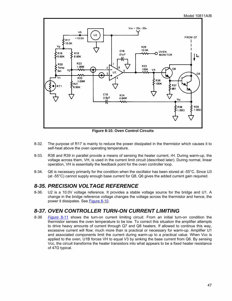
Model 10811A/B
47
Figure 8-10. Oven Control Circuits
8-32. The purpose of R17 is mainly to reduce the power dissipated in the thermistor which causes it to self-heat above the oven operating temperature.
8-33. R38 and R39 in parallel provide a means of sensing the heater current, rH. During warm-up, the voltage across them, VH, is used in the current limit circuit (described later). During normal, linear operation, VH is essentially the feedback point for the oven controller loop.
8-34. Q6 is necessary primarily for the condition when the oscillator has been stored at -55°C. Since U3 (at -55°C) cannot supply enough base current for Q8, Q6 gives the added current gain required.
8-35. PRECISION VOLTAGE REFERENCE 8-36. U2 is a 10.0V voltage reference. It provides a stable voltage source for the bridge and U1. A
change in the bridge reference voltage changes the voltage across the thermistor and hence, the power it dissipates. See Figure 8-10.
8-37. OVEN CONTROLLER TURN-ON CURRENT LIMITING 8-38. Figure 8-11 shows the turn-on current limiting circuit. From an initial turn-on condition the
thermistor senses the oven temperature to be low. To correct this situation the amplifier attempts to drive heavy amounts of current through Q7 and Q8 heaters. If allowed to continue this way, excessive current will flow; much more than is practical or necessary for warm-up. Amplifier U1 and associated components limit the current during warm-up to a practical value. When Vcc is applied to the oven, U1B forces VH to equal V3 by sinking the base current from Q6. By sensing Vcc, the circuit transforms the heater transistors into what appears to be a fixed heater resistance of 47Ω typical.

Model 10811A/B
48
Figure 8-11. Turn-on Current Limit Circuit
8-39. HEATER TRANSISTOR BALANCE 8-40. Because heater transistors Q7 and Q8 are not equally spaced from the crystal, it is necessary to
offset the power dissipation between the two transistors. Figure 8-12 shows a simplified schematic of this circuit. Amplifier U1A references a voltage divider across Vcc (R25, R26) and a divider referenced to the mid-point between the heater transistors. From this U1A controls the base current of Q7 to insure the Voltage at the mid-point between the heater transistors is a constant percentage of Vcc (V4 ≈ 0.57 Vcc ± 2%).
Figure 8-12. Heater Transistor Balance Circuit.

Model 10811A/B
49
8-41. REPAIR AND TROUBLESHOOTING
8-42. Inspection 8-43. The 10811A/B should be inspected for indications of mechanical and electrical defects. Electronic
components that show signs of overheating, leakage, frayed insulation, and other signs of deterioration should be checked and a thorough investigation of the associated circuitry should be made to verify proper operation. Mechanical parts should be inspected for excessive wear, looseness, misalignment, corrosion, and other signs of deterioration.
CAUTION Proper static handling techniques must be employed when servicing semiconductor products. The voltage susceptibility of all IC and transistor families is well below levels commonly found in service environments. Exercise care and observe standard static precautions.
8-44. REPAIR
8-45. Printed Circuit Component Replacement 8-46. To prevent damage to the plating and the replacement component, apply heat sparingly, and
work carefully. See CAUTION below.
8-47. Replacing Integrated Circuits 8-48. Following are two recommended methods of replacing integrated circuits:
a. SOLDER GOBBLER. This is the best method. Solder is removed from board by a soldering iron with a hollow tip connected to a vacuum source.
b. CLIP-OUT. Clip the leads as close to the component as possible. With a soldering iron and long nose pliers, carefully remove the leads from each hole. Then clean the holes.
CAUTION The flex circuitry used in the 10811A/B oscillator requires special attention to soldering iron tip temperature and the length of time heat is applied. A low wattage (≈25W) iron with a temperature control should be used. The tip temperature should be held below 500°C. Care should be taken to be sure that the iron is not held on the circuit longer than necessary. Components should be removed by clipping the leads and then gently removing them. Do not use force when removing components. Following these precautions will insure that repairs can be easily made without damaging the flex circuit. Also, components should not be arbitrarily removed for troubleshooting or replacement unless there is reasonable confidence in the component's failure.

Model 10811A/B
50
WARNING THE OSCILLATOR'S INTERNAL OVEN MASS TEMPERATURE MAY BE AS HIGH AS 85°C (185°F). TO AVOID SERIOUS BURNS DO NOT REMOVE OSCILLATOR CIRCUITS AND/OR OVEN MASS ASSEMBLY FROM THE OUTER CAN UNTIL THE OSCILLATOR HAS SUFFICIENTLY COOLED (APPROXIMATELY ONE HOUR WITH BOTTOM COVER AND FOAM INSULATOR REMOVED). THE OUTER HOUSING TEMPERATURE IS NOT A RELIABLE INDICATION OF THE INTERNAL TEMPERATURE.
8-49. The troubleshooting is arranged to allow the technician to quickly find the defective component(s)
without unnecessary removal of components.
8-50. TROUBLESHOOTING 8-51. Failures in the 10811A/B can be divided into two sections:
1. Failure of the oscillator's circuits.
2. Failure in the oven controller circuits.
8-52. Failures in the oscillator circuits can be divided into the following problems:
1. No output.
2. Output amplitude is too low or high.
3. Output is distorted (contains excessive harmonics).
4. Output is off frequency (high or low).
5. Output has excessive noise or frequency stability does not meet specifications.
8-53. Poor frequency stability can be difficult to troubleshoot, and many times the oscillator is not at fault. Environmental conditions can affect stability and should be ruled out first.
8-54. Failures in the oven circuitry can be divided into the following problems:
1. No oven current (heat).
2. Excessive oven current (>600 mA).
3. Oven does not cut back after warm-up (this will open the thermal fuse if allowed to continue).
4. Oven does not regulate at the proper temperature. (This can be the cause for poor frequency stability).
8-55. Since the main oscillator and oven control power supply inputs are separate from each other, the defective circuit can be operated without applying power to the complete oscillator.
8-56. Determine which section is defective (oven or oscillator circuit), then proceed as described in the following troubleshooting section. The two circuits can be investigated separately.
1. Remove top cover and insulator described in:
a. 10811A paragraphs 8-59.
b. 10811B paragraphs 8-59, step 4.

Model 10811A/B
51
CAUTION With the cover and foam insulator removed to thermal fuse cannot protect the oven circuit from thermal runaway. Caution should be used at all times.
8-57. DISASSEMBLY FOR TROUBLESHOOTING AND REPAIR 8-58. Perform steps 1 through 3 for the 10811A oscillator and steps 4 and 5 for the 10811B oscillator.
Once these steps are completed, follow steps 6 through 10 for both oscillators.
8-59. For the 10811A Oscillator:
Step 1. Remove the three screws securing the bottom cover to the outer housing, and remove bottom cover.
Step 2. Remove the two screws securing the pc edge connector to the outer housing.
Step 3. Remove the foam sheet to expose the oven controller circuit board.
If troubleshooting the oven controller, stop here and go to paragraph 8-69. Go to Step 6 only if the trouble is in the oscillator circuit.
For the 10811B oscillator:
Step 4. Remove the four screws securing the cover to the outer housing.
Step 5. Disconnect the flexible circuit attached to the cover from the 7-pin connector mounted to the oven controller circuit board.
If troubleshooting the oven controller, stop here and go to paragraph 8-69. Continue only if the trouble is in the oscillator circuit.
The following steps will be performed for both oscillators.
Step 6. Using a long, small diameter tool, remove the complete oscillator assembly by inserting the tool into the tuning capacitor access hole (labeled FREQ. ADJUST) and pushing on the capacitor until the circuit can be grasped and removed freely.
CAUTION 10811A Only
Do not remove the circuits by pulling on the edge connector or flexible circuit. Damage to the flexible circuit may occur.
Step 7. Using a Pozidriv screwdriver , remove the two screws securing the heater transistors to the oven mass. Remove the washers and transistor insulators.
NOTE
When reassembling the oven mass the heater transistor screws must be tightened to a torque of 44 Newton meters (5 in.-Ibs.)
Step 8. Tilt the oven controller assembly back and remove the foam insulator between the oven controller assembly and the oven mass. Be careful not to break the two black thermistor wires attached to the oven controller assembly.
Step 9. Remove the eight screws (four each side) securing the covers to the oven mass assembly.
Step 10. Use two of the screws from each cover (removed in Step 9) to secure the boards to the mass for troubleshooting.

Model 10811A/B
52
8-60. Go to paragraph 8-84, Oscillator Troubleshooting. When reassembling unit, reverse the above procedure.
8-61. SPECIAL TEST CONNECTOR FOR 10811A 8-62. The following paragraphs describe a special 15-pin connector for use in troubleshooting,
alignment and testing of the 10811A. The connector provides the following (See Figure 8-13):
a. Two separate input leads for the oscillator circuits power and the oven heaters and controller circuits.
b. 10 MHz output through a female BNC. c. Oven monitor output for connection to a voltmeter. d. HC input connection to ground.
Figure 8-13. 10811A/B Special Test Connector
8-63. The following parts are required to construct the special test connector:
a. 15-pin pc board connector (HP part number 1251-0494).
b. 6 banana plugs (HP part number 1251-0124).
c. BNC female connector with ground lug and nut.
BNC connector 1250-0083 Ground lug 0360-0024 lock washer 2190-0016 Nut 2950-0001

Model 10811A/B
53
d. Approximately 6-feet of 24-gauge wire.
e. Labels for banana plugs.
8-64. To construct the connector:
a. Solder the center pin of the BNC connector to pin 1(A) of the printed circuit connector; this is the 10MHz output signal.
b. Bend the BNC ground lug to align with pin 2(B) of the printed circuit connector. c. Solder one end of a 2-foot length of wire to pin 2(B) of the printed circuit connector.
Also solder the BNC ground lug to pin 2(B). This is the oscillator circuit common. d. Solder one end of a 2-foot length of wire to pin 3(C) of the printed circuit connector.
This is the oscillator (+) supply. e. Connect a jumper wire between pins 5(E) and 6(F). This terminates the HC input. f. Solder one end of a 2-foot length of wire to pin 11(M). This is oven monitor output. g. Solder one end of a 2-foot length of wire to pin 14(R) of the printed circuit connector.
This is the oven (+) supply. h. Solder one end of two 2-foot lengths of wire to pin 15(S) of the printed circuit connector.
This is the oven common. i. Twist together one of the two wires connected to pin 15(S) and the wire connected to pin
14(R). These are the oven controller power supply inputs. j. Twist together the remaining wire connected to 15(S) and the wire connected to pin 11(M).
This is the oven monitor output. k. Twist together the two wires connected to pins 2(B) and 3(C). These are the oscillator supply
input. l. Connect one banana plug to the free end of each wire. m. Label each banana plug as follows:
Wire connected to: Label as: pin 2(B) oscillator supply (-) pin 3(C) oscillator supply (+) pin 11 (M) oven monitor (+) pin 14(R) oven supply (+) pin 15(S) two wire oven supply (-)
oven monitor (-)
n. Inspect the connector for poor solder joints, bent or damaged pins. Double check the labeling of the banana plugs to be sure the polarity markings are correct. If the voltages are connected the wrong way, damage to the 10811A may occur.
8-65. SPECIAL CABLE FOR THE 10811B. 8-66. A micon to BNC adaptor cable is available for the 10MHz output signal. Order HP Part Number
05060-6116 (see Figure 8-13).
8-67. SPECIAL PARTS REPLACEMENT CONSIDERATIONS 8-68. Several mechanical parts and components must be replaced as a pair or require special
consideration. They are:
a. Oven mass assembly and thermistor: If the thermistor (RT1) is found to be defective, the thermistor and oven mass assembly must be replaced as one item, HP Part Number 10811-60106. Do not attempt to replace the thermistor alone.
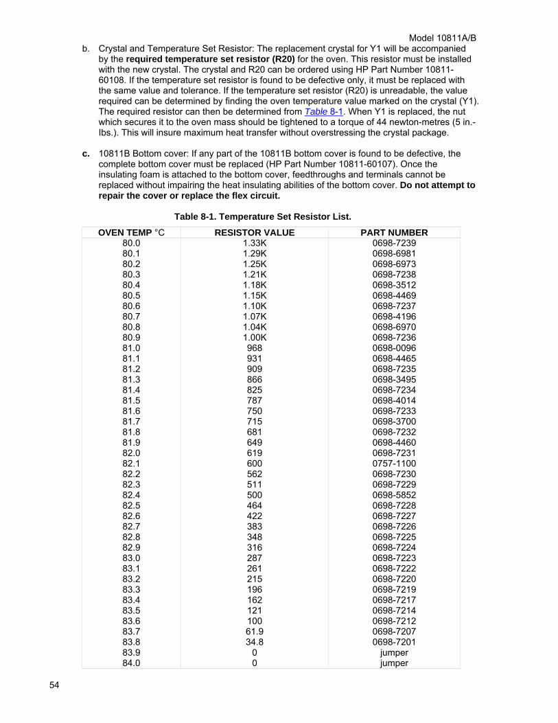
Model 10811A/B
54
b. Crystal and Temperature Set Resistor: The replacement crystal for Y1 will be accompanied by the required temperature set resistor (R20) for the oven. This resistor must be installed with the new crystal. The crystal and R20 can be ordered using HP Part Number 10811-60108. If the temperature set resistor is found to be defective only, it must be replaced with the same value and tolerance. If the temperature set resistor (R20) is unreadable, the value required can be determined by finding the oven temperature value marked on the crystal (Y1). The required resistor can then be determined from Table 8-1. When Y1 is replaced, the nut which secures it to the oven mass should be tightened to a torque of 44 newton-metres (5 in.-Ibs.). This will insure maximum heat transfer without overstressing the crystal package.
c. 10811B Bottom cover: If any part of the 10811B bottom cover is found to be defective, the
complete bottom cover must be replaced (HP Part Number 10811-60107). Once the insulating foam is attached to the bottom cover, feedthroughs and terminals cannot be replaced without impairing the heat insulating abilities of the bottom cover. Do not attempt to repair the cover or replace the flex circuit.
Table 8-1. Temperature Set Resistor List.
OVEN TEMP °C RESISTOR VALUE PART NUMBER 80.0 1.33K 0698-7239 80.1 1.29K 0698-6981 80.2 1.25K 0698-6973 80.3 1.21K 0698-7238 80.4 1.18K 0698-3512 80.5 1.15K 0698-4469 80.6 1.10K 0698-7237 80.7 1.07K 0698-4196 80.8 1.04K 0698-6970 80.9 1.00K 0698-7236 81.0 968 0698-0096 81.1 931 0698-4465 81.2 909 0698-7235 81.3 866 0698-3495 81.4 825 0698-7234 81.5 787 0698-4014 81.6 750 0698-7233 81.7 715 0698-3700 81.8 681 0698-7232 81.9 649 0698-4460 82.0 619 0698-7231 82.1 600 0757-1100 82.2 562 0698-7230 82.3 511 0698-7229 82.4 500 0698-5852 82.5 464 0698-7228 82.6 422 0698-7227 82.7 383 0698-7226 82.8 348 0698-7225 82.9 316 0698-7224 83.0 287 0698-7223 83.1 261 0698-7222 83.2 215 0698-7220 83.3 196 0698-7219 83.4 162 0698-7217 83.5 121 0698-7214 83.6 100 0698-7212 83.7 61.9 0698-7207 83.8 34.8 0698-7201 83.9 0 jumper 84.0 0 jumper

Model 10811A/B
55
d. Oven heater transistors Q7 and Q8: The replacement transistors for Q7 and Q8 have formed
leads for easy installation (Part Number 10811-80001). Holding screws for Q7 and Q8 must also be torqued to a specific force of 44 newton-metres (5 in.-Ibs.). There are several
available Pozidriv torquing screwdrivers.
8-69. OVEN CONTROLLER TROUBLESHOOTING
8-70. General 8-71. The oven controller section consists of three major circuits and a 10V voltage reference for
increased stability of sensitive circuits. Figure 8-14 shows the major circuits and active components involved in their operation.
8-72. The temperature sense circuit monitors the temperature of the oven mass and reduces the power drawn by the oven heater transistors when the oven mass has reached operating temperature. After power cut-back, this circuit monitors the oven mass temperature and controls the power in the heaters to maintain the constant temperature. The thermistor (RT1) has a negative temperature coefficient. At room temperature the thermistor resistance is approximately 100K ohms, while at operating temperature (-82°C) the resistance is approximately 9K ohms. Shorting the thermistor to oven common makes the oven mass appear too hot to the temperature sense circuit. This in turn causes the temperature sense circuit to shut off power to the oven heaters. This technique is used in the troubleshooting procedure.
8-73. The warm-up current limit circuit controls the maximum current the oven may draw during warm-up (380 to 490 mA with 20V dc oven input). This circuit is only active during the warm-up phase of the oven circuit operation.
Figure 8-14. Oven Controller Block Diagram

Model 10811A/B
56
8-74. Normal Operation 8-75. When the oven is tested under normal conditions (-25°C ambient temperature) it will initially draw
380 to 490 mA. After 5 to 10 minutes the oven current will start to drop. Over the next 10 to 15 minutes the oven current will fall to the 60 to 150 mA range where it will stabilize. The oven circuit should not oscillate.
WARNING DO NOT OPERATE THE OVEN CIRCUITS WHEN THE OVEN MASS IS OUTSIDE OF THE OSCILLATOR INSULATED HOUSING. DOING SO WILL OVERHEAT THE OSCILLATOR CIRCUITS INSIDE THE OVEN MASS AND CAUSE PERMANENT DAMAGE. ALL OVEN TEST POINTS ARE AVAILABLE WITH THE OVEN MASS AND OVEN CONTROLLER CIRCUIT INSIDE THE HOUSING. WHEN OSCILLATOR COVER AND INSULATOR ARE REMOVED THERMAL FUSE WILL NOT PROTECT CIRCUIT FROM OVERHEATING. APPLY OVEN POWER ONLY WHEN ACTUALLY MAKING MEASUREMENTS FOR TROUBLESHOOTING OR AS DIRECTED IN TROUBLESHOOTING TREE, TABLE 8-2.
8-76. TROUBLESHOOTING 8-77. Table 8-2 is a troubleshooting' tree for the oven circuits. The troubleshooting procedure separates
the different functional circuits by monitoring the oven supply current during different operating conditions. For example, if the warm-up current is excessive, this indicates a trouble in the warm-up current limit circuit, or the current control and heater circuit. If shorting the thermistor reduces the current being drawn from the power supply, this indicates the current control circuit is operating and the problem is most likely in the warm-up current limit circuit.
8-78. As with most troubleshooting trees this is intended to be a guide to the trouble area. It is not a substitute for technical skill in isolating the faulty components.
8-79. Table 8-3 (next to schematic diagram) gives normal circuit voltages during warm-up, operation, and when thermistor RT1 is shorted to ground. Use this table during troubleshooting.
8-80. Troubleshooting Cautions 8-81. When oven current is excessive, turn on the power supply only long enough to make the
necessary measurements. Do not leave power on if the oven is drawing excessive current. With the housing cover and foam insulator removed, the thermal fuse (F1) cannot protect the circuits in the oven mass from overheating and damage.
8-82. Flex Damage 8-83. If a tear in the flex circuit occurs, the tear can continue until a trace is broken. To stop a tear, use
a pair of scissors and cut around the tear. DO NOT CUT A SHARP CORNER as this will cause a stress concentration allowing the tear to start again. A hole-punch may also be used. Punch a hole in the flex so as to remove the forward end of the tear.

Model 10811A/B
57
Table 8-2. Oven Controller Troubleshooting Tree

Model 10811A/B
58
8-84. OSCILLATOR TROUBLESHOOTING 8-85. The oscillator circuits are relatively simple and straightforward. The following paragraphs will
briefly describe the major circuit areas, a troubleshooting outline, and some helpful suggestions to make the troubleshooting process easier. The oscillator consists of four sections. They are:
1. Oscillator Q1, Q2, and associated circuitry. 2. AGC Q3, CR4, CR5, and R6. 3. Output circuit Q5, Q9. 4. 5.7V power supply CR2, CR3, and Q4.
The oscillator is the signal source. Its output level is controlled by the AGC. The 5.7V power supply provides an extra-stable clean voltage source for the oscillator circuits. The output circuits provide a high level signal capable of driving a 50 to 1K ohm load.
8-86. NORMAL OPERATION 8-87. The output of the oscillator circuit at Q2(C) is a 10 MHz undistorted sine wave; with an amplitude
of approximately 2.8V p-p. The AGC voltage (measured at CR5-C13 junction) is approximately -1.5V. The 10 MHz signal passes through Q5 to Q9(B) at about the same level. The voltage gain of amplifier Q5 (base to collector) is approximately 2 with a 50-ohm load on the output. The output of transformer T1 is approximately 1.5V p-p. All10 MHz signals found in the 10811A/B will be undistorted sine waves unless otherwise noted in Table 8-4 (next to the schematic diagram).
8-88. OSCILLATOR TROUBLESHOOTING TECHNIQUES 8-89. When troubleshooting the oscillator section, remove the oven mass from the housing and the
covers from the oven mass as described in paragraph 8-59. Connect 12V to the oscillator section; use special connector described in paragraph 8-61 for 10811A, connect power to T1(1) and oscillator circuit common in 10811B. Set the power supply current limit to 60 mA. Do not apply power to the oven circuits!
8-90. Initial troubleshooting and probing should be done on the backside of the boards (trace side)
while they are secured to the oven mass (see paragraph 8-59, step 10). This way the circuits are more easily handled. When the fault is isolated to a few components, the unit may then be disassembled for final troubleshooting and repair.
8-91. Helpful Hints
1. Most points in the oscillator circuits cannot be measured with a dc voltmeter. The reactance of the voltmeter probe and leads will load the circuit and give false readings. Instead, use an oscilloscope with a high input impedance probe for these measurements. Table 8-4 (oscillator section normal voltages) indicates when a dc voltmeter can be used.
2. Before reinstalling the oven mass into the housing, adjust the output amplitude (with R6) to 0.53V into a 50-ohm load. Although this value is slightly below normal, the output will increase slightly when the unit is reassembled and is at normal operating temperatures.
3. If a tear in the flex circuit occurs, go to paragraph 8-82 for repair instructions.

Model 10811A/B
59
8-92. TROUBLESHOOTING INFORMATION 8-93. Symptoms of failures in the oscillator sections will generally fall into one of the following
categories:
1. No output. 2. Output amplitude is low or high. 3. Output is distorted (contain excessive harmonics). 4. Excessive drift of output frequency. 5. Time domain frequency stability (short-term stability) does not meet specifications.
8-94. Troubleshooting of these faults will be discussed in the following paragraphs.
8-95. NO OUTPUT. This is usually easy to repair by simple signal tracing. Localized faultfinding (to actual defective component) can be somewhat more difficult if the problem is in the main oscillator circuit (Q1, Q2, and AGC). If the fault appears to be in the oscillator section and does not yield to normal troubleshooting techniques, measure the AGC voltage at the junction of CR5-C13 (see Note 7 on Table 8-4, Oscillator Normal Voltages). If this voltage appears normal, the problem may be a defective quartz crystal (Y1). To verify this possibility, obtain a 10 µH (HP Part No. 9100-2265) and a 12 µH inductor (9100-2242). Use the HP numbered parts as these have been tested in the circuit. On the oscillator board, remove the red and blue wires connecting the crystal to the board. Place the 12 µH inductor in place of these wires. With 12V applied to the circuit, adjust the FREQ ADJUST (C1), and amplitude control (R6) for a good sine wave signal.
NOTE At some settings of C1 and/or R6, intermittent oscillations may appear. Some minor adjustment of C1 and/or R6 should clear this. If this fails, replace the 12 μH inductor with the 10 μH inductor and repeat the C1/R6 adjustment.
If replacing the crystal with an inductor produces oscillation, this is a very good indication of a defective crystal. When replacing crystal Y1, read paragraph 8-68(b), Special Parts Considerations. If the circuit will still not oscillate, the problem is most likely one of the oscillator circuit elements.
8-96. OUTPUT AMPLITUDE HIGH OR LOW. Many times this can be cured by the adjustment of R6 as
described in paragraph 5-14. If the correct amplitude cannot be obtained with this adjustment, monitor the signal at Q6(C) with an oscilloscope and set R6 to obtain an amplitude of 2.8V p-p. Then check Q5 and Q9 stages. If the R6 adjustment isn't effective, you should suspect the AGC circuitry (Q3, CR4, CR5, C5, C6, R5, R6, R7, or Q1).
8-97. OUTPUT DISTORTION. Check the distortion with a spectrum analyzer (see Table 4-2 step 2. for procedure). If the distortion products are harmonically related to 10 MHz, trace the signal to the distorting stage. If the distortion is not harmonically related to the 10 MHz output:
1. Check the mode suppression components of L2/C5 and/or L3/C6. These components suppress oscillations at all frequencies other than 10 MHz.
2. Check for spurious oscillations from the amplifier stages and oscillator transistors. 8-98. EXCESSIVE DRIFT OF OUTPUT FREQUENCY. When a quartz crystal oscillator has not been
operated for a long period of time, or if it has been subjected to severe thermal or mechanical shock, the oscillator may take some time to stabilize. In most cases, the crystal will drift and then stabilize at or below the specified rate within a few days after being turned on. In isolated cases, depending on the amount of time the oscillator has been off and the environmental conditions it has experienced, the 10811A/B may take up to 1 week to reach the specified aging rate. This should be taken into consideration if the drift rate of the unit is out of specifications. If the unit has had sufficient time to stabilize but is still out of specification, the most likely cause of excessive drift is a defective crystal (Y1). If Y1 is to be replaced, read paragraph 8-68(b). Other possible causes are unstable C3 and/or C8.

Model 10811A/B
60
8-99. TIME DOMAIN STABILITY (SHORT-TERM STABILITY) OUT OF SPECIFICATION. Measurement of time domain stability is somewhat difficult and exacting. If the 10811A/B fails this test, be sure no signal sources other than the test reference are operating near the measurement system, as these can cause interference with the measurement. Other sources of error are vibration, nearby electrical equipment, poor shielding, or motors that can radiate signals into the 10811A/B. The failure to connect the HC input (to ground) can cause poor frequency stability as can a noisy voltage being used for the EFC control. If another oscillator is available (known to be good), verify the accuracy of the measurement system. This could save considerable troubleshooting time.
8-100. Two other possibilities external to the oscillator are the oven and oscillator power supplies. These
must be stable in order for the circuits to function properly. See Table 1-1, Specifications, and paragraph 2-6 for power supply noise requirements.
8-101. When troubleshooting this condition, carefully monitor the output waveform. Check for distortion
or intermittent distortion, small amplitude variations (there should be none), or spurious oscillations on the output signal. Use a spectrum analyzer for this test (see Table 4-2, step 3). These symptoms can be more readily traced than small frequency fluctuations.
8-102. Almost any of the circuits can cause poor short-term stability. However, the most probable cause
is crystal Y1. Other possible causes are the oven controller circuit (keeps changing temperature) or defective frequency determining components (CR1, C1, C3, C8, or instability in the 5.7V supply). Q1 and Q2 are also good suspects. Instability can also be caused by the AGC circuit, but this is usually visible as output amplitude variations or instability on the output waveform.
8-103. To check oven stability, allow the 10811A/B to operate normally away from drafts or sudden
temperature changes. Allow the unit to warm up for at least 1-hour then connect a sensitive recorder or digital voltmeter to the OVEN MONITOR OUTPUT. Once the oven has stabilized, the monitor voltage should not vary more than 100-200 µV when measured over 3- to 4-minute periods. Causes of oven instability are temperature sensing elements RT1, U2, U3, and associated components.

Model 10811A/B
61
Table 8-3. Oven Circuit Voltages·
OVEN AT OVEN COLD (JUST RT1 VOLTAGE POINT OPERATING TEMP. AFTER TURN-ON) GROUNDED
Q6B 1.6 2. .25 Q6C 11.4 11.4 11.4 Q6E 1. 1.3 0 Q7B 12.5 12.7 11.9 Q7C 20. 20. 20. Q7E 11.4 11.4 11.4 Q8B 1. 1.3 0 Q8C 11.4 11.4 11.4 Q8E .07 .23 0
U1 Pin 1 8.9 1.8 8.9 U1 Pin 2 .07 .23 0 U1 Pin 3 .2 .23 .2 U1 Pin 5 4. 4.1 3.8 U1 Pin 6 4. 4.1 3.8 U1 Pin 7 3.3 4.8 1.5 U2 Pin 2 10. 10. 10. U3 Pin 6 3.5 19.0 .5
*Voltage readings taken with oven supply voltage of 20V dc and insulating foam and cover removed. Voltages are approximate and will vary slightly from unit-to-unit.
Table 8-4. Oscillator Section Normal Voltages (see Notes 1, 2, 3)
NORMAL VOLTAGES
VOLTAGE POINT
AC (p-p) DC REMARKS
C3/R3 1 to 4 - Note 8 CR5/C13 - -1.5 Notes 4 and 7 CR3(C) 0 6.3 Note 4 Q1(B) 1 .75 Note 8 Q1(C) 0 5.5 Note 4 Q1(E) .9 .03 Note 8 Q2(B) 0 2.7 Note 4 Q2(C) 2.7 5.6 Note 8 Q2(E) .06 2 Notes 4 and 5 Q3(B) 2.7 5.6 Note 8 Q3(C) 0 11.8 Note 4 Q3(E) 2.4 4.9 Notes 4 and 6 Q4(B) 0 6.3 Note 4 Q4(C) 0 10.3 Note 4 Q4(E) 0 5.6 Note 4 Q5(B) 2.7 3.1 Note 8 Q5(C) 0 11.8 Notes 8 and 9 Q5(E) 2.8 2.6 Note 8 Q9(B) 2.8 2.8 Note 8, 9 Q9(C) 5.1 11.8 Note 8, 9 Q9(E) 2.5 1.9 Note 8
NOTES: 1. All voltages taken with 12V oscillator supply. 2. Voltages are approximate and will vary slightly from unit-to-unit. 3. All ac voltages are sine waves except Q2(E) and Q3(E). 4. This dc voltage may be measured with a standard dc voltmeter. All other voltages should be measured with an
oscilloscope and high impedance probe to minimize circuit loading. 5. Waveform is 6. Waveform is slightly flattened on the bottom. 7. This is the AGC voltage. Value shown is nominal with oscillator operating. If the oscillator is not oscillating, the
AGC voltage will be -+2.5V. 8. Measure both ac and dc voltages with an oscilloscope and a high impedance probe to minimize circuit loading. 9. AC voltage at Q9(C) measured with 50-ohm load on the output.

Model 10811A/B
62
Page Intentionally Left Blank

Model 10811A/B
63

Model 10811A/B
64
Figure 8-15. Oven Controller Schematic Diagram

Model 10811A/B
65

filename: (90027-1) (R. Mejia-Norton October 26, 1999 10:27 AM)
DWG. NO. A-10811-90027-1 REV.H PAGE 1 OF 27
REVISION PAGE
1. This page records a running history of all changes to this procedure.
2. Rev. A is used to identify the first issue. Subsequent changes to the procedure areidentified with letters in the revision column.
3. Description column should include brief before/after details of each change andthe page number involved.
4. Every page in this procedure must have, in order, the drawing number, latestrevision letter and page # of # located in the page footer.
Rev. PCO No. Page No.Affected
Description of Change Engineer Date
A AS ISSUED L. Fries 11-30-90B 2-21684 All Complete Rewrite D. Montgomery 01-20-94C 2-22408 10,19-22 Corrected Osc. # on pg.10.
Added pages 19-22. D. Montgomery 11-27-95
D 2-22774 Sections12,13,14,15
updated specs. for-60158/60159/60160;added 10811-60164
D. Montgomery 10-16-96
E 2-23023 17,25 Added 10811-60260 D. Montgomery 05-01-97F 2-23915 15 Updated index. D. Montgomery 06-10-99
G 2-24149 15,16 Updated index. D. Montgomery 10-26-99H 2-24428 Section 11 Add Phase Noise Specs
for 10811-60219D. Montgomery 07-17-00
Document Owner: PFS Production Manager or Designate

2TABLE OF CONTENTS
TABLE OF CONTENTS . . . . . . . . . . . . . . . . . . . . . . . . . . . . . . . . . . . . . . . . . . . . . . . . . . . . . . . . . . . . 2. . . . . . .1 10811D/E Crystal Oscillators . . . . . . . . . . . . . . . . . . . . . . . . . . . . . . . . . . . . . . . . . . . . . . . . . . . . . . 3. . . . . . .2 10811D/E Option 001 . . . . . . . . . . . . . . . . . . . . . . . . . . . . . . . . . . . . . . . . . . . . . . . . . . . . . . . . . . . . . 7. . . . . . .3 10811D/E Option 002 . . . . . . . . . . . . . . . . . . . . . . . . . . . . . . . . . . . . . . . . . . . . . . . . . . . . . . . . . . . . . 8. . . . . . .4 10811D/E Option 003 . . . . . . . . . . . . . . . . . . . . . . . . . . . . . . . . . . . . . . . . . . . . . . . . . . . . . . . . . . . . . 9. . . . . . .5 10811D/E Option 100 . . . . . . . . . . . . . . . . . . . . . . . . . . . . . . . . . . . . . . . . . . . . . . . . . . . . . . . . . . . . . 10. . . . . .6 10811-60111 . . . . . . . . . . . . . . . . . . . . . . . . . . . . . . . . . . . . . . . . . . . . . . . . . . . . . . . . . . . . . . . . . . . . . . 13. . . . . .7 10811-60109 . . . . . . . . . . . . . . . . . . . . . . . . . . . . . . . . . . . . . . . . . . . . . . . . . . . . . . . . . . . . . . . . . . . . . . 14. . . . . .8 10811-60209 . . . . . . . . . . . . . . . . . . . . . . . . . . . . . . . . . . . . . . . . . . . . . . . . . . . . . . . . . . . . . . . . . . . . . . 15. . . . . .9 10811-60211 . . . . . . . . . . . . . . . . . . . . . . . . . . . . . . . . . . . . . . . . . . . . . . . . . . . . . . . . . . . . . . . . . . . . . . 17. . . . . .10 10811-60102 . . . . . . . . . . . . . . . . . . . . . . . . . . . . . . . . . . . . . . . . . . . . . . . . . . . . . . . . . . . . . . . . . . . . . 18. . . . . .11 05071-60219 . . . . . . . . . . . . . . . . . . . . . . . . . . . . . . . . . . . . . . . . . . . . . . . . . . . . . . . . . . . . . . . . . . . . . 19. . . . . .12 10811-60158 . . . . . . . . . . . . . . . . . . . . . . . . . . . . . . . . . . . . . . . . . . . . . . . . . . . . . . . . . . . . . . . . . . . . . ..........2113 10811-60160 . . . . . . . . . . . . . . . . . . . . . . . . . . . . . . . . . . . . . . . . . . . . . . . . . . . . . . . . . . . . . . . . . . . . . 23. . . . . .14 10811-60164 . . . . . . . . . . . . . . . . . . . . . . . . . . . . . . . . . . . . . . . . . . . . . . . . . . . . . . . . . . . . . . . . . . . . . 24. . . . . .15 Index . . . . . . . . . . . . . . . . . . . . . . . . . . . . . . . . . . . . . . . . . . . . . . . . . . . . . . . . . . . . . . . . . . . . . . . . . . . . . 26. . . . . .
filename: (90027-1) (R. Mejia-Norton October 26, 1999 10:27 AM)
DWG. NO. A-10811-90027-1 REV.H PAGE 2 OF 27

Performance Specificationsfor
HP 10811D/EFamily Crystal Oscillators
1 10811D/E Crystal OscillatorsThe performance specifications in section 1 also apply to the following optionsand subassemblies:
10811-60120 10811D Replacement10811-69120 10811D "Blue Stripe" Replacement10811-60126 10811E Replacement10811-69126 10811E "Blue Stripe" Replacement10811E Option H4010811-60132 10811E Option H40 Replacement10811-69132 10811E Option H40 "Blue Stripe" Replacement
1.1 Output Signal1.1.1 Frequency: 10.000000 MHz.
1.1.2 Voltage: .55V ± .05V rms into 50 Ω
1.1.3 Harmonic Distortion: < -25 dBc.
1.1.4 Spurious Phase Modulation: < -100 dBc (discrete sidebands 10 Hz to 25kHz).
1.2 Frequency Adjustment
1.2.1 Coarse Tuning Range: > ± 1x10⁻⁶ (± 10 Hz).
1.2.2 Electronic Frequency Control (EFC): ≥ 1x10⁻⁷ (1 Hz) total for control.range of -5V to +5V
1.3 Frequency Stability1.3.1 Long Term Stability (Aging Rate):
Aging rate (long term frequency stability is defined as the absolute value(magnitude) of the fractional frequency change with time. An observation timesufficiently long to reduce the effects of random noise to an insignificant value isimplied. Frequency changes due to environmental effects must be consideredseparately.
1.3.1.1 < 5 x 10⁻¹⁰ / day after 24 hour warm up when:
filename: (90027-1) (R. Mejia-Norton October 26, 1999 10:27 AM)
DWG. NO. A-10811-90027-1 REV.H PAGE 3 OF 27

1.3.1.1.1 oscillator off time was less than 24 hours and1.3.1.1.2 oscillator aging rate was < 5 x 10⁻¹⁰ / day prior to turn off.
1.3.1.2 < 5 x 10⁻¹⁰ / day in less than 30 days of continous operation for offtime of greater than 24 hours.
1.3.1.3 < 1 x 10⁻⁷ / year for continous operation (Typical 1 x 10⁻⁸ / year after1 year)
1.4 Time Domain Stability
Time domain stability ( σy (τ) ) is defined as the two sample deviation offractional fluctuations due to random noise in the oscillator. The measurementbandwidth is 100 kHz. See NBS Monograph 140 for measurement details.
Averaging Time(seconds)
τ
Stabilityσy (τ)
.001 < 1.5 x 10⁻¹⁰
.01 < 1.5 x 10⁻¹¹
.1 < 5.0 x 10⁻¹²
1 < 5.0 x 10⁻¹²
10 < 5.0 x 10⁻¹²
100 < 1.0 x 10⁻¹¹
(Typical)1000 < 1.0 x 10⁻¹¹
filename: (90027-1) (R. Mejia-Norton October 26, 1999 10:27 AM)
DWG. NO. A-10811-90027-1 REV.H PAGE 4 OF 27

1.5 Frequency Domain Stability (Phase Noise)Frequency domain stability is defined as the single sideband noise to signal ratioper Hertz of bandwidth (a power spectral density). This ratio is analogous to asprectrum analyzer display of the carrier versus either phase modulation sideband.See NBS Monograph 140 for measurement details.
Offset from Signal(Hz)
Phase Noise(dBc)
1 < -100 10 < -130
100 < -150 1000 < -157
10000 < -160
1.6 Warm Up1.6.1 < 5 x 10⁻⁹ of final value 10 minutes after turn on when:
1.6.1.1 oscillator is operated in a 25° C environment with 20 Vdc ovensupply voltage,
1.6.1.2 oscillator off time was less than 24 hours,1.6.1.3 oscillator aging rate was < 5 x 10⁻¹⁰ / day prior to turn off..1.6.1.4 Final value is defined as oscillator frequency 24 hours after turn on.
1.7 Environmental Sensitivity1.7.1 Temperature
1.7.1.1 Frequency Change: < 4.5 x 10⁻⁹ from 0° C to +71°C.1.7.1.2 Operating Range: 0° C to +71°C.1.7.1.3 Storage Range: -55° C to +85°C.
1.7.2 Load: < 5 x 10⁻¹⁰ for ± 10% change in 50 Ω load on output.
1.7.3 Power Supply
1.7.3.1 Oscillator Supply: < 2 x 10⁻¹⁰ for 1% change.1.7.3.2 Oven Supply: < 2.5 x 10⁻¹⁰ (< 1 x 10⁻¹⁰ typical) for 10% change.
1.7.4 Gravitational Field: < 4 x 10⁻⁹ for 2g static shift (180° change in position).
1.7.5 Magnetic Field: Sidebands < -90 dBc for .1 mTesla (1 Gauss) field at 100Hz
1.7.6 Humidity (typical): < 1 x 10⁻⁹ for 95% relative humidity at 40° C.
1.7.7 Shock (survival): 30 g, 11 ms, 1/2 sinwave.
1.7.8 Altitude (typical): < 2 x 10⁻⁹ for 0 to 50,000 ft.
filename: (90027-1) (R. Mejia-Norton October 26, 1999 10:27 AM)
DWG. NO. A-10811-90027-1 REV.H PAGE 5 OF 27
1.8 Power Requirements1.8.1 Oscillator Circuit:
1.8.1.1 11.0 to 13.5 Vdc.1.8.1.2 30 mA typical, 40 mA.1.8.1.3 < 100 µV ripple and noise
1.8.2 Oven Circuit:
1.8.2.1 20 to 30 Vdc1.8.2.2 480 mA at 20 V to 720 mA at 30V max.( turn on load is constant and
42 Ω minimum)1.8.2.3 Steady state power drops to approximately 2 W at 25° C in still air at
20 V.
filename: (90027-1) (R. Mejia-Norton October 26, 1999 10:27 AM)
DWG. NO. A-10811-90027-1 REV.H PAGE 6 OF 27

2 10811D/E Option 001The performance specifications in section 2 also apply to the followingsubassemblies:
10811-60121 10811D Option 001 Replacement10811-60127 10811E Option 001 Replacement
The performance specifications for the 10811D/E Option 001 are the same as the10811D/E with the following exceptions:
2.1 Aging Rate:Aging rate (long term frequency stability is defined as the absolute value(magnitude) of the fractional frequency change with time. An observation timesufficiently long to reduce the effects of random noise to an insignificant value isimplied. Frequency changes due to environmental effects must be consideredseparately.
2.1.0.1 < 1 x 10⁻¹⁰ / day after 24 hour warm up when:2.1.0.1.1 oscillator off time was less than 24 hours and2.1.0.1.2 oscillator aging rate was < 1 x 10⁻¹⁰ / day prior to turn off.
2.1.0.2 < 1 x 10⁻¹⁰ / day in less than 30 days of continous operation for offtime of greater than 24 hours.
2.1.1 < 3.6 x 10⁻⁷ / year for continous operation.
filename: (90027-1) (R. Mejia-Norton October 26, 1999 10:27 AM)
DWG. NO. A-10811-90027-1 REV.H PAGE 7 OF 27

3 10811D/E Option 002The performance specifications in section 3 also apply to the followingsubassemblies:
10811-60122 10811D Option 002 Replacement10811-60128 10811E Option 002 Replacement
The performance specifications for the 10811D/E Option 002 are the same as the10811D/E with the following exceptions:
3.1 Frequency Domain Stability (Phase Noise)Frequency domain stability is defined as the single sideband noise to signal ratioper Hertz of bandwidth (a power spectral density). This ratio is analogous to asprectrum analyzer display of the carrier versus either phase modulation sideband.See NBS Monograph 140 for measurement details.
Offset from Signal(Hz)
Phase Noise(dBc)
1 < -103 10 < -133
100 < -153 1000 < -162
10000 < -162
filename: (90027-1) (R. Mejia-Norton October 26, 1999 10:27 AM)
DWG. NO. A-10811-90027-1 REV.H PAGE 8 OF 27

4 10811D/E Option 003The performance specifications in section 4 also apply to the followingsubassemblies
10811-60123 10811D Option 003 Replacement10811-60129 10811E Option 003 Replacement
The performance specifications for the 10811D/E Option 003 are the same as the10811D/E with the following exceptions:
4.1 Aging Rate:Aging rate (long term frequency stability is defined as the absolute value(magnitude) of the fractional frequency change with time. An observation timesufficiently long to reduce the effects of random noise to an insignificant value isimplied. Frequency changes due to environmental effects must be consideredseparately.
4.1.0.1 < 1 x 10⁻¹⁰ / day after 24 hour warm up when:4.1.0.1.1 oscillator off time was less than 24 hours and4.1.0.1.2 oscillator aging rate was < 1 x 10⁻¹⁰ / day prior to turn off.
4.1.0.2 < 1 x 10⁻¹⁰ / day in less than 30 days of continous operation for offtime of greater than 24 hours.
4.1.0.3 < 3.6 x 10⁻⁷ / year for continous operation.4.2 Frequency Domain Stability (Phase Noise)
Frequency domain stability is defined as the single sideband noise to signal ratioper Hertz of bandwidth (a power spectral density). This ratio is analogous to asprectrum analyzer display of the carrier versus either phase modulation sideband.See NBS Monograph 140 for measurement details
Offset from Signal(Hz)
Phase Noise(dBc)
1 < -103 10 < -133
100 < -153 1000 < -162
10000 < -162
filename: (90027-1) (R. Mejia-Norton October 26, 1999 10:27 AM)
DWG. NO. A-10811-90027-1 REV.H PAGE 9 OF 27

5 10811D/E Option 100The performance specifications in section 5 also apply to the followingsubassemblies:
10811-60125 10811D Option 100 Replacement10811-60131 10811E Option 100 Replacement10811E Option H4110811-60133 10811E Option H41 Replacement10811-69133 10811E Option H41 "Blue Stripe" Replacement
The performance specifications for the 10811D/E Option H41 are the same as the10811D/E with the following exceptions
5.1 Frequency Adjustment
5.1.1 Coarse Tuning Range: > ± 8 x 10⁻⁷ (± 8 Hz).
5.1.2 Electronic Frequency Control (EFC): Not Specified
5.2 Frequency Stability5.2.1 Long Term Stability (Aging Rate):
Aging rate (long term frequency stability is defined as the absolute value(magnitude) of the fractional frequency change with time. An observation timesufficiently long to reduce the effects of random noise to an insignificant value isimplied. Frequency changes due to environmental effects must be consideredseparately.
5.2.1.1 < 1.5 x 10⁻⁹ / day after 24 hour warm up when:5.2.1.1.1 oscillator off time was less than 24 hours and5.2.1.1.2 oscillator aging rate was < 1.5 x 10⁻⁹ / day prior to turn off.
5.2.1.2 < 1.5 x 10⁻⁹ / day in less than 30 days of continous operation for offtime of greater than 24 hours.
5.2.1.3 < 5.5 x 10⁻⁷ / year for continous operation.
filename: (90027-1) (R. Mejia-Norton October 26, 1999 10:27 AM)
DWG. NO. A-10811-90027-1 REV.H PAGE 10 OF 27

5.3 Time Domain Stability
Time domain stability ( σy (τ) ) is defined as the two sample deviation offractional fluctuations due to random noise in the oscillator. The measurementbandwidth is 100 kHz. See NBS Monograph 140 for measurement details.
Averaging Time(seconds)
τ
Stabilityσy (τ)
.001 Not Specified .01 Not Specified .1 Not Specified 1 < 1.0 x 10⁻¹¹
10 Not Specified 100 Not Specified
1,000 Not Specified
5.4 Frequency Domain Stability (Phase Noise)Frequency domain stability is defined as the single sideband noise to signal ratioper Hertz of bandwidth (a power spectral density). This ratio is analogous to asprectrum analyzer display of the carrier versus either phase modulation sideband.See NBS Monograph 140 for measurement details.
Offset from Signal(Hz)
Phase Noise(dBc)
1 Not Specified 10 Not Specified
100 Not Specified 1000 < -155
10000 Not Specified
5.5 Warm Up5.5.1 < 6 x 10⁻⁹ of final value 10 minutes after turn on when:
5.5.1.1 oscillator is operated in a 25° C environment with 20 Vdc ovensupply voltage,
5.5.1.2 oscillator off time was less than 24 hours,5.5.1.3 oscillator aging rate was < 1.5 x 10⁻⁹ / day prior to turn off.5.5.1.4 Final value is defined as oscillator frequency 24 hours after turn on.
5.6 Temperature5.6.1 Frequency Change: < 7 x 10⁻⁹ from 0° C to +71°C.
filename: (90027-1) (R. Mejia-Norton October 26, 1999 10:27 AM)
DWG. NO. A-10811-90027-1 REV.H PAGE 11 OF 27

5.7 Power Supply5.7.1 Oscillator Supply: < 1 x 10⁻⁸ for 1% change.
5.7.2 Oven Supply: < 1 x 10⁻⁹ for 10% change.
5.8 Gravitational FieldNot Specified
5.9 Magnetic FieldNot Specfied
filename: (90027-1) (R. Mejia-Norton October 26, 1999 10:27 AM)
DWG. NO. A-10811-90027-1 REV.H PAGE 12 OF 27

6 10811-60111The performance specifications in section 6 also apply to the followingsubassemblies:
10811-69001 10811-60111 "Blue Stripe" Replacement
The performance specifications for the 10811-60111 are the same as the10811D/E with the following exceptions:
6.1 Time Domain Stability
Time domain stability ( σy (τ) ) is defined as the two sample deviation offractional fluctuations due to random noise in the oscillator. The measurementbandwidth is 100 kHz. See NBS Monograph 140 for measurement details.
Averaging Time(seconds)
τ
Stabilityσy (τ)
.001 Not Specified .01 Not Specified .1 Not Specified 1 < 1.0 x 10⁻¹¹
10 Not Specified 100 Not Specified
1,000 Not Specified
6.2 Frequency Domain Stability (Phase Noise)Not Specified.
6.3 Gravitational FieldNot Specified
6.4 Magnetic FieldNot Specified
filename: (90027-1) (R. Mejia-Norton October 26, 1999 10:27 AM)
DWG. NO. A-10811-90027-1 REV.H PAGE 13 OF 27

7 10811-60109The performance specifications for the 10811-60109 are the same as the10811D/E with the following exceptions:
7.1 Time Domain Stability
Time domain stability ( σy (τ) ) is defined as the two sample deviation offractional fluctuations due to random noise in the oscillator. The measurementbandwidth is 100 kHz. See NBS Monograph 140 for measurement details.
Averaging Time(seconds)
τ
Stabilityσy (τ)
.001 < 1.5 x 10⁻¹⁰
.01 < 1.5 x 10⁻¹¹
.1 < 5.0 x 10⁻¹²
1 < 2.5 x 10⁻¹²
10 < 5.0 x 10⁻¹²
100 < 1.0 x 10⁻¹¹
1,000 < 1.0 x 10⁻¹¹
7.2 Frequency Domain Stability (Phase Noise)Frequency domain stability is defined as the single sideband noise to signal ratioper Hertz of bandwidth (a power spectral density). This ratio is analogous to asprectrum analyzer display of the carrier versus either phase modulation sideband.See NBS Monograph 140 for measurement details.
Offset from Signal(Hz)
Phase Noise(dBc)
1 < -95 10 < -120
100 < -140 1000 < -157
10000 < -160
filename: (90027-1) (R. Mejia-Norton October 26, 1999 10:27 AM)
DWG. NO. A-10811-90027-1 REV.H PAGE 14 OF 27

8 10811-60209The performance specifications for the 10811-60209 are the same as the10811D/E with the following exceptions:
8.1 Time Domain Stability
Time domain stability ( σy (τ) ) is defined as the two sample deviation offractional fluctuations due to random noise in the oscillator. The measurementbandwidth is 100 kHz. See NBS Monograph 140 for measurement details.
Averaging Time(seconds)
τ
Stabilityσy (τ)
.001 Not Specified .01 Not Specified .1 Not Specified 1 < 1.0 x 10⁻¹¹
10 Not Specified 100 Not Specified
1,000 Not Specified
8.2 Frequency Domain Stability (Phase Noise)Frequency domain stability is defined as the single sideband noise to signal ratioper Hertz of bandwidth (a power spectral density). This ratio is analogous to asprectrum analyzer display of the carrier versus either phase modulation sideband.See NBS Monograph 140 for measurement details.
Offset from Signal(Hz)
Phase Noise(dBc)
1 < -103 10 < -133
100 < -153 1000 < -162
10000 < -162
filename: (90027-1) (R. Mejia-Norton October 26, 1999 10:27 AM)
DWG. NO. A-10811-90027-1 REV.H PAGE 15 OF 27

8.3 Temperature
8.3.1 Frequency Change: ≤ 7.0 x 10⁻⁹ from 0° C to +71°C.
8.4 Gravitational Field8.4.1 Not Specified
8.5 Magnetic Field8.5.1 Not Specified
filename: (90027-1) (R. Mejia-Norton October 26, 1999 10:27 AM)
DWG. NO. A-10811-90027-1 REV.H PAGE 16 OF 27

9 10811-60211The performance specifications in section 9 also apply to the followingsubassemblies:
10811-60260 10811-60160 with improved aging
The performance specifications for the 10811-60211 are the same as the10811D/E with the following exceptions:
9.1 Time Domain Stability
Time domain stability ( σy (τ) ) is defined as the two sample deviation offractional fluctuations due to random noise in the oscillator. The measurementbandwidth is 100 kHz. See NBS Monograph 140 for measurement details
Averaging Time(seconds)
τ
Stabilityσy (τ)
.001 Not Specified .01 Not Specified .1 Not Specified 1 < 1.0 x 10⁻¹¹
10 Not Specified 100 Not Specified
1,000 Not Specified
9.2 Frequency Domain Stability (Phase Noise)9.2.1 Not Specified
9.3 Aging Rate:Aging rate (long term frequency stability is defined as the absolute value(magnitude) of the fractional frequency change with time. An observation timesufficiently long to reduce the effects of random noise to an insignificant value isimplied. Frequency changes due to environmental effects must be consideredseparately.
9.3.0.1 < 1 x 10⁻¹⁰ / day after 24 hour warm up when:9.3.0.1.1 oscillator off time was less than 24 hours and9.3.0.1.2 oscillator aging rate was < 1 x 10⁻¹⁰ / day prior to turn off.
9.3.0.2 < 1 x 10⁻¹⁰ / day in less than 30 days of continous operation for offtime of greater than 24 hours.
9.3.0.3 < 3.6 x 10⁻⁷ / year for continous operation.
filename: (90027-1) (R. Mejia-Norton October 26, 1999 10:27 AM)
DWG. NO. A-10811-90027-1 REV.H PAGE 17 OF 27

10 10811-60102The performance specifications for the 10811-60102 are the same as the10811D/E with the following exceptions:
10.1 Temperature10.1.1 Frequency Change: < 7.0 x 10⁻⁹ from 0° C to +71°C
filename: (90027-1) (R. Mejia-Norton October 26, 1999 10:27 AM)
DWG. NO. A-10811-90027-1 REV.H PAGE 18 OF 27

11 05071-60219The performance specifications in section 11 also apply to the following optionsand subassemblies:
05071-69219 05071-60219 "Blue Stripe" Replacement
The performance specifications for the 05071-60219 are the same as the10811D/E with the following exceptions:
11.1 Frequency Adjustment11.1.1 Coarse Tuning Range: > ± 5x10⁻⁷ (± 5 Hz).11.1.2 Electronic Frequency Control (EFC): ³ ± 2.5x10⁻⁷ (± 2.5 Hz)
for control. range of -5V to +5V11.2 Time Domain Stability
Time domain stability ( sy (t) ) is defined as the two sampledeviation of fractional fluctuations due to random noise in theoscillator. The measurement bandwidth is 100 kHz. See NBSMonograph 140 for measurement details.
Averaging Time(seconds)
t
Stabilitysy (t)
.001 < 1.5 x 10⁻¹⁰
.01 < 1.5 x 10⁻¹¹
.1 < 4.5 x 10⁻¹²
1 < 2.5 x 10⁻¹²
10 < 5.0 x 10⁻¹²
100 < 1.0 x 10⁻¹¹
(Typical)1000 < 1.0 x 10⁻¹¹
filename: (90027-1) (R. Mejia-Norton October 26, 1999 10:27 AM)
DWG. NO. A-10811-90027-1 REV.H PAGE 19 OF 27

11.3 Frequency Domain Stability (Phase Noise)Frequency domain stability is defined as the single sideband noise to signal ratioper Hertz of bandwidth (a power spectral density). This ratio is analogous to asprectrum analyzer display of the carrier versus either phase modulation sideband.See NBS Monograph 140 for measurement details.
Offset from Signal(Hz)
Phase Noise(dBc)
1 < -100 10 < -137
100 < -150 1000 < -155
10000 < -155
filename: (90027-1) (R. Mejia-Norton October 26, 1999 10:27 AM)
DWG. NO. A-10811-90027-1 REV.H PAGE 20 OF 27

12 10811-60158The performance specifications in section 12 also apply to the following optionsand subassemblies:
10811-60159 10811-60158 with shock mount studs
The performance specifications for the 10811-60158/60159 are the same as the10811D/E with the following exceptions:
12.1 Frequency Adjustment12.1.1 Coarse Tuning Range: > ± 5x10⁻⁷ (± 5 Hz).
12.1.2 Electronic Frequency Control (EFC): > ± 2.0x10⁻⁷ (± 2.5 Hz) for control.range of -5V to +5V
12.2 Frequency Stability12.2.1 Long Term Stability (Aging Rate):
Aging rate (long term frequency stability is defined as the absolute value(magnitude) of the fractional frequency change with time. An observation timesufficiently long to reduce the effects of random noise to an insignificant value isimplied. Frequency changes due to environmental effects must be consideredseparately.
12.2.1.1 < 2.5 x 10⁻¹⁰ / day after 24 hour warm up when:12.2.1.1.1 oscillator off time was less than 24 hours and12.2.1.1.2 oscillator aging rate was <2.5 x 10⁻¹⁰ / day prior to turn off.
12.2.1.2 < 2.5 x 10⁻¹⁰ / day in less than 30 days of continous operation for offtime of greater than 24 hours.
12.2.1.3 < 1 x 10⁻⁷ / year for continous operation (Typical 1 x 10⁻⁸ / year after1 year)
filename: (90027-1) (R. Mejia-Norton October 26, 1999 10:27 AM)
DWG. NO. A-10811-90027-1 REV.H PAGE 21 OF 27
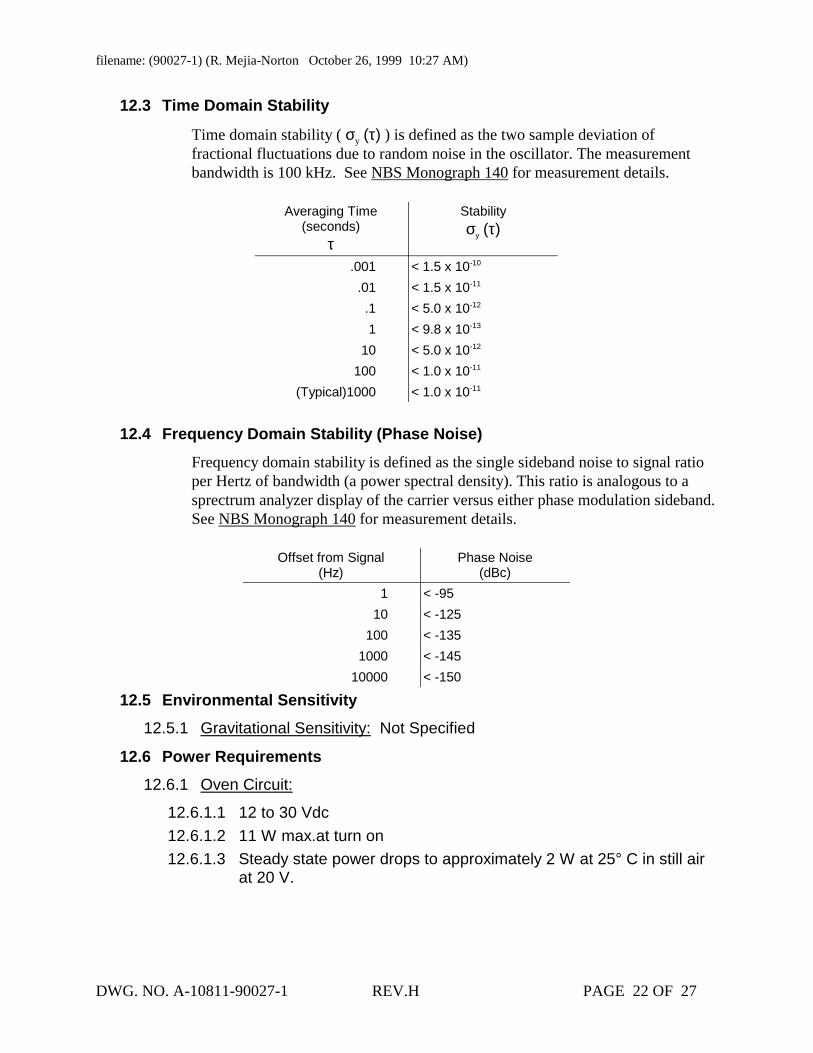
12.3 Time Domain Stability
Time domain stability ( σy (τ) ) is defined as the two sample deviation offractional fluctuations due to random noise in the oscillator. The measurementbandwidth is 100 kHz. See NBS Monograph 140 for measurement details.
Averaging Time(seconds)
τ
Stabilityσy (τ)
.001 < 1.5 x 10⁻¹⁰
.01 < 1.5 x 10⁻¹¹
.1 < 5.0 x 10⁻¹²
1 < 9.8 x 10⁻¹³
10 < 5.0 x 10⁻¹²
100 < 1.0 x 10⁻¹¹
(Typical)1000 < 1.0 x 10⁻¹¹
12.4 Frequency Domain Stability (Phase Noise)Frequency domain stability is defined as the single sideband noise to signal ratioper Hertz of bandwidth (a power spectral density). This ratio is analogous to asprectrum analyzer display of the carrier versus either phase modulation sideband.See NBS Monograph 140 for measurement details.
Offset from Signal(Hz)
Phase Noise(dBc)
1 < -95 10 < -125
100 < -135 1000 < -145
10000 < -150
12.5 Environmental Sensitivity12.5.1 Gravitational Sensitivity: Not Specified
12.6 Power Requirements12.6.1 Oven Circuit:
12.6.1.1 12 to 30 Vdc12.6.1.2 11 W max.at turn on12.6.1.3 Steady state power drops to approximately 2 W at 25° C in still air
at 20 V.
filename: (90027-1) (R. Mejia-Norton October 26, 1999 10:27 AM)
DWG. NO. A-10811-90027-1 REV.H PAGE 22 OF 27

13 10811-60160The performance specifications in section 13 also apply to the following optionsand subassemblies:
The performance specifications for the 10811-60160 are the same as the10811-60111 with the following exceptions:
13.1 Frequency Adjustment13.1.1 Coarse Tuning Range: > ± 5x10⁻⁷ (± 5 Hz).
13.1.2 Electronic Frequency Control (EFC): > ± 2.0x10⁻⁷ (± 2.5 Hz) for control.range of -5V to +5V
13.2 Power Requirements13.2.1 Oven Circuit:
13.2.1.1 12 to 30 Vdc13.2.1.2 11 W max.at turn on13.2.1.3 Steady state power drops to approximately 2 W at 25° C in still air
at 20 V.
filename: (90027-1) (R. Mejia-Norton October 26, 1999 10:27 AM)
DWG. NO. A-10811-90027-1 REV.H PAGE 23 OF 27

14 10811-60164The performance specifications in section 6 also apply to the followingsubassemblies:
The performance specifications for the 10811-60164 are the same as the10811D/E with the following exceptions:
14.1 Output Signal14.1.1 Harmonic Distortion: Not Specified
14.1.2 Spurious Phase Modulation: Not Specified
14.2 Frequency Adjustment14.2.1 Coarse Tuning Range: > ± 5x10⁻⁷ (± 5 Hz).
14.2.2 Electronic Frequency Control (EFC): > ± 2.0x10⁻⁷ (± 2.5 Hz) for control.range of -5V to +5V
14.3 Frequency Stability14.3.1 Long Term Stability (Aging Rate):
Aging rate (long term frequency stability is defined as the absolute value(magnitude) of the fractional frequency change with time. An observation timesufficiently long to reduce the effects of random noise to an insignificant value isimplied. Frequency changes due to environmental effects must be consideredseparately.
14.3.1.1 < 1 x 10⁻⁸ / day 14.4 Time Domain Stability
Not Specified14.5 Frequency Domain Stability (Phase Noise)
Not Specified.
filename: (90027-1) (R. Mejia-Norton October 26, 1999 10:27 AM)
DWG. NO. A-10811-90027-1 REV.H PAGE 24 OF 27

14.6 Warm UpNot Specified
14.7 Environmental SensitivityNot Specified
14.8 Power Requirements14.8.1 Oven Circuit:
14.8.1.1 12 to 30 Vdc14.8.1.2 11 W max.at turn on14.8.1.3 Steady state power drops to approximately 2 W at 25° C in still air
at 20 V.
filename: (90027-1) (R. Mejia-Norton October 26, 1999 10:27 AM)
DWG. NO. A-10811-90027-1 REV.H PAGE 25 OF 27

15 Index
Product/Assembly PCO SectionNumber Description Status Number Number05071-60219 5071A, SCD only 1105071-69219 05071-60219 "Blue Stripe" Exchange 1110811-60102 10811E #H40 & H41 subassembly Obsolete 2-24149 1010811-60109 5065A/5061B, SCD only 710811-60111 Counter products. SCD only 610811-60120 10811D Replacement 110811-60121 10811D #001 Replacement Obsolete 2-23915 210811-60122 10811D #002 Replacement Obsolete 2-23915 310811-60123 10811D #003 Replacement Obsolete 2-23915 410811-60125 10811D #100 Replacement Obsolete 2-21686 510811-60126 10811E Replacement 110811-60127 10811E #001 Replacement Obsolete 2-23915 210811-60128 10811E #002 Replacement Obsolete 2-23915 310811-60129 10811E #003 Replacement Obsolete 2-23915 410811-60131 10811E #100 Replacement Obsolete 2-21931 510811-60132 10811E #H40 Replacement Obsolete 2-24149 110811-60133 10811E #H41 Replacement Obsolete 2-22396 510811-60152 10811D #023 subassembly Obsolete 2-2193110811-60153 10811E #023 subassembly Obsolete 2-2193110811-60154 Untested 10811E subassembly10811-60155 Untested 10811D subassembly10811-60158 Sealed osc. with -60005 brd. set 1210811-60159 Sealed osc. with -60005 brd. set/studs 1210811-60160 "D" type osc. with -60005 brd. set 1310811-60164 Osc-159 Rdcd Spec 2-22774 1410811-60209 Spokane Div Only Obsolete 2-21931 810811-60211 Counter products, SCD only 910811-60260 Improved Aging 2-23023 910811-69001 10811-60111 "Blue Stripe" Exchange 610811-69120 10811D "Blue Stripe" Exchange 110811-69126 10811E "Blue Stripe" Replacement 110811-69132 10811E #H40 "Blue Stripe" Exchange Obsolete 2-24149 110811-69133 10811E #H41 "Blue Stripe" Exchange Obsolete 2-22396 510811D 110811D #001 Improved aging Obsolete 2-23915 210811D #002 Improved phase noise Obsolete 2-23915 3
filename: (90027-1) (R. Mejia-Norton October 26, 1999 10:27 AM)
DWG. NO. A-10811-90027-1 REV.H PAGE 26 OF 27

Product/Assembly PCO SectionNumber Description Status Number Number10811D #003 Improved aging and phase noise Obsolete 2-23915 410811D #023 10.23 MHz Obsolete 2-2167710811D #100 Reduced Spec Obsolete 2-21686 510811E 110811E #001 Improved aging Obsolete 2-23915 210811E #002 Improved phase noise Obsolete 2-23915 310811E #003 Improved aging and phase noise Obsolete 2-23915 410811D #023 10.23 MHz Obsolete 2-2167710811E #100 Reduced Spec Obsolete 2-21686 510811E #H40 Obsolete 2-24149 110811E #H41 Obsolete 2-22396 5
filename: (90027-1) (R. Mejia-Norton October 26, 1999 10:27 AM)
DWG. NO. A-10811-90027-1 REV.H PAGE 27 OF 27

Tel: (416) 754 - 3322Page 36
305/315/355 SERIES ORDERING CODEExample Part Number 305 - 056 - 521 - 2 04
SeriesTotal Number of ContactsContact CodeInsulator StyleMounting Options
FEATURES 305/355 Series CSA Approved and UL Recognized 315 Series UL Recognized .156 (3.96) Contact Spacing x .140 (3.56) Row Spacing Accepts .062 (1.57) Nominal Thickness P.C. Board Low Profile Insulator Body, .460 (11.68) Contact Termination Options include P.C. Tail, Wire Hole &
Extender Board Bends Large Variety of Mounting Options Pre-assembled Card Guides Available Accepts Between Contact and In-Contact Polarizing Keys
SPECIFICATIONS Insulator Material: Thermoplastic Polyester, UL 94V-0 Contact Material: Copper, Nickel, Tin Alloy CA-725 Contact Plating: Gold on the Mating Area, Tin on the
Contact Tails, Nickel Underplate Current Rating: 5 Amperes Continuous Contact Resistance: 10 Milliohms Maximum Dielectric Withstanding Voltage: 1800 V AC rms at Sea Level
Between Adjacent Contacts Insulation Resistance: 5000 Megohms Minimum Operating Temperature: -65 to +105 Degrees C Insertion Force: 16 oz (4.45 N) Maximum per Contact Pair
when Tested with a .070 (1.78) Thick Gauge Withdrawal Force: 1 oz (0.28 N) Minimum per Contact Pair
when Tested with a .054 (1.37) Thick Gauge
Series Insulator Colour Card Slot Length305 Green Standard Length per MIL-C-21097315 Green .020 (0.51) Shorter than Standard355 Black Standard Length per MIL-C-21097
Total Number of Contacts 1 Contact Rows012, 014,...086 Dual Row
Contact Code 2, 3 Description & Tail Size Tail Length "G"500 Wire Hole.087 x .013 (2.21 x 0.33) .282 (7.16)520 P.C. Tail .046 x .013 (1.17 x 0.33) .213 (5.41)521 P.C. Tail .046 x .013 (1.17 x 0.33) .125 (3.18)555 Extender Board Bend (Code 500 Contacts)556 Extender Board Bend (Code 520 Contacts)
Insulator Style 4 Description2 .295 (7.49) Card Slot Depth5 .330 (8.38) Card Slot Depth
Mounting Options 5 Description01 No Mounting Lugs02 .128 (3.25) Dia. Mounting Holes03 .116 (2.95) I.D. Floating Eyelets04 .156 (3.96) Dia. Mounting Holes07 M3-0.5 Metric Threaded Inserts08 #4-40 Unified Threaded Inserts58 .468 (11.89) Offset Card Guides68 .344 (8.74) Offset Card Guides78 In-Line Card Guides
Ordering Code Notes1) All connector sizes up to 86 contacts dual row are available
upon request.2) Consult with Edac regarding single row configuration and
wire wrap tail options.3) For details of the extender board bends, refer to page 66.4) Insulator style code 5 is available for the 305 and 355 series
upon request.5) For details of the mounting options, refer to page 68.
305/315/355 SERIES CARD EDGE CONNECTOR.156" (3.96mm) Contact Spacing

Fax: (416) 754 -3299 Page 37
CARD EDGE CONNECTOR SERIES 305/315/355Contact Spacing .156" (3.96mm)
NUMBER OF "A" "B" "C" "D" "E"CONTACTS 305, 355 315
Dual Inch (mm) Inch (mm) Inch (mm) Inch (mm) Inch (mm) Inch (mm)
12 1.842 (46.79) 1.532 (38.91) 1.246 (31.65) 1.100 (27.94) 1.080 (27.43) .780 (19.81)
20 2.466 (62.64) 2.156 (54.76) 1.870 (47.50) 1.724 (43.79) 1.704 (43.28) 1.404 (35.66)
24 2.778 (70.56) 2.468 (62.69) 2.182 (55.42) 2.036 (51.71) 2.016 (51.21) 1.716 (43.59)
30 3.246 (82.45) 2.936 (74.57) 2.650 (67.31) 2.504 (63.60) 2.484 (63.09) 2.184 (55.47)
36 3.714 (94.34) 3.404 (86.46) 3.118 (79.20) 2.972 (75.49) 2.952 (74.98) 2.652 (67.36)
44 4.338 (110.19) 4.028 (102.31) 3.742 (95.05) 3.596 (91.34) 3.576 (90.83) 3.276 (83.21)
48 4.650 (118.11) 4.340 (110.24) 4.054 (102.97) 3.908 (99.26) 3.888 (98.76) 3.588 (91.14)
50 4.806 (122.07) 4.496 (114.20) 4.210 (106.93) 4.064 (103.23) 4.044 (102.72) 3.744 (95.10)
56 5.274 (133.96) 4.964 (126.09) 4.678 (118.82) 4.532 (115.11) 4.512 (114.60) 4.212 (106.98)
60 5.586 (141.88) 5.276 (134.01) 4.990 (126.75) 4.844 (123.04) 4.824 (122.53) 4.524 (114.91)
72 6.522 (165.66) 6.212 (157.78) 5.926 (150.52) 5.780 (146.81) 5.760 (146.30) 5.460 (138.68)
86 7.614 (193.40) 7.304 (185.52) 7.018 (178.26) 6.872 (174.55) 6.852 (174.04) 6.552 (166.42)
Dimensions of Other Connector Sizes are Listed on Page 74

Tel: (416) 754 - 3322Page 74
.156" (3.96mm) CONTACT SPACING CONNECTOR DIMENSIONS303, 305, 306, 307, 315, 316, 317, 333, 336, 337, 355, 356, 357, 387, 737 Series Card Edge Connectors
DIMENSION "A" "B"REST OF REST OF
SERIES 317 333 336 SERIES 317 333, 336 SERIES
Number ofContacts
Single Dual Inch (mm) Inch (mm) Inch (mm) Inch (mm) Inch (mm) Inch (mm) Inch (mm)
6 12 1.830 (46.48) 1.784 (45.31) 1.857 (47.17) 1.842 (46.79) 1.539 (39.09) 1.534 (38.96) 1.532 (38.91)
7 14 1.986 (50.44) 1.940 (49.28) 2.013 (51.13) 1.998 (50.75) 1.695 (43.05) 1.690 (42.93) 1.688 (42.88)
8 16 2.142 (54.41) 2.096 (53.24) 2.169 (55.09) 2.154 (54.71) 1.851 (47.02) 1.846 (46.89) 1.844 (46.84)
9 18 2.298 (58.37) 2.252 (57.20) 2.325 (59.06) 2.310 (58.67) 2.007 (50.98) 2.002 (50.85) 2.000 (50.80)
10 20 2.454 (62.33) 2.408 (61.16) 2.481 (63.02) 2.466 (62.64) 2.163 (54.94) 2.158 (54.81) 2.156 (54.76)
11 22 2.610 (66.29) 2.564 (65.13) 2.637 (66.98) 2.622 (66.60) 2.319 (58.90) 2.314 (58.78) 2.312 (58.72)
12 24 2.766 (70.26) 2.720 (69.09) 2.793 (70.94) 2.778 (70.56) 2.475 (62.87) 2.470 (62.74) 2.468 (62.69)
13 26 2.922 (74.22) 2.876 (73.05) 2.949 (74.90) 2.934 (74.52) 2.631 (66.83) 2.626 (66.70) 2.624 (66.65)
14 28 3.078 (78.18) 3.032 (77.01) 3.105 (78.87) 3.090 (78.49) 2.787 (70.79) 2.782 (70.66) 2.780 (70.61)
15 30 3.234 (82.14) 3.188 (80.98) 3.261 (82.83) 3.246 (82.45) 2.943 (74.75) 2.938 (74.63) 2.936 (74.57)
16 32 3.390 (86.11) 3.344 (84.94) 3.417 (86.79) 3.402 (86.41) 3.099 (78.71) 3.094 (78.59) 3.092 (78.54)
17 34 3.546 (90.07) 3.500 (88.90) 3.573 (90.75) 3.558 (90.37) 3.255 (82.68) 3.250 (82.55) 3.248 (82.50)
18 36 3.702 (94.03) 3.656 (92.86) 3.729 (94.72) 3.714 (94.34) 3.411 (86.64) 3.406 (86.51) 3.404 (86.46)
19 38 3.858 (97.99) 3.812 (96.82) 3.885 (98.68) 3.870 (98.30) 3.567 (90.60) 3.562 (90.47) 3.560 (90.42)
20 40 4.014 (101.96) 3.968 (100.79) 4.041 (102.64) 4.026 (102.26) 3.723 (94.56) 3.718 (94.44) 3.716 (94.39)
21 42 4.170 (105.92) 4.124 (104.75) 4.197 (106.60) 4.182 (106.22) 3.879 (98.53) 3.874 (98.40) 3.872 (98.35)
22 44 4.326 (109.88) 4.280 (108.71) 4.353 (110.57) 4.338 (110.19) 4.035 (102.49) 4.030 (102.36) 4.028 (102.31)
23 46 4.482 (113.84) 4.436 (112.67) 4.509 (114.53) 4.494 (114.15) 4.191 (106.45) 4.186 (106.32) 4.184 (106.27)
24 48 4.638 (117.81) 4.592 (116.64) 4.665 (118.49) 4.650 (118.11) 4.347 (110.41) 4.342 (110.29) 4.340 (110.24)
25 50 4.794 (121.77) 4.748 (120.60) 4.821 (122.45) 4.806 (122.07) 4.503 (114.38) 4.498 (114.25) 4.496 (114.20)
26 52 4.950 (125.73) 4.904 (124.56) 4.977 (126.42) 4.962 (126.03) 4.659 (118.34) 4.654 (118.21) 4.652 (118.16)
27 54 5.106 (129.69) 5.060 (128.52) 5.133 (130.38) 5.118 (130.00) 4.815 (122.30) 4.810 (122.17) 4.808 (122.12)
28 56 5.262 (133.65) 5.216 (132.49) 5.289 (134.34) 5.274 (133.96) 4.971 (126.26) 4.966 (126.14) 4.964 (126.09)
29 58 5.418 (137.62) 5.372 (136.45) 5.445 (138.30) 5.430 (137.92) 5.127 (130.23) 5.122 (130.10) 5.120 (130.05)
30 60 5.574 (141.58) 5.528 (140.41) 5.601 (142.27) 5.586 (141.88) 5.283 (134.19) 5.278 (134.06) 5.276 (134.01)
31 62 5.730 (145.54) 5.684 (144.37) 5.757 (146.23) 5.742 (145.85) 5.439 (138.15) 5.434 (138.02) 5.432 (137.97)
32 64 5.886 (149.50) 5.840 (148.34) 5.913 (150.19) 5.898 (149.81) 5.595 (142.11) 5.590 (141.99) 5.588 (141.94)
33 66 6.042 (153.47) 5.996 (152.30) 6.069 (154.15) 6.054 (153.77) 5.751 (146.08) 5.746 (145.95) 5.744 (145.90)
34 68 6.198 (157.43) 6.152 (156.26) 6.225 (158.12) 6.210 (157.73) 5.907 (150.04) 5.902 (149.91) 5.900 (149.86)
35 70 6.354 (161.39) 6.308 (160.22) 6.381 (162.08) 6.366 (161.70) 6.063 (154.00) 6.058 (153.87) 6.056 (153.82)
36 72 6.510 (165.35) 6.464 (164.19) 6.537 (166.04) 6.522 (165.66) 6.219 (157.96) 6.214 (157.84) 6.212 (157.78)
37 74 6.666 (169.32) 6.620 (168.15) 6.693 (170.00) 6.678 (169.62) 6.375 (161.93) 6.370 (161.80) 6.368 (161.75)
38 76 6.822 (173.28) 6.776 (172.11) 6.849 (173.96) 6.834 (173.58) 6.531 (165.89) 6.526 (165.76) 6.524 (165.71)
39 78 6.978 (177.24) 6.932 (176.07) 7.005 (177.93) 6.990 (177.55) 6.687 (169.85) 6.682 (169.72) 6.680 (169.67)
40 80 7.134 (181.20) 7.088 (180.04) 7.161 (181.89) 7.146 (181.51) 6.843 (173.81) 6.838 (173.69) 6.836 (173.63)
41 82 7.290 (185.17) 7.244 (184.00) 7.317 (185.85) 7.302 (185.47) 6.999 (177.77) 6.994 (177.65) 6.992 (177.60)
42 84 7.446 (189.13) 7.400 (187.96) 7.473 (189.81) 7.458 (189.43) 7.155 (181.74) 7.150 (181.61) 7.148 (181.56)
43 86 7.602 (193.09) 7.556 (191.92) 7.629 (193.78) 7.614 (193.40) 7.311 (185.70) 7.306 (185.57) 7.304 (185.52)
44 88 7.770 (197.36) 7.460 (189.48)

Fax: (416) 754 -3299 Page 75
CONNECTOR DIMENSIONS CONTACT SPACING .156" (3.96mm)Card Edge Connector Series 303, 305, 306, 307, 315, 316, 317, 333, 336, 337, 355, 356, 357, 387, 737
DIMENSION "C" "D" "E"REST OF REST OF ALL
SERIES 303, 317 333 336 SERIES 315, 316 SERIES SERIES
Number ofContacts
Single Dual Inch (mm) Inch (mm) Inch (mm) Inch (mm) Inch (mm) Inch (mm) Inch (mm)
6 12 1.220 (30.99) 1.261 (32.03) 1.216 (30.89) 1.246 (31.65) 1.080 (27.43) 1.100 (27.94) .780 (19.81)
7 14 1.376 (34.95) 1.417 (35.99) 1.372 (34.85) 1.402 (35.61) 1.236 (31.39) 1.256 (31.90) .936 (23.77)
8 16 1.532 (38.91) 1.573 (39.95) 1.528 (38.81) 1.558 (39.57) 1.392 (35.36) 1.412 (35.86) 1.092 (27.74)
9 18 1.688 (42.88) 1.729 (43.92) 1.684 (42.77) 1.714 (43.54) 1.548 (39.32) 1.568 (39.83) 1.248 (31.70)
10 20 1.844 (46.84) 1.885 (47.88) 1.840 (46.74) 1.870 (47.50) 1.704 (43.28) 1.724 (43.79) 1.404 (35.66)
11 22 2.000 (50.80) 2.041 (51.84) 1.996 (50.70) 2.026 (51.46) 1.860 (47.24) 1.880 (47.75) 1.560 (39.62)
12 24 2.156 (54.76) 2.197 (55.80) 2.152 (54.66) 2.182 (55.42) 2.016 (51.21) 2.036 (51.71) 1.716 (43.59)
13 26 2.312 (58.72) 2.353 (59.77) 2.308 (58.62) 2.338 (59.39) 2.172 (55.17) 2.192 (55.68) 1.872 (47.55)
14 28 2.468 (62.69) 2.509 (63.73) 2.464 (62.59) 2.494 (63.35) 2.328 (59.13) 2.348 (59.64) 2.028 (51.51)
15 30 2.624 (66.65) 2.665 (67.69) 2.620 (66.55) 2.650 (67.31) 2.484 (63.09) 2.504 (63.60) 2.184 (55.47)
16 32 2.780 (70.61) 2.821 (71.65) 2.776 (70.51) 2.806 (71.27) 2.640 (67.06) 2.660 (67.56) 2.340 (59.44)
17 34 2.936 (74.57) 2.977 (75.62) 2.932 (74.47) 2.962 (75.23) 2.796 (71.02) 2.816 (71.53) 2.496 (63.40)
18 36 3.092 (78.54) 3.133 (79.58) 3.088 (78.44) 3.118 (79.20) 2.952 (74.98) 2.972 (75.49) 2.652 (67.36)
19 38 3.248 (82.50) 3.289 (83.54) 3.244 (82.40) 3.274 (83.16) 3.108 (78.94) 3.128 (79.45) 2.808 (71.32)
20 40 3.404 (86.46) 3.445 (87.50) 3.400 (86.36) 3.430 (87.12) 3.264 (82.91) 3.284 (83.41) 2.964 (75.29)
21 42 3.560 (90.42) 3.601 (91.47) 3.556 (90.32) 3.586 (91.08) 3.420 (86.87) 3.440 (87.38) 3.120 (79.25)
22 44 3.716 (94.39) 3.757 (95.43) 3.712 (94.28) 3.742 (95.05) 3.576 (90.83) 3.596 (91.34) 3.276 (83.21)
23 46 3.872 (98.35) 3.913 (99.39) 3.868 (98.25) 3.898 (99.01) 3.732 (94.79) 3.752 (95.30) 3.432 (87.17)
24 48 4.028 (102.31) 4.069 (103.35) 4.024 (102.21) 4.054 (102.97) 3.888 (98.76) 3.908 (99.26) 3.588 (91.14)
25 50 4.184 (106.27) 4.225 (107.32) 4.180 (106.17) 4.210 (106.93) 4.044 (102.72) 4.064 (103.23) 3.744 (95.10)
26 52 4.340 (110.24) 4.381 (111.28) 4.336 (110.13) 4.366 (110.90) 4.200 (106.68) 4.220 (107.19) 3.900 (99.06)
27 54 4.496 (114.20) 4.537 (115.24) 4.492 (114.10) 4.522 (114.86) 4.356 (110.64) 4.376 (111.15) 4.056 (103.02)
28 56 4.652 (118.16) 4.693 (119.20) 4.648 (118.06) 4.678 (118.82) 4.512 (114.60) 4.532 (115.11) 4.212 (106.98)
29 58 4.808 (122.12) 4.849 (123.16) 4.804 (122.02) 4.834 (122.78) 4.668 (118.57) 4.688 (119.08) 4.368 (110.95)
30 60 4.964 (126.09) 5.005 (127.13) 4.960 (125.98) 4.990 (126.75) 4.824 (122.53) 4.844 (123.04) 4.524 (114.91)
31 62 5.120 (130.05) 5.161 (131.09) 5.116 (129.95) 5.146 (130.71) 4.980 (126.49) 5.000 (127.00) 4.680 (118.87)
32 64 5.276 (134.01) 5.317 (135.05) 5.272 (133.91) 5.302 (134.67) 5.136 (130.45) 5.156 (130.96) 4.836 (122.83)
33 66 5.432 (137.97) 5.473 (139.01) 5.428 (137.87) 5.458 (138.63) 5.292 (134.42) 5.312 (134.92) 4.992 (126.80)
34 68 5.588 (141.94) 5.629 (142.98) 5.584 (141.83) 5.614 (142.60) 5.448 (138.38) 5.468 (138.89) 5.148 (130.76)
35 70 5.744 (145.90) 5.785 (146.94) 5.740 (145.80) 5.770 (146.56) 5.604 (142.34) 5.624 (142.85) 5.304 (134.72)
36 72 5.900 (149.86) 5.941 (150.90) 5.896 (149.76) 5.926 (150.52) 5.760 (146.30) 5.780 (146.81) 5.460 (138.68)
37 74 6.056 (153.82) 6.097 (154.86) 6.052 (153.72) 6.082 (154.48) 5.916 (150.27) 5.936 (150.77) 5.616 (142.65)
38 76 6.212 (157.78) 6.253 (158.83) 6.208 (157.68) 6.238 (158.45) 6.072 (154.23) 6.092 (154.74) 5.772 (146.61)
39 78 6.368 (161.75) 6.409 (162.79) 6.364 (161.65) 6.394 (162.41) 6.228 (158.19) 6.248 (158.70) 5.928 (150.57)
40 80 6.524 (165.71) 6.565 (166.75) 6.520 (165.61) 6.550 (166.37) 6.384 (162.15) 6.404 (162.66) 6.084 (154.53)
41 82 6.680 (169.67) 6.721 (170.71) 6.676 (169.57) 6.706 (170.33) 6.540 (166.12) 6.560 (166.62) 6.240 (158.50)
42 84 6.836 (173.63) 6.877 (174.68) 6.832 (173.53) 6.862 (174.29) 6.696 (170.08) 6.716 (170.59) 6.396 (162.46)
43 86 6.992 (177.60) 7.033 (178.64) 6.988 (177.50) 7.018 (178.26) 6.852 (174.04) 6.872 (174.55) 6.552 (166.42)
44 88 7.174 (182.22) 7.028 (178.51) 6.708 (170.38)

Tel: (416) 754 - 3322Page 68
MOUNTING OPTIONS - CARD EDGE CONNECTORSStandard Mounting Details
CODE x01 - NO MOUNTING LUGS Applicable for 303, 305, 306, 307, 310, 315, 316, 317, 321, 325, 327, 333, 336, 337, 338,
340, 341, 342, 345, 346, 355, 356, 357, 379, 384, 387, 391, 392, 395 and 396 Series
CODE x02, x04 & x09 - THROUGH MOUNTING HOLESApplicable Series Code x02 Code x04 Code x09
"A" Dia. "A" Dia. "A" Dia.303, 305, 306, 307, 310, 315, .128 (3.25) .156 (3.96) —316,321, 333, 337, 338, 340,341, 345,346, 355, 356, 357,379, 384, 387,391, 395, 396317, 323 .144 (3.66) .156 (3.96) —325 — — .160 (4.06)327 — — .163 (4.14)336 .128 (3.25) .156 (3.96) .178 (4.52)342, 392 .128(3.25) x .156 (3.96) —
.146 (3.71)Slot
CODE x03 - FLOATING EYELETSApplicable Series "A"303, 305, 306, 307, 310, 315, 316, .328 (8.33)317, 321, 323, 333, 336, 337, 338,341, 345, 346, 355, 356, 357, 379,384, 387, 391, 395, 396342, 392 .348 (8.84)
CODE x07 & x08 - THREADED INSERTS Applicable for 303, 305, 306, 307, 310, 315, 316, 317, 321, 323, 325, 333, 336, 337, 338,
341, 342, 345, 346, 356, 357, 379, 384, 387, 391, 392, 395 and 396 Series See Code x12 for Side Mounting Threaded Inserts
CODE x12 - SIDE MOUNTING HOLESApplicable Series "A"307, 333, 337, 345, 346, 357, 387, .125 (3.18)395, 396342, 392 .135 (3.43)
Series Listed Above based on Availability of 90 Degree Bend Contact Tails.Side Mounting Holes may also be Used for Other Card Edge Connectors with aLug Height of .250 (6.35) or Greater.
For Side Mounting with Threaded Inserts, Specify Code x17 for M3-0.5 MetricThreads or Code x18 for #4-40 Unified Threads.

Fax: (416) 754 -3299 Page 69
CODE x58 & x68 - OFFSET CARD GUIDESApplicable Series for "A" "B" "C" "D"Code x58 Guides305, 306, 307, 315, .468(11.89) 2.755(69.98) .125 (3.18) .423(10.74)316, 337, 338, 355,356, 357, 387345, 395 .468(11.89) 2.755(69.98) .120 (3.05) .402(10.21)346, 396 .468(11.89) 2.755(69.98) .120 (3.05) .398(10.11)
Applicable Series for "A" "B" "C" "D"Code x68 Guides305, 306, 307, 315, .344 (8.74) 2.505(63.63) .060 (1.52) .242 (6.15)316, 337, 338, 355,356, 357, 387
For Card Guides with .128 (3.25) Dia. Through Hole Inserts, Specify Code x52 or x62. For Card Guides with M3-0.5 Metric Threaded Inserts, Specify Code x57 or x67. For Field Assembly of Card Guides, Refer to Page 71.
CARD EDGE CONNECTORS - MOUNTING OPTIONSStandard Mounting Details
CODE x78 & x88 - IN-LINE CARD GUIDESApplicable Series for "B" "C"Code x78 Guides305, 306, 307, 315, 316, 337, 338, 1.550(39.37) .090 (2.29)355, 356, 357, 387317 1.712(43.48) .110 (2.79)345, 395 2.750(69.85) .083 (2.11)346, 396 2.750(69.85) .091 (2.31)
Applicable Series for "B" "C"Code x88 Guides345, 395 1.250(31.75) .083 (2.11)
In-Line Card Guides are Not Suitable for the Flush Mounting Lug Versions of 337,387, 346 or 396 Series
For Card Guides with .128 (3.25) Dia. Through Hole Inserts, Specify Code x72 or x82. For Card Guides with M3-0.5 Metric Threaded Inserts, Specify Code x77 or x87 For Field Assembly of Card Guides, Refer to Page 71.
www.vishay.com14
EB8Vishay Dale
Document Number 36005Revision 14-Aug-02
For technical questions, contact [email protected]
Edgeboard Connectors, Dual ReadoutFEATURES• 0.156" C-C x 0.200" grid [3.96mm x 5.08mm].• Greater design latitude.
3 body materials: Diallyl phthalate, phenolic and glass-filled polyester.6 contact termination styles.8 body sizes.7 mounting styles.
• Bifurcated bellows contacts provide 2 flexing contactsurfaces to assure positive contact.
• Accepts PC board thickness of 0.054" - 0.071"[1.37mm -1.80mm].
• Polarization between contact positions in all sizes.• Selective gold plating.• Recognized under the Component Program of
Underwriters Laboratories, Inc. Listed under FileE65524, Project 77CH3889.
ELECTRICAL SPECIFICATIONSCurrent Rating: 5 amps.
Test Voltage Between Contacts:At sea level: 1800VRMS.
At 70,000 feet [21,336 meters]: 450VRMS.
Insulation Resistance: 5000 Megohm minimum at500VDC potential.
Contact Resistance: 30 millivolts maximum at ratedcurrent (with gold plating).
Operating Temperature: - 55°C to + 125°C.
Humidity: 96 hours at 90% relative humidity at + 40°C,dried at room temperature for 3 hours minimum, insulationresistance 5000 Megohm.
Durability: (With gold plating.) After 500 cycles of insertionand withdrawal of 0.070" [1.78mm] thick steel test gauge,contact resistance less than 0.030V at 5 amps and individualcontact retention force when measured with a 0.054" [1.37mm]thick steel test pin greater than 1/2 ounce.
Shock: Three 50g shocks in each of 3 mutually perpendicularplanes with no loss of continuity.
Vibration: 2 hours in each of 3 mutually perpendicular planes,frequency sweep 10 to 55cps at 0.06 double amplitude withno loss of continuity.
APPLICATIONSFor use with 0.062" [1.57mm] printed circuit boards requiringan edgeboard type connector on .156" [3.96mm] centers.PHYSICAL SPECIFICATIONSContact Type: Bifurcated bellows.Number of Contacts: 6, 10, 12, 15, 18, 22, 24, 25 per side.Contact Spacing: 0.156" [3.96mm] center to center.Card Thickness: 0.054" to 0.071" [1.37mm to 1.80mm].Card Slot Depth: 0.330" [8.38mm], dual readout.
MATERIAL SPECIFICATIONSBody:“1” glass-filled diallyl phthalate per MIL-M-14, Type SDG-Fgreen, flame retardant (UL 94V-0).“2” glass-filled phenolic per MIL-M-14, Type MFH dark green,flame retardant (UL 94V-0).“3” thermoplastic polyester, glass-filled, black, flameretardant (UL 94V-0).“5” thermoplastic polyphenylene sulfied, glass-filled, brown,flame retardant (UL 94V-0).Contacts: Phosphor bronze.Polarizing Key: Glass reinforced nylon, flame retardant(UL 94V-O).Contact Plating: Gold (See Ordering Information).
NOTE: High temperature burn-in, edgeboard connectors,0.156" [3.96mm] center to center are on page 20 of this catalog.
SG = Selective Gold Plating(0.00003" [0.000762mm]minimum thick) on contactarea with Gold Flash onterminal.SGF = Selective Gold Plating(0.00001" [0.000254mm]minimum thick) on contactarea with Gold Flash onterminal.All Gold Plating over 0.00005"[0.00127mm] minimum NickelUnderplate.Contact factory for additionalplating options.
Key(s) arelocated toright ofpos i t ion(s)designated.R e q u i r e donly whenp o l a r i z i n gkeys are tobe factoryinstalled.
ORDERING INFORMATIONEB8
MODEL1
BODY MATERIAL
Optional BodyMaterial
1 = DiallylPhthalate
2 = Phenolic3 = Glass-filled
Polyester5 = Glass-filled
PolyphenyleneSulfied
BOPTIONALCONTACTS
A, C, D,K, L or E
ASTANDARDTERMINAL
VARIATIONS
22CONTACTS
6, 10, 12,15, 18, 22,24 or 25
SGCONTACTPLATING
XMOUNTINGVARIATIONS
APOLARIZING
KEYPOSITIONS
Beryllium Coppercontacts optional.Available in “A” and“E” contact stylesonly. (Omit forstandard.)

www.vishay.com15
EB8Vishay Dale
Document Number 36005Revision 14-Aug-02
For technical questions, contact [email protected]
DIMENSIONS in inches [millimeters]
TERMINAL VARIATIONS in inches [millimeters]
Type “A”Pierced
Type “C” Type “D”Solder Dip
Type “L”SolderDip
Section C-C
# OF CONTACTPOSITIONS A B D E
6 1.78 [45.21] 1.531 [38.89] 1.240 [31.50] 1.100 [27.94]
10 2.41 [61.21] 2.156 [54.76] 1.864 [47.35] 1.724 [43.79]
12 2.72 [69.09] 2.469 [62.71] 2.176 [55.27] 2.036 [51.71]
15 3.19 [81.03] 2.937 [74.60] 2.644 [67.16] 2.504 [63.60]
18 3.66 [92.96] 3.406 [86.51] 3.112 [79.05] 2.972 [75.49]
22 4.28 [108.71] 4.031 [102.39] 3.736 [94.89] 3.596 [91.34]
24 4.59 [116.59] 4.344 [110.33] 4.051 [102.89] 3.911 [99.34]
25 4.75 [120.65] 4.500 [114.30] 4.207 [106.86] 4.067 [103.30]
Type “K”Solder Dip
0.054 - 0.071[1.37 - 1.80]
0.200[5.08]
0.330 [8.38]Depth of
CardInsertion
0.030 [.762]
0.350 [8.89]Typ.
0.156 [3.96]Typ.
See Table forContact Variations
0.250[6.35]
0.460[11.70]
0.060 [1.52] R Typ.
CC
A
B
E
D
0.340 [8.64]
0.200 ± 0.015 [5.08 ± 0.381]
To fit 3,#22 AWG Wires
0.086 [2.18]
0.200 ± 0.015 [5.08 ± 0.381]
0.125 ± 0.015 [3.18 ± 0.381]
To fit 0.051 [1.30]Dia. Eyelet
0.200 ± 0.015 [5.08 ± 0.381]
0.104 ± 0.015 [2.64 ± 0.381]
To fit 0.051[1.30]Dia. Eyelet
0.200 ± 0.015 [5.08 ± 0.381]
0.200 ± 0.015 [5.08 ± 0.381]
To fit 0.051[1.30]Dia. Eyelet
0.200 ± 0.015 [5.08 ± .381]
0.156 ± 0.015 [3.96 ± 0.381]
To fit 0.036 [0.914]Dia. Eyelet
Edgeboard Connectors, Dual Readout

www.vishay.com16
EB8Vishay Dale
Document Number 36005Revision 14-Aug-02
For technical questions, contact [email protected]
Type “E”Card Extender
When ordering polarizing keysindividually, specify Model Number:PK-8 between contacts.Hand insertion tool, TPK-8, provided onrequest.
TERMINAL VARIATIONS in inches [millimeters] POLARIZING KEY
0.120[3.05]
.325[8.26]
0.023[.584]
0.200 ± 0.015 [5.08 ± .381]
0.050[1.27]
15°Typ.
0.100[2.54]
120°Typ.
UsesType “A”Contact
0.086[2.18]
Type “V”Clearance Hole
Type “VI”Clearance Hole
No Mounting Pad
Type “XI”Clearance Hole
No Mounting Pad
Type “Y”Threaded Insert
Type “Z”Floating Bushing Radial Float 0.047 [1.19]
Type “X”Clearance Hole
Type “W”No Mounting Flange
MOUNTING VARIATIONS in inches [millimeters]
NOTE: Overall body lengthincreased by 0.060 [1.52].
0.142 [3.61] Dia.
0.250 [6.35]Ref.
0.128 [3.25]Dia.
0.220 [5.59]Ref.
4-40UNC-2B 0.250 [6.35]
Ref.
0.250 [6.35]Ref.
0.220 [5.59]Ref.
0.142[3.61]Dia.
0.010 [0.254]0.000 [0.000]
0.250 [6.35]Ref.
0.128 [3.25] Dia.
0.250 [6.35]Ref.
0.116[2.95]Dia.
0.250 [6.35]Dia.
0.270 [6.86]
Edgeboard Connectors, Dual Readout

Legal Disclaimer NoticeVishay
Document Number: 91000 www.vishay.comRevision: 08-Apr-05 1
Notice
Specifications of the products displayed herein are subject to change without notice. Vishay Intertechnology, Inc.,or anyone on its behalf, assumes no responsibility or liability for any errors or inaccuracies.
Information contained herein is intended to provide a product description only. No license, express or implied, byestoppel or otherwise, to any intellectual property rights is granted by this document. Except as provided in Vishay'sterms and conditions of sale for such products, Vishay assumes no liability whatsoever, and disclaims any expressor implied warranty, relating to sale and/or use of Vishay products including liability or warranties relating to fitnessfor a particular purpose, merchantability, or infringement of any patent, copyright, or other intellectual property right.
The products shown herein are not designed for use in medical, life-saving, or life-sustaining applications.Customers using or selling these products for use in such applications do so at their own risk and agree to fullyindemnify Vishay for any damages resulting from such improper use or sale.

fdrive.com.au253
GROMMETS
J3112 SERIES
Maximum Support Member
Part Number Figure Elastomer Axial Load Deflection Axial Spring Rate Radial Spring Rate Thickness Diameter
lbs N in mm lbs/in N/mm lbs/in N/mm in mm in mm
J311251 1a Natural 1 4 0.045 1.2 22 3.9 44 7.7 0.062 1.6 0.555 14.1
J3112611 1d Natural 1 4 0.045 1.1 22 3.9 44 7.7 0.062 1.6 0.555 14.1
J311222 1b Neoprene 2 9 0.060 1.5 33 5.8 66 11.6 0.062 1.6 0.555 14.1
J3112802 1c SPE 2 9 0.035 0.9 57 10.0 114 20.1 0.062 1.6 0.555 14.1
J311283 1c Neoprene 3 13 0.060 1.5 50 8.8 100 17.5 0.062 1.6 0.555 14.1
J3112804 1c SPE 4 18 0.035 0.9 114 20.1 228 40.2 0.062 1.6 0.555 14.1
J17736 SERIES
Maximum Support MemberPart Number Figure Elastomer Axial Load Deflection Axial Spring Rate Radial Spring Rate Thickness Diameter
lbs N in mm lbs/in N/mm lbs/in N/mm in mm in mm
J177362 2c Neoprene 1 4 0.060 1.5 17 2.6 17 2.6 0.062 1.6 0.555 14.1
J1773641 2c SPE 1 4 0.060 1.5 17 2.6 34 5.3 0.062 1.6 0.555 14.1
J2924 / J2927 SERIES
Maximum Support Member
Part Number Figure Elastomer Axial Load Deflection Axial Spring Rate Radial Spring Rate Thickness Diameter
J292421 3a 1 4 0.006 1.5 17 2.6 17 2.6 0.062 1.6 0.735 18.7
J2927461 3c Neoprene 1 4 0.060 1.5 17 2.6 17 2.6 0.062 1.6 0.735 18.7
J292714 3b Neoprene 4 18 0.060 1.5 65 11.4 65 11.4 0.062 1.6 0.735 18.7
344/L50