1 encoding logic for 5 bit analog to digital converter by:kaneez fatimah ranjini bhagavan padmavathy...
Post on 19-Dec-2015
214 views
TRANSCRIPT

1
Encoding Logic for 5 bit Analog to Digital Converter
By:Kaneez FatimahRanjini Bhagavan
Padmavathy DesikachariVeena Jain
Advisor: Dr. David ParentDate: 05/17/2004

2
Agenda
• Abstract• Introduction
- Why this Project - ADC Encoding Logic
• Project Details• Results• Cost Analysis• Summary

3
Abstract
• Designed Encoding logic for 5 bit Analog to Digital Converter without Sample and Hold operation
• Used AMI06 process
• Clock frequency = 200 MHz
• Power ~ 3mW@200MHz

4
Why this Project
• This project is based on IEEE Research paper on enhanced ADC logic without sample & hold
• Needed interpolation from basic 8 bit circuit to 5 bit logic
• Dr. Parent suggested to implement this idea

5
Encoding Logic• The design of converter is optimized to minimize the
effect of errors that may occur in ADC architecture without a sample & hold
• Two levels of Encoding
• Total Comparators # 32• First Encoding Level for n = 1 to 8 is given by
B[n] = {C[n] and (Not C[n+8])} OR {C[n+16] and (Not C[n+24])}
B[9] = {C[16] and (Not C[32])}OR {C[17] and (Not C[32])}
ComparatorsFirst
Encoding Level
Second Encoding
Level
CM1
CM32
B1
B9
Bit0
Bit1
Bit4

6
Encoding Logic Contd..
• Second Level of Encoding –
• Bit 0 = (B1 XOR B2) OR (B3 XOR B4) OR
(B5 XOR B6) OR (B7 XOR B8)
• Bit 1 = (B2 XOR B4) OR (B6 XOR B8)
• Bit 2 = (B4 XOR B8)
• Bit 3 = B8
• Bit4 = B9

7
Project Details
• Comparator output Simulated
• First Level Encoding
- Inverter, AOI22
• Second Level Encoding
- 2 input XOR, 2input OR , 4input OR
• Flipflop

8
Schematic

9
Verilog Simulation

10
Longest Path Calculations
Basic Block
Logic Level
Logic Gate
Cg to drive
#Cdn #Cdp #Ln #Lp Wn Wp Cg
Flipflop
1 NOR 30ff 2 3 Ln 2Lp 2.87u 5.07u 30ff
2 KeeperMUX
3 3 2Ln 2Lp 1.5u 1.5u
3 Driving MUX
3 3 2Ln 2Lp 2.87u 5.07u
4 INV 1 1 Ln Lp 2.87u 5.07u
OR 5 INV 30ff 1 1 Ln Lp 1.5u 2.48u 30ff
6 NOR 6.8 ff 7 7 4Ln Lp 1.5u 5.09u 11.26ff
XOR 7 AOI22 11.26ff
6 6 2Ln 2Lp 3.3u 5.5u 6.78ff
8 INV 6.78ff 1 1 Ln Lp 3.3 5.5u 6.78ff
AOI22 9 INV 26.8ff 1 1 Ln Lp 1.5u 2.53u 6.88ff
10 AOI22 6.88ff 6 6 2Ln 2Lp 1.5u 2.53u 6.88ff
INV 11 INV 6.88ff 1 1 Ln Lp 1.5u 2.53u
11
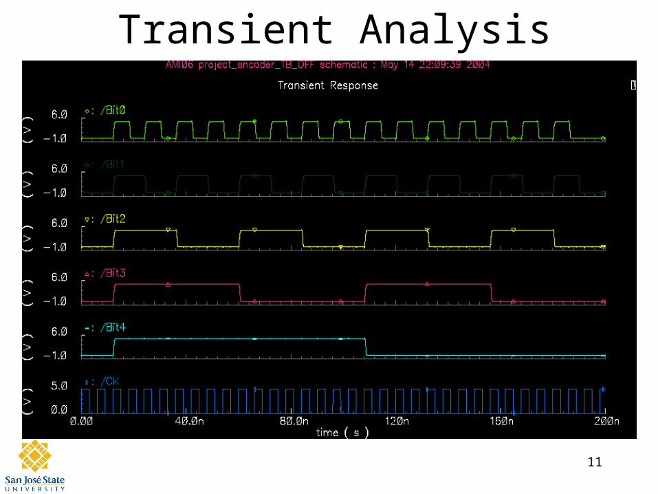
Transient Analysis
12
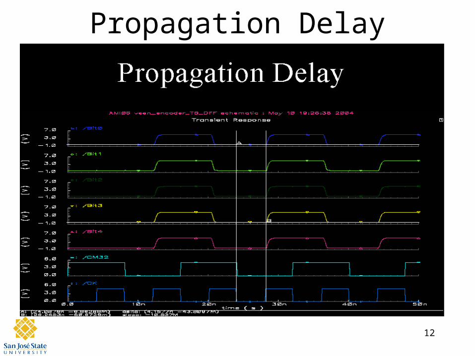
Propagation Delay

13
Layout

14
DRC Check & LVS

15
Cost Analysis
• Time we spent on each phase of the project– verifying logic : 6 Hours– verifying timing : 20 Hours– layout : 30 Hours– post extraction : 1 Hour

16
Summary
• Designed Encoding Logic for 5 bit Analog to Digital Converter without Sample & Hold.
• Designed Conforming to Specifications
• Clock frequency > 200 MHz
• Power < 3mW
• Area : 337.2 um x 104.70 um

17
Reference
• IEEE Paper :
An 8-bit 250 megasample per second analog-to-digital converter: operation without a sample and holdPeetz, B. Hamilton, B.D. Kang, J. This paper appears in: Solid-State Circuits, IEEE Journal of

18
Acknowledgements
• Thanks to Dr. David Parent
• Thanks to Cadence Design Systems for the VLSI lab