0y) o final report - defense technical information center o final report millimeter wave antennas...
TRANSCRIPT

0Y)
o Final Report
Millimeter Wave Antennas
Department of Electrical Engineering
University of Houston
Houston, Texas 77204
September 1, 1984 to August 31, 1988
ARO Project No. 21139-EL
Contract No. DAA.G29-84-K-0166
DTICNV231988f
Dr. Stuart A. LongUDr. David R. Jackson H
88 1122 '8 4
~i~iIBUIONSTATEMADTT A
Approve f or Publc ""C,Dtftribution Unlmrit

DISCLAIMER NOTICE
THIS DOCUMENT IS BEST QUALITYPRACTICABLE. THE COPY FURNISHEDTO DTIC CONTAINED A SIGNIFICANTNUMBER OF PAGES WHICH DO NOTREPRODUCE LEGIBLY.

SECURITY CLASSIFICATION OF THIS PAGE (M7hen Des Entered) MASTER COPY - FOR REPRODUCTION PURPOSES
REPORT DOCUMENTATION PAGE BREADCLTORMI. REPORT NUMBER 2. GOVT ACCESSION NO. 3. RECIPIENT'S CATALOG NUMBER
'a" 139.,-((. N/A N/A4. TITLE (.nd Subtitle) S. TYPE OF REPORT & PERIOD COVERED
Millimeter Wave Antennas Final ReportSept. 1, 1984-Au . 31, 1988
6. PERFORMING ORG. REPORT NUMBER
7. AUTHOR(.) 6. CONTRACT OR GRANT NUMBER(.)
Contract No. DAAG29-84-K0166ARC Project No. 21139-EL
9, PERFORMING ORGANIZATION NAME AND ADDRESS 10. PROGRAM ELEMENT. PROJECT. TASKAREA & WORK UNIT NUMBERS~Department of Electrical EngineeringUniversity of HoustonHouston. Texas 77204-4793
1. CONTROLLING OFFICE NAME AND ADDRESS 12. REPORT DATE
U. S. Army Research Office October 28, 1988
Post Office Box 12211 13. NUISBER OF PAGESRegparch Tr .snl,? P ,r1, NC 977O9 u/
I4. MONITORING AGENCY AME & AD! RESS(If diffe,, fro. Conirolllng Off-c) IS. SECURITY CLASS. (o thl report)
Unclassified
IS. DECLASSIFICATION/DOWNGRADINGSCHEDULE
'6. DISTRIBUTION STATEMENT (of this Report)
Approved for public release; distribution unlimited.
17. DISTRIBUTION STATEMENT (of the abstract entered In Block 20, It different ho. Report)
NA
18. SUPPLEMENTARY NOTES
The view, opinions, and/or findings contained in this report arethose of the author(s) and should not be construed as an officialDepartment of the Army position, policy, or decision, unless soI e.zn tPe hy nthcr dnr,,mntlainn_
IS1. KEY WO RDS (Conflno. or, tev . ~Ida If necessary and Idenilfy by block noonber)
Antennas, millimeter wave, microstrip, dielectric resonator
/,--
20, AMTR ACT M-diu - rae. b If seat n idet Itytl by block -nb-)
1?The properties of two types of antennas suitable for operation at millimeterwave frequencies (100 to 300 GHz) have been investigated both theoretically andexperimentally. The type of radiators considered were printed-circuit or micro-strip antennas and dielectric resonator antennas. Special emphasis was placed onthe problem of integrating the antenna with the waveguiding structure. The ulti-mate objective of the research was to provide aid in the selection and design ofmillimeter wave antennas for given systems applications within this frequencyran. -1 ,,
D j 1473 EiToN O Nov5 (;IS ONSOLFE/ UNCLASSIFIED
- ' . " -1 SECURITY CLASSIFICATION OF THIS PAGE (Wkhen Dae Entered

TABLE OF CONTENTS
Statement of Problem Studied I
Summary of Most Important Results I
List of Publications 5
Papers Published 5
Papers Submitted 7
Papers Presented 9
Participating Personnel I
Degrees Earned II
Appendices 14
A. Dual-Ban Microstrip Antennas with Monolithic ReactiveLoading
B. An Experimental Investigation of Electrically ThickRectangular Microstrip Antennas
C. Reactively Loaded Microstrip Antennas
D. The Input Impedance of the Dielectric ResonatorAntenna
E. An Asymptotic Extraction Technique for EvaluatingSommerfeld-Type Integrals
F. Analysis of Planar Strip Geometries in a Substrate-Superstrate
G. Resonant Frequency of Electrically Thick RectangularMicrostrip Antennas
H. An Improved Formula for the Resonant Frequencies of theTrianglular Microstrip Patch Antenna
I. A Leaky-Wave Analysis of the High Gain Printed Antenna Acoesslon ForConfiguration
NTIS TA& L-
J. Microstrip Transmission Line Excitation of Dielectric TABResonator Antennas Utiawuto,inc ed [1
Di strlbIton/
Avallabil/ty Cor,.-
Diet /SpeciS 3

STATEMENT OF PROBLEM STUDIED
Antennas are being used presently, or have been proposed for use on systems now underdevelopment, on military hardware such as missiles, projectiles, aircraft, satellites, and tanks.They may be used for the purpose of remote guidance, communications, terrain sensing, fusing,navigation, or position location. In recent years the frequency range of interest for military systemshas gradually progressed upward. For several applications today frequencies beyond those of theusual microwave band are required. Of special importance is the millimeter wave regions from100 to 300 GHz (with a resulting wavelength in air of 3.0 to 1.0 mm).
Many of the same properties that are important for more usual microwave antennas arealso required for uses at millimeter wave frequencies. Some of the physicai properties that can beimportant include, ruggedness. ease of fabrication, and the ability to be mounted conformally to theobject on which it is attached. Electrical properties which may be important include efficiency.bandwidth, input impedance. and radiation pattern. In addition to these usual considerations, anew set of criteria also arises. Since the millimeter wave energy is not always guided by standardcoaxial lines, or even rectangular waveguides, additional problems arise in the integration ofsuitable antennas with the desired waveguiding system. Thus the transition region between thewaveguide and the antenna and the particular feeding structure is an important part of the antennadesign problem.
The properties of two types of antennas suitable for operation at millimeter wavefrequencies (100 to 300 GHz) have been investigated both theoretically and experimentally. Thetype of radiators considered were printed-circuit or microstrip antennas and dielectric resonatorantennas. Special emphasis was placed on the problem of integrating the antenna with thewaveguiding structure. The ultimate objective of the research was to provide aid in the selectionand design of millimeter wave antennas for given systems applications within this frequency range.
SUMMARY OF MOST IMPORTANT RESEARCH
I) Dielectric cylinders of very high permittivity have been used in the past as resonantcavities, but since the structure is not enclosed by metallic walls, electromagnetic fields do existbeyond the geometrical boundaries of the structure and part of the power is radiated. Through theproper choice of geometry and permittivity this radiation can become the dominant feature of thestructure and become an efficient antenna for use at millimeter wave frequencies. Bothexperimental and theoretical investigations of a variety of these dielectric resonator antennas havebeen undertaken. In particular. the input impedance of a probe-fed cylindrical structure wasexamined in detail and a comparison of theoretical and exp-rimental results was made. [4]
2) An approximate theory was derived for the modes in a cylindrical dielectric resonatorantenna. The air-dielectric interface was approximated as a perfect magnetic conductor andexpressions for the resonant frequency and radiation from the equivalent surface magnetic currentswere derived. A broad beam with a maximum normal to the ground plane was obtained for thelowest mode. A more directive beam or a beam with a single sharp null was obtained for the nextmode depending on the cylinder geometry. Good agreement was obtained between theory andexperiment.
An experimental investigation was also undertaken to demonstrate that the coplanarwaveguide was an effective excitation mechanism for the cylindrical dielectric resonator antenna.Data showing the coupling behavior and the radiation patterns for various cylinder aspect ratios.dielectric constants. and feed positions were presented. The results show that efficient and practicalantenna systems can be designed using such a feed structure which is much more practical atmillimeter wave frequencies.
3) A systematic investigation of the excitation of a cylindrical dielectric resonator antenna
mira i m ii • I1

by a microstrip transmission line was undertaken to illustrate the possibility of such a feed structureand to characterize the coupling behavior and radiation patterns of the system,[ 8)
4) The electromagnetic properties of electrically thick rectangular nticrostrip antennas wereinvestigated experimentally. Antennas were fabricated with different patch sizes- and with electricalthicknesses ranging from 0.03 to 0.23 wavelengths in the dielectric substrate. The resonantfrequencies were measured and compared to existing formulas. The bandwidth was calculated as afunction of electrical thickness and the antenna radiation patterns were measured.
5) An algebraic formulation for the resonant frequency of a rectangular microstrip antennahas been derived which is valid for electrically thick substrates. Predicted values of resonance arecompared with previous theories, as well as actual experimental measurements. for radiatorsapproaching one-quarter wavelength in thickness. which may correspond to physically thin printedcircuit boards at millimeter wave frequencies.
6) The design and experimental measurement of a dual-band, monolithic toicrostripantenna is presented. The structure utilizes a short-circuited length of microstrip transmission lineto provide reactive loading and. thereby. retains the low-profile characteristic of a normalmicrostrip patch radiator and allows accurate fabrication for high frequency applications.
7) An experimental study of reactively loaded rectangular microstrip antennas has beenundertaken. The reactive loads used were either a single pin. or a symmetrically located pair ofpins, short circuiting points on the patch to corresponding points on the ground plane. A set ofpoints forming a single curve for the case of one shorting pin or two symmetrically located curvesfor the case of two shorting pins was found. A single. or a pair. of short circuits placed at anypoint on these curves results in an element having a fixed resonant frequency and a fixed radiationpattern independent of the point selected. The input impedance. however, varies over a very largerange when the short circuit or pair of short circuits is moved along these curves. The majorapplication of this work is the study of the feasibility of maintaining an impedance match for theelements of a microstrip antenna array with changing scan angle by moving the position of one ormore short-circuiting pins. An experimental and theoretical study of the mutual impedance formicrostrip array elements was conducted and used in a computer program simulating a finite array.Though the model used for mutual impedance was somewhat crude. the simulation programpredicted a variation of active element impedance with scan angle. For a number of different scanangles. the position of shorting pins was adjusted to obtain a match for all of the array elementsthus indicating that this dynamic tuatching technique may be feasible for scanned arrays.
8) A dual mode microstrip antenna element was investigated which had two independentlyexcitable modes resonant at the same frequency. This element has been shown to be capable ofproducing a broadside maximum, a broadside null. or an end-fire type pattern by suitable choicesof its reactive loads and suitable excitation of its degenerate modes. Appropriately located loads canbe used to resonate modes normally resonant at quite different frequencies. at a single. commonfrequency. The results indicate that the nodal lines of the loaded element are accurately predictedby the generalized theory of loaded microstrip antennas, and that two modes can be excitedindependently of each other by feeding each mode along the nodal line of the other. To verify thetheoretical predictions an actual dual mode microstrip element was fabricated and tested. Theresults of this experiment correlate well with the theoretical model for the overall characteristics ofthe radiator.
9) One of the initial studies during this contract concerned the properties of microstripradiators in a two-layered substrate-superstrate geometry. It was observed previously that certainphenomena occur when a printed antenna element is embedded wifhin such a structure. Forexample, a superstrate layer may be dsed to eliminate surface waves excited by a horizontalcurrent element, resulting in 100% efficiency for such an element. A phenomenon termed
2

"radiation into the horizon" may also le produced, in which the far-field radiation pattern ofan element in a layered microstrip geometry may extend down to the horizon with a nonzerovalue. Using this effect, a substrate-superstrate geometry may be chosen so that the radiationpattern from an embedded element will be nearly omnidirectional. Alternatively. a substrate-superstrate geometry may be used to produce the opposite effect, to produce patterns which havenarrow beams. Some of these effects may have practical uses in modifying the properties ofmicrostrip elements, as well as the radiation patterns. For example. in [6] it is noted that usinga superstrate to eliminate the excitation of surface waves may significantly reduce the mutualcoupling between microstrip elements. The effect of a superstrate layer on other types ofmicrostrip elements such as the electromagnetically coupled (EMC) dipole and the microstripline are also discussed in [6].
During tile course of this investigation, a technique for efficiently evaluating theSommerfeld integrals which occur in microstrip analysis was used. which is explained in [5].This technique overcomes most of the difficulty in computing the Sommerfeld integrals forsource and observation points which are widely separated. which would otherwise be a seriouslimitation in the computation of mutual impedance in many cases.
10) One of the main projects which was initiated during this contract was a leaky-waveinvestigation of the narrow-beam effect which may be created in a multiple-layer dielectricgeometry. This project. started with an investigation of the two-layered substrate-superstratestructure, which had already been found previously to produce narrow beams as thepermittivity of the superstrate increases, for a particular choice of layer thicknesses. This effectwas found to be attributable to the existence of weakly attenuated leaky waves which are excitedon the structure in this high-gain condition. The layer thicknesses essentially determine thepropagation constant of the waves, and hence the beam scan angle. while the permittivitydetermines the attenuation of the waves, which in turn determines the beamwidths. Anasymptotic solution of the characteristic equations for the TE and TM leaky waves allowed forclosed-form expressions for the propagation constants. By using scalar radiation theory, radiationpatterns for the case of a two-dimensional source within the structure were obtained. A comparisonwith exact patterns showed excellent agreement near the beam maximum, where the leaky wavescontribute significantly to the total pattern. Details of the analysis, as well as the results, aregiven in [9].
The next phase in the leaky-wave research project was the investigation of themultiple-layer dielectric structure, which consists of an arbitrary even number of layers havingalternating low and high permittivities. It was observed in previous work by others (H. Y. Yangand N. G. Alexopoulos. "Gain Enhancement Methods for Printed Circuit Antennas ThroughMultiple Superstrates". IEEE Tons. Ateninas ['ropagar.. vol. AP-35. pp. 860-863. July 1987) thatvery narrow beams could be obtained when using more than two layers in the structure. Sucha structure may find applications at millimeter-wave frequencies, where the thickness would notbe a serious limitation. A leaky-wave antenna constructed from only dielectric layers, witha simple source mechanism, would have the advantages of durability and simplicity. Aleaky-wave analysis of this structure revealed the same leaky wave behavior as for the two-layered case. A more general analysis technique was developed to calculate the propagationconstants of the leaky waves, however. This technique utilized the similarity in field structurebetween the leaky wave fields and the fields existing inside the layered structure when illuminatedwith a plane wave excitation. A power calculation inside the structure was then used to deriveasymptotic formulas for the leaky-wave propagation conslants. A comparison with exact valuesof propagation constants showed very good agreement. which improves as the beamwidthdecreases. The derivation of these formulas is given in [15].
During the leaky-wave investigation, another topic whichs was explored was theextension of ieaky-wave radiation formulas to the case of cylindrically propagating leakywaves. Previously. leaky-wave radiation formulas existed only for the case of a one-dimensional wave, where the radiation pattern could be determind from a Kirchoff-Huygensscalar radiation equation (T. Tamir and A. A. Oliner. "Guided Complex Waves: Part 2. Relation
3
to Radiation Patterns". l'roc. lEE. vol. I10. pp. 325-334. Feb. 1963). For leaky-wave antennasconsisting of a cylindrical leaky wave propagating on a planar interface. scalar radiationtheory no longer suffices, due to the vector nature of the aperture fields. A microstrip sourcewithin a layered structure is one example where the leaky wave is cylindrical, so it is clearlyimportant from a practical standpoint to have radiation formulas available for cylindricalwaves. By using the equivalence principle and integrating over the equivalent sources, closed-form expressions for the far-field radiation patterns of TE and TM cylindrical leaky waveswere obtained. One practically important aspect of these formulas was that the results allowed forarbitrary aperture size, so that the radiation from a truncated aperture could be studied. This ispractically important. since all planar structures nust be trln cated at some finite radius. Theformulas which were developed were used together with the asymptotic analysis of the multiple-layered structure in order to accurately predict the radiation patterns from sources withinthis structure. The radiation formulas are derived in [14].
I1) Another project which was investigated under the contract was the accuratecomputation of mutual coupling in large phased arrays of patch antenna elements. Thisinvestigation led to a formulation of mutual impedance from which series expansions forthe impedance matrix could be easily obtained. For large sparce arrays, the first few terms ofthis matrix series usually gives accurate results for the patch impedances. while requiringmuch less computation time than the matrix inversion required in a onent-methodformulation of the phased array impedance matrix. A derivation of these series expansions maybe found in [II].
12) Also initiated during the contract was a design study of an array of EMC dipoles. TheEMC dipole is a very promising tiicrostrip element due to its small size and simplicit. Athigher frequencies where the substrate thickness stay be .05 wavelengths or more. the EMCdipole also exhibits a large bandwidth. It also has the advantage of easy matching with tlefeeding transmission line. by simply adjusting the dipole length and offset. An array of theseelements would make an attractive design for many applications. Previously, a design procedurefor an array of such elements was developed by Elliott and Stern (R. S. Elliott and G. J. Stern."The Design of Microstrip Dipole Arrays Including mutual Coupling. Part I: Theory". IEEETrans. Anteitas Propogat., vol. AP-29. pp. 757-760. Sept. 1981). This design procedtre wasmore directly compatible with experimental meastrements than with nsumerical calculation.however. During the present investigation a design procedutre was developed which was well-suited to a direct miotnent-method analysis. One of the key features of this design procedure is
the introduction of coupling coefficients which may be determined nunerically by
considering only two EMC dipole pairs at a titme. resulting in a relatively small momentmethod problem. The use of traveling-wave basis functions on the transmission lines furtherimproved the efficiency of the calculation. Once the coupling coefficients are determined, amatrix description of the line and dipole currents is used to formulate a matrix set of designequations, which accounts for all of the necessary interactions between all of the lines and dipolesin the array. This matrix set of equations allows for the design of a feed network which will excitethe required dipole currents in order to produce a specified radiation pattern. In order to test
the theory. an experinental four element linear array was constructed and tested, with goodagreement between the theoretical and measured patterns, Details of the design procedure.along with the results. may be found in [13],
13) An ;nvestigation of the scattering properties of conductive bodies embedded withinlossy media was undertaken during the contract period. One particular example of such a
configuration would be a microstrip patch antenna on top of or below a lossy dielectric layer. Ageneral scattering formula was derived which shows the fmundamental dependence of the radarcross section of (hie body on the parameters of the lossy meno.a. One important result of thisformula is that the body radar cross section (RCS) is directly related to the radiation efficiency ofthe body. so that the RCS may be directly controlled by introducing loss into a surrounding layer.
4

A numerical study was performed for a rectangular patch antenna embedded within a lossysubstrate-superstrate geometry, as a specific case. Results were obtained for three particularconfigurations: a lossy substrate, a lossless substrate with a lossless superstrate on top, and alossless substrate with a lossy superstrate on top. In each case, the results confirmed the generaltrend predicted by the scattering formula. Details and results may be found in [12).
14) During the contract period a feasibility study of an array of
electromagnetically coupled patch antennas was performed. In this array, the patch antennasare electromagnetically coupled between adjacent neighbors by short sections of transmissionline which are embedded within the substrate. This eliminates the need for a corporate feednetwork, and greatly simplifies the array construction. The feasibility study determined that it ispossible to design such an array to produce a beam scanned to any specified direction, withreasonable coupling values between adjacent patches required. A moment method calculationwas used to determine the coupling coefficients between adjacent patches. and a matrix equationusing these values was then formulated to predict the patch current amplitudes assuming agiven feed source on the first patch and a specified load termination on the last patch. Asynthesis procedure was then developed, whereby the coupling coefficients between adjacentpatches may be determined from the desired set of patch current amplitudes, which determinesthe radiation pattern. Hence. the dimensions of the embedded line sections between the patches aredetermined from the specified pattern. To test the theory. a four element linear array of patches wasbuilt, designed for a 45 beam. The measured pattern showed good agreement with thepredicted result, and demonstrated the feasibility of this type of array. The details of the designtechnique. along with the results. are given in (I I).
15) An investigation of the properties of a traveling-wave array of monopolesembedded within a substrate, fed by a meanderintg stripline. was conducted during the contractperiod. Such an array may make a useful scanned-beam antenna for some applications.Because individual monopoles which are electrically sthort do not radiate significantly. it ispossible to cerstruct arrays of this type many wavelengths long. with control of the monopolecurrents achieved by variation of the monopole heights and length of the meandering striplinebetween monopoles. A quasi-periodic structure analysis of the array was used to obtain designequations for the monopole heights and line lengths required to produce a specified constantphase shift between elements, and a specified amplitude taper in the monopole currents alongthe length of the array, As an experimental verification of the theory, a ten-element linear arraywith a 600 beam was designed and constructd. The measured pattern showed goodagreement with the theoretical one. A detailed discussion of the theory and results may he
found in [2].
LIST OF PUBLICATIONS
PAPERS PUBLISHED
[I] S. E. Davidson. S. A. Long and W. F. Richards. "Dual-Bind Microstrip Antennas withMonolithic Reactive Loading". Electronics Letters. vol. 21. no. 20, pp. 936-937. September 26.1985.
The design and experimental measurement of a dual-band. monolithic microstrip antenna ispresented. The structure utilizes a short-circuited length of micros~rip transmission line to providereactive loading and, thereby, retains the low-profile characteristic of a normal microstrip patchradiator.

[21 F.. Chang. S. A. Long, and W. F. Richards. "Al Experinlenlil Investigation ofElectrically Thick Rectangular Microstrip Antennas" IEEE 7Trans. Anlemias and Propagation. vol.AP-34, June 1986.
The electromagnetic properties of electrically thick rectangular microstrip antennas wereinvestigated experimentally. Antennas were fabricated with different patch sizes and with electricalthicknesses ranging from 0.03 to 0.23 wavelengths in the dielectric substrate. The resonantfrequencies were measured and compared to existing formulas. The bandwidth was calculated as afunction of electrical thickness and the antenna radiation patterns were measured.
[3] W. F. Richards and S. A. Long. "Reactively Loaded Microstrip Antennas," IEEEAnferras and Propagation Society Ne'sletter, vol. 28. No. 5, pp. I I- 17. October 1986.
Microstrip elements have proven to be very versatile and have found uses in a variety ofapplications from satellite arrays to automobile anti-collision warning systems. This versatilitystems mainly from their structural simplicity, ease of construction, ruggedness, conformability, lowprofile. and low cost. In addition to these features. microstrip elements are capable of producing avariety of different patterns and polarization. Most research efforts, however, have been limited tobasic applications using only a single, unperturbed mode of a rectangular or circular element.Additional applications are possible through the used of reactive loading. These include multiband.frequency-agile and polarization-diverse, adaptable-impedance, and multimode-pattern antennas.Some experimental work has been done in these areas but very little theoretical work has beendone. In this paper. a very simple theo.'y is presented which will guide a designer who wished totake advantage of the added flexibility thi;t reactive loading provides. In addition, several applicationare discussed with corresponding theoretical and experimental results.
[41 S. A. Long and M. W. McAllister. "The Input Impedance of the Dielectric ResonatorAntenna". International Journal of Infrared and Millimeter Waves. vol. 7. no.4. pp. 555-570.1986
Dielectric cylinders of very high permittivity have been used in the past as resonantcavities, but since the structure is not enclosed by metallic walls, electromagnetic fields do existbeyond the geometrical boundaries of the structure and part of the power is radiated. Through theproper choice of geometry and permittivity this radiation can become the dominant feature of thestructure and become an efficient antenna for use at millimeter wave frequencies. Bothexperimental and theoretical investigations of a variety of these dielectric resonator antennas havebeen undertaken, In particular. the input impedance of a probe-fed cylindrical structure wasexamined in detail and a comparison of theoretical and experimental results was made.
[5] D. R. Jackson and N. G. Alexopoulos. "Arn Asymptotic Extraction Techniquefor Evaluating Sommerfeld-Type Integrals". IEEE Transactions oi Antennas a1d Propagaion.vol. AP-34. pp. 1467-1470. Dec. 1986.
An asymptotic extraction technique is developed. which leads to an efficient evaluation ofthe electric field from a Hertzian dipole in a layr -ed geometry. This technique allows for arapidly converging expression for the electric field. which remains well behaved as the sourceand observation heights above the ground plane coincide. A useful application of this method isin the calculation of mutual impedance between printed dipoles.
[61 D. R. Jackson and N. G. Alexopoulos. "Analysis of Planar Strip Geometries ina Substrate-Superstrate Configuration". IEEE 7ransactions ol Artennas and Propagation. vol. AP-34. pp. 1430-1438. Dec. 1986.
6
A moment method procedture is nsed to analy1ze the nehavior of several differentconfigurations consisting of planar strips in a substrate-superstrate geometry These includethe microstrip transmission line.center-fed dipole, the mutual impedance between two dipoles. and the transmission-linecoupled dipole. In each case some of the basic superstrate effects are discussed.
[7] R. Garg and S. A. Long, "Resonant Frequency of Electrically Thick RectangularMicrostrip Antennas" Electronics Letters, vol. 23. no. 21, pp. 1149-1151. Octobel 8. 1987.
An algebraic formulation for the resonant frequency of a rectangular microstrip antennashas been derived which is valid for electrically thick substrates. Predicted values of resonance arecompared with previous theories, as well as actual experimental measurements, for radiatorsapproaching one-quarter wavelength in thickness.
[8] R. Garg and S. A. Long. "An Improved Formula for the Resonant Frequencies of theTriangular Microstrip Patch Antenna". IEEE Trans. on Antennas and Propagation. vol.AP- 36.no. 4. pp. 570-575, April 1988.
An improved formula is derived to predict the resonant frequency of the triangularmicrostrip patch antenna. The techni- ue previously used for the case of a circular disk is modifiedto produce greater accuracy than pre ious investigations.
[9] D. R. Jackson and A. A. Oliner. "A Leaky-Wave Analysis of the High-Gain PrintedAntenna Configuration". IEEE Transactions on Antennas and Propagation, vol. AP-36. July1988.
A leaky-wave analysis is used to explain the narrow-beam "resonance gain" phenomenon.in which narrow beams may be produced from a printed antenna element in a substrate-superstrate geometry. The leaky-wave approach furnishes insight into the physical nature of thisphenomenon, as well as providing new practical information. The leaky-wave approach alsopermits the derivation of simple asymptotic formulas for the leaky-wave propagation constants.which determine the radiation patterns.
[10] R. A. Kranenburg and S. A. Long "Microstrip Transmission Line Excitation ofDielectric Resonator Antennas". Electronics Letters. vol. 24. no. 18. pp. 1156-1157, September I.1988.
A systematic investigation of the excitation of a cylindrical dielectric resonator antenna wasundertaken to illustrate the possibility of such a feed structure and to characterize the couplingbehavior and radiation patterns of the system.
PAPERS SUBMITTED
(11] D. R. Jackson. W. F. Richards. and A. Ali-Khan. "Series Expansions for the Mutual
Coupling in Microstrip Patch Arrays". tEEE Tratsactions on Antentas and Propagation (acceptedfor publication).
A dominiat-node iurntual coupling theory is developed for an1 array of microstrip patches. Aformulation is used which is compatible with either a cavity model or a spectral-domain
7

calculation, or with measurements. Th's formulation allows for the simple derivation of series
expansions for the impedance. admittance, and scattering matrices, which do not requireinversion of a moment-method matrix. These expansions are computationally efficient for large.sparce arrays.
[12] D. R. Jackson. "The RCS of a Rectangular Microstrip Patch in a Substrate-Superstrate Geometry". IEEE Transactions on Antennas ald Propagation (accepted forpublication).
A general scattering formula is developed for the radar cross section of a general resonantconductive body embedded within lossy media. This formula shows that the RCS of the body isdirectly related to the radiation efficiency of the body. The specific case of a rectangular microstrippatch within a Iossy substrate-superstrate geometry is analyzed, with results presented for threedifferent cases: a lossy substrate only. a lossless substrate with a lossless superstrate. and alossless substrate with a lossy superstrate. It is concluded that the lossy superstrate case givesthe most RCS reduction with the least detrimental effect on the input impedance of the patch.
[131 D. R. Jackson, A. E. Diiibergs. and S. A. Lonig. "A Moment Method Design Procedurefor an Array of EMC Dipoles". submitted to IEEE Transactions on Antennas and Propagation.
A design procedure based on a moment-method analysis is given for an array of microstripdipoles electromagnetically coupled (EMC) to microstrip transmission lines. One -)f the key featuresof the design procedure is that only one pair of EMC dipoles needs to be analyzed at a timenumerically, in order to develop the necessary coupling coefficients which account ,or theinteractions between all of the EMC line-dipole pairs. A convenient set of matrix design equationsare obtained, which allows for the design of a feed network to excite the desired dipole currents.
[14] A. Ip and D. R. Jackson. "Radiation from Cylindrical Leaky Waves". submitted toIEEE Traiisactions onl Anteinas and I'ropagatioi.
Formulas for the far-field paitern of cylindrical leaky waves propagating on a plaiiarsurface are derived. These formulas may be used to predict the radiation pattern of a generalclass of leaky-wave antennas, consisting of a finite-size source which excites a radiallypropagating leaky wave on some planar surface. Leaky-wave antennas comprised ofmicrostrip antenna elements fall into this category. Formulas are derived for both TE and TMleaky waves of arbitrary aperture size, which allows the practical effects of a truncated aperture tobe determined.
[15] D. R. Jackson. A. A. Oiner. and A. Ip. "Leaky-Wave Propagation and Radiation fora Multiple-Layer Dielectric Structure". submitted to IEEE Transactionls an Antennas andPropagation.
A leaky-wave analysis is used to predict the beamwidth of a narrow-beam multiple layerdielectric structure. consisting of an alternating arrangement of low and high permitti,,itvdielectric layers. A power-flow analysis is used to derive asymptotic formulas for the phaseand attenuation constants of the leaky waves which propagate on this structure. which directlydetermines the beamwidths and scan angle. The asymptotic formulas show that the bean widthdecreases very rapidly as the number of layers increases, so that very narrow beams may beobtained with only a modest number of laye;s.
[16] H. Y. Yang. N. G. Alexopoulos. and D. R. Jackson. "Microstrip Open-End and Gap
8
L

Discontinuities in a Substrate-Superstrate Structure", submitted to IEEE Transaclions onMicrowave theory and 7T'chniques.
An analysis of both open-end and gap discontinuities in microstrip lines within a substrate-superstrate geometry is given. The analysis uses both subdomain and semi-infinite traveling-wavebasis functions for an efficient mnoment-nethod calculation of the scattering parameters.Results show that the superstrae may significantly affect the discontinuity parameters, byincreasing the space wave and surface-wave radiation at the discontinuity.
[17] 11. 3. Katehi. 1). IK. ,tackson. and N. G. Alexopotlos. "Microsirip Dipoles",submitted as Chapter 5 of The Handbook of Microstrip Antennas. J. R. James and P. S. Hall.Eds.
A general overview of the analytic and numerical aspects of modeling microstrip dipoleconfigurations is presented, along with results showing sone of the basic properties of themicrostrip dipole. Particular attention is devoted to the EMC dipole, both as a single element and asan element in a finite array. Practical considerations include bandwidth and impedance behavior.and the trade-off between dipole bandwidth and line radiation for the EMC dipole.
(18] R. A. Kranenburg. S. A. Long and .. T. Williams, " Coplanar Waveguide Excitationof Dielectric Resonator Antennas". IEEE Transactions on Aennas and I'ropagatio.
An approximate theory is derived for the nodes in a cylindrical dielectric resonatorantenna. The air-dielectric interface is approximated as a perfect magnetic conductor andexpressions for the resonant frequency and radiation from the equivalent surface magnetic currentsare presented. A broad beam with a maximum nornial to the ground plane is obtained for thelowest mode. A more directive bean or a beam with a single sharp null is obtained for the nextmode depending on the cylinder geometry. Good agreement is obtained between theory andexperiment. An experimental investigation was also undertaken to demonstrate the coplanarwaveguide as an effective excitation mechanistm for the cylindrical dielectric resonator antenna.Data showing the coupling behavior and the radiation patterns for various cylinder aspect ratios.dielectric constants. and feed positions are presented. The results show that efficient and practicalantenna systems can be designed.
PAPERS PRESENTED
[I] S. A. Long, 'Dielectric Resonator Antennas" presented at U. S. Army Research OfficeWorkshop on Millimeter Wave Technology. New York Institute of Technology. Old Westbury.NY. December 1984.
[2] S. E. Davidson S. A. Long. W. F. Richards. "Monolithic Design of Dual-Band MicrostripAntennas Using Reactive Loading" presented at IEEE International AP-S Symposiun, Vancouver,British Colutmbia, June 1985.
[31 W. F. Richards and S. A. Long, "Pattern Adaptation Using Loaded Dual-Mode MicrostripAntennas presented at IEEE Internatiortal AP-S Symposium. Vancouver. British Columbia. June1985.
141 M. W. McAllister and S. A. Long. "'e l)ielectric Resonalor Antenna". piesented at IcnthInternational Conference on Infrared and Millimeter Waves. Lake 9uena Vista. Florida. December1985.
9

[51 W. F. Richards and S. A. Long, "r!;pedance Matching of Microstrip Antcnnaw with ReactiveLoads" presented at National Radio Scienc- Meeting, Boulder. Colorado. January 1986.
[61 E. Chang, S. A. Long and W. F. Richards. "The Resonant Frequency of Electrically ThickRectangular Microstrip Antennas" presented at IEEE International AP-S Symposium. Philadelphia.PA, June 1986.
[7] W. F. Richards and S. A. Long. "Matching Microstrip Antennas Using Reactive Loads"presented at IEEE International AP-S Symposium. Philadelphia. PA. June 1986.
[8] D. R. Jackson and S. A. Long. "A Moment-Method Approach for the Array or t'ransmissionLine Coupled Dipoles", presented at the IEEE AP-S Intl. Syrmp.. Philadelphia, PA. June 1986,
[9] D. R. Jackson and N. G. Alexopoulos. "An Asymptotic Extraction Technique for the Real-Space Evaluation of Sonrnerfeld-Type Integrals". presented at the URSI National Radio ScienceMeeting. Philadelphia. PA. June 1986.
[10] S. A. Long. "The Cylindrical Dielectric Resonator Antenna" prcrnted at the U. S. ArmyResearch Office Workshop on Fundamental Issues in Millimeter and Submillimeter Waves. LosAngeles. CA, September 1986.
[Ill W. F. Richards and S. A. Long. "Impedance Control of Microstrip Antennas UtilizingReactive Loading" presented at International Telemetering Conference. Las Vegas. NV. October1986.
[12] W. F. Richards and S. A. Long, "Adaptive Pattern Control of a Reactively Loaded Dual-ModeMicrostrip Antenna" presented at International Telemetering Conference, Las Vegas, NV, October1986.
[13] D. R. Jackson. W. F. Richards, and A. Ali-Khan. "An Exact Mutual Coupling Theory forMicrostrip Patches", presented at the IEEE AP-S Intl. Symp.. Blacksburg. VA. June 1987.
[14] D. R. Jackson and A. A. Oliner. "A Leaky Wave Analysis of the High-Gain PrintedAntenna Configuration", presented at the URSI Radio Science Meeting. Blacksburg. VA.June 1987.
[15] S. A. Long, "An Investigation of the Use of Reactive Loading to Control the Impedance ofMicrostrip Antennas" presented at Missite/Projectile/Ai rhorne Test Instrumentation AntennasWorkshop. Atlanta, GA. October 1987.
[16] S. A. Long and A. Ali Khan. "An Investigation of the Impedance of Reactively LoadedMicrostrip Antennas" presented at National Radio Science Meeting. Boulder. Colorado. January1988.
[17] N. G. Alexopoulos. H. Y. Yang. and D. R. Jackson. "Analysis of Microstrip Open-End andGap Discontinuities in a Substrate-Superstrate Configuration". presented at the IEEE MTT-S Intl.Symp.. New York City. NY, May 198 .
[18) D. R. Jackson and N. G. Alexopoul-s. "Scattering from a Microstrip Patch in a LossySubstrate-Superstrate Geometry". presented at tire IEEE AP-S Intl, Symp., Syracuse. NY. June1988.
[19] D. R. Jackson. A. A. Oliner, and A. Ip. "Radiation from Leaky Waves on Multiple-LayerDielectric Structures". presented at the URSI Radio Science Meeting. Syracuse. NY. June 1988.
10

PARTICIPATING PERSONNEL
Stuart A. Long, ProfessorWilliam F. Richards, Associate ProfessorDavid R. Jackson. Assistant ProfessorJeffery T. Williams. Assistant ProfessorRamesh Garg. Visiting Associate Professor
Esin Chang. Graduate Research AssistantArturs Dinbergs. Graduate Research AssistantAntonio Ip. Graduate Research Assistantiia-Xiang iang, Graduate Research AssistantAjaz All Khan, Graduate Research AssistantRoger Kranenburg. Graduate Research AssistantSai Kwok. Graduate Research AssistantPrakash Manghnani. Graduate Research AssistantSteve Slawson. Graduate Research AssistantS. Toomsawasdi. Graduate Research Assistant
DEGREES EARNED
(I) E. Chang, "An Experimental Study of Electrically Thick Rectangular MicrostripAntennas," M.S.E.E., University of Houston, December 1985.
The electromagnetic properties of electrically thick rectangular microstrip antennas areinvestigated. Antennas are fabricated with different patch sizes and with electrical thicknessesranging from 0.03 to 0.23 wavelengths in the dielectric substrate. The resonant frequency andbandwidth are measured and compared to existing theories. The radiation patterns are alsomeasured and the 3 dB beamwidths for the antennas are determined.
(2) S. Toomsawasdi. "Moment Method Analysis of a Microstrip Antenna Using a Patch-EdgeIntegral Equation", Ph.D. University of Houston. May 1987.
A method of computing the input impedance of a microstrip antenna in free space and in amodified environment is presented. A pair of integral equations in terms of the patch-edge electricand magnetic currents are solved using the method of moments. One of these integral equations isbased on an approximate exterior-region Green's function. An appropriately chosen magneticcurrent distributed on the side of a conducting mesa in the presence of the dielectric is capable ofreproducing the exact field of a patch element. This mesa is formed by connecting the edge of thepatch to the ground plane with conductor. The approximate Green's function used in this theoryignores the presence of both the dielectric substrate and the conducting mesa. It is. therefore, justthe free-space Green's function and its use instead of an exact Green's function considerablyreduces the computational complexity of the analysis. Results for the input impedance computedusing other approximate theories and measurements are presented for comparison with this theory.Comparison with measured results shows the this theory, though approximate, very accuratelypredicts the locus of the input impedance of microstrip arennas of practical thicknesses.Surprisingly, the antenna quality factor was also predicted very accurately by this techniquealthough the approximate Green's function cannot account for the presence of a surface wave. The
11

resonant frequencies predicted by this theory are somewhat higher than those measured, an effectattributable to ignoring the presence of the dielectric. The approximate Green's function was alsomodified to account for the presence of an elevated dielectric slab for applications to microstripimage arrays. Measurements were made for an element in this modified environment;theoretically predicted impedances agreed well with the measured results.
(3) A. Ali Khan. "Study of Loaded Microstrip Antennas and Their Application To Arrays."M.S.E.E., University of Houston. December 1987.
An experimental study of reactively loaded rectangular microstrip antennas is presented inthis thesis. The reactive loads used here were either a single pin. or a symmetrically located pairof pins, short circuiting points on the patch to corresponding points on the ground plane. A set ofpoints forming a single curve for the case of one shorting pin or two symmetrically located curvesfor the case of two shorting pins was found. A single or a pair. of short circuits placed at anypoint on these curves results in an element having a fixed resonant frquency and a fixed radiationpattern independent of the point selected. The input impedance. however. varies over a very largerange when a short circuit or pair of short circuits is moved along these curves. The majorapplication of this work is the study of the feasibility of maintaining an impedance match for theelements of a microstrip antenna array with changing scan angle by moving the position of one ortwo short-circuiting pins. An experimental and theoretical study of the mutual impedance formicrostrip array elements was conducted and used in a computer program simulating a finite array.Though the model used for mutual impedance was somewhat crude, the simulation programpredicted a variation of active element impedance with scan angle. For a number of different scanangles. the position of shorting pins was adjusted to obtain a match for all of the array elementsthus indicating that this dynamic matching technique may be feasible for scanned arrays.
(4) Antonio Ip. "Radiation and Propagation of Cylindrical Leaky Waves on a PlanarDielectric Multi-Layer Structure", M.S.E.E.. University of Houston. May 1988.
Radiation formulas for cylindrical leaky waves on a planar surface are derived. These formulaspredict the far-field patterns of either TE or TM waves, with an arbitrary finite-sized apertureassumed, so that the effects of aperture truncation may be determined. A narrow-beam antennaobtained by embedding a printed antenna element within a Inuliplc-layer dielectric structnre isthen explained from the existence of weakly attenuated leaky waves which exist on this structure.Analytical methods for asymptotically calculating the leaky-wave propagation constants for smallbeamwidths are presented. Radiation patterns based on the leaky waves are compared with theexact patterns for horizontal and vertical electric and magnetic dipoles in the structure, withexcellent agreement obtained near the beam maximum, where the leaky wave contribution is mostsignificant.
(5) Sai C. Kwok. "Analysis and Design of a Traveling-Wave Array of VerticalMonopoles in a Substrate", M.S.E.E.. University of Houston. Aug. 1988.
This thesis presents an analysis and design technique for a traveling-wave array of monopolesembedded within a substrate, fed by a meandering stripline. A Block analysis is used to analyzethe structure, which is approximated as a periodically loaded trancmission line. with the loadsbeing the active impedances of the monopoles. An iterative design procedure is established whichdetermines the necessary monopole heights and meandering line section lengths in order toproduce a desired inter-element phase shift and current amplitude taper for the set of monopolecurrents, and hence a desired radiation pattern. Special attention is devoted to the efficientevaluation of the Sommerfeld integrals which are needed in tie self and mutual impedancecalculations. As an experimental verification of the theory, a ten element linear array is built
12
and tested, with good agreement obtained between theory and experiment.
(6) Arturs E. Dinbergs, "Analysis and Design of an Array of ElectromagneticallyCoupled Microstrip Dipoles", M.S.E.E.. University of Houston, Aug. 1988.
This thesis presents an analysis and design technique for an array of microstrip dipoleselectromagnetically coupled to microstrip lines (EMC dipoles). A general analysis techniqueusing a combination of piecewisesinusoidal and traveling-wave basis functions is used to analyze the coupling between elements inthe array. A design approach is formulated in which coupling coefficients between only twoisolated EMC dipole elements are needed. These coefficients are used together with a matrixdescription of the line and dipole currents in the array in order to account for the necessarymutual interactions between all of the elements in the array. A four element linear array is builtand tested, with good agreement obtained between the predcted and measured patterns.
(7) Prakash Manghnani. "Design and Analysis of an Array ofElectromagnetically Coupled Microstrip Patches". M.S.E.E.. University of Houston, Aug.1988.
In this thesis, an analysis and design of an array of microstrip patches that areelectromagnetically coupled by transmission lines embedded within the substrate is presented. Amethod of moments formulation is used to calculate the coupling coefficients between elements.using piecewise sinusoidal basis functions on the transmission lines and dominant-mode cavitybasis functions on the patches. An analysis procedure is then developed in which thecoupling coefficients between adjacent elements are used in a matrix equation which thendetermines the patch current amplitudes on all of the elements in the array. A synthesisprocedure is then developed, in which the coupling coefficients are determined in order to producea desired set of patch currents, which determines the radiation pattern. A four element linear arrayhaving a 45 beam is built and tested, with the measured far-field pattern showing goodagreement with the predicted pattern.
(8) Roger Kranenburg "Planar Transmission Line Excitation of Dielectric ResonatorAntennas", M.S.E.E.. University of Houston. November 1988.
An approximate theory is derived for all the modes in a cylindrical dielectric resonatorantenna. The air-dielectric interface is approximated as a perfect magnetic conductor andexpressions for the resonant frequency and radiation from the equivalent surface magnetic currentsare presented. A broad beam with a maximum normal to the ground plane is obtained for thelowest mode. A more directive beam or a beam with a single sharp null is obtained for the nextmode depending on the cylinder geometry. Good agreement is obtained between theory andexperiment.
An experimental investigation was also undertaken demonstrating the microstriptransmission line and the coplanar waveguide as effective excitation mechanisms for the cylindricaldielectric resonator antenna. Results showing the coupling behavior and the radiation patterns forvarious cylinder aspect ratios, dielectric constants, and feed positions are presented. The resultsshow these feed structures may result in efficient and practical antenna systems.
13

Introaucton i or a vanety of applications in lelecomrnunica-tions it is often necssary to utilise two separate operatingAPPENDIX A frequencies. Previous work 2 has shown that a single micro-strip radiating element could be used in this fashion byemploying reactive loading. A general theory has been formu-lated and preliminary experimental measurements have beenmade for radiators using a variable-length, shor!-circuitedcoaxial stub as the mechanism for the loading.' These investi-gations have demonstrated the general techniques involvedand have verified the accuracy of the analysis in predicting theresonant frequencies of the structure.
The presence of the coaxial load which protrudes into theregion behind the low-profile, printed-circuit antenna isusually not desirable in practical systems. For this reasonalternative forms of loading which are monolithic in natureand thus retain the low-profile characteristics of the moreusual single frequency microstrip antenna have been investi-gated. A set of antennas have been designed and tested whichuse microstrip transmission lines etched on the same printed-circuit board as the patch radiator for the reactive loading.Such a structure has been shown to display dual-band behav-iour while retaining the usual, quite attractive physical charac-teristics of a microstrip radiator.
Fig. I Geometry of monolithic design
Design: To model most simply the previously investigatedcosxially loaded antennas one can straightforwardly substi-tute a short-circuited mscrostrip line attached to the edge of a
rectangular patch element. Use at a coaxial load was consider-ably more flexible, however. since the separation between res-onances as well as the resonant trequencies themselves couldalso be adjusted by moving the load position away tram theedge. To emulate this variation the microstrip line has alsobeen designed with a specified "inset' dimension S as shown inFig. I. Unfortunately, positioning the toad in the interior ofhe patch results in yet another parameter G, the gap spacing
between the line and ohe radiator. This parameter seems tohave little effect on the upper resonance but tends to reducethe lower resonant frequency as the gap spacing is increased.The effect of the inset distance, however, is precisely the sameas for the coaxial loads. As the inset is increased, the tworesonant frequencies come closer together, thereby reducingthe overall separation between resonances.
Results: Several antennas were fabricated with varying insetsand gap spacings with stub iengths predicted by theoreticalcalculations to give dual-band behaviour. Two illustrative
&Q1M"&6 - tJ, S 4cst A.
50 -
DUAL-BAND MICROSTRIP ANTENNAS Q:"WITH MONOLITHIC REACTIVE LOADING
-50 -The design and ef a dual-band, 20 0 2, s€oo 2O
m o o lich c rn icr n te n n a is p T h e stru c tu re " q m A ..c v 14 H Zaiilis n-circite egth or microsirip son
p roeractiv loading andi, there by, retains t he 1 -0- Fi. 2 Inmped-'ve of ,dge-load.d 4 x 6 inm patch antenna
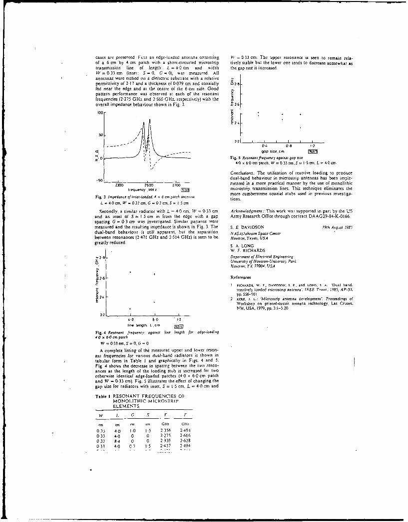
cases are presented. First an edge-loaded antenna consisting 1-V = 0-33 cm. The upper resonance is seen to remain rela-of a 6 cm by 4 cm patch with a short-circuited n-icrostrip tively stable but the lower one tends to decrease somewhat astransmission line of length L = 40 cm and width the gap size is increased.W = 0-33 cm (inset: S = 0, G = 0), was measured. Allantennas were etched on a dielectric substrate with a relativepermittivity of 2.17 and a thickness of 0.079 cm and coaxially o2-5fed near the edge and at the centre of the 6 cm side. Goodpattern performance was observed at each of the resonantfrequencies (2.275 GHz and 2 666 GHz, respectively) with theoverall impedance behaviour shown in Fig. 2. 2-6
t5
50 / i 242
S2"2 ___________I____I____________
04 0-8 -2gap Sizec m
xa" 0 tFig. 5 Resonant frequency against gap sizet 4-0 x 6-0 cm patch, W = 0-33 cm, S = 1-5 can, L = 4-0 am
Conclusions: The utilisation of reactive loading to produce
50 L50 dual-band behaviour in microstrip antennas has been imple-2300 2500 2700 mented in a more practical manner by the use of monolithic
trequency .MHZ F microstrip transmission lines. This technique eliminates themore cumbersome coaxial stubs used in previous investiga-
Fig. 3 Impedance of inset-loaded, 4 x 6 cm patch antenna tions.L 4.0 cm, K' = 0.33 cm, G = 0.3 cm, S = 1-5 cn
Secondly, i similar radiator with L = 4-0 cm. W = 0-33 cm Acknowledgment: This work was supported in part by the USand an inset of S = 1-5 cm in from the edge with a gap Army Research Office through contract DAAG29-84-K-0166.spacing G = 0-3 cm was investigated. Similar patterns weremeasured and the resulting impedance is shown in Fig. 3. The S. E. DAVIDSON 19th August 1985dual-band behaviour is still apparent, but the separation NASA/Johnson Space Centerbetween resonances (2-471 GHz and 2.514 GHz) is seen to be Houston. Texas, USAgreatly reduced. S. A LONG
W. F. RICHARDS
'-2- Department of Electrical EngineeringoUniversity of Houston-Universiry Park
Houston, TX 77004, USAc
,2.6 -References
RICHARDS, . F., DAVIDSON. S. E. and LONG, S A: 'Dual band,reactively loaded microstrip antenna'. IEEE Trans.. 1985, AP-33,pp. 556-5612
4 2 KERR, . L: 'Microstrip antenna development'. Proceedings ofWorkshop on printed-circuit antenna technology, Las Cruces,NM, USA, 1979, pp. 3:1-3:20
4 0 8.0 1 2
Iite tth L .enm F___
Fig. 4 Resonant frequency against line length for edge-loading4-0 x 6-0 em patch
W -0-33 cm, S = 06 = 0
A complete listing of the measured upper and lower reson-ant frequencies for various dual-band radiators is shown intabular form in Table I and graphically in Figs. 4 and S.Fig. 4 shows the decrease in spacing between the two reson-ances as the length of the loading stub is increased for twootherwise identical edge-loaded patches (4-0 x 6-0 cm patchand W = 0-33 cml. Fig. 5 illustrates the effect of changing thegap size for radiators with inset, S = 1-5 cm, L = 4-0 cm and
Table I RESONANT FREQUENCIES OFMONOLITHIC MICROSTRIPELEMENTS
W L G S F r
en en M-n n Gil, Gi ,
0-33 4.0 1-0 I5 2-356 2-4940-33 4.0 0 0 2-275 2-666033 5.4 0 0 2-339 2-6280-33 4-0 0-7 15 2-437 2-494

APPENDIX BIEEE TRANSACTIONS ON ANTENNAS AND PROPAGATION. VOL. AP-34. NO. 6. JUNE 1986 767
An Experimental Investigation of Electrically ThickRectangular Microstrip Antennas
ESIN CHANG, MEMBER, IEEE, STUART A. LONG, SENIOR MEMBER, IEEE, AND WILLIAM F. RICHARDS, MEMBER, IEEE
Abstract-The electromagnetic properties of electrically thick rectan- developed for predicting the resonant frequency of electricallygular microstrip antennas were investigated experimentally. Antennas thin rectangular microstrip antennas.were fabricated with different patch sizes and with electrical thicknessesranging from 0.03 to 0.23 wavelengths in the dielectric substrate. Theresonant frequencies were measured and compared to existing formulas. U1. EXPERIMENTAL PROCEDURESThe bandwidth was calculated as a function of electrical thickness and theantenna radiation patterns were measured. The microstrip antennas investigated are rectangular
patches with geometry as illustrated in Fig. 1. They arefabricated on 3M CuClad 233 and on Rogers RT/duroid 5870
I. INTRODUCTION microwave substrates. The CuClad material is made of a
D URING THE PAST TEN YEARS, microstrip antennas polytetrafluoroethylene (PTFE) woven glass laminate materialexperienced a great gain in popularity and have become a while the RT/duroid material is made of a glass microfiber
major research topic in both theoretical and applied electro- reinforced PTFE composite. Both substrates have a nominalmagnetics. They are well known for their highly desirable dielectric constant (,) of 2.33, and all the antennas are fedphysical characteristics such as low profile, light weight, low using an SMA coaxial feed. In this investigation the feed iscost, ruggedness, and conformability. Numerous researchers located at the midpoint of the longer side (x' = a/2) and at ahave investigated their basic characteristics and recently distance from the edge (y' = 0.15 cm). In each case theextensive efforts have also been devoted to the design of dimension "a" has been chosen to be approximately one and"frequency agile," "polarization agile," or dual-band mi- one-half times the dimension "b" with a 10 cm x 10 cmcrostrip antennas [1], [2], [3]. Most of the previous theoretical ground plane. Two sets of regular microstrip antennas haveand experimental work has been carried out only with been fabricated. The ones in the first set have the sameelectrically thin microstrip antennas. Recent interest has substrate thickness "h" but have nine different patch sizes;developed in radiators etched on electrically thick substrates. the ones in the second set have the same patch size but haveThis interest is primarily due to two major reasons. First, as three different substrate thicknesses. In addition a so-calledthese antennas are used for applications with increasingly "air-dielectric" model radiator has been fabricated to allow anhigher operating frequencies, and consequently shorter wave- even more detailed study of the resonant frequency. Itslengths, even antennas with physically thin substrates become geometry models that of the regular rectangular microstripthick when compared to a wavelength. Second, microstrip antenna shown in Fig. I but with a substrate whose height canantennas have inherently narrow bandwidths and are normally be changed by placing sheets of styrofoam ((, - 1.05) withnot suitable for broad bandwidth applications. Increasing the varying thicknesses between the ground plane and the radiat-bandwidth is possible, but the methods used 14], [5], [6] ing patch. The 1.78 cm x 2.67 cm aluminum radiating patchinvariably increase the volume of the antenna by either has a thickness of t = 0.16cm and is coaxial fed over a 14cmextending the radiating surface or by increasing the overall x 14 cm aluminum ground plane. This fixture allows theantenna thickness. To aid in the design of broader band resonant frequency to be measured for a wide range ofmicrostrip antennas, a careful experimental study of the electrical thicknesses using exactly the same rectangularresonant frequency, bandwidth, and radiation patterns of radiating patch.rectangular microstrip antennas as a function of electrical The resonant frequency, impedance and radiation pattemthickness of the substrate was undertaken. The measured measurements were all performed at the University of Hous-resonant frequencies were compared to formulas previously ton-University Park, Applied Electromagnetics Laboratories,
using an automated network analyzer system and dedicatedManuscript received October 4. 1985; recvi.ed tcc,,bcr 23. 1985. This computer programs. Accuracy enhancement techniques [7)
work was supported in part by the U.S. Army Research Office under Contract have been used to partially correct for effective directivity,DAAG-29-84-K-0166.
E. Chang was with th Department of Electrical Engineering, University of effective source match, and frequency tracking errors whenHouston-University Park. Houston, TX. He is now with the Information taking impedance measurements. The radiation pattern mea-Center, Shell Oil Company, P. 0. Box 20329, Houston, TX 77025. surements were taken with the antenna under test placed inside
S. A. Long and W. F. Richards are with the Department of ElectricalEngineering, University of Houston-University Park, Houston, TX 77004 an anechoic chamber and mounted on a one meter diameter
IEEE Log Number 0608073. circular aluminum ground plane.
0018-926X/86/0600-0767$01.00 © 1986 IEEE

768 IEEE TRANSACTIONS ON ANTENNAS AND PROPAGATION. VOL. AP-34. NO 6. JUNE 1986
ISO
10cm X 10 cm GNO pLaneR
0 0E
radiatingeLement b
E
T x. -- t 0 ... I.......................... .. ....... ...6.3 6.5 5.7 6.9 7.1 7.3
Frequency (GHz)feedpotnt Fig. 2. Comparison of measured and smoothed impedance (I.I m. x 1 7
cm radiating patch, 0.3175 cm substrate, E, = 2.33).
",I. j, B. Resonant Frequency
'dieLectric ' Generally, the resonant frequency ofa microstrip antenna is....ae3"';;-,,?.. ,,,.,,,,,''';' defined as the frequency at which the reactance is equal tozero. For electrically thin antennas, this point is al_ o very
-/... ,l..,,, 1 lose to the frequency where the resistance reaches a maxi-h mum. However, in this investigation many of the reactance
TY Mt connector curves exhibit an inductive shift due to the coaxial feed passingFig. I Rectangular microstrip antenna geometry. through the electrically thick substrate [8], [9]. In fact. for tihe
thicker antennas, the reactance cur'c never passes throughzero at all (see Fig. 2). For this reason, the resonant frequency
Ill. EXPEFMENTAL RESULTS has been redefined as the point at which the resistance reaches
A. Impedance a maximum, independent of the value of reactance. Further-During the course of this research, the input impedances (Z more, since the bandwidth of an electrically thin microstripDRi+;)ang the rsedoftin ptteresrch, the input dances antenna is commonly defined in terms of the impedance (and
= R + jX) and the radiation patterns of each of the antennas thus is dependent on the reactance), an alternate definition of
have been measured. Before the impedance data were used to bd th is not acte by ten te shift ofdetemin th reonan frquecie (f) an th badwithsbandwidth that is not affected by the inductive shift of thedetermine the resonant frequencies (f,) and the bandwidths
reactance is used to obtain the antenna bandwidths of this(BW), they were smoothed in order to take out any residual paper. This last point will be dscussed in detail in a laterripples or oscillations that are due to reflections internal to the section.measurement equipment and have not been corrected by the Set.accuracy enhancement routines. The values of admittance, Y frequency is the effect of the changing electrical thickness of= G + jB, as a function of frequency (f) were computed the substrate, a normalized resonant frequency is definedfrom the measured impedance versus frequency data through where fo,0 = .,/fs, and fo is the zeroth-order prediction ofthe relation Y = Z- '. Depending on the values of admittance, the resonant frequency. This approximation for f,0 assumeseither a cubic or quadratic least squares regression polynomial that the antenna thickness is infinitesimally thin and that b isis fitted through the values of the admittance versus frequencycurve. From this fitted polynomial, the smoothed admittance equal to Xd/ 2 . Then knowing that Xd = C/(,010 = 2b, focan be computed. For the units of c in m/s and those of b inat each measured value of frequency is computed and then the
reciprocal is taken to obtain the smoothed impedance. The cm'
actual smoothing operation is carried out with the admittance f = l5/(b -',) GHz. (I)data since both the real and imaginary parts of the admittanceare monotonic functions in the neighborhood of resonance and Table I shows the measured resonant frequency, zeroth orderthus result in a better polynomial fit. The smoothed curves prediction, physical dimensions, and electrical thickness offollow the general form of the measured traces very closely each antenna. Fig. 3 shows a plot of the normalized resonantand allow the true peak of the resistance curve to be frequency plotted as a f'unction of electrical thickness for thedetermined more accurately for resonant frequency measure- nine antennas etched on the same thickness of substrate and forments. Fig. 2 shows a comparison of typical smoothed and the three identically sized antennas on different substratemeasured impedance versus frequency curves with data points thicknesses.taken every 10 MHz for an antenna with h/X d = 0.110. Table II shows the measured resonant frequencies and the

CHANG et, ,.: RECTANGULAR MICROSTRIP ANTENNAS 769
TABLE IMEASURED AND PREDICTED ANTENNA RESONANT FREQUENCIES
a b h Mew'd Jone Nam&at-a /
(M) (cm) (cm) (Olt) (%*) ()
5.7 3.8 0.3175 2.31 2.30 2.39 0.037
4.55 3.05 0.3175 2.89 2.79 2.90 0.047
2.95 1.95 0.3175 4.24 4.11 4.34 0.068
1.95 1.3 0.3175 5.84 5.70 6.12 0.094
1.7 1.1 0.3175 6.80 6.47 7.01 0.110*
1.4 0.9 0.3175 7.70 7.46 819 0.125
1.2 0.8 0.3175 8.27 8.13 9.01 0.141
1.05 0.7 0.3175 9.14 8.09 9.97 0.148
0.9 0.6 0.3175 10.25 9.02 11.18 0.166
1.7 1.1 0.1524 7.87 7.46 7.84 0.061
17 II 0.3175 6.80 6.47 7.01 0.110,
t7 1.1 0.9525 4.73 4.32 5.27 0.229
TIe two re (he same anteiwws.
U- TABLE 11c RESONANT FREQUENCY VERSUS h FOR AIR-DIELECTRIC FIXTURE (1.78
cm x 2.67 cm RADIATING PATCH)
0 h Meas'd James Hammerstad h/?N
O 1cm) [GHz1 1GHZ) (GRZI
o 0.64 5.14 4.54 5.75 0.112
6 - 0.79 5.12 4.18 5.42 0.138
* 0.99 4.33 3.78 5.07 0.1461.19 4.27 3.46 4.77 0.174
E * constont Potch Size. 4 144 3.32 3.13 4.46 0.163.03 .o9 15 .21
1.64 3.06 2.91 4.25 0.171Electr~co1 Thicknoss Cwvmlsn~ths)
Fig. 3. Normalized antenna resonant frequency versus electrical thickness. 2.04 Z.56 2.55 3.91 0.178
2.34 2.29 2.34 3.70 0.13
corresponding electrical thicknesses of the air dielectric ......
fixture, while the circles in Fig. 4 represent the same data ingraphical form. It is evident from Figs. 3 and 4 that theresonant frequency indeed decreases as the antennas become to percent band
electrically thicker as has been shown in previously published width is normally defined as
results [10], [ 11. It is perhaps unexpected, however, that this percent BW=[(f,2 -ft)/f,] 100 percent (2)trend continues even to thicknesses approaching one quarterwavelength, where f, is the resonant frequency, while f,2 and fj1 are the
frequencies between which the magnitude of the reflectionC. Bandwidth coefficient of the antenna is less than or equal to 1/3 (which
The percent bandwidth of the antennas was determined from corresponds to a voltage standing-wave ratio (VSWR) < 2.0).the impedance data. For ease of notation the term bandwidth However, this definition is found not to be directly applicable
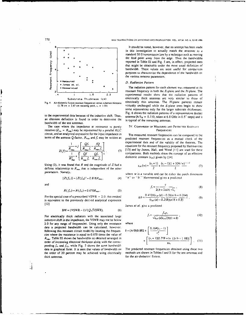
770 IEEE TRANSACTIONS ON ANTENNAS AND PROPAGATION. VOL AP-34. NO 6. JUNE 1986
6 _It should be noted, however, that no attempt has been madein this investigation to actually match the antennas to a
NX, standard 50 0 transmission line by a technique such as moving
o o the feed point away from the edge. Thus the bandwidths>"
,reported in Table III and Fig. 5 are, in effect, projected onesuc othat might be obtainable under the more usual definition of0
0bandwidth. These values are most useful for comparisonL purposes to characterize the dependence of the bandwidth on
* the various antenna parameters.
ao Measure.-d oo A D. Radiation Pattern0 A James at al.
v Homierstod The radiation pattern for each element was measured at its2 L resonant frequency in both the E-planc and the H-plane. The
4 1.6 2.2 experimental results show that the radiation patterns of
SubstrotQ Thickness (cm) electrically thick antennas are very similar to those ofFig. 4. Air-dielectric fixture resonant frequencies versus substrate thickness electrically thin antennas. The H-plane patterns remain
(1.78 cm x 2.67 cm radiating patch, i, - 1.05). virtually unchanged while the E-plane ones begin to showsome asymmetries only for the larger substrate thicknesses.Fig. 6 shows the radiation patterns of a representative thicker
to the experimental data because of the inductive shift. Thus, antenna (h/Xd = 0.110, taken at 6.8 GHz in 0.5' steps) and itan altemate definition is found in order to determine the is typical of the remaining antennas.bandwidth of the test antennas.
The case where the impedance at resonance is purely IV. COMPARISON OF MEASURED AND PREFDICTED RESONANTresistive (Z,, = R,) may be represented by a parallel RLC FREQUENCIEScircuit, and an analytical expression for the input impedance in The measured resonant frequencies can be compared to theterms of the antenna Q-factor, R,,, andf, may be written as predicted resonant frequencies as a mutual check of the
I -Qf, Rf experimental data and of the validity of the theories. The- - fQ equations for the resonant frequency proposed by Hamnerstad
R "
R ,J" (3) [13] and by James, Hall, and Wood [II] are used for theself I f RV, 1 Q3) comparisons. Both methods share the concept of an effective
- Rf, R f dielectric constant (es) given by [14)
Using (3), it was found that R and the magnitude of Z had a Ee, (w) - + (7)definite relationship to Rm,, that is independent of the other 2 2parameters. Namely, where w is a variable and can be either the patch dimension
JZ(f ,) = IZ(f,2 )f =0.818R__ (4) "a" or "b." Hammerstad gives a predicted
and Cf, i (8)R(f,I) = R(fY,2) = 0.670R_.... (5) 2(b + 2Ab) - (
For the special case of a prescribed VSWR = 2.0. this niethod Ab.=0.412
tt(c,rr (a) + 0.3)(a/h + 0.264) (9)
is equivalent to the previously derived analytical expression (cff(a)- 0.258)(a/h + 0.8)(12] James et al. give a predicted
BW = (VSWR- )/(Q4/VWR). (6)
For electrically thick radiators with the associated large f, =,____)_' )(_ 1 (10)
inductive shift in the impedance, the VSWR may not be below (a),,, (b)(l + 6)
2.0 for any range of frequencies. Using only the resistance wheredata a projected bandwidth can be calculated, however, r 0. 16
4(c,- 1)1
following this resonant circuit model by locating the frequen- 6 = (h/b)0.882+cies where the resistance is equal to 0.670 times the value of L
R.. Table III shows the bandwidths so obtained arranged in F (e,+ 1)[0.758 +In (bis+ 1.88)]1order of increasing electrical thickness along with the corres- + . (11)ponding fri and f,2, while Fig. 5 shows the same bandwidthdata in graphical form. It is seen that values of bandwidth on The predicted resonant frequencies obtained using these twothe order of 20 percent may be achieved using electrically methods are shown in Tables I and I1 for the test antennas andthick antennas, for the air-dielectric fixture.
...

CHANG e( a.: RECTANGULAR KICROSTRIP ANTENNAS 771
TABLE IlPROJECTED VALUES OF BANDWIDTH AND CORRESPONDING F, AND P F,
L a 0a
1,1Z IrS ) l
0 D
0.057 Z.ZO 2.552 3.117 a a. 7
0.047 2.834 2.952 4.093 M osured
0.061 7.632 8.152 6.607 a Jomsat ol.0 Hommrstod
0.068 4.120 4.396 6.509 E
0.094 5.632 6.140 8.699 Z .5 . , ,.0D3 .0D9 .1|5
0.110 6.494 7.272 11.441 Electrical Thickness (wovelengths)0.125 7.314 a.468 14.987 Fig. 7. Comparison of normalized antenna resonant frequencies versus
electrical thickness (h = 0.3175 cm. t, = 2.33).0.141 7.948 9.024 14.220
0.19 8.380 10.560 23.850 The predicted resonant frequencies are normalized to thezeroth order predictions and are compared to the measured,
0.166 9.442 11.560 20.660 normalized resonant frequencies. Fig. 7 shows this compari-
0.229 4.320 5.180 110 son for the nine different patches on the substrates withidentical physical thickness, while Fig. 4 shows the predictedvalues of resonant frequency for the air-dielectric fixturecompared to the actual measured values. It should be notedthat the theoretical data in Fig. 7 are presented as discrete
Z 20 0 points rather than a continuous curve so that the theory cancorrespond to the exact cases of the experimental cases, some
E of which have slightly varying values of a/b ratio and ofc dielectric constant. This use of individual points causes the
data to no longer be aligned along smooth curves. In bothlo cases it is clear that the theories follow the trend of the
U oexperimental data quite well even for electrically thick* no substrates. In fact, based on the information presented here
_ 0 Corstort Potch Size and on additional research data [15], some general observa-Constornt Sbstrote Thickress 0 tions may be made concerning these two methods. Both
0 ' predict the resonant frequency very closely for electrically thin.03 .0 .15 .20 9rectangular microstrip antennas, but as h becomes greater than
Electricol Thickness (woveengths) 0.1 Xd, James et al. give consistently better predictions thanFig. 5. Projected antenna bandwidth versus electrical thickness, the method by Hammerstad. Specifically, James et al. usually
predict values approximately 4 percent lower than the mea-
sured resonant frequency while Hammerstad predicts values-0 around 8 percent higher than the measured resonant fre-
quency. It should be noted, however, that these two theoriesare not intended for use vith electrically thick substrates. For
-n o h < 0.1 Xd, the measured resonant frequency is very nearlythe mean of the predicted resonant frequencies from the twodifferent formulas. A third algebraic formula for the resonant
9a d.9.... frequency has been proposed by Sengupta [16], but as theauthor states, it only applies to electrically thin structures anddoes not predict the proper behavior for the thicker substratesmeasured in this inve.;tigation.
-Plone, V. CONCLUSION
H-P I ... The effect of varying the electrical thickness for rectangular
microstrip antennas has been investigated experimentallyFig. 6. Antenna radiation pattern (1.1cm x 1.7 cm radiating patch. 0 3175 during the course of this research. In addition, an air-dielectric
cm substrate, e, = 2.33). model radiator has been fabricated with a single patch size and
71-) IEEE TRANSACTIONS ON ANTENNAS AND PROPAGATION, VOL. AP-34. NO. 6. JUNE 1996
a variable substrate thickness. The resonant frequency, band- coupled resonators,'' in IEEE Antennas Propagat. Soc. Int. Symp.widt, ad raiaton atten hve een easredovera rnge Dig.. 1983, pp. 67-70.
widh, nd aditio ptten hve eenmesurd oer rage 171 Hewlett Packard Appl- Note AP-22tA. pp. 5-8. June 1980.of substrate thickness from 0.03 to 0.23 of a wavelength in thc 181 W. F. Richards. J. R. Zmnecker, R. D. Ctark and S. A. Long.dielectric. "Experimental and theoreticat investigation of the inductance ussoci-
The resonant frequency of a rectangular microstrip antenna ated with a microstrip antenna feed, " Electromagn., vol. 3, pp. 327-346. 1983.
was found to decrease as a function of electrical thickness. The 191 0 M. Pozar, *Considerations for milltmeter wave printed antennas,"validity of this finding is confirmed by previously published IEEE Trans. Antenna~s Jropagat., vol. AP-3t1. pp. 740-747, t983.
results and by the existing theories of Hammerstad and of [t01 K. R. Carver and J. W. Mink. "Microstrip antenna technology."IEEE Trans. Antennas Propagat., vot. AP-29, pp. 2-24. 198t.
James et af. The predicted resonant frequencies are all very [t1) J. R. Jamses, P. S. Hall, and C. Wood. irticrost rip A ntennas-Theoryclose to the measured resonant frequency for electrically thin and Design. Stevenage. U.K.: Peter Peregrinus Ltd., 1991.
substrates. As the electrical thickness is increased, the theories 1121 A. G. tDerneryd, ''The circular sticrostrip antenna elienctit,'" in Proc.Jame etal. eneallypreict Inst. Elec. Eng. Int. Conf. Antennas Propagat., Oct. 1978, pp. 307-due to Hammerstad and to Jae la.gnrlypeit 310.
values that are approximately 8 percent high and 4 percent low 1131 E. 0. Hammerstad. "Equations for microstrip circuit dcsigs.'' inrespectively when compared to the actual values. The impe- Proc. 5l1t European Micro. Conf., Hamburg. Sept. 1975. pp. 268-
272.dance of the thicker antennas is characterized by an inductive 1141 M. V. Schneidet, "MicrOStnip dispetsion," Proc. IEEE pp. 144-146.shift in the reactance away from zero at resonance. Jan. 1972.
The projected bandwidth of the unmatched antennas was 1151 E. Chang. "An enperimental study of electrically thick rectangular
calculated to determine the effect of substrate thickness on this mirsty atnns. 19 . teiDp.Ee. .Ui.Hutncharacteristic as well. The resulting data show that bandwidths 1161 D. L. Sengupta. "Approximate expressions for the resonunt frequencyas high as 20 percent could be achieved by simply using of a rectangular patch antenna." Electron. Leif., pp. 834-835. July
electrically thick substrates. Finally, the radiation patterns of 29. 1983.
electrically thick antennas were seen to be very similar to thoseof the more usual thin ones. Overall it has been shown that Esin Chang (S'84-.M'85) was horn on Septemberelectrically thick rectangular microstrip antennas retain most 20, 1963. He eed the .S. (magna cum laude)of the desirable electrical characteristics of thinner ones and and Ivi S. degrecc n electrical cnigittce.rog front the
mayveTsit 984 anH9o rspetivey.PrHu(nmybe utilized for broad-band applications assuming a ~ UX n 19 y n of 85 H rustopectivey. Hutn
reactive network is used for impedance matching. He was employed by Schlumberger Well Scrv-es in Hoston, TX and was involvedl in the
REPEENCF ~sengin eerng %ippmi of clectromneovrc propagationIl I I.Scsnhrt.P I.PrEFrr.A.tSnsti u-1, lir Z b o woc E a, a' A li duotc Research and
111 , I. Sl):utx(, FG. arrr, . I Sin-isandS 1 IlyeTeahin &sao at the tlniversitv of Houston i''Microstrip antennas with frequency agility and polarization diyer- the area of applied elecicomagnetics while complet-sisy.'' IEEE Trans. Antennas Propagat.. vol. AP-29. pp. 118-123. ing the M S. degree. He is cxrrend tlh etlced as an Enpircc; "cit Shell Oilt991. Company in cotmunications in Houston. TX His primaty inteccs are in
121 S. A. Long and M. D. Walton. ''A dual-freqaency stacked circular- microstrip antenna Icebsology. high speed telccommttiovt'. 'i dcit!disk antenna. IEEE Trans. Antennas Propagat.. vol. AP-2't. pp. telephony.
1270-273, 1979. Mr. Chang isa member of Eta Kappa Na. the'rTevas Society M' l'rofemoinal131 W. F. Richards, S. E. Davidson. and S. A. Long. ''Dual-band Engineers. and M A L.S
reactively loaded microstrip antenna." IEEE Trans. Antennns Propn'got., not. AP-33. pp. 556-561. 1985.
141 A. Sabban, ''A new hroadhand stacked twso-layer mtcrostrtp antenna." Stuart A. Long (S'65S'72-M'74.5M 80), for a photograph anti biographyin IEEE Antenna Propagat. Soc. Int. Symp. Digest, 1983 pp. 63- pes e ae51o h a 95iseo hsT_\SCIN
[1K. F Lee, K. Y. Ho. and J. S. Dahele, "Circular'disk microstripantenina with an air gap." IEEE Trans. Antennas Propagat.. vol. AP-32. pp. 80-884, 198.1. William F.~ Richards IS'69-M'70-Xf'R01. for aphoworaPh and biography
161 0. Kumar and K. C. Gupta. "Broadband microstrip antennas using please see page 561 of thc May 1985 issxe of this TRsNSACTlON'.

DPENI E - X CIEEE Antennus and Propagation Society Newsletter, October 1986
Reactively Loaded Microstrip Antennas
William F. RichardsStuart A. Long
Department of Electrical EngineeringUniversity of Houston - University Park
Houston, Texas 77004
1 Introduction 2. The quality factor of the micros'rip element can be determinedwith good accuracy using the resonant cavity field rather thanthe exact antenna field. Once the quality factor Q is deter-
Microstrip elements have proven to be very versatile and have found mined, an artificially lossy dielectric with a loss tangent equaluses in a variety of applications from satellite arrays to automobile to the recprocal of Q can be imagined to be filling the cavity.anti-collision warning systems. This versatility stems mainly from The field within sl a cavity approimates the field between
their structural simplicity, ease of construction, ruggedness, con- the patch and ground plane of the original antenna.
formability, low profile, and low cost. In addition to these features,
microstrip elements are capable of producing a variety of different Thus, the most fundamental step in determining the properties of
patterns and polarizations [1], [2), [3], [4), 15], (6], [7), [8). Most a loaded antenna is to determine the resonant frequency and moderesearch efforts, however, have been limited to basic applications distribution within the corresponding loaded cavity.using only a single, unperturbed mode of a rectangular or circu-lar element. Additional applications are possible through the use If the reactive load is imagined as being contained within a smallof reactive loading. These include multiband, frequency-agile and cylinder extending between the ground plane and the patch, thenpolarization-diverse, adaptable-impedance and multimode-pattern lfuygen's principle can be used to replace the load by equivalentantennas. Some experimental work has been done in these areas [2], magnetic and electric surface currents impressed in a now empty ca-(3], [4], but very little theoretical work with the exception of [3], [5], ity. Since microstrip elements are thin, the magnetic sc-race current[7], (8], [9], [10] has been done. In this paper, a very simple theory is is primarily a horizontal circulating loop of current and the electricpresented which will guide a designer who wishes to take advantage surface current is vertically directed. By making suitable transforula-of the added flexibilitv that reactive loading provides. In additi., tions [13], one can approximate the field due to the magnetic currentseveral applications are discussed with corresponding theoretical and as a constant times the field produced by the electric current actingexperimental results. alone [10]. The effect of the equivalent magnetic current is usually
negligible anyway and thus the effect of the load can be accountedfor by impressing an equivalent electric current on the surface of
2 Theory the small cylinder enclosing the load in an empty cavity. The totalequivalent current is just the total load current IL.
A simple theory that makes use of a graphical interpretation of thecharacteristic equation for the resonant frequency of a loaded mi- Characteristic equation for the resonant frequency- There
crostrip element is presented in this section. By a "reactively loaded are two expressions for the load voltage that one can write which
element" we mean a simple microstrip antenna to which one or more, when equated, yield the characteristic equation for the resonant fre-
two-terminal lumped, lossless, linear load impedances are attached- quency of the loaded cavity. One expression is that the load voltage
one terminal to the patch and the other to the ground plane. Also Vji is the driving-point impedance of the empty cavity jXl times
included in the set of reactive loads are sections of transmission lines the load current I., where X1 is the driving-point reactance. The
attached at one or more points on the patch. The simplest form of second expression is the defining relationship for the load itself,
tile theory results when the original, unloaded antenna has one ofthe separable shapes which fall into four classes: rectangular, circu- YL = -JXL[L,
lar, elliptical, and parabolic. In this paper, we will deal only withrectangular elements, where Xt, is the load reactance. Combining these two equations
yields the characteristic equation,Fou ndation--the cavity model- Tire fo,-rtirron urpon whichtile theory is built is the so-called cavity model [11] as modified in XL, + Xrr = 0.[12]. This model is best suited for understanding loaded elementsbecause it cal reconstruct tire localized field inl the vicinity of the A very useful graphical inte pretation of this characteristic ciuationloads, yet it is simple enough that basic physical principles useful in can be obtained if the microstrip cavity is modeled as seen fromdesign can be developed and is also surprisingly accurate. It is based the loid terminal pair as illustrated in Fig. 1. The resonant circuitor two observations. shown ill tile figure represents the contribution to the driving-point
impedance froi tile resonant mode of the empty cavity whoe res-I1,h rvtl par,!;, t i.t of tile r :,nt r.,"j r . a n,,,riarstri, -t ' ;rrilr.-nnrt In;at
it ftcr1 ,iiv * % s i ;ire- t Ithat of tle corrsponding loaded cavity
is alrproxirratey tine san, u.s that of a cavity f~lrrrlt-r hy iiLtron rnde of istorr-st. flh reactive :ontribution dur to all other modesluring a ssagretic condrctor Iretwvc tire patch edg d tiny of tire errpty cavity in the loster expansion of the driving-point
ground plane impedance is whit wc call the "feed reactance," X . We have de-
1

IEEE Artnn. il P,.pogotin Soutety N-mIft-e, October 1986
xf
r XrI
I c ILL - --
Figure 1. Circuit model ror the input impedance of a microsteip cavity. 'X L
Frequencypitted this an a simple inductive reactance althoughr it does not re-ally correspond to a. single inductor. In most cases, particularly canesin wvhicht degenerate- or nearly degenerate-teode pairs of the empty.
advity (io trot exist, Ilac feed reactance is inrdceed ' osi Liv iaend slowalyvarying over the band of both the loaded-cavity and empty-cavity X,modes of interest. Regardless of ltow it is depicted, it is computedusittg thre full modal analysis of thre cavity arid an such.- it is precise.2Using thIs model, tire characteristic equation becomses
(1L + -f) =____.
An es-en simspler may to obtain this claiurcteristic equationt is to apply2Kirchoff's voltage lane to the circuit illustrated in Pig. I reith thre load -Xreactance attached. Sirce a resonant tmode of thre loaded element is/a source-free mode, the srrrr of thne voltage drops aroundir thre loop _______________
must vatnish implyirrg that Frequency
(X~ +A1 +X,)1t= ~.Figure 2. (a) Plot of Ar- -(Xj + XL) versus frequency; (b) Plot of Xe, - Xf(XL +Xf +X,)I = 0for three different feed locations.
This yields the characteristic equation (I) since It, rmust nut Ito zero.
In order to develop import!ant design concepts, it is useful to solve This obsetvation illustrates hose load placensent affects the res-equation (1) graphically. Such a graphical solution is illustrated in ovans frequrency-. A short placed rear the centerline changesFig. 2(a). The simple case a short-circuit load X, = 0 is consid- the resonant frequency little. As the load is moved awaay fromered first. The intersections of thne danhed line in Fig. 2, representing the centerline in either direction tossurd an edge the resosutit-Xf alone, swith the solid line representing Xr marks ltne rc-rttstt frequerrcy inrcreases rapidlly at first and thren nmore slorvlr as thefrequency of the loaded cavity load point nears thre edge.
Several design principles emerge from this figure. particuilar)y in ref- This graphical interpretation, wehich wvill be found very usefulerence to the rectangular element illustrated in Fig. 3. in later applications, is consistent wvith the observation that
the load will have more effect on the resonant frequency wehen
1. It is immediately cleat tirat thre introdluction of a short Circuit placed wehere the empty-cuelty field is strongest and no offect
will increane the resonant frequency of the ravity. wnhere tire cavity field is zero.
2. The resonant reactance corresponditng say to thre flu = 01 nt =I
mode of the rectangular element (thre mode rost crirmorly
usd s 2c' cost(ny/b) Feed point 3
oh = r)W - ct
- (2)
wnhere the patch dimnisions are a x b xe I, c is thre spreed of lightin the coetpt dielectric, ko0, r/li is thre rsonrant'veirnner of the (0. 1)- rine, and y is thre y coordinsate of lthe loadposition. Whten p approachres either edge, yp 0 or y =t,sthe resonrant reactaince given itt eqinatisri (2) b-ynttu- statiir.,try. As y -- h/2, tire ressurunit rerictnce aprproachtes veto It jrced point 2grapictal termrs, sthe reactansce curve breginis as a very s'ittler Feed po01nt 1deprarture. frmr zero for loard points tlear v - b/I? itrilhn las-tens out an p mroves au-ny Iiusi thre content tie For loadl loot 1near the edge, the A', curse chtannges little- This trenrd is 1tus-trated is Fig. 2(b) 1,ry the 'eenrne cf three AX it .. es. labteled
1 -3 correspontding to feed points 1 -3. Figure 3. Rectangurlar element wish three ditferent loud locations.
IEEE Antennas and Propagation Soclety Newsletter, October 1986
3. The preceding observation about the dependency of resonant unnormalized mode function i(r) of the loaded cauity in terms offrequency on load position made the tacit assumption that the the modes of the empty cavity isfeed reactance is independent of of feed position. Nothing couldbe further from the truth. In fact, the feed reactance can vary = " " r) 3)by a factor of three or more as the feed point is inoved from .A V-- ,L.3)place to place on the patch [131. The feed reactance typicallyincreases as the feed point is moved near an edge. The increase where k is the resonant wavenumbef of the resonant mode of theis rapid when the feed point is very near the edge. This feed loaded cavity and r, is the position vector for locating the center ofreactance is predicted fairly well by the cavity model, particu- the load. No integration is used in this expression since it is not usedlarly for thinner elements, except for feed points right on the to compute the field in the region of the source (i.c., load) current.edge. There, the cavity model substantially overestimates the The evaluation of this series is also facilitated by the use of an SEMfeed reactance because the equivalent electric currents on the expansion with a quasistatic correction.magnetic wall that would make the cavity model precise havebeen neglected. These equivalent currents tend to oppose the It is apparent from equation (3) that the closer that the resonantimpressed source current (in this application, the load current) wavenumber k is to a given k, associated with a particular mode ofand ignoring them results in an increased inductive reactance, the empty cavity, the closer the loaded-cavity mode will resemble the
The effect of this variation is that as the load point moves 0_(r) empty. cavity mode. More will be said about this for specifictoward the edge, the -X curve moves downward. This is il- applications discussed in the next section.lustrated by the sequence of three curves in Fig. 2(b). Thus, Quality factor, pattern, and impedance- Once the modal dis-it is expected that the resonant frequency should begin at the tribution has been obtained, the pattern can be approximated as theresonant frequency of the empty cavity when y is on the cen- field due to a filamentary magnetic loop of current coinciding withterline, it should increase rapidly at first due to a widening Xr the edge of the patch. The current at a given point r on the loopcurve, and finally decrease somewhat due to a rapidly increas- is i'T(r) and is impressed over a grounded dielectric slab with theing feed reactance for load points near the edge. This is, in patch removed. Once the pattern is obtained, the power radiated infact, exactly what is observed by measurements, the space and surface waves can be computed. The average energy
stored in the electric field is computed using
Determination of feed reactance- In order to graph the -X s
curve, the input reactance of a microstrip cavity must be computed. 1 23 3-W _v(Ct)This can be obtained by using the Green's function, wW, = 2te p'kr , (k
2 - k
2,)2 + 5WL,
G 3su) = . -ij .Z - --i s .VWhere W', is tile average electric energy stored by the load. From theA k - k2, radiated power Pr and the stored electric energy W,, the radiative
quality factorwhere A is the set of all pairs of non-negative integers, (rn,n), andvf,_(r) is the mn'
5 mode of the cavity satisfying 4v fnW.
Q1 Pr) E S, is computed where Jo is the resonant frequency of the loaded an-
tenna. In addition to the radiative quality factor, the quality factorss's(r) • A = 0, r E 8S. associated with the power consumed in heating the dielectric and
metal cladding are Qd = 1/6 and Qn, = t/A, where 6 is the actualThe source and observation position vectors are r = z:i + y , and loss tangent of antenna dielectric, and A is the skin depth in ther' = z'"; + y'j, S is the set of points making up the patch, 8S is the metal cladding. From these quality factors, the quality factor of theset of points on the patch edge, and ii is the outward-pointing unit antenna is determined usingnormal to the patch edge. In the case of rectangular elements,
Q= + + ..2 Con (mrnz) Con'Qyt
To compute the input impedance (at least for the case of loaded
The series for G(rlr') diverges as r - r'. This is because the in- elements in which only one resonant mode contributes significantlyThe eris fr Grlr) dveres s 5- r. hisis secusethein. in the band of interest), one can use thle circuit model illustrated inductive reactance associated with a filament is infinite. In order to in The ad i n e res onan t Circuit o s
obtain the input reactance associated with the actual load current,one must integrate this Green's function over the load current distri-bution. It is assumed that the load current is distributed uniformly Yr = G [I + jQ((LV -1l].on a circular cylinder of diameter d. The "location" of the load is , I)the center of the cylinder's cross section. The required integrationneeds to be computed efficiently since the nonlinear characteristic The conductance G can be determined by using the relationequation for the resonant frequency must be solved numerically, orenough points plotted to solve it graphically. A very efficient SEMexpansion of the cavity field with a quasistatic correction has beer 1tl'fG
= P,
developed [10, the details of Which are too lengthy for presentationhere. Once thy integration has been carried out, the result, when where voltage V, across the resonant circuit isimultiplied by -jr yields tile total reactance V, It tile load pi'itfrom whichi thyeresonutnt reactance call be sibtracted le;viing Xr. V, = -19P(rr),
Determination of the modal distribution- Once the resonantfrequency is deternined, the task turns to computing tile modal dis- r being tile location of the feed of the loaded element. The powertribution of the loaded cavity. For the case of a single load, the P is the total power absorbed by the antenna element corresponding
13
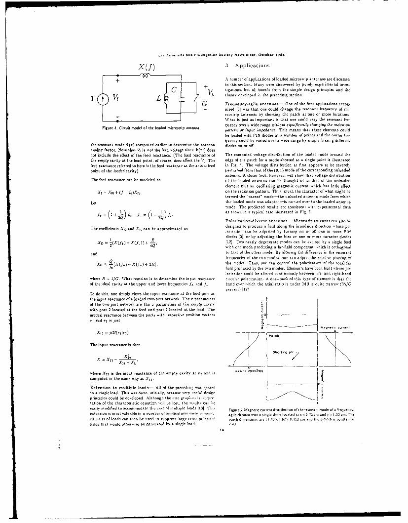
,.a Mli~rtoa asona Pr-pogotion Society Newsietter. October 1986
X(f) 3 Applications
+A number of applications of loaded microstrip antennas are discussed
+ in this section. Many were discovered by purely experimental inves-tigations, but all benefit from the simple design principles and the
Vf V theory developed in the preceding section.
(G Frequency-agile antennas- One of the first applications recog.-- uized [3] was that one could change the resonant frequency of mi.
ciostrip antennas by shorting the patch at one or more locations
What is just as important is that one could vary the resonant fre-
quency over a wide range without significantly changing tie radiationpattern or input impedance. This means that these elements couldbe loaded with PIN diodes at a number of points and the center frequency could be varied over a wide range by simply biasing different
the resonant mode 'I(r) computed earlier to determine the antenna diodes on or off.quality factor. Note that V is not the feed voltage since Y(rt) doesnot include the effect of the feed reactance. (The feed reactance of The computed voltage distribution of the loaded node around titethe empty cavity at the load point, of course, does affect the Vi. The edge of the patch for a mode shorted at a single point is illustratedfeed reactance referred to here is the feed reactance at the actual feed in Fig. 5. The voltage distribution at first appears to be severelypoint of the loaded cavity), perturbed from that of the (0, 1) mode of the corresponding unloaded
atntenna- A closer look, however, wvill siote% that voltage distributiontThe feed reactance can be modeled as of the loaded antenna can be thought of a.s that of the unloaded
element plus an oscillating magnetic current whicli has little effect
Xt = Xro + ( - fo)Xn. on the radiation pattern. Thus, much the character of what might betermed the "parent" mode-the unloaded antenna mode from which
Let the loaded mode was adapted-is carried over to the loaded antennaniode. The predicted results are consistent witl experimental data
f+= (l+l-)fo, j-= (i--)fo. as showvn in a typical case illustrated in Fig 6.Polarization-diverse antennas- Microstrip antennas can also be
The coefficients Xio and X, can be approximated as designed to produce a field along the broadside direction "hose po-larization can be adjusted by turning on or off one or more PINdiodes [3], or by adjusting the bias on one or more varactor diodes
R[(x +) + X(f) + [12]. Two nearly degenerate modes can be excited by a single feed2 ) X ) +--,with one mode producing a far-field component which is orthogonal
and to that of the other mode. By altering the difference in the resonantfrequencies of the two modes, one can adjust the relative phasing of
Tr - [X(f+) - X(f_) + 2R], the modes. Thus, one can control the polarization of the total farJo field produced by the two modes. Elements have been built whose po-
larization could be altered continuously between left- and right.handwhere R = 11G. What remains is to determine the input reactance circular polarization. A drawback of this type of element is that theof the ideal cavity at the upper and lower frequencies f+ and f- band over which the axial ratio is under 3dB is quite narrow (35/Q
percent) [12.To do this, one simply views the input reactance at the feed port asthe input reactance of a loaded two-port network. The z parametersof the two-port network are the z parameters of the empty cavitywith port 2 located at the feed and port 1 located at the load. The
mutual reactance between the ports with respective position vectors ari and r 2 is just
magnetic current
Xt2 = jtG(-lit2) Patc.h 0
The input reactance is then
Shring pinX 2
X =X225 - t12
where X 21 is the input reactance of the empty cavity at r2 and is usd00 oiau5t icomputed in the same way as Xt.
jcExtension to multiple loads- All of the preceding was gearedto a single load. This was done, initially, because very iiscitil design ;
principles could be developed. Although the nice graphic; I ilterire-tation of the characteristic equation will be lost, the results can heeasily modified to accommodate the case of multiple loads [10] fhs Figure 5. Magnetic current distribution of the resonant mode of a frequency.
extension is most valuable in a number of applications since svmriiv: agile element with a single short located at x= 5.72 cm and y = 1.52 cm. The
ic pairs of loads can thens be used to suppress large cross- laiizmd patch dimensions are 11 43 X 7.62 x 0.152 cm and the dielectric constant isfields that would otherwise be generated by a single load. 2 43
14

NEE Anfonna. and Propagation Society Nesultatter, Octobr 1986
. " - --i ... . " -. S h o rt- W -
.. ' . "' .. circuit 7
, 1335 MHz
Short at y= 1.52c .\
( s ).....................Oo, Figure 7. A monolithic dual-band element using a short-circuited transmis-
.. .-...- sion line recessed into the patch.o//
a large grounded dielectric slab, the patter-_ (&Us off to zero in anydirection parallel to the patch. If the dielectric is truncated at the
patch edge, the gain also falls, but not to zero. For the purposesa-o Measured of the present discussion, we will assume that the dielectric is so
o o Computed tntricted Another mode of a nonloaded microstrip antenna is theDC .uode-a mode resonant at zero frequency which has a constant
5 M-lz increment voltage distribution from point to point on the patch. If this mode
Figure 6. Input impedance of a frequency-agile element described in Fig. 5 could be excited at an RLF frequency, the pattern it would produce iswith the feed point is st (2.54, 1.27). basically the same as that of an electric monopole element mounted
perpendicular to the ground plane. This yields a pattern which hasa broadside null and a. maxaum along tb gsTond plane. The first
Dual-band elements- In some applications, two or more rather question to be addressed is how to resonate this mode at a usefulnarrow, discrete frequency band. of operation are often required with frequency instead of at DC.band separations of only a few percent. One technique that has beenused is to stack el-ments of different sizes [141, 15). C ne experimental To answer this question, we consider the DC mode to be a parentresult using a reactive load was reported in [2J. The present theory mode and plot its corresponding Xr and -Xt curves as illustratedshows the type of load that is needed and how to control the band in Fig. 9. It turns out that if XL = 0, the resonant frequency (oc-reparation. curring where the dashed curve and the X, curve intersect in Fig. 9)
is still a little too low to be useful. To raise the frequency evenFigure 2(a) illustrates the uses of a load reactance which has a pole higher, an appropriate amount of capacitance can be added. If thelower than the resonant frequency of the empty cavity resonant par- load capacitor is placed in the center of the square patch, then theent mode. If a.dusted popteTly, two intetsections between the Xr resonant frequencies of the (0, 1) and (1,0) modes of the antenna arecurve and the -(Xr + XL) curve occur corresponding to two daugh- unaffected and all three modes can be made to resonate at the sameter resonant modes of the loaded cavity. The band separation can frequency, An alternative to using a capacitive load is to use fourbe controlled in two ways. short circuits as illustrated in Fig. 10. The voltage distribution along
I. If the magnitude of the slope of the -(Xr + XL) curve is in-creased, the bard separation is reduced.
2. If the load is placed closer to a zero of the parent mode function,then the Xr curve becomes thinner again redurcing the hand/separation. /
Of these two methods, the latter is the easiest to implement. The - -resonant load can be simply an open- or a short-circuited transmis-sion line, which can be etched on the same plane as the patch itself.III this case, the patch may need to be slotted and the line recessed \
as illustrated in Fig. 7 in order to control the band separation and
still maintain at least bilateral symmetry in the element to reducecross polarization. . . . . . .
It is clear from Fig. 2(a) that there is a contiinots set of possiblepairs o f d ual reso n ant frequ....ies o b tai nable by va ry ing th reso na n..t -" " - £ z ' v "/
frequency of the load. However, it turns out that there is really only - ione pair of resonant frequencies which yields resonant modes whose xinput impedances are approximately tire name. For all other pairs, -.the rIraximiu lU input rsistance of one is larger than the threr. II
,xtr ;t , s t ' i ti,, h S ,t -p " y ti,:it -1l' d that it i , 2.50 C "t 7 /
ligare 8 contains the treasured input impedance of both ootles of a " INCREMEN' to MHZ /typical rual-hand clement ./
DC mode applications- IiI all of the applications discussed above,lIe parent mode used almost exclusively was the (0, 1) mode of arectangular clement. This mode produces a pattern with a beam Figure 8. Measued input impedances of both modes of a typical dual-bandS itaxitiuttn in a dir-ction perpendicular to the patch If mounted on element using a shorted transmission line as its resonant load.
15
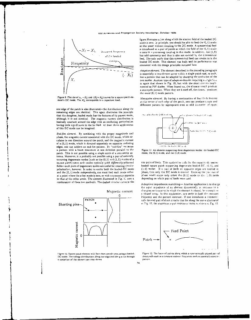
lahs Antennoas and Propagation Society Newsletter, October 1986
figure illustrates a line along which the electric field of the loaded-DCmode is zero. In principle, one should be able to feed the 10, 1) mode
at that point without coupling to the DC mode. A symmetrical feed
V -is introduced at a pair of points at which the field of the 10, 1) mode- l ,Itlnrt r ,tw. y is zero th. preventing coupling to this mode. In additic, _. the (1,0)
if 0,cloadedhas odd symmetry and thus is also not excited by the s;'.mmetrical)feed. The only mode that this symmetrical feed can coup!e to is the
C c.,I y loaded DC mode. This element vas built and its perfornance sas
consistent with the design principles outlined here.
0) - - _ Adaptive element. The element described in the preceding paragraph( X ') is essentially a two-element array within a single patch and, an such,
has a pattern that can be adapted by changing the excitation of thetwo modes. Auothet type of adaptive element requiriug a _z e fc,-
is again that shown in Fig. 10, but with the short circr-its imple-
mented as PIN diodes. When biased on, the element w-oLd produce
a monopole pattern. When they are biased off, tie eleiiie produces
the usual (0,1) mode pattern.
Figure 9. Plot the ofx,, -Xf. and -(Xf+XL) curves for a square patch ele- dfonopulse clement. By having a combination of four fte-Js locatedintu's DC mode. The XL corresponds to a capacitive load.
at the center of each edge of the patch, one can produce a sum anddifference pattern by appropriate even or odd excitatio- of oppo-
one edge of the patch is also illustrated-the distributions along theremaining edges are identical. This again illustrates the principle
that the daughter, loaded mode has the features of its parent mode, ,,l.,l i ., (l . ,...,l .,,,,,. fI-, k,,.,I- ... k,,,,I,
although it is not identical. The magnetic current distribution isbasically constant around the edge with an oscillating perturbation o " 1,,,,, ul -
having little significance in the far field. At least three applications .- ...
of this DC mode can be imagined. . -.. .. .. .. ...
End-fire element. By combining with the proper magnitude andphase, the magnetic current associated with the DC mode, which cir-culates in one direction around the patch, and the magnetic current
of a (0, 1) mode, which is directed oppositely on opposite radiatingedges, one can achieve an end-fire pattern. By "end-fire" Ave mean U.I t, , I.,,. ,
a pattern with a beam maximum in one direction parallel to the Figure II. An element supporting three degenerate modes: the loaded-DC
patch. This is not possible using a single mode of a microstrip an- mode, the (0,) mode, and the (1.0) modetenna. Moreover, it is probably not possible using a pair of naturally
occurring degenerate modes (such as the (0,1) and (1,0) modes of asquare patch) since such modes typically yield differently polarized site pa;rs of feeds. This application calls for the capacitiv-nly center-
fields-such pairs of degenerate modes are useful for creating circular loaded square patch supporting degenerate loaded-DC. - 0. 1), and
polarization, however. In order to excite both the loaded-DC mode (1,0) modes. If a pair of feeds on opposite edges are excited inand the (0,1) mode independently, one must feed each mode either phase, then only the DC mode is excited Exciting the ajr out ofat a point where the other mode is zero, or with a symmetry opposite phase would excite only either the (0.1) mode or the 1.0) modeto that of the other mode. The element illustrated in Fig. 11 uses a depending on which pair of feeds were used.
combination of these two methods. The dashed circular curve in theAdaptive impedance niatching- Another application is to change
the input impedance of an element dynamically in response to a
M agnetic cttrrcn t h -lging evi ..tet. t. n t in hich the elette t is pl ce , for , tn.cal e lla phased array. In this application, one seeks to hold the resonant
0 - frequency and the pattern coostant. If one introduces a zymmetri-
PATCH cally located pair of short circuits that he along the curve illustratcd
. in Fig. 12. the maximum i put resistatice i-aries as shown i Fig 13.Ir
---S h.r....... .---
Feed Point0\Patch X
I'igtr 10. Square patch element with four short circuits procueing a loaded- Figurre 12. The locs of points along which a symmetrically placed pair ofDC mode. lre voltage distributions a-long one edge iand alotg a cut through shorts will result in a constant resonant frequency and an essentially constanta centerline of the eleenent are also shown pattert.
16

IEEE Antennas and Propagation Scclety Newsletter, October 1986
200 of reactive loads can be used to control the resonant frequency, po-larization, impedance, and radiation pattern. These characteristicscan then be made electronically adaptable to various systems needsif the loads are PIN or varactor diodes.
0
a100-References
[1] John Huang, "Circularly polarized conical patterns from circularmicrostrip antennas,"IEEE Trans. Antennas Propagat., vol. AP-32, pp. 991-994, Sept. 1984.
0- (2) J1 Krr, "Microstrip a etla devcopmnte," Froceeding of the
0.00 2.00 4.00 6.00 Workshop on Printed-Circuit Antenna Technology, Las Cruces,
* z-component of short-circuit location NM, pp. 31-3.20, Oct. 1979.
Figure 13. Variation of the maximum input resistance as the load pair is [3] D.H. Schaubert, F.G. Farrar, A.R. Sindoris, and S.T. Hayes,moved along the curves illustrated in Fig. 12. "Microstrip antennas with frequency agility and polarization
diversity," IEEE Trans. Antennas Propogat., vol. AP-29, pp.118-123, Jan. 1981.
Pattern shaping- There is not a lot of shaping of the pattern thatone can do with a microstrip element since it is not electrically large (4] B.F. Wang and Y.T. Lo, "Microstrip antennas for dual-
and the magnetic current distribution must be essentially real-valued, frequency operation," IEEE Trans. Antennas Propaogat., vol.However, one can, in principle, obtain a more nearly isotropic pattern AP-32, pp. 938-943, Sept. 1984.in the E-plane by ,ppropriately loading one edge of the element.(Again, the dielectric must be truncated at the edge of the patch). [5] W.F. Richards, S.E. Davidson, and S.A. Long, "Dual band,
The concept in this application is to place loads at one edge so that reactively loaded microstrip antenna," IEEE Trans. Antennas
the net magnetic current at that edge is zero as illustrated in Fig. 14. Propagat., vol. AP-33, pp. 556-561, May 1985.
The magnetic current at the opposite edge is not zero resulting in a [6] S.E. Davidson, S.A. Long, and W.F. Richards, "Dual-band mi-single magnetic dipole for this pair of edges. There is a net magnetic crostrip antennas with monolithic reactive loading," Electronics
dipole on the remaining pair of edges, but they do not contribute Letters, vol. 21, no. 20, pp. 936-937, Sept. 26, 1985.any field in the E-plane and their maximum field strength in the H-plane has been computed to be down by about 9dB from the main [7) W.F. Richards and S.A. Long, "Pattern adaptation using
beam. This yields the desired isotropic pattern. Some shaping of loaded, dual-mode microstrip antennas," IEEE Antennas Prop-
this pattern is possible by adjusting the net magnetic current at the agat. Symposium Digest, Vancouver, BC, pp. 93-96, June 1985.
loaded edge. (8] W.F. Richards and S.A. Long, "Matching micrstrip antennas
using reactive loads," IEEE Antennas Propagal. Symposium Di-
gest, Philadelphia, PA, pp. 431-434, June 1986.4 Conclusions (9] D-L. Sengupta, "Analysis of tunable rectangular patch anten-
nas," IEEE Antennas Prpogat. Symposium Digest, Boston,The basic theory of loaded microstrip antennas and numerous prac- MA, pp. 267-270, June 1984.tical applications have been discussed. Proper selection and location [10] W..Richards and Y.T. Lo, 'Theoretical and experimental in-
vestigation of a microstrip radiator with multiple lumped linearloads," Electromagnetic.. vol 4, no. 3-4, pp. 371-385, Sept. 1983.
(11] Y.T. Lo, D. Solomon, and W.F. Richards, "Theory and exper-iment on microstrip antennas", IEEE Trans. Antennas Propu-gal., vol. AP-27, pp. 137-145, Mar. 1979.
[12] W.F. Richards, Y.T. Lo, and D.D. Harrison, "An improved the-
ory for microstrip antennas and applications," IEEE Trans. An-tennas Propogat., vol. AP-29, pp. 38-46, Jan. 1981.
[13] WE. Richards, J.R. Zinecker, R.D. Clark, and S.A. Long, "Ex-perin.ental and theoretical investigation of the inductance asso-ciated with a microstrip antenna feed," Electromagnetics, vol.4, no. 3-4, pp. 327-346, Sept. 1983.
[14] J.S. Daliele, K.F. Lee, and P.Y. Lee, "Experimental study ofthe characteristics of coupled top-loaded microstrip monopoles,"IEEE Trans. Antennas Propogut., vol. AP-31, pp. 530-531, May1983.
Figure 4. Voltage distribution along the edge of a rectangular patch loaded 1151 S .-\ loiig and M D Walton, "A dual-frequency stacked
with a pair ofcapacitors. The net magnetic current on one edge is zero, but circular-disk antenna," IEEE Trans Anlennas Propgnl.,
is not zero dn the other. vol. A P-27, pp. 270-273, 1979.
17

OE~o.n,, 0 ... if ~i~a' £tt ta>..vZ .- SSV~t C-~~~c -0a~ .C~ '
v.~ E . .o~a . z0
0a tv 0 . -0 T F
c Z0NE 0 3 5 £ vV O c 4JLE00- LU . v _0~V 3... _.ccA 0 C -0> z
S c CU D 0- vL Kt. > aaao0 v : 2M.,.> Co0 %.C.- 0 L >
v.3c-- c0- a ~ .I' " , 4v
>C u v C 'o a 'gO.
o vo£ LV
-Z 0~ 1a R
L 0
a - Va.-
5c .5 s'mV v£,. o2 ~ cV o
-,1 'o. a0
or VO Q .0c w. OP .
0-C 5
C..Z - U.2 5
CC Ls ct.v&0 8 fO 0
aU-Z o~U~ ~ S V
£O V u~ 00 vL. '5
VQ LO C , '-C -s 5 '0 A, 0Cmv --LV L U . - aSv ~ 0 t U .. ~ % i
"-OOO £.-c
0-1SC U
L c a-0 0
'.4 ' c
.<~X o -a;o
a 0 m LJ>o ~W C ~ >Caa~o
ZO -! 1U - - -'- LU-
v -ut; U01U4L 'a
Or, V-eMe
E g 2'z- f0 m
II
I-~ ~ 330 5 S.a 0
.. UV
.2--0 14U 0 x C C

0 c v m 0 V4 -"- C C- .0-mI00 C 1 . - X) 0 C -)V
0 .2.4 . I L -. f 4) C)
0 R. 40.04
1 a0 c
a- 0L 0..- v
a-O u
2 ' E0 N. *' C 0 t)~ '.*I .. 0 w 0
4)L0 g. p )
~~.0- 02 1.~va0
C'
.o Z4)
4- Zz~ lu 10O0 4z
0 C L .4 0 c 0 .- t0- -004 -0 .0 N.,..0Q0 ,u- ao 0,
a'--o'-aa~ua C- O*-ou,. N A.
to 1/

-- a
ot o~C a) .CSIA
0f0 -c QV 3
C~- -- ..c .0.1 U - ,C
0 V!a1 AIWV
if C 6g 0 C 01.3a
r t, - a o
CC
- Z -5V
C C, v 3- - c2o So C4t, V- - V
L -ec 2 -'-
ZV Mc V Vow
o~~ mOj "vf
3L V; .2c o,. a
c ao
CVo 3 az, - m .
2- - V
U)) C Vt
C.2 .. '..... V
- a t,-a C 'o.,V '
Uc 3 o ot t.2 t M, ; .
ta 3 tE o ~ RE a x X. e
* a o a-VE x c meE o
o CCe. *C0QV- .Loa 3 o w.'c
oa M o L o CC
W0
Z~ .. a-C U -a" V
o2 Ct, g L t, u, VO f V
a.o moC
E *5. as aa. . Vo Ie C aa u
c c2.& o o ~~0V , V a ow SW- - q6
£~~~~~ -,2 -a C V a
Vta- C' c 4C 00 T' v C V .V-.1 ol U ~V
o v cn,.taC> ou w o. > at,

.,2- -0 .0 -0..0C O V0
0 o~ CL ~ Q
t ~ 0 ~ .0 Sm. ' o.< .
t St t . 0 C. .. ~o0
0'- 0 v -a 0
a o .0 m a- m I0"
> So. 0 a"0 ~ LN
wm x0
0 o
I-
c , C L u m0 10L. so0 ~ I~
oI -. 0-
0 0 "30

- LL
x -
Kn
0 ,'
enn
0. 2
mv a fNO * v u uw c .
c 0 - -. ,
0 u
* CY.
u
o, CU, 0
C
oo - C
otoc~~~ -0,- ~ ov ~ ,0- -CU, K K 4
0 CZ - '
7A 0 c A m U~ L ) 4) c1k ' a'cvo E
4 L .- > a 0 ,
3. U C

N0
NN~' Al:
x ) Ix ~ a x
IC aa N x
xC x.~ .
xxx
CD wC 81 Xa
x a
4144
A C.
A C.
7 x * x -
is~ ~ LU r
II
U
Nx x
Xx~~ x6~
8 xX
xx g
x- 0
19 I 0N
-x ax a
'-'-C.
IC LII
x N 0X x x8
8 6 8 : Cx x x
XXI an (2.', Il x
xN 0x
'--C 0
XB x-
0 Ixi 0
Ir-

j0, - 0 440 440 0 ~ 0
X cE - g 0 6 - 4'
0-- Cl
- 31~ 0 " 4 .40(44,4' I
Cr > )L
4,-~~~ 0 0, 4C
I~ 44
~~eo2.4 ~~~ ~ 0 'T05~' g *0 ' ,YC I
-~~~~S '0C C '- '
4'N OD.0

IEEE TRANSACTIONS ON ANTENNAS AND PROPAGATION. vIP'. I DECEMBER 1960 1467
Ali Asymptotic Extraction Technique for EvaluatingSommerfeld-Type Integrals
DAVID R JACKSON, MEMBER. IEEE. AND
NICb)LAOS G ALEXOPOULOS, SENIOR MEMarER. IEEE
Abstrac -Aii asyr poli it rIC1io1 process is developed whit? leads
to an efficient method foi the evaluation of (he electric field from a
Manuscript received f-cbroar) 11 ;986. revised May 27. ]986. This workwas supported under U S. Aria Research Coltracis DAAG 29-83-K-0067nd DAAG-29-&4.K-OI6-), R J.ckson i, -ih tie Elccrical Enginecring Deparnmenl, Univerils 5?
I'tcoislci . I rsion TX 77001N C AIc rOp1p , 1, i . ih h, c F ir t. -n riog Depalicr1
Unitersi, i Cahoa. Is AiigIl CA 90024
IEtE lag Ni Ve M6I103
00ISI226x861200.1467S5I 00 ic Ot I[El-

1468 IEEE TRANSACTIONS ON ANTENNAS AND PROPAGATION, VOL. AP-34, NO. 12. DECEMBER 1986
Hertzian dipole in a layered geometry. This technique 2lloWs for a rapidly Z
converging expression for (he electric field which remains well behaved as 0 1,0
the source and observation heights z'. z coincide. A useful application ofthis melhod is in the calculation of mulual impedance between prinled
dipoles.
1. INTRODUCTION B r ,
For the rigorous analysis of microstrip antenna problems, a key -. x
step is usually the evaluation of Sommerfeld-type integrals to /
compute the reaction between current functions. This is often the O =
m1ost tlile-consuming part of the total calculation, due to slow Fig. I. Herinzian dipole embedded in a single layer.
convergence. Furthermore, because the Sommerfeld integral for theelectric field from a Hertzian dipole becomes nonconvergent as the andf(X), g(X) are complicated functions ofthe integration variable X
source and observation heights z' and z coincide, certain techniques which also depend on z and z', although this dependence is notmust be used for calculations in the real-space domain [I] An explicitly shown here. For thc case of a single layer with z, z' < B,alternative approach is the plane-wave spectrum method [2], [3). This the functions f and g are given by
method eliminates the nonconvergent behavior when z = z'. Self- z < z Bicrin problems arc also eliminated, making the niethod very attractivefor the numerical analysis of antenna problems. One disadvantage ofthis method, however, is that the convergence ofthe resulting integral f(X)= -- ul cosh ui(B-z')expression depends on the Fourier transforms ofthe current functions D,(X) U Lwhen z = z'. The integrand thus oscillates more rapidly as theseparation between currents increases, and the convergence becomes usinh u,(B- z') sinh u,z (3)
worse as (he size of the current functions decreases. Hence i is idifficult to compute the reaction between small basis funclions of Z' -< z -< Bcurrent which arc widely separated. One technique for overcoming
this difficulty has been introduced by Pozar [41. In this technique a 2 X F-homogeneous-space term is extracted from the integrand in the f()= -'I, cosh u(B-z)spectral domain, resulting in a more rapid convergence. This D..,A(X) U1 [
technique is well-suited for an efficient analysis of patch and dipoleantennas. The convergence of the resulting integrand. is still slow for + u sinh u, (B- z)J sinh uz' (4)small current functions when z = z', however.
In this communication an asymptotic extraction technique for and in either region,directly evaluating the electric field of a Hertzian dipole is intro-duced, in which convergence is obtained for all vakues of z and z'. g(X) 2 n) X
2 sinh uz' cosh ulz (5)
Because the extraction technique is performed in the real-space D,.(X)Dv(X) pt
domain, the method efficiently computes the reaction between basisfunctions of arbitrarily small size. The resulting expression is also where
rapidly convergent, allowing for an efficient computation even forlarge basis function separations. D,(X)=u sinh uB+- u cosh uB (6)Ia,
I1. ASYMPTOTIC EXTRACTION TECHNIQUE
The geometry of a Hertzian dipole embedded in a layered structure Di,(X) - un2 cosh uB+ul sinh u1 B (7)
over a ground plane is shown in Fig. I. Although the general method
to be discussed is applicable to an arbitrary number of layers, an withexplicit solution will only be given for the case of a dipole within asingle layer of thickness B. as shown in the figure. Likewise, the u =(X
't - k)h, ul = (X
2 -k 0)', and k, = kon.
method is applicable to layers of arbitrary loss, although results will
only be shown for the lossless case. The Hertzian dipole is assumed In (3)-(5) a normalization factor -jwao,/4-k, has been sup-
oriented in the x direction. at a distance z' from the grou,,d plane. pressed. An important feature of the coefficient functions f(X) and
The relative permittivity and permeability of the layer are denoted as g(X) is that they are both 0(l) as X - w when z = Z', and they both
, ,, with n = './-iZ the index of refraction, decay exponentially as X - w otherwise. This general property holds
The starting point of the analysis is the Sommerfeld solution for the true for any arbitrary number of layers. These functions also exhibitHertzian potential components 'l,, FI. at x, y, zuc sito the dipole a surface-wave poles at the roots of the functions D,(X) and D,,(X) in
x', y', z'. This solution may be written in the form (suppressing the region kn - X _ kon, as well as branch points at X = ko. The
e'') [51 integration in (I) and (2) is along a Sommerfeld contour which goesabove these poles, and which maintains the proper branch interpreta-
, f(X)J0(Xr) dX (1) tion of u [I].To illustrate the extraction technique the E, component of the
=: j (X)J(Xr) cos b dX (2) electric field is considered, given by
in which a= 2 Ol],8l 1E k
t= l 8
t---t- 8 .z (8)
r=[(x-x')2+(v-'y')2J i/2, Cos , =-r where k is the wavenunber at x, )' Z.

IEEE TRANSACtIONS ON ANTENNAS AND PROPAGATION. VOL At'-34. NO. 12. DECEMBER 1986 1469
To calculate E, (2) is first differentiated as and
az 0hXJ(\)cos 0 X d) (9) -J(Xr)= -J,(Xr)(X cos; 4). (18)
where Substituting the results i..:.v (S, and differentiating then results in
agE=I'F, dX~k' T, T2, __ T_, b 1-() a (10) 0~~FX kT ,/kT+1 -'k (9
The function htQ') is also 0(l) as X c. o when z =z', and where
exponentially decaying otherwise. Hence (9) is nonconvergent when F(X) = [f(X) -f0(X)l El (X) + [h(A) - h.(X)] E2 (X) (20)z = z' To overcome thin problem, an asymptotic extraction termmay be formulated, which asymptotically approximates the behavior withof the integrands in (1) and (9). Such a form may be obtained by J,(Xr)approximating the hyperbolic sinth and cosh functions appearing in ET (X) = (k'-,\t con' 6) Jo(Xr) - X2(l - 2 con' 4) (21)the f and h functions with exponential functions of X. In particular,.Xthe following relations are ased: J,(r
ainh (~a)E£(X)=Xt cos' 0Jo(Xr)+X2(l-2 cons 4) Xr (22)
2 and
cosh (ua) - (2- 5,)e5 T,- (23)
2 2' /
as X wo, withr'k. (- ) 24
1 >0 (r' +Q "24
0, a = 0.r2 + ( - 3(x -XI)'2
Using these, the coefficient functions are seen to become asymptotic ,,= (2+I 1125
to the following forms an X' -w: The functiontsf(X) and h(X) approach their corresponding asymp-
NV totic forms fairly quickly in general, as shown in Fig. 2 for the case off(X ~a single teflon layer with z =z' = B (the asymptotic functions are
Lik II constants in this case, since and [, are both zero). The terms f(X)- f0(X) and h(X) - h.(X) are 0(1 /I.) as X -~ wso the integration in
N b(19) converges for all z and z'.I(X)-Y e- ~ h0(X). (12) Because of the surface-wave poles ste integration in (19) may be
-1kn broken into two regions: (0, A) and (A, wo), where A is larger than
The number N4 depends on the number of layers in the problem, with alsraewv oe.Apl xrcintcnqemyte eue
IV =I fr te sngl laer ase Thecontans a, b deendonl on to evaluate the integration over the first region [11. The integration
the layer thicknesses and material parameters, while the constans k. over the second region may be improved by noting that
r, depend on z and z' as well as the layer thicknesses. For example. lim XV((X)-f.(X))=e 1 (26)for the single layer cane, the following results arc obtained from (3)-(7) for the cane z _- z': and
Ilim X'[Js(X) -h/t(X)) =C2 (27)(~= 2- 6B-,. + ;,,
6a.-, (13)%.
w here cl, c2 arc constants which are nonzero when z = z'(,=Z' -z (14) Assuming thtat the limiting results of (26), (27) are valid when X >
and M for some sufficiently large value M, the integration from M to nomay be evaluated analytically us
b, = 2(l - n 2) (15) jF(.) dX= c2 - c [(I - con' 0)[(Mr)+ (I - 2 cont 4)J, (Mr))
f=2B- z -z'. (16) -clnrI(Mr)4-J(Mr)-J(Mfr)/Mfr] (28)
In (13). (I5) a factor - 3jjan 2 has been suppressed. where
The anymptotic termnf.(X) and h,(X) are now subtracted and addedfrom she integrands in (1) and (9). respectively. The rensulting 1(x) JO(r dt ,= -.I(x( -2)enpressions fron the asdded Iti m say tic cvalttittes ill 0--lrc frmrsusing the relations +Jo(x) ( x1 ~ 1)(9
Wr+ 0)1/ as x-no

1470 IEEE TRANSAC TIONS ON ANTENNAS AND PROPAGATION. VOL. AP-3. NO. 12. DECEMBER 1986
-21
.2 - .00
C,-00
- to
-300
-15 -400
-400 . .
0 0.5 t0 i50 1 2 3 4 0 6 7
X,/ko,
Fig. 2. A plot of the coefficient functionsf(X), h(X), and the corresponding Fig. 3. E, versus Ax/4 for a dipole on a leflon layer with z' B.
asymptotic functions f.(X), h.(X) (in all functions a factor j/k has beensuppressed). [2] N. K. Uzunoglu, N. G. Alexopoulos, and J. G. Fikioris, "Radiation
properties of microstrip dipoles." IEEE Trans. Antennas Propagat.,vol. AP-27, pp. 853-858. Nov. 1979. (See also correction, IEEE
Choosing M/ko = 25 will usually insure that the limiting Trans. Antennas Propagat., vol. AP-30. p. 526, May 1982.)approximations of (26), (27) as well as that of (29) are valid. Hence [31 D. M. Pozar, "Input impedance and mutual coupling of rectangular
the integration in X need not usually extend past this value of M in microstrip antennas." IEEE Trans. Antennas Propagat.r, ol. AP-30,order to obtain accurate results for all values of z and z' pp. 1191-1196, Nov. 1982.
[4) D. M. Pozar, "Improved computational efficiency for the momentAs an illustration of results obtained with this method, the real and method solution of printed dipoles and patches," Electromagn.. vol. 3.
imaginary parts of the E,-field are plotted versus x-axis separation in no. 3-4, pp. 299-309. July-Dec. 1983.Fig. 3 (Ax = x - x') for the casedl = 0 with a teflon layer. The E,- 151 A. Sommerfeld, Partial Differential Equations New )tork: Aca-
field decays slowly with r in this case due to the endfire nature of the denic, 1962.surface-wave mode. 161 N. G. Alexopoulos and 1. E. Rana, "Mutual impedance computation
dominant TM subetween printed dipoles," IEEE Trans. Antennas Propagat., vol.One practical use of the E-field computation by this method is in AP-29, pp. 106-lIt. Jan. 1981.
the calculation of mutual impedance between dipoles [8]. When using [7] D. R. Jackson, "Fundamental supersrate effects on printed circuit
the method of moments with subdomain basis functions, the reaction antennas," Ph.D. dissertation, Univ. California, Los Angeles, Dec.
between widely separated basis fttnction on different dipoles may be 1985.[] D. R. Jackson and N. G. Alexopoulos. "Analysis of planar-siripcomputed efficiently by approximating the currents as point sources, geometries in a substrate-superstrate configuration," IEEE Trans.
which reduces the computation to a single E-field evaluation. The Antennas Propogat., vol. AP-34. pp. 1430-1439, this issue.
plane-wave spectrum method may be used for reactions along the
same dipole, thus using both methods in a complimentary way.
III. CONCLUSION
An asymptotic extraction technique for the efficient real-spaceevaluation of the electric field from a Hertzian dipole in a layeredmedia has been presented. The method involves the extraction of z-dependent terms from the integrands in the Sommerfeld expressionsfor the Hertzian potential components, resulting in an expressionwhich converges rapidly for all values of z and z'. This method iswell suited for finding the reaction between basis functions of currentwhich are small and widely separated, for which a point dipole
approximation may be used.
REFERENCES
I] 1. E. Rana and N. G. Alexopoulos, "Current distribution and inputimpedance of printed dipoles," IEEE Trans. Antennas Propagat.,vol. AP-29. pp. 99-105, Jan 1981. (Note that (13) and (14) have afactor of 2, which is a misprint.)

APPENDIX F1430 IEEE TRANSACTIONS ON ANTENNAS AND PROPAGATION, VOL. AP-M. NO. 12. DECEMBER 1986
Analysis of Planar Strip Geometries in aSubstrate-Superstrate Configuration
DAVID R. JACKSON, MEMBER, IEEE, AND NICOLAOS G. ALEXOPOULOS, SENIOR MEMBER, IEEE
Abstrac-A moment method procedure is used to analyze the behaviorof several different configurations consisting or planar strips in asubatrate-superStrate geometry, These include the microstrip transmission
line, center-fed dipole, the mutual impedance between two dipoles, and ...
the transmission-line coupled dipole. In each case some of the basicsuperstrale effects are discussed.
1. INTRODUCTION Microstrip Line Center-Fed Dipole
R ECENTLY, some of the basic effects of a superstrate(cover) layer on printed circuit antenna performance were
investigated, based on the analysis of a Hertzian (infinitesimal)dipole. By properly choosing the layer thicknesses andmaterial constants, i( was observed that several differentphenomena could occur, each of which could be used in adifferent way to improve the radiation characteristics of thedipole [1I-[4]. These results extend directly to apply to theradiation characteristics of full-size printed antennas. How- Mutual Impedance Between Iwo Dipoles
ever, for the full-size antenna, input impedance and mutualcoupling problems are also of concern, and these requirecalculation of the near-field together with a suitable numericaltechnique. The purpose of this investigation is the numericalanalysis of four representative classes of full-size geometriesin a substrate-superstrate configuration, each composed of SIDE VIEWplanar strips. These four geometries, shown in Fig. 1, include TOP VIEwthe microstrip transmission line, the center-fed dipole, the Coupling Between Transmission Line and Dipolemutual impedance between two dipoles, and the transmission- Fig. I. Planar-strip geometries in a substrate-superstrate configuration.line coupled dipole. In each case the conductive strips of widthw are embedded within a two-layered structure consisting of agrounded substrate of thickness B with relative permittivityand permeability el, 4, with a superstrate of thickness t on top,having parameters E2, Y2. The strip axes are taken to be in the xdirection in all cases. An illustration of the layer geometry isshown in Fig. 2 for the case of the microstrip line. Aconvenient analysis for each of these cases can be provided byusing a plane-wave spectrum formulation for the reactionbetween two arbitrary x-directed current sources, togetherwith a Galerkin moment method formulation.
After the formulation of each problem is given, results areshown and the effects of a superstrate layer are discussed. Forthe microstrip transmission line, the effect of the superstrate Fig. 2. Substrate-superstrte geometry.
Manuscript received February 7, 1986: revised May 29, 1986. This work on the line dispersion is demonstrated. For the center-fedwas supported under U.S. Army Research Contract DAAG 29-83-K-0067 and dipole, the superstrate effect on the resonant length and inputNorthrop Contract 82-110-1006.D. R. Jackson is with the Electrical Engineering Department, University of resistance is seen, and simple formulas are given to approxi-
Houston, Houston, TX 77004. mately calculate these quantities. The effect of a superstrateN. G. Alex6poulos is with the Electrical Engineering Departmtentl
University of California, Los Angeles, CA 90024 layer on the mutual impedance between two dipoles is then
IEEE Log Number 8610051. discussed, and it is demonstrated that a superstrate may be
0018-926X/86/1200-1430$01.00 © 1986 IEEE

n
JACKSON AND ALEXOPOULOS: PLANAR STRIP GEOMETRICS 1431
used to significantly reduce the mutual impedance for dipoles Both (2) and (5) arc then in the form of cylindrical (Fourier-in an endfirc configuration. Finally, the effect of a superstrate Besse]) transforms, and a conversion to rectangular (Fourier)layer on the coupling between a dipole and transmission line is form may be accomplished. Substituting (4) into (1) thenexamined, and the capacitive nature of the coupling is results in the plane-wave spectrum formdemonstrated.
1[. FORMULATION FOR CURRENT REACTION r12=2 g [(k2
- X2
)f(X)+ X2h(X)]
A foundation for the numerical analysis of full-size planar • ( , ,7) - Xr, - s,) dX dX. (8)strip structures is the calculation of the reaction between two
x-directed currents. Denoting Ji(x, y) and J2(x, y) as two such wherecurrents located at z = z, and z = z2, respectively, thereaction is defined as
J(X,, J~= .(x', y')e-j11 x'- 'V'1 dx' dy'r1 =(Jl, J2)= E,.(x, y)J 2(x, y) dx dy () and
where EI is the E.,-field from current JI(x, y) and theintegration is performed in the plane z 2. A starting point for x - 2.+ x2
.this calculation is the Sommerfeld solution for the magneticHertzian vector potential at (x, y, z) due to an electric Hertzian Defining new origins (xi,) ai,d (x 2, YA) for currents J1, J2,dipole source at (x', y', z') where z' = Zi. This can be and assuming the currents are even functions in x and y aboutwritten in cylindrical coordinates as the new origins. (8) can be written as
11, = f(X)Ji(Xr) dX (2) ris=2
1" [(k 2 _ x)f(X)+'xsh( ;)IJ()
x, (X)
l.=cos 0 g(X)J,(Xr) dX (3) T2(Xx, X,) " cos (XxAx) cos (XAy) dX d$ (9)
where where Ax = x, - x 2, AY = YI - Y2, and q = tan- - (XX).The contour C in the Sommerfeld integration is from 0 tor= [(x-x')'+ (y y,)2] /2 co, above the surface-wave poles. A root extraction technique
is used to remove the singular behavior of the integrand [5],and f(X), g(X) are complicated functions of X which also [61, and other numerical techniques are used to improvedepend on z, z', although this dependence is not explicitly computational efficiency. A matrix storage of the complicatedshown here (the time dependence e1
j- ' is also being sup- part of the integrand in brackets is one such technique, and the
pressed throughout the analysis). These functions are given use of a Filon-type integration to account for the oscillatoryexplicitly in [2]. The E,-field in the plane z2 is then found from nature of the cosine terms is another. In the application of
Galerkin's method to the antenna geometries, a convenientEI(X, y, z)= Ji(x', y') choice of basis functions is
b(x, y) = (x),7(y) (10)k -l +---. dx' dy' (4) where\ 8x' axaz /:=: hr
where the integration is performed in the plane zi, and k is the sin k,(d- lx)wavenumber at z = z2, given as k = koni when z is in the ith W(x)= sin kd jx[<-d (11)layer, with "i being the index of refraction of the ith layer.Because of the differentiation appearing in (4), it is convenient 4 2
?I (Y)= (I+ -y'). 1y1w (12)to write5w (12)
-""=eos h(X)Ji(Xr)XdX (5) [71, [8). An advantage of using (12) over the Maxwell currentJz is faster convergence of the transform [8]. The planar strips of
width ware then divided into Nsubsections of length d in thexwhere direction, and the representation
I ag N-Ih(X)=X-.-z. (6) J(x, y)=r7(y) I k,(x- nd+ L/2) (13)
Equation (5) may be put into a similar form as (2) by using is used for each strip, with L the strip length and x measuredfrom the strip center.a One of the difficulties in using (9) is that the cosine terms
axJo(r) = - X cos J(Xr). (7) oscillate faster for increasing separation Ax, Ay between basis

1432 IEEE TRANSACTIONS ON ANTENNAS AND PROPAGATION. VOL. AP-34. NO. 12. DECEMBER 1986
functions. Furthermore, convergence is provided by the Results for a line at the interface (z = B) are shown in Fig.Fourier transforms 7, j2 when zi = z2 sincef(X) and h(X) are 3(a) for the case of a GaAs superstrate (e2 = 12.5) over a0(1) as X - - so the integration in X must extend to further teflon substrate (e, = 2.1). As the frequency increases, t, - e,values as the size of the basis functions decrease. This makes since E > e. The dispersion is less for the smaller line widththe necessary computation for mutual impedance very time at lower frequencies, but regardless of line width the solutionconsuming when computing the reaction between basis fune- is above the dominant TMI surface-wave mode here. As thetions which are small and widely separated. In this case it is superstrate thickness increases the amount of dispersion doesconvenient to formulate the reaction in the real-space domain, as well, seen from Fig. 3(b). This is due to the fact that f, isIf the basis functions are approximated as point dipoles of significantly larger than El. If a superstrate with E2 = (I is usedcurrent this is equivalent to simply evaluating the E-field of a instead, the dispersion would be less than without a super-Hertzian dipole, and this may be formulated in an efficient strate.manner [9]. IV. CENTER-FED DIPOLE
Ill. MICROSTRIP TRANSMISSION LINE For the three antenna geometries shown in Fig. 1, a moment
Using (8), an analysis of the propagation on a microstrip solution using Galerkin's method is used. For the center-fedline is straightforward. A current expansion function of the dipole the current distribution (13) is assumed, and a 6-gapform excitation is taken at x = 0. The Z,, coefficients of the
Galerkin matrix then represent the reaction between basisJI(x, y)=71(y)e -
J8
' (14) functions centered at x = md - L/2 and x =nd - L/2
is assumed on the li:!e, and a testing function where L is the length ofthe dipole. The Galerkin set of matrixequations
J2(X, y ) = 6(W) Ry ) (15) Z [& [ E ( 9
is used, which forces the Er-field at the strip center to be zero.This is equivalent in principle to the original formulation of is then formulated, where the excitation column vector E hasDenlinger [8], although the approach is based here on the components E, = 6,, for N even, where p = N/2. Athree-dimensional Green's function. Using the integral repre- variational expression for the input impedance is [14]sentation of the 6-function, the result I
1-#(X,)[(k2-01)f(X)+)3'h(X)j dX,=0 (16)where 1(0) is the current at x = 0. Using (19), this formula
is obtained, where immediately reduces to the usual result Zi. = 1/1(0). Onceinput impedance is found in this way, the resonant length may
2= _+),' easily be determined. If the resonant length L, is smallcompared to a wavelength, an approximate formula for the
and 7i(X ,) is the one-dimensional transform of it(y). As pointed input resistance is [15]out in [I1] the value ofO must be greater than all surface-wavepoles, since a residue contribution would result in a complex L,)\2 P,value for the integration, and a real-valued solution for / R,= 120 X0
(5
f/X
2 (21)
would not be possible.
Equation (16) allows for a convenient solution for the where Pr is the total (radiated + surface wave) power (inpropagation on an infinitely thin strip. As w - 0, t(X.) - I watts) delivered by a Hertzian dipole of strength I A-m at theand does not provide any convergence, so the term in brackets same z location.must vanish as X -, o, resulting in In Fig. 4(a) the exact resonant length of a dipole at the
02
-0 ) (17) interface is shown, and compared with the approximate value
f(oa)-h(o) L,/ = 1/i2 + f2 ) (22)
as w - 0. From this formula the classical results for aninfinitely thin wire may be obtained [12], [13], where the as predicted by (18) when fringing fields are neglected in theeffective permittivity and permeability are infinitely narrow nonnagnetic case. When the thickness t
becomes comparable to w the resonant length changes rapidly,Il ]-, becoming asymptotic to a limiting half-space value close to the
2=(Ei+ (A A,= (2 ,- +pf,) (18) value predicted by (22). In Fig. 4(b) the resonant input
resistance is shown for the same case of Fig. 4(a), andwhen the strip is at the interface between the inh andljth layers, compared with (21). From (21) it is seen that a snperstraitcand f, = ti, u, = ui if the line is embedded within the ith affects resonant input resistance in two ways; by shorteninglayer. Equation (18) may be used as a basis for choosing k, in th c resonant length, tnd by changing Pr. The latter effect is
(11), with k, = ko-.A , [6]. discussed in [1].

JACKSON AND ALEX6POULOS: PLANAR STRIP GEOMETRICS 1433
2A 12.5
M2I o
Z 1.0
1 2 .0 - B . 0 n B
il.0 -.10 L,.o
O
'0.0
o~o.3
6.0 / -. 112
7./ = .0
. (= 1.5
I .o/ - MurBt=uSt0
0 f1 B 3 4 . .5 . 0fa
4.0 0
/ 2.111 1 2Solulion
3.0 1 TM, Mod.
2.0 .n
1.0 13 I 6. 1 1 1a, 3 .4 5 A 1T .5 .9 M2 1
3.512.5
I 2.1 W / - O P,= 1.0 P2-=
1.0
-- = .1o"2= 12.5 B. .o 40 -
3,5 = 1.00
R, (f\
30/
/ /
20 / --o
/02
2.5 I
.10 y1o0 00 0 0C.T0 (.1k = 110 AP- *,,00AFA CO U WO 50 LC
-I - - *PPAOX,4*1 8080050 0550
2.0 - 112
0 2
0 A1 -2 .3 A 5 8 .6
nl, t
'.5 1 1 1 1 1 X.0 .02 .04 408 .0 1.0 B/.(b)
(b) Fig. 4. (a) Resonant length versus superstrate thickness showing a compar-Fig. 3 (a) Effective dielectric constant versus substrate thickness for two son of exact and approximate values. (b) Resonant input resistance versus
different strip widths. (b) Effective dielectric constant versus substrate superstrlat thickness showing a comparison of exact and approximatethickness for different superstrtale thicknesses, values,
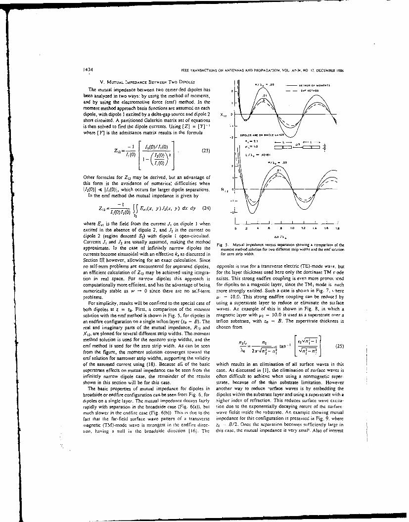
1434 IEEE TRANSACTIONS ON ANTENNAS AND PROPAGATION. VOL. AP-34. NO 12. DECEMBER 1986
V. MUTUAL IMPEDANCE BETWEEN Two DIPOLES -/A. - .05 -- 1-. 01 NONES. The mutual impedance between two center-fed dipoles has a -- ,, O
been analyzed in two ways: by using the method of moments,and by using the electromotive force (emf) method. In the I N
moment method approach basis functions are assumed on eachdipole, with dipole I excited by a delta-gap source and dipole 2 x, 0short circuited. A partitioned Galerkin matrix set of equationsis then solved to find the dipole currents. Using [Z] [Y1-' -'where [Y] is the admittance matrix results in the formula OoES AR O S, & LA, \ -
OAS AN NSNL L
A 50-l 12(o)/I,(0) (23) -
[ 2(0) ]-Other formulas for Z12 may be derived, but an advantage ofthis form is the avoidance of numerical difficulties when112(0)1 4 1i1(0)1, which occurs for larger dipole separations. 4, a
In the emf method the mutual impedance is given by-l II-
Z2 I ExI(x, y)J2 (x, y) dx dy (24)It(0)!a(0) 1J -2
S2
where EI, is the field from the current J, on dipole I whenexcited in the absence of dipole 2, and .J2 is the current on 0 2 .4 .6 .8 1.0 12 1.4 1.6 .a
dipole 2 (region denoted S2) with dipole I open-circuited. &XIx.Currents JI and J, are usually assumed, making the methodcurrentsJn 2ae iney n the Fig. 5. Mutual impedance versus separation showing a comparison of theapproximate. In the case of infinitely narrow dipoles the moment method solution for two different strip widths and the emf solution
currents become sinusoidal with an effective k, as discussed in for zero strip width.Section III however, allowing for an exact calculation. Sinceno self-term problems are encountered for separated dipoles, opposite is true for a transverse electric (TE)-mode wave, butan efficient calculation of Z12 may be achieved using integra- for the layer thickness used here only the dominant TM n odetion in real space. For narrow dipoles this approach is exists. This strong endfire coupling is even more pronou icedcomputationally more efficient, and has the advantage of being for dipoles on a magnetic layer, since the TM, mode is nuchnumerically stable as w - 0 since there are no self-term more strongly excited. Such a case is shown in Fig. 7, %.hereproblems. pI = 10.0. This strong endfire coupling can be reduce J by
For simplicity, results will be confined to the special case of using a superstrate layer to reduce or eliminate the surfaceboth dipoles at z = zo. First, a comparison of the moment waves. An example of this is shown in Fig. 8, in which asolution with the emf method is shown in Fig. 5, for dipoles in magnetic layer with 1A = 10.0 is used as a superstrate over aan endfire configuration on a single teflon layer (zo = B). The teflon substrate, with zo = B. The superstrate thickness isreal and imaginary parts of the mutual impedance, R12 and chosen fromX12, are plotted for several different strip widths. The momentmethod solution is used for the nonzero strip widths, and the nit, n2emf method is used for the zero strip width. As can be seen tan-
I _ _ 1 (25)
from the figure, the moment solution converges toward the Xo 2 r In , n [ f~n2,emf solution for narrower strip widths, supporting the validityof the assumed current using (18). Because all of the basic which results in an elimination of all surface waves in thissuperstrate effects on mutual impedance can be seen from the case. As discussed in [1], the elimination of surface waves isinfinitely narrow dipole case, the remainder of the results often difficult to achieve when using a nonmagnetic super-shown in this section will be for this case. strate, because of the thin substrate limitation. However
The basic properties of mutual impedance for dipoles in another way to reduce -urface waves is by embedding thebroadside or endfire configuration can be seen from Fig. 6, for dipoles within the substrate layer and using a superstrate with adipoles on a single layer. The mutual impedance decays fairly higher index of refraction. This reduces surface wave excita-rapidly with separation in the broadside case (Fig. 6(a)), but tion due to the exponentially decaying nature of the surface-much slower in the endfirc case (Fig. 6(b)). This is due to the wave fields inside the substrate. An example showing mutualfact that the far-field surface wave pattern of a transverse impedance for this configuration is presented in Fig. 9, wheremagnetic (TM)-mode wave is strongest in the endfirc direc- zo = B/2. Once the separation becomes sufficiently large intion, having s null in the broadside direction [16]. The this case, the mutual impedance is very small. Also of interest

JACKSON AND ALExI5POULos PLANAR STRIP GEOXIETRICS 1435
OIPOU.ES AR ONd SINGLE LAYER
f, . 10.0 x"ki- 1.0 100
16n,B - 10
LIS -n
1. -I I
10.
0 1. 2. 7 .
11 1.0 X.= 0.
n10 10..10
1.0 . 2.6 . 1 .0 1
=A is0 1.
LI.).,.-. 31.0 1.2 1. 5,
R'/ DIOE 0R LN / LE LAYER
101.0
1.5
00
00 ... .4L6 ..8.1.0.1.2 ...4 i's.I I
Ao /xo 0 2 .4 a .9 1.0 12 1A IS .s
(b)
Fig. 6. (a) Mutual impedance versus separation for dipoles in broadside A
configaration 0n00 single layer. (b) Mutual impedance versus Separation for Fig. 8. Mutual impedance versus separation for dipoles in endfire configura-dipoles in endfire configuration on a single layer. lion wih a superstrate used to eliminate surface weaves.

1436 IEEE TRANSACTIONS ON ANTENNAS AND PROPAGATION, VOL AP-34. NO 12, DECEMBER 1986
100 e. 2.1 -, = 12.5 Z
P, 1.0 2 0
nB_-6- 0 n2 I
-.2 L
Xl L L Z dZL
50 (a)
0
X =-
L/., = .34503
z.= B/2
(b)
-2 I I I I I I I I I
0 .2 .4 .6 .8 1.0 2 1.4 1A 1. x
A~x/xo
Fig. 9. Mutual impedance ersus separation for dipoles in endf'ee configura- TOP VIEW
lion embedded in the middle of the substrate. Fig. 10. Geometry of coupling betwech dipole and transmission line. (a)Dipole on top of superstrate. (bl Dipole at the interface.
is the almost monotonic nature of the curves in this case,which can be explained by assuming the superstrate acts as a bandwidth, Zd should not be too small. However, decreasingconductor for the space-wave fields, and using image theory. ZL lowers the coupling for a fixed Zd, so it is important toThe images will add in phase for zo and B - zo an odd number investigate ways of increasing the coupling. One approach isof electrical quarter-wavelengths in the substrate, to stack multiple dipoles above the line [18]. Another approach
is to choose a different material between the line and dipole.VI. DIPOLE EXCITATION By TRANSMISSION-LINE COUPLING Qualitatively, the coupling between the line and dipole may be
Another configuration which has been analyzed using the regarded as largely capacitive, which suggests an improvedmoment approach is the strip dipole excited by electromag- coupling using E2 > ti in the geometry of Fig. 10(a). To verifynetic coupling to a microstrip transmission line, shown in Fig. this, the end admittance is plotted versus offset for different10. This problem has been successfully analyzed with the dipole lengths in Figure Il(a) for the case of El = (2 = 2.1.moment method in the past for the line and dipole within a As can be seen, the coupling is not sufficient to allow for ansingle layer [17]. A 6-gap source is placed near the end of the input match with the layer thicknesses used. In Fig. 1 (b) theline as shown, and the same procedure as for the mutual same layer electrical thicknesses are used, but with C2 = 10.0.impedance is used to find the line and dipole currents. From In this case the couplirg is sufficiently strong to allow for anthis information the normalized admittance Y/Yo may be input match, for L/Xo = 0.186 and Lx/Xo = 0.123. In Fig.found, referred to the dipole-end of the line. For fixed line and 11(c) a magnetic superstrate is used, with /a2 = 10.0. Thedipole heights ZL and zd, an input match may be achieved by coupling in this case is not significantly different than the casevarying the dipole length L and offset in either the x or y of Fig. 11(a), supporting the conclusion of a capacitive-likedirections, provided ZL and Zd are sufficiently close. An offset coupling mechanism. A similar improvement in coupling isvariation in the x direction was chosen here in order to take possible when using stacked dipoles. The stacked dipoleadvantage of an efficient matrix storage procedure for the approach allows fo an even greater improvement in band-reaction values. The offset is then taken in integral number of width, but the total physical layer thickness will be largersubsections, Ax = N.d. when using E2 = f.
One of the main objectives in feeding a dipole in this manner The dipole can also be placed at the interface and excited byis to minimize the radiation from the line while maintaining a a line in the substrate, as shown in Fig. 10(b). In this case thesignificant radiation from the dipole. This implies keeping ZL superstrate is not improving coupling, but may be used tosmall, while simultaneously keeping a prescribed level of increase the efficiency of the dipole or achieve other desiredcoupling between the two. Also, to have a significant effects [I].

11JACKSON AND ALEXOPOULOS: PANAR STRtP GOMITRIS !437
2 == 22 = 2.2r
= 22 2to = 0.
= /.0 = ' ~ ,0,, w /* . 2 .o
n, I
04 r, s .00__
d/k oio4231
.. 0.JIIVE /k = .0,4473'
L~tI 9
3773
(a) (b)= 2.1 22 - 1.0
• o = 1.0 2 100
nB n.t
, = .o05
-!X, = .017307
L/),.- .3800
.4154
RI2 .2 5 0 20
(c)
Fig. 11. (a) Normalized end admittance versus offset for different dipole lengths with c2 =i 2.1. The offset along each curve isspecified by Ax = N-d with N = 4, 8, 12, 16, 20 corresponding to points 0, 0, 6, X, V, rspectively. (b) Normalized endadmittance versus offset for different dipole lengths with et = 10.0, e, = 2.1. The dashed curve shows a dipole length which allowsfor an input match. The offset along each.curve is specified by Ax = N-d with N = 3. 5, 7. 10, 11, 12 corresponding to points 0,0, 6, X, 9, + , respectively. (c) Normalized end admittance versus offset for different dipole lengths with 5,
= 10.0, f, = 2.1.
The offset along each curve is specified by Ax = N'd with N = 8, 12, 14, 16, 18, 20 corresponding to points 0, [, 4, X. 17. +,respectively.
1438 IEEE TRANSACTIONS ON ANTENNAS ANDS PROPAGATION. VOL. AP-34. NQ 12. LECEMBSES I9NB
VII. CONCLUSION for primntidcircutt antennas.' IEEE Trants. Antennas Propagor ,Vol.AP-33. pp. 976-987, Sept. 1985.
Four geometries consisting of planar strips in a substratc- 15, N. K. Uzunogau. N 0. Alenopoulos. and J. G Fiitors. 'Radiation
supcrstrstc configutrationl havc b~ccn atlalyzcd. intcludcing lte properrties of rticrostniptdipokcs.' IE Tro-r Antrens I'rolrugt.
microstrip transmission line, the Center-fed dipole, the Inutual vol. AP-27. pp. 853-858. Non, 1979. (Sec alSo colletion. IEEEimpeanc beweentwodiplesandthetranmis I . Trans. A4ntennas Propagat.. Vol. AP-3O. p. 526, May 1982.)
impdane etwen wodiple, ad te ranmision-line 161 0. M. Pozar. ''Imnpuo impedance and mutual coupling of rectangularcoupled dipole. The starting point in the analysis of each of microstrtp antennas," IEEE Trans- Antennas Propogot.. vol. AP-30.these was the plane-wave spectrum formulation for the pp 1191-1196 Nov. 1982.
171 L. E. Rana and N. Gl. Alexopoulos. ''Current distribution and inputreaction between two current sources. A real-space evaluation impedance of printed dipoles." IEEE Trans. Antennas Propagat.,technique for finding the electric field was also used, which vol. AP-29. pp. 99-106, Jan. 1981.improved the efficiency of the moment-method calculation for 181 E. J1. fDenlinger. "A frequency dependent solution for microsarip
transmission lines." IEEE Trans. Microwave Theory Tech., vol.mutual impedance, and also allowed for an easy determination M'Tr-l9. pp. 30-39. Jan. 1971.of the mutual impedance between infinitely narrow dipoles. 19) D. R. Jackson and N. 0. Alexopoulos. "An asymptotic extraction
For he icrstri trnsmssin lie, he moun ofdiser- technique for evaluating Sommerfeld-type integrals." IEEE Trans.For he icrstri trnsmssin lie, he moun ofdiser- A ntennas Propagat., pp. 1467-1470, this issuc.
sion was seen to significantly increase as a superstrate is added 1101 D0. M. Pozar. "Improved computational efficiency for the mtomentwhen e2 is much larger than 6 . The dispersion decreases as the method solution of printed dipoles and patches,.' Electroinagn , %ol. 3.line width decreases, although 13 must always be above the no. 3-4, ppt. 299-309, July-Dec. 1983.
1111 R. W. Jackson and 0. M. Pozar, "Fall-wave analysis of microstriplargest surface-wave pole. In the case of the center-fed dipole, open-end and gap discontinuities," IEEE Trans- Microwave Theorythe resonant length and input resistance were found from the Tech., vol. MTT-33. pp. 1036-1042, Oct. 1985.moment method and compared with simple approximate 1121 J. R. Wait. "Theory of wane propagation along a tin wre parallel to
an interface," Radio Sci.. vol. 7. pp. 675-679, June 1972.formulas. These approximate formulas allow for an easy 1131 R. A. Psacel and D. J. Masse, "Microstrip propagation on magneticextension of Hertzian dipole results to the resonant strip substrales-Part 1: design theory." IEEE Trans. Microwave Theorydipole. The mutual impedance between dipoles was then Tech., vol. MT't-20, pp. 3D4-308, May 1972.
1141 V. H. Ramsey. "Reaction concept in electromagnetic theory." Pity.investigated using both the moment method and the emf Rev., vol. 94. pp. 1483-1491. June 1954.method. The em! method allows for an efficient computation 1151 0. R Jackson and N. G. Alenopoulos, "Microstrip dipoles onfor the case of very narrow dipoles, and gives accurate rcsults electrically thick substrates," Int. 1. Infrared and Mitllnteter Naves.
whentheproer alu of ~ i usd i th assmedcurent 11 Jan. 1986.whe th prpervale o kis sedin he ssued urrnt.It1161 N. G. Aleuopoulos and 1. E. Rana, "Mutual impedance compttalon
was demonstrated that a superstrate may be used to signift- between printed dipoles." IEEE Trans. Antennas Propagat.. vol.cantly decrease the mutual impedance between dipoles, AP-29. pp. 106-11l. Jan. 1981.
[17) P. B. Katehi and N. 0. Alexdpoulos, ''On the modeling of electrotug-especially for dipoles in an endfire configuration, by reducing netically coupled tnicrostrip antennas-The printed strip dipole.,' IEEEor eliminating surface waves. Finally, results were Shown for Trans. Antenras Propagat., vol. AP-32, pp. 1179-1186. Nov. 1984.the case of a dipole excited by coupling to a transmission line, 1181 - "A bandwidth enhancement method for microstrip antennas.'" in
1985 IEEE Anrtennas Propaga. Soc. Symp. Dig., vol. 1, pp 405 -and it was verified that the coupling mechanism is predomi- 408.nantly capacitive. Hence the coupling is improved by using a 119) A. J. M. Snares, S. B. A. Fonseca. and A. J. Otarola, "The effect oframaterial with a higher dielectric constant between the line and dielectric cover layer on the current distribution and input impedanoce of
printed dipoles." IEEE Trans. Antennas Propagart.. Vol. AP-32. pp.dipole. 1149-1153. Nov. 1984.
REFERsENCES[1l N. G. Alenopoulos and 0. R. Jackson, ''Fundamental superstrule
(cover) effects on printed circuit antennas," IEEE Trans. Antennas David R. Jackson (S'83-M'84), for a photograph and biography please sePropgat.. vol. AP-3), pp. 807-816, 1984. page 816 of the August 1984 issue of this TRANSACTIONS.
[21 - ''Fundamental saperstrate (cover) effects on printed circuitantennas," UCLA Rep. ENG-83-50. Oct. 1983.
Il1 N4. G. Alenoporslos. D. R. Jackson. and P. B. Katehi, "Critria fornearly ormidirectional radiation patterns for printed antennas," IEEE Nicdnaon G. Atenopoulos (S'68-M'69-SM'82). for a photograph andTrans. Antennas Propagat., vol. AP-33. pp. 195-205, Feb. 1985. biography please see page 39 of the January 1983 issue of this TRANSAC-
14) D. R. Jackson and N. G. Alexopoulos. "Clain enhancement methods TIONS,
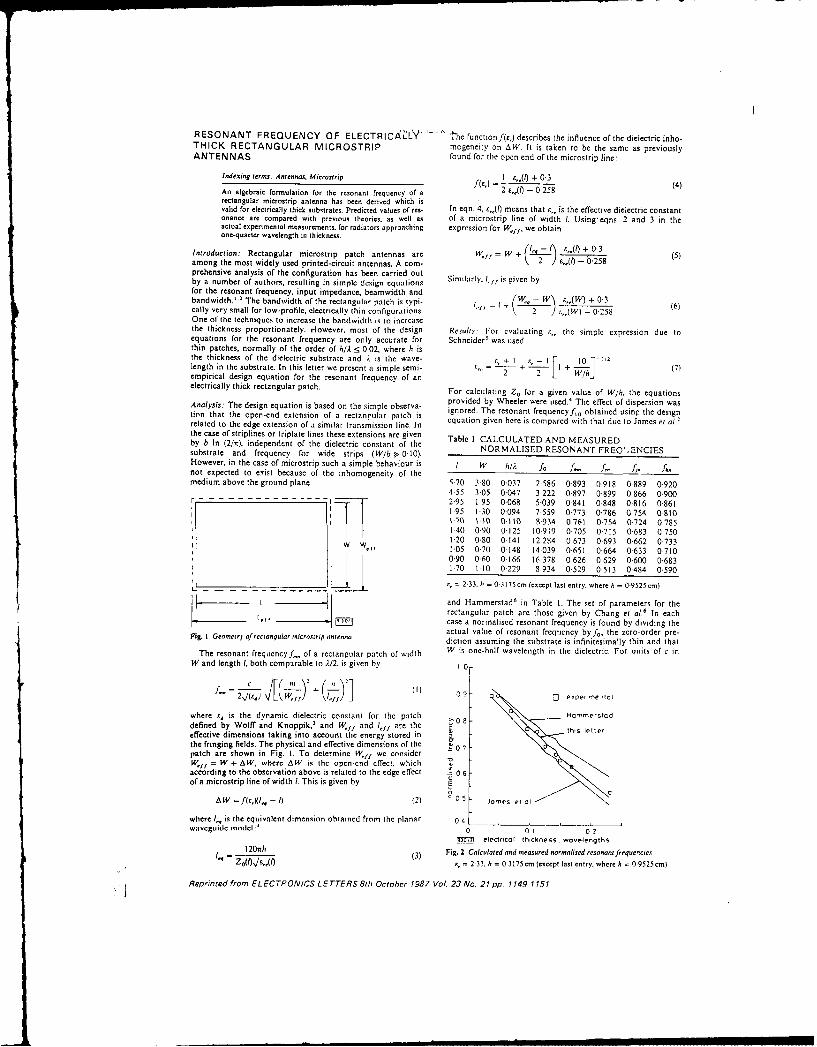
RESONANT FREQUENCY OF ELECTRICAL1Y 'the functtonf(,) describes the influence of the dielectric inho-THICK RECTANGULAR MICROSTRIP mogeneity on AW. It is taken to be the same as previouslyANTENNAS found for the open end of the microstrip line:
Indexing terms Antennas, Microstrip I s,e() + 0.3
An algebraic formulation for the resonant frequency of a 2 c,(O) - 0'258rectangular microstrip antenna has been derived which isvalid for electrically thick substrates. Predicted values of res. In eqn. 4, r,,() means that ,, is the effective dielectric constantonance are compared with previous theories, as well as of a microstrip line of width 1. Using eqns. 2 and 3 in theactual experimental measurements, for radiators approaching expression for WV,,., we obtainone-quarter wavelength in thickness.
Introduction: Rectangular microstrip patch antennas are WfJf = w+ 12 c_(I) + 0 3 (5)among the most widely used printed-circuit antennas. A corn- 2 ) T - b 2558prehensive analysis of the configuration has been carried Outby a number or authors, resulting in simple design equations Similarly. 1., is given byfor the resonant frequency, input impedance, beamwidth andbandwidth.
" The bandwidth or the rectangular patch is typi- (W, - W c F(4 + 0'3
cally very small for low-proile, electrically thin configurations. . = ' \ 2 / i.,_(W - 0258 16)One of the techniques to increase the bandwidth is to increasethe thickness proportionately. However, most of the design Results: For evaluating :,, the simple expression due toequations for the resonant frequency are only accurate for Schneider was used:thin patches, normally or the order of h/A < 0.02, where It isthe thickness of the dielectric substrate and . is the wave- r, + I 1, - t [ 10"length in the substrate. In this letter we present a simple semi- .. = + Iempirical design equation for the resonant frequency of anelectrically thick rectangular patch. For calculating Za for a given value of W/h, the equations
Analyaia: The design equation is based on the simple observa- provided by Wheeler were used.' The effect of dispersion wastion that the open-end extension of a rectangtular patch is ignored. The resonant rrequencyfno obtained usinr the designrelated to the edge extension o r a similar transmission line ti equation given here is compared with that due to James el a/.'the case or striplines or triplate lines these extensions are given Table I CALCULATED AND MEASUREDby b In (2/n), independent of the dielectric constant of thesubstrate and frequency for wide strips (W/b > 0"10). NORMALISED RESONANT FREO'ENCIESHowever, in the case of microstrip such a simple behaviour is I W h/. fA .-, fr fi, fA.not expected to exist because of the inhomogeneity of themedium above the ground plane. 5'70 3-80 0"037 2.586 0893 0918 0'889 0"920
4.55 3-05 0047 3-222 0.897 0899 0866 0.900-- 2"95 1.95 0"068 5039 0841 0848 0816 0.8611,95 130 0094 7-559 0773 0.786 0754 0,81010 110 OWttO 8934 0761 0.754 0724 07851.40 0"90 0.125 101919 0.705 0.715 0.683 0750120 0.80 0141 12284 0673 0693 0662 0733w W , 1-05 070 0-148 14039 0651 0664 0633 07100'90 0"60 0"166 16.378 0626 0629 0"600 0683
1,70 I 10 0229 8.934 0.529 0513 0484 0.590r':, = 2.33, h = 03 175cm (except last entry, where h = 09525 cm)
and Hammerstad' in Table I. The set of parameters for therectangular patch are those given by Chang et al.' In eachcase a normalised resonant frequency is found by dividing theactual value of resonant frequency byfo, the zero-order pre-
Fig. I Geometry ofrecsangulor microstrip anteeno, diction assuming the substrate is infinitesimally thin and thatThe resonant frequencyf,, of a rectangular patch of width W is one-half wavelength in the dielectric. For units of c in
W and length 1, both comparable to A/2, is given by 1 0
2r(,) (-W, )I + I 9 0 exoere-tal
where E, is the dynamic dielectric constant for thle patch " Horrnerstcddefined by Wolff and Knoppik,. and Wff and l, urn the teffective dimensions taking into account the energy stored in a
the fringing fields. The physical and effective dimensions ofr thepatch are shown in Fig. I. To determine Wff we consider 07
W.'t = W + AW, where AW is the open-end effect, whichaccording to the observation above is related to the edge effect . 0 6or a microstrip line of width I. This is given by E
A W =f(r,Xl,• - 1) (2) 0 5 Jonres et al
where I,, is the equivalent dimension obtained from the planar 0 cwavguidc 15...dei :" 0 0 1 2
L t33l eleclreoil thwekness, wavelengths1207nh (3) Fig. 2 Calculated and measured normalised resonant frequencies
, Zo 'A"( 111 ,(() r., = 2-33, h = 03175cm (except last entry, where h = 09525 em)
Reprinted from ELECTRONICS LETTERS 8th October 1987 Vol. 23 No. 21 pp. 1149-1151

u nctc /IcoII I and o ' CCCor4 CH - tic- , - (' eeaccl5/(W/tj,)GHz. The entries forJ.f,.,f, and f, thus rep-resent, respectively, the values measured, calculated by thismsethsod, calculated by James et al., and calculatCd by -ant- I BAHL, t. .and attARtA. "Microssip antennas' (Artech House,merstad divided by the appropriate fa. The graphical repre- 1980)sentation of these data in Fig. 2 shows that the resonantfrequencies predicted here lie in between those c~alculated by 2 tAMFS, ]. R,.. tALL, p. s., and WooD. c. 'Microstrip antennas-the other two methods, and are closer to measured values for theory and design' (Peter Peregrinus, 1981)most of the cases. An overall accuracy of approximately 3%was found for values of electrical thickness li/r < 0 229. 3 votlv, I.. and r NorP. N.: 'Rectangular and circular inscrostrp
disk capacitors rvd resonators'. IEEE Trans., 1974, MTT-22, pp.Acknowh'lments: This work was supported by the US Army 957-864Resetrch Offlice through contract I)AAG29-84-K-I0166 iCdl by
Texas Advanced Technology Research Pro- 4 rUIA. K. C:.. GAr, K., and uAHL, C. ;.: "Mtcrostrp lines inCtd slut-a grant from the lines'(Artech House, 1979)gramme.
5 SCHNIFIDER, m. v. 'Microstrip lines for microwave integrated cir-R. GARG 18th Aucust 1987 cuits'. Bell S9,st. Tech. J., 1969, 48, pp. 1422-1444S. A. LONG
Department of Electrical Enrrneering 6 CHIANG, L.. LONG. S, A., and RICHAROS, w. r.: 'An experimental
University of Houston investigation of electrically thick rectangular microstrp antennas'
Houston, TX 77004, USA IEEE Trus.. 1986, AP-34, pp. 767-772

APPENDIX H
570 IEEE TRANSACTIONS ON ANTENNAS AND PROPAGATION, VOL 36, NO. 4, APRIL 1988
Communications
An Improved Formula for the Resonant Frequencies of RESONANT FREQUENCIES OF AN EQUILATERAL TRIANGULAR PATCH
the Triangular Microstrip Patch Antenna ANTENNA (a = 10 cm a, 1 2.32, AND h = 0.159 cm)
RAMESH GARG AND STUART A. LONG. SENIOR MEMBER, IEEE Measured Calculated (GHz)Mode GHz a,,, and e,, I1] a, and f, Ill a, and ,,
Abstract-An improved formula is derived to predict the resonant TM. 1.280 1.413 1.299 L273frequency of the triangular microstrip patch antenna. The technique TM,... 2.242 2.447 2.252 2.239previously used for the case of a circular disk is modified to produce TM,... 2.242 2.426 259 2.546
prouce TM~., 2.550 2.826 2,599 254greater accuracy than previous investigations. TM2.1.-, 3.400 3.738 3.439 3-419
INTRODUCTION TM, 0., 3.824 4.238 3.899 3.819
Recently, Dahele and Lee [I have reported on the resonantfrequencies of an equilateral triangular microstrip patch. The REFERENCES
calculated values of these frequencies, based on an effective length 11) J. S. Dahele and K. F. Lee. "On the resonant frequencies of the
an and an effective relative pernittivity cs,, have been compared with triangular patch antenna,- IEEE Trans. Antennas Propagat., vol.
measured values. A comparison with measured values, however, AP-35, pp. 100-101, Jan. 1987.[2] L. C. Shen and S. A. Long, "The resonant frequency of a circular disc,
shows some reasonable difference between the two. Here, we show printed-circuit antenna," IEEE Trans. A ntennas Propagot., vol. AP-
that if a different effective length and just the actual substrate 25. pp. 595-596, July 1977.permittivity arc used, the computed values arc mtch closer t the (31 Y. Suzuki and T. Chiba. 'Computer analysis method for arbitrarilymeasured values, shaped microstrip antenna with multiterminals." IEEE Trans. Anten-
nas Propagat., vol. AP-32, pp. 585-590, June 1984.
CALCULATIONS
To compute the resonant frequency of an equilaleral triangularpatch, the effect of the fringing field can be assumed the same ias that
of an equivalent circular disk which has the same metalized area as
the given triangular patch. Previously, the effective radius a, of the
circular disk was given [21:
2h nra+ 2O,=Oa ++ 1n± . 7 7 26) (1)
where a is the radius of the disk and h is the substrate thickness. Thtsformula can then be modified to provide a reasonably accurateprediction of the resonant frequency of the triangular patch by
substituting an equivalent sidelength, a,, into (1) in the place of a tothen produce a new effective sidelength. This can be done by defininga. such that S = waq where S is the area of the original triangularpatch. Then this value of a, can be used in the formula for the
resonant frequency [1]:
2c.,)' (/it" +Int + it)-
()
where c is the velocity of light and the integers ii. n, I satisfy the
condition Mn + n + / = 0.This approach was first suggested by Suzuki and Chiba [3] for the
case of a pentagonal patch. The results are shown in Table I, alongwith the previous theories [1] and experimental data. As can be seen
the new method consistently predicts resonant frequencies moreaccurately through the first five resonances.
Manuscript received August 20, 1987. This work was supported in part bythe U.S. Army Research Office under Contract 0AAG29-84-K-0166 and by agrant frost the Texas Advanced Technology Research Program
The authors are with the Department of Electrical Engineering. Universityof Houston, Houston, TX 77004.
IEEE Log Number 8719160.
0018-926X/88/0400-0570$01.00 ©} 1988 IEEE

APPENDIX IIEEE TRANSACTIONS ON ANTENNAS AND PROPAGATION. VOL. 36. NO 7. JULY 1988 905
A Leaky-Wave Analysis of the High-Gain PrintedAntenna Configuration
DAVID R. JACKSON, MEMBER, IEEE, AND ARTHUR A. OLINER, LIFE FELLOW, t-EEL
Abstract-A leaky-wave analysis is used to explain the narrow-beam Substrate - Suoerstrate Geometry"resonance gain" phenomenon, in which narrow beams may be producedfrom a printed antenna element in a subslrate-superstrate geometry. The Ileaky-wave approach furnishes insight into the physical processes in-volyed, provides new practical information, and permits the derivation ofsimple asymptotic formulas for the leaky-wave properties and for the zradiation behavior. Results are presented as a function of frequency, thescan angle, and the e of the superstrale.
I. INTRODUCTION
1V
R ECENTLY, a method for increasing the gain of aprinted-circuit antenna involving the use of a superstrate
layer was discussed [1]. In this method the antenna element is Fig. I. Two-layered geometry with embedded dipole antenna element fromwhich narrow beam can be radiated. E2 (or p2) of supersrate (upper layer)embedded within a two-layered geometry consisting of a must be greater than e, (or jit) of substrate. Horizontal antenna element is
bottom (substrate) layer of thickness b having relative permit- located at height z, and peak of radiated beam occurs at angle 0,.tivity and permeability e1, g,, and a top (superstrate) layerhaving parameters E2, I.2, as shown in Fig. 1. As explained in resultant decrease in beamwidth. Asymptotic formulas for[1], a narrow beam about any desired angle Op may be obtained gain and beamwidth are presented in [1]. Although providingfor 62 > I or uz ;" I when the layer thicknesses are chosen for convenient formulas, this derivation does not by itselfproperly. In particular, the following dual types of "resonance provide any insight into the fundamental cause of the narrow-conditions" are discussed in [1]. bean phenomenon.
In this article it is shown that the resonance gain effect mayCase I.- be elegantly described in terms of leaky waves. It is
nib 7 demonstrated that the phenomenon is attributable to the1- sin' 6,1n! = 1- (1) presence of both transverse electric (TE)- and transverse
2 magnetic (TM)-mode leaky waves which are excited on the
n 2t structure. Asymptotic formulas for the leaky-wave properties1- sin 2 4 (2) are derived, which demonstrate that the attenuation rate of the
leaky waves decreases as the gain of the pattern increases. Theforoa E 1. migration with frequency of the leaky-wave poles in the
Case 2: steepest-descent plane is also discussed, and it is shown thatseveral important physical effects are confirmed by thatsin 2 0b / n- (2m - )investigation. Radiation patterns based on the relevant leaky,
2o 2
the dominant role of the leaky waves in determining theI -sin 2 0
./n= (2p - l ) (4) pattern. One practical result of this investigaion is a simple
X0 4 rule for determining the size of the structure necessary to
for ,s2 1, where n, = T n2 = -,/t72 and in, n are produce the narrow-beam patterns, a result which would bepositive integers. difficult to obtain otherwise.
When (1), (2) or (3), (4) are satisfied, the gain at 0O becomes Due to the similarity of results, only case 1 (E 2 )> 1) will be
increasingly large as E2 --, or ,A2 -- o, respectively, with a discussed. This is the more practical of the two cases, sincelow-loss high-permeability materials are difficult to obtain.
Manuscript received March 20, 1987; revised September 24, 1987. This II. LEAKY-WAVE POLES AND THE STEEPEST-DESCENTwork was supported in part by the Army Research Office under Contract REPRESENTATIONDAAG29-84-K-0166.
D. R. Jackson is with the Cullen College of Engineering, Lniversity of The theory of leaky waves and their role in determining theHouston, 4800 Calhoun Road, Houston. TX 77004. radiation behavior of certain antennas is well established [2]-
A. A. Oliner is with the Polytechnic University, 333 Jay Street, Brooklyn, [7]. To emphasize the main points, the analysis for the case ofNY 11201.
IEEE Log Number 8820226. a horizontal Hertzian electric dipole in the stratified medium
0018-926X/88/0700-0905501.00 © 1988 IEEE

906 IEEE "IRANSAC I (NS ON AN I LNNAS AND IPROP'AGA IION, VOL 36. NO 7. JULSY 19
k,- pne , functions 19] i(i tintc giation vitablc k,. /2, and D, havczcros on tie real axis of the k, plane in the range k0 < k, :max (k,), whcre k, is the wavcnumber in (he ith layer. Thesezeros correspond to TE- and TM-node surface waves,
Q!7, k,, respectively. The integration path goes around these poles, as-ke ko shown in Fig. 2(a). Branch cuts from the branch points at ± ko
£ are also necessary to define the proper branch interpretation ofk., which is Im (k,) < 0, corresponding to fields that decay asz increases.
(a) The steepest-descent transformation
plane W k, = k0 sin - (9)
k. =ko cos " (10)
then results in an integration along the contour F in the
-7r/27 LW 2 steepest-descent -plane, shown in Fig. 2(b). This contourmay be deformed into the steepest-descent path (SDP) whichpasses through the saddle point at 0 = , where R, 0,describe the observation point in spherical coordinates with r
r" = R sin 0, z - h = R cos 6. The far-field evaluations of (7),(8) may be obtained via the saddle point method in the usualway [7]. It is important to recognize that the single-sheeted
(b) steepest-descent plane as a whole is neither proper nor
Fig. 2. (a) k-plane, where k, is wanenumber transverse to z direction, improper, but in fact portions of it are proper and otherSurface-wave poles lie along real axis (denoted by x's) and branch cuts portions improper. The semi-infinite strip for which 0 < , <(wiggly lines) emanate from branch points ±k,. Integration path r is r/ 2 and , < 0 is an improper region (Im (kz) > 0). Complexdeformed around surface-wave poles in accordance with conventionalassumption of infinitesimalloss (and e" time dependence). Branch cus are zeros of D,(k,), D,(k,) may exist in this region at .. + J u,chosen so that upper Riemann sheet is proper, whereas lower Rieman:i which result in TE- and TM-mode "leaky-wave" polessheet is improper. Leaky-wave poles occur on improper (lower) sheet. (b) (LWP). Complex poles can only occur in the improper regionSteepest-descent plane corresponding to rime dependence e'". Saddle-pointis present at f = 0 on real axis, and example is given of leaky-wave pole for the lossless case when ci > 1, 1A, > 1 [2]. Hence the onlyand surface-wave pole captured by deformation front original path r to other poles in the [-plane are the surface wave poles (SWP),steepest-descent path. which lie along the lines P, = - 7/2, as shown.
If 0 is sufficiently large, some leaky-wave poles will in
of Fig. 1 will be considered. Starting with the classical general be captured during the path deformation, as shown in
Sommerfeld solution [8], the expressions for the fields are Fig. 2(b). The leaky-ave fields increase exponentially with
written in terms of the Hertzian magnetic vector potential I1 as z, but decrease exponentially with R within the region inwhich they are defined, since 0 > [', when they are captured
fi=jiV x II (5) [2]. The leaky-wave phase and attenuation constants are givenby
E'=k~fl,+ V(V. f"). (6) .b =Re (k,,)=Re (k0 sin (p)= ko sin (,. cosh 'ip (11)After solving the boundary-value problem for fl, the two
components of the potential FI, and I, may be written in the n = - Im (k,p) = - Im (k5 sin f'p) = - ko cos ',, sinh (,,,
region z > h as (suppressing e J'') (12)
S+ -Ukr) respectively, where 3 - ja is the pole location in the k,-plane
fI,(r, z) e-Jkt(: -h)H(2) kr) dk, (7) (on the improper sheet5. If a leaky-wave pole is close to the
D(k,) "real axis so that cc is sufficiently small, the leaky-wave field
will dominate the total field at the air-dielectric interface,
Ila(r, z)=cos 4i g(k) eiAZI:-') H(l(krr) dk, provided the residue is not too small [3]. In this case the-- D,(k,)D,(k,) radiation pattern exhibits a sharply peaked behavior at 0 = Op
() where8 e= ko sin 0p. (13)
where A more detailed discussion of leaky-wave properties is given
in [2], [3].
Ill. ASYMPTOTIC EVALUATION OF THlE LEAKY-WAVE PROPERTIES
k,= -k "I/- ) .In view of the previous discussion, it may be expected that
In these expressions f, g, D,, and D,, are complicated leaky waves could be responsible for the high-gain effect. This

JACKSON AND OUNER: IIGH-OGAIN PRINTED ANTENNA CONFIGURATION 907
presumption may be verified by a straightforward, but wherelengthy, asymptotic solution for the leaky-wave pole locationsof the characteristic equations, which are as follows. a - (n5 - sin2
8 )312 cot 0O (19a)m-r JAI
TE-Mode:D,= O =cos (k2 1)[nhU (jkob) + (k, Ib) cot (k,,b)j - C ,I2 - sin 2 0V) '/ (sin 0,, cos 0,) -(19b)
1717r
sin (k,21) JAI.k It -(k: 2 )(k 2 b)
-j112(kIb)(kst) cot ( .1b (14) r
I 2Several important conclusions follow from these results.
TM-Mode: First, there exists a TE-mode and a TM-mode !eaky-wave polewhich both become dominant (a - 0) for c2 > 1. For these
D,,,=0=cos (k.2t)[j(kob)ej-(k 1 b) tan (klb)] dominant poles 0/ko - sin 0. when 6 > 0, in agreement withsin (k,20 the conclusion of a peaked beam at O, due to the leaky waves.s~ k - (k 2t)(kz2b) For Op > 0 the attenuation constant a behaves as Q(0/E2). For
k L2t the case 0, = 0, 3/ko tends to zero, but relatively slowly,
+jE((kbb)(k)ot) tan 'kib1 (15) behaving as O(1/-,/'2). In this case, cko has the same
I asymptotic form as O/ko, and hence the leaky-wave pole
where asymptotically approaches the origin along the diagonal line,2 - 2 /2 in either the k,-plane or the i-plane. Furthermore, in this case
k0 o- ,) the form is the same for both the TE- and TM-mode poles.kz = (k2-k2)1/2 To verify the validity of the asymptotic formulas, results
showing a comparison of the exact and asymptotic leaky-wave2 (k I- k,, /2. propagation wavenumbers for the TE-mode case are presented
The sign taken for the square root of k,,, k,2 is arbitrary since in Fig. 3 for a broadside beam, and in Fig. 4 for a scannedthese signs occur in even function fashion in (14) and (15), but beam (0, = 45"), for the lowest mode (m = , p = 1). TheIm (ko) > 0 is used to ensure the improper pole interpreta- exact values are found by a secant-method search in thein 0 ucomplex plane. The agreement is good in all cases, andtion.
To solve for complex pole locations asymptotically, k, is improves as E, increases.written as a perturbation about the expected high-gain value as One of the practical uses of these formulas for the leaky-
wave properties is in determining the required structure size ink,=ko sin 8,+ko(6,+j~i). (16) the x, y directions to realize the narrow beam patterns. The
The arguments of the tan and cot functions may then be size required is such that the leaky waves emanating from theapproximated for the cases 0, > 0 and 0, = 0 and then dipole are sufficiently attenuated at the perimeter. If thesubstituted into (14), (15), with only the dominant terms kept structure radius is r,, then or, > I is required.as E2 - co. After straightforward but lengthy simplification,the results summarized below are obtained. IV. LEAKY-WAvE RADIATION PAd-rmiRNs
TE-Mode: The TE-mode leaky wave primarily determines the E,component of the far field, while the TM-mode waveprimarily determines E0. The TM-mode leaky wave thus
O/k0-sin 0, (17a) determines beamwidth in the E-plane, while the TE-mode/ko - a,/ 2.- (17b) wave determines beamwidth in the H-plane. Because the
asymptotic form for a/k1 is the same for the TE- and TM-0, = 0: modes when Op = 0, a broadside pencil beam is produced
which is circular in shape. For a scanned beam the forms are0/ko - a/ko -c, 2. (17c) different, so a conical beam having different beamwidths in
the two planes is created.TM-Mode: For the H-plane, it is possible to predict easily the leaky-
,, > 0: wave radiation pattern 'ising scalar diffraction theory. This is
/3/k0 - sin 0p (18a) because the H-plane pattern of the dipole is the same as thatfor an infinite line source in the x direction. Because of the
elko-b/C 2. (18b) two-dimensional nature of the line-source problem, a scalar
0= 0: Kirchhoff-Huygens formulation may be used to determine theradiation field from the amplitude distribution of the leaky-
O lko-otlko-cjl/l' (18c) wave on the layer surface. Derived in [3], the formula for the

AN I t..N AS AND PROPAGATION. VOL 30. NO
0.73 E,
0.5 - 1- - *.y000,,
k3 vs.O~6 6 s0.72 1., 0
0.4 0
- E ... 0.71
0.3 0.70
0 . I I I
0 10 20 30 40 50 60 70 8C
0.2
(a)
010 i/k. 0 2
0.1
- - AE,0Ict
6,02.l
0 1 2 0 30 40 50 60 70 80 90 01
0
E2 .0.05
(a) o
0.5
0 / 60 0s. %
0.4
\0 10 20 30 40 50 60 70 80M- - A .6,o'Ic
0.3 0o E20 (b)
S.0Fig. 4. Same as Fig. 3, but for 0, = 45 (scanned beam). Note th..1. 0 .4(a), for /ko, ordinate scale is greatly enlarged.
0.2
radiated power pattern is
cos 0 2.
0.1 -. RO"~~an t O
To provide a convincing demonstration of the don
nature of the leaky waves in determining the pattern, the
0 , , , H-plane radiation pattern (from a reciprocity method0 °o3 20 3 40 50 60 70 80 90 compared with (20) for the lowest mode (m = p = 1) ir
C2 5(a) and (b) for Op = 0' and Op = 45, respectively
(b) patterns are normalized to 1.0 at the maximum).Fig. 3. Comparisons between exact and asymptotic TE-mode leaky-wave agreement is excellent in both cases.
propagation wavenumbers as function of dielectric constant f, of super. Since the asymptotic formulas for c/ko do not depend ostrate, for lowest mode with 0, = 0. (broadside beam). (a) Phase constant dipole position zo but only on the layer parameters./3/k versus . (b) Attenuation constant or/k versus e. beamwidlth and gain of the pattern are likewise independe
zo in the asymptotic limit. The amount of radiated powc
however, dependent on the dipole position. The optit

A I-' U. 0
1O 1 Leaky - Wave Pole Locations vs f,
*IE- eo. I
-- .... 0.5 _
\\ -- W L 05,. TE S. -
, o2 T.,....o.5.o We .
00.55
l ~ /SDP (8" / 2 )
(
-10 X f .1 n b 0 -5f
0 5 10 15 20 25 30 3S 40 45C
2-O. 2s 1,
E( g.)
10LJv 1.0 .2o -O 25 1,
(a)
n-O1 va. 0
Fig. 6. Migration of leaky-wave poles in steepest-descent plane withnormalized frequency f,, for lowest mode with t2 = 10. Interval between
- Ea., t data points is 0.10.-- Leaky Wae
C,-,2.1 introducing a frequency ratio f, and then using layer,U, =,.0 thicknesses according tof, 0O.0
0- = 0. 5f, (22a)
/ = 0.25f, (22b)
/ with el = 2.1, 62 = 10, and i = I2 = I-
At low frequency the radiated beam has a maximum atbroadside with a relatively low gain. For low frequency boththe TE- and TM-mode poles lie significantly below the real
2 0 35 4'0 45 50 5s no axis, as seen in Fig. 6. As f, increases toward 1.0 the8 (deg. ) broadside beam narrows, with a maximum broadside gain
(.) obtained forf, = 1.0. At this point conditions (22a) and (22b)Ib) then correspond to the resonsance condition for 0a = 0 for the
Fig. 5. Comparisons of exact and leaky-wave H-plane radiation patterns for lowest mode (m = I, p = 1) as given by (1) and (2). In thelowest mode with e, = 10. (a) 0, = 0'. (b) e, = 45". Agreements are seento be excellent, steepest-descent plane both poles are seen to come near to the
origin at.f, = 1. At this point - r' = (,, in accordance withdipole height to maximize radiated power is the prediction, made in association with (17c) and (t8c), that
for large e2 the poles would lie near to the origin along the
- ,/ - sinO/,n =_(2n- 1), n=l, 2, .- (21) diagonal line.0 4 Asf, increases past 1.0 the beam scans, since (1) is thensatisfied for larger values of 6,; (2) will then not be satisfied
where zo < b. This places z0 at a voltage maximum position in exactly, but this feature is not too significant in determininga transmission-line model of the layered structure (I]. the resonance condition. It is primarily the substrate thickness
that determines the beam scan angle. The scanned beam isV. POLE MIGRATION WITH FREQUENCY conical in shape, having a narrower beamwidth in the H-plane
Some interesting features can be observed as the leaky-wave than in the E-plane. These results are in agreement with thepole positions are traced as a function of frequency in the pole behavior for f, > 1.0 in Fig. 6. As f, increases, (,steepest-descent plane. In Fig. 6, such a plot is obtained by increases for both poles. However, (4ij decreases steadily

IEEE TRANSA IIONS ON ANTENNAS AND PROPAGATION, VOL. 36. NO. 7. 1;
for the TE-mode pole but begins increasing for the TM-mode of the leaky waves tends to zero as e2 increases, beha'pole. The attenuation constant a is thus smaller for the TE- O(1/E 2) for a scanned beam (0, > 0), and as O(1/-mode pole, in accordance with (17b), (18b) which predict that broadside beam (0, = 0). The phase constant 0 of tn,the TE-mode pole is less attenuated when Ez 2 1. waves tends to ko sin 0p for 0 > 0 and tends I,
Also shown in Fig. 6 is a portion of the steepest descent path asymptotically in the same form as a when 6,(dashed line) for the case of a saddle point at " = 0 = wr/2, Asymptotic formulas for the explicit behavior havewith the path described by sin ?, cosh ('i = 1. All leaky-wave presented. One practical application of these formulapoles to the left of this line will be captured for some angle 0, simple rule for determining how large the structure ra,while those to the right are never captured. This path also needs to be to realize the narrow beam: or, ) I.serves as a dividing line between fast waves (0i < k0) to the The TE-mode leaky wave determines the H-plane p;left and slow waves (0 > k 0) to the right, seen from (11). while the TM-mode leaky wave determines the EHence all leaky-waves poles which are captured, and thus pattern. In the H-plane, the pattern due to the leaky w,directly contribute to the fields, are fast waves. From Fig. 6 it itself may be computed from Huygen's principle, at:is seen that both the TE-mode and TM-mode poles cross the results show excellent agreement with the total rad7r/2 steepest-descent curve, but at different frequencies. The pattern, furnishing additional proof that the fields at thepoles continue to proceed into the slow wave region, intersect- interface are indeed dominated by the leaky waves. The Iing the line ', = 7r/2. In the lossless case, poles in the i-plane wave approach discussed in this paper provides both siare symnetrically located about the line , = 7/2 [2]. Hence, cant insight into the physical processes involved in the naat the intersection frequencies the poles merge with their beam resonance gain phenomenon, and methods to deri\symmetrical counterparts, which are also improper poles. As relevant expressions in much simpler ways.f, increases further, the pole pairs split. For each pair, onepole proceeds downward along the line r = 7/2, and REFERENCES
represents an improper surface wave pole, which is never 1] D. R. Jackson and N. G. Alexopoulos, "Gain enhancement ni
captured for any angle 0. The other pole moves upward from for printed circui antennas," IEEE Trans. Antennas PropagotAP-33, pp. 976-987, Sept. 1985
the intersection point along the line 7r/2, starting as an [2) T. Tamir and A. A. Oliner, "Guided complex waves: Pan 1, F,improper surface-wave pole. This pole crosses the " = 7r/2 an interface," Proc. Inst. Elec. Eng., vol. 110, pp. 310-324
point (real axis) at the frequency corresponding to a TE or TM 1963.131 - , "Guided complex waves: Part 2, Relation to radiation pant
surface-wave cutoff frequency, for the respective pole type. Proc. Inst. Elec. Eng., vol. 110, pp. 325-334, Feb. 1963.The pole continues to move upward as f, increases, becoming 14 -, "The influence of complex waves on the radiation field of.
a proper surface-wave pole. The two upward-moving poles excited plasma laver," IRE Trans. Antennas Propagat., vol. App. 55-65, Jan. 1962.may then be identified as the usual TE2 and TM 2 surface-wave [5] S. Barone, "Leaky wave contributions to the field of a line s
poles, respectively (for the indexing used here, the TM0 and above a dielectric slab," Microwave Res. Inst., Pol)technic
TE, modes have the lowest cutoff frequencies of their Brooklyn, Rep. R-532-56, PIB-462, Nov. 1956.[6] S. Barone and A. Hessel, "Pan t--Leaky wave contributions
respective mode types, with the TM0 mode having zero cutoff field of a line source above a dielectric slab," Microwave Res.frequency). Polytechnic Inst. Brooklyn, R-698-58, P53-626, Dec. 1958.
Although only the TE2 and TM2 poles are shown in Fig. 6, 17] L. B. Felsen and N. Marcuvitz, Radiation and ScatterinWaves. Englewood Cliffs, NJ: Prentice-Hall, 1973.
there are an infinite number of both TE- and TM-mode leaky- [8] A. Sommerfeld, Partial Differential Equations. New York:wave poles [6], although only a finite number are captured by demic, 1962.the steepest-descent path (and hence contribute directly to the 191 N. G. Alexopoulos and D. R. Jackson, "Fundamental super
effects on printed circuit antennas," IEEE Trans. Antennas Pifield) at any given frequency. Only the TE2 and TM2 poles are gat., vol. AP-32. pp. 807-816, Aug. 1984.
dominant, however, with the others being further away fromthe real axis. All of the leaky waves exhibit a similar behaviorregarding the intersection with a symwctrica image pole on David R. Jackson (S'83-M'84) was born i
the 7r/2 line, however, with the upward-moving pole crossing .I Louis, MO, on March 28, 1957. He obtainec
the r/2 point at some frequency, corresponding to a surface- I B.S.E.E. and M.S.E.E. degrees from the Unisity of Missouri, Columbia, in 1979 and P
wave cutoff frequency. In this way all leaky-wave poles may respectively, and the Ph.D. degree in elect
be indexed according to their corresponding surface wave type engineering front the University of California.and number. Angeles, in 1985.
He is currently an Assistant Professor inVI. CONCLUSION Electrical Engineering Deparinent at the Univet
I of Houston, Houston, TX. His research interest
The narrow-beam resonance gain phenomenon discussed in present inclade mricrostrip antennas and pri
[1] is shown to be attributable to the excitation of weakly
attenuated leaky waves on the structure. Both a TE- and a TM-mode leaky wave become dominant for e2 a> 1, where Arthur A. Oliner (M'47-SM'52-F'6l-LF'87) for a photograph and binsubscript 2 refers to the superstrate. The attenuation constant cy phy please see page 1294 of the December 1985 issue of this TRANSACT(

I~~ ni to 25. mm. I I I
APPENDIX J to254mram.
Results: Typical impedance and insertion loss plots are shownin Fig. 2 and Fig. 3 for the case r, = 208, d 8.5mm,a = 12"7mm and x = 5 m. The resonant frequency is seen to
-\
Fig. 2 ImpedanceHSI -/57/e "= 20-8, d = 85mm, a-12.7mm and x-=5mm (point
I t = 200 GHz;point 2 = 272GHz;point 3 = 3.00GHz)
1 00
MICROSTRIP TRANSMISSION LINE 075
EXCITATION OF DIELECTRIC RESONATOR -ANTENNAS VT
Zo 50
Indexing terms. Dielectric resonators, Microstrip, Antennas,Dielectrics and dielectric devices C 025
A systematic investigation of the excitation of a cylindrical E ,,dielectric resonator antenna was undertaken to illustrate thepossibility of such a feed structure and to characterise the 0__coupling behaviour and radiation patterns of the system. 200 217 233 250 2 67 283 3 X
frequency. GHZ
Introduction: Previous work by McAllistert" has shown the Fig. 3 Insertion loss
dielectric resonator antenna to be an efficient and practical t, = 208, d- 8Smin, a = 127m and x 5ramradiator, but this work concentrated on the coaxial probe feedwhich is not normally acceptable for higber frequency applica- be 2-72GHz while the predicted theoretical resonance should
tions. This investigation concentrates on the use of a micro- occur at 246 GHz (a resulting error of 10-6%). Radiation pat-
strip feed structure which may be applicable to frequencies terns for both the E-plane (the plane going through the centre
well within the millimetre wave bands, of the microstrip line and perpendicular to the substratesurface) and H-plane are shown in Fig. 4 and are typical of the
Geometry and structure: The dielectric resonator antenna performance of the antenna as long as the ratio d/a does notsimply consists of a block of relatively high pernittivity exceed 1-5.material (e, = 6 to 30) situated on top of a conducting groundplane. For the case considered in this work, the radiator waschosen to be cylindrical in shape and placed on top of a -30 30
common microstrip substrate for its excitation as shown inFig. 1. The microstrip line was 3.2mm wide and on a 1-19mmthick Teflon-fibreglass substrate with a relative dielectric con- -60 60stant, t,, - 2.5, to give a characteristic impedance of 500. Thecylinders used were of radius 127mm, with heights from2.54mm to 12.7mm and relative dielectric constants from 8-1
-90 90i. : : . .
d
CU
g t c t f rFig. 4 E-plane (solid tine) and H-plane (dotted line) radiation paternsFig. I Geometry odielectric resonator tniennafed by micosirip trans-gr" mission line c_= ( a .e !, rm:r x '' tr " " . ..

The critical parameter that determines the amount of coup- x lmm, whcre the end of the line was near the centre offing and the particular mode excited by the microstrip trans- the cylinder and thus not able to excite the proper lowest-mission line is the overlap distance x. Its effect on the coupling order mode. More detailed results are available in Reference 4.is illustrated in Fig. 5 which shows the insertion loss against The investigation has shown that a microstrip line can beoverlap distance for the cylinder mentioned in the previous strongly coupled to the dielectric resonator antenna. Thisparagraph. It can be seen that the strongest coupling occurs coupling results in an efficient and practical antenna system
for frequencies well within the millimetre waveband.t00
Acknowledgments: This work was supported by the U.S. ArmyResearch Office through contract DAAG29-84-K-0166 and by
075 a grant from the Texas Advanced Technology Research Pro-gramme.
050 R. A. KRANENBURG 19th July 1988S. A. LONG
s . Depatment of Etecfrical EngineeringUniversity of Hous tonHouston, TX 77204-4793, USA
E
FReferences0 4 23 8147 1270 16-93 2117 25 0 I LONG, S. A., MCALLtsrM M. w., and HE, L C.: 'The resonant
n. mm EI!S cylindrical dielectric cavity antenna', IEEE Trans., 1983, AP-31,
Fig. 5 Insertion loss against overlap distance x pp. 406-4122 54CALUSTM . tW., L~O, S. &, and C).-WAY, 0. L: 'Rectangular
e, = 20.8, d = 8o5mm, and a = 12"7mm dielectric resonator antenna', Electron. Len., 1983, 19, pp. 218-219aroud x= 5mm nd = 1 m, whch re he oins were 3 IcALias'Im m. w., and LONG, S. A.: 'Resonant hemnispherica.] dielec-
around x= 5 mm and x = 21 mm, which are the points where tric antenna', Electron. Lett., 1904, 20, pp. 657-659
the termination of the line is slightly less than one quarter of a 4 K.ANHEURG, a. A.: 'Planar transmission line excitation of dielo-
dielectric wavelength from the edge of the cylinder. It is also tric resonator antennas'. Masters thesis, Department of Electricalnoted that the radiation patterns deteriorated around Engineering, University of Houston, 1988