0.123456 7689:;%5$6%? !%;?8=9456@$9 · design for manufacturing (dfm) - handshake between designers...
TRANSCRIPT
!"#$%&'()$"*+%
!"#$%"&#'()*+,-"$./,/"%,0.123"456"7689:;%"<8689=">5$6%?"!"%;?8=9"456"@$9A4$#:A6$>8B8:C"
before we begin with the chapter!.

$,$-*.(/%0123%%“)(&4(5"6”%&'()$"*%


"3789::37;<=;>?<@AB88=?B<1C<AB8C%021%?9718D?7E2C=%

!"#$%"&#'()*+,-"$./,/"%,0.123"456"7689:;%"<8689=">5$6%?"!"%;?8=9"456"@$9A4$#:A6$>8B8:C"

! >> Computer aided engineering and analog/digital simulation of electronic circuits
! >> Computer aided design of printed circuit boards for EMC compliance, with any requirements of geometry, board density, and component/device types
! >> Computer aided manufacturing, generation and optimization of fabrication files
! >> Thermal and reliability management of electronic assemblies at “component” and “board” levels; SPICE simulation of cooling systems using heatsinks, fans and Peltier elements; contact-less temperature measurements
! >> Surface Mount Technology/Surface Mounted Devices ! >> Electronic passive components and circuits, printed passive
components and circuits, characterization in frequency range, measurements of passive components and structures
! >> Electromagnetic compatibility (EMC) and signal integrity analysis (SIA) at board level, transmission lines characterization, controlled impedance topics on printed circuits boards design and manufacturing, crosstalk/reflections and reduction techniques
Benefits from CAD
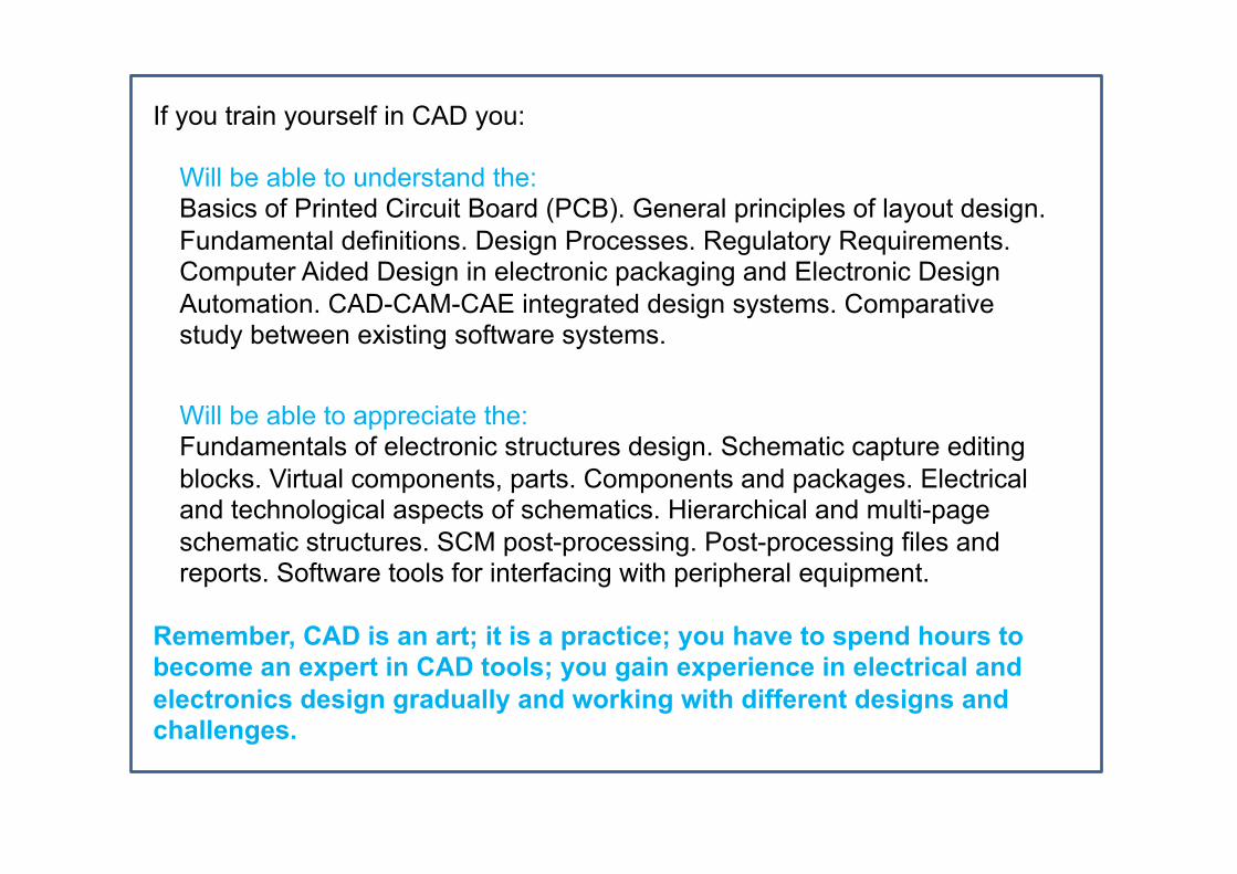
Will be able to understand the: Basics of Printed Circuit Board (PCB). General principles of layout design. Fundamental definitions. Design Processes. Regulatory Requirements. Computer Aided Design in electronic packaging and Electronic Design Automation. CAD-CAM-CAE integrated design systems. Comparative study between existing software systems.
If you train yourself in CAD you:
Will be able to appreciate the: Fundamentals of electronic structures design. Schematic capture editing blocks. Virtual components, parts. Components and packages. Electrical and technological aspects of schematics. Hierarchical and multi-page schematic structures. SCM post-processing. Post-processing files and reports. Software tools for interfacing with peripheral equipment.
Remember, CAD is an art; it is a practice; you have to spend hours to become an expert in CAD tools; you gain experience in electrical and electronics design gradually and working with different designs and challenges.

PCB design environments. Board density. Strategies for increasing the density - influences of pads, vias and trace widths on PCB density. Design capabilities: placing, routing, replacing and renaming strategies. Technological aspects regarding the optimum layout design. Multi-layer structures. Topological optimizations - virtual costs. "Back-annotation” method. High-frequency/high-speed board design. EMI problems during interconnection structure development. EMC of PCB/MCM modules. Electromagnetic compatibility (EMC), thermal analysis, simulation-both electrical and thermal and importantly, signal integrity analysis (SIA) at board level. Three important terms used in CAD of PWBs is:
Design for Manufacturing (DFM) Design for Reliability (DFR) & Design for Testability (DFT)
In a CAD package you can visualize:

Design for Manufacturing (DFM) - handshake between designers and manufacturers - bottlenecks in manufacturing - impossible specs in manufacturing cannot be designed - wastage of raw material can be minimised - high yield at lower costs
Design for Reliability (DFR)
- failures to be predicted by simulation - materials analysis is a must - physical properties of materials used in PWBs and inner layers - design for higher reliability- electrical and thermal - MTTF and MTBF to be understood (complex though) - current DFR mechanisms eliminate experimental verification
Design for Testability (DFT)
- ability to test the board efficiently after assembly - layout of board components become crucial - good understanding of components sizes, shapes, properties - efficient usage of electromechanical components, if used


