razorjr.files.wordpress.com file · web viewother virtual instruments in multisim include a word...
TRANSCRIPT

MULTISIM
CHAPTER 3: MULTISIM3.1 INTRODUCTION TO MULTISIMMultisim is a virtual electronic circuit design, analysis, and simulation programme that
design and analyse analogue, digital and mixed mode circuits on a PC using virtual
instruments. Virtual instruments are used to measure circuit behaviour such as voltage,
current, power, frequency and signals on a scope. They look just like real instruments
without fear of damaging the circuit components or the instruments.
The basic virtual instruments in Multisim are:
a) Multimeter
It measures resistance, ac/dc voltage and ac/dc current.
b) Function Generator
It produces sinewave, squarewave and triangular wave signals of adjustable
frequencies and amplitudes.
c) Wattmeter
It measures the power in watts consumed in a circuit.
d) Oscilloscopes (2-ch and 4-ch).
They display the traces of a peak-to-peak voltage signal in a circuit.
e) Bode Plotter
It produces a graph of the circuit’s frequency response. It is useful for
analysing electronic filter circuits.
f) Frequency Counter
It measures the frequency of an ac voltage signal.
Other virtual instruments in Multisim include a Word Generator, a Logic Analyzer,
a Logic Converter, an IV Analyzer, a Distortion Analyzer, a Spectrum Analyzer, a
Network Analyzer, a virtual Agilent Function Generator, Multimeter, and
Oscilloscope.

Types of electronic components that are available to build circuits in Multisim are:
a) DC and AC power sources, single phase and three phase
b) Resistors, resistor packs, potentiometers
c) Capacitors, single value and variable
d) Inductors, single value and variable
e) Switches, Connectors, Relays, Motors, Solenoids, Timers
f) Transformers
g) Diodes, LEDs, Zener
h) Transistors, NPN, PNP, JFET, MOSFET Operational Amplifiers, A-to-D and D-to-
A Converters
i) IC chips, 7400 TTL series, 4000 CMOS series
j) Lamps, LED indicators, Bar graphs
k) Voltage Regulators, Transducers, Crystals, Vacuum tubes, Fuses
l) And many more components in component libraries

3.2 INTRODUCTION TO MULTISIM INTERFACEMultisim user's interface is shown below:
Figure 1: Multisim user's interface
3.2.1 Design Bar
The design bar is central components of Multisim that guides user go through building,
simulating, analysing and exporting design.
The Component design button is selected by default.
The Component Editing allows user to add or modify the components in Multisim.
The Instrument design button is selected by default.
The Simulate button runs/stops/pauses the simulation. The green sine wave line
moves while the simulation is running.

The Analysis button allows user to choose the type of circuit analysis.
The Postprocessor allows user to perform further operation on the simulation
results.
The VHDL/Verilog HDL button allows user to work with VHDL modelling.
The Report button allows user to print the reports about circuit.
The Transfer button allows user to communicate with and convert to PCB layout
programme.
3.2.2 Controlling Circuit Display
Figure 2: Controlling Circuit Display

3.2.3 Components Toolbar
Figure 3: Components Toolbar
3.3 PLACING COMPONENTS3.3.1 Placing a Battery
Step 1: Place a Battery1. To place the first component (a 5 volt battery):
Place the cursor on the Sources Parts Bin button and click. The contents of the
Sources Parts Bin appear:

2. Click on the DC Voltage Source button and move your cursor to the circuit window.
Your cursor changes to indicate a part is ready to be placed.
3. Move to the top left corner of the circuit window to place the battery. Click in this
general area or, to be more precise, use the page borders as a guide and click in
the intersection of row A and column 1. The battery appears on your circuit
window:
Step 2: Change the Battery’s ValueBy default, the battery is a 12V battery, but our circuit calls for a 5V battery.
To change the battery’s value:
1. Double-click on the battery. The battery’s properties screen appears, with the Value tab
displayed.
2. Change the “12” to a “5” and click OK.

3.3.2 Placing a Resistor
Step 1: Place a ResistorTo place the first resistor:
1. Place your cursor on the Basic Parts Bin button and, from the toolbar that appears, click
the Resistor button. The Component Browser screen appears:
2. Scroll through the Component List to find the 100ohm resistor we need for our circuit.
3. Select the 100ohm resistor and click OK or double click on the component value. The
cursor will appear on the circuit window as a ghost image of the resistor.
4. Move your cursor to approximately A5 and click to place the component.

Step 2: Rotate the ResistorThe resistor needs to be rotated in order to set up conveniently into a circuit.
1. Right-click on the resistor. A pop-up menu appears.
2. Choose 90 Counter CW from the menu. The results look like this:
3.4 EDITING A BASIC SCHEMATIC WITH MULTISIM1. Click Tools Edit Components
2. From the Database Name list, the database of the component that needs to be edited can be chose.
3. From the Family Name list, the family of the component that needs to be edited can be chose.
4. From the Component Name list, the component that needs to be edited can be chose.5. To edit, click Edit (to cancel, click Exit).

3.5 VIRTUAL COMPONENTSThe instrument toolbar is displayed by default.
To choose any of the virtual components, click the Instruments button.
3.6 LOGIC GATES AND COMBINATIONAL CIRCUITSA combinational circuit consists of logic gates whose outputs at any time are determined
from the present combination of inputs. A combinational circuit performs an operation
that can be specified logically by a set of Boolean functions. A combinational circuit
comprises of input variables, logic gates and output variables.
3.6.1 The InverterOperation:
When the input is LOW, The output is HIGH; when the input is HIGH, the output is
LOW, thereby producing an inverted output pulse.
Symbol:
Truth Table:
INPUT (A) OUTPUT (Y)0 11 0
A Y

3.6.2 The AND GateOperation:
For a 2-input AND gate, output Y is HIGH if both input A and B are HIGH; Y is LOW if
either A or B is LOW, or both A and B are LOW.
Symbol:
Truth Table:
INPUT (A) INPUT (B) OUTPUT (Y)0 0 00 1 01 0 01 1 1
3.6.3 The OR GateOperation:
For a 2-input OR gate, output Y is HIGH if either input A or B is HIGH, or if both A and B
are HIGH; Y is LOW if both A and B are LOW.
Symbols:
Truth Table: INPUT (A) INPUT (B) OUTPUT (Y)
0 0 00 1 11 0 11 1 1
3.6.4 The NAND gateOperation:
For a 2-input NAND gate, output Y is LOW if input A and B are HIGH; Y is HIGH if either
A or B are LOW, or if both A and B are LOW.
Symbols:
AB
Y
AB
Y
AB
Y

Truth Table: INPUT (A) INPUT (B) OUTPUT (Y)
0 0 10 1 11 0 11 1 0
3.6.5 The NOR GateOperation:
For a 2-input NOR gate, output Y is LOW if either input A or B is HIGH, or if both A and
B are HIGH; Y is HIGH if both A and B are LOW.
Symbols:
Truth Table:INPUT (A) INPUT (B) OUTPUT (Y)
0 0 10 1 01 0 01 1 0
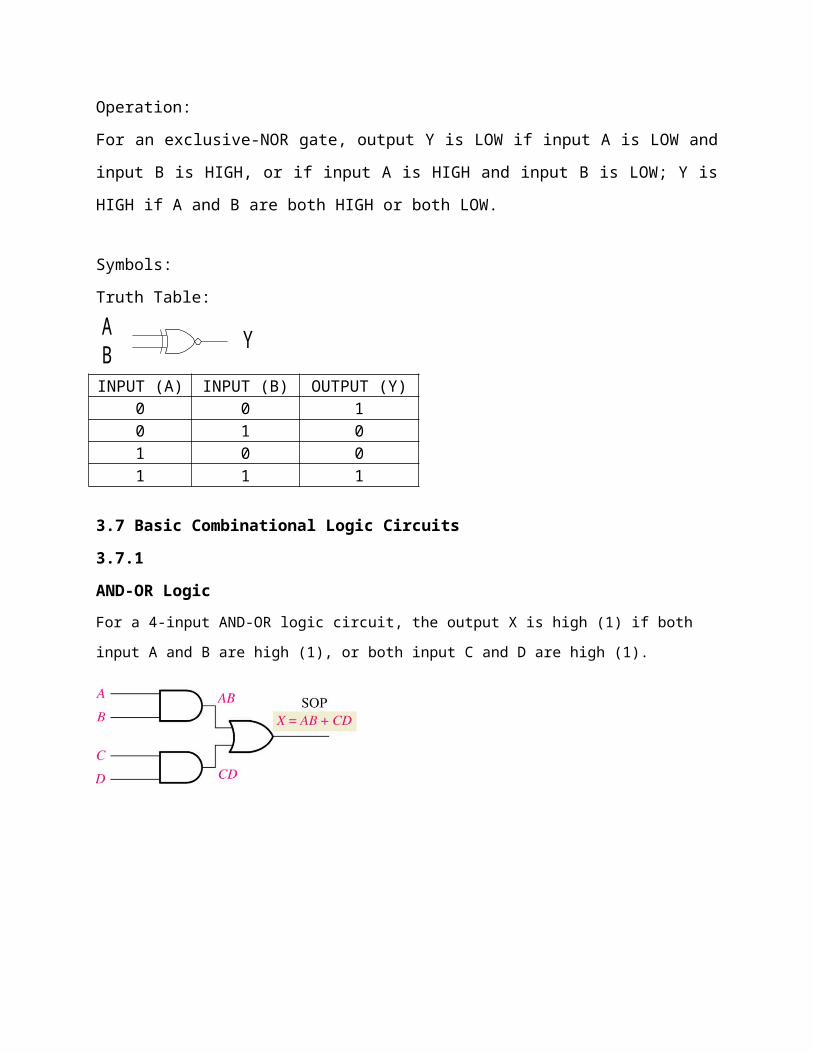
3.6.6 The XOR GateOperation:
For an exclusive-OR gate, output Y is HIGH if input A is LOW and input B is HIGH, or if
input A is HIGH and input B is LOW; Y is LOW if A and B are both HIGH or both LOW.
Symbols:
Truth Table: INPUT (A) INPUT (B) OUTPUT (Y)
0 0 00 1 11 0 11 1 0
3.6.7 The XNOR GateOperation:
AB
Y
AB
Y

For an exclusive-NOR gate, output Y is LOW if input A is LOW and input B is HIGH, or if
input A is HIGH and input B is LOW; Y is HIGH if A and B are both HIGH or both LOW.
Symbols:
Truth Table: INPUT (A) INPUT (B) OUTPUT (Y)
0 0 10 1 01 0 01 1 1
3.7 Basic Combinational Logic Circuits3.7.1AND-OR LogicFor a 4-input AND-OR logic circuit, the output X is high (1) if both input A and B are high (1), or
both input C and D are high (1).
3.7.2 AND-OR-Invert Logic
AB
Y

For a 4-input AND-OR-Invert logic circuit, the output X is LOW (0) if both input A and
input B are HIGH (1) or both input C and input D are HIGH (1)
3.7.3 Exclusive-OR Logic
3.7.4 Exclusive-NOR Logic
3.8 Functions of Combinational Logic

3.8.1 Multiplexer
A multiplexer is a device that allows digital information from several sources to be
routed onto a single line for transmission over that line to a common destination.
The basic multiplexer has several data-input lines and a single output lines.
Below is the logic symbol for a 4-input multiplexer (MUX). There are two data-
select lines because with two select bits, any one of four data-input lines can be
selected.
A 2-bit code on the data-select (S) input will allow the data on the selected data
input to pass through to the data output as table below:Data-select Inputs
Input selectedS1 S0
0 0 D0
0 1 D1
1 0 D2
1 1 D3
The data output is equal to the state of the selected data input
The total expression for the data output is
Y = D0S1’S0’ + D1S1’S0 + D2S1S0’ + D3S1S0
This can be implemented by the circuit below:

Because the data can be selected from any one of the input lines, this circuit is
also referred to as a data selector The select bits of multiplexer depend on the data input, 2n.
3.8.2 Demultiplexer
The DEMUX is a reverse multiplexer function.
It takes digital information from one line and distributes it to a given number of
output lines.
It is known as data distributors.
Below is the 1-line-to-4-line demultiplexer circuit.
The data input line goes to all of the AND gates.
The two data-select lines enable only one gate at a time and the data appearing
on the data-input online will pass through the selected gate to the associated
data-output line
3.8.3 Decoder
A decoder is a logic circuit that accepts a set of inputs that represents a binary
number and activates only the output that corresponds to that input number.
An AND gate can be used as a basic decoding element because it produces a
HIGH output only when all inputs are HIGH.
As example, to decode a binary number, 1001, make sure that all the inputs to
the AND gate are HIGH:
If a NAND gate is used in place of AND gate, a LOW output will indicate the
presence of the proper binary code
Below is the diagram of a general decoder with N inputs and M outputs:
N inputs M outputs
2N input codes only one output is high for eachinput code
Since each of the N inputs can be either 0 or 1, there are 2N possible input
combinations or codes. For each of these input combinations only one of the M
outputs will be active (HIGH); all other outputs are LOW.
In order to decode all possible combinations of 4-bits, 16 decoding gates are
required (24 = 16). This type of decoder is called a 4-line-to-16-line decoder
(because there 4 inputs and 16 outputs) or a 1-of-16-decoder (because for any
given code on the inputs, one of the 16 is activated).
An AND gate can be used to produce active-HIGH outputs and NAND gate to
produce active-LOW output.
Below is the logic symbol for a 4-line-to16-line decoder with active-LOW output.
The BIN/DEC label indicates that a binary input makes the corresponding
decimal output active. The input labels 8,4,2,1 represent the binary weights of the
input bits.
Decoder

Some decoders have one or more ENABLE inputs that are used to control the
operation of the decoder. With the ENABLE line held HIGH, the decoder will
function normally. With ENABLE held LOW, all the outputs will be forced to the
LOW state regardless of the levels at the inputs. Thus, the decoder is enabled
only if ENABLE is HIGH.
3.8.3.1 BCD –to- Decimal Decoder
The BCD-to-decimal decoder converts each BCD code into one of the 10
position decimal digit indications.
This decoder also is preferred as a 4-line-to-10-line decoder or a 1-of-10-line
decoder.

Only 10 decoding gates are required because the BCD code represent only 10
decimal digits, 0-9.
For input combinations that are invalid BCD, none of the output will be activated.
The BCD-to-7-Segment Decoder- accepts the BCD code on its input and
provides outputs to drive-7-segment display devices to produce a decimal
readout.
3.8.4 Encoder
An encoder accepts an active level on one of its inputs representing a digit, such as
decimal or octal digit, and converts it to a coded output, such as BCD or binary
The process of converting from familiar symbols or numbers to a coded format is
called encoding.
3.8.4.1 The Decimal-to-BCD Encoder
This type of encoder has 10 inputs- one for each decimal digit- and four output
corresponding to the BCD code as below:
This is 10-line-to-4-line encoder
Decimal Numbers BCDA3 A2 A1 A0
0123456789
0 0 0 0 0 0 0 1 0 0 1 0 0 0 1 1 0 1 0 0 0 1 0 1 0 1 1 0 0 1 1 1 1 0 0 0 1 0 0 1

Refer to the table above, the MSB of BCD code; A3 is always a 1 for decimal digit
8 or 9. An OR expression for bit A3 in terms of decimal digits: A3 = 8 + 9
Bit A2 is always 1 for decimal digit 4, 5, 6, 7 and can be expressed as an OR
functions as: A2 = 4+5+6+7
A1 = 2+3+6+7
A0 = 1+3+5+7+9
To implement the logic circuitry required to encoding each decimal digit to a BCD
code as follows:
When HIGH appears on one of the decimal digit input lines, the appropriate
levels occur on the four BCD output lines.
As example, if line 9 is HIGH this condition will produce a HIGH on outputs A0
and A3 and LOW on outputs A1 and A2, which is the BCD code (1001) for decimal
9.
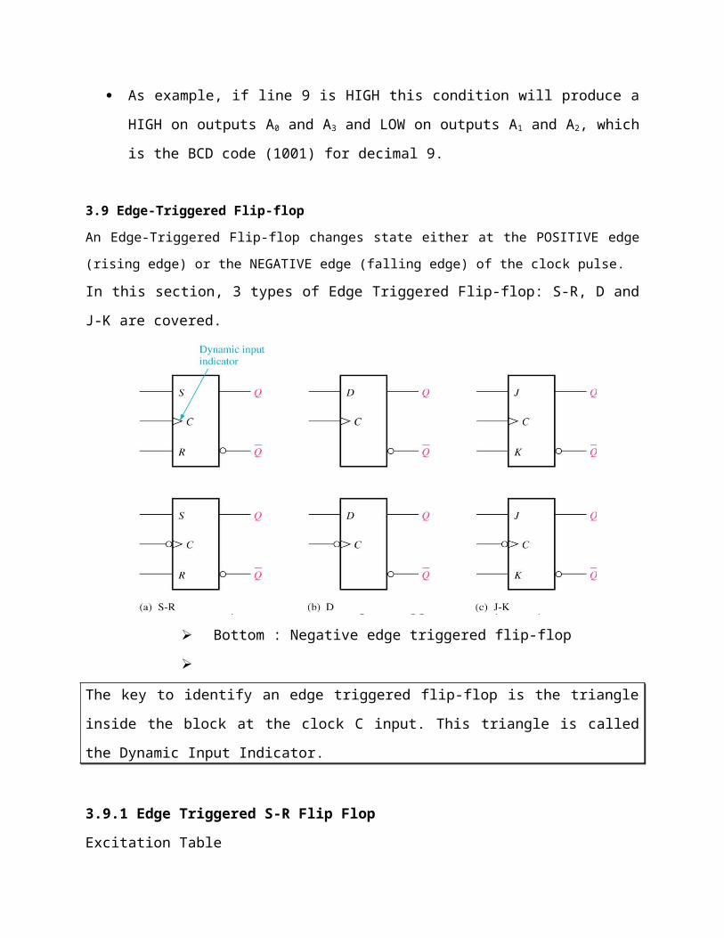
3.9 Edge-Triggered Flip-flopAn Edge-Triggered Flip-flop changes state either at the POSITIVE edge (rising edge) or the
NEGATIVE edge (falling edge) of the clock pulse.
In this section, 3 types of Edge Triggered Flip-flop: S-R, D and J-K are covered.

Top : Positive edge triggered flip-flop
Bottom : Negative edge triggered flip-flop
The key to identify an edge triggered flip-flop is the triangle inside the block at the clock
C input. This triangle is called the Dynamic Input Indicator.
3.9.1 Edge Triggered S-R Flip FlopExcitation Table
Input S Input R Input CLK Output Q Comments0 0 NC No Change0 1 0 RESET1 0 1 SET1 1 X Invalid
Timing Diagram

3.9.2 Edge Triggered D Flip FlopExcitation Table
Input D Input CLK Output Q Comments0 0 SET1 1 RESET
Q follows D at the triggering clock edge.
Timing Diagram
3.9.3 Edge Triggered J-K Flip FlopExcitation Table
Input J Input K Input CLK Output Q Comments0 0 NC No Change0 1 0 RESET1 0 1 SET1 1 Q Toggle.
Q is the prior output before clock transition.
Toggle Operation – When both inputs are HIGH, the output changes to the
opposite state on each successive clock spike (J=1, K=1, Q=1 and 0 repetitively).
A J-K flip-flop connected for toggle operation is sometimes called T flip-flop.
The functioning of J-K flip-flop is similar to S-R flip-flop except that J-K has no
invalid state.
Timing Diagram


LAB 3: COMBINATIONAL LOGIC CIRCUIT1.0 Objectives
At the end of this lab session, you should be able to:
explain the logic gates and combinational circuits.
construct combinational circuit in Multisim by using Logic Converter.
design a combinational circuit in Multisim.
2.0 Logic Tools in Multisim
Figure L3-1
One of the virtual instruments in Multisim is the Logic Converter. The arrow in the figure
L3-1 above shows the Logic Converter button.
Logic Converterbutton
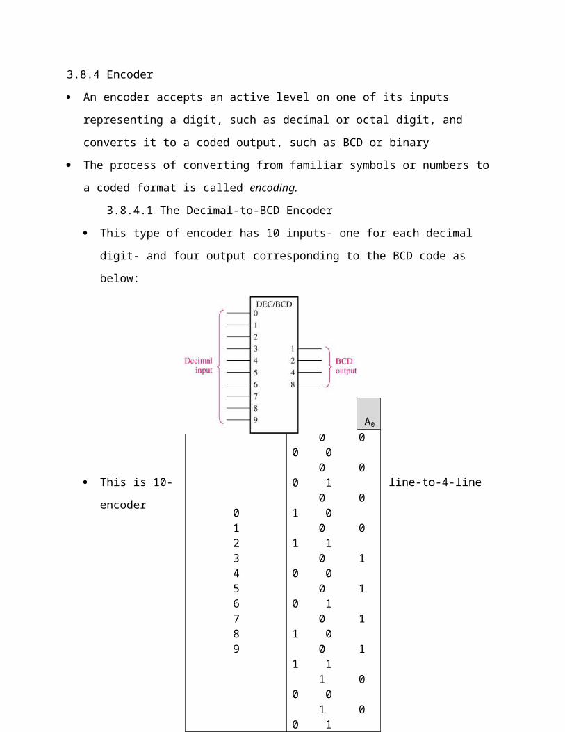
Figure L3-2
When the Logic Converter button is clicked, the logic converter symbol is shown in the
figure L3-2 above.
Logic Converter

Figure L3-3
In the logic converter, most of the logic conversions needed is there. For example, if we
want to obtain a circuit for the following Boolean expression,
Firstly, enter the Boolean expression into the logic converter as below:
Then, click on the Boolean expression truth table conversions option:
Next, the Boolean expression can be simplified by clicking (Note that
for this example, the Boolean expression cannot be simplified anymore).
Finally, click to generate the combinational circuit which shown in figure
L3-4 below.
Truth table
Truth table conversion
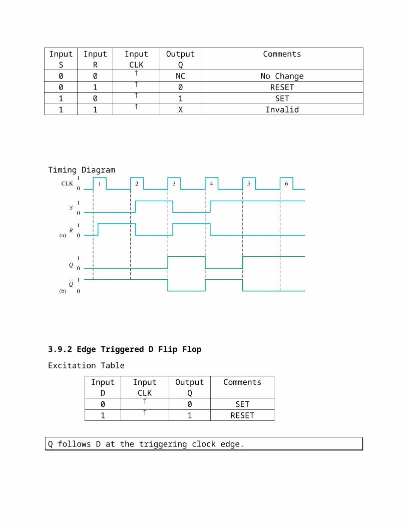
Figure L3-4
3.0 Exercise
1. Construct a three-input combinational circuit for f = m (2, 4, 5, 7) with the aid of Multisim.
Show and explain all the steps in details.
2. Design a four-input combinational circuit for f = m (0, 2, 4, 6, 9, 12, 14) with the aid of
Multisim. Show and explain all the steps in details.
3. AB represents a two-bit binary number that can have any value (00, 01, 10, or 11); for
example, when A = 1 and B = 0, the binary number is 10, and so on. Similarly, CD
represents another two-bit binary number. Design a logic circuit, using A, B, C, and D inputs,
whose output will be HIGH whenever two binary numbers AB are equal and greater than CD. It is impossible for inputs AB and CD to be HIGH at the same time.
a) Draw the logic circuit from the simplified Boolean expression (use AND, OR and
NOT gates).
b) Draw the logic circuit from the simplified Boolean expression (use NAND gates).
Circuit is generated