張所鋐 國立台灣大學機械工程系所教授 奈米 機電系統研究中心主任...
DESCRIPTION
奈米操控技術. 張所鋐 國立台灣大學機械工程系所教授 奈米 機電系統研究中心主任 [email protected]. 48 粒鐵原子在銅基板上形成的量子圍欄 (Quantum Corral of 48 Fe Atoms on Cu). 利用 STM 形成的步驟. 量子圍欄形成 7.3 nm 半徑圓環. IBM Almaden Research Center. 奈米科技的大事紀. 1959 美國 Prof. Richard Feynman 概念 1974 日本谷口教授使用 nanotechnology - PowerPoint PPT PresentationTRANSCRIPT
台大奈米機電系統研究中心 http://nems.ntu.edu.tw
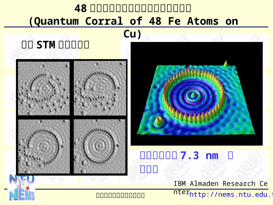
48 粒鐵原子在銅基板上形成的量子圍欄(Quantum Corral of 48 Fe Atoms on Cu)
利用 STM 形成的步驟
量子圍欄形成 7.3 nm 半徑圓環
IBM Almaden Research Center

台大奈米機電系統研究中心 http://nems.ntu.edu.tw
奈米科技的大事紀
1959 美國 Prof. Richard Feynman 概念1974 日本谷口教授使用 nanotechnology1981 IBM 發明掃瞄穿隧顯微鏡 (STM)1991 日本飯島澄男發現奈米碳管2000 美國柯林頓總統宣佈國家奈米計劃2003 我國國家奈米科技計劃開始

台大奈米機電系統研究中心 http://nems.ntu.edu.tw
由微機電、奈米機電演進至奈米技術
MEMS
NEMS
Nano-technology
MolecularElectronics

台大奈米機電系統研究中心 http://nems.ntu.edu.tw
各種顯微術比較

台大奈米機電系統研究中心 http://nems.ntu.edu.tw
http://www.park.com/
掃描探針顯微鏡 (SPM)
10 nm高深寬比型微探針
生物學( 生物檢體檢
測 )
記錄媒體業( 碟片記錄點檢測 )
材料科學( 材料表面結構分析 )

台大奈米機電系統研究中心 http://nems.ntu.edu.tw
\\\
Ernst Ruska Gerd Binnig Heinrich Rohrer
1/2 of the prize 1/4 of the prize 1/4 of the prize
Federal Republic of Germany
Federal Republic of Germany
Switzerland
Fritz-Haber-Institut der Max-Planck-Ges
ellschaft Berlin, Federal Repu
blic of Germany
IBM Zurich Research Laboratory
R chlikon, Switzerland
IBM Zurich Research Laboratory
R chlikon, Switze\rland
b. 1906d. 1988
b. 1947 b. 1933
1986 Nobel Prize in Physics: STM

台大奈米機電系統研究中心 http://nems.ntu.edu.tw
掃瞄穿隧式顯微鏡 (STM)
穿隧電流感測器示意圖
壓電平台
電壓源
d
試片
微探針導電
高剛性
精密電流計
It
VI
ON
It V e (-Cd)
It :穿隧電流
V :施加於探針和試片間的偏壓
C :材料常數
d:探針和試片間的間距
STM 鎢針

台大奈米機電系統研究中心 http://nems.ntu.edu.tw
IBM Spelled with Xenon Atoms

台大奈米機電系統研究中心 http://nems.ntu.edu.tw
原子力顯微鏡 (AFM)
試片
CCD鏡組
聚焦鏡
雷射二極體
光檢測器
分光鏡微探針
反射鏡聚焦鏡

台大奈米機電系統研究中心 http://nems.ntu.edu.tw
AFM Cantilever-type 探針
•Tip Radius•Aspect Ratio•Stiffness•Cantilever•電性•磁性
10 nm高深寬比型微探針金字塔型微探針
W
d
L
(a)探針尖端外形示意圖 (b)以不同探針外形掃瞄相同輪廓試片之結果比較圖
掃瞄影像試片探針
掃瞄影像試片探針
W
d
L
(a)探針尖端外形示意圖 (b)以不同探針外形掃瞄相同輪廓試片之結果比較圖
掃瞄影像試片探針
掃瞄影像試片探針
W
d
L
(a)探針尖端外形示意圖 (b)以不同探針外形掃瞄相同輪廓試片之結果比較圖
掃瞄影像試片探針
掃瞄影像試片探針

台大奈米機電系統研究中心 http://nems.ntu.edu.tw
微機電多頭探針陣列
Nanotechnology 13 (2002) 212–217
SEM 放大圖,擁有陣列式 32支 DPN 探針。左下角為針尖的放大圖。探針材料為 Si3N4 ,以 LPCVD 製成;尺寸 400 um x 50 um ,厚度 600 nm 。
SEM 放大圖,擁有陣列式 8支 DPN 探針。左下角為針尖的放大圖。針尖的曲度半徑是 100 nm
探針材料為 Si 晶體;尺寸 1400 um x 15 um ,厚度 10 um。

台大奈米機電系統研究中心 http://nems.ntu.edu.tw
1982 Scanning Tunneling Microscopy (STM)
--- G. Binnig, H. Rohrer et al, (1982)
1982 Near-Field Scanning Optical Microscopy (
NSOM)
--- D. W. Pohl (1982)
1986 Atomic Force Microscopy (AFM)
--- G. Binnig, C. F. Quate, C. Gerber (1986)
1986 Scanning Thermal Microscopy (SThM)
1987 Magnetic Force Microscopy (MFM)
1987 Friction Force Microscopy (FFM or LFM)
1988 Electrostatic Force Microscopy (EFM)
1989 Scanning Capacitance Microscopy (SCM)
1991 Force Modulation Microscopy (FMM)
掃描探針顯微鏡 (Scanning Probe Microscope)

台大奈米機電系統研究中心 http://nems.ntu.edu.tw
資訊儲存指標 (Data storage Roadmap)
IBM J. Res. Develop. 44(3), 3 May 2000
Millipede
Atom surface density
Non magnetic storage

台大奈米機電系統研究中心 http://nems.ntu.edu.tw
AFM 操控 : IBM Millipede 資料儲存裝置IBM 已經製作出了 32x32 陣列的原型, 92x92 um pitch at 3x3 mm chip ,儲存密度達 400 Gb/inch2 ,預估將可達 1 Tb/inch2 ,如郵票的面積即可儲存相當於 25 片 DVD 的容量。
Appl. Phys. Lett., 77, 2000, pp. 3299-3301.
1,024 AFM Tip Array

台大奈米機電系統研究中心 http://nems.ntu.edu.tw
IBM Millipede 資料儲存裝置
• 機構的作動方式是利用電阻加熱, 同時讓懸壁樑彎曲使 AFM 探針向 PMMA方向移動以及加熱 AFM 探針。
•全結構皆使用微 / 奈米機電製程製作,在矽基材上,植上所需的平面結構形狀,最後,再使用非等向性蝕刻技術,將平面結構從矽基材上釋放成為一懸壁樑結構。寫入時,需將探針加熱到 500~700oC 。
•寫入凹洞後的 PMMA ,如左圖所示,圖中( a )的大小約為 40 nm ,間距為 120 nm , PMMA 厚度為 70 nm ,圖 (b) 的凹洞密度約為 400 Gb/inch2 ,圖( c )為超高資料密度,其密度達到 1 Tb/in2 。
Appl. Phys. Lett., 77, 2000, pp. 3299-3301.
不同儲存密度下, PMMA 上的凹洞分佈

台大奈米機電系統研究中心 http://nems.ntu.edu.tw
用於操作奈米鉗子的矽懸梁臂基座。Ti/Pt 薄層覆在針尖並連接於懸梁臂上的鋁線。利用聚焦離子束將 Ti/Pt 薄層分割成兩段,並分別連接兩條鋁線。
SEM 輔助 AFM 奈米碳管鉗子操作(CNT Nano-tweezers assembled in SEM, operated in AFM)
APL, 79 (11), 9/2001
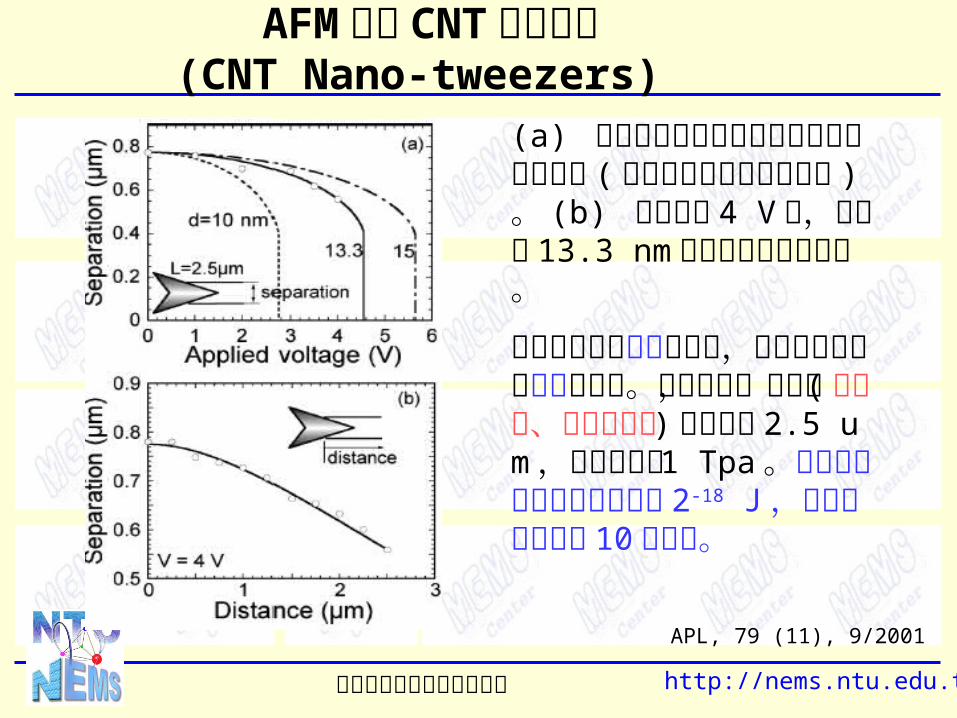
奈米碳管長 2.5 um ,初始空隙為 780 nm (a) ,靜電力於 4.5 V 時空隙為零 (d) 。
台大奈米機電系統研究中心 http://nems.ntu.edu.tw
(a) 施加的電壓與奈米鉗子兩端距離的關係圖 ( 列出三種不同直徑的碳管 )。 (b) 在電壓為 4 V 下,直徑為 13.3 nm 的奈米碳管的彎曲度。
開迴路表示其實驗的結果,點及實線表示其計算的結果。在計算中,碳管臂( 有彈性、規律且連續 ) 的長度為 2.5 um ,楊式係數為 1 Tpa 。碳管間的凡得瓦力估計值為 2-18 J ,比彎曲能量要小 10倍之多。
AFM 下的 CNT 奈米鉗子(CNT Nano-tweezers)
APL, 79 (11), 9/2001

台大奈米機電系統研究中心 http://nems.ntu.edu.tw
奈米操控系統• UNC 的奈米操控系統
– AFM– Graphics engine/interface– Phantom force stylus
資料來源: www.cs.unc.edu

台大奈米機電系統研究中心 http://nems.ntu.edu.tw
雲母基底上多層奈米碳管(MWCNT) 的操控。碳管長 800 nm ,直徑 13 nm。碳管雖受到強大的應變,卻沒有斷裂。
奈米碳管的操控
Microsc. Microanal. 4, 504–512, 1999
單層的奈米碳管束 (SWCNT) ,長 800 nm ,直徑 15 nm。利用 AFM 針尖將其扳彎時,它顯現出比多層奈米碳管 (MWCNT) 小的剛性。
台大奈米機電系統研究中心 http://nems.ntu.edu.tw
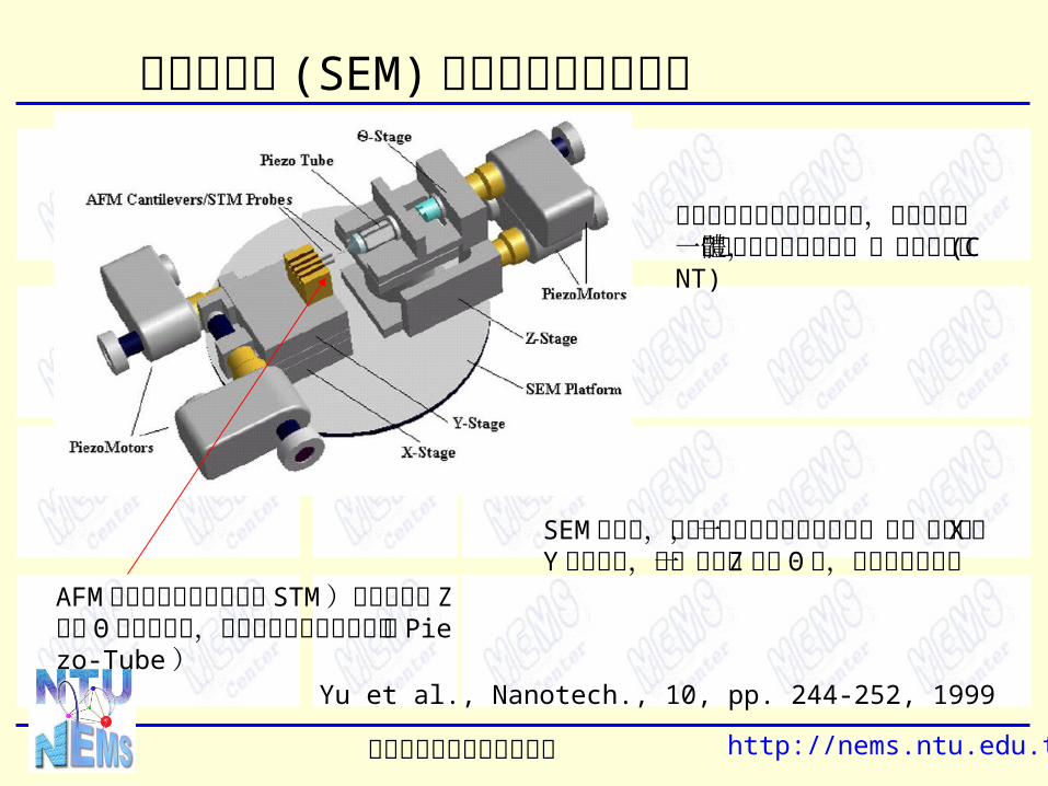
SEM 平台上,裝設有兩組致動器移動平台,其一組含有 X 與 Y軸移動台,另一組含有 Z軸與 Θ軸,於二組移動台上
電子顯微鏡 (SEM)輔助之奈米操控應用
AFM或穿遂式掃瞄顯微鏡( STM )探針,其中 Z軸與 Θ軸移動台中,又裝設有管狀壓電致動器( Piezo-Tube ) Yu et al., Nanotech., 10, pp. 244-252, 1999
這種原型機器可探測和操控,也可以處理一個被選定的奈米級物體,像奈米碳管 (CNT)

台大奈米機電系統研究中心 http://nems.ntu.edu.tw
電子顯微鏡 (SEM)輔助之 AFM 操控奈米碳管
多層奈米碳管藉由電弧加工成長在探針上,和利用空氣氧化純淨奈米碳管,另外單層奈米碳管則是利用其他方法,多層奈米碳管的直徑為 2~ 50 nm ,而其長為 10 μm
圖 a 是從一束的奈米碳管抽出一支奈米碳管附著在 AFM的針尖上的 SEM 的圖 圖 b 是有一束強硬的奈米碳管附著在 AFM 針尖上
圖 c 是奈米碳管連接在上下兩個針尖之間
圖 d 是一根奈米碳管連接在兩個AFM 碳針的旁邊
Yu et al., Nanotech., 10, pp. 244-252, 1999

台大奈米機電系統研究中心 http://nems.ntu.edu.tw
• 奈米碳管在各種共振模態時的共振情形• 振動頻率和奈米碳管的直徑 (D) 、長度 (L) 、密
度 (ρ) 、彎曲模數 (Eb) 有關
J. of Phys. and Chem. of Solids, 61(2000), 1025-1030
奈米碳管的共振
台大奈米機電系統研究中心 http://nems.ntu.edu.tw
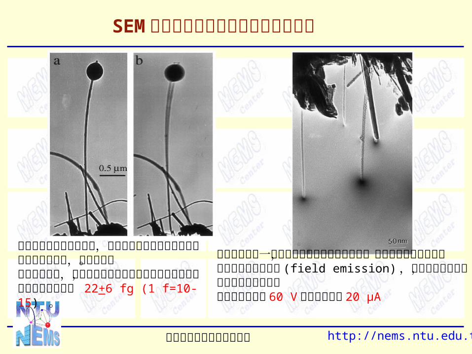
SEM 觀察奈米天平及電場放電發光現象
此為世界上最微小的天平,此種技術可以應用在測量大的生物和生醫分子,如病毒等。量測振動頻率,可以知道掛在奈米碳管末端的粒子質量,可量測質量可以到 22+6 fg (1 f=10-15) 。
奈米碳管的獨一無二結構特性顯示出在電場中,能產生高密度放電電流 奈米碳管在電場放電 (field emission) ,會有發光的現象,如圖中下方位置所示圖中施加電壓為 60 V ,放出電流約 20 μA
台大奈米機電系統研究中心 http://nems.ntu.edu.tw
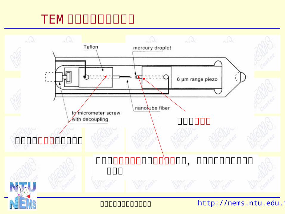
右側由壓電致動器移動水銀液滴裝置,使其與奈米碳管的自由端接觸
TEM輔助之奈米操控裝置
左端利用鐵弗龍夾具來固定
右端為自由端
台大奈米機電系統研究中心 http://nems.ntu.edu.tw
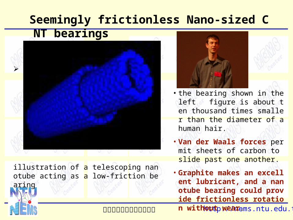
Seemingly frictionless Nano-sized CNT bearings
illustration of a telescoping nanotube acting as a low-friction bearing
• the bearing shown in the left figure is about ten thousand times smaller than the diameter of a human hair.
• Van der Waals forces permit sheets of carbon to slide past one another.
• Graphite makes an excellent lubricant, and a nanotube bearing could provide frictionless rotation without wear.

台大奈米機電系統研究中心 http://nems.ntu.edu.tw
Experiments performed inside the 100KV TEM using nano-manipulator.
(A to C) The process of opening the end of a MWNT (A), exposing the core tubes (B), and attaching the nanomanipulator to the core tubes (C). (D and E) Two different classes of subsequent experiments performed. In (D), the nanotube is repeatedly telescoped while observations for wear are performed. In (E), the core is released and pulled into the outer-shell housing by the attractive van der Waals force.
Low-Friction Nanoscale Linear Bearing Realized from Multiwall Carbon Nanotubes
A TEM image of a peeling and shaped (2.9 V and 200 micro-amp) telescoped nanotube.This particular nanotube originally had nineshells, but upon telescoping a four-shell core has been nearly completely extracted.

台大奈米機電系統研究中心 http://nems.ntu.edu.tw
Use of nano-manipulator in TEM
In the first five frames, the core nanotubes are slowly withdrawn to the right.
In the sixth image, which occurred one video frame after the core was released, the core has fully retracted into the outer nanotube housing as a result of the attractive van der Waals force.
Low-Friction Nanoscale CNT Linear Bearing

台大奈米機電系統研究中心 http://nems.ntu.edu.tw
(A) An as-grown bamboo section.(B) The same area after the core tubes on the right have been telescoped outward. Bamboo sections are independent and are free to slide inside their nanotube housing. Static friction force: 2.3 x 10E-14 N per atom (6.6 x 10E-15 N/A2)
Dynamic friction force: 1.5 x 10E-14 N per
atom (4.3 x 10E-15 N/A2) : near perfect surface
Low-Friction Nanoscale Multiwall Carbon Nanotubes Linear Bearing
TEM images of a bamboo section of a MWNT.
Conventional measured friction force is three order magnitude greater.
台大奈米機電系統研究中心 http://nems.ntu.edu.tw
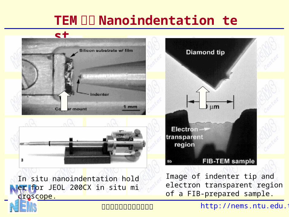
Image of indenter tip and electron transparent region of a FIB-prepared sample.
TEM 輔助 Nanoindentation test
In situ nanoindentation holder for JEOL 200CX in situ microscope.

台大奈米機電系統研究中心 http://nems.ntu.edu.tw
TEM images of contacting STM tip
Nature, 395, pp.781, 1998
A gold bridge formed between the gold tip (top) and gold substrate
(bottom).

台大奈米機電系統研究中心 http://nems.ntu.edu.tw
Quantized conductance of gold atom contact
Nature, 395, pp.781, 1998
台大奈米機電系統研究中心 http://nems.ntu.edu.tw
Challenges: novel nano components functional components connect nano to maco to macro, build connection network grow components at contacts at connectors molecular recognition for contacting explore interface functionality, self assembly material process beyond Si
Do Nano Science & Technology in Nature’s Way
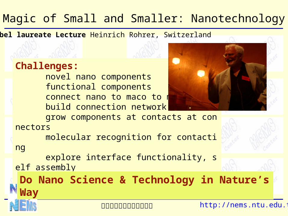
Nobel laureate Lecture Heinrich Rohrer, Switzerland
The Magic of Small and Smaller: Nanotechnology

台大奈米機電系統研究中心 http://nems.ntu.edu.tw
Superlattices: New Physics and Electronics
suggestion to become a Nobel winner: 1. do not allow yourself to be trapped by your
experiences 2. do not allow yourself to become overly attached to any authority in your field 3. do not hold on to what you don’t need 4. do not avoid confrontation 5. do not forget your spirit of childhood
Nobel Laureate Leo Esaki ( Tokyo, Japan )1973 Nobel Prize in Physics- tunneling in solids (a total of 3 person)Esaki diode, super lattice

台大奈米機電系統研究中心 http://nems.ntu.edu.tw
謝謝 !
敬請指教 !
Richard Feynman 於 1959 年 12月發表 : 『在原子級的世界中,我們將發現全新的力、全新的可能性、以及全新的效應。物質在加工與製造上所遇到的問題將與之前大相逕庭。』