© 2012 karan bhagat - ideals
TRANSCRIPT

© 2012 Karan Bhagat

TUTORIAL ON DESIGNING AND IMPLEMENTING A
DIRECT DIGITAL SYNTHESIZER (DDS) ON A
FIELD PROGRAMMABLE GATE ARRAY (FPGA)
BY
KARAN BHAGAT
THESIS
Submitted in partial fulfillment of the requirements
for the degree of Master of Science in Electrical and Computer Engineering
in the Graduate College of the
University of Illinois at Urbana-Champaign, 2012
Urbana, Illinois
Adviser:
Professor José E. Schutt-Ainé

ii
ABSTRACT
Many telecommunication applications require a fast switching, fine tuning and superior
quality sinusoidal signal source for their components. One such a frequency synthesizer is a
direct digital synthesizer (DDS).
This thesis work utilizes a design that aims to combine digital circuit design and electronic
communication knowledge, and apply them in a practical environment. It does so by providing a
tutorial on designing and implementing a DDS on an FPGA using Xilinx’s ISE software. The
thesis also examines the final results and shows the unwanted spurs that are generated.
Since this is purely a digital design, it does not implement a digital-to-analog converter
(DAC) or a low-pass filter. Using a Virtex 6 design for the FPGA, one can achieve close to
perfect sinusoids, without any phase change, with varying frequency tuning words (FTWs).

iii
To my family, for their love, support, motivation and patience.
To my adviser, for his support, guidance and advice.
To my fellow student coworkers, for their advice and assistance.

iv
ACKNOWLEDGMENTS
I would like to thank my graduate school adviser, Professor José E. Schutt-Ainé, for all his
support and guidance over the past two and a half years. Thanks to Yuanwang Yang, who started
this project, helped design it, and from whom I took over the mantle. I thank Thomas Comberiate
for his continuous guidance and support on the subject. I thank Karnik Radadia for his immense
help on this project. I would also like to acknowledge James Hutchinson, the editor in the ECE
Publications Office, for his editing and advice on various formatting issues of this thesis.
Lastly, I would like to thank my parents, brother and sister-in-law for their continuous moral
support, motivation, understanding and patience throughout my education.

v
TABLE OF CONTENTS
Chapter 1. INTRODUCTION ....................................................................................................................... 1
1.1 Overview and Purpose ........................................................................................................................ 1
1.2 Outline................................................................................................................................................. 2
Chapter 2. FUNDAMENTALS AND BACKGROUND OF DDS .............................................................. 3
2.1 Structure and Theory of Operation ..................................................................................................... 3
2.2 Spurs in the DDS ................................................................................................................................ 5
Chapter 3. BACKGROUND IN VERILOG ................................................................................................. 7
3.1 Resources ............................................................................................................................................ 7
3.2 Necessary Knowledge for Designing a DDS ...................................................................................... 7
Chapter 4. FPGA DESIGN FLOW AND DESCRIPTION .......................................................................... 9
4.1 Design Flow ........................................................................................................................................ 9
4.2 Design Flow Description .................................................................................................................. 10
Chapter 5. FPGA DESIGN TUTORIAL .................................................................................................... 12
5.1 Functional/Device Specifications ..................................................................................................... 12
5.2 HDL Coding...................................................................................................................................... 13
5.3 Behavioral Simulation ...................................................................................................................... 20
5.4 Logic Synthesis ................................................................................................................................. 21
5.5 Gate-Level Simulation ...................................................................................................................... 23
5.6 Mapping, Placement and Route (PAR) ............................................................................................. 24
5.7 Static Timing Analysis (STA)........................................................................................................... 28
5.8 Post PAR Timing Simulation ............................................................................................................ 28
5.9 FPGA Configuration and Programming ........................................................................................... 28
5.10 Final Behavioral Simulations .......................................................................................................... 31
Chapter 6. DDS MEASUREMENTS ......................................................................................................... 34
6.1 Timing Reports ................................................................................................................................. 34
6.2 Behavioral and Post Map Simulations .............................................................................................. 34
6.3 Different Frequency Tuning Word (FTW) Cases ............................................................................. 35
Chapter 7. CONCLUSION AND FUTURE WORK .................................................................................. 37
References ................................................................................................................................................... 38
Appendix. CHOOSING A SIMULATOR AND SETTING UP MODELSIM ......................................... 40

1
Chapter 1. INTRODUCTION
1.1 Overview and Purpose
Frequency synthesis is an extremely important technology used in the field of
telecommunications. A direct digital synthesizer (DDS) plays a vital role in microwave/radio
frequency designs and projects that need a signal source which have no disturbances and little to
no noise. A DDS, similar to a numerically controlled oscillator (NCO), is used to generate a
sinusoid signal, or any other waveform of utmost clarity, that can switch frequencies very easily
and quickly. It is a partial digital design which can be easily designed and implemented and yet
provide a fine-tuning resolution.
In the field of electrical engineering, a DDS is usually preferred over an analog signal
generator for capabilities such as the following [1]:
1. Extremely fast frequency tuning while keeping the phase continuous with no overshoots
or undershoots
2. No need for manual tuning or tweaking with the accompanying redundancies
3. Digitally controlled environment that can be easily tested and reconfigured from
anywhere at any time
4. Frequency resolution in the micro-hertz range
5. Immunity to many ambient problems (e.g., temperature, dust between components,
dielectric presence, etc.)
The purpose of this thesis is to help design such a DDS on an FPGA. With the growing needs
of flexibility, extreme accuracy and effectiveness, FPGAs have started to play a very big role in
the domain of digital circuit design. FPGAs are generally similar to development boards that are
able to operate any circuit designed for them. They also have many switches and ports on the
board that help in testing and debugging. The biggest advantage of using an FPGA is that
designs can be created and changed over a very short period of time and unlike with application
specific integrated circuits (ASICs), the designer does not have to wait many months for the
circuit to be fabricated.

2
1.2 Outline
This thesis will serve as a complete tutorial that will provide background on a standard DDS
as well as explain how to design it in Verilog and implement it on an FPGA. Chapter 2 provides
insight into the fundamental and background knowledge behind the operation of a DDS,
additionally going over some of its drawbacks. Chapter 3 addresses the requirement of Verilog
coding in the field of circuit design. Apart from providing some resources, it also goes over some
necessary examples that are needed to design the DDS. Chapter 4 elaborates on the design flow
for designing circuits for an FPGA. Chapter 5 presents a detailed step-by-step tutorial on
designing, implementing and simulating the entire DDS on the FPGA. This chapter will utilize
Xilinx’s ISE software (which has many embedded tools) to facilitate all the three functions.
Chapter 6 shows the different results obtained when testing the DDS for different frequency
parameters. Finally, Chapter 7 concludes this thesis with a summary and ideas for future work.
3
Chapter 2. FUNDAMENTALS AND BACKGROUND OF DDS
This chapter covers the theory behind the design of a DDS and problems therein.
2.1 Structure and Theory of Operation
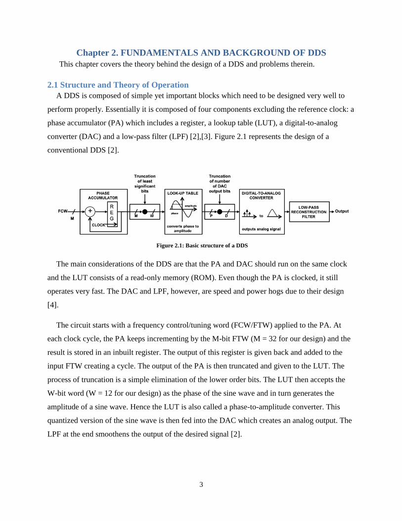
A DDS is composed of simple yet important blocks which need to be designed very well to
perform properly. Essentially it is composed of four components excluding the reference clock: a
phase accumulator (PA) which includes a register, a lookup table (LUT), a digital-to-analog
converter (DAC) and a low-pass filter (LPF) [2],[3]. Figure 2.1 represents the design of a
conventional DDS [2].
The main considerations of the DDS are that the PA and DAC should run on the same clock
and the LUT consists of a read-only memory (ROM). Even though the PA is clocked, it still
operates very fast. The DAC and LPF, however, are speed and power hogs due to their design
[4].
The circuit starts with a frequency control/tuning word (FCW/FTW) applied to the PA. At
each clock cycle, the PA keeps incrementing by the M-bit FTW (M = 32 for our design) and the
result is stored in an inbuilt register. The output of this register is given back and added to the
input FTW creating a cycle. The output of the PA is then truncated and given to the LUT. The
process of truncation is a simple elimination of the lower order bits. The LUT then accepts the
W-bit word (W = 12 for our design) as the phase of the sine wave and in turn generates the
amplitude of a sine wave. Hence the LUT is also called a phase-to-amplitude converter. This
quantized version of the sine wave is then fed into the DAC which creates an analog output. The
LPF at the end smoothens the output of the desired signal [2].
Figure 2.1: Basic structure of a DDS
4
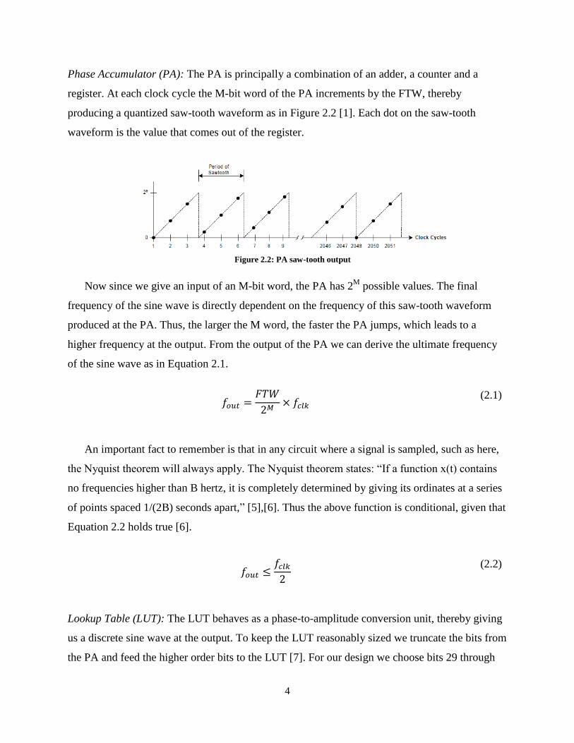
Phase Accumulator (PA): The PA is principally a combination of an adder, a counter and a
register. At each clock cycle the M-bit word of the PA increments by the FTW, thereby
producing a quantized saw-tooth waveform as in Figure 2.2 [1]. Each dot on the saw-tooth
waveform is the value that comes out of the register.
Now since we give an input of an M-bit word, the PA has 2M
possible values. The final
frequency of the sine wave is directly dependent on the frequency of this saw-tooth waveform
produced at the PA. Thus, the larger the M word, the faster the PA jumps, which leads to a
higher frequency at the output. From the output of the PA we can derive the ultimate frequency
of the sine wave as in Equation 2.1.
An important fact to remember is that in any circuit where a signal is sampled, such as here,
the Nyquist theorem will always apply. The Nyquist theorem states: “If a function x(t) contains
no frequencies higher than B hertz, it is completely determined by giving its ordinates at a series
of points spaced 1/(2B) seconds apart,” [5],[6]. Thus the above function is conditional, given that
Equation 2.2 holds true [6].
Lookup Table (LUT): The LUT behaves as a phase-to-amplitude conversion unit, thereby giving
us a discrete sine wave at the output. To keep the LUT reasonably sized we truncate the bits from
the PA and feed the higher order bits to the LUT [7]. For our design we choose bits 29 through
(2.1)
(2.2)
Figure 2.2: PA saw-tooth output
5
18 as the 12 bit W-word. This allows the hardware to be reasonably sized and not extremely
power hungry. The LUT will contain unique values of a sine wave over one period, however
even in that one period, the sine wave is symmetrical. To further exploit this symmetrical nature,
we can fill the table with values that correspond to only a quarter of a sine wave period [7].
For the FPGA design, one will need a coefficients file containing the values of the LUT.
Generate this file with the help of Matlab and store it as a ‘*.coe’. This file will then be added to
the ROM in Section 5.2, step 11.j.
Digital-to-Analog Converter (DAC): A second truncation process is carried out here, as the
output of the LUT is truncated to the appropriate number of bits and then given to the DAC. The
DAC creates an analog waveform from the discretized sine wave. An important fact to note here
is that the DAC is solely responsible for limiting the design’s maximum attainable frequency. It
does not matter how fast the PA is clocked as the DAC (which is one of two analog components
in the entire design) forms the bottleneck.
Low-pass Filter (LPF): The LPF behaves as a reconstruction filter that smoothens the signal
from the DAC. Since we do not want any aliases of the fundamental frequency, this LPF also
behaves as an antialiasing filter [1], thereby limiting us to the Nyquist frequency. Typically, a
Chebyshev filter is used to build this stage due to its sharp frequency response characteristics [1].
For the DDS design in this thesis, one need not implement a DAC and LPF because the
FPGA development board used for the design does not have those two components on board.
Hence we will simulate the behavior of the DAC using a different simulator in Section 5.8.
2.2 Spurs in the DDS
Due to the design’s inherent qualities, the generated sinusoid is not perfect and contains
certain disturbances/spikes/spurs [6].
Phase Truncation Spurs: To design a smaller sized LUT which draws less power, we eliminate
some of the least significant bits (LSBs) of the 32 bit word from the PA. This truncation of bits
leads to spectral impurity known phase truncation spurs and it is the biggest cause of noise and
spikes in the DDS system. Since this part of the system is completely digitally designed, there
are many algorithms that can be implemented to reduce these spurs.
6
Quantization Noise Spurs: In the DDS design presented here, we truncate the output of the LUT
even further and then give it to the DAC. The DAC, however, accepts a signed binary number
with a certain precision. To achieve this, the input bits are further rounded. This modification and
quantization leads to quantization noise spurs.
Quantization Nonlinearity Spurs: As the technical tutorial on DDS by Analog Devices states,
these spurs are a “consequence of the inability to design a perfect DAC” [1]. Due to the DAC’s
inherent design and non-ideal transfer function behavior, every input will have few errors
associated with it and thus one will not attain an ideal output. These errors, essentially caused by
the non-linearity of the DAC, lead to quantization nonlinearity spurs that can only be reduced by
increasing the precision of the DAC.

7
Chapter 3. BACKGROUND IN VERILOG
Digital circuits are designed and modeled using hardware description languages (HDLs).
Verilog and VHDL (very high speed integrated circuit HDL) are two such industry-standard
HDLs.
A beginner should design circuits in Verilog as VHDL has a higher learning curve and needs
to be more explicit when defining different modules.
3.1 Resources
1. The best resource for viewing examples of Verilog/VHDL files is the “World of ASIC” web
site [8]. It contains tutorials, examples, suggestions for different tools that are used with
digital design, lists of books to use as additional references, as well as some frequently asked
questions (FAQs).
2. Another good resource is a document titled “Verilog Tutorial” by Deepak Kumar Tala [9].
He is the same person who manages the web site mentioned in the previous point. This
tutorial goes over the design and tool flows, basic program designs, syntaxes and semantics,
operators, gate-level designs, behavioral modeling, writing test-benches, modeling finite state
machines (FSMs), etc.
3.2 Necessary Knowledge for Designing a DDS
Xilinx’s ISE tool (used in this project) contains many examples and tips on instantiating
models within a circuit. Section 5.2, step 5, of this tutorial will give instructions on accessing
those features.
Given below are some examples of code that will be necessary to use when designing the
DDS.
Registers and Wires: Many registers and wires will be needed for internal connections and
storages within the circuit design.
reg register_name; //single bit register
wire[11:0] wire_name //A 12-bit wide bus

8
Always blocks: To modify or perform certain functions recurrently or at a given time, use the
always instruction.
always@(posedge clk) //Used for only one instruction
clkout <= clk; //sending the clk signal to clkout at every positive edge of the clk
always #5 clk = ~clk; //changing the clk singal every 5ns
always@(posedge clk) //Begin and end constructs used when multiple operations
begin //need to be carried out
lowaddress <= address[17:0];
plusormunis <= address[31];
end
Initial statement: Used when one needs to execute a statement only once at the beginning of a
simulation [8]. This statement is very important for the test-bench file (Refer Section 5.2 step
13).
initial begin // Initialize Inputs
clk = 0;
en=1;
phasestep = 1048576;
end
Module and endmodule statement: The entire design for any module needs to be included within
these two constructs.
module dds(clk, phasestep,rom_en, data2DAC,clkout);
input clk;
input [31:0] phasestep;
output [12:0] data2DAC;
//Add remaining input and output ports.
//Add entire design and instantiations.
endmodule
9
Chapter 4. FPGA DESIGN FLOW AND DESCRIPTION
For a circuit designer there are typically two ways to design and implement digital circuits:
1. Application Specific Integrated Circuits (ASIC) Implementation
2. Field Programmable Gate Arrays (FPGA) Implementation
The main difference between the two is that in the case of FPGAs one can program a ready
development board and thus implement and test the design setup more quickly. ASICs, however,
are capable of a complete custom design [10], which makes them cheaper and smaller since the
device only contains components that are absolutely necessary to run the application.
From a research standpoint it is recommended to use an FPGA since one can easily modify
designs and test them using the numerous test switches and ports that are present on board.
Hence for this project a DDS will be implemented on an FPGA.
4.1 Design Flow
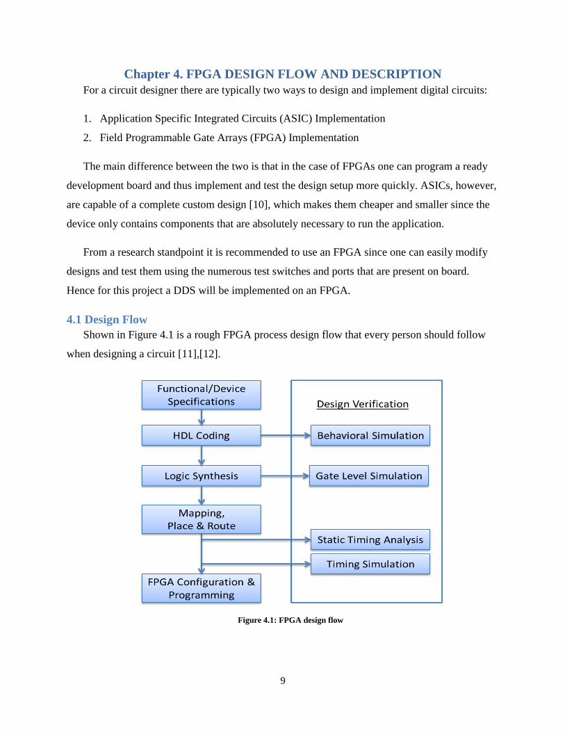
Shown in Figure 4.1 is a rough FPGA process design flow that every person should follow
when designing a circuit [11],[12].
Figure 4.1: FPGA design flow
10
4.2 Design Flow Description
Functional/Device Specifications: In this stage the designer is supposed to enter in the
configuration (make/model/speed/class/family) of the FPGA into the designing tool. The
designing tool then performs some preliminary setup to enable access to that particular FPGA
device’s intellectual properties (IPs), designs and components [13],[14].
Hardware Description Language (HDL) Coding: For this step, the designer codes his entire
design in a hardware readable language (Verilog or VHDL). The designer also has the option to
implement the project via a schematic based entry; however, when one needs to utilize
algorithms for the design, an HDL based entry is preferred [13],[14].
Logic Synthesis: Synthesis is a process that converts the HDL code into a gate-level netlist. This
netlist describes the different types of components, elements, interconnections between those
components and other necessary details like area occupied, temperature of operation, etc.
Another added feature of synthesis is that it checks the syntax of one’s code. In some cases it
also maps the design to the particular FPGA family that was selected in the Device
Specifications [13],[14].
In this tutorial, Xilinx’s ISE tool will use the embedded Xilinx Synthesis Technology (XST)
to perform the synthesis of the circuit. This tool goes through all the relevant processes, in
addition to generating a schematic view of the HDL [13],[14].
Mapping: This process maps the generic logic design (which is composed of different gates, flip
flops, modules and input/output switches) to the logic technology contained inside the chosen
FPGA device [13],[14].
Placement & Route (PAR): This phase is one of the most crucial steps in the entire
implementation. As the name suggests, the Placement is responsible for deciding where the
components should be placed within the FPGA. The Routing is then responsible for the
connections between those different components. PAR is extremely important because it is
performed around the designer’s timing and area constraints. As a result, a bad placement might
cause problematic routing, thereby leading to violations in the design [15].

11
FPGA Configuration and Programming/Implementation: This last phase of the FPGA design
flow incorporates loading the design onto the FPGA and then testing the circuit. This stage
converts the entire design into a ‘bitstream’ file which is loaded onto the development board.
Once loaded, the FPGA is ready to run with the designed circuit [15].
Design Verification: In every design it is extremely important to meet certain conditions and
satisfy important criteria at the end. Thus after every crucial designing step, the designer has to
test if the circuit meets those different constraints (e.g., functional logic, timing and area
stipulations) [15].
For this part Xilinx has given us the flexibility to choose its own internal tool, ISE Simulator
(ISim), or an external tool, ModelSim. Whenever we want, we can change our choice by right-
clicking on the topmost module within the view pane and then clicking on Design Properties
Simulator. The descriptions for each of the different testing stages are given below:
i. Behavioral Simulation: This stage is responsible for verifying the HDL functionality. It is
important to remember that this step only tests the code and not the gate-level
functionality [14].
ii. Gate-Level Simulation: Once the synthesis is completed and we have a gate-level netlist,
this simulation tests the timing and functionality of the circuit down to the gate design.
iii. Static Timing Analysis (STA): Once the PAR is completed and the STA is carried out,
the designer can analyze important aspects of the circuit like setup and hold times for the
circuit, critical paths within the circuit and clock skew rates. An STA traces through
every possible path in the circuit and can debug slow paths or glitches that could hamper
the circuit.
iv. Final Post-PAR Timing Simulation: This is the final timing simulation after PAR. This
simulation gives the designer an entire timing summary of the circuit, which is very close
to the actual results seen when implemented on the FPGA.
12
Chapter 5. FPGA DESIGN TUTORIAL
For your project you will use Xilinx’s ISE Design Suite. The ISE is a comprehensive tool
that allows the designer to initially describe the entire design and then perform other required
steps with the help of other tools. Think of it as a top-level tool that calls upon the other tools
when desired.
First and foremost you will need to download, from Xilinx’s web site, the latest ISE suite,
which is available on a freeware basis for a period of 30 days. Then open ISE by clicking on the
shortcut on the desktop or Start Menu Xilinx ISE Design Suite ISE Design Tools
Project Navigator.
5.1 Functional/Device Specifications
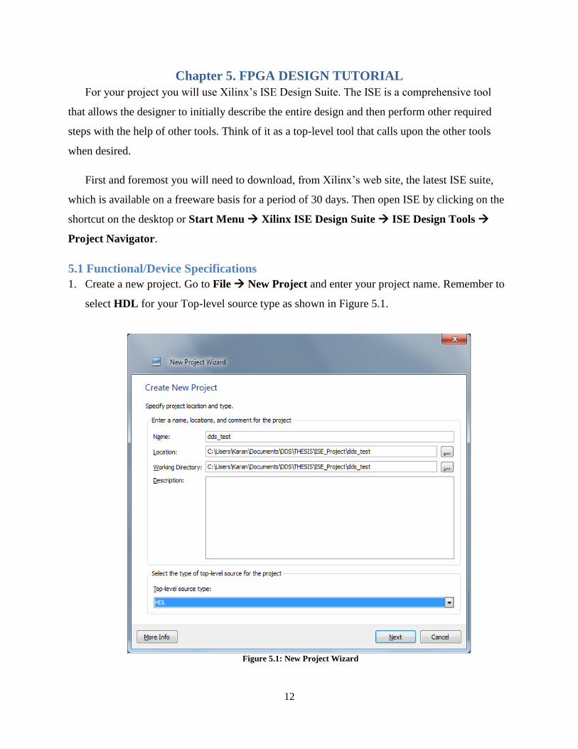
1. Create a new project. Go to File New Project and enter your project name. Remember to
select HDL for your Top-level source type as shown in Figure 5.1.
Figure 5.1: New Project Wizard
13
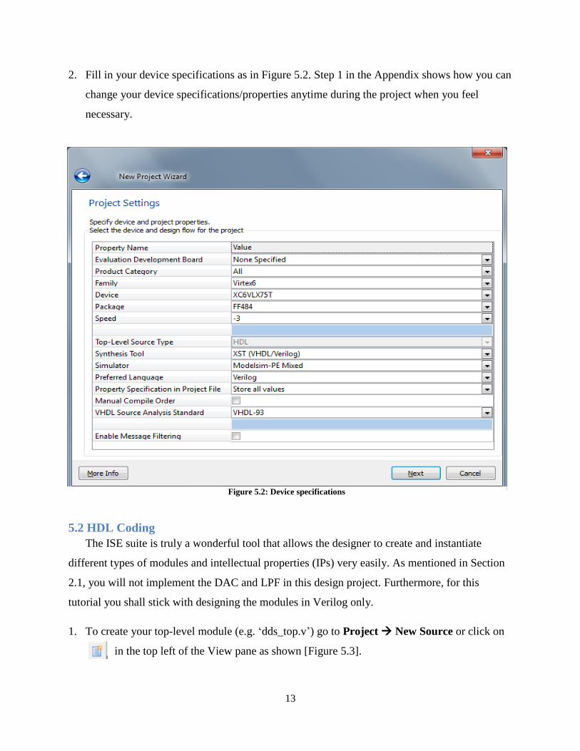
2. Fill in your device specifications as in Figure 5.2. Step 1 in the Appendix shows how you can
change your device specifications/properties anytime during the project when you feel
necessary.
5.2 HDL Coding
The ISE suite is truly a wonderful tool that allows the designer to create and instantiate
different types of modules and intellectual properties (IPs) very easily. As mentioned in Section
2.1, you will not implement the DAC and LPF in this design project. Furthermore, for this
tutorial you shall stick with designing the modules in Verilog only.
1. To create your top-level module (e.g. ‘dds_top.v’) go to Project New Source or click on
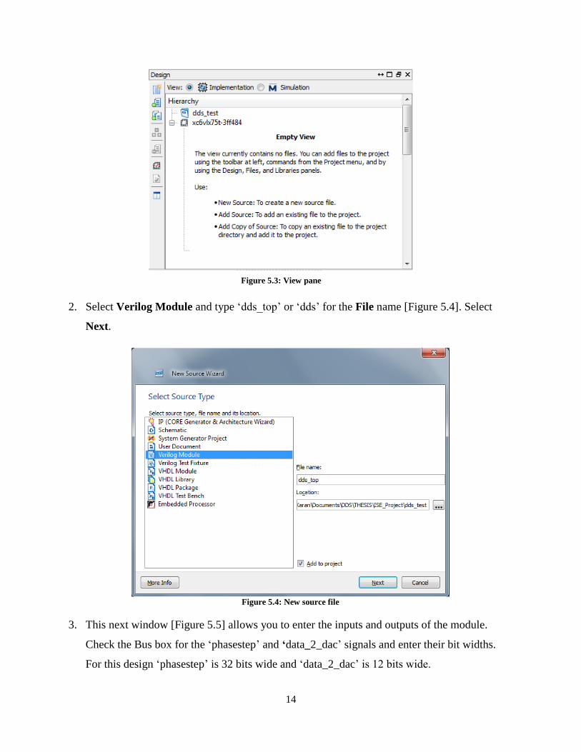
in the top left of the View pane as shown [Figure 5.3].
Figure 5.2: Device specifications
14
2. Select Verilog Module and type ‘dds_top’ or ‘dds’ for the File name [Figure 5.4]. Select
Next.
3. This next window [Figure 5.5] allows you to enter the inputs and outputs of the module.
Check the Bus box for the ‘phasestep’ and ‘data_2_dac’ signals and enter their bit widths.
For this design ‘phasestep’ is 32 bits wide and ‘data_2_dac’ is 12 bits wide.
Figure 5.3: View pane
Figure 5.4: New source file

15
4. Once you go ahead, you will get a Verilog file as shown below on the left side of Figure 5.6.
Figure 5.5: Configuring inputs and outputs
Figure 5.6: Stating inputs and outputs in a module

16
Figure 5.6 also indicates how to start any Verilog file. Verilog allows you the flexibility to
assign port calling slightly differently, by first defining the names of the inputs and outputs
and then later categorizing them. The alternative representation is shown on the right hand
side of the Figure 5.6.
5. An extremely nice feature of ISE is that Xilinx has given the designers access to many
templates that are readily available in the tool. For example, if you need to make a function
declaration or create a flip-flop, lookup table, comparator, encoder, decoder, or user
constraint file (UCF), etc., go to Edit Language Templates Verilog/UCF and select
the appropriate device. To instantiate the same in your design file, right-click on the desired
template and select Use in File [Figure 5.7].
Figure 5.7: Instantiating examples of code

17
6. The ISE tool allows you to easily implement Xilinx IPs. When using IPs it is important to
select the right family and device of the FPGA (Section 5.1, step 2) since the devices you
implement are completely dependent on the type of FPGA used.
For this DDS you will be using two such IPs. In the top-level DDS file (‘dds_top.v’ or
‘dds.v’) you will implement the Phase Accumulator, and then later on you will implement a
Block Memory Generator for the sine LUT.
To generate the phase accumulator IP, go to Project New Source (as seen before in
Section 5.1, step 1) and type ‘Accumulator’ for the File Name. Select IP (CORE Generator
& Architecture Wizard for the source type [Figure 5.8].
7. Once you go to the next page, notice that you can select your IP according to its function or
view it by its name. Select Basic Elements Accumulators and add the Accumulator IP.
A window as shown in Figure 5.9 should open.
Figure 5.8: Generating an IP

18
8. For this DDS design you will use a 32 bit input and output PAC. So, for the next stage,
change the following variables to the values shown below:
a. Input Type: Unsigned
b. Input Width: 32
c. Output Width: 32
d. Latency Configuration: Automatic
e. Bypass: Unchecked
9. Leave everything else unchanged and click Generate. Figure 5.10 should now show what
your View pane should look like.
Figure 5.9: Accumulator IP
Figure 5.10: View pane showing Accumulator not instantiated

19
10. Figure 5.10 shows that the Accumulator has been generated but not been instantiated within
the design. ISE has a very unique feature that shows you how to instantiate any module that
you generate or create. To do the following select the Accumulator IP and double-click on
View HDL Instantiation Template in the Processes pane (located below the View pane).
Copy the relevant code, paste it within the top-level entity and edit the inputs and outputs of
the module. Your top-level entity will now contain an instantiation of the module as marked
within Figure 5.11.
11. The next IP that you need to embed is the sine Lookup Table. For this IP, instantiate the
Block Memory Generator and make the following changes, while leaving everything else
the same:
a. Interface type: Native. Go to the Next page
b. Memory Type: Single Port ROM
c. Algorithm: Low Power. Go to the Next page
d. Read Width: 12
e. Read Depth: 4096. Go to the Next page
f. Register Port A Output of Memory Primitives: Checked
g. Register Port A Output of Memory Core: Checked
h. Pipeline Stages within Mux: 3
i. Load Init File: Checked
Figure 5.11: Instantiating an IP
20
j. Select the file with the sine wave coefficients you generated in Section 2.1. Go to the
Next page and eventually Generate the module
12. When you instantiate the LUT in the design, make sure to implement a conversion algorithm
that changes the output of the ROM depending on the two highest most significant bits
(MSBs). This algorithm is necessary to create an entire sine wave period from only a quarter
sine wave period that you stored. Now you can go ahead and design the remaining
components.
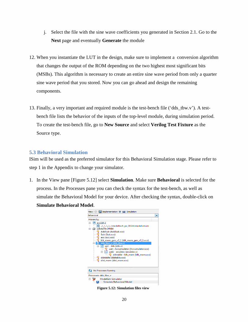
13. Finally, a very important and required module is the test-bench file (‘dds_tbw.v’). A test-
bench file lists the behavior of the inputs of the top-level module, during simulation period.
To create the test-bench file, go to New Source and select Verilog Test Fixture as the
Source type.
5.3 Behavioral Simulation
ISim will be used as the preferred simulator for this Behavioral Simulation stage. Please refer to
step 1 in the Appendix to change your simulator.
1. In the View pane [Figure 5.12] select Simulation. Make sure Behavioral is selected for the
process. In the Processes pane you can check the syntax for the test-bench, as well as
simulate the Behavioral Model for your device. After checking the syntax, double-click on
Simulate Behavioral Model.
Figure 5.12: Simulation files view
21
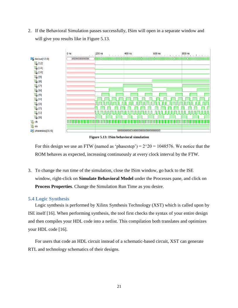
2. If the Behavioral Simulation passes successfully, ISim will open in a separate window and
will give you results like in Figure 5.13.
For this design we use an FTW (named as ‘phasestep’) = 2^20 = 1048576. We notice that the
ROM behaves as expected, increasing continuously at every clock interval by the FTW.
3. To change the run time of the simulation, close the ISim window, go back to the ISE
window, right-click on Simulate Behavioral Model under the Processes pane, and click on
Process Properties. Change the Simulation Run Time as you desire.
5.4 Logic Synthesis
Logic synthesis is performed by Xilinx Synthesis Technology (XST) which is called upon by
ISE itself [16]. When performing synthesis, the tool first checks the syntax of your entire design
and then compiles your HDL code into a netlist. This compilation both translates and optimizes
your HDL code [16].
For users that code an HDL circuit instead of a schematic-based circuit, XST can generate
RTL and technology schematics of their designs.
Figure 5.13: ISim behavioral simulation

22
1. The first step to synthesize your circuit is to set up the properties of the process. Right-click
on Synthesize and click on Process Properties. Adjust the Property display level to
Advanced. Go to the Synthesis Options tab and set Netlist Hierarchy to Rebuilt as in Figure
5.14. Click OK.
2. Double-click on Synthesize-XST in the Processes pane.
3. Expand the Synthesize-XST tab in the Processes pane. To view the generated RTL
schematic, double-click on the same. Select Start with the Explorer Wizard and click OK.
Select the top-level module and Add it to the Selected Elements and then click on Create
Schematic [Figure 5.15].
Figure 5.14: Process Properties – Synthesis Options
Figure 5.15: Creating an RTL schematic
23
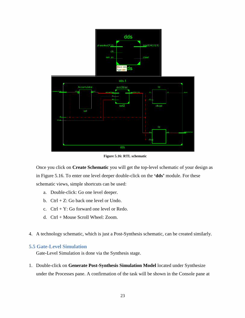
Once you click on Create Schematic you will get the top-level schematic of your design as
in Figure 5.16. To enter one level deeper double-click on the ‘dds’ module. For these
schematic views, simple shortcuts can be used:
a. Double-click: Go one level deeper.
b. Ctrl + Z: Go back one level or Undo.
c. Ctrl + Y: Go forward one level or Redo.
d. Ctrl + Mouse Scroll Wheel: Zoom.
4. A technology schematic, which is just a Post-Synthesis schematic, can be created similarly.
5.5 Gate-Level Simulation
Gate-Level Simulation is done via the Synthesis stage.
1. Double-click on Generate Post-Synthesis Simulation Model located under Synthesize
under the Processes pane. A confirmation of the task will be shown in the Console pane at
Figure 5.16: RTL schematic

24
the bottom of the window. When the model gets generated, open the Design Summary tab.
If you cannot find the tab go to Project Design Summary/Reports.
2. To view the Synthesis report, in the main window, double-click on Synthesis Report under
Detailed Reports [Figure 5.17]. From this report the designer can view vital information like
the design summary incorporating the final registers/flip-flops count, total number of gates
used, clock information, and different critical paths and their timings.
5.6 Mapping, Placement and Route (PAR)
The entire process of Mapping and PAR falls under the design implementation block. Design
implementation also incorporates another additional step in the beginning called Translate.
According to Reference [14] this process “combines all the input netlists and (user) constraints to
a logic design file. This information is saved as a Native Generic Database (NGD).” Once the
Figure 5.17: Synthesis timing report

25
Translate process has been completed the embedded tool automatically performs the Mapping
and PAR.
1. As a prerequisite to implementing any design on an FPGA, a user constraint file (UCF) is
required which will first need to be created. To do so, click on New Source, select
Implementation Constraints File, type the file name and click Next.
2. In the View pane, select the top-level entity, and in the Processes pane expand User
Constraints, and double-click on Create Timing Constraints. You will get a window
similar to the one shown in Figure 5.18.
Double-click on the clk signal in the Unconstrained Clocks section and enter ‘2.1 ns’ in the
Specify time category within the Clock signal definition. Let the default Duty cycle of 50%
be unchanged. Note: we use a 2.1 ns period because we use a 475 MHz clock frequency.
In the Constraint Type window (on the left) go to Inputs and double-click on clk in the Is
Constrained by a Global OFFSET IN field. In the new window set the desired clock type and
click Next. Enter in the desired external setup time and data valid duration. In this tutorial 2.1
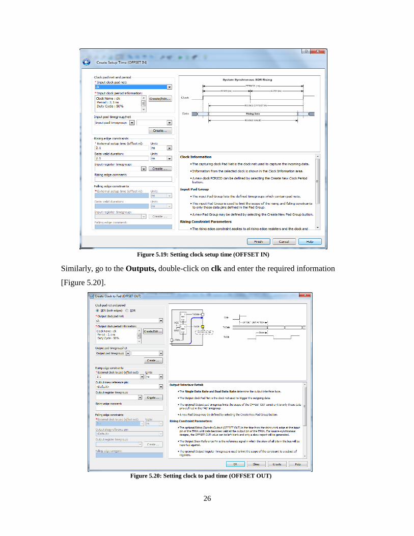
ns has been chosen for both [Figure 5.19].
Figure 5.18: Setting clock constraints
26
Similarly, go to the Outputs, double-click on clk and enter the required information
[Figure 5.20].
Figure 5.19: Setting clock setup time (OFFSET IN)
Figure 5.20: Setting clock to pad time (OFFSET OUT)
27
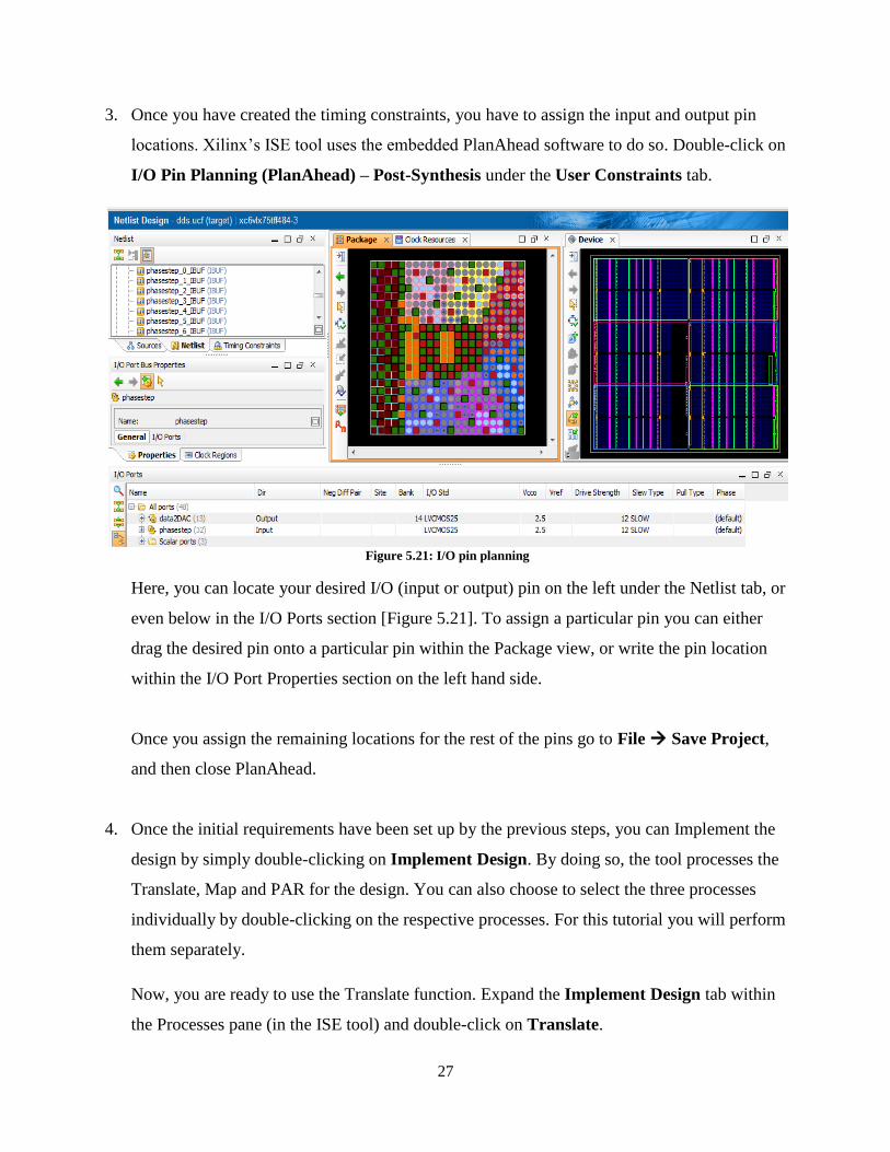
3. Once you have created the timing constraints, you have to assign the input and output pin
locations. Xilinx’s ISE tool uses the embedded PlanAhead software to do so. Double-click on
I/O Pin Planning (PlanAhead) – Post-Synthesis under the User Constraints tab.
Here, you can locate your desired I/O (input or output) pin on the left under the Netlist tab, or
even below in the I/O Ports section [Figure 5.21]. To assign a particular pin you can either
drag the desired pin onto a particular pin within the Package view, or write the pin location
within the I/O Port Properties section on the left hand side.
Once you assign the remaining locations for the rest of the pins go to File Save Project,
and then close PlanAhead.
4. Once the initial requirements have been set up by the previous steps, you can Implement the
design by simply double-clicking on Implement Design. By doing so, the tool processes the
Translate, Map and PAR for the design. You can also choose to select the three processes
individually by double-clicking on the respective processes. For this tutorial you will perform
them separately.
Now, you are ready to use the Translate function. Expand the Implement Design tab within
the Processes pane (in the ISE tool) and double-click on Translate.
Figure 5.21: I/O pin planning
28
5. To Map the design, expand the Implement Design tab within the Processes pane and double-
click on Map.
6. When the Mapping has been completed double-click on Generate Post-Map Simulation
Model and open the Design Summary tab to view the Map Report.
To view the static timing analysis of the circuit after the Mapping stage, double-click on
Generate Post-Map Static Timing, expand the same and double-click on Analyze Post-
Map Static Timing.
When the report opens up we notice that the STA gives us an upper bound of the clock
frequency. Initially, the clock period was set to 2.1 ns (475 MHz), but the Post-Map result
shows that now a 541 MHz clock (1.847 ns period) can be achieved for the design.
7. To place and route the design, expand the Implement Design tab within the Processes pane
and double-click on Place & Route.
5.7 Static Timing Analysis (STA)
To view the STA of the circuit after the PAR, double-click on Generate Post-Place &
Route Static Timing, then expand the same and double-click on Analyze Post- Place & Route
Static Timing.
When the report opens up you will notice that the STA will give you a new upper bound
clock frequency. Here, you initially set a 2.1 ns clock period (475 MHz), but the Post-PAR result
shows that you can achieve a 556 MHz source clock (1.798 ns period) for the design. Note, the
Post-Map STA gave a max clock frequency of 541 MHz clock (1.847 ns period).
5.8 Post PAR Timing Simulation
Once the PAR has been completed, double-click on Generate Post-Map Simulation Model
and open the Design Summary tab to view the PAR report.
5.9 FPGA Configuration and Programming
To program the FPGA and generate a bitstream file, ISE will use its embedded tool
iMPACT.

29
1. Select the top-level entity and right-click on Generate Programming File located under the
Processes pane. Now click on Process Properties. Select Startup Options in the Category
list, and make sure that the FPGA Start-Up clock is selected to CCLK. For devices that are
configured from the PROM of the development board, it is suggested to use the CCLK
option [1]. Click OK.
Double-click on Generate Programming File. This will create a bitstream file named
‘dds.bit’. This file will later be used to put onto the FPGA.
2. The next step in the process is to create a PROM (Programmable Read Only Memory) file
that will be used to program the FPGA. As page 119 of Reference [16] states, “In the
Processes pane, expand Configure Target Device, and double-click Generate Target
PROM/ACE File.”
Once iMPACT opens [Figure 5.22], double-click on Create PROM File and a PROM File
Formatter window will open up as in Figure 5.23.
Figure 5.22: iMPACT
Figure 5.23: Generating a bitstream file for the PROM

30
As shown in Figure 5.23, select Xilinx Flash/PROM, press the Green arrow button, then
Check the Auto Select PROM option and press the next Green arrow button. Enter your
desired output file name, and press OK. In the new window, add your ‘bit’ file. Select No
when it asks you to add another file. A window like Figure 5.24 should now open.
Select the Xilinx FPGA icon on the right, and then double-click on Generate File in the
iMPACT Processes pane on the left side [Figure 5.25].
3. Save the iMPACT project. This project file can be imported later directly onto the FPGA
whenever required.
Figure 5.24: iMPACT generate file process
Figure 5.25: Bit file generation

31
5.10 Final Behavioral Simulations
You will use ModelSim to view the Post-Map simulated behavior of the design because
ModelSim has a unique feature of viewing any signal as an analog waveform. Since the FPGA
does not have a DAC onboard, this feature is extremely useful to view the final output as a
proper sine wave. Please refer to the Appendix to set up ModelSim as the simulator.
1. Once you set up ModelSim, select Simulation under the view pane and change the process to
Post-Map. Select the project file in the View pane and in the Processes pane double-click on
Compile HDL Simulation Libraries [Figure 5.26]. This command will compile all the
necessary libraries required by ModelSim. Note, this process will take a long time
(approximately less than 1.5 hours).
Once the compilation process has been completed, select the top-level entity’s test-bench file
and double-click on Simulate Behavioral Model [Figure 5.27].
Figure 5.26: Compilation of libraries
Figure 5.27: Ready to simulate Post-Map model
32
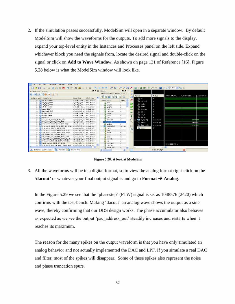
2. If the simulation passes successfully, ModelSim will open in a separate window. By default
ModelSim will show the waveforms for the outputs. To add more signals to the display,
expand your top-level entity in the Instances and Processes panel on the left side. Expand
whichever block you need the signals from, locate the desired signal and double-click on the
signal or click on Add to Wave Window. As shown on page 131 of Reference [16], Figure
5.28 below is what the ModelSim window will look like.
3. All the waveforms will be in a digital format, so to view the analog format right-click on the
‘dacout’ or whatever your final output signal is and go to Format Analog.
In the Figure 5.29 we see that the ‘phasestep’ (FTW) signal is set as 1048576 (2^20) which
confirms with the test-bench. Making ‘dacout’ an analog wave shows the output as a sine
wave, thereby confirming that our DDS design works. The phase accumulator also behaves
as expected as we see the output ‘pac_address_out’ steadily increases and restarts when it
reaches its maximum.
The reason for the many spikes on the output waveform is that you have only simulated an
analog behavior and not actually implemented the DAC and LPF. If you simulate a real DAC
and filter, most of the spikes will disappear. Some of these spikes also represent the noise
and phase truncation spurs.
Figure 5.28: A look at ModelSim

33
4. To change the frequency of the sine wave, go back to ISE edit the FTW in the test-bench file,
and re-run the simulation (no need to re-compile the libraries).
5. To view the expected behavior after PAR, change the simulation type to Post-Route and
repeat the above steps.
Figure 5.29: ModelSim's Post-Map simulated output

34
Chapter 6. DDS MEASUREMENTS
This chapter discusses the final timing results and different simulation wave forms that were
achieved with the DDS design for the FPGA.
6.1 Timing Reports
When designing any circuit for an FPGA, the different processes involved will continuously
try and optimize the code, thereby making it more efficient. Table 6.1 shows one such example
that was achieved with the maximum attainable source clock frequency.
From the above table we can see that, as the design progressed through the different stages,
we got a much faster source clock than what was initially set up.
6.2 Behavioral and Post Map Simulations
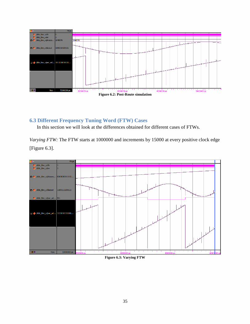
Figures 6.1 and 6.2 show the final waveforms from the behavioral simulation and the Post-
PAR simulation, respectively, with the FTW set at 1048576. On comparison of the two figures,
you will notice that the Post-Route waveform has many spikes. These spikes are due to the phase
truncation spurs. Implementing the DAC and LPF should dramatically reduce these spurs.
Table 6.1 Clock frequency at different stages
Clock Initial Setup Post Synthesis Post Map Post PAR
Maximum
Frequency 476.19 MHz 558.972 MHz 541.419 MHz 556.174 MHz
Minimum Time
Period 2.1 ns 1.789 ns 1.847 ns 1.798 ns
Figure 6.1: Behavioral simulation
35
6.3 Different Frequency Tuning Word (FTW) Cases
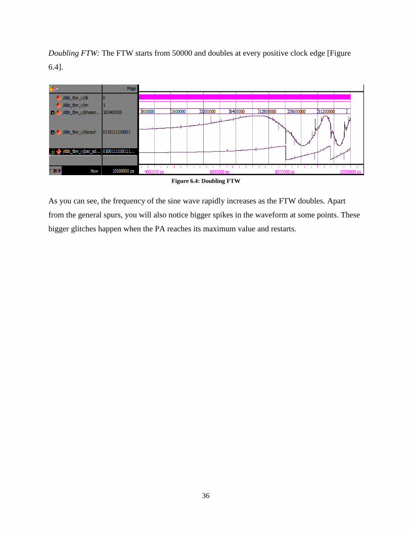
In this section we will look at the differences obtained for different cases of FTWs.
Varying FTW: The FTW starts at 1000000 and increments by 15000 at every positive clock edge
[Figure 6.3].
Figure 6.2: Post-Route simulation
Figure 6.3: Varying FTW
36
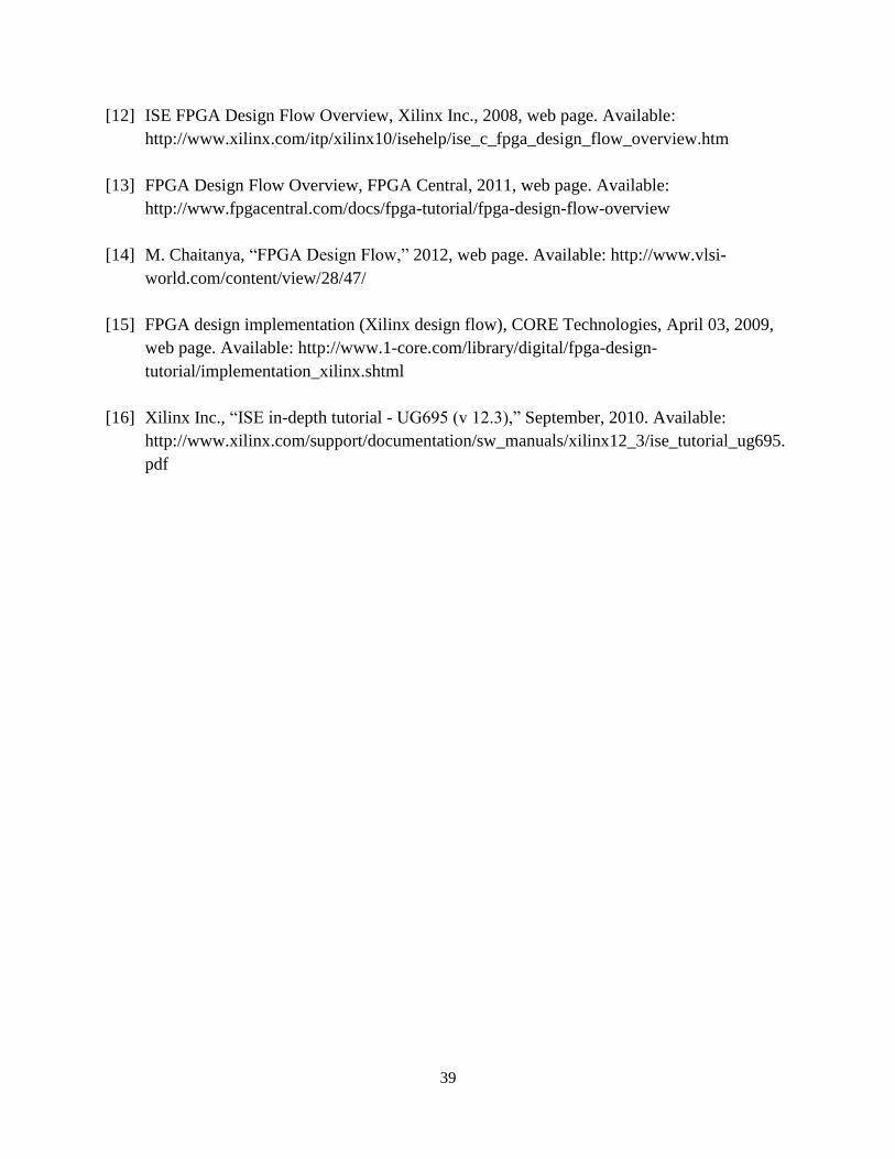
Doubling FTW: The FTW starts from 50000 and doubles at every positive clock edge [Figure
6.4].
As you can see, the frequency of the sine wave rapidly increases as the FTW doubles. Apart
from the general spurs, you will also notice bigger spikes in the waveform at some points. These
bigger glitches happen when the PA reaches its maximum value and restarts.
Figure 6.4: Doubling FTW

37
Chapter 7. CONCLUSION AND FUTURE WORK
In summary, this thesis laid down the path necessary to gain knowledge to design any circuit
for an FPGA, using a DDS as an example. It started by stating some Verilog examples that are
used for the HDL to design digital circuits and then went on to explain the background theory of
a DDS. This was followed by a broad overview on the essentials of FPGA design. These three
chapters are a stepping stone to any FPGA design. Using Xilinx’s ISE software and
implementing the DDS on a Virtex 6 FPGA, the tutorial stepped through the different phases of
an FPGA flow diagram and simultaneously showed screenshots to help orient the user. Finally,
the thesis investigated the different results which were obtained when the inputs were varied.
This project does not implement an actual DAC, thus the next step would be to implement
the DDS on the FPGA and feed the signal to a DAC and LPF whose output would then be given
to an oscilloscope. There are also many algorithms being developed in the industry to reduce the
different spurs generated in the DDS. Thus, additional future work for this project could entail
implementing some of those algorithms in the design, and comparing a generic to an optimized
DDS.

38
References
[1] Analog Devices, “A technical tutorial on digital signal synthesis,” Application Note, 1999.
Available: http://www.analog.com/static/imported-
files/tutorials/450968421DDS_Tutorial_rev12-2-99.pdf
[2] T. M. Comberiate, “Phase noise spur reduction in an array of direct digital synthesizers,”
M.S. thesis, University of Illinois at Urbana-Champaign, Urbana, IL, 2010.
[3] C. Shan, Z. Chen, H. Yuan and W. Hu, “Design and implementation of a FPGA-based
direct digital synthesizer,” in Electrical and Control Engineering (ICECE), 2011
International Conference, pp.614-617.
[4] H. Omran, K. Sharaf, and M. Ibrahim, “An all-digital direct digital synthesizer fully
implemented on FPGA,” in Design and Test Workshop (IDT), 2009 4th International,
pp.1-6.
[5] C. E. Shannon, “Communication in the presence of noise,” Proceedings of the IRE, January
1949, vol. 37, no. 1, pp. 10- 21.
[6] J. Vankka, Digital Synthesizers and Transmitters for Software Radio. Dordrecht, The
Netherlands: Springer, 2005.
[7] Y. Yang, “A novel truncation spurs free structure of direct digital synthesizer,” 2011,
unpublished.
[8] World of ASIC, 2012, web site. Available: http://www.asic-world.com/
[9] D. K. Tala, “Verilog Tutorial,” 2012, Available:
http://www.ece.umd.edu/courses/enee359a/verilog_tutorial.pdf
[10] FPGA vs. ASIC, Xilinx Inc., 2012, web page. Available:
http://www.xilinx.com/fpga/asic.htm
[11] B. Mullane and C. MacNamee, “Developing a reusable IP platform within a system-on-
chip design framework targeted towards an academic R&D environment,” Circuits and
System Research Centre (CSRC), University of Limerick, Limerick, Ireland, web page.
Available: http://www.design-reuse.com/articles/16039/developing-a-reusable-ip-platform-
within-a-system-on-chip-design-framework-targeted-towards-an-academic-r-d-
environment.html
39
[12] ISE FPGA Design Flow Overview, Xilinx Inc., 2008, web page. Available:
http://www.xilinx.com/itp/xilinx10/isehelp/ise_c_fpga_design_flow_overview.htm
[13] FPGA Design Flow Overview, FPGA Central, 2011, web page. Available:
http://www.fpgacentral.com/docs/fpga-tutorial/fpga-design-flow-overview
[14] M. Chaitanya, “FPGA Design Flow,” 2012, web page. Available: http://www.vlsi-
world.com/content/view/28/47/
[15] FPGA design implementation (Xilinx design flow), CORE Technologies, April 03, 2009,
web page. Available: http://www.1-core.com/library/digital/fpga-design-
tutorial/implementation_xilinx.shtml
[16] Xilinx Inc., “ISE in-depth tutorial - UG695 (v 12.3),” September, 2010. Available:
http://www.xilinx.com/support/documentation/sw_manuals/xilinx12_3/ise_tutorial_ug695.

40
Appendix. CHOOSING A SIMULATOR AND
SETTING UP MODELSIM
1. To choose either ISim or ModelSim as your simulator, right-click on your top-level entity
and select Design Properties [Figure A.1].
Now choose your desired simulator in the Simulator drop-down field. In Figure A.2,
‘Modelsim-PE Mixed’ has been chosen. For ISim, select the same from the drop-down menu.
Figure A.1: Selecting design properties
Figure A.2: Design properties

41
2. Once you have ModelSim downloaded and installed, go back to ISE, go to Edit
Preferences, expand ISE General, and select Integrated Tools. Add the path to the
ModelSim executable file in the Model Tech Simulator section and click OK [Figure A.3].
Now you have to add the ‘modelsim.ini’ file to your project. Go to Project Add Source.
In the bottom-right change the view option to All files, then browse to the ModelSim
directory and add the ‘modelsim.ini’ file. Generally it will be in C:\modeltech_pe_10.1b
[Figure A.4].
Figure A.3: Giving the path to ModelSim
Figure A.4: Selecting the 'modelsim.ini' file