© 2000 prentice hall inc. figure 6.1 and operation
TRANSCRIPT
© 2000 Prentice Hall Inc.
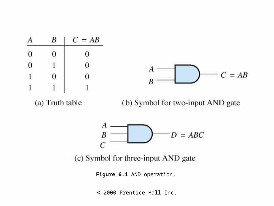
Figure 6.1 AND operation.

© 2000 Prentice Hall Inc.
Figure 6.2 NOT operation.

© 2000 Prentice Hall Inc.
Figure 6.3 OR operation.

© 2000 Prentice Hall Inc.
Figure 6.4 Additional logic-gate symbols.
© 2000 Prentice Hall Inc.
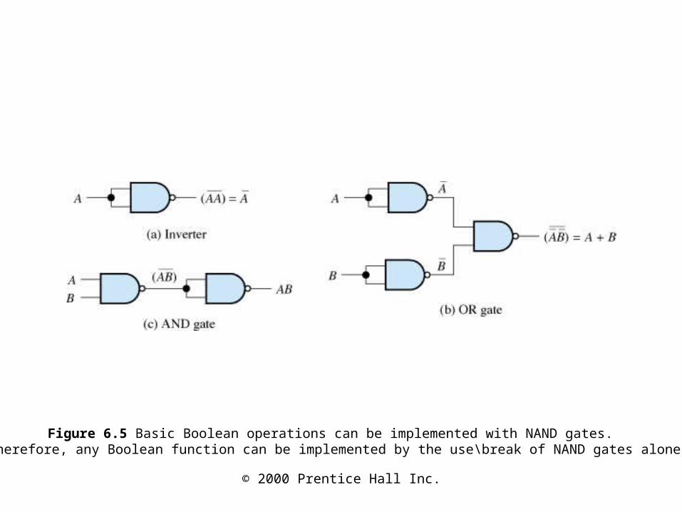
Figure 6.5 Basic Boolean operations can be implemented with NAND gates. Therefore, any Boolean function can be implemented by the use\break of NAND gates alone.

© 2000 Prentice Hall Inc.
Figure 6.6 The AND, OR, and\break NOT operations can be implemented with NOR gates. See Exercise 6.1.
© 2000 Prentice Hall Inc.
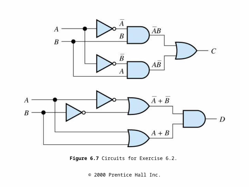
Figure 6.7 Circuits for Exercise 6.2.

© 2000 Prentice Hall Inc.
Figure 6.8 Output voltage ranges for the 7400 ALS TTL logic family.

© 2000 Prentice Hall Inc.
Figure 6.9 Logic inverter.
© 2000 Prentice Hall Inc.
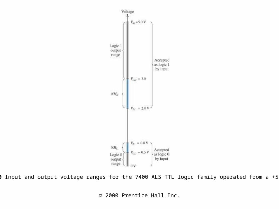
Figure 6.10 Input and output voltage ranges for the 7400 ALS TTL logic family operated from a +5-V supply.

© 2000 Prentice Hall Inc.
Figure 6.11 Reference directions for input and output currents. (I_O has a negative value if the output sources current.)
© 2000 Prentice Hall Inc.
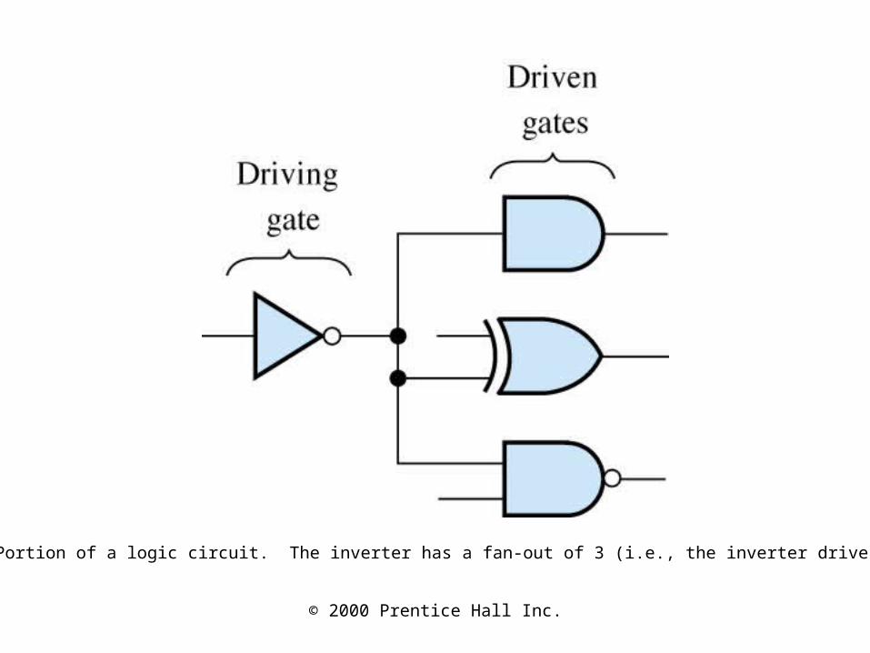
Figure 6.12 Portion of a logic circuit. The inverter has a fan-out of 3 (i.e., the inverter drives 3 inputs).
© 2000 Prentice Hall Inc.
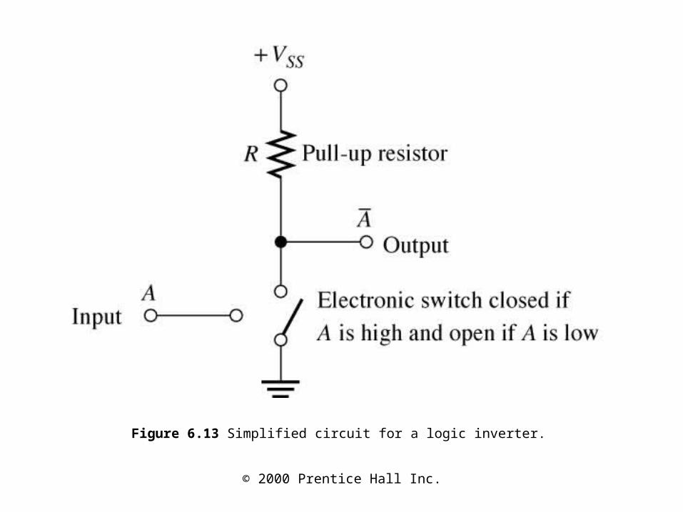
Figure 6.13 Simplified circuit for a logic inverter.

© 2000 Prentice Hall Inc.
Figure 6.14 Load capacitance causes dynamic power dissipation in a logic gate.

© 2000 Prentice Hall Inc.
Figure 6.15 Input pulse and output of a typical inverter.
© 2000 Prentice Hall Inc.
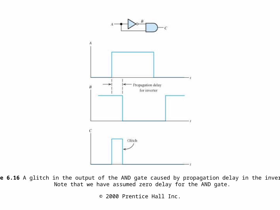
Figure 6.16 A glitch in the output of the AND gate caused by propagation delay in the inverter. Note that we have assumed zero delay for the AND gate.
© 2000 Prentice Hall Inc.
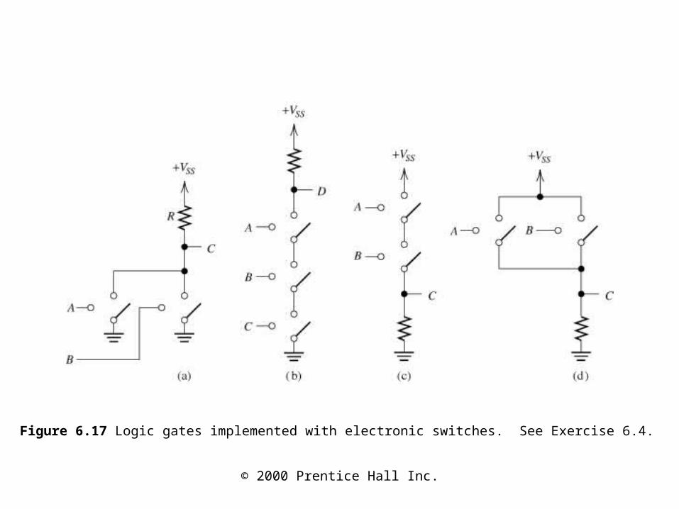
Figure 6.17 Logic gates implemented with electronic switches. See Exercise 6.4.

© 2000 Prentice Hall Inc.
Figure 6.18 MOS inverter with pull-up resistor.

© 2000 Prentice Hall Inc.
Figure 6.19 Load-line analysis for the circuit of Figure 6.18a.
© 2000 Prentice Hall Inc.
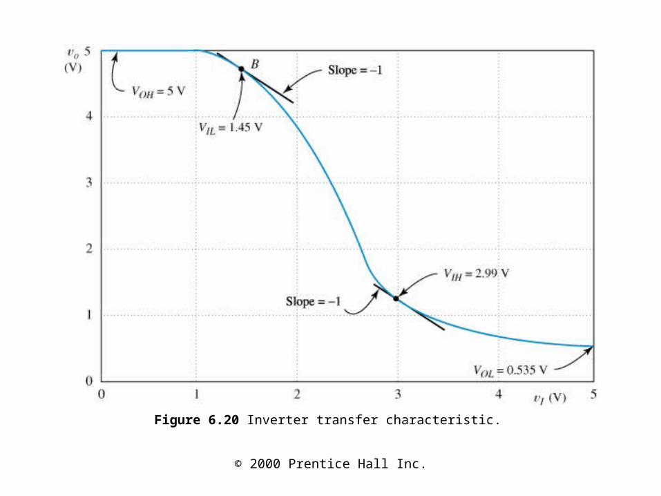
Figure 6.20 Inverter transfer characteristic.

© 2000 Prentice Hall Inc.
Figure 6.21a & b The low-to-high output transition of the resistor pull-up NMOS inverter.
© 2000 Prentice Hall Inc.
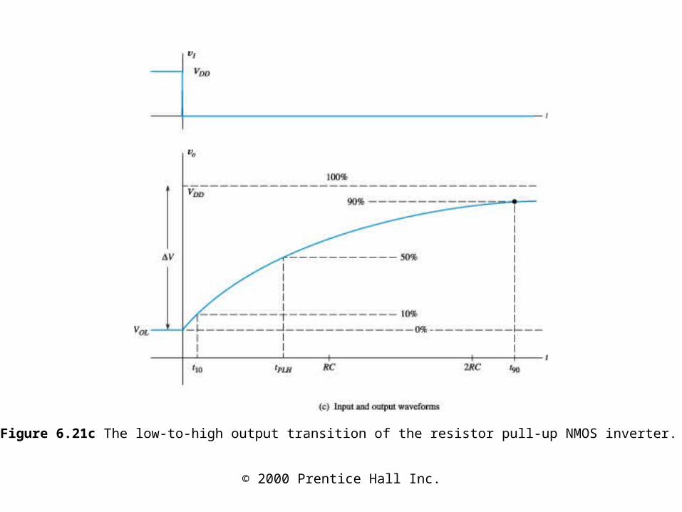
Figure 6.21c The low-to-high output transition of the resistor pull-up NMOS inverter.
© 2000 Prentice Hall Inc.
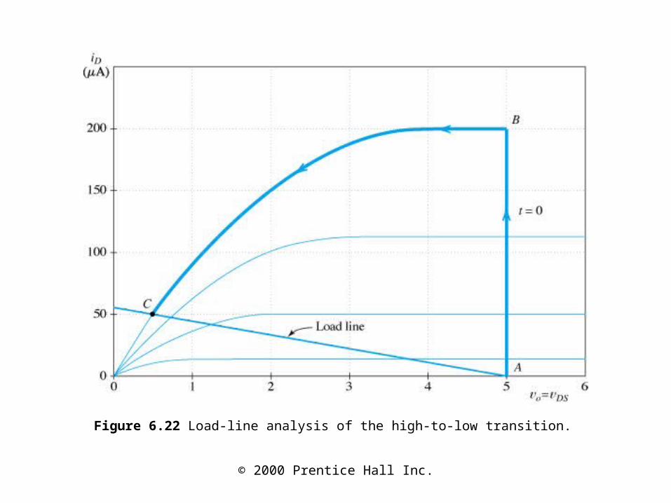
Figure 6.22 Load-line analysis of the high-to-low transition.

© 2000 Prentice Hall Inc.
Figure 6.23 Cascade of three inverters.
© 2000 Prentice Hall Inc.
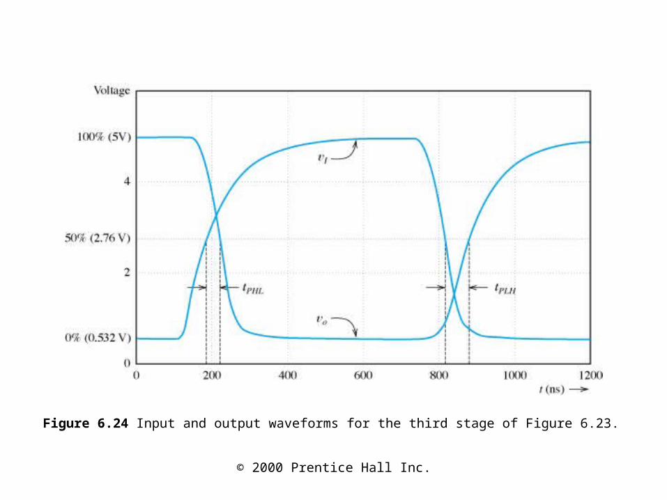
Figure 6.24 Input and output waveforms for the third stage of Figure 6.23.
© 2000 Prentice Hall Inc.
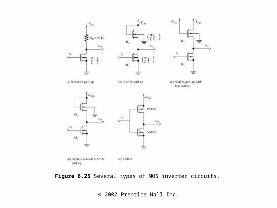
Figure 6.25 Several types of MOS inverter circuits.

© 2000 Prentice Hall Inc.
Figure 6.26 Circuit for Example 6.6.

© 2000 Prentice Hall Inc.
Figure 6.29 Transfer characteristic of the NMOS pull-up inverter.
© 2000 Prentice Hall Inc.
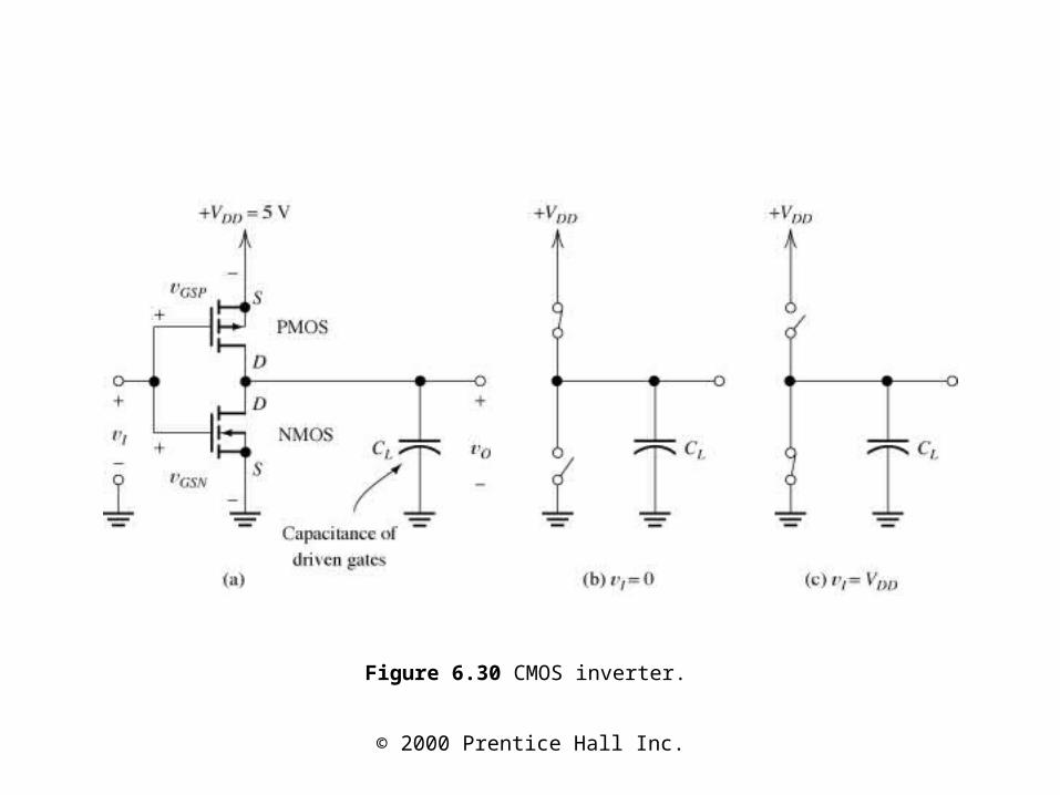
Figure 6.30 CMOS inverter.
© 2000 Prentice Hall Inc.
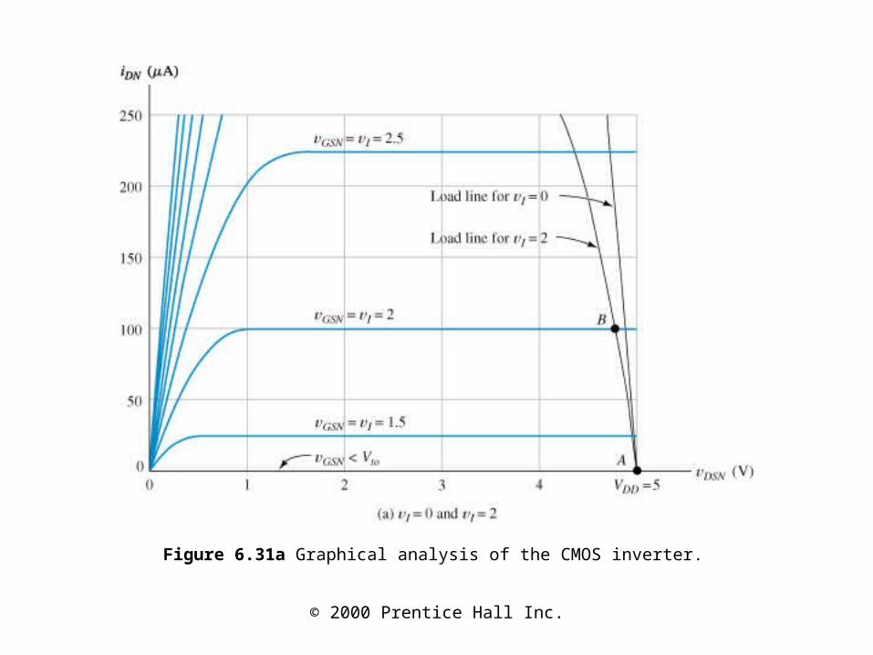
Figure 6.31a Graphical analysis of the CMOS inverter.

© 2000 Prentice Hall Inc.
Figure 6.31b Graphical analysis of the CMOS inverter.

© 2000 Prentice Hall Inc.
Figure 6.32 Transfer characteristic of a typical CMOS inverter. The lettered points correspond to the points of Figure 6.31.

© 2000 Prentice Hall Inc.
Figure 6.33 Supply current for a CMOS inverter.
© 2000 Prentice Hall Inc.
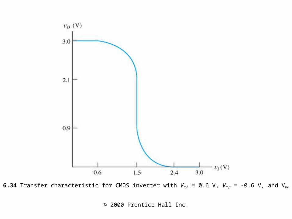
Figure 6.34 Transfer characteristic for CMOS inverter with Vton = 0.6 V, Vtop = -0.6 V, and VDD = 3V.

© 2000 Prentice Hall Inc.
Figure 6.35 The high-to-low transition of the CMOS inverter.
© 2000 Prentice Hall Inc.
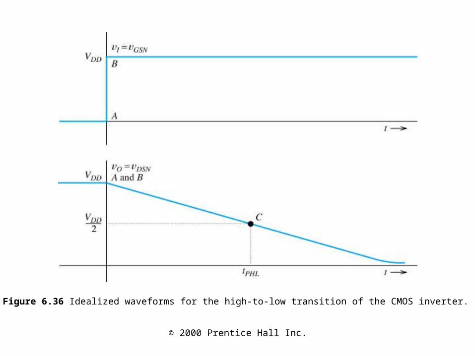
Figure 6.36 Idealized waveforms for the high-to-low transition of the CMOS inverter.

© 2000 Prentice Hall Inc.
Figure 6.37 Cascade of three CMOS inverters.

© 2000 Prentice Hall Inc.
Figure 6.38 Waveforms for stage three of Figure 6.37.
© 2000 Prentice Hall Inc.
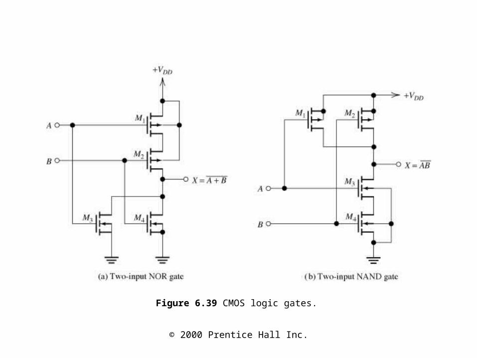
Figure 6.39 CMOS logic gates.

© 2000 Prentice Hall Inc.
Figure 6.40 Three-input NOR gate.

© 2000 Prentice Hall Inc.
Figure 6.41 Circuits used to plot the transfer characteristics of a two-input NAND gate.

© 2000 Prentice Hall Inc.
Figure 6.45 Transfer characteristics of a two-input NAND gate.
© 2000 Prentice Hall Inc.
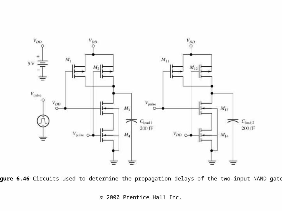
Figure 6.46 Circuits used to determine the propagation delays of the two-input NAND gate.

© 2000 Prentice Hall Inc.
Figure 6.47 Switching transients of the two-input NAND gate.

© 2000 Prentice Hall Inc.
Figure 6.48 Static CMOS gates contain redundant switching functions.

© 2000 Prentice Hall Inc.
Figure 6.49 Dynamic logic NOR gate.
© 2000 Prentice Hall Inc.
Figure 6.50 Dynamic CMOS implementation of F= (AB+C+DE).

© 2000 Prentice Hall Inc.
Figure 6.51 CMOS analog switch.

© 2000 Prentice Hall Inc.
Figure 6.52 Equivalent circuit and symbol for the CMOS transmission gate.

© 2000 Prentice Hall Inc.
Figure 6.53 Pass transistor logic.