zynq-7000 all programmable soc architecture porting quick start
TRANSCRIPT
Zynq-7000 All Programmable SoC Architecture Porting Quick Start Guide
UG1181 (v1.1.1) October 22, 2015
Architecture Porting Guide www.xilinx.com 2UG1181 (v1.1.1) October 22, 2015
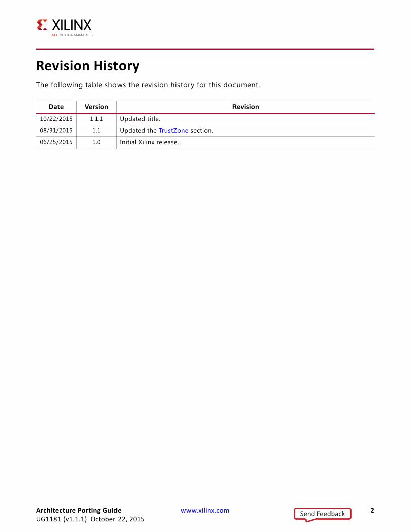
Revision HistoryThe following table shows the revision history for this document.
Date Version Revision
10/22/2015 1.1.1 Updated title.
08/31/2015 1.1 Updated the TrustZone section.
06/25/2015 1.0 Initial Xilinx release.
Send Feedback

Architecture Porting Guide www.xilinx.com 3UG1181 (v1.1.1) October 22, 2015
Table of ContentsRevision History . . . . . . . . . . . . . . . . . . . . . . . . . . . . . . . . . . . . . . . . . . . . . . . . . . . . . . . . . . . . . . . . . . . . 2
Chapter 1: Introduction
Chapter 2: Porting ConsiderationsARM Cortex-A9 Features . . . . . . . . . . . . . . . . . . . . . . . . . . . . . . . . . . . . . . . . . . . . . . . . . . . . . . . . . . . . 6
Chapter 3: Feature Comparison Across ArchitecturesArchitectural Comparison . . . . . . . . . . . . . . . . . . . . . . . . . . . . . . . . . . . . . . . . . . . . . . . . . . . . . . . . . . 13Address Maps. . . . . . . . . . . . . . . . . . . . . . . . . . . . . . . . . . . . . . . . . . . . . . . . . . . . . . . . . . . . . . . . . . . . 18Detailed Porting Guides: MIPS, PowerPC, Intel, and Renesas . . . . . . . . . . . . . . . . . . . . . . . . . . . . . 24
Appendix A: Additional Resources and Legal NoticesXilinx Resources . . . . . . . . . . . . . . . . . . . . . . . . . . . . . . . . . . . . . . . . . . . . . . . . . . . . . . . . . . . . . . . . . . 25Solution Centers. . . . . . . . . . . . . . . . . . . . . . . . . . . . . . . . . . . . . . . . . . . . . . . . . . . . . . . . . . . . . . . . . . 25References . . . . . . . . . . . . . . . . . . . . . . . . . . . . . . . . . . . . . . . . . . . . . . . . . . . . . . . . . . . . . . . . . . . . . . 25Please Read: Important Legal Notices . . . . . . . . . . . . . . . . . . . . . . . . . . . . . . . . . . . . . . . . . . . . . . . . 25
Send Feedback

Architecture Porting Guide www.xilinx.com 4UG1181 (v1.1.1) October 22, 2015
Chapter 1
IntroductionThis document supports Xilinx® Zynq®-7000 All Programmable (AP) SoC customers that want to port embedded software from non ARM based processors to an ARM processing architecture. This porting guide references documentation on porting for PowerPC®, Intel®, Renesas-SH, and MIPS processors to ARM processors. (Zynq-7000 AP SoC contains the ARM® Cortex®-A9 dual core processor.)
The ARM Cortex-A9 processor is a popular general purpose choice for low-power or thermally constrained, cost-sensitive devices. The processor is a mature option and remains a very popular choice for smart phones, digital TV, and both consumer and enterprise applications enabling the Internet of Things. The Cortex-A9 processor is available with a range of supporting ARM technology. The Cortex-A9 processor is designed for a range of products as a result of its scalable size and configuration options:
• Mainstream smart phones
• Tablets
• Set-top boxes
• Home media players
• Automotive infotainment
• Routers
The Zynq-7000 AP SoC family is based on Xilinx All Programmable SoC architecture. These products integrate a feature-rich dual-core ARM Cortex-A9 MPCore™ based processing system (PS) and Xilinx programmable logic (PL) in a single device, built on a state-of-the-art, high-performance, low-power (HPL), 28 nm, and high-k metal gate (HKMG) process technology. The ARM Cortex-A9 MPCore multicore processors are the heart of the PS, which also includes on-chip memory, external memory interfaces, and a rich set of I/O peripherals.
Send Feedback
Chapter 2
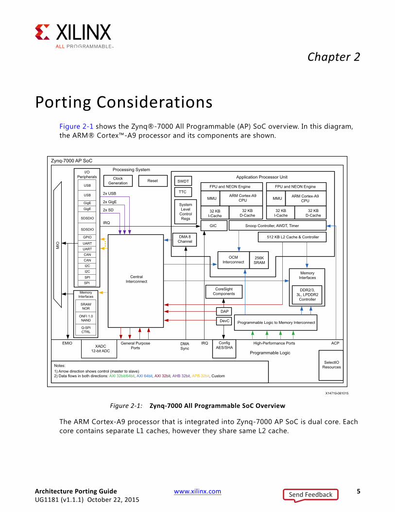
Porting ConsiderationsFigure 2-1 shows the Zynq®-7000 All Programmable (AP) SoC overview. In this diagram, the ARM® Cortex™-A9 processor and its components are shown.
The ARM Cortex-A9 processor that is integrated into Zynq-7000 AP SoC is dual core. Each core contains separate L1 caches, however they share same L2 cache.
X-Ref Target - Figure 2-1
Figure 2-1: Zynq-7000 All Programmable SoC Overview
Architecture Porting Guide www.xilinx.com 5UG1181 (v1.1.1) October 22, 2015
Send Feedback
Chapter 2: Porting Considerations
ARM Cortex-A9 FeaturesThe ARM processor features that must be considered are listed in the following sections.
CPU ModesAt any given time, the CPU can be in only one mode, but it can switch modes due to external events (interrupts) or programmatically.
• User mode: The only non-privileged mode.
• FIQ mode: A privileged mode that is entered whenever the processor accepts an FIQ interrupt.
• IRQ mode: A privileged mode that is entered whenever the processor accepts an IRQ interrupt.
• Supervisor (svc) mode: A privileged mode entered whenever the CPU is reset or when an SVC instruction is executed.
• Abort mode: A privileged mode that is entered whenever a prefetch abort or data abort exception occurs.
• Undefined mode: A privileged mode that is entered whenever an undefined instruction exception occurs.
• System mode (ARMv4 and above): The only privileged mode that is not entered by an exception. It can only be entered by executing an instruction that explicitly writes to the mode bits of the Current Program Status Register (CPSR).
• Monitor mode (ARMv6 and ARMv7 Security Extensions, ARMv8 EL3): A monitor mode is introduced to support TrustZone® extension in ARM cores.
• Hyp mode (ARMv7 Virtualization Extensions, ARMv8 EL2): A hypervisor mode that supports virtualization requirements for the non-secure operation of the CPU.
TrustZoneThe Security Extensions, marketed as TrustZone technology, is in Cortex-A9 architecture. It provides a low-cost alternative to adding another dedicated security core to an SoC by providing two virtual processors backed by hardware-based access control. This lets the application core switch between two states, referred to as worlds (to reduce confusion with other names for capability domains), to prevent information from leaking from the more trusted world to the less trusted world. This world switch is generally orthogonal to all other capabilities of the processor, thus each world can operate independently of the other while using the same core. Memory and peripherals are then made aware of the operating world of the core and can use this to provide access control to secrets and code on the device.
Architecture Porting Guide www.xilinx.com 6UG1181 (v1.1.1) October 22, 2015
Send Feedback

Chapter 2: Porting Considerations
Typical applications of TrustZone technology are to run a rich operating system in the less trusted world, and smaller security-specialized code in the more trusted world, allowing much tighter digital rights management (DRM) for controlling the use of media on ARM-based devices and preventing any unapproved use of the device. In practice, however, other silicon vendors besides Xilinx often treat specific implementation details of ARM TrustZone hardware and associated software as confidential information. Because of that, it might be unclear what types of services are being provided by such third-party solutions. Analyzing the software stack implementation can provide more information about the secure world implementation.
Typical Application Examples
Some common applications based on TrustZone are listed by ARM in their TrustZone website and give a quick understanding of real world TrustZone usage [Ref 3]:
• Secured PIN entry for enhanced user authentication in mobile payments and banking
• Protection against trojans, phishing and advanced persistent threats (APT)
• Enable deployment and consumption of high-value media (DRM)
• Bring your own device (BYOD) device persons and application separation
• Software license management
• Loyalty-based applications
• Access control of cloud-based documents
Thumb-2 Instruction SetIn Thumb state, the processor executes the Thumb instruction set, a compact 16-bit encoding for a subset of the ARM instruction set. Most of the Thumb instructions are directly mapped to normal ARM instructions. The space-saving comes from making some of the instruction operands implicit and limiting the number of possibilities compared to the ARM instructions executed in the ARM instruction set state.
In Thumb, the 16-bit opcodes have less functionality. For example, only branches can be conditional, and many opcodes are restricted to accessing only half of all of the CPU's general-purpose registers. The shorter opcodes give improved code density overall, even though some operations require extra instructions. In situations where the memory port or bus width is constrained to less than 32 bits, the shorter Thumb opcodes allow increased performance compared with 32-bit ARM code, because less program code might need to be loaded into the processor over the constrained memory bandwidth.
Thumb-2 extends the limited 16-bit instruction set of Thumb with additional 32-bit instructions to give the instruction set more breadth, thus producing a variable-length instruction set. A stated aim for Thumb-2 was to achieve code density similar to Thumb with performance similar to the ARM instruction set on 32-bit memory.
Architecture Porting Guide www.xilinx.com 7UG1181 (v1.1.1) October 22, 2015
Send Feedback
Chapter 2: Porting Considerations
SIMD Support (NEON)The Advanced SIMD extension (aka NEON Media Processing Engine (MPE)) is a combined 64- and 128-bit SIMD instruction set that provides standardized acceleration for media and signal processing applications. NEON is included in Cortex-A9 of Zynq-7000 AP SoC. It features a comprehensive instruction set, separate register f iles, and independent execution hardware. NEON supports 8-, 16-, 32-, and 64-bit integer and single-precision (32-bit) floating-point data and single instruction multiple data (SIMD) operations for handling audio and video processing as well as graphics and gaming processing. In NEON, the SIMD supports up to 16 operations at the same time. The NEON hardware shares the same floating-point registers as used in VFP. NEON can execute 128 bits at a time, however though the ARM Cortex-A9 processor supports 128-bit vectors it executes with 64 bits at a time. NEON can execute MP3 audio decoding on CPUs running at 10 MHz and can run the GSM adaptive multi-rate (AMR) speech codec at no more than 13 MHz.
Vector Floating-Point Unit (VFPU) - Single and Double PrecisionThis is the floating-point coprocessor extension to the ARM architecture.
Caches• L1 data cache 32 KB, L1 instruction cache 32 KB
° Both are separate, 4-way set associative
• L2 512 KB cache (common to data and instruction)
° 8-way set associative
MMUThe memory management unit (MMU) works with the L1 and L2 memory system to translate virtual addresses to physical addresses. It also controls accesses to and from external memory.
• Page table entries support 4 KB, 64 KB, 1 MB, and 16 MB.
• 16 domains.
• Global and application-specif ic identif iers remove the requirement for context switch translation look-aside buffer (TLB) flushes.
• Extended permissions check capability.
OCMThe on-chip memory (OCM) module contains 256 KB of RAM. It supports two 64-bit AXI slave interface ports, one dedicated to CPU/accelerator coherency port (ACP) access
Architecture Porting Guide www.xilinx.com 8UG1181 (v1.1.1) October 22, 2015
Send Feedback

Chapter 2: Porting Considerations
through the application processing unit (APU) snoop control unit (SCU), and the other shared by all other bus masters within the processing system (PS) and programmable logic (PL). The bootROM memory is used exclusively by the boot process and is not visible to the user.
The address range assigned to the OCM can be modified to exist in the f irst or last 256 KB of the address map, to flexibly handle the ARM low or high exception vector modes. In addition, the CPU and ACP AXI interfaces can have their lowest 1 MB address range accesses diverted to DDR, using the SCU address filtering feature.
Interrupts• Supported by Global Interrupt Controller (GIC) from ARM.
• 3 watch dog timers (WDTs)—1 for core0, 1 for core1, and 1 for system.
• Each core supports a few private peripheral interrupts (PPIs) and a few shared peripheral interrupts (SPIs).
• Interrupts can be prioritized.
• The CPU can go into a wait state (WFI) where it waits for an interrupt (or event) signal to be generated.
System Control Coprocessor (CP15)The system control coprocessor, CP15, controls and provides status information for the functions implemented in the processor. The main functions of the system control coprocessor are:
• Overall system control and configuration
• MMU configuration and management
• Cache configuration and management
• System performance monitoring
TimersEach Cortex-A9 processor core has its own private 32-bit timer and 32-bit watchdog timer. Both processor cores share a global 64-bit timer.
All these timers are always clocked at 1/2 of the CPU frequency (CPU_3x2x).
On the system level, there is a 24-bit watchdog timer and two 16-bit triple timer/counters. The system watchdog timer is clocked at 1/4 or 1/6 of the CPU frequency (CPU_1x), or can be clocked by an external signal from an MIO pin or from the PL.
Architecture Porting Guide www.xilinx.com 9UG1181 (v1.1.1) October 22, 2015
Send Feedback
Chapter 2: Porting Considerations
The two triple timers/counters are always clocked at 1/4 or 1/6 of the CPU frequency (CPU_1x), and are used to count the widths of signal pulses from an MIO pin or from the PL.
Instruction SetThe ARM is a reduced instruction set computer (RISC) processor. The instruction set has the following features:
• Load/store architecture.
• Supports unaligned accesses for half-word and single-word load/store instructions with some limitations, such as no guaranteed atomicity.
• Uniform 16 × 32-bit register f ile (including the Program Counter, Stack Pointer, and the Link Register).
• Fixed instruction width of 32 bits to ease decoding and pipelining, at the cost of decreased code density.
• The Thumb instruction set added 16-bit instructions and increased code density.
• Mostly single clock-cycle execution.
To compensate for the simpler design, compared with architectures like Intel, some additional design features were used:
• Conditional execution of most instructions reduces branch overhead and compensates for the lack of a branch predictor.
• Arithmetic instructions alter condition codes only when desired.
• 32-bit barrel shifter can be used without performance penalty with most arithmetic instructions and address calculations.
• Powerful indexed addressing modes.
• A link register supports fast leaf function calls.
• A simple but fast 2-priority-level interrupt subsystem has switched register banks.
Architecture Porting Guide www.xilinx.com 10UG1181 (v1.1.1) October 22, 2015
Send Feedback

Chapter 2: Porting Considerations
Register SetThe register set is listed in the following table.
Registers R0 through R7 are the same across all CPU modes; they are never banked.
R13 and R14 are banked across all privileged CPU modes except System mode. That is, each mode that can be entered because of an exception has its own R13 and R14. These registers generally contain the stack pointer and the return address from function calls, respectively.
Aliases
• R13 is also referred to as SP, the Stack Pointer.
• R14 is also referred to as LR, the Link Register.
• R15 is also referred to as PC, the Program Counter.
Registers Across CPU Modes
usr sys svc abt und irq fiq
R0
R1
R2
R3
R4
R5
R6
R7
R8 R8_fiq
R9 R9_fiq
R10 R10_fiq
R11 R11_fiq
R12 R12_fiq
R13 R13_svc R13_abt R13_und R13_irq R13_fiq
R14 R14_svc R14_abt R14_und R14_irq R14_fiq
R15
CPSR
SPSR_svc SPSR_abt SPSR_und SPSR_irq SPSR_fiq
Architecture Porting Guide www.xilinx.com 11UG1181 (v1.1.1) October 22, 2015
Send Feedback
Chapter 2: Porting Considerations
The Current Program Status Register (CPSR) has the following 32 bits:
• M (bits 0-4) is the processor mode bits.
• T (bit 5) is the Thumb state bit.
• F (bit 6) is the FIQ disable bit.
• I (bit 7) is the IRQ disable bit.
• A (bit 8) is the imprecise data abort disable bit.
• E (bit 9) is the data endianness bit.
• IT (bits 10-15 and 25-26) is the if-then state bits.
• GE (bits 16-19) is the greater-than-or-equal-to bits.
• DNM (bits 20-23) is the do not modify bits.
• J (bit 24) is the Java state bit.
• Q (bit 27) is the sticky overflow bit.
• V (bit 28) is the overflow bit.
• C (bit 29) is the carry/borrow/extend bit.
• Z (bit 30) is the zero bit.
• N (bit 31) is the negative/less than bit.
When you plan to move software from other architectures to ARM, there are certain mandatory and optional considerations, which are described in the next chapter.
Architecture Porting Guide www.xilinx.com 12UG1181 (v1.1.1) October 22, 2015
Send Feedback
Chapter 3
Feature Comparison Across Architectures
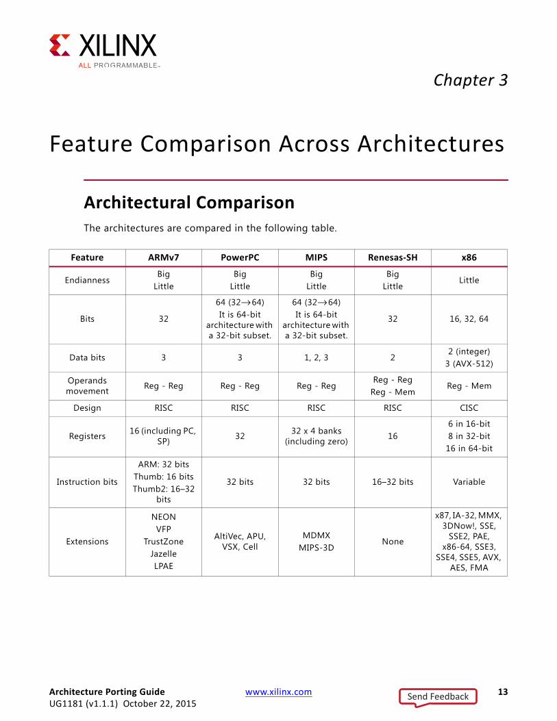
Architectural ComparisonThe architectures are compared in the following table.
Feature ARMv7 PowerPC MIPS Renesas-SH x86
EndiannessBig
LittleBig
LittleBig
LittleBig
LittleLittle
Bits 32
64 (32→64)It is 64-bit
architecture with a 32-bit subset.
64 (32→64)It is 64-bit
architecture with a 32-bit subset.
32 16, 32, 64
Data bits 3 3 1, 2, 3 22 (integer)
3 (AVX-512)
Operands movement Reg - Reg Reg - Reg Reg - Reg
Reg - RegReg - Mem
Reg - Mem
Design RISC RISC RISC RISC CISC
Registers 16 (including PC, SP) 32 32 x 4 banks
(including zero) 166 in 16-bit8 in 32-bit
16 in 64-bit
Instruction bits
ARM: 32 bitsThumb: 16 bitsThumb2: 16–32
bits
32 bits 32 bits 16–32 bits Variable
Extensions
NEONVFP
TrustZoneJazelleLPAE
AltiVec, APU, VSX, Cell
MDMXMIPS-3D
None
x87, IA-32, MMX, 3DNow!, SSE,
SSE2, PAE, x86-64, SSE3,
SSE4, SSE5, AVX, AES, FMA
Architecture Porting Guide www.xilinx.com 13UG1181 (v1.1.1) October 22, 2015
Send Feedback
Chapter 3: Feature Comparison Across Architectures
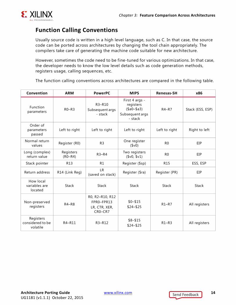
Function Calling ConventionsUsually source code is written in a high level language, such as C. In that case, the source code can be ported across architectures by changing the tool chain appropriately. The compilers take care of generating the machine code suitable for new architecture.
However, sometimes the code need to be fine-tuned for various optimizations. In that case, the developer needs to know the low level details such as code generation methods, registers usage, calling sequences, etc.
The function calling conventions across architectures are compared in the following table.
Convention ARM PowerPC MIPS Renesas-SH x86
Function parameters R0–R3
R3–R10Subsequent args
- stack
First 4 args - registers ($a0–$a3)
Subsequent args - stack
R4–R7 Stack (ESS, ESP)
Order of parameters
passedLeft to right Left to right Left to right Left to right Right to left
Normal return values Register (R0) R3 One register
($v0) R0 EIP
Long (complex) return value
Registers (R0–R4) R3–R4 Two registers
($v0, $v1) R0 EIP
Stack pointer R13 R1 Register ($sp) R15 ESS, ESP
Return address R14 (Link Reg) LR (saved on stack) Register ($ra) Register (PR) EIP
How local variables are
locatedStack Stack Stack Stack Stack
Non-preserved registers R4–R8
R0, R2–R10, R12FPR0–FPR13LR, CTR, XER,
CR0–CR7
$0–$15$24–$25
R1–R7 All registers
Registers considered to be
volatileR4–R11 R3–R12
$8–$15$24–$25
R1–R3 All registers
Architecture Porting Guide www.xilinx.com 14UG1181 (v1.1.1) October 22, 2015
Send Feedback

Chapter 3: Feature Comparison Across Architectures
Setting Up For and Cleaning Up After a Function CallThe RISC processors (ARM, MIPS, PowerPC, and Renesas-SH) follow the standards ABI/EABI (1) for the function calling sequence, but with minor differences. Table 3-1 lists the calling procedure for each architecture.
1. application binary interface/embedded-application binary interface
Table 3-1: Function Calling Procedure for Each Architecture
Architecture Prologue (prepare to invoke function call) Epilogue (prepare to exit function call)
ARM
Push r4 to r11 to the stack.Push the return address in r14, to the stack.Copy args (r0–r3) to the local scratch regs (r4–r11).Allocate other local variables to the remaining local scratch regs (r4 to r11).Call other subroutines as necessary using BL.
Put the result in r0.Pull r4 to r11 from the stack.Pull the return address to the program counter r15.
MIPS
Reserve space for the stack frame. The stack frame can have 5 sections maximum:• Argument section,• Saved register section• Return address section• Padding section• Local data storage section.Set up a virtual frame pointer. The virtual frame pointer is sp($29) added to the frame size.Set a bit in the bitmask for each general purpose register saved.Store any registers that need to be saved.Set instruction pointer to function beginning.Start executing the function.
Place result in $v0.Issue a restore for each register saved in the prologue.Return from the procedure.
Architecture Porting Guide www.xilinx.com 15UG1181 (v1.1.1) October 22, 2015
Send Feedback

Chapter 3: Feature Comparison Across Architectures
PowerPC
Called function is responsible for allocating its own stack frame, making sure to preserve 16-byte alignment in the stack.Decrements the stack pointer to account for the new stack frame and writes the previous value of the stack pointer to its own linkage area, which ensures the stack can be restored to its original state after returning from the call.Saves all nonvolatile general purpose and floating-point registers into the saved registers area.Saves the link register and condition register values in the caller's linkage area, if needed.The stack frame contain four sections, in the following order:• Parameter area• Linkage area• Saved registers• Local variablesExecute the function code.
Restores the nonvolatile general purpose and floating-point registers that were saved in the stack frame.Nonvolatile registers are saved in the new stack frame before the stack pointer is updated, only when they f it within the space beneath the stack pointer, where a new stack frame would normally be allocated, also known as the red zone. The red zone is, by definition, large enough to hold all nonvolatile general purpose and floating-point registers but not the nonvolatile vector registers.Restores the condition register and link register values that were stored in the linkage area.Restores the stack pointer to its previous value.Returns control to the calling routine using the address stored in the link register.
x86
Pushes the old base pointer onto the stack.Gets new base pointer value which is set in the next step and is always pointed to this location.Assigns the value of stack pointer (which is pointed to the saved base pointer and the top of the old stack frame) into base pointer such that a new stack frame is created on top of the old stack frame (i.e., the top of the old stack frame becomes the base of the new stack frame).Moves the stack pointer further. The stack pointer is decreased to make room for variables (i.e., the function's local variables).Executes the function code.
Replaces the stack pointer with the current base (or frame) pointer, so the stack pointer is restored to its value before the prologue.Pops the base pointer off the stack, so it is restored to its value before the prologue.Returns to the calling function by popping the previous frame's program counter off the stack and jumping to it.
Renesas-SH
A sequence of zero or more instructions that save the incoming argument values from R4–R7 and FR4–FR11 to the argument home locations.A sequence of zero or more instructions that push all permanent registers to be saved and the return address (PR).A sequence of one or more instructions that set up the frame pointer.A sequence of zero or more instructions that allocate the remaining stack frame space for local variables, compiler-generated temporaries, and the argument-build area by subtracting a 4-byte aligned offset from R15.Execute the function code.
A single add instruction that increments the frame pointer.A sequence of instructions that modify R15 by referencing it in the destination operand of the instruction or in a post-increment memory address operand of the instruction.
Table 3-1: Function Calling Procedure for Each Architecture (Cont’d)
Architecture Prologue (prepare to invoke function call) Epilogue (prepare to exit function call)
Architecture Porting Guide www.xilinx.com 16UG1181 (v1.1.1) October 22, 2015
Send Feedback
Chapter 3: Feature Comparison Across Architectures
The following sections describe architectural considerations.
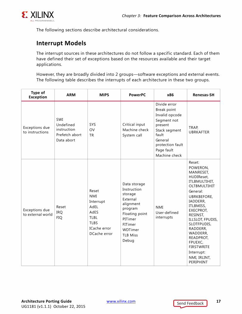
Interrupt ModelsThe interrupt sources in these architectures do not follow a specif ic standard. Each of them have defined their set of exceptions based on the resources available and their target applications.
However, they are broadly divided into 2 groups—software exceptions and external events. The following table describes the interrupts of each architecture in these two groups.
Type of Exception ARM MIPS PowerPC x86 Renesas-SH
Exceptions due to instructions
SWIUndefined instructionPrefetch abortData abort
SYSOVTR
Critical inputMachine checkSystem call
Divide errorBreak pointInvalid opcodeSegment not presentStack segment faultGeneral protection faultPage faultMachine check
TRAP, UBRKAFTER
Exceptions due to external world
ResetIRQFIQ
ResetNMIInterruptAdELAdESTLBLTLBSICache errorDCache error
Data storageInstruction storageExternal alignment programFloating pointPITimerFITimerWDTimerTLB MissDebug
NMIUser-defined interrupts
Reset:POWERON, MANRESET, HUDIReset, ITLBMULTIHIT, OLTBMULTIHITGeneral:UBRKBEFORE, IADDERR, ITLBMISS, EXECPROT, RESINST, ILLSLOT, FPUDIS, SLOTFPUDIS, RADDERR, WADDERR, READPROT, FPUEXC, FIRSTWRITEInterrupt:NMI, IRLINT, PERIPHINT
Architecture Porting Guide www.xilinx.com 17UG1181 (v1.1.1) October 22, 2015
Send Feedback
Chapter 3: Feature Comparison Across Architectures
Address Maps
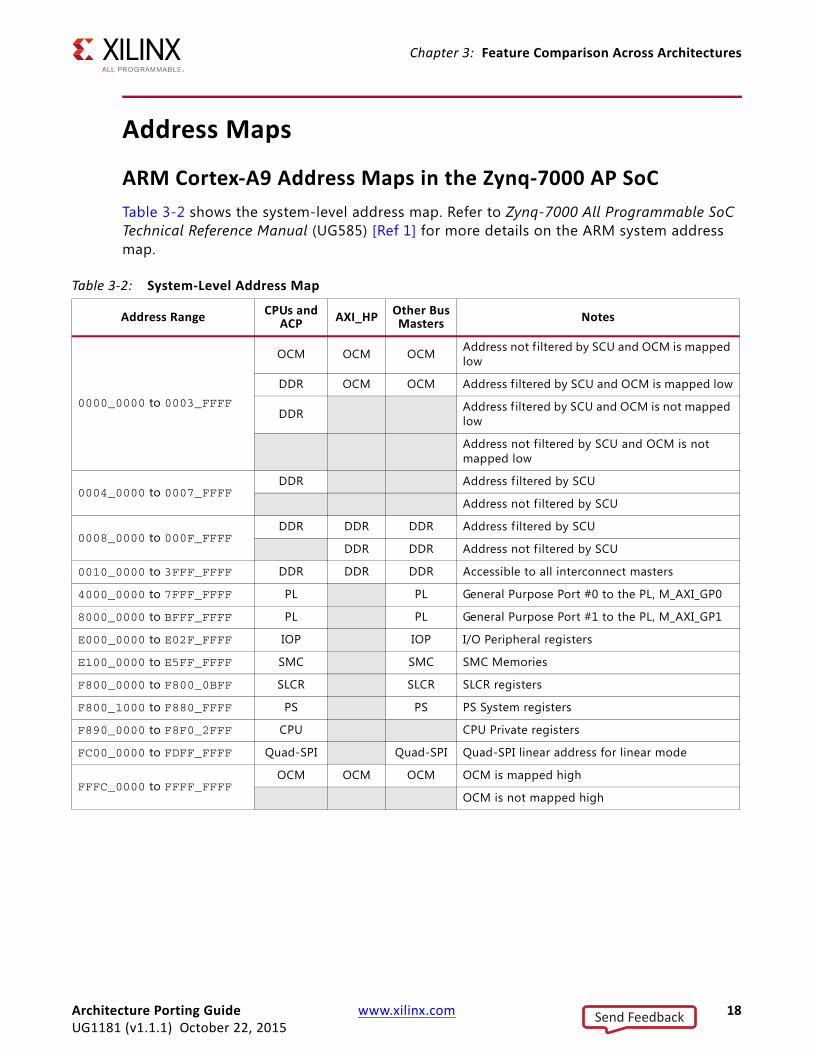
ARM Cortex-A9 Address Maps in the Zynq-7000 AP SoCTable 3-2 shows the system-level address map. Refer to Zynq-7000 All Programmable SoC Technical Reference Manual (UG585) [Ref 1] for more details on the ARM system address map.
Table 3-2: System-Level Address Map
Address Range CPUs and ACP AXI_HP Other Bus
Masters Notes
0000_0000 to 0003_FFFF
OCM OCM OCM Address not f iltered by SCU and OCM is mapped low
DDR OCM OCM Address f iltered by SCU and OCM is mapped low
DDR Address f iltered by SCU and OCM is not mapped low
Address not f iltered by SCU and OCM is not mapped low
0004_0000 to 0007_FFFF DDR Address f iltered by SCU
Address not f iltered by SCU
0008_0000 to 000F_FFFFDDR DDR DDR Address f iltered by SCU
DDR DDR Address not f iltered by SCU
0010_0000 to 3FFF_FFFF DDR DDR DDR Accessible to all interconnect masters
4000_0000 to 7FFF_FFFF PL PL General Purpose Port #0 to the PL, M_AXI_GP0
8000_0000 to BFFF_FFFF PL PL General Purpose Port #1 to the PL, M_AXI_GP1
E000_0000 to E02F_FFFF IOP IOP I/O Peripheral registers
E100_0000 to E5FF_FFFF SMC SMC SMC Memories
F800_0000 to F800_0BFF SLCR SLCR SLCR registers
F800_1000 to F880_FFFF PS PS PS System registers
F890_0000 to F8F0_2FFF CPU CPU Private registers
FC00_0000 to FDFF_FFFF Quad-SPI Quad-SPI Quad-SPI linear address for linear mode
FFFC_0000 to FFFF_FFFF OCM OCM OCM OCM is mapped high
OCM is not mapped high
Architecture Porting Guide www.xilinx.com 18UG1181 (v1.1.1) October 22, 2015
Send Feedback

Chapter 3: Feature Comparison Across Architectures
MIPSFigure 3-1 describes the MIPS memory map.
X-Ref Target - Figure 3-1
Figure 3-1: MIPS Memory Map
Architecture Porting Guide www.xilinx.com 19UG1181 (v1.1.1) October 22, 2015
Send Feedback
Chapter 3: Feature Comparison Across Architectures
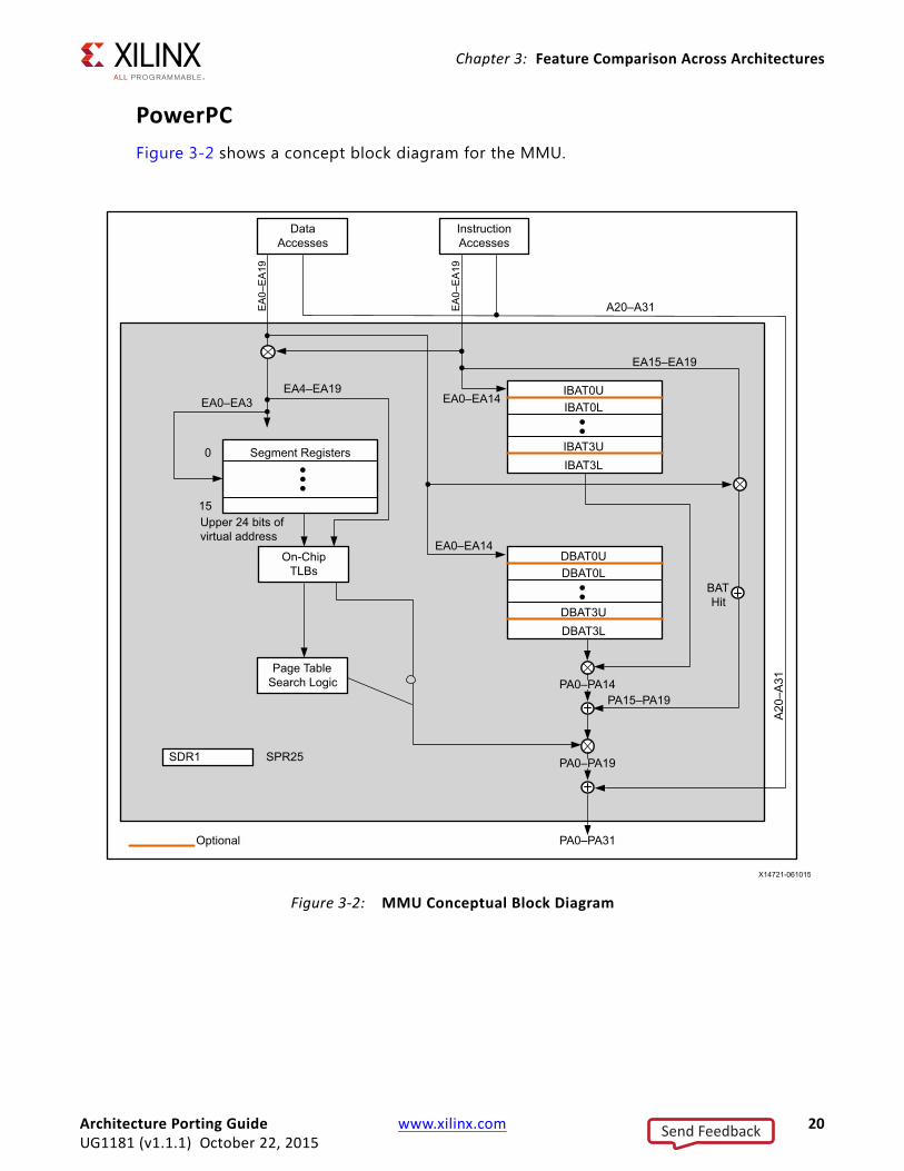
PowerPCFigure 3-2 shows a concept block diagram for the MMU.
X-Ref Target - Figure 3-2
Figure 3-2: MMU Conceptual Block Diagram
Architecture Porting Guide www.xilinx.com 20UG1181 (v1.1.1) October 22, 2015
Send Feedback

Chapter 3: Feature Comparison Across Architectures
x86Figure 3-3 describes the x86 address mechanism.
X-Ref Target - Figure 3-3
Figure 3-3: x86 Address Mechanism
Architecture Porting Guide www.xilinx.com 21UG1181 (v1.1.1) October 22, 2015
Send Feedback
Chapter 3: Feature Comparison Across Architectures
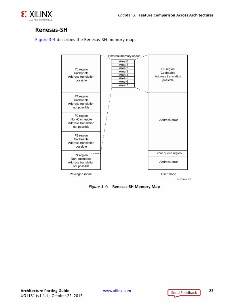
Renesas-SHFigure 3-4 describes the Renesas-SH memory map.
X-Ref Target - Figure 3-4
Figure 3-4: Renesas-SH Memory Map
Architecture Porting Guide www.xilinx.com 22UG1181 (v1.1.1) October 22, 2015
Send Feedback

Chapter 3: Feature Comparison Across Architectures
Register SetsThe following table lists major features of register sets for ARM, MIPS, PowerPC, x86, and Renesas-SH processors.
Register Type ARM MIPS PowerPC x86 Renesas-SH
General purpose registers R0–R12
$8–$15, $24, $25: temporary (not saved)$16–$23: temporary (saved)
User model (UISA)GPR0-31FPR0-31CRFPSCRXERLRCTRTBU/TBL
General: EAX, EBX, ECX, EDXSegment: CS, DS, ES, FS, GS, SSIndex: ESI, EDI, EBP, EIP, ESPIndicator: EFLAGS
General, banked: R0–R7General, non-banked: R8-R15Floating, banked: FR0-15, XF0-15
Specific usage registers
R13: stack pointerR14: link registerR15: program counter
$0: wired to zero$1: reserved for assembler$2, $3: function return values$4-$7: function arguments$26, $27: reserved for OS$28: global pointer$29: stack pointer$30: frame pointer (saved)$31: link register
None None
Control registers: SR, GBR, SSR, SPC, SGR, DBR, VBRSystem registers: MACH, MACL, PR, FUPL, PC, FPSCR
Special purpose registers
System coprocessor CP15
$SR, $PC, GBR, VBR, SGR, DBR, MACL, MACH, PR, PC, FPUL, FPSCR, TRA, EXPEVT, INTEVT, PTEH, PTEL, TTB, TEA, MMUCR, PASCR, IRMCR, CCR, QACR0/1, RAMCR, LSA0/1, LDA0/1, CPUPOM, PVR
Supervisor mode (OEA)MSRPVRSDR1ASRDARDSISRSRR0-1SPRG0-3FPECRDABRDECEARPIR
Control: CR0-4Debug: DR0-7Test: TR0-7GDTR, IDTR, LDTR, TR
None
Architecture Porting Guide www.xilinx.com 23UG1181 (v1.1.1) October 22, 2015
Send Feedback

Chapter 3: Feature Comparison Across Architectures
Detailed Porting Guides: MIPS, PowerPC, Intel, and RenesasWhen considering porting to a Xilinx Zynq-7000 device, which is an ARM Cortex-A9 based SoC, see UltraFast Embedded Design Methodology Guide (UG1046) [Ref 2], which contains details about:
• System level considerations
• Hardware design considerations
• Software design considerations
• Hardware design flow
• Software design flow
• Debugging techniques
• SDSoC environment
This methodology guide supports porting user applications from non-ARM platforms to the ARM platform.
Port from MIPS to ARMFor a detailed explanation, see Migrating from MIPS to ARM at the ARM site.
Port from PowerPC to ARMFor a detailed explanation, see Migrating from Power Architecture to ARM at the ARM site.
Port from Intel IA-32 to ARMFor a detailed explanation, see Migrating from IA-32 to ARM at the ARM site.
Port from Renesas-SH to ARMFor a detailed explanation, see AN314 Migrating from SH-4A to Cortex-A at the ARM site.
Architecture Porting Guide www.xilinx.com 24UG1181 (v1.1.1) October 22, 2015
Send Feedback
Appendix A
Additional Resources and Legal Notices
Xilinx ResourcesFor support resources such as Answers, Documentation, Downloads, and Forums, see Xilinx Support.
Solution CentersSee the Xilinx Solution Centers for support on devices, software tools, and intellectual property at all stages of the design cycle. Topics include design assistance, advisories, and troubleshooting tips.
References1. Zynq-7000 All Programmable SoC Technical Reference Manual (UG585)
2. UltraFast Embedded Design Methodology Guide (UG1046)
3. ARM TrustZone Technology (www.arm.com/products/processors/technologies/trustzone/index.php)
Please Read: Important Legal NoticesThe information disclosed to you hereunder (the “Materials”) is provided solely for the selection and use of Xilinx products. To the maximum extent permitted by applicable law: (1) Materials are made available "AS IS" and with all faults, Xilinx hereby DISCLAIMS ALL WARRANTIES AND CONDITIONS, EXPRESS, IMPLIED, OR STATUTORY, INCLUDING BUT NOT LIMITED TO WARRANTIES OF MERCHANTABILITY, NON-INFRINGEMENT, OR FITNESS FOR ANY PARTICULAR PURPOSE; and (2) Xilinx shall not be liable (whether in contract or tort, including negligence, or under any other theory of liability) for any loss or damage of any kind or nature related to, arising under, or in connection with, the Materials (including your use of the Materials), including for any direct, indirect, special, incidental, or consequential loss or damage (including loss of data, profits, goodwill, or any type of loss or damage suffered as a result of any action brought by a third party) even if such damage or loss was reasonably foreseeable or Xilinx had been advised of the possibility of the same. Xilinx assumes no obligation to correct any errors contained in the Materials or to notify you of updates to the Materials or to product specifications. You may not reproduce, modify, distribute, or publicly display the Materials without prior written consent. Certain products are subject to the terms and conditions of Xilinx’s limited warranty, please refer to Xilinx’s Terms of Sale which can be viewed at http://www.xilinx.com/legal.htm#tos; IP cores may be subject to warranty and support terms contained in a license issued to you by Xilinx. Xilinx products are not designed or intended to be
Architecture Porting Guide www.xilinx.com 25UG1181 (v1.1.1) October 22, 2015
Send Feedback
fail-safe or for use in any application requiring fail-safe performance; you assume sole risk and liability for use of Xilinx products in such critical applications, please refer to Xilinx’s Terms of Sale which can be viewed at http://www.xilinx.com/legal.htm#tos.Automotive Applications Disclaimer XILINX PRODUCTS ARE NOT DESIGNED OR INTENDED TO BE FAIL-SAFE, OR FOR USE IN ANY APPLICATION REQUIRING FAIL-SAFE PERFORMANCE, SUCH AS APPLICATIONS RELATED TO: (I) THE DEPLOYMENT OF AIRBAGS, (II) CONTROL OF A VEHICLE, UNLESS THERE IS A FAIL-SAFE OR REDUNDANCY FEATURE (WHICH DOES NOT INCLUDE USE OF SOFTWARE IN THE XILINX DEVICE TO IMPLEMENT THE REDUNDANCY) AND A WARNING SIGNAL UPON FAILURE TO THE OPERATOR, OR (III) USES THAT COULD LEAD TO DEATH OR PERSONAL INJURY. CUSTOMER ASSUMES THE SOLE RISK AND LIABILITY OF ANY USE OF XILINX PRODUCTS IN SUCH APPLICATIONS.© Copyright 2015 Xilinx, Inc. Xilinx, the Xilinx logo, Artix, ISE, Kintex, Spartan, Virtex, Vivado, Zynq, and other designated brands included herein are trademarks of Xilinx in the United States and other countries. ARM is a registered trademark of ARM in the EU and other countries. The PowerPC name and logo are registered trademarks of IBM Corp. and used under license. All other trademarks are the property of their respective owners.
Architecture Porting Guide www.xilinx.com 26UG1181 (v1.1.1) October 22, 2015
Send Feedback