zeiss orionplus - trinity college, dublin · helium ion beams – is subject to a beam scattering...
TRANSCRIPT

C a r l Z e i s s S M T – N a n o T e c h n o l o g y S y s t e m s D i v i s i o n
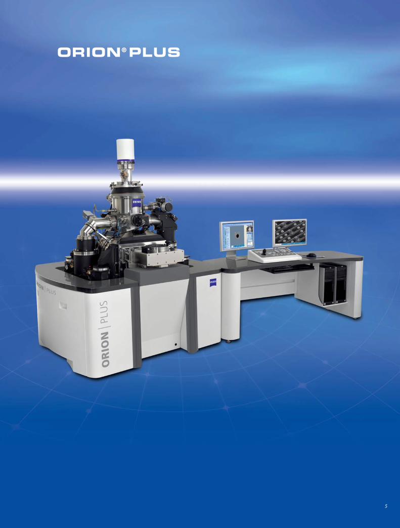
ZEISS ORION®PLUS
The revolutionary helium ion microscopefor cutting edge imaging applications,providing ultra high resolution coupledwith unique material contrast.
D I S C O V E R N E W H O R I Z O N S I N
N A N O S C A L E I M A G I N G
E n a b l i n g t h e N a n o - A g e W o r l d ®
We make it visible.

ORION®PLUSSee things you could never see before.Superior to scanning electron microscopes, the ORION®PLUS helium ionmicroscope delivers ultra-high resolutionimaging with strong material contrast.
2

ORION®PLUS
See a new world record resolution for any ScanningIon/Electron Microscope. This resolution breakthroughof 0.24nm was achieved onan asbestos sample on aholey carbon film and repre-sents achievable performanceof this machine on bulk samples.
See material contrast likeyou've never seen before.With a higher, more variedsecondary electron yield, your images are sharp, clear and bright.
See low-Z materials, like biological materials, with resolution and surfaceinformation unavailablefrom a typical SEM.
See Chrome lines on quartzsubstrate demonstrating theability to inspect and charac-terize highly charging samplesat highest resolution.
World Record Resolution changes microscopy paradigm.
3

Concept
The ZEISS ORION® PLUS microscope is based on the
revolutionary, atomic-sized, ALIS gas field ion source.
The “Trimer”
The secret to the amazing resolving power of the helium
ion beam starts with the source tip. A finely sharpened
needle is made even sharper through a proprietary
process. Individual atoms are stripped away from the
source until an atomic pyramid is created with just three
atoms at the very end of the source tip – a configuration
called the "trimer". This repeatable process can be
accomplished in-situ.
Once the trimer is formed, the tip is maintained under
high vacuum and cryogenic temperatures with helium gas
flowing over it. A high voltage is applied to the needle
to produce an extremely high electric field at its apex.
The helium gas is attracted to the energized tip where it
is ionized. With ionization happening in the vicinity of a
single atom, the resulting ion beam appears to be emana-
ting from a region that is less than an angstrom in size.
This produces an extremely bright beam that can be
focused to an extraordinarily small probe size.
The Column
This ALIS source is mated with an advanced electrostatic
ion column that focuses the beam with sub-nanometer
precision. Much like a SEM, the beam is rastered across
the sample pixel by pixel.
Imaging
The number of detected secondary electrons is used to
determine the gray level of that particular pixel. Since the
number of detected secondary electrons varies with
material composition and shape, the images provide
excellent topographic and compositional information.
Diffraction
Helium ions are about 8000 times heavier than electrons.
Because of this, a helium ion beam exhibits very little
diffraction when passed through an aperture or across
an edge. Diffraction is a significant problem for a SEM
where the diffraction effect limits its ultimate spot size.
Since the helium ion beam is not affected by diffraction,
it can be focused to a much finer spot size, enabling
sub-nanometer resolution.
Long Source Lifetime
The helium ion source has a very long lifetime due to
the fact that the source tip is always kept at a positive
potential. The only things attracted to the tip are elec-
trons, which do not cause any ill effects. Positively
charged ions are repelled from the tip and other gasses
will be ionized before they have a chance to strike the
source tip. For this reason, the source lifetime for the
helium ion source is well over 1000 hours.
ORION®PLUS – powered by ZEISS ALIS Source Technology
4
Image of the atoms at the end of the source tipemitting helium ions.Since each atom can beindividually seen, the virtual source size mustbe much smaller.
The helium ion beam has a DeBroglie wavelength that is approximately 300 timessmaller than an electron beam resulting in much less diffraction.
5
ORION®PLUS

6
ORION®PLUSSource
Imaging Gas
Extractor
Focus
Ion Beam
Aperture
ScanningDeflectors
Display
Transmission Detector
Electron Detector Ion Detector
FinalLens

Beam Scattering
Imaging with charged particle beams – either electron or
helium ion beams – is subject to a beam scattering effect.
When the beam's primary particles strike the sample sur-
face, they interact with the surrounding material, causing
the emission of secondary electrons from an area that is
somewhat larger than the size of the beam itself. The
larger the area of surface interaction, the lower is the
ultimate imaging resolution. Conversely, the smaller the
area of surface interaction, the higher will be the ulti-
mate image resolution.
In the case of a SEM, the beam's electrons are scattered
rapidly in the sample, resulting in secondary electrons
being emitted from an area many times larger than the
beam itself. Fortunately, when the helium ion beam strikes
the sample with its larger and heavier particles, the
particles do not scatter near the surface. This translates
into a smaller area of surface interaction and much higher
resolution images for the helium ion microscope.
Material Contrast
Although the area of surface interaction for the helium ion
beam is relatively small – compared to a typical SEM, the
total number of secondary electrons produced is greater.
This larger secondary electron yield, and the large dif-
ference in yield between different materials, provides
higher contrast imaging, making it easier to differentiate
between materials with the helium ion microscope.
In addition, the helium ion microscope can collect back-
scattered helium ions, much like in Rutherford Backscat-
tered Spectroscopy. With proper selection and positioning
of the detector, the total backscattered ion yield is direct-
ly proportional to the mass of the sample atoms. Using
this imaging mode, it is possible to easily differentiate
between sample materials.
7
ORION®PLUS – Surface Interaction and Contrast
Focused Beam of Electrons
SEM Focused Beam of Helium Ions
HIM
Secondary Electron Yield
Secondary Electron Yield
Area ofSurfaceInteraction
Area ofSurfaceInteraction
Excited Volume Excited Volume
Material Z M(amu) SE yield
Aluminum
Silicon
Titanium
Iron
Nickel
Copper
Indium
Tungsten
Rhenium
Platinum
Gold
Lead
13
14
22
26
28
29
49
74
75
78
79
82
27.0
28.1
47.9
55.8
58.7
63.4
114.8
183.8
186.2
195.1
197.0
207.2
5.31
3.38
4.65
4.55
5.14
4.23
5.69
3.69
3.61
8.85
5.17
5.57

8
ORION®PLUS – Unique Features
Since the ORION® was introduced, a number of
new features have been developed that have
further enhanced the image quality from the
Helium Ion Microscope. The main ones are:
“Accelerating Voltage” – the tip geometry has
been modified to increase the accelerating
voltage of the helium ions resulting in improved
resolution.
"Clear View" – an active sample cleaning system
which is a combination of plasma cleaning,
heating elements, and an in-situ vapor clean that
removes hydrocarbons from the sample and the
environment and prevents re-deposition in the
scanned area. This results in images with
increased surface detail and is ideal for
semiconductor samples. This also reduces the
need for external sample cleaners.
"Signal Boost" – enhances secondary electron
collection at short working distances resulting
inimproved signal to noise.
"Quiet Mode" Imaging – with a cryo-
mechanical pump for cooling the source (instead
of liquid Nitrogen), the user can minimize the
external environmental influence and acquire
noise free images. An additional benefit of this
is the lower source temperature which results in
an increase in brightness.
“Ease of Use” – software enhancements for
increased ease of use. 4x improvement in signal collection at 4mm working distance.
Inside schematic of the ORION® PLUS work chamber showing the electron (ET) and ion (MCP) detectors, as well as the charge neutralizingflood gun. These features provide the different imaging modes and sample type flexibility that are designed into the microscope.
300 nm FOV
ET detector
Flood gun
MCP detector

9
Insulating Samples
The image at the right is of collagen fibrils from the knee
joint of a mouse. The sample is insulating and high
resolution imaging in SEMs is difficult without coating
the sample. In the ORION® PLUS, charge compensation is
performed with an electron flood gun which neutralizes
the positive charge induced by the helium ion beam. The
ORION® PLUS image clearly shows the bands which are
61 nm apart.
Low-Z Materials
Many low-Z materials are challenging to image in a
conventional SEM as the electrons tend to pass right
through the substrate and fail to provide much useful
imaging information. The more massive helium ions have
greater stopping power in low-Z materials and provide
copious amounts of useful secondary electrons for high
contrast images such as the ones seen at right of carbon
nanotubes.
Biological Materials
The ability to image samples prone to damage as well
as bring out subtle changes in contrast make the
ORION® PLUS an ideal tool for imaging biological samples.
The image on the right shows Philipodia from Chinese
Hamster Ovary cells highlighting the ORION® PLUS' ability
to preserve the structural integrity of delicate frameworks
while creating a high contrast image.
Superior Material Contrast
The helium ion ORION® PLUS microscope has unsurpassed
material contrast. The image on the right of a flash
memory cell shows clear differentiation between the
various layers highlighting the surface sensitivity of the
ORION® PLUS at a high magnification.
ORION®PLUS – Applications
Sample courtesy of Dr. Brendan Griffin, University of Western Australia.
Sample courtesy of NMI.
Sample courtesy of Chipworks.
Collagen fibers from theknee joint of a mouse. The banding in the fibersis clearly seen. The chargeneutralizing flood gunavailable in theORION® PLUS allows for stable imaging. Imaging in collaborationwith Dr. Claus Burkhardt,NMI (Stuttgart, Germany)

10
ORION®PLUS – Applications
The articulation of the dielectric barrier (high performance insulator) seen lining this DRAM trench attests to the strength of ORION® PLUS when spotlighting contrast between materials.Sample courtesy of Infineon.
Transmission mode imaging of an IC device on the ORION® PLUSshows the aluminum metal line with its Titanium-Tungsten liners and Tungsten via. The image reveals the aluminum grainstructure as well as Micro-structure defects in the core of theTungsten plug.Sample courtesy of Fraunhofer Institute, Halle.
Semiconductor Applications
The ORION® PLUS provides unique contrast mechanisms
which make it the tool of choice for semiconductor
applications. In addition to fine surface detail, the
ORION® PLUS can image dopant profile without any
additional sample preparation. Further, the strong
material contrast shows interface layers a few nm thick
in stunning detail.
Deprocessed 65 nm CMOS SRAM device at the contact level highlighting the material contrast, surface sensitivity, and topographic detail obtained in the ORION® PLUS.
Patterned NBPT self assembled monolayer on gold. An ebeamstencil mask converted the terminal group of the exposed from anitrate group to an amine. This alteration is invisible to the SEMbut is captured clearly in ORION® PLUS.Sample courtesy of University of Bielefeld (Germany)

11
Technical Data
ORION® PLUSEssential Specifications
Resolution (Probe Size)
Accelerating Voltage
Magnification
Field of View
Ion Beam
Ion Source
Process Chamber
Sample Cleaning
Image Detectors
Sample Stage
Vacuum System
Video Cameras
User Interface
≤ 0.75 nm
30 kV ± 5 kV (fixed)
100 x – 1,000,000 x
1mm – 100 nm
Range: 1 fA - 100 pA
Typical Imaging: 0.5 pA - 1 pA @ highest resolution
Standard Test: > 5 pA
Helium Gas Field Ion Source
Lifetime > 1000 hours
Volume 400 mm3
Base Vacuum 8 x 10⁻⁷ Torr
Customizable port plate
Loadlock
Loadlock: Integrated Plasma Cleaner
Chamber: Gas based Active Sample Cleaner
Everhart-Thornley
Microchannel Plate
5-axis motorized stage, 50 mm travel in X and Y, 12 mm Z, 360°,
0° to 45°tilt
Oil and particle free roughing pump design
300 L/sec Mag-Lev turbomolecular pumps
Two video monitoring cameras – Source View and Chamber View
Two Intel® Dual Core Xeon Processors
2GB DDR2 memory
Two 160GB hard drives
Two 20” flat screen displays

C a r l Z e i s s S M T – N a n o T e c h n o l o g y S y s t e m s D i v i s i o n
Due
to
a po
licy
of c
ontin
uous
dev
elop
men
t, w
e re
serv
e th
e rig
ht t
o ch
ange
spe
cific
atio
ns w
ithou
t no
tice.
Err
ors
exce
pted
. Ver
sion
11-
08 Z
-ORI
ON
PLU
B ©
by
Carl
Zeis
s SM
T, O
berk
oche
n
Global Sales and Service Network
Carl Zeiss NTS GmbH
A Carl Zeiss SMT AG Company
Carl-Zeiss-Str. 56
73447 Oberkochen, Germany
Tel. +49 73 64 / 20 44 88
Fax +49 73 64 / 20 43 43
Carl Zeiss SMT Ltd.
511 Coldhams Lane
Cambridge CB1 3JS, UK
Tel. +44 12 23 41 41 66
Fax +44 12 23 41 27 76
Carl Zeiss SMT Inc.
One Corporation Way
Peabody, MA 01960, USA
Tel. +1 978 / 826 7909
Fax +1 978 / 532 5696
Carl Zeiss SMT S.a.s.
Zone d’Activité des Peupliers
27, rue des Peupliers - Bâtiment A
92000 Nanterre, France
Tel. +33 1 41 39 92 10
Fax +33 1 41 39 92 29
Carl Zeiss SMT Pte Ltd.
Jean Yip Building
50 Kaki Bukit Place #04-01
Singapore 415926
Tel. +65 65 67 / 30 11
Fax +65 65 67 / 51 31
Plus a worldwide network of authorised distributorsPlease visit us at www.smt.zeiss.com/nts
Global Solution Provider
The Nano Technology Systems Division of Carl
Zeiss SMT provides its customers with complete
solutions featuring the latest leading-edge EM
technology. The company’s extensive know-how,
meticulously acquired over 60 years in the field
of e-beam technology, has brought many
pioneering innovations to the market. Our global
applications and service network ensure fast,
reliable and high quality support sharply focused
on customer requirements. Combined with
dedicated upgrade strategies, this will protect
your investment for its entire lifetime. The core
technology embedded in our innovative products
enables us to provide solutions which add value
to our customers’ businesses.
Customer feedback is always welcomed and
gathered by collecting valuable information at
trade shows, in workshops, in user meetings
and upon instrument installation. The Division’s
business services also include outstanding
support from sales consultancy to technical
service options even when the warranty has
expired.
Enabling the Nano-Age World®