yesterday. - digchipapplication-notes.digchip.com/291/291-49478.pdf · insulators between conductor...
TRANSCRIPT

Inside:Ceramics solutions to help
you develop tomorrow.
Yesterday.
Today.
Ceramics Design GuideAnaren Ceramics, Inc. — a subsidiary of Anaren, Inc.

> Contact
1
About us. . . . . . . . . . . . . . . . . . . . . . . . . . . . . . . . . 2
Thick film multilayer. . . . . . . . . . . . . . . . . 3materials, design features, CAD files
Lower-cost microwave. . . . . . . . . . . . . . . . 9circuitryadvanced etching technology
LTCC . . . . . . . . . . . . . . . . . . . . . . . . . . . . . . . . . . . . . 10process, terms, materials, design features
Design capabilities. . . . . . . . . . . . . . . . . . 16Advanced RF/Microwave design,simulation and test
Chip resistors . . . . . . . . . . . . . . . . . . . . . . . . . 17standard and custom products, ordering information
Chip attenuators . . . . . . . . . . . . . . . . . . . . . 19standard and custom products, ordering information
> Contents
This Product & Design Guide reflects the
current capabilities of Anaren Ceramics’
facility and experience. We’ve provided it
to assist you in the initial evaluation of
your design’s compatibility with the vari-
ous thick film and LTCC technologies we
offer — as well as to introduce you to
methods, processes, and techniques that
can minimize costs and cycle times.
> About this Product & Design Guide
Anaren Ceramics, Inc.27 Northwestern Drive
Salem, NH 03079
Tel: 603-898-2883
Fax: 603-898-4273
This guide does not represent the
full range of possibilities of our fast-
expanding and continually improving
technologies, nor does it replace the
interaction between customers and
Anaren Ceramics’ engineers; this dialogue
is welcome and needed to provide the
most robust and cost-effective design.
E-mail: [email protected]
www.anaren.com

2
> About us
Anaren Ceramics — Added to the Anarenteam in 2001, Anaren Ceramics is a leading manufacturerof quality thick film circuits. From multilayer substratesand LTCC, to lower-cost microwave circuitry featuringetched conductors, chip resistors and attenuators, andmore — Anaren Ceramics is your innovator in thick filmprocessing. Our specialties include:
> Exclusive, ceramic-based thick film solutions.Whatever your product requirements may be, we support a wide variety of the latest technologies andmaterial, along with the engineering experience to utilize them adeptly and ingeniously. This enables usto provide solutions other suppliers simply can’t.
Of particular interest is our full-service LTCCcapability, featuring DuPont, Ferro, and Heraeus mate-rial systems ... names you can count on.
In the area of substrates, Anaren Ceramics’ solu-tions include features such as filled substrate vias,edge wraps, integrated resistors, capacitors, andinductors. And throughout, we employ the latest thickfilm pastes — and a variety of substrate materialssuch as alumina, aluminum nitride, beryllia, and ferrite for maximum design flexibility.
> Vertical integration. Need design assistance, ceramic machining, thick film screening, or LTCC manufacturing? How about etching, plating, lasertrimming, and comprehensive product testing? Anaren Ceramics offers it all under one roof — forreduced costs, speedier turn times, and the advantagesof shared information across disciplines.
> Products for a diverse customer base. At AnarenCeramics, we work with customers in medical, wireless,optical, automotive, aerospace, aviation, and otherindustries.
The varied and exacting demands of these sectors have made us proficient in developing all kinds of low-cost, quick-turn prototypes. They havealso enabled us to compress our design-to-productioncycle times; match our capacity to your low- or high-volume manufacturing needs; and develop a range of quality “stock” products, includingmicrowave chip attenuators and the industry’s smallest wire-bondable chip resistors (20 x 20 mils), to very high-performance specs.
> The added confidence of Anaren engineering.If your project calls for specialized microwave circuit design know-how in addition to AnarenCeramics design capabilities, count on our sistercompany: Anaren Microwave, Inc. Results can includereduced costs and time-to-market.
So if you’re thinking of solutions never before possible, think Anaren Ceramics! Start with thisProduct & Design Guide for data, specifications, and drawings — then call us at 603-898-2883 when you need the expertise, experience, and capabilities to make those solutions real.
Product quality assurance:
> ISO-9001:2000 registered
> Quality requirements MIL-Q-9858
> QPL listed chip resistors MIL-PRF-55342
> Test capabilities MIL-PRF-38534
Call Anarenfor your toughest
ceramics challenges.

3
> Thick f i lm mult i layer
Highlights:
> Sequentially applied layers of alternating conductor and dielectric to build up the multilayer structure
> Typically used for one to eight conductor layers per side (single or double sided)
> A selection of metals for wirebonding,soldering, brazing
> Integrated resistors, capacitors,inductors
> Alumina, ferrite, aluminum nitride,beryllia substrates, and more
> Wide range of resistor materials and values on a single substrate
> Wraps and metallized substrate vias
> Advanced substrate machining, including various shapes and cutouts
> Combine with etched thick film andLTCC if needed
Conductors
> Fritless golds are used for high-reliability conductorsand for gold wire bonding. Fritted gold metallizationshave higher adhesion to the substrate and, for that reason, are often substituted for fritless gold. Pt/Auand Pt/Pd/Au alloys have very high solder leach resis-tance and are used for critical solderable applications.
Dielectric
> Thick film dielectrics are designed to be used as insulators between conductor layers in crossover and multilayer applications. Overglazes are used as protective coatings over printed resistors and
DielectricConstant
DissipationFactor
BreakdownVoltage(V/mil)
FiredThickness (microns)
InsulationResistance
(ohms)
Dielectric 6-12 < 0.5% 500 38-51 >1011 @ 100 V
Low - K 3.9-4.5 <0.01%0.04% @ 20 GHz
500 25-51
Dielectric Properties
>1011 @ 100 V
Gold Platinum/Gold Silver Palladium/
SilverPlatinum/
Silver
Relative Cost* 20-25 25-30 1 2-5 1-5
Sheet Resistivity (m /sq) 3-7 60-100 1-2 10-50 4-5
Solderability (Sn/Pb)** 4 2 5 2-4 3-4Leach Resistance** 1 5 1 3-4 2-3
Typical FiredThickness (microns)
7-13 10-15 10-18 10-25 10-15
Typical Min. Line Width(width/in mils)
5-7 7-10 7-10 7-10 7-10
Conductor Properties
Etch Resolution(width/in mils) 2 2
capacitors. They also serve as solder stops in surface mount assemblies and provide protection from harsh chemicals in the plating process.
Pure silvers have the lowest resistivity, and whenalloyed with palladium and/or platinum, becomeincreasingly leach resistant. Careful silver alloy selection will produce a high-reliability part in cost-sensitive applications. Special acid-resistant alloys of silver are used as the base metal for nickelbarrier plating when the ultimate in solder leach resistance is required.
Mater ia ls
LEACH
RESISTANCE
INCREASING ALLOY (Palladium or Platinum)
Wor
stBe
st
WETABILITY
Resistors
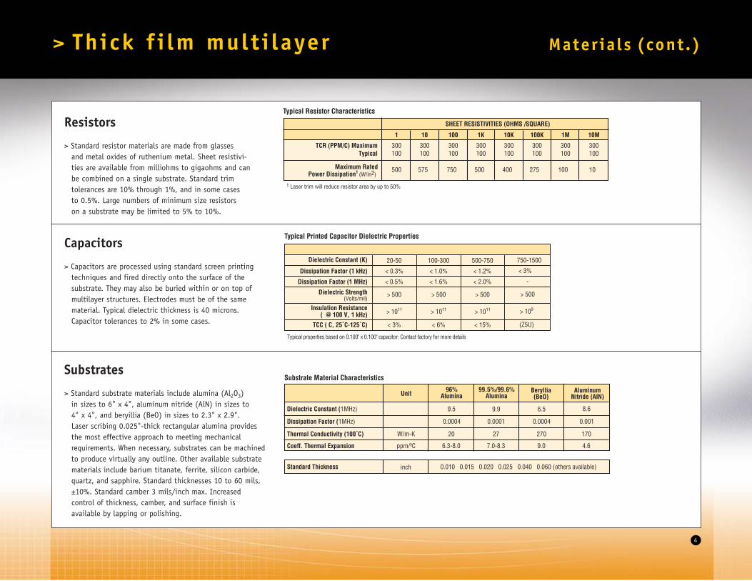
> Standard resistor materials are made from glasses and metal oxides of ruthenium metal. Sheet resistivi-ties are available from milliohms to gigaohms and can be combined on a single substrate. Standard trim tolerances are 10% through 1%, and in some cases to 0.5%. Large numbers of minimum size resistors on a substrate may be limited to 5% to 10%.
Capacitors
> Capacitors are processed using standard screen printingtechniques and fired directly onto the surface of the substrate. They may also be buried within or on top ofmultilayer structures. Electrodes must be of the same material. Typical dielectric thickness is 40 microns.Capacitor tolerances to 2% in some cases.
Substrates
> Standard substrate materials include alumina (Al2O3) in sizes to 6" x 4", aluminum nitride (AlN) in sizes to 4" x 4", and beryillia (BeO) in sizes to 2.3" x 2.9". Laser scribing 0.025"-thick rectangular alumina providesthe most effective approach to meeting mechanicalrequirements. When necessary, substrates can be machinedto produce virtually any outline. Other available substratematerials include barium titanate, ferrite, silicon carbide,quartz, and sapphire. Standard thicknesses 10 to 60 mils,±10%. Standard camber 3 mils/inch max. Increased control of thickness, camber, and surface finish is available by lapping or polishing.
1 10 100 1K 10K 100K 1M 10M
TCR (PPM/C) Maximum100 100 100 100 100 100 100 100
Maximum RatedPower Dissipation1 (W/in2)
500 575 750 500 400 10
SHEET RESISTIVITIES (OHMS /SQUARE)
Typical Resistor Characteristics
300 300 300 300 300 300 300 300
275 100
1 Laser trim will reduce resistor area by up to 50%
Typical
Dielectric Constant (K)
Dissipation Factor (1 kHz)
Dissipation Factor (1 MHz)
Dielectric Strength(Volts/mil)
Insulation Resistance( @ 100 V, 1 kHz)
TCC ( C, 25˚C-125˚C)
20-50
< 0.5%
> 500
> 1011
< 3%
100-300
< 1.6%
> 500
> 1011
< 6%
500-750
< 2.0%
> 500
> 1011
< 15%
Typical properties based on 0.100" x 0.100" capacitor: Contact factory for more details
Typical Printed Capacitor Dielectric Properties
< 0.3% < 1.0% < 1.2%
750-1500
-
> 500
> 109
(Z5U)
< 3%
Substrate Material Characteristics
Dielectric Constant (1MHz)
Dissipation Factor (1MHz)
Thermal Conductivity (100˚C)
Coeff. Thermal Expansion
Standard Thickness 0.010 0.015 0.020 0.025 0.040 0.060 (others available)inch
Unit 96%Alumina
99.5%/99.6%Alumina
Beryllia(BeO)
AluminumNitride (AIN)
W/m-K
ppm/ºC
9.5
0.0004
20
6.3-8.0
9.9
0.0001
27
7.0-8.3
6.5
0.0004
270
9.0
8.6
0.001
170
4.6
4
Mater ia ls (cont .)> Thick f i lm mult i layer

Narrow Trace& Via
Wide Trace& Via
K
G
H
D
E
F
J
Rule
Conductor WidthD
E
F
G
Minimum(mils)
Standard(mils)
Conductor Spacing
Via to Via, Isolated
Conductor Isolation inPower/Ground Plane
Conductor SpacingDifferent Materials
Minimum(mils)
Standard(mils)
H
J
Conductor to Via
5
5
7
8
10
7
7
7
10
10
15
10
7
7
10
10
12
10
10
10
12
12
15
12
Fine-Line Gold Other Golds & Silvers
EdgeView
Top
M
L
K
PN
N
Rule
Via Size(dielectric opening)K
L
M
N
Minimum(mils)
Standard(mils)
15
14
15 x 15
10 x 14
10
9
10 x 10
10 x 10
Via Fill
Conductor Over Via
Wirebond Pad Size(for 1 mil Gold Wire)
P Via to Wirebond Pad
1
5-
1 Via fill 1/2 mil smaller than via opening, all around2 Minimum size same as via size3 This spacing improves planarity of wirebond site4 Photo etchable dielectrics allow for smaller via size
2
3
4
Thick film multilayer design rules follow onthe next several pages.
> Minimum and standard feature sizes areshown. All features can be of greater sizeunless otherwise indicated.
> Feature sizes greater than the minimumimprove producibility.
Conductors & vias
5
Design features
Solder pads &gold/silver interface
R
Q S
W
V
V
U
T
XCHIP COMPONENT
Rule
Chip Pad Extension, LengthQ
Minimum(mils)
Standard(mils)
10 12
R Chip Pad Extension, Width 5 7
S Solder Pad Spacing
T Overlap Length,Dissimilar Materials
Overlap Width,Dissimilar Materials
15 -
8 12
10 12U
V Solder-Stop Overlap atGold-Silver Interface 5 7
W Glaze (solder mask)Stepback 2 5
X Glaze Width 8 15
Rules Q-S: Solder Pads 4
Rules T-X: Au-Ag Interface where required 5
4 Suggested dimensions5 Non-alloyed gold must be protected from the leaching effects of solder
> Thick f i lm mult i layer
6
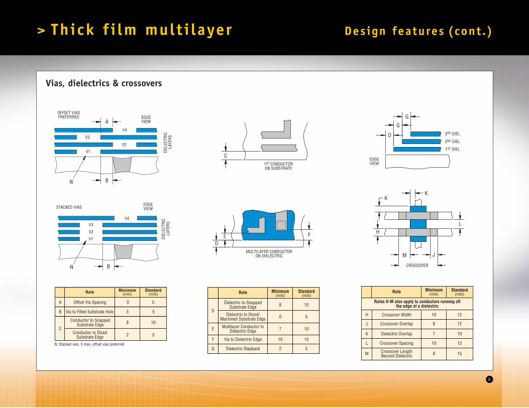
Vias, dielectrics & crossovers
OFFSET VIASPREFERRED EDGE
VIEWA
B
V4
V3
V1
V2
EDGEVIEW
V3
V2
V1
V4
B
STACKED VIAS
DIEL
ECTR
IC
LAYE
RSDI
ELEC
TRIC
LA
YERS
N
N
C1ST CONDUCTORON SUBSTRATE
MULTILAYER CONDUCTORON DIELECTRIC
FED
Rule
D
Minimum(mils)
Standard(mils)
E Multilayer Conductor toDielectric Edge
F Via to Dielectric Edge
Dielectric to SnappedSubstrate Edge
Dielectric to Diced/Machined Substrate Edge
G Dielectric Stepback
8 10
0 5
7 10
10 15
2 5
EDGEVIEW
3RD DIEL
2ND DIEL
1ST DIEL
G
G
D
KK
H
M J
L
CROSSOVER
H Crossover Width
Rule
J
Minimum(mils)
Standard(mils)
K Dielectric Overlap
L
10 12
Crossover Spacing
Crossover Overlap
M Crossover LengthBeyond Dielectric
8 12
7 10
10 12
8 15
Rules H-M also apply to conductors running offthe edge of a dielectric
Rule Minimum(mils)
Standard(mils)
A Offset Via Spacing 0 5
B Via to Filled Substrate Hole
C
Conductor to SnappedSubstrate Edge
Conductor to DicedSubstrate Edge
3 5
8 10
2 5
N: Stacked vias, 3 max.-offset vias preferred
Design features (cont .)> Thick f i lm mult i layer

7
CA
D
B
E
G
F
H
J
NOT PREFERREDACCEPTABLE
EXTRA DIELECTRIC REQD
M
K
L
Rule
Resistor LengthA
Minimum(mils)
Standard(mils)
15 30
B Resistor Width 15 30
C Resistor / TerminationOverlap
D Termination Extension(Length Direction)
Termination Extension(Width Direction)
7 10
3 5
5 8E
F Overglaze Coverage, Width 5 81
G Overglaze Coverage, Length 0 3
H Conductor to TrimmedResistor Edge 15 20
J Conductor to UntrimmedResistor Edge 10 15
Rules K-N apply to 1ST layer below resistor
K
Buried Conductor to Resistor Along Termination
15 20
L Buried Conductor toUntrimmed Resistor Edge 0 5
Buried Conductor toTrimmed Resistor Edge
M 10 15
Resistor to Resistor onCommon TerminationN 7 102
Resistor Probe PadP 10 x 10 15 x 15
Resistor Orientation Random Aligned
Resistor Loops- Loop No Loops
3
4
5
-
PREFERRED ACCEPTABLE
N
BROKEN(NO LOOP)
ALIGNED ORIENTATION RANDOM ORIENTATION
LOOP
P
1 Overglaze used where environmental stability is required2 Zero spacing allowed if both resistors use same paste3 Probe pad not covered by glaze or dielectric; located anywhere on trace; not in area reserved
for termination extension4 Orienting resistors in the same direction is especially helpful for small-geometry resistors5 Identify resistor loops in drawing notes: contact factory for details on resistors<50Ω
Design features (cont .)> Thick f i lm mult i layer
Printed capacitors
EDGEVIEW
SEALINGGLASS
TOP ELECTRODE
BOTTOM ELECTRODE
A C
B C
DIELECTRIC
Rule
Dielectric OverlapSmaller ElectrodeA
Minimum(mils)
Standard(mils)
7 10
B Larger to SmallerElectrode Overlap 2 5
C Sealing Glass/Dielectric Overlap 5 7
Bottom and top electrode can be interchanged
Printed resistors
8
Design features (cont .)> Thick f i lm mult i layer
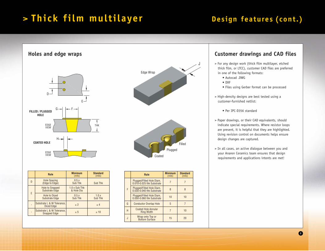
Holes and edge wraps
EDGEVIEW
G F
H
THK
D
E
EDGEVIEW
FILLED / PLUGGEDHOLE
COATED HOLE
Rule
Hole Spacing(Edge to Edge)D
Minimum(mils)
Standard(mils)
0.5 xSub Thk Sub Thk
E
Hole to SnappedSubstrate Edge
1.0 x Sub Thk& Hole Dia
Hole to DicedSubstrate Edge
0.5 xSub Thk
1.0 xSub Thk
- Substrate L & W Tolerance,Diced Edge ± 2 ± 4
± 5 ± 10- Substrate L & W Tolerance,Snapped Edge
Rule
Wrap onto Top orBottom SurfaceJ
Minimum(mils)
Standard(mils)
15 20
Plugged/Filled Hole Diam,0.010-0.025 thk Substrate
F
7 7
Plugged/Filled Hole Diam,0.030-0.040 thk Substrate 8 8
Plugged/Filled Hole Diam,0.050-0.060 thk Substrate 10 10
G Conductor Overlap Hole 5 7
H Coated Hole AnnularRing Width 7 10
Filled
Plugged
Coated
J
Edge Wrap
Customer drawings and CAD files
> For any design work (thick film multilayer, etched thick film, or LTCC), customer CAD files are preferred in one of the following formats:
• Autocad .DWG• DXF• Files using Gerber format can be processed
> High-density designs are best tested using a customer-furnished netlist:
• Per IPC-D356 standard
> Paper drawings, or their CAD equivalents, should indicate special requirements. Where resistor loops are present, it is helpful that they are highlighted.Using revision control on documents helps ensuredesign changes are captured.
> In all cases, an active dialogue between you and your Anaren Ceramics team ensures that designrequirements and applications intents are met!

9
> Lower-cost microwave c i rcuit ry
Line
Los
s (d
B/in
ch)
0.00
0.25
0.50
0.75
1.0099.6% vs. 96% Alumina - 50Ω Lines0.025" Thick
96% Alumina99.6% Alumina
4 8 12 16 20 24 28 32 36 40
FREQUENCY (GHz)
0.00
0.25
0.50
0.75
1.00Thick Film - 50Ω Line99.6% Alumina, 0.010" Thick
4 8 12 16 20 24 28 32 36 40
FREQUENCY (GHz)
Line
Los
s (d
B/in
ch)
0.00
0.25
0.50
0.75
1.00
FREQUENCY (GHz)
4 8 12 16 20 24 28 32 36 40
Line
Los
s (d
B/in
ch) THICK vs. THIN Film - 50Ω Lines
99.6% Alumina, 0.025" Thick
Thin FilmThick Film
Advanced etchingtechnology
Microwave structures can beintegrated onto your substrate
> Filters, inductors, microstrips, Lange couplers withcrossovers
> Etched thick film gold or silver conductors
> Excellent line edge definition
> An innovative combination of thin film photoimagingtechnology and advanced thick film materials produceshigh-performance, cost-effective microwave circuits.
> Thin film performance at thick film costs — up to 40% savings over thin film
Combine etched features withmultilayer features
> Capacitors, resistors, hole fill, wraps, solder- and braze-metallizations
> Alumina (96%, 99.5%, 99.6%), ferrite, aluminumnitride, Berryllium Oxide and Quartz substrates
> Standard and low-K dielectrics
And use etched thick film to achieve high-density interconnect
A ± t
B ± t
A
B
A ± t
C
ETCHED CONDUCTORS
Rule
Conductor WidthA
t
B
C
Minimum(mils)
Standard(mils)
2
±0.2
2
Ø3
1
±0.1
1.3
Ø2
Line Width Tolerance
Conductor SpacingSame Print Mask
Via Size(Photo Imaged Dielectric)

10
Overview
> Anaren Ceramics offers Low Temperature Co-fired Ceramic(LTCC) technology as an attractive solution for high-den-sity multilayer networks and high-frequency applications.Anaren Ceramics supplies the customer with a totallyintegrated solution to real-world problems by employingany and all of the following:
> Integrated components> Photolithographic technology> Passive element tuning by YAG laser> 100% continuity testing> Brazing capabilities
> Below is a pictorial representation of the LTCC manufacturing process. As shown, LTCC is a parallelprocess allowing for complex, high-density designs with high reliability and excellent mechanical and electrical properties.
> LTCC Process
11
Terms
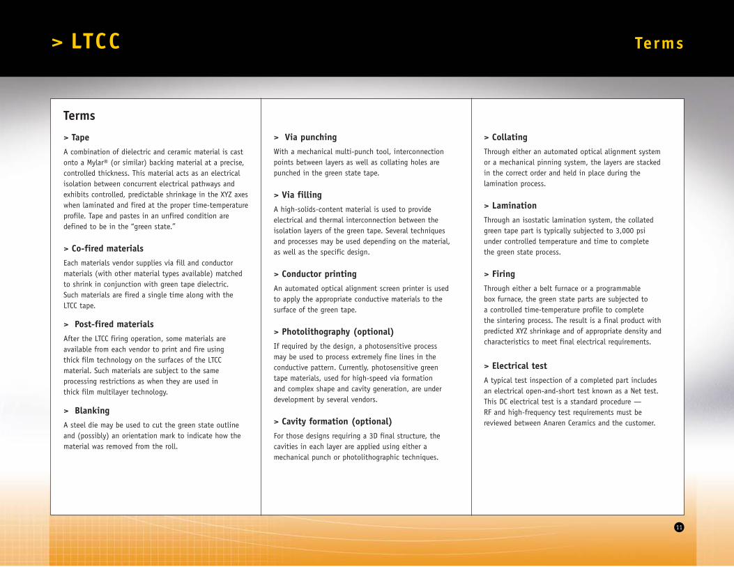
> Tape A combination of dielectric and ceramic material is castonto a Mylar® (or similar) backing material at a precise,controlled thickness. This material acts as an electricalisolation between concurrent electrical pathways andexhibits controlled, predictable shrinkage in the XYZ axeswhen laminated and fired at the proper time-temperatureprofile. Tape and pastes in an unfired condition aredefined to be in the “green state.”
> Co-fired materialsEach materials vendor supplies via fill and conductormaterials (with other material types available) matchedto shrink in conjunction with green tape dielectric. Such materials are fired a single time along with theLTCC tape.
> Post-fired materials After the LTCC firing operation, some materials are available from each vendor to print and fire using thick film technology on the surfaces of the LTCC material. Such materials are subject to the same processing restrictions as when they are used in thick film multilayer technology.
> BlankingA steel die may be used to cut the green state outlineand (possibly) an orientation mark to indicate how thematerial was removed from the roll.
> Via punching With a mechanical multi-punch tool, interconnectionpoints between layers as well as collating holes arepunched in the green state tape.
> Via fillingA high-solids-content material is used to provide electrical and thermal interconnection between the isolation layers of the green tape. Several techniques and processes may be used depending on the material, as well as the specific design.
> Conductor printing An automated optical alignment screen printer is used to apply the appropriate conductive materials to the surface of the green tape.
> Photolithography (optional) If required by the design, a photosensitive process may be used to process extremely fine lines in the conductive pattern. Currently, photosensitive green tape materials, used for high-speed via formation and complex shape and cavity generation, are underdevelopment by several vendors.
> Cavity formation (optional)For those designs requiring a 3D final structure, the cavities in each layer are applied using either a mechanical punch or photolithographic techniques.
> CollatingThrough either an automated optical alignment system or a mechanical pinning system, the layers are stacked in the correct order and held in place during the lamination process.
> Lamination Through an isostatic lamination system, the collated green tape part is typically subjected to 3,000 psi under controlled temperature and time to complete the green state process.
> FiringThrough either a belt furnace or a programmable box furnace, the green state parts are subjected to a controlled time-temperature profile to complete the sintering process. The result is a final product withpredicted XYZ shrinkage and of appropriate density andcharacteristics to meet final electrical requirements.
> Electrical testA typical test inspection of a completed part includes an electrical open-and-short test known as a Net test.This DC electrical test is a standard procedure — RF and high-frequency test requirements must bereviewed between Anaren Ceramics and the customer.
> LTCC Terms

12
Materials> Options for various materials can be found in
Tables 1 and 2. These options cover the most popular, currently available materials for tape, gold metal systems, silver metal systems, and mixed metal systems.
> Specific material choices are highly dependent upon the circuit electrical, physical, and environmental requirements, as well as the specific processing operations to be performed on the final board. Cost is also a factor that may impact the choice of specific materials used in the final design.
> Additionally, current and new vendors are continually developing materials for various applications. Final materials selection and recommendations should be the result of collaboration between the customer and the Anaren Ceramics’ engineers.
> Key features for gold metal systems, silver metal systems, and mixed metal systems are listed in Table 3 on page 14.
Table 1: Dielectric/Tape Base Material Features
943C2 45 µm943PT 95 µm943P2 135 µm943PX 210 µm
951 943 A6-M/SFired Thickness (per layer)
Loss Tangent @ 40 GHzDissipation Factor @ 1 MHzInsulation Resistance, Single Tape Thickness
DuPont
Average K @ 1MHz
Breakdown Voltage Per 25 µm Thickness Fired Density
Notes: a) 8-layer laminate structure, no metalization.
Typical Ra Surface FinishFracture Strength
TCE
Thermal Conductivity (Without Thermal Vias)
Potential Cambera
FeatureManufacturer
951C2 45 µm 951PT 95 µm951P2 135 µm951PX 210 µm
0.02400.15%
320 MPa
7.8
> 1000 VDC3.1 g/cm3
> 1012 ohms
< 10 µ-in.
3.0 W/m K
5.8 ppm/ C
< 3 µm/cm
0.00200.09%
230 MPa
7.4
> 1100 VDC3.2 g/cm3
> 1012 ohms
< 25 µ-in.
4.4 W/m K
6.0 ppm/ C
< 3 µm/cm
Ferro Coors96% Al2O3 (Ref.)
0.00200.20%
130 MPa
5.9
> 800 VDC2.5 g/cm3
> 1012 ohms
< 10 µ-in.
2.0 W/m K
7.0 ppm/ C
< 3 µm/cm
-5 95 µm-10 190 µm
0.00150.30%
400 MPa
9.5
> 2500 VDC3.6 g/cm3
> 1014 ohms
< 25 µ-in.
21.0 W/m K
7.1 ppm/ C
< 3 µm/cm
N/A
951 943 A6-M/S
Inner Layer Au
Wirebond Post-Fire Au
Solderable Au
DuPont
Wirebond Co-Fire Au
Photoimageable Au
Brazing Material (AuSn, AuGe Braze)Inner Layer Ag
Via Fill Ag
Solderable Co-Fired AgSolderable Post-Fired Ag
Process
Manufacturer
5734
5956
5742 (Al wire)5734 (Au wire)
5743 (Al wire)5715 (Au wire)5739 (Pt/Au)
6142 (Signal)6148 (Power, Gnd)
5062/5063
6141 (Ag)6138 (Pd/Ag)
5725 (Al wire)5715 (Au wire)
HF612 (Signal)HF602 (Power, Gnd)
HF502 (Au wire)
5956
HF515 (Pt/Au)
5062/5063
HF600 (Ag)HF640 (Pd/Ag)
HF615 (Pd/Ag)
Ferro
HF502
33-398
30-065 (Al wire)30-025 (Au wire)
4002
36-020 (Pt/Au)
4007
33-343 (Ag)39-005 (Pd/Ag)
33-391
30-025
Via Fill Au
Co-Fired ResistorsPost-Fired Resistors
Co-Fired Dielectric
Post-Fired Overglaze
Photoimageable Dielectric
6146 (Pd/Ag)
CF Series6135 (Pd/Ag)
7200 Series200 Ω/square
6160 (Pd/Ag)
961510K Ω/square
QQ550
87 Series3350
10-08882 Series
NCAa
5738 HF500 30-078
9615
QQ550
6050 6050
30-068 (Al wire)
NCAa
Table 2: Material Options
Note: a) NCA = Not currently available
> LTCC Mater ia ls

13
Vias
> Vias in the green tape material provide electrical and/orthermal connections between consecutive layers of thematerial (see Figure 1). The type of via used (stacked,staggered, thermal, spreading, or hermetic) is dependentupon the specific circuit requirements for electrical and thermal performance. The via selection can have a significant impact on the overall product yield, and therefore generally represents an intelligent compromise between meeting customer requirements and maximizing manufacturability.
> Standard green state via diameters are: 125 µm, 175 µm, and 250 µm. Other via diameters and/ornon-round punches can be employed but
require ordering additional tooling with a 3- to 5-weeklead time. In all cases, 250 µm is the maximum via diameter for successful via fill operations. For maximum manufacturability, via diameter should beapproximately the same as the green tape thickness.
> Standard via pitch (see Figure 2) is 3 X diameter + tapethickness. Minimum center-to-center via pitch: 1.5 Xdiameter + tape thickness. Unless otherwise specified by design, minimum distance from via center to part edge is 3 X via diameter.
> Standard capture pads for vias: via diameter + 125 µm.Minimum capture pads for vias: via diameter + 40 µm.
> Stacked and staggered vias are recommended for most applications to minimize top metal pad non-flatness — known as “via posting” — evident after the lamination process. For thermal vias use, 250 µm vias (green state, 210 µm after firing) on a 500 µm staggered grid pattern (green state, 435 µm after firing) are recommended.
> Due to the nature of via fill materials, those applica-tions requiring hermetic packages must have one intacttape layer, or offset staggered via, between a thermalvia construct and the outside package surface.
FIGURE 1: VIA DEFINITION, CROSS-SECTION
CONDUCTORTHICKNESS
DIELECTRICTHICKNESS
THERMALSPREADING
VIAS
HERMETICTHERMAL
VIAS
NON-HERMETICTHERMAL VIAS
STAGGEREDVIAS
STACKEDVIAS
CONDUCTORTO EDGE
VIA PITCH
VIA CAPTURE PAD
CONDUCTORWIDTH
RESISTOR
CONDUCTOR SPACE
GRIDDED/SOLIDGROUND PLANE
FIGURE 2: FEATURE DEFINITION, TOP VIEW
> LTCC Design features

14
Conductors
> Minimum distance from conductor to edge (see Figure 2, page 13) is 250 µm. Minimum line and spacing capability for co-fired and post-fired conductors is defined in Table 3.
> Ground and power plane capabilities are listed in Table 3. Gridding both types of features is highly recommended to improve flatness, reduce shrinkageirregularities, improve overall structural strength and integrity, and improve manufacturability.
> All gold/silver interfaces, co-fired or post-fired, must employ a transition metal to prevent Kirkendall voiding. Typically the transition metal is a palladium silver material between the silver and gold conductors.
> LTCC Design features (cont .)
Table 3: Design Guidelines Summary
Tape Layer Count
Via Diameter, 215 µm Tape
Via Capture Pad, Post-Fired
Standard Guides
Via Diameter, 95 µm Tape
Thermal Vias, 95 µm Tape
Notes: a) Typical with current tooling. Custom tooling will allow a maximum fired size of 160 x 160 mm. More complex size and shape designs can be addressed on an individual basis. b) Up to 60 layers are possible with alternative processing techniques.
Thermal Vias, 215 µm Tape
Distance, Conductor to Edge
Internal Ground/Power Plane Coverage
Minimum Tape Layer Count or Minimum Thickness
Design Feature
150 µm min. 6-7mil
250 µm ø 10 mil
180 µm min. 7-8mil
250 µm ø 10 mil
320 µm min.
100 mm x 100 mm
Grid: 40% MetalLocalized: 100%
250 µm min. 10 mil
8 Layers or 1 mm,Whichever is More
Premium Guides Photolithography Guidesc
8-20 LayersMax. Substrate Size, Fireda
Conductor Lines/Spaces
Via Capture Pad, Co-Fired Via ø + 125 µm
Via ø + 200 µm
75 µm min. 3 mil
125 µm min. 5 mil
125 µm ø 5 mil250 µm pitch 10 mil
250 µm min.
100 mm x 100 mm
Grid: 60% MetalLocalized: 100%
175 µm min.
8 Layers or 1 mm,Whichever is More
Up to 30 Layersb
Via ø + 40 µm
Via ø + 125 µm
30 µm min. 1.2 mil
180 µm ø 300 µm pitch
125 µm min. 5 mil
125 µm ø 250 µm pitch
175 µm min.
100 mm x 100 mm
Grid: 60% MetalLocalized: 100%
125 µm min.
8 Layers or 1 mm,Whichever is More
Up to 30 Layersb
Via ø + 30 µm
Via ø + 110 µm
180 µm ø300 µm pitch
Brazing
> Conductors for successful brazing to LTCC are availablefor the primary tape systems. Please refer to Table 2on page 12 for the specific material choices.
> To meet MIL Specification Visual Inspection Criteria, it is recommended that the brazing pad be 750 to 1000 µm larger than the lead or seal ring component.
> Gold-tin or gold-germanium soldering is recommended for most applications. Anaren Ceramics has soldering capability for those customers requiringa completed package.

15
Passive elements
> Inductors, resistors, and capacitors may all be inte-grated into a standard LTCC structure. Electrical characteristics are achieved through a combination of design (e.g., surface real estate, one or more layers), inherent properties of the green tape, and the material system chosen.
> Depending upon the material system, enhancementmaterials exist to locally increase the dielectric constant for some capacitor ranges. Specifics must be reviewed on a design-by-design basis.
> Buried resistors will exhibit a tolerance of +30%.Surface resistors may typically be laser trimmed usinga Nd:YAG laser to +2% to +5%. Tighter tolerancerequirements must be reviewed on a design-by-designbasis. Resistor values are limited by design and material availability, but typically run between 10 Ω and 100 kΩ for buried resistors, and 1 Ωto 100 MΩ for surface resistors. Minimum buried resistor size is 750 x 750 µm; minimum surface resistor size is 500 x 500 µm.
> Overcoat and solder-blocking materials are availableas post-fired operations.
Cavities
> Cavities are defined as openings or through-holes in the LTCC structure that are introduced into thegreen state structure prior to firing. Post-machinedoperations (CO2 laser drilling, ultrasonic milling, etc.)are not included in the recommendations below.
> Minimum distance between adjacent cavities or through-holes, or between cavity walls or though-holes and the part edge, is 2500 µm.
> Minimum cavity length and width are 2500 µm.Maximum ratio of cavity depth to minimum XY dimension is 1:1. Preferred ratio is 1:2. Minimumradius on any corner of a cavity is 500 µm.
> Cavities with floors must have a minimum floor thickness of 500 µm. Via and conductor limitationsrelated to cavity walls or cavity shelves are the same as those listed on page 13, “Vias,” paragraph 3,and page 14, “Conductors,” paragraphs 1 through 3.
> Cavities may have one or more intermediate shelves.Minimum shelf thickness is 500 µm. Minimum shelfwidth is 1200 µm.
> Maximum combined surface area of cavity opening tototal part surface area is 60%. Preferred maximumratio is 40%.
> LTCC Design features (cont .)
Electroplating, electroless plating, and etching
> As a vertically integrated facility, Anaren Ceramicsoffers electroplating (Ni/Au and Ni/Pb-Sn), and elec-troless plating (Ni/Au).
Singulation
> Primary methods for component singulation are: lasermachining and diamond saw, which may be used incombination.
> Singulations requires a minimum of 1500 µm of non-active area surrounding the final circuit. A minimumof two optical alignment features parallel to the finaledge must exist for each circuit.
> For complex shapes, CO2 machining offers routingcapability for teh LTCC substrate.
> Diamond saw dicing offers minimal dimensional devia-tion for standard, rectangular shapes.
> Anaren Ceramics employs a Nd:YAG laser trim systemfor resistive and capacitor element trimming. This equipment is also capable of active trimming or non-standard testing with the appropriate equipment.Please contact the appropriate engineering personnelwhen such trimming and testing are required.
Testing
> DC electrical testing can be achieved with either anelectrical Net test (opens and shorts) or a capacitorTAC test. It is preferred that the customer supply anASCII Netlist per IPC-D356.

16
> Design capabi l i t ies
RF/Microwave design, simulationand test capability
> Advanced RF/Microwave design, simulation and testcapability.
> Simulation tools allow accurate designs and quick turn-around time.
> 3D electro-magnetic and linear RF/MW simulation capa-bility.
> Narrow and wide-band RF/MW design capability.
> In house small signal and high power test capability.
> Thermal and Stress Simulation capability
> Thermal Simulation ensures power handling capabilityis optimized before circuit fabrication.
> Extensive life testing leads to ultra reliable parts.
3D Electro-magnectic modeling
Thermal and stress simulation
Measured and modeled insertion loss in dB
Measured and modeled return loss in dB

Style 2: Dual wrap
Common surface mount style; both terminations wrap around from resistor side to backside; solder or epoxy attach
17
> Chip resistors Style select ion
Style 1: Top contact, no wrap
Pads on resistor side only; usewith wire-bonding; backsidemetallization optional
Style 3: Single wrap
One termination wraps fromresistor side to full coverage onbackside; attach wire to theother termination; use as aterminator or to increase ther-mal contact
Listed on the following page are some of the more common chip sizes, styles, and terminations that AnarenCeramics provides. If you do not find what you’re looking for, call with your particular needs!
> Sizes as small as 20 x 20 mils (0.5 x 0.5 mm)and 12 x 24 mils (0.3 x 0.6 mm)
> Wide resistance range, from approximately 0.2 Ωto 50 GΩ. There are some limitations on size, tolerance, and TCR at the ends of these ranges.
> Tolerance to 1%, with tolerances to 0.1% available in some instances
> Anaren Ceramics is QPL listed per MIL-PRF-55342.See the QPL or call for specifics.
> Termination materials include:
• Gold for wirebonding• Platinum-gold, palladium-silver for soldering
or conductive epoxy attachment• Tin-lead plate, matte-tin, and gold plate for
soldering. These terminations consist of threelayers: a plateable silver, a solderable nickel barrierlayer, and the outer plated layer.
• Optional solder tinning. In addition to the plating options, a relatively thick printing of solder (tin-lead or gold-tin) can be added on the mounting surface only.
> Hi-rel processing is also available, adding 100% thermal shock
THE INDUSTRY’S SMALLEST WIRE-BONDABLE CHIP RESISTOR is available in two styles, 20 x 20 mils
STYLE 1: 20 X 20 mils, top contact STYLE 3: 20 X 20 mils, back contacttwo top wirebond contacts, optional backside metal
only one wirebond required, backside metal is second contact

18
> Chip resistors Order ing information
Matte Sn plate
Matte Sn plate
none T
Matte Sn plate N N N
Au
Sn-Pb plateAu plate
Pt-Au
Au
Pt-Au
Pd-Ag
Resistor Surface
none
none
none
none
Pd-Ag
Sn-Pb plateAu plate
AuAu
none
Au
Pd-AgSn-Pb plate
Pt-Au
Au plate
Pd-AgPt-Au
Back Surface
Style1
A
D
C
P
B
G
LJ
H
K
FE
Style2
G
LJ
H
K
Style3
G
LJ
H
K
FE
A metallized back surface on Style 1 chips is not connected to either resistor termination.On Style 3 chips, the back surface metallization material is the same as the wrapped resistor termination.
R 2 B 3 2 1 7 - 4 7 0 2 J 5 F 0INSPECTION
R StandardH High relM MIL-PRF-55342 C Custom
STYLE
1 Top contact2 Dual wrap3 Single wrap
BASE MATERIAL & THICKNESS
Alumina:
A 10 milB 15 milC 20 mil D 25 mil
METRIC SIZE
See table of sizes
RESISTANCE
3 digits + multiplier, except when “R” is used as a decimal5R00 5 50R0 50 1000 100 1001 1 k 1004 1 M
TOLERANCE
F 1%G 2%J 5% K 10%
M 20%N 30%R +100%, -50%S Special
TCR
3 100 ppm4 200 ppm5 300 ppm (standard)
TERMINATIONS
See table of terminations
OPTIONS
0 NoneN UntrimmedT Sn62 tinned R Gold-tin
(T, R see style selection page) Beryllia & other thicknesses available
0202
0502
0504
0302
0505
0603
0705
2010
1505
Inchsize code
0.020
0.050
0.040
0.050
0402
2512
0805
1005
1206
1010
0.030
0.050
0.075
0.200
0.080
0.060
0.100
0.150
0.125
0.250
0.100
Length(inch)
Width(inch)
Metricsize code
Length(mm)
Width(mm)
Power(W)
TA=70ºC
Voltage(V)
0505
1306
1310
0805
1313
1508
1913
5125
3813
1005
6432
2013
2513
3217
2525
0.020
0.025
0.020
0.040
0.020
0.050
0.050
0.100
0.050
0.030
0.050
0.050
0.065
0.125
0.100
0.51
1.27
1.02
1.27
0.76
1.27
1.91
5.08
2.03
1.52
2.54
3.81
3.18
6.35
2.54
0.51
0.64
0.51
1.02
0.51
1.27
1.27
2.54
1.27
0.76
1.27
1.27
1.65
3.18
2.54
0.250
0.125
0.080
0.200
0.060
0.250
0.280
1.500
0.280
0.180
0.375
0.560
0.600
2.300
0.750
30
40
32
40
24
40
60
160
60
48
80
120
100
200
80
Available termination materials and codesChip resistor sizes & specifications (use metric size for ordering)
Part numbering

19
Style P: Top contact I/O with ground wrap
Shunt attenuator withwirebond I/O pads andwrap-around grounds forconductive epoxy attach
Custom styles…
… such as this dual-shuntattenuator with wirebondI/O’s and wrap-aroundgrounds; parts can bedesigned to meet yourrequirements
10
13
16
19
1 18Frequency (GHz)
Attenuation
13 dB
0
10
20
30
40
1 18Frequency (GHz)
Return Loss
17
20
23
26
29
Frequency (GHz)
Attenuation
1 18
23 dB
0
10
20
30
40
Frequency (GHz)
Return Loss
1 18
Style A: Dual wrapI/O pads
Shunt attenuator (pi-pad) with wrap- around I/O’s and groundsfor solder attach
Anaren Ceramics’ attenuators are summarized as follows.If you do not see what you require, please do not hesi-tate to contact us to explore alternative solutions thatmay suit your particular needs!
> Characterized to 18 GHz
> Rated 0.125 W, 25 V at TA = 70ºC
> Termination materials include:
• Gold for wirebonding• Platinum-gold, palladium-silver for soldering
or conductive epoxy attachment
• Tin-lead plate, Matte-tin plate, gold plate for solder-ing. These terminations consist of three layers: aplateable silver, a solderable nickel barrier layer, andthe outer plated layer.
• Optional solder tinning. In addition to the plating options, a relatively thick printing of solder (tin-lead or gold-tin) can be added on the mounting surface only.
> Hi-rel processing is also available, adding 100% thermal shock.
0
1
2
3
4
1 18Frequency (GHz)
Attenuation
2.5 dB
0
10
20
30
40
1 18Frequency (GHz)
Return Loss
Typical Performance Data
> Chip attenuators Style select ion
20
> Chip attenuators Order ing information
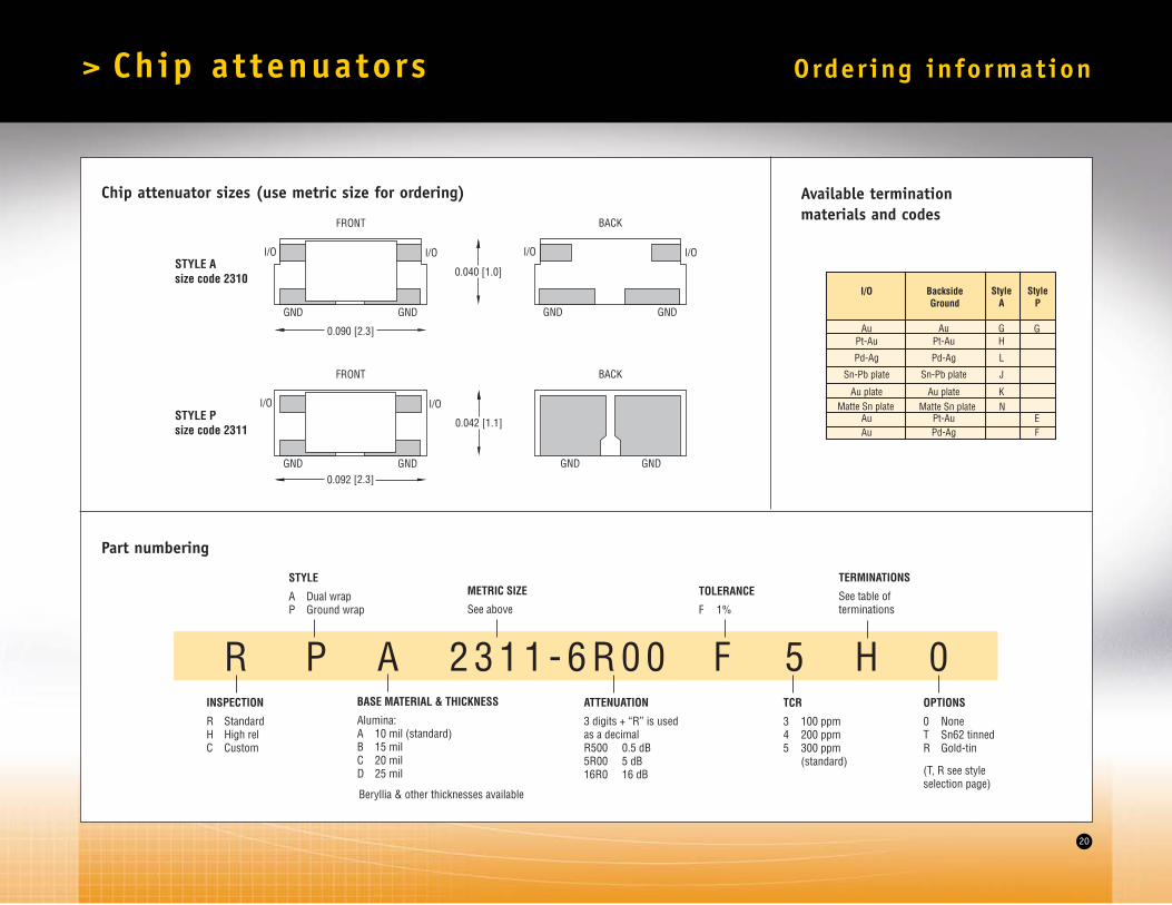
R P A 2 3 1 1 - 6 R 0 0 F 5 H 0INSPECTION
R StandardH High relC Custom
STYLE
A Dual wrapP Ground wrap
BASE MATERIAL & THICKNESS
Alumina: A 10 mil (standard)B 15 milC 20 mil D 25 mil
METRIC SIZE
See above
ATTENUATION
3 digits + “R” is used as a decimalR500 0.5 dB5R00 5 dB16R0 16 dB
TOLERANCE
F 1%
TCR
3 100 ppm4 200 ppm5 300 ppm (standard)
TERMINATIONS
See table of terminations
OPTIONS
0 NoneT Sn62 tinned R Gold-tin
(T, R see style selection page)
Beryllia & other thicknesses available
N
Au
Sn-Pb plate
Au plate
Pt-Au
AuAu
I/O
Pd-Ag
Backside Ground
StyleA
G
J
L
K
HG
StyleP
EF
Au
Sn-Pb plate
Au plate
Pt-Au
Pt-AuPd-Ag
Pd-Ag
Matte Sn plate Matte Sn plate
Available terminationmaterials and codes
Chip attenuator sizes (use metric size for ordering)
FRONT
I/O
GND GND
I/O
0.040 [1.0]
0.090 [2.3]
FRONT
I/O
GND GND
I/O
0.092 [2.3]
BACK
GND GND
BACK
I/O
GND GND
I/OSTYLE A size code 2310
STYLE P size code 2311
0.042 [1.1]
Part numbering

Anaren Ceramics, Inc.27 Northwestern Drive, Salem, NH 03079603-898-2883603-898-4273 Fax www.anaren.com
A subsidiary of Anaren, Inc.6635 Kirkville Road, East Syracuse, NY 13057315-432-8909 800-411-6591315-432-9121 Fax www.anaren.com
The Anaren CeramicsProduct & Design GuideOffering innovative precisionceramic substrate solutions:
> Thick film> LTCC> Chip components> Lower-cost microwave circuitry> Advanced etching technology
We’re ready to help!Whatever you’re thinking, we’re readywith information, design assistance, samples, quotations — anything and everything you need to develop those never-before-possible solutions. Simply call us at 603-898-2883, e-mail us at [email protected], or visit www.anaren.com.
Anaren Ceramics highlights!> Multilayer, double-sided thick film substrates
> Photo Imageable dielectrics for reduced via size and spacingin multilayers
> Lower-cost microwave circuitry, featuring advanced etching technology
> LTCC substrates up to 30 layers
> Etched line width and spacing — controlled to an order of magnitude better than traditional screen printing for lower-loss, higher-density circuits
> Alumina substrates 96%, 99.5%, and 99.6%
> Ferrite, beryllia, aluminum-nitride substrates
> Lines and spaces down to 1 mil
> Edge wraps and metallized substrate vias
> In-house plating: gold-tin, matte-tin, tin-lead, nickel
> Specific metallizations for wire bonding, soldering, or brazing
> Integrated laser-trimmed resistors
> Integrated laser marking and serialization
> Integrated capacitors, inductors, and thermistors
> Machining of substrates to any shape
> Proprietary method for creating structures with blindfeatures such as open cavities and counterbores
> Net testing
> ISO-9001:2000 registered facility
> Vertical integration: All processes from CAD toshipped product are performed in-house
> Microwave modeling, design and test capability
> Circuit layout assistance
> Extensive industry experience in materials, ceramics,and microelectronics design
> Standard and custom chip resistors and attenuators, plus QPL-listed chips per DESC MIL-PRF-55342