y8002 microprocessor technical manual - systemyde · test bench ... 4 the architecture ... the...
TRANSCRIPT
Y8002 Microprocessor Technical Manual
Systemyde International Corporation

Every effort has been made to ensure the accuracy of the information contain herein. If you find errors orinconsistencies please bring them to our attention. In all cases, however, the Verilog HDL source code forthe Y8002 design defines “proper operation”.
Copyright © 2003, 2009, 2012, Systemyde International Corporation. All rights reserved.
Notice:
“Z8000”, “Z8001”, “Z8002” and “Zilog” are registered trademarks of Zilog, Inc. All uses of these terms inthis document are to be construed as adjectives, whether or not the noun “microprocessor”, “CPU” or“device” are actually present.

1
Index
Introduction ........................................................................................................................ 3
Programming Model ........................................................................................................... 5
Addressing and Address Modes ......................................................................................... 9
Instruction Format ............................................................................................................ 13
Instruction Set .................................................................................................................. 15
External Interface and Timing ......................................................................................... 171
Interrupts and Traps ....................................................................................................... 197
Reset ............................................................................................................................... 201
Verilog HDL Source ....................................................................................................... 203
Test Bench ...................................................................................................................... 207
Appendix 1: Execution Details ....................................................................................... 213
Appendix 2: Unimplemented Features/Instructions ........................................................ 225
Appendix 3: Trapped Opcodes ........................................................................................ 229
Appendix 4: Known Timing Differences ........................................................................ 231

2

3
Chapter 1 Introduction
This book documents the operation of the Y8002 microprocessor. The Y8002 design is supplied in VerilogHDL format and can be implemented in any technology supported by a logic synthesis tool that accepts Ver-ilog HDL. The design requires roughly 15K logic gate equivalents. Included in the design package is a testbench that exercises all implemented instructions, flag settings, and representative data patterns. The testpatterns should achieve at least 95% fault coverage.
The Y8002 CPU was designed in a clean-room environment and is a clone of the Zilog Z8002 microproces-sor. Only publicly available documentation was used to create this design so there may be minor differenceswhere the public documentation is misleading or lacking. With only a couple of exceptions, the instructionexecution times are identical between the two designs. All known differences for individual instructions arelisted in the instruction description chapter as notes.
The Y8002 design, depending on the version, may not implement all of the instructions, features or operat-ing modes of the Z8000 architecture. The specific differences, for any given version of the design, are cov-ered in the various appendices.
The Z8002 CPU is one of four variants of the Z8000 architecture, introduced by Zilog in 1979. The Z8002and Z8004 support a 16-bit linear address space and are identical except that the Z8004 added support forvirtual memory. The Z8001 and Z8003 support a 23-bit segmented address and are identical except that theZ8003 added support for virtual memory. All of these devices were implemented in NMOS technology andthe Z8001 CPU and the Z8002 CPU were available for -55C to +125C operation. Manufacturing of thesedevices ceased around 1990.
This document should always be used as the final word on the operation of the Y8002 CPU, but it is usefulto refer to the Zilog documentation if the description given here is too cryptic. The Z8000 architecture isover twenty years old, so it is assumed that it is already at least somewhat familiar to the reader, but an over-view is presented here. This document will make no attempt to describe the segmented addressing mode ofthe Z8000 architecture because it is not present in the Y8002 CPU.
The Z8000 architecture includes sixteen 16-bit general-purpose registers, and uses eight distinct data typesranging from single bits to 64-bit quadruple words and byte strings. The architecture supports eight differenttypes of addressing modes. A Z8000 architecture CPU (like the Y8002) has 111 instruction types in itsinstruction set. The multiple addressing modes and data types, when coupled with the instruction types, pro-duces 447 different instructions for the Y8002 processor instruction set.
The architecture includes status signals that can be used to determine the nature of each bus transaction. Thestatus signals can be decoded and used to implement systems having multiple memory address spaces, eachspace being dedicated to a specific purpose.
The architecture includes two operating modes: system mode, and normal mode. This feature allows theoperating system functions to be easily separated from application program functions to enhance operatingsystem and application data security.

4
The architecture provides dedicated instructions for input/output operations, allowing the separation I/Ooperations from memory-related operations (the I/O space is separate from the memory space). The dedi-cated I/O instructions can only be accessed while operating in system mode. Applications running in normalmode cannot directly affect the operation of the I/O ports. This architecture does not prevent the user fromdesigning a system with memory-mapped I/O.
The architecture includes an interrupt mechanism that processes interrupts and exceptions from varioussources. These sources include a single non-maskable interrupt, a single non-vectored interrupt, up to 256vectored interrupt sources, and traps caused by the following events: execution of a privileged instructionwhile in normal mode, execution of an extended instruction, execution of the system call instruction, and asegment trap. The interrupt mechanism stores the program status, transfers program control to an interruptservice routine, and restores program status at the end of the interrupt process. The interrupt mechanism ofthe Z8000 architecture includes a means of assigning priorities to the interrupts, but this is external to theCPU itself.
The full Z8000 architecture implements a segmented memory map that allows the processor to directlyaddress six memory spaces up to 8 Megabytes (8,388,608 bytes) each. Each memory segment consists of a64K (65,536) byte block. The sixteen address lines present on the Z8000 processors are used to access theindividual locations within the memory segment while a seven-bit segment register is used to provide accessto each of the segments. As mentioned previously, the Y8002 processor does not implement the segmentedmemory scheme. It is capable of addressing six separate memory spaces, each being a maximum of 64Kbytes.
The architecture includes a refresh-control block that is designed to generate memory refresh cycles fordynamic random access memory that may be used in conjunction with the processor.
The architecture includes provisions to allow the processor to yield control of the system address/data, con-trol, and status signals to another processor in the system in response to a bus request signal. When a busrequest is granted, the processor enters the bus-disconnect state. Program execution is suspended and theCPU disconnects itself from the bus (signals are placed into a high-impedance state). When the bus requestis removed from the processor, the CPU regains control of the bus, and continues with program execution.
The architecture includes a feature known as the Extended Processing Architecture (EPA). This featureallows the instruction set of the processor to be augmented by external devices (Extended Processing Units,or EPUs) on the bus. The extended instructions are used to exploit this feature. If an extended processingunit is available, the processor will handle only the data transfer portion of the instruction, and leave execu-tion of the instruction to the EPU. If no EPU is present, the processor can handle the instruction itself usingan extended instruction trap handling software routine. The EPA bit located in the Flag and Control Word(FCW) determines how the instruction will be handled.

5
Chapter 2 Programming Model
The Z8000 architecture contains sixteen 16-bit general-purpose registers. With only a few exceptions, allgeneral-purpose registers can be used for any instruction operand. These registers allow data ranging frombytes to quadruple words. None of the general purpose registers are affected by reset.
Word registers are specified in assembly language as R0 through R15. Sixteen byte registers (RH0-RL7) canbe used as accumulators, and overlap the first eight word registers. Registers may be paired into eight doubleword registers RR0 through RR14 for 32-bit operands. Registers may also be grouped in groups of four qua-druple word registers RQ0 through RQ12 for 64-bit operands. The double word and quadruple word regis-ters are used by operations such as Multiply, Divide, and Extend Sign.
The Z8000 architecture includes two hardware stack pointers, one for each operating mode (normal and sys-tem). The system stack pointer is used in system mode, during interrupt or trap handling, and for systemcalls. The normal stack pointer is used in normal mode and only the normal stack pointer is accessible.When operating in system mode the system stack pointer is accessed as a general-purpose register and thenormal stack pointer is accessed as a special control register. Register R15 is the stack pointer.
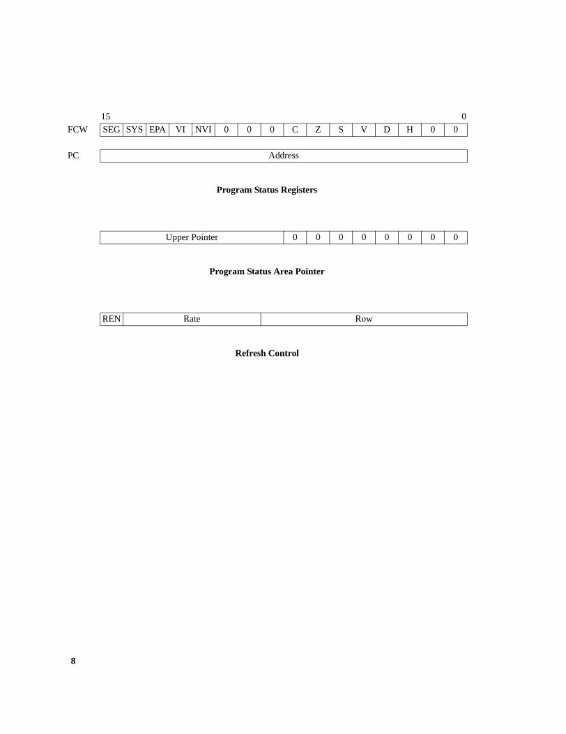
The program status reflects the current operating state of the processor. Included in the program status is theFlag and Control Word (FCW) and Program Counter (PC). The program status is automatically pushed ontothe system stack in response to an interrupt or trap. After reset, the Y8002 CPU fetches the FCW from mem-ory address 0x0002 and the PC from memory address 0x0004 before starting execution. Both of theseaddresses are in the Program address space.
The Flag and Control Word register contains both processor status bits and processor control bits. The low-order byte contains system status flags that are used by the processor instructions to control program branch-ing and looping. The high order byte contains processor control bits that are used to enable and disable theprocessor interrupt system and control certain processor operating modes.
The six processor status bits are:
• Carry (C) -- This bit indicates that a carry out of the high order bit position of a register being used as anaccumulator has occurred.
• Zero (Z) -- This bit indicates that the result of a processor operation is zero.
• Sign (S) -- This bit indicates that the result of an processor operation has produced a negative number.
• Overflow (V)-- This bit indicates that an overflow has occurred (on processor arithmetic operations) oreven parity (after processor logical operations).
• Decimal-Adjust (D) -- This bit is used in BCD arithmetic to indicate the type of instruction that wasexecuted (addition or subtraction).

6
• Half-Carry (H) --This bit is used to convert the binary result of a previous addition or subtraction ofBCD numbers into the correct decimal result.
The control bits in the high order byte of the FCW are:
• Non-Vectored Interrupt Enable (NVI) -- This bit is used to enable or disable the processor's response tointerrupts on its non-vectored interrupt input.
• Vectored Interrupt Enable (VI) -- This bit is used to enable or disable the processor's response to inter-rupts on its vectored interrupt input.
• System Mode (SYS) -- This bit determines if the processor is to operate in the system mode (High) ornormal mode (Low). The Normal/System hardware output signal of the processor is the complement ofthis bit.
• Extended Processor Architecture (EPA) -- This bit indicates the presence or absence of Extended Pro-cessing Units (EPU) in the system architecture. If EPUs are present, this bit should be set to one, and theprocessor will execute extended instructions as they are encountered. If EPUs are not present in the sys-tem and an extended instruction is fetched for execution, the processor will generate an extendedinstruction trap.
• Segmentation Mode (SEG) -- This bit is present only in a segmented Z8000 processor. When set to one,the processor is executing in segmented mode. When set to zero, the processor is executing in non-seg-mented mode. This bit is permanently set to 0 in the Y8002 processor.
The Program Counter is a sixteen bit register. All instruction fetches are 16 bits wide, so the least significantbit of the PC should always be zero. However, the hardware neither forces or checks that this is true.
The Program Status Area Pointer (PSAP) contains the address of the Program Status Area, which is a tablethat contains FCW and PC values used by the interrupt and exception handling hardware of the processor.When an interrupt or trap occurs in the processor execution cycle, the Program Status Area is where the pro-cessor obtains new values for the FCW and PC in order to process the exception. The lower byte of thePSAP is always zero. The PSAP points to an area in the Program memory address space and is cleared to allzeros by reset.
The Z8000 architecture contains hardware that can be used to automatically refresh dynamic memory in thesystem. The Refresh Control register contains a 9-bit row counter, and a six-bit rate counter, as well as anenable/disable control bit. Bit 15 of this register is cleared by reset. Modern dynamic RAMs have no need ofthis feature.

7
General Purpose Registers
15 0
R0 RH0 RL0 RR0 RQ0
R1 RH1 RL1
R2 RH2 RL2 RR2
R3 RH3 RL3
R4 RH4 RL4 RR4 RQ4
R5 RH5 RL5
R6 RH6 RL6 RR6
R7 RH7 RL7
R8 RR8 RQ8
R9
R10 RR10
R11
R12 RR12 RQ12
R13
R14 RR14
R15 System Stack Pointer
R15’ Normal Stack Pointer
8
Program Status Registers
Program Status Area Pointer
Refresh Control
15 0
FCW SEG SYS EPA VI NVI 0 0 0 C Z S V D H 0 0
PC Address
Upper Pointer 0 0 0 0 0 0 0 0
REN Rate Row

9
Chapter 3 Addressing and Address Modes
The Z8000 architecture supports separate memory and I/O address spaces, and each of these address spacescan be further subdivided if necessary. The exact address space that is being accessed is encoded on the fourstatus signals that are output buy the processor with each bus transaction. The available address spaces are:
• Program address space, with two separate status encodings to distinguish the first word of an instructionfetch from some other program memory fetch.
• Data address space, used to access data.
• Stack address space, used to access data via the stack pointer R15.
• Standard I/O address space, used for all regular I/O operations.
• Special I/O address space, which is usually reserved for I/O operations between the processor and aMemory Management Unit (MMU) or a Direct Memory Access controller (DMA).
In this architecture, each of the memory address spaces can be a maximum of 64K bytes, allowing theY8002 CPU to address 384 KB of memory. Each I/O address space is a maximum of 64K port addresses.
Each of the memory spaces can be further separated externally according to the system or normal mode.This provides the ability to design and implement operating systems that protect the system operation andinformation from being corrupted or accessed by user applications.
I/O address space is accessible only from the system mode of operation. This prevents user programs fromgaining access to system resources directly, giving the system software complete control over peripheraldevices.
The Z8000 architecture is big-endian, meaning that the most-significant data element is addressed at thelowest memory address. Bytes transferred to or from odd memory address locations (address bit 0 = 1) arealways transmitted on lines AD7-AD0 (data bit 0 on AD0). Bytes transferred to or from even memoryaddress locations (address bit 0 = 0) are always transmitted on lines AD15-AD8 (data bit 0 on AD8).
During byte writes, the CPU places the same byte on both halves of the bus. The system hardware must useAD0 to determine which half of the bus contains the actual data to be written. For byte reads, the CPU willread all 16-bits of data on the AD15-AD0 lines and automatically select the proper half of the bus that con-tains the active data.
I/O devices can use either 8-bit or 16-bit data busses for either I/O address space. The address of a peripheralwith a 16-bit wide data bus may be odd or even. Peripherals having 8-bit wide data busses connected onlines AD7-AD0 must either be addressed using odd addresses or ignore the least significant bit of theaddress and use two I/O addresses per I/O port. Normally special I/O devices connect to the upper half of thebus, and thus use even addresses.

10
Each memory address space consists of a block of 64KB of memory, with addresses being consecutivelynumbered in ascending order. The 8-bit byte is the basic addressable element in memory address space. TheZ8000 architecture supports three additional addressable data elements:
• Bits, either in bytes or words
• 16-bit words
• 32-bit long words
The type of data element being accessed depends upon the instruction being executed. The assembler mne-monics allow for addressing bit, byte, word, or long word data. Not all instructions can access all types ofdata. Addressable data elements are shown below:
A bit can be addressed by specifying an address (byte or word) and the location of the bit within the byte (7-0) or word (15-0). Bits are numbered right to left, from the least significant bit to the most significant bit.
The address of a data element longer than one byte (word, long word) is the same as that of the byte with thelowest memory address within the word or long word. This byte is the leftmost, highest-order (most signifi-cant) byte of the word or long word.
Word and long word addresses are always even-numbered. Low bytes of words are stored in odd-numberedaddresses and high bytes of words are stored in even numbered addresses. Byte data can be stored in odd oreven addresses.
Memory locations 0x0000-0x0005 in the Program memory space are reserved for the FCW and PC that arefetched after a reset. Except for this reserved memory space, there are no restrictions placed on any locationswithin the processor memory space, although the 256-byte block addressed by the PSAP is used for the Pro-gram Status information for interrupts, traps and system calls rather than program information.
The architecture supports eight data types directly, although Extended Processing Units may create andaccess new data types, such as floating point numbers. Five of the eight data types are fixed length data andthe remaining three data types have variable lengths. Each data type is supported by numerous instructionsthat operate upon it directly. The data types are as follows:
• Bit
• Signed and unsigned byte, word, double word or quadruple word binary data
bits 15 14 13 12 11 10 9 8 7 6 5 4 3 2 1 0
bytes address “n” address “n+1”
word address “n” (“n” is even)
double address “n” (“n” is even)
word address “n+2”

11
• Byte or word logical data
• Word address
• Byte of packed BCD (binary coded decimal) integer
• Dynamic-length string of byte data
• Dynamic-length of word data
• Dynamic-length of stack data
Bit data can be manipulated either in the general-purpose registers or in memory. Binary and BCD integers,and logical values may be manipulated in registers, although operands can be fetched directly from memory.Addresses can only be manipulated in registers while strings and stack data can only be manipulated inmemory.
The operands for instructions can be specified using one of eight addressing modes. For some instructionsno addressing mode is used, because the operand is implied. The majority of instructions can use any of thefive common addressing modes: register, immediate, indirect register, direct address and indexed. A fewinstructions can use the relative address mode and only load and store instructions can use base address andbase index addressing modes.
Because of the way that the addressing modes are encoded into the opcode, register R0 (and double registerRR0) cannot be used in the indirect address, index, base address or base index modes.
• Register: the contents of the register.
• Immediate: in the instruction.
• Indirect Register: the contents of the location whose address is in the register.
• Direct Address: the contents of the location whose address is in the instruction.
• Index: the contents of the location whose address is the sum of the address in the instruction plus the contents of the register.
• Relative Address: the contents of the location whose address is the sum of the contents of the Program Counter plus the displacement in the instruction.
• Base Address: the contents of the location whose address is the sum of the contents of a register plus the displacement in the instruction.
• Base Index: the contents of the location addressed by the sum of the contents of one register plus the contents of another register.

12

13
Chapter 4 Instruction Format
The format of instructions in the Z8000 architecture is quite regular. The general instruction format uses atwo bit field to select the addressing mode, a five or six bit field for the operation code (opcode), a four bitfield to select the source operand and a four bit field to select the destination operand.
In the addressing mode field the bit combination 00 usually selects either immediate data or Indirect Regis-ter addressing, the bit combination 01 selects either Direct addressing or Index addressing and the bit combi-nation 10 selects Register addressing. The choice between Immediate and Indirect Register or betweenDirect and Index is made using one of the bit combinations in bits 7-4. This is why R0 cannot be used withIndirect Register or Index addressing.
General Instruction Format (first word of instruction)
The bit combination 11 in the address mode field is used to specify the compact format for the instruction.Four of the most commonly used instructions have their own compact format.
Special Compact Instruction Format
Some infrequently used or complex instructions require two words to encode all of the information. All EPUinstructions also require at least two words.
15 14 13 12 11 10 9 8 7 6 5 4 3 2 1 0
Byte ad mode opcode 0 source or destination source or destination
Word ad mode opcode 1 source or destination source or destination
Long ad mode opcode source or destination source or destination
15 14 13 12 11 10 9 8 7 6 5 4 3 2 1 0
LDB 1 1 0 0 destination byte data
CALR 1 1 0 1 offset
JR 1 1 1 0 condition code offset
DJNZ 1 1 1 1 register W offset

14
General Instruction Format (second word of instruction)
15 14 13 12 11 10 9 8 7 6 5 4 3 2 1 0
0 0 0 0 register register condition code
0 0 0 0 register 0 0 0 0 identifier
0 0 0 0 register 0 0 0 0 0 0 0 0
EPU reserved for EPU use iteration count
EPU reserved for EPU use register reserved for EPU use iteration count

15
Chapter 5 Instruction Set
This chapter presents the assembly language syntax, addressing modes, flag settings, binary encoding, andexecution time for the Y8002 instruction set. The entire instruction set is presented in alphabetical order,without regard to whether or not a particular instruction has been implemented in a particular version of thedesign. For a list of implemented versus unimplemented instructions, refer to the appropriate Appendix.
The assembly language syntax is identical to that used by the original Zilog assembler. Different assemblerprograms may or may not use identical syntax. The syntax is presented generically at the beginning of eachinstruction, with the details presented for each addressing mode later in each entry.
The operation of each instruction is specified in a format similar to Verilog HDL for minimum ambiguity,but no descriptive text or examples are included.
The effect of the instruction on each flag is listed, with a brief description. Normally the flags are updated bythe main operation of the instruction, but for some complex instructions different flags may be affected bydifferent parts of the instruction. This is specified in the description. Where the same flag is reused during acomplex instruction a note is included at the end of the instruction description with the details.
Fields in the instruction are listed using shortcuts for common fields. These shortcuts should be self-explan-atory in most cases, but will be detailed here for completeness.
The most common fields in the instruction specify a CPU register, employing the following shortcuts:
The registers are encoded according to the following table. Note that in the case of Rdnz, Rsnz, R1nz andR2nz the “0000” case is illegal and is usually used to select a different addressing mode. The illegal casesfor RRdd, RRss and RQdd should not be used. The instructions will still execute with an illegal register
Rbdd Byte register used as a destination operand.
Rbss Byte register used as a source operand.
Rddd Word register used as a destination operand.
Rdnz Word register used in addressing the destination.
Rrrr Word register (usually specifies a counter).
Rsss Word register used as a source operand.
Rsnz Word register used in addressing the source.
R1nz Word register used in addressing the first source.
R2nz Word register used in addressing the second source.
Rxxx Word register used as an index.
RQdd Register quad used as a destination operand.
RRdd Register pair used as a destination operand.
RRss Register pair used as a source operand.

16
encoding, but the results will be scrambled in the registers because of the way the register addresses aretreated internally in the design
Immediate data is encoded in the instruction in a number of different ways, depending on the instruction.Note that the assembly language mnemonics will always use just “#data” or “#n”, independent of the actualwidth or encoding in the instruction. The following shortcuts are employed:
encoding inopcode
Rbss or RbddRddd, Rsss,
Rrrr or RxxxRsnz, Rdnz,
R1nz or R2nzRRdd, RRss RQdd
0000 RH0 R0 illegal RR0 RQ0
0001 RH1 R1 R1 illegal illegal
0010 RH2 R2 R2 RR2 illegal
0011 RH3 R3 R3 illegal illegal
0100 RH4 R4 R4 RR4 RQ4
0101 RH5 R5 R5 illegal illegal
0110 RH6 R6 R6 RR6 illegal
0111 RH7 R7 R7 illegal illegal
1000 RL0 R8 R8 RR8 RQ8
1001 RL1 R9 R9 illegal illegal
1010 RL2 R10 R10 RR10 illegal
1011 RL3 R11 R11 illegal illegal
1100 RL4 R12 R12 RR12 RQ12
1101 RL5 R13 R13 illegal illegal
1110 RL6 R14 R14 RR14 illegal
1111 RL7 R15 R15 illegal illegal
b Positive (or zero) twos-complement number used for shift left count.
-b Negative twos-complement number used for shift right count
bbb Three bit unsigned value (range 0x0 - 0x7, corresponding to 0 - 7).
bbbb Four bit unsigned value (range 0x0 - 0xF, corresponding to 0 - 15).
#data Four, eight or sixteen bit immediate data.
#data (high) Most significant word of thirty-two bit immediate data.
#data (low) Least significant word of thirty-two bit immediate data.
dddd Four bit unsigned value (range 0x0 - 0xF, corresponding to 0 - 15).
ddd_dddd Seven bit unsigned value (range 0x00 - 0x7F, corresponding to 0 - 127).
dddd_dddd Eight bit signed value (range 0x00 - 0xFF, or -127 to +128)
dddd_dddd_dddd Twelve bit signed value (range 0x000 - 0xFFF, or -2048 to +2047).
nnnn Four bit unsigned value (range 0x0 - 0xF, corresponding to 1 - 16).
ssssrccc Eight bit System Call identifier (range 0x00 - 0xFF)

17
The “cccc” field encodes one of sixteen possible flags combinations to be tested as part of the instruction, as shown in the table below. Note that some encodings have more than one possible assembly language mne-monic, and the “always true” case is implied when no other case is specified.
The remaining shortcuts should be self-explanatory. The shortcut “CZSV” is a four bit field where each bitcorresponds to the flag of the same name. The shortcut “VN” is a two bit field with each bit corresponding toone of the interrupt enable bits of the same name in the FCW.
The execution times are listed here only as a number of clock cycles. These numbers assume no wait statesand no interrupts during execution of an iterative instruction. The details of both internal and external execu-tion sequences are available in an Appendix.
ccccencoding
in opcodeFlag combination Meaning
F 0000 any Always False
LT 0001 (S ^ V) = 1 Less Than
LE 0010 (Z || (S ^ V)) = 1 Less Than or Equal
ULE 0011 (C || Z) = 1 Unsigned Less Than or Equal
OVPE
0100 V = 1Overflow
Parity Even
MI 0101 S = 1 Minus
ZEQ
0110 Z = 1ZeroEqual
CULT
0111 C = 1Carry
Unsigned Less Than
1000 any Always True
GE 1001 (S ^ V) = 0 Greater Than or Equal
GT 1010 (Z || (S ^ V)) = 0 Greater Than
UGT 1011 (!C && !Z) = 1 Unsigned Greater Than
NOVPO
1100 V = 0No OverflowParity Odd
PL 1101 S = 0 Plus
NZNE
1110 Z = 0Not ZeroNot Equal
NCUGE
1111 C = 0No Carry
Unsigned Greater Than or Equal

18
ADCAdd With Carry
ADC dst, src dst: R
ADCB src: R
Operation: dst <= dst + src + C
Flags: C: Set if arithmetic carry from result MSB; cleared otherwise.
Z: Set if result is zero; cleared otherwise.
S: Set if result is negative; cleared otherwise.
V: Set if arithmetic overflow; cleared otherwise.
D: Cleared (ADCB); Unaffected (ADC).
H: Set if arithmetic carry from bit 3; cleared otherwise (ADCB); Unaffected (ADC).
AddressingModes
Assembly Syntax Encoding Clocks
R: ADC Rd, Rs 10110101_Rsss_Rddd 5
ADCB Rbd, Rbs 10110100_Rbss_Rbdd 5

19
ADDAdd
ADD dst, src dst: R
ADDB src: R, IM, IR, DA, X
ADDL
Operation: dst <= dst + src
Flags: C: Set if arithmetic carry from MSB; cleared otherwise.
Z: Set if result is zero; cleared otherwise.
S: Set if result is negative; cleared otherwise.
V: Set if arithmetic overflow; cleared otherwise.
D: Cleared (ADDB); Unaffected (ADD).
H: Set if arithmetic carry from bit 3; cleared otherwise (ADDB); Unaffected (ADD).
AddressingModes
Assembly Syntax Encoding Clocks
R: ADD Rd, Rs 10000001_Rsss_Rddd 4
ADDB Rbd, Rbs 10000000_Rbss_Rbdd 4
ADDL RRd, RRs 10010110_RRss_RRdd 8
IM: ADD Rd, #data 00000001_0000_Rddd 7
#data
ADDB Rbd, #data 00000000_0000_Rbdd 7
#data | #data
ADDL RRd, #data 00010110_0000_RRdd 14
#data (high)
#data (low)

20
AddressingModes
Assembly Syntax Encoding Clocks
IR: ADD Rd, @Rs 00000001_Rsnz_Rddd 7
ADDB Rbd, @Rs 00000000_Rsnz_Rbdd 7
ADDL RRd, @Rs 00010110_Rsnz_RRdd 14
DA: ADD Rd, address 01000001_0000_Rddd 9
address
ADDB Rbd, address 01000000_0000_Rbdd 9
address
ADDL RRd, address 01010110_0000_RRdd 15
address
X: ADD Rd, addr(Rs) 01000001_Rsnz_Rddd 10
address
ADDB Rbd, addr(Rs) 01000000_Rsnz_Rbdd 10
address
ADDL RRd, addr(Rs) 01010110_Rsnz_RRdd 16
address

21
ANDLogical AND
AND dst, src dst: R
ANDB src: R, IM, IR, DA, X
Operation: dst <= dst & src
Flags: C: Unaffected.
Z: Set if result is zero; cleared otherwise.
S: Set if result is negative; cleared otherwise.
V: Set if result parity is even; cleared otherwise (ANDB); Unaffected (AND).
D: Unaffected.
H: Unaffected.
AddressingModes
Assembly Syntax Encoding Clocks
R: AND Rd, Rs 10000111_Rsss_Rddd 4
ANDB Rbd, Rbs 10000110_Rbss_Rbdd 4
IM: AND Rd, #data 00000111_0000_Rddd 7
#data
ANDB Rbd, #data 00000110_0000_Rbdd 7
#data | #data
IR: AND Rd, @Rs 00000111_Rsnz_Rddd 7
ANDB Rbd, @Rs 00000110_Rsnz_Rbdd 7
DA: AND Rd, address 01000111_0000_Rddd 9
address
ANDB Rbd, address 01000110_0000_Rbdd 9
address

22
AddressingModes
Assembly Syntax Encoding Clocks
X: AND Rd, addr(Rs) 01000111_Rsnz_Rddd 10
address
ANDB Rbd, addr(Rs) 01000110_Rsnz_Rbdd 10
address
23
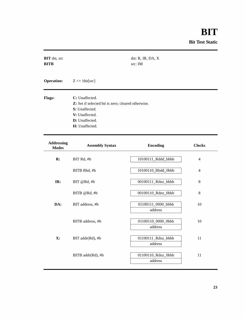
BITBit Test Static
BIT dst, src dst: R, IR, DA, X
BITB src: IM
Operation: Z <= !dst[src]
Flags: C: Unaffected.
Z: Set if selected bit is zero; cleared otherwise.
S: Unaffected.
V: Unaffected.
D: Unaffected.
H: Unaffected.
AddressingModes
Assembly Syntax Encoding Clocks
R: BIT Rd, #b 10100111_Rddd_bbbb 4
BITB Rbd, #b 10100110_Rbdd_0bbb 4
IR: BIT @Rd, #b 00100111_Rdnz_bbbb 8
BITB @Rd, #b 00100110_Rdnz_0bbb 8
DA: BIT address, #b 01100111_0000_bbbb 10
address
BITB address, #b 01100110_0000_0bbb 10
address
X: BIT addr(Rd), #b 01100111_Rdnz_bbbb 11
address
BITB addr(Rd), #b 01100110_Rdnz_0bbb 11
address

24
Notes:
1. Only bits 2-0 of the opcode are used to select the bit in the case of BITB, and bit 3 of the opcode isignored.

25
BITBit Test Dynamic
Notes:
1. The Z8000 microprocessor restricts the source register to be one of R0 - R7 for BITB. This restrictiondoes not apply to the Y8002 design. Any register may be used as the source.
2. Only bits 3-0 of the source operand are used for the bit select for BIT; only bits 2-0 of the source operandare used for the bit select for BITB.
3. Only bits 11-8 of the second word of the opcode are used. All other bits in the second word of the opcodeare ignored.
BIT dst, src dst: R
BITB src: R
Operation: Z <= !dst[src]
Flags: C: Unaffected.
Z: Set if selected bit is zero; cleared otherwise.
S: Unaffected.
V: Unaffected.
D: Unaffected.
H: Unaffected.
AddressingModes
Assembly Syntax Encoding Clocks
R: BIT Rd, Rs 00100111_0000_Rsss 10
0000_Rddd_0000_0000
BITB Rbd, Rs 00100110_0000_Rsss 10
0000_Rbdd_0000_0000

26
CALLCall
Notes:
1. The address loaded into the PC is the address of the destination operand, not the data at the destinationaddress.
2. In the case of CALL @Rd a data (or stack) memory access at the address in Rd is performed but the datais discarded.
3. Bits 3-0 of the opcode are ignored.
CALL dst dst: IR, DA, X
Operation: SP <= SP - 2
@SP <= PC
PC <= dst
Flags: C: Unaffected.
Z: Unaffected.
S: Unaffected.
V: Unaffected.
D: Unaffected.
H: Unaffected.
AddressingModes
Assembly Syntax Encoding Clocks
IR: CALL @Rd 00011111_Rdnz_0000 10
DA: CALL address 01011111_0000_0000 12
address
X: CALL address(Rd) 01011111_Rdnz_0000 13
address

27
CALRCall Relative
Notes:
1. The Zilog documentation incorrectly states that the displacement is added to the Program Counter. TheZilog Z8000 devices actually subtract the displacement from the Program Counter. The Y8002 designmatches this behavior
2. The PC used for the address calculation is the PC of the next instruction.
3. The displacement is a 12-bit twos-complement number in the range -2048 to +2047. Thus the destinationmust be in the range -4092 to +4098 from the address of the CALR instruction.
CALR dst dst: RA
Operation: SP <= SP - 2
@SP <= PC
PC <= PC - (2 x displacement)
Flags: C: Unaffected.
Z: Unaffected.
S: Unaffected.
V: Unaffected.
D: Unaffected.
H: Unaffected.
AddressingModes
Assembly Syntax Encoding Clocks
RA: CALR address 1101dddd_dddd_dddd 10

28
CLRClear
CLR dst dst: R, IR, DA, X
CLRB
Operation: dst <= 0
Flags: C: Unaffected.
Z: Unaffected.
S: Unaffected.
V: Unaffected.
D: Unaffected.
H: Unaffected.
AddressingModes
Assembly Syntax Encoding Clocks
R: CLR Rd 10001101_Rddd_1000 7
CLRB Rbd 10001100_Rbdd_1000 7
IR: CLR @Rd 00001101_Rdnz_1000 8
CLRB @Rd 00001100_Rdnz_1000 8
DA: CLR address 01001101_0000_1000 11
address
CLRB address 01001100_0000_1000 11
address
X: CLR addr(Rd) 01001101_Rdnz_1000 12
address
CLRB addr(Rd) 01001100_Rdnz_1000 12
address

29
COMComplement
COM dst dst: R, IR, DA, X
COMB
Operation: dst <= ~dst
Flags: C: Unaffected.
Z: Set if result is zero; cleared otherwise.
S: Set if result is negative; cleared otherwise.
V: Set if result parity is even; cleared otherwise (COMB); Unaffected (COM).
D: Unaffected.
H: Unaffected.
AddressingModes
Assembly Syntax Encoding Clocks
R: COM Rd 10001101_Rddd_0000 7
COMB Rbd 10001100_Rbdd_0000 7
IR: COM @Rd 00001101_Rdnz_0000 12
COMB @Rd 00001100_Rdnz_0000 12
DA: COM address 01001101_0000_0000 15
address
COMB address 01001100_0000_0000 15
address
X: COM addr(Rd) 01001101_Rdnz_0000 16
address
COMB addr(Rd) 01001100_Rdnz_0000 16
address

30
COMFLGComplement Flag
Notes:
1. The Z8000 documentation lists the H flag as undefined, when in fact it is always complemented. TheY8002 design matches this behavior.
COMFLG flags flag: C, Z, S, P, V
Operation: FCW[7:4] <= FCW[7:4] ^ inst[7:4]
Flags: C: Complemented if specified; unaffected otherwise.
Z: Complemented if specified; unaffected otherwise.
S: Complemented if specified; unaffected otherwise.
V: Complemented if specified; unaffected otherwise.
D: Unaffected.
H: Complemented.
AddressingModes
Assembly Syntax Encoding Clocks
COMFLG flags 10001101_CZSV_0101 7

31
CPCompare Register
CP dst, src dst: R
CPB src: R, IR, DA, X
CPL
Operation: dst - src
Flags: C: Set if arithmetic borrow from MSB; cleared otherwise.
Z: Set if result is zero; cleared otherwise.
S: Set if result is negative; cleared otherwise.
V: Set if arithmetic overflow; cleared otherwise.
D: Unaffected.
H: Unaffected.
AddressingModes
Assembly Syntax Encoding Clocks
R: CP Rd, Rs 10001011_Rsss_Rddd 4
CPB Rbd, Rbs 10001010_Rbss_Rbdd 4
CPL RRd, RRs 10010000_RRss_RRdd 8
IM: CP Rd, #data 00001011_0000_Rddd 7
#data
CPB Rbd, #data 00001010_0000_Rbdd 7
#data | #data
CPL RRd, #data 00010000_0000_RRdd 14
#data (high)
#data (low)

32
AddressingModes
Assembly Syntax Encoding Clocks
IR: CP Rd, @Rs 00001011_Rsnz_Rddd 7
CPB Rbd, @Rs 00001010_Rsnz_Rbdd 7
CPL RRd, @Rs 00010000_Rsnz_RRdd 14
DA: CP Rd, address 01001011_0000_Rddd 9
address
CPB Rbd, address 01001010_0000_Rbdd 9
address
CPL RRd, address 01010000_0000_RRdd 15
address
X: CP Rd, addr(Rs) 01001011_Rsnz_Rddd 10
address
CPB Rbd, addr(Rs) 01001010_Rsnz_Rbdd 10
address
CPL RRd, addr(Rs) 01010000_Rsnz_RRdd 16
address

33
CPCompare Immediate
CP dst, src dst: IR, DA, X
CPB src: IM
Operation: dst - src
Flags: C: Set if arithmetic borrow from MSB; cleared otherwise.
Z: Set if result is zero; cleared otherwise.
S: Set if result is negative; cleared otherwise.
V: Set if arithmetic overflow; cleared otherwise.
D: Unaffected.
H: Unaffected.
AddressingModes
Assembly Syntax Encoding Clocks
IR: CP @Rd, #data 00001101_Rdnz_0001 11
#data
CPB @Rd, #data 00001100_Rdnz_0001 11
#data | #data
DA: CP address, #data 01001101_0000_0001 14
address
#data
CPB address, #data 01001100_0000_0001 14
address
#data | #data
X: CP (addr)Rd, #data 01001101_Rdnz_0001 15
address
#data
CPB (addr)Rd, #data 01001100_Rdnz_0001 15
address
#data | #data

34
CPDCompare and Decrement
Notes:
1. The C, Z, S and V flags are set as usual by the compare. This flag combination is used by the cc check.The Z and V flags are subsequently set per the instruction description.
2. Because the Rd, Rs and r registers are changed by the instruction, they must be separate and non-overlap-ping.
3. Bits 15-12 of the second word of the opcode are ignored.
CPD dst, src, r, cc dst: R
CPDB src: IR
Operation: dst - src
Rs <= (Word) ? Rs - 2 : Rs - 1
r <= r - 1
Flags: C: Set if arithmetic borrow from MSB for compare; cleared otherwise.
Z: Set if flags match cc after the last compare; cleared otherwise.
S: Set if result is negative for compare; cleared otherwise.
V: Set if r is zero after the decrement; cleared otherwise.
D: Unaffected.
H: Unaffected.
AddressingModes
Assembly Syntax Encoding Clocks
IR: CPD Rd, @Rs, r, cc 10111011_Rsnz_1000 20
0000_Rrrr_Rddd_cccc
CPDB Rd, @Rs, r, cc 10111010_Rsnz_1000 20
0000_Rrrr_Rddd_cccc

35
CPDRCompare, Decrement and Repeat
Notes:
1. The C, Z, S and V flags are set as usual by the compare. This flag combination is used by the cc check.The Z and V flags are subsequently set per the instruction description.
2. Because the Rd, Rs and r registers are changed by the instruction, they must be separate and non-overlap-ping.
3. Bits 15-12 of the second word of the opcode are ignored.
4. This instruction samples interrupts during each iteration. If an interrupt is pending, the instruction isstopped and the interrupt accepted. The PC saved during the interrupt acknowledge cycle in this case is thePC of the running instruction, allowing the instruction to restart after the interrupt has been serviced.
CPDR dst, src, r, cc dst: R
CPDRB src: IR
Operation: dst - src
Rs <= (Word) ? Rs - 2 : Rs - 1
r <= r - 1
repeat until cc is true or r = 0
Flags: C: Set if arithmetic borrow from MSB for the last compare; cleared otherwise.
Z: Set if flags match cc after the last compare; cleared otherwise.
S: Set if result is negative for the last compare; cleared otherwise.
V: Set if r is zero after the decrement; cleared otherwise.
D: Unaffected.
H: Unaffected.
AddressingModes
Assembly Syntax Encoding Clocks
IR: CPDR Rd, @Rs, r, cc 10111011_Rsnz_1100 11 + 9n
0000_Rrrr_Rddd_cccc
CPDRB Rd, @Rs, r, cc 10111010_Rsnz_1100 11 + 9n
0000_Rrrr_Rddd_cccc

36
CPICompare and Increment
Notes:
1. The C, Z, S and V flags are set as usual by the compare. This flag combination is used by the cc check.The Z and V flags are subsequently set per the instruction description.
2. Because the Rd, Rs and r registers are changed by the instruction, they must be separate and non-overlap-ping.
3. Bits 15-12 of the second word of the opcode are ignored.
CPI dst, src, r, cc dst: R
CPIB src: IR
Operation: dst - src
Rs <= (Word) ? Rs + 2 : Rs + 1
r <= r - 1
Flags: C: Set if arithmetic borrow from MSB for the last compare; cleared otherwise.
Z: Set if flags match cc after the last compare; cleared otherwise.
S: Set if result is negative for the last compare; cleared otherwise.
V: Set if r is zero after the decrement; cleared otherwise.
D: Unaffected.
H: Unaffected.
AddressingModes
Assembly Syntax Encoding Clocks
IR: CPI Rd, @Rs, r, cc 10111011_Rsnz_0000 20
0000_Rrrr_Rddd_cccc
CPIB Rd, @Rs, r, cc 10111010_Rsnz_0000 20
0000_Rrrr_Rddd_cccc

37
CPIRCompare, Increment and Repeat
Notes:
1. The C, Z, S and V flags are set as usual by the compare. This flag combination is used by the cc check.The Z and V flags are subsequently set per the instruction description.
2. Because the Rd, Rs and r registers are changed by the instruction, they must be separate and non-overlap-ping.
3. Bits 15-12 of the second word of the opcode are ignored.
4. This instruction samples interrupts during each iteration. If an interrupt is pending, the instruction isstopped and the interrupt accepted. The PC saved during the interrupt acknowledge cycle in this case is thePC of the running instruction, allowing the instruction to restart after the interrupt has been serviced.
CPIR dst, src, r, cc dst: R
CPIRB src: IR
Operation: dst - src
Rs <= (Word) ? Rs + 2 : Rs + 1
r <= r - 1
repeat until cc is true or r = 0
Flags: C: Set if arithmetic borrow from MSB for the last compare; cleared otherwise.
Z: Set if flags match cc after the last compare; cleared otherwise.
S: Set if result is negative for the last compare; cleared otherwise.
V: Set if r is zero after the decrement; cleared otherwise.
D: Unaffected.
H: Unaffected.
AddressingModes
Assembly Syntax Encoding Clocks
IR: CPIR Rd, @Rs, r, cc 10111011_Rsnz_0100 11 + 9n
0000_Rrrr_Rddd_cccc
CPIRB Rd, @Rs, r, cc 10111010_Rsnz_0100 11 + 9n
0000_Rrrr_Rddd_cccc

38
CPSDCompare String and Increment
Notes:
1. The C, Z, S and V flags are set as usual by the compare. This flag combination is used by the cc check.The Z and V flags are subsequently set per the instruction description.
2. Because the Rd, Rs and r registers are changed by the instruction, they must be separate and non-overlap-ping.
3. Bits 15-12 of the second word of the opcode are ignored.
CPSD dst, src, r, cc dst: IR
CPSDB src: IR
Operation: dst - src
Rs <= (Word) ? Rs - 2 : Rs - 1
Rd <= (Word) ? Rd - 2 : Rd - 1
r <= r - 1
Flags: C: Set if arithmetic borrow from MSB for the last compare; cleared otherwise.
Z: Set if flags match cc after the last compare; cleared otherwise.
S: Set if result is negative for the last compare; cleared otherwise.
V: Set if r is zero after the decrement; cleared otherwise.
D: Unaffected.
H: Unaffected.
AddressingModes
Assembly Syntax Encoding Clocks
IR: CPSD @Rd, @Rs, r, cc 10111011_Rsnz_1010 25
0000_Rrrr_Rdnz_cccc
CPSDB @Rd, @Rs, r, cc 10111010_Rsnz_1010 25
0000_Rrrr_Rdnz_cccc

39
CPSDRCompare String, Decrement and Repeat
Notes:
1. The C, Z, S and V flags are set as usual by the compare. This flag combination is used by the cc check.The Z and V flags are subsequently set per the instruction description.
2. Because the Rd, Rs and r registers are changed by the instruction, they must be separate and non-overlap-ping.
3. Bits 15-12 of the second word of the opcode are ignored.
CPSDR dst, src, r, cc dst: IR
CPSDRB src: IR
Operation: dst - src
Rs <= (Word) ? Rs - 2 : Rs - 1
Rd <= (Word) ? Rd - 2 : Rd - 1
r <= r - 1
repeat until cc is true or r = 0
Flags: C: Set if arithmetic borrow from MSB for the last compare; cleared otherwise.
Z: Set if flags match cc after the last compare; cleared otherwise.
S: Set if result is negative for the last compare; cleared otherwise.
V: Set if r is zero after the decrement; cleared otherwise.
D: Unaffected.
H: Unaffected.
AddressingModes
Assembly Syntax Encoding Clocks
IR: CPSDR @Rd, @Rs, r, cc 10111011_Rsnz_1110 11 + 14n
0000_Rrrr_Rdnz_cccc
CPSDRB @Rd, @Rs, r, cc 10111010_Rsnz_1110 11 + 14n
0000_Rrrr_Rdnz_cccc

40
Notes (continued):
4. This instruction samples interrupts during each iteration. If an interrupt is pending, the instruction isstopped and the interrupt accepted. The PC saved during the interrupt acknowledge cycle in this case is thePC of the running instruction, allowing the instruction to restart after the interrupt has been serviced.

41
CPSICompare String and Increment
Notes:
1. The C, Z, S and V flags are set as usual by the compare. This flag combination is used by the cc check.The Z and V flags are subsequently set per the instruction description.
2. Because the Rd, Rs and r registers are changed by the instruction, they must be separate and non-overlap-ping.
3. Bits 15-12 of the second word of the opcode are ignored.
CPSI dst, src, r, cc dst: IR
CPSIB src: IR
Operation: dst - src
Rs <= (Word) ? Rs + 2 : Rs + 1
Rd <= (Word) ? Rd + 2 : Rd + 1
r <= r - 1
Flags: C: Set if arithmetic borrow from MSB for the last compare; cleared otherwise.
Z: Set if flags match cc after the last compare; cleared otherwise.
S: Set if result is negative for the last compare; cleared otherwise.
V: Set if r is zero after the decrement; cleared otherwise.
D: Unaffected.
H: Unaffected.
AddressingModes
Assembly Syntax Encoding Clocks
IR: CPSI @Rd, @Rs, r, cc 10111011_Rsnz_0010 25
0000_Rrrr_Rdnz_cccc
CPSIB @Rd, @Rs, r, cc 10111010_Rsnz_0010 25
0000_Rrrr_Rdnz_cccc

42
CPSIRCompare String, Increment and Repeat
Notes:
1. The C, Z, S and V flags are set as usual by the compare. This flag combination is used by the cc check.The Z and V flags are subsequently set per the instruction description.
2. Because the Rd, Rs and r registers are changed by the instruction, they must be separate and non-overlap-ping.
3. Bits 15-12 of the second word of the opcode are ignored.
CPSIR dst, src, r, cc dst: IR
CPSIRB src: IR
Operation: dst - src
Rs <= (Word) ? Rs + 2 : Rs + 1
Rd <= (Word) ? Rd + 2 : Rd + 1
r <= r - 1
repeat until cc is true or r = 0
Flags: C: Set if arithmetic borrow from MSB for the last compare; cleared otherwise.
Z: Set if flags match cc after the last compare; cleared otherwise.
S: Set if result is negative for the last compare; cleared otherwise.
V: Set if r is zero after the decrement; cleared otherwise.
D: Unaffected.
H: Unaffected.
AddressingModes
Assembly Syntax Encoding Clocks
IR: CPSIR @Rd, @Rs, r, cc 10111011_Rsnz_0110 11 + 14n
0000_Rrrr_Rdnz_cccc
CPSIRB @Rd, @Rs, r, cc 10111010_Rsnz_0110 11 + 14n
0000_Rrrr_Rdnz_cccc

43
Notes (continued):
4. This instruction samples interrupts during each iteration. If an interrupt is pending, the instruction isstopped and the interrupt accepted. The PC saved during the interrupt acknowledge cycle in this case is thePC of the running instruction, allowing the instruction to restart after the interrupt has been serviced.

44
DABDecimal Adjust
Notes:
1. This instruction should only be executed on the result of an ADDB, ADCB, SUBB, or SBCB instruction,and serves to convert the binary result into a BCD number.
2. Bits 3-0 of the opcode are ignored.
3. Note that the sign flag is not really meaningful for a BCD number.
4. The byte and flags are modified according to the table below:
DAB dst dst: R
Operation: dst <= dst + da_value
Flags: C: Set or cleared according to the table in the notes.
Z: Set if result is zero; cleared otherwise.
S: Set if result is negative; cleared otherwise.
V: Unaffected.
D: Unaffected.
H: Unaffected.
AddressingModes
Assembly Syntax Encoding Clocks
R: DAB Rbd 10110000_Rbdd_0000 5

45
Notes (continued):
InstructionC before
DABdst[7:4]
before DABH before
DABdst[3:0]
before DABNumber
added to dstC afterDAB
0 0-9 0 0-9 00 0
0 0-8 0 A-F 06 0
0 0-9 1 0-3 06 0
ADDB or ADCB 0 A-F 0 0-9 60 1
0 9-F 0 A-F 66 1
0 A-F 1 0-3 66 1
1 0-2 0 0-9 60 1
1 0-2 0 A-F 66 1
1 0-3 1 0-3 66 1
0 0-9 0 0-9 00 0
SUBB or SBCB 0 0-8 1 6-F FA 0
1 7-F 0 0-9 A0 1
1 6-F 1 6-F 9A 1

46
DECDecrement
DEC dst, src dst: R, IR, DA, X
DECB src: IM
Operation: dst <= dst - src (src = 1 to 16, encoded in opcode)
Flags: C: Unaffected.
Z: Set if result is zero; cleared otherwise.
S: Set if result is negative; cleared otherwise.
V: Set if arithmetic overflow; cleared otherwise.
D: Unaffected.
H: Unaffected.
AddressingModes
Assembly Syntax Encoding Clocks
R: DEC Rd, #n 10101011_Rddd_nnnn 4
DECB Rbd, #n 10101010_Rbdd_nnnn 4
IR: DEC @Rd, #n 00101011_Rdnz_nnnn 11
DECB @Rd, #n 00101010_Rdnz_nnnn 11
DA: DEC address, #n 01101011_0000_nnnn 13
address
DECB address, #n 01101010_0000_nnnn 13
address
X: DEC addr(Rd), #n 01101011_Rdnz_nnnn 14
address
DECB addr(Rd), #n 01101010_Rdnz_nnnn 14
address

47
DIDisable Interrupt
Notes:
1. The interrupt enable bits are updated before the instruction completes, so an interrupt that is assertedwhile being disabled by this instruction will not be accepted.
DI int int: VI, NVI
Operation: FCW[12:11] <= FCW[12:11] & inst[1:0]
Flags: C: Unaffected.
Z: Unaffected.
S: Unaffected.
V: Unaffected.
D: Unaffected.
H: Unaffected.
AddressingModes
Assembly Syntax Encoding Clocks
DI int 01111100_0000_00VN 7

48
DIVDivide
DIV dst, src dst: R
DIVL src: R, IM, IR, DA, X
Operation: Word: dst[31:0] / src[15:0]
dst[31:16] <= remainder
dst[15:0] <= quotient
Long: dst[63:0] / src[31:0]
dst[63:32] <= remainder
dst[31:0] <= quotient
Flags: C: See tables below.
Z: Set if the quotient or divisor is zero; cleared otherwise.
S: See tables below.
V: See tables below.
D: Unaffected.
H: Unaffected.
AddressingModes
Assembly Syntax Encoding Clocks
R: DIV RRd, Rs 10011011_Rsss_RRdd 6 + div
DIVL RQd, RRs 10011010_RRss_RQdd 6 + divl
IM: DIV RRd, #data 00011011_0000_RRdd 8 + div
#data
DIVL RQd, #data 00011010_0000_RQdd 11 + div
#data (high)
#data (low)
IR: DIV RRd, @Rs 00011011_Rsnz_RRdd 8 + div
DIVL RQd, @Rs 00011010_Rsnz_RQdd 11 + divl

49
Notes:
1. The Zilog documentation incorrectly describes the condition used to detect overflow for a negative quo-tient. The Zilog documentation specifies that for DIV a quotient less than -(2^16) is an overflow, but Z8000devices actually signal overflow if the quotient is less than -(2^16 - 1). In the case of DIVL the documenta-tion specifies that a quotient less than -(2^32) is an overflow, but Z8000 devices actually signal overflow ifthe quotient is less than -(2^32 - 1). The Y8002 design matches the behavior of the Zilog devices.
2. In the case of overflow, the destination register(s) and S flag are undefined. The Y8002 design does notattempt to match the Z8000 microprocessor’s undefined value for this case, and the Y8002 design alwaysclears the S flag in this case.
3. All four numbers (divisor, divider, quotient and remainder) are signed twos-complement numbers. Theremainder will always have the same sign as the divisor.
4. The quotient can be a 17-bit number for DIV and a 33-bit number for DIVL. The S flag is the MSB of thequotient in this case, and can be used to extend the quotient to a full 32 or 64 bits in software. The other flagsindicate whether the S flag is actually needed to represent the number correctly.
5. The execution time and different flag cases for DIV are shown in the table below:
AddressingModes
Assembly Syntax Encoding Clocks
DA: DIV RRd, address 01011011_0000_RRdd 10 + div
address
DIVL RQd, address 01011010_0000_RQdd 13 + divl
address
X: DIV RRd, addr(Rs) 01011011_Rsnz_RRdd 11 + div
address
DIVL RQd, addr(Rs) 01011010_Rsnz_RQdd 14 + divl
address
DIV case C Z S V div cycles
1. Quotient is a 16-bit twos-complement number. 0 zero sign 0 86
2. Divisor is zero. The destination register is unchanged in this case.
0 1 0 1 5
3. Quotient is too large to represent in 17 bits. The destination reg-ister is undefined in this case.
0 0 0 1 16
4. Quotient is a 17-bit twos-complement number. 1 0 sign 1 86

50
Notes (continued):
6. The execution time and different flag cases for DIVL are shown in the table below:
7. Because the Rs (or RRs) and RRd (or RQd) are used to store intermediate results, they must be separateand non-overlapping.
DIVL case C Z S V divl cycles
1. Quotient is a 32-bit twos-complement number. 0 zero sign 0 494
2. Divisor is zero. The destination register is unchanged in this case.
0 1 0 1 8
3. Quotient is too large to represent in 33 bits. The destination reg-ister is undefined in this case.
0 0 0 1 30
4. Quotient is a 33-bit twos-complement number. 1 0 sign 1 494

51
DJNZDecrement and Jump if Not Zero
Notes:
1. The PC used for the address calculation is the PC of the next instruction.
2. The displacement is a 7-bit unsigned number in the range 0 to 127. Thus the destination must be in therange -252 to +2 from the address of the DJNZ (or DBJNZ) instruction.
DJNZ R,dst dst: RA
DBJNZ
Operation: R <= R - 1
if R != 0 the PC <= PC - (2 x displacement)
Flags: C: Unaffected.
Z: Unaffected.
S: Unaffected.
V: Unaffected.
D: Unaffected.
H: Unaffected.
AddressingModes
Assembly Syntax Encoding Clocks
RA: DJNZ R, address 1111Rrrr_1ddd_dddd 11
DBJNZ Rb, address 1111Rrrr_0ddd_dddd 11

52
EIEnable Interrupt
Notes:
1. The interrupt enable bits are updated before the instruction completes, so an interrupt that is assertedwhile being enabled by this instruction will be accepted.
EI int int: VI, NVI
Operation: FCW[12:11] <= FCW[12:11] | ~inst[1:0]
Flags: C: Unaffected.
Z: Unaffected.
S: Unaffected.
V: Unaffected.
D: Unaffected.
H: Unaffected.
AddressingModes
Assembly Syntax Encoding Clocks
EI int 01111100_0000_01VN 7
53
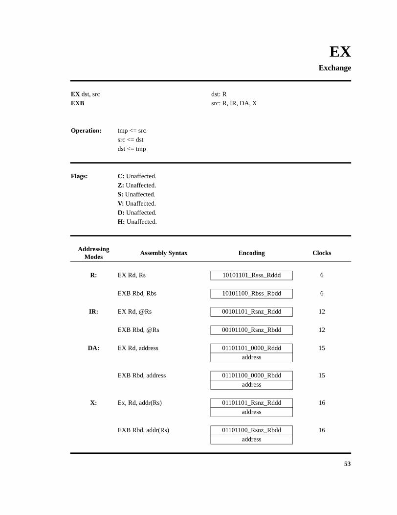
EXExchange
EX dst, src dst: R
EXB src: R, IR, DA, X
Operation: tmp <= src
src <= dst
dst <= tmp
Flags: C: Unaffected.
Z: Unaffected.
S: Unaffected.
V: Unaffected.
D: Unaffected.
H: Unaffected.
AddressingModes
Assembly Syntax Encoding Clocks
R: EX Rd, Rs 10101101_Rsss_Rddd 6
EXB Rbd, Rbs 10101100_Rbss_Rbdd 6
IR: EX Rd, @Rs 00101101_Rsnz_Rddd 12
EXB Rbd, @Rs 00101100_Rsnz_Rbdd 12
DA: EX Rd, address 01101101_0000_Rddd 15
address
EXB Rbd, address 01101100_0000_Rbdd 15
address
X: Ex, Rd, addr(Rs) 01101101_Rsnz_Rddd 16
address
EXB Rbd, addr(Rs) 01101100_Rsnz_Rbdd 16
address

54
EXTSExtend Sign
EXTSB dst dst: R
EXTSEXTSL
Operation: Byte: dst[15:8] <= (dst[7]) ? 0xFF : 0x00
Word: dst[31:16] <= (dst[15]) ? 0xFFFF : 0x0000
Long: dst[63:32] <= (dst[31]) ? 0xFFFFFFFF : 0x00000000
Flags: C: Unaffected.
Z: Unaffected.
S: Unaffected.
V: Unaffected.
D: Unaffected.
H: Unaffected.
AddressingModes
Assembly Syntax Encoding Clocks
R: EXTSB Rd 10110001_Rddd_0000 11
EXTS RRd 10110001_RRdd_1010 11
EXTSL RQd 10110001_RQdd_0111 11

55
HALTHalt
Notes:
1. Interrupts are sampled once during the initial eight-clock sequence and once during every three-clockinternal operation cycle.
2. If an interrupt is active at the time of the first sample, the instruction executes in eight clock cycles. If aninterrupt is sampled during an internal operation cycle, a subsequent internal operation cycle is performedbefore starting the interrupt acknowledge cycle.
HALT
Operation: Halt and wait for interrupt
Flags: C: Unaffected.
Z: Unaffected.
S: Unaffected.
V: Unaffected.
D: Unaffected.
H: Unaffected.
AddressingModes
Assembly Syntax Encoding Clocks
HALT 01111010_0000_0000 8 + 3n

56
(S)IN(Special) Input
IN dst, src dst: R
INB src: IR, DA
SIN dst, src dst: R
SINB dst, src src: DA
Operation: dst <= src
Flags: C: Unaffected.
Z: Unaffected.
S: Unaffected.
V: Unaffected.
D: Unaffected.
H: Unaffected.
AddressingModes
Assembly Syntax Encoding Clocks
R: IN Rd, @Rs 00111101_Rsnz_Rddd 10
INB Rbd, @Rs 00111100_Rsnz_Rbdd 10
DA: IN Rd, port 00111011_Rddd_0100 12
port
SIN Rd, port 00111011_Rddd_0101 12
port
INB Rbd, port 00111010_Rbdd_0100 12
port
SINB Rbd, port 00111010_Rbdd_0101 12
port

57
Notes:
1. Data is read from the I/O or Special I/O address space. Only the status code is different between IN andSIN.
2. I/O reads always have one automatic WAIT state. This is included in the Cycles number above.

58
INCIncrement
INC dst, src dst: R, IR, DA, X
INCB src: IM
Operation: dst <= dst + src (src = 1 to 16, encoded in opcode)
Flags: C: Unaffected.
Z: Set if result is zero; cleared otherwise.
S: Set if result is negative; cleared otherwise.
V: Set if arithmetic overflow; cleared otherwise.
D: Unaffected.
H: Unaffected.
AddressingModes
Assembly Syntax Encoding Clocks
R: INC Rd, #n 10101001_Rddd_nnnn 4
INCB Rbd, #n 10101000_Rbdd_nnnn 4
IR: INC @Rd, #n 00101001_Rdnz_nnnn 11
INCB @Rd, #n 00101000_Rdnz_nnnn 11
DA: INC address, #n 01101001_0000_nnnn 13
address
INCB address, #n 01101000_0000_nnnn 13
address
X: INC addr(Rd), #n 01101001_Rdnz_nnnn 14
address
INCB addr(Rd), #n 01101000_Rdnz_nnnn 14
address

59
(S)IND(Special) Input and Decrement
Notes:
1. The Z8000 documentation lists the Z flag as undefined. In the Y8002 design this flag is unaffected.
IND dst, src, r, cc dst: IR
INDB src: IR
SINDSINDB
Operation: dst <= src
Rd <= (Word) ? Rd - 2 : Rd - 1
r <= r - 1
Flags: C: Unaffected.
Z: Unaffected.
S: Unaffected.
V: Set if r is zero after the decrement; cleared otherwise.
D: Unaffected.
H: Unaffected.
AddressingModes
Assembly Syntax Encoding Clocks
IR: IND @Rd, @Rs, r 00111011_Rsnz_1000 21
0000_Rrrr_Rdnz_1000
SIND @Rd, @Rs, r 00111010_Rsnz_1001 21
0000_Rrrr_Rdnz_1000
INDB @Rd, @Rs, r 00111011_Rsnz_1000 21
0000_Rrrr_Rdnz_1000
SINDB @Rd, @Rs, r 00111010_Rsnz_1001 21
0000_Rrrr_Rdnz_1000

60
Notes (continued):
2. Data is read from the I/O or Special I/O address space. Only the status code is different between IND andSIND.
3. Because the Rd, Rs and r registers are changed by the instruction, they must be separate and non-overlap-ping.
4. Bits 15-12 of the second word of the opcode are ignored.
5. Bits 3-0 of the second word of the opcode are actually a condition code. The result of this condition codecheck is ORed with the r = 0 check to determine if the instruction is complete. The bit combination 1000 isthe encoding for “True”, making this a non-repeating instruction.

61
(S)INDR(Special) Input, Decrement and Repeat
Notes:
1. The Z8000 documentation lists the Z flag as undefined. In the Y8002 design this flag is unaffected.
INDR dst, src, r, cc dst: IR
INDRB src: IR
SINDRSINDRB
Operation: dst <= src
Rd <= (Word) ? Rd - 2 : Rd - 1
r <= r - 1
repeat until r = 0
Flags: C: Unaffected.
Z: Unaffected.
S: Unaffected.
V: Set if r is zero after the decrement; cleared otherwise.
D: Unaffected.
H: Unaffected.
AddressingModes
Assembly Syntax Encoding Clocks
IR: INDR @Rd, @Rs, r 00111011_Rsnz_1000 11 + 10n
0000_Rrrr_Rdnz_0000
SINDR @Rd, @Rs, r 00111010_Rsnz_1001 11 + 10n
0000_Rrrr_Rdnz_0000
INDRB @Rd, @Rs, r 00111011_Rsnz_1000 11 + 10n
0000_Rrrr_Rdnz_0000
SINDR @Rd, @Rs, r 00111010_Rsnz_1001 11 + 10n
0000_Rrrr_Rdnz_0000

62
Notes (continued):
2. Data is read from the I/O or Special I/O address space. Only the status code is different between IND andSIND.
3. Because the Rd, Rs and r registers are changed by the instruction, they must be separate and non-overlap-ping.
4. Bits 15-12 of the second word of the opcode are ignored.
5. Bits 3-0 of the second word of the opcode are actually a condition code. The result of this condition codecheck is ORed with the r = 0 check to determine if the instruction is complete. The bit combination 0000 isthe encoding for “False”, making this a repeating instruction.
6. This instruction samples interrupts during each iteration. If an interrupt is pending, the instruction isstopped and the interrupt accepted. The PC saved during the interrupt acknowledge cycle in this case is thePC of the running instruction, allowing the instruction to restart after the interrupt has been serviced.

63
(S)INI(Special) Input and Increment
Notes:
1. The Z8000 documentation lists the Z flag as undefined. In the Y8002 design this flag is unaffected.
INI dst, src, r, cc dst: IR
INIB src: IR
SINISINIB
Operation: dst <= src
Rd <= (word) ? Rd + 2 : Rd + 1
r <= r - 1
Flags: C: Unaffected.
Z: Unaffected.
S: Unaffected.
V: Set if r is zero after the decrement; cleared otherwise.
D: Unaffected.
H: Unaffected.
AddressingModes
Assembly Syntax Encoding Clocks
IR: INI @Rd, @Rs, r 00111011_Rsnz_0000 21
0000_Rrrr_Rdnz_1000
SINI @Rd, @Rs, r 00111010_Rsnz_0001 21
0000_Rrrr_Rdnz_1000
INIB @Rd, @Rs, r 00111011_Rsnz_0000 21
0000_Rrrr_Rdnz_1000
SINIB @Rd, @Rs, r 00111010_Rsnz_0001 21
0000_Rrrr_Rdnz_1000

64
Notes (continued):
2. Data is read from the I/O or Special I/O address space. Only the status code is different between INI andSINI.
3. Because the Rd, Rs and r registers are changed by the instruction, they must be separate and non-overlap-ping.
4. Bits 15-12 of the second word of the opcode are ignored.
5. Bits 3-0 of the second word of the opcode are actually a condition code. The result of this condition codecheck is ORed with the r = 0 check to determine if the instruction is complete. The bit combination 1000 isthe encoding for “True”, making this a non-repeating instruction.

65
(S)INIR(Special) Input, Increment and Repeat
Notes:
1. The Z8000 documentation lists the Z flag as undefined. In the Y8002 design this flag is unaffected.
INIR dst, src, r, cc dst: IR
INIRB src: IR
SINIRSINIRB
Operation: dst <= src
Rd <= (Word) ? Rd + 2 : Rd + 1
r <= r - 1
repeat until r = 0
Flags: C: Unaffected.
Z: Unaffected.
S: Unaffected.
V: Set if r is zero after the decrement; cleared otherwise.
D: Unaffected.
H: Unaffected.
AddressingModes
Assembly Syntax Encoding Clocks
IR: INIR @Rd, @Rs, r 00111011_Rsnz_0000 11 + 10n
0000_Rrrr_Rdnz_0000
SINIR @Rd, @Rs, r 00111010_Rsnz_0001 11 + 10n
0000_Rrrr_Rdnz_0000
INIRB @Rd, @Rs, r 00111011_Rsnz_0000 11 + 10n
0000_Rrrr_Rdnz_0000
SINIR @Rd, @Rs, r 00111010_Rsnz_0001 11 + 10n
0000_Rrrr_Rdnz_0000

66
Notes (continued):
2. Data is read from the I/O or Special I/O address space. Only the status code is different between IND andSIND.
3. Because the Rd, Rs and r registers are changed by the instruction, they must be separate and non-overlap-ping.
4. Bits 15-12 of the second word of the opcode are ignored.
5. Bits 3-0 of the second word of the opcode are actually a condition code. The result of this condition codecheck is ORed with the r = 0 check to determine if the instruction is complete. The bit combination 0000 isthe encoding for “False”, making this a repeating instruction.
6. This instruction samples interrupts during each iteration. If an interrupt is pending, the instruction isstopped and the interrupt accepted. The PC saved during the interrupt acknowledge cycle in this case is thePC of the running instruction, allowing the instruction to restart after the interrupt has been serviced.

67
IRETInterrupt Return
Notes:
1. The identifier that is pushed as part of the interrupt or trap acknowledge cycle is skipped (and thus iseffectively discarded).
IRET
Operation: SP <= SP + 2
FCW <= @SP
SP <= SP + 2
PC <= @SP
SP <= SP + 2
Flags: C: Loaded from stack.
Z: Loaded from stack.
S: Loaded from stack.
V: Loaded from stack.
D: Loaded from stack.
H: Loaded from stack.
AddressingModes
Assembly Syntax Encoding Clocks
IRET 01111011_0000_0000 13

68
JPJump
Notes:
1. The address loaded into the PC is the address of the destination operand, not the data at the destinationaddress.
2. In the case of JP cc, @Rd a data (or stack) memory access at the address in Rd is performed but the data isdiscarded.
3. The execution time is 7 clocks if cc is false and 10 clocks if cc is true.
JP cc, dst dst: IR, DA, X
Operation: if cc is true: PC <= dst
Flags: C: Unaffected.
Z: Unaffected.
S: Unaffected.
V: Unaffected.
D: Unaffected.
H: Unaffected.
AddressingModes
Assembly Syntax Encoding Clocks
IR: JP cc, @Rd 00011110_Rdnz_cccc 10/7
DA: JP cc, address 01011110_0000_cccc 7
address
X: JP cc, address(Rd) 01011110_Rdnz_cccc 8
address

69
JRJump Relative
Notes:
1. The PC used for the address calculation is the PC of the next instruction.
2. The displacement is an 8-bit twos-complement number in the range -128 to +127. Thus the destinationmust be in the range -254 to +256 from the address of the JR instruction.
JR cc, dst dst: IR, DA, X
Operation: if cc is true: PC <= PC + (2 x displacement)
Flags: C: Unaffected.
Z: Unaffected.
S: Unaffected.
V: Unaffected.
D: Unaffected.
H: Unaffected.
AddressingModes
Assembly Syntax Encoding Clocks
RA: JR cc, address 1110cccc_dddd_dddd 6

70
LDLoad Register
LD dst, src dst: R
LDB src: R, IR, DA, X, BA, BX
LDL
Operation: dst <= src
Flags: C: Unaffected.
Z: Unaffected.
S: Unaffected.
V: Unaffected.
D: Unaffected.
H: Unaffected.
AddressingModes
Assembly Syntax Encoding Clocks
R: LD Rd, Rs 10100001_Rsss_Rddd 3
LDB Rbd, Rbs 10100000_Rbss_Rbdd 3
LDL RRd, RRs 10010100_RRss_RRdd 5
IR: LD Rd, @Rs 00100001_Rsnz_Rddd 7
LDB Rbd, @Rs 00100000_Rsnz_Rbdd 7
LDL RRd, @Rs 00010100_Rsnz_RRdd 11
DA: LD Rd, address 01100001_0000_Rddd 9
address
LDB Rbd, address 01100000_0000_Rbdd 9
address
LDL RRd, address 01010100_0000_RRdd 12
address

71
Notes:
1. In the case of BX addressing only bits 11-8 of the second word of the opcode are used. All other bits in thesecond word of the opcode are ignored.
AddressingModes
Assembly Syntax Encoding Clocks
X: LD Rd, addr(Rs) 01100001_Rsnz_Rddd 10
address
LDB Rbd, addr(Rs) 01100000_Rsnz_Rbdd 10
address
LDL RRd, addr(Rs) 01010100_Rsnz_RRdd 13
address
BA: LD Rd, Rs(#disp) 00110001_Rsnz_Rddd 14
displacement
LDB Rbd, Rs(#disp) 00110000_Rsnz_Rbdd 14
displacement
LDL RRd, Rs(#disp) 00110101_Rsnz_RRdd 17
displacement
BX: LD Rd, Rs(Rx) 01110001_Rsnz_Rddd 14
0000_Rxxx_0000_0000
LDB Rbd, Rs(Rx) 01110000_Rsnz_Rddd 14
0000_Rxxx_0000_0000
LDL RRd, Rs(Rx) 01110101_Rsnz_RRdd 17
0000_Rxxx_0000_0000

72
LDLoad Memory
LD dst, src dst: IR, DA, X, BA, BX
LDB src: R
LDL
Operation: dst <= src
Flags: C: Unaffected.
Z: Unaffected.
S: Unaffected.
V: Unaffected.
D: Unaffected.
H: Unaffected.
AddressingModes
Assembly Syntax Encoding Clocks
IR: LD @Rd, Rs 00101111_Rdnz_Rsss 8
LDB @Rd, Rbs 00101110_Rdnz_Rbss 8
LDL @Rd, RRs 00011101_Rdnz_RRss 11
DA: LD address, Rs 01101111_0000_Rsss 11
address
LDB address, Rbs 01101110_0000_Rbss 11
address
LDL address, RRs 01011101_0000_RRss 14
address

73
Notes:
1. In the case of BX addressing only bits 11-8 of the second word of the opcode are used. All other bits in thesecond word of the opcode are ignored.
AddressingModes
Assembly Syntax Encoding Clocks
X: LD addr(Rd), Rs 01101111_Rdnz_Rsss 12
address
LDB addr(Rd), Rbs 01101110_Rdnz_Rbss 12
address
LDL addr(Rd), RRs 01011101_Rdnz_RRss 15
address
BA: LD Rd(#disp), Rs 00110011_Rdnz_Rsss 14
displacement
LDB Rd(#disp), Rbs 00110010_Rdnz_Rbss 14
displacement
LDL Rd(#disp), RRs 00110111_Rdnz_RRss 17
displacement
BX: LD Rd(Rx), Rs 01110011_Rdnz_Rsss 14
0000_Rxxx_0000_0000
LDB Rd(Rx), Rbs 01110010_Rdnz_Rbss 14
0000_Rxxx_0000_0000
LDL Rd(Rx), RRs 01110111_Rdnz_RRss 17
0000_Rxxx_0000_0000

74
LDLoad Immediate Value
LD dst, src dst: R, IR, DA, X
LDB src: IM
LDL
Operation: dst <= src
Flags: C: Unaffected.
Z: Unaffected.
S: Unaffected.
V: Unaffected.
D: Unaffected.
H: Unaffected.
AddressingModes
Assembly Syntax Encoding Clocks
R: LD Rd, #data 00100001_0000_Rddd 7
#data
LD Rbd, #data 00100000_0000_Rbdd 7
#data | #data
1100Rbdd_data8data 5
LDL RRd, #data 00010100_0000_RRdd 11
#data (high)
#data (low)
IR: LD @Rd, #data 00001101_Rdnz_0101 11
#data
LDB @Rd, #data 00001100_Rdnz_0101 11
#data | #data

75
Notes:
1. Two formats exist for LDB register. The single-word format executes two clock cycles faster than thetwo-word format and will normally be chosen by an assembler.
AddressingModes
Assembly Syntax Encoding Clocks
DA: LD address, Rs 01001101_0000_0101 14
address
#data
LDB address, Rbs 01001100_0000_0101 14
address
#data | #data
X: LD addr(Rd), Rs 01001101_Rdnz_0101 15
address
#data
LDB addr(Rd), Rbs 01001100_Rdnz_0101 15
address
#data | #data

76
LDALoad Address
Notes:
1. In the case of BX addressing only bits 11-8 of the second word of the opcode are used. All other bits in thesecond word of the opcode are ignored.
2. A data (or stack) memory access at the effective address is performed but the data is discarded.
LDA dst, src dst: R
src: DA, X, BA, BX
Operation: dst <= address of src
Flags: C: Unaffected.
Z: Unaffected.
S: Unaffected.
V: Unaffected.
D: Unaffected.
H: Unaffected.
AddressingModes
Assembly Syntax Encoding Clocks
DA: LDA Rd, address 01110110_0000_Rddd 12
address
X: LDA Rd, addr(Rs) 01110110_Rsnz_Rddd 13
address
BA: LDA Rd, Rs(#disp) 00110100_Rsnz_Rddd 15
displacement
BX: LDA Rd, Rs(Rx) 01110100_Rsnz_Rddd 15
0000_Rxxx_0000_0000

77
LDARLoad Address Relative
Notes:
1. A program memory access at the effective address is performed but the data is discarded.
LDAR dst, src dst: R
src: RA
Operation: dst <= address of src
Flags: C: Unaffected.
Z: Unaffected.
S: Unaffected.
V: Unaffected.
D: Unaffected.
H: Unaffected.
AddressingModes
Assembly Syntax Encoding Clocks
RA: LDAR Rd, address 00110100_0000_Rddd 15
displacement

78
LDCTLLoad Into Control Register
Notes:
1. All unused bits should be written with zeros for compatibility.
LDCTL dst, src dst: control register
src: R
Operation: dst <= src
Flags: C: Loaded from source for FCW destination; unaffected otherwise.
Z: Loaded from source for FCW destination; unaffected otherwise.
S: Loaded from source for FCW destination; unaffected otherwise.
V: Loaded from source for FCW destination; unaffected otherwise.
D: Loaded from source for FCW destination; unaffected otherwise.
H: Loaded from source for FCW destination; unaffected otherwise.
AddressingModes
Assembly Syntax Encoding Clocks
R: LDCTL FCW, Rs 01111101_Rsss_1010 7
LDCTL REFRESH,Rs 01111101_Rsss_1011 7
LDCTL NSP,Rs 01111101_Rsss_1111 7
LDCTL PSAP, Rs 01111101_Rsss_1101 7

79
LDCTLLoad From Control Register
Notes:
1. All unused FCW bits return zeros.
LDCTL dst, src dst: R
src: control register
Operation: dst <= src
Flags: C: Unaffected.
Z: Unaffected.
S: Unaffected.
V: Unaffected.
D: Unaffected.
H: Unaffected.
AddressingModes
Assembly Syntax Encoding Clocks
R: LDCTL Rd, FCW 01111101_Rddd_0010 7
LDCTL Rd,REFRESH 01111101_Rddd_0011
LDCTL Rd,NSP 01111101_Rddd_0111
LDCTL Rd, PSAP 01111101_Rddd_0101 7

80
LDCTLBLoad Into Flags Register
Notes:
1. All unused bits should be written with zeros for compatibility.
LDCTL dst, src dst: flags
src: R
Operation: dst <= src
Flags: C: Loaded from source.
Z: Loaded from source.
S: Loaded from source.
V: Loaded from source.
D: Loaded from source.
H: Loaded from source.
AddressingModes
Assembly Syntax Encoding Clocks
R: LDCTLB FCW, Rbs 10001100_Rbss_1001 7

81
LDCTLBLoad From Flags Register
Notes:
1. All unused FLAGS bits return zeros.
LDCTLB dst, src dst: R
src: flags
Operation: dst <= src
Flags: C: Unaffected.
Z: Unaffected.
S: Unaffected.
V: Unaffected.
D: Unaffected.
H: Unaffected.
AddressingModes
Assembly Syntax Encoding Clocks
R: LDCTBL Rbd, FLAGS 10001100_Rbdd_0001 7

82
LDDLoad and Decrement
Notes:
1. The Z8000 documentation lists the Z flag as undefined, but actually it operates identically to the V flag.The Y8002 design matches this behavior.
2. Because the Rd, Rs and r registers are changed by the instruction, they must be separate and non-overlap-ping.
3. Bits 15-12 of the second word of the opcode are ignored.
4. Bits 3-0 of the second word of the opcode are actually a condition code. The result of this condition codecheck is ORed with the r = 0 check to determine if the instruction is complete. The bit combination 1000 isthe encoding for “True”, making this a non-repeating instruction.
LDD dst, src, r, cc dst: IR
LDDB src: IR
Operation: dst <= src
Rs <= (Word) ? Rs - 2 : Rs - 1
Rd <= (Word) ? Rd - 2 : Rd - 1
r <= r - 1
Flags: C: Unaffected.
Z: Set if r is zero after the decrement; cleared otherwise.
S: Unaffected.
V: Set if r is zero after the decrement; cleared otherwise.
D: Unaffected.
H: Unaffected.
AddressingModes
Assembly Syntax Encoding Clocks
IR: LDD @Rd, @Rs, r 10111011_Rsnz_1001 20
0000_Rrrr_Rdnz_1000
LDDB @Rd, @Rs, r 10111010_Rsnz_1001 20
0000_Rrrr_Rdnz_1000

83
LDDRLoad, Increment and Repeat
Notes:
1. The Z8000 documentation lists the Z flag as undefined, but actually it operates identically to the V flag.The Y8002 design matches this behavior.
2. Because the Rd, Rs and r registers are changed by the instruction, they must be separate and non-overlap-ping.
3. Bits 15-12 of the second word of the opcode are ignored.
LDDR dst, src, r, cc dst: IR
LDDRB src: IR
Operation: dst <= src
Rs <= (Word) ? Rs -2 : Rs -1
Rd <= (Word) ? Rd - 2 : Rd - 1
r <= r - 1
repeat until r = 0
Flags: C: Unaffected.
Z: Set if r is zero after the decrement; cleared otherwise.
S: Unaffected.
V: Set if r is zero after the decrement; cleared otherwise.
D: Unaffected.
H: Unaffected.
AddressingModes
Assembly Syntax Encoding Clocks
IR: LDDR @Rd, @Rs, r 10111011_Rsnz_1001 11 + 9n
0000_Rrrr_Rdnz_0000
LDDRB @Rd, @Rs, r 10111010_Rsnz_1001 11 + 9n
0000_Rrrr_Rdnz_0000

84
Notes (continued):
4. Bits 3-0 of the second word of the opcode are actually a condition code. The result of this condition codecheck is ORed with the r = 0 check to determine if the instruction is complete. The bit combination 0000 isthe encoding for “False”, making this a repeating instruction.
4. This instruction samples interrupts during each iteration. If an interrupt is pending, the instruction isstopped and the interrupt accepted. The PC saved during the interrupt acknowledge cycle in this case is thePC of the running instruction, allowing the instruction to restart after the interrupt has been serviced.

85
LDILoad and Increment
Notes:
1. The Z8000 documentation lists the Z flag as undefined, but actually it operates identically to the V flag.The Y8002 design matches this behavior.
2. Because the Rd, Rs and r registers are changed by the instruction, they must be separate and non-overlap-ping.
3. Bits 15-12 of the second word of the opcode are ignored.
4. Bits 3-0 of the second word of the opcode are actually a condition code. The result of this condition codecheck is ORed with the r = 0 check to determine if the instruction is complete. The bit combination 1000 isthe encoding for “True”, making this a non-repeating instruction.
LDI dst, src, r, cc dst: IR
LDIB src: IR
Operation: dst <= src
Rs <= (Word) ? Rs + 2 : Rs + 1
Rd <= (Word) ? Rd + 2 : Rd + 1
r <= r - 1
Flags: C: Unaffected.
Z: Set if r is zero after the decrement; cleared otherwise.
S: Unaffected.
V: Set if r is zero after the decrement; cleared otherwise.
D: Unaffected.
H: Unaffected.
AddressingModes
Assembly Syntax Encoding Clocks
IR: LDI @Rd, @Rs, r 10111011_Rsnz_0001 20
0000_Rrrr_Rdnz_1000
LDIB @Rd, @Rs, r 10111010_Rsnz_0001 20
0000_Rrrr_Rdnz_1000

86
LDIRLoad, Increment and Repeat
Notes:
1. The Z8000 documentation lists the Z flag as undefined, but actually it operates identically to the V flag.The Y8002 design matches this behavior.
2. Because the Rd, Rs and r registers are changed by the instruction, they must be separate and non-overlap-ping.
3. Bits 15-12 of the second word of the opcode are ignored.
LDIR dst, src, r, cc dst: IR
LDIRB src: IR
Operation: dst <= src
Rs <= (Word) ? Rs + 2 : Rs + 1
Rd <= (Word) ? Rd + 2 : Rd + 1
r <= r - 1
repeat until r = 0
Flags: C: Unaffected.
Z: Set if r is zero after the decrement; cleared otherwise.
S: Unaffected.
V: Set if r is zero after the decrement; cleared otherwise.
D: Unaffected.
H: Unaffected.
AddressingModes
Assembly Syntax Encoding Clocks
IR: LDIR @Rd, @Rs, r 10111011_Rsnz_0001 11 + 9n
0000_Rrrr_Rdnz_0000
LDIRB @Rd, @Rs, r 10111010_Rsnz_0001 11 + 9n
0000_Rrrr_Rdnz_0000

87
Notes (continued):
4. Bits 3-0 of the second word of the opcode are actually a condition code. The result of this condition codecheck is ORed with the r = 0 check to determine if the instruction is complete. The bit combination 0000 isthe encoding for “False”, making this a repeating instruction.
4. This instruction samples interrupts during each iteration. If an interrupt is pending, the instruction isstopped and the interrupt accepted. The PC saved during the interrupt acknowledge cycle in this case is thePC of the running instruction, allowing the instruction to restart after the interrupt has been serviced.
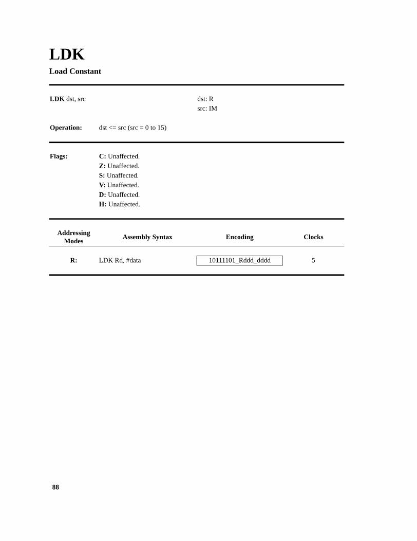
88
LDKLoad Constant
LDK dst, src dst: R
src: IM
Operation: dst <= src (src = 0 to 15)
Flags: C: Unaffected.
Z: Unaffected.
S: Unaffected.
V: Unaffected.
D: Unaffected.
H: Unaffected.
AddressingModes
Assembly Syntax Encoding Clocks
R: LDK Rd, #data 10111101_Rddd_dddd 5

89
LDMLoad Multiple - Registers From Memory
Notes:
1. Registers are loaded starting with Rd and increasing. R0 follows R15 in the case of a wrap-around.
2. There are no restrictions on the Rd and Rs registers.
3. Bits 15-12 and 7-4 of the second word of the opcode are ignored.
LDM dst, src, n dst: R
src: IR, DA, X
Operation: dst <= src (n words)
Flags: C: Unaffected.
Z: Unaffected.
S: Unaffected.
V: Unaffected.
D: Unaffected.
H: Unaffected.
AddressingModes
Assembly Syntax Encoding Clocks
IR: LDM Rd, @Rs, #n 00011100_Rsnz_0001 11 + 3n
0000_Rddd_0000_nnnn
DA: LDM Rd, address, #n 01011100_0000_0001 14 + 3n
0000_Rddd_0000_nnnn
address
X: LDM Rd, addr(Rs), #n 01011100_Rsnz_0001 15 + 3n
0000_Rddd_0000_nnnn
address

90
LDMLoad Multiple - Memory From Registers
Notes:
1. Registers are stored starting with Rd and increasing. R0 follows R15 in the case of a wrap-around.
2. There are no restrictions on the Rd and Rs registers.
3. Bits 15-12 and 7-4 of the second word of the opcode are ignored.
LDM dst, src, n dst: IR, DA, X
src: R
Operation: dst <= src (n words)
Flags: C: Unaffected.
Z: Unaffected.
S: Unaffected.
V: Unaffected.
D: Unaffected.
H: Unaffected.
AddressingModes
Assembly Syntax Encoding Clocks
IR: LDM @Rd, Rs, #n 00011100_Rdnz_1001 11 + 3n
0000_Rsss_0000_nnnn
DA: LDM address, Rs, #n 01011100_0000_1001 14 + 3n
0000_Rsss_0000_nnnn
address
X: LDM addr(Rd), Rs, #n 01011100_Rdnz_1001 15 + 3n
0000_Rsss_0000_nnnn
address

91
LDPSLoad Program Status
LDPS src src: IR, DA, X
Operation: PS <= src (FCW from src address, PC from subsequent address)
Flags: C: Loaded from src.
Z: Loaded from src.
S: Loaded from src.
V: Loaded from src.
D: Loaded from src.
H: Loaded from src.
AddressingModes
Assembly Syntax Encoding Clocks
IR: LDPS @Rs 00111001_Rsnz_0000 12
DA: LDPS address 01111001_0000_0000 16
address
X: LDPS addr(Rs) 01111001_Rsnz_0000 17
address

92
LDRLoad Relative Register
Notes:
1. The PC used for the address calculation is the PC of the next instruction.
2. The displacement is a 16-bit twos-complement number in the range -32768 to +32767. Thus the sourcemust be in the range -32766 to +32769 from the address of the LDR instruction.
3. Data is read from the program address space.
LDR dst, src dst: R
LDRB src: RA
LDRL
Operation: dst <= src
Flags: C: Unaffected.
Z: Unaffected.
S: Unaffected.
V: Unaffected.
D: Unaffected.
H: Unaffected.
AddressingModes
Assembly Syntax Encoding Clocks
RA: LDR Rd, address 00110001_0000_Rddd 14
displacement
LDRB Rbd, address 00110000_0000_Rbdd 14
displacement
LDRL RRd, address 00110101_0000_RRdd 17
displacement

93
LDRLoad Relative Memory
Notes:
1. The PC used for the address calculation is the PC of the next instruction.
2. The displacement is a 16-bit twos-complement number in the range -32768 to +32767. Thus the destina-tion must be in the range -32766 to +32769 from the address of the LDR instruction.
3. Data is read from the program address space.
LDR dst, src dst: RA
LDRB src: R
LDRL
Operation: dst <= src
Flags: C: Unaffected.
Z: Unaffected.
S: Unaffected.
V: Unaffected.
D: Unaffected.
H: Unaffected.
AddressingModes
Assembly Syntax Encoding Clocks
RA: LDR address, Rs 00110011_0000_Rsss 14
displacement
LDRB address, Rbs 00110010_0000_Rbss 14
displacement
LDRL address, RRs 00110111_0000_RRss 17
displacement

94
MBITMulti-Micro Bit Test
Notes:
1. The MIB input is sampled during the T1 state of this instruction.
MBIT
Operation: FCW[5] <= MIB
Flags: C: Unaffected.
Z: Unaffected.
S: Set if MIB is High, cleared otherwise.
V: Unaffected.
D: Unaffected.
H: Unaffected.
AddressingModes
Assembly Syntax Encoding Clocks
MBIT 01111011_0000_1010 7

95
MREQMulti-Micro Request
Notes:
1. Rd is unchanged if no request was signalled, and zero if a request was signalled.
2. This instruction is not interruptible and can take a long time to execute if the value in Rd is very big.
MREQ dst dst: R
Operation: if (!MIB) begin
FCW[6:5] <= 0x00 //request not signalled
MOB <= 1
end
else begin
MOB <= 0
dst <= dst - 1; repeat until dst = 0
if (!MIB) begin
FCW[6:5] <= 0x11 //request granted
end
else begin
FCW[6:5] <= 0x10 //request not granted
MOB <= 1
end
end
Flags: C: Unaffected.
Z: Set if request was signalled; cleared otherwise.
S: Set if request was signalled and granted; cleared otherwise.
V: Unaffected.
D: Unaffected.
H: Unaffected.
AddressingModes
Assembly Syntax Encoding Clocks
MREQ Rd 01111011_Rddd_1101 12 + 7n

96
MRESMulti-Micro Reset
Notes:
1. The MOB output changes state on the instruction boundary.
MRES
Operation: MOB <= High
Flags: C: Unaffected.
Z: Unaffected.
S: Unaffected.
V: Unaffected.
D: Unaffected.
H: Unaffected.
AddressingModes
Assembly Syntax Encoding Clocks
MRES 01111011_0000_1001 5

97
MSETMulti-Micro Set
Notes:
1. The MOB output changes state on the instruction boundary.
MSET
Operation: MOB <= Low
Flags: C: Unaffected.
Z: Unaffected.
S: Unaffected.
V: Unaffected.
D: Unaffected.
H: Unaffected.
AddressingModes
Assembly Syntax Encoding Clocks
MSET 01111011_0000_1000 5

98
MULTMultiply
MULT dst, src dst: R
MULTL src: R, IM, IR, DA, X
Operation: Word: dst[31:0] <= dst[15:0] x src[15:0]
Long: dst[63:0] <= dst[31:0] x src[31:0]
Flags: C: See tables below.
Z: Set if result is zero; cleared otherwise.
S: Set if result is negative; cleared otherwise.
V: Cleared.
D: Unaffected.
H: Unaffected.
AddressingModes
Assembly Syntax Encoding Clocks
R: MULT RRd, Rs 10011001_Rsss_RRdd 6 + mult
MULTL RQd, RRs 10011000_RRss_RQdd 6 + multl
IM: MULT RRd, #data 00011001_0000_RRdd 8 + mult
#data
MULTL RQd, #data 00011000_0000_RQdd 11 + multl
#data (high)
#data (low)
IR: MULT RRd, @Rs 00011001_Rsnz_RRdd 8 + mult
MULTL RQd, @Rs 00011000_Rsnz_RQdd 11 + multl
DA: MULT RRd, address 01011001_0000_RRdd 10 + mult
address
MULTL RQd, address 01011000_0000_RQdd 13 + mult
address

99
Notes:
1. All three numbers (multiplicand, multiplier and product) are signed twos-complement numbers.
2. The execution time and different C flag cases for MULT are shown in the table below:
4.The execution time and different C flag cases for MULTL are shown in the table below:
5. The execution time for MULTL is data-dependent. The m in the table below is the number of ones in theabsolute value of the multiplicand (dst[31:0]).
5. Because RRd (or RQd) and Rs (or RRs) are used to store intermediate results, they must be separate andnon-overlapping.
AddressingModes
Assembly Syntax Encoding Clocks
X: MULT RRd, addr(Rs) 01011001_Rsnz_RRdd 11 + mult
address
MULTL RQd, addr(Rs) 01011000_Rsnz_RQdd 14 + multl
address
MULT case C mult cycles
1. Product requires 32 bits. 1 63
2. Product is zero. 0 9
3. Product can be represented in 16 bits. Most significant word is merely sign-extension data.
0 63
MULTL case C multl cycles
1. Product requires 64 bits. 1 252 + 4m
2. Product is zero. 0 15
3. Product can be represented in 32 bits. Most significant two words are merely sign-extension data.
0 252 + 4m

100
NEGNegate
NEG dst dst: R, IR, DA, X
NEGB
Operation: dst <= 0 - dst
Flags: C: Set if result is zero; cleared otherwise (indicating borrow).
Z: Set if result is zero; cleared otherwise.
S: Set if result is negative; cleared otherwise.
V: Set if arithmetic overflow; cleared otherwise.
D: Unaffected.
H: Unaffected.
AddressingModes
Assembly Syntax Encoding Clocks
R: NEG Rd 10001101_Rddd_0010 7
NEGB Rbd 10001100_Rbdd_0010 7
IR: NEG @Rd 00001101_Rdnz_0010 12
NEGB @Rd 00001100_Rdnz_0010 12
DA: NEG address 01001101_0000_0010 15
address
NEGB address 01001100_0000_0010 15
address
X: NEG addr(Rd) 01001101_Rdnz_0010 16
address
NEGB addr(Rd) 01001100_Rdnz_0010 16
address

101
NOPNo operation
NOP
Operation: none
Flags: C: Unaffected.
Z: Unaffected.
S: Unaffected.
V: Unaffected.
D: Unaffected.
H: Unaffected.
AddressingModes
Assembly Syntax Encoding Clocks
NOP 10001101_0000_0111 7
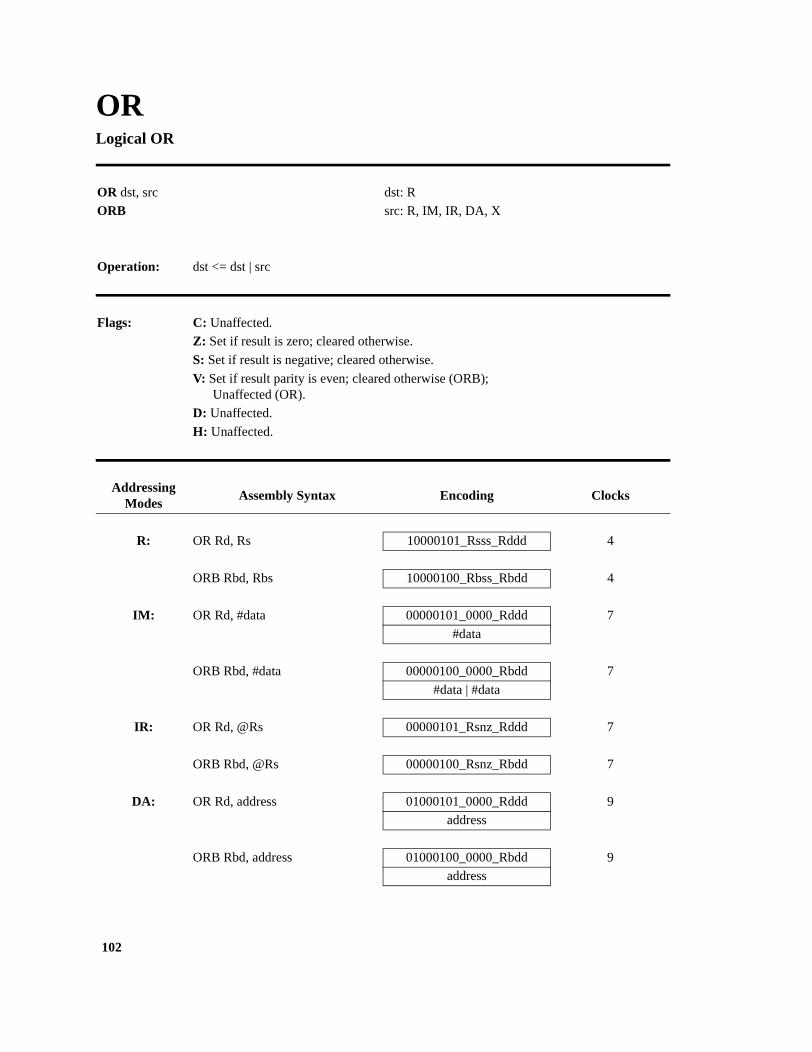
102
ORLogical OR
OR dst, src dst: R
ORB src: R, IM, IR, DA, X
Operation: dst <= dst | src
Flags: C: Unaffected.
Z: Set if result is zero; cleared otherwise.
S: Set if result is negative; cleared otherwise.
V: Set if result parity is even; cleared otherwise (ORB); Unaffected (OR).
D: Unaffected.
H: Unaffected.
AddressingModes
Assembly Syntax Encoding Clocks
R: OR Rd, Rs 10000101_Rsss_Rddd 4
ORB Rbd, Rbs 10000100_Rbss_Rbdd 4
IM: OR Rd, #data 00000101_0000_Rddd 7
#data
ORB Rbd, #data 00000100_0000_Rbdd 7
#data | #data
IR: OR Rd, @Rs 00000101_Rsnz_Rddd 7
ORB Rbd, @Rs 00000100_Rsnz_Rbdd 7
DA: OR Rd, address 01000101_0000_Rddd 9
address
ORB Rbd, address 01000100_0000_Rbdd 9
address

103
AddressingModes
Assembly Syntax Encoding Clocks
X: OR Rd, addr(Rs) 01000101_Rsnz_Rddd 10
address
ORB Rbd, addr(Rs) 01000100_Rsnz_Rbdd 10
address

104
(S)OTDR(Special) Output, Decrement and Repeat
Notes:
1. The Z8000 documentation lists the Z flag as undefined. In the Y8002 design this flag is unaffected.
OTDR dst, src, r dst: IR
OTDRB src: IR
SOTDRSOTDRB
Operation: dst <= src
Rs <= (Word) ? Rs -2 : Rs -1
r <= r - 1
repeat until r = 0
Flags: C: Unaffected.
Z: Unaffected.
S: Unaffected.
V: Set if r is zero after the decrement; cleared otherwise.
D: Unaffected.
H: Unaffected.
AddressingModes
Assembly Syntax Encoding Clocks
IR: OTDR @Rd, @Rs, r 00111011_Rsnz_1010 11 + 10n
0000_Rrrr_Rdnz_0000
SOTDR @Rd, @Rs, r 00111011_Rsnz_1011 11 + 10n
0000_Rrrr_Rdnz_0000
OTDRB @Rd, @Rs, r 00111010_Rsnz_1010
0000_Rrrr_Rdnz_0000 11 + 10n
SOTDRB @Rd, @Rs, r 00111010_Rsnz_1011 11 + 10n
0000_Rrrr_Rdnz_0000

105
Notes (continued):
2. Because the Rd, Rs and r registers are changed by the instruction, they must be separate and non-overlap-ping.
3. Bits 15-12 of the second word of the opcode are ignored.
4. This instruction samples interrupts during each iteration. If an interrupt is pending, the instruction isstopped and the interrupt accepted. The PC saved during the interrupt acknowledge cycle in this case is thePC of the running instruction, allowing the instruction to restart after the interrupt has been serviced.
5. Bits 3-0 of the second word of the opcode are actually a condition code. The result of this condition codecheck is ORed with the r = 0 check to determine if the instruction is complete. The bit combination 0000 isthe encoding for “False”, making this a repeating instruction.

106
(S)OTIR(Special) Output, Increment and Repeat
Notes:
1. The Z8000 documentation lists the Z flag as undefined. In the Y8002 design this flag is unaffected.
OTIR dst, src, r dst: IR
OTIRB src: IR
SOTIRSOTIRB
Operation: dst <= src
Rs <= (Word) ? Rs + 2 : Rs + 1
r <= r - 1
repeat until r = 0
Flags: C: Unaffected.
Z: Unaffected.
S: Unaffected.
V: Set if r is zero after the decrement; cleared otherwise.
D: Unaffected.
H: Unaffected.
AddressingModes
Assembly Syntax Encoding Clocks
IR: OTIR @Rd, @Rs, r 00111011_Rsnz_0010 11 + 10n
0000_Rrrr_Rdnz_0000
SOTIR @Rd, @Rs, r 00111011_Rsnz_0011 11 + 10n
0000_Rrrr_Rdnz_0000
OTIRB @Rd, @Rs, r 00111010_Rsnz_0010
0000_Rrrr_Rdnz_0000 11 + 10n
SOTIRB @Rd, @Rs, r 00111010_Rsnz_0011 11 + 10n
0000_Rrrr_Rdnz_0000

107
Notes (continued):
2. Because the Rd, Rs and r registers are changed by the instruction, they must be separate and non-overlap-ping.
3. Bits 15-12 of the second word of the opcode are ignored.
4. This instruction samples interrupts during each iteration. If an interrupt is pending, the instruction isstopped and the interrupt accepted. The PC saved during the interrupt acknowledge cycle in this case is thePC of the running instruction, allowing the instruction to restart after the interrupt has been serviced.
5. Bits 3-0 of the second word of the opcode are actually a condition code. The result of this condition codecheck is ORed with the r = 0 check to determine if the instruction is complete. The bit combination 0000 isthe encoding for “False”, making this a repeating instruction.

108
(S)OUT(Special) Output
OUT dst, src dst: IR, DA
OUTB src: R
SOUT dst, src dst: DA
SOUTB src: R
Operation: dst <= src
Flags: C: Unaffected.
Z: Unaffected.
S: Unaffected.
V: Unaffected.
D: Unaffected.
H: Unaffected.
AddressingModes
Assembly Syntax Encoding Clocks
R: OUT @Rd, Rs 00111111_Rdnz_Rsss 10
OUTB @Rd, Rbs 00111110_Rdnz_Rbss 10
DA: OUT port, Rst 00111011_Rsss_0110 12
port
SOUT port, Rst 00111011_Rsss_0111 12
port
OUTB port, Rbs 00111010_Rsss_0110 12
port
SOUTB port, Rbs 00111010_Rsss_0111 12
port

109
Notes:
1. The Z8000 documentation lists the Z flag as undefined. In the Y8002 design this flag is unaffected.
2. Data is written to the I/O or Special I/O address space. Only the status code is different between OUT andSOUT.
3. I/O writes always have one automatic WAIT state. This is included in the Cycles number above.

110
(S)OUTD(Special) Output and Decrement
Notes:
1. The Z8000 documentation lists the Z flag as undefined. In the Y8002 design this flag is unaffected.
OUTD dst, src, r dst: IR
OUTDB src: IR
SOUTDSOUTDB
Operation: dst <= src
Rs <= (Word) ? Rs - 2 : Rs - 1
r <= r - 1
Flags: C: Unaffected.
Z: Unaffected.
S: Unaffected.
V: Set if r is zero after the decrement; cleared otherwise.
D: Unaffected.
H: Unaffected.
AddressingModes
Assembly Syntax Encoding Clocks
IR: OUTD @Rd, @Rs, r 00111011_Rsnz_1010 21
0000_Rrrr_Rdnz_1000
SOUTD @Rd, @Rs, r 00111011_Rsnz_1011 21
0000_Rrrr_Rdnz_1000
OUTDB @Rd, @Rs, r 00111010_Rsnz_1010 21
0000_Rrrr_Rdnz_1000
SOUTDB @Rd, @Rs, r 00111010_Rsnz_1011 21
0000_Rrrr_Rdnz_1000

111
Notes (continued):
2. Because the Rd, Rs and r registers are changed by the instruction, they must be separate and non-overlap-ping.
3. Bits 15-12 of the second word of the opcode are ignored.
4. Bits 3-0 of the second word of the opcode are actually a condition code. The result of this condition codecheck is ORed with the r = 0 check to determine if the instruction is complete. The bit combination 1000 isthe encoding for “True”, making this a non-repeating instruction.

112
(S)OUTI(Special) Output and Increment
Notes:
1. The Z8000 documentation lists the Z flag as undefined. In the Y8002 design this flag is unaffected.
OUTI dst, src, r dst: IR
OUTIB src: IR
SOUTISOUTIB
Operation: dst <= src
Rs <= (Word) Rs + 2 : Rs + 1
r <= r - 1
Flags: C: Unaffected.
Z: Unaffected.
S: Unaffected.
V: Set if r is zero after the decrement; cleared otherwise.
D: Unaffected.
H: Unaffected.
AddressingModes
Assembly Syntax Encoding Clocks
IR: OUTI @Rd, @Rs, r 00111011_Rsnz_0010 21
0000_Rrrr_Rdnz_1000
SOUTI @Rd, @Rs, r 00111011_Rsnz_0011 21
0000_Rrrr_Rdnz_1000
OUTIB @Rd, @Rs, r 00111010_Rsnz_0010 21
0000_Rrrr_Rdnz_1000
SOUTIB @Rd, @Rs, r 00111010_Rsnz_0011 21
0000_Rrrr_Rdnz_1000

113
Notes (continued):
2. Because the Rd, Rs and r registers are changed by the instruction, they must be separate and non-overlap-ping.
3. Bits 15-12 of the second word of the opcode are ignored.
4. Bits 3-0 of the second word of the opcode are actually a condition code. The result of this condition codecheck is ORed with the r = 0 check to determine if the instruction is complete. The bit combination 1000 isthe encoding for “True”, making this a non-repeating instruction.

114
POPPop
POP dst, src dst: R, IR, DA, X
POPL src: IR
Operation: dst <= src
Rs <= (Long) ? Rs + 4 : Rs + 2
Flags: C: Unaffected.
Z: Unaffected.
S: Unaffected.
V: Unaffected.
D: Unaffected.
H: Unaffected.
AddressingModes
Assembly Syntax Encoding Clocks
R: POP Rd, @Rs 10010111_Rsnz_Rddd 8
POPL RRd, @Rs 10010101_Rsnz_RRdd 12
IR: POP @Rd, @Rs 00010111_Rsnz_Rdnz 12
POPL @Rd, @Rs 00010101_Rsnz_Rdnz 19
DA: POP address, @Rs 01010111_Rsnz_0000 16
address
POPL address, @Rs 01010101_Rsnz_0000 23
address
X: POP addr(Rd), @Rs 01010111_Rsnz_Rdnz 16
address
POPL addr(Rd), @Rs 01010101_Rsnz_Rdnz 23
address

115
Notes:
1. R0 cannot be used as a stack pointer. This limitation comes about because of the instruction encodingrules.
2. Because the Rd and Rs registers are changed by the instruction, they must be separate and non-overlap-ping.

116
PUSHPush
PUSH dst, src dst: IR
PUSHL src: R, IM, IR, DA, X
Operation: tmp <= src
Rd <= (Long) ? Rd - 4 : Rd - 2
dst <= tmp
Flags: C: Unaffected.
Z: Unaffected.
S: Unaffected.
V: Unaffected.
D: Unaffected.
H: Unaffected.
AddressingModes
Assembly Syntax Encoding Clocks
R: PUSH @Rd, Rs 10010011_Rdnz_Rsss 9
PUSHL @Rd, RRs 10010001_Rdnz_RRss 12
IM: PUSH @Rd, #data 00001101_Rdnz_1001 12
#data
IR: PUSH @Rd, @Rs 00010011_Rdnz_Rsnz 13
PUSHL @Rd, @Rs 00010001_Rdnz_Rsnz 20
DA: PUSH @Rd, address 01010011_Rdnz_0000 14
address
PUSHL @Rd, address 01010001_Rdnz_0000 21
address

117
Notes:
1. R0 cannot be used as a stack pointer. This limitation comes about because of the instruction encodingrules.
2. The Z8000 documentation states that the Rs and Rd registers must be separate and non-overlapping forPUSHL. This restriction is not present in the Y8002 design.
AddressingModes
Assembly Syntax Encoding Clocks
X: PUSH @Rd, addr(Rs) 01010011_Rdnz_Rsnz 14
address
PUSHL @Rd, addr(Rs) 01010001_Rdnz_Rsnz 21
address

118
RESReset Bit Static
RES dst, src dst: R, IR, DA, X
RESB src: IM
Operation: dst[src] <= 0
Flags: C: Unaffected.
Z: Unaffected.
S: Unaffected.
V: Unaffected.
D: Unaffected.
H: Unaffected.
AddressingModes
Assembly Syntax Encoding Clocks
R: RES Rd, #b 10100011_Rddd_bbbb 4
RESB Rbd, #b 10100010_Rbdd_0bbb 4
IR: RES @Rd, #b 00100011_Rdnz_bbbb 11
RESB @Rd, #b 00100010_Rdnz_0bbb 11
DA: RES address, #b 01100011_0000_bbbb 13
address
RESB address, #b 01100010_0000_0bbb 13
address
X: RES addr(Rd), #b 01100011_Rdnz_bbbb 14
address
RESB addr(Rd), #b 01100010_Rdnz_0bbb 14
address

119
Notes:
1. Only bits 2-0 of the opcode are used to select the bit in the case of RESB, and bit 3 of the opcode isignored.

120
RESReset Bit Dynamic
Notes:
1. The Z8000 microprocessor restricts the source register to be one of R0 - R7 for RESB. This restrictiondoes not apply to the Y8002 design. Any register may be used as the source.
2. Only bits 3-0 of the source operand are used for the bit select for RES; only bits 2-0 of the source operandare used for the bit select for RESB.
3. Only bits 11-8 of the second word of the opcode are used. All other bits in the second word of the opcodeare ignored.
RES dst, src dst: R
RESB src: R
Operation: dst[src] <= 0
Flags: C: Unaffected.
Z: Unaffected.
S: Unaffected.
V: Unaffected.
D: Unaffected.
H: Unaffected.
AddressingModes
Assembly Syntax Encoding Clocks
R: RES Rd, Rs 00100011_0000_Rsss 10
0000_Rddd_0000_0000
RESB Rbd, Rs 00100010_0000_Rsss 10
0000_Rbdd_0000_0000

121
RESFLGReset Flag
RESFLG flags flag: C, Z, S, P, V
Operation: FCW[7:4] <= FCW[7:4] & ~inst[7:4]
Flags: C: Cleared if specified; unaffected otherwise.
Z: Cleared if specified; unaffected otherwise.
S: Cleared if specified; unaffected otherwise.
V: Cleared if specified; unaffected otherwise.
D: Unaffected.
H: Unaffected.
AddressingModes
Assembly Syntax Encoding Clocks
RESFLG flags 10001101_CZSV_0011 7

122
RETReturn
Notes:
1. The execution time is 7 clocks if cc is false and 10 clocks if cc is true.
RET cc
Operation: if cc is true: PC <= @SP
SP <= SP + 2
Flags: C: Unaffected.
Z: Unaffected.
S: Unaffected.
V: Unaffected.
D: Unaffected.
H: Unaffected.
AddressingModes
Assembly Syntax Encoding Clocks
RET cc 10011110_0000_cccc 10/7

123
RLRotate Left
RL dst, src dst: R
RLB src: IM
Operation: Word: {C, dst[15:0]} <= {dst[15:0], dst[15]}; repeat if by 2
Byte: {C, dst[7:0]} <= {dst[7:0], dst[7]}; repeat if by 2
Flags: C: Set if carry from MSB for last rotate; cleared otherwise.
Z: Set if result is zero; cleared otherwise.
S: Set if result is negative; cleared otherwise.
V: Set if arithmetic overflow during rotate; cleared otherwise.
D: Unaffected.
H: Unaffected.
AddressingModes
Assembly Syntax Encoding Clocks
R: RL Rd, #1 10110011_Rddd_0000 6
RL Rd, #2 10110011_Rddd_0010 7
RLB Rbd, #1 10110010_Rbdd_0000 6
RLB Rbd, #2 10110010_Rbdd_0010 7

124
RLCRotate Left through Carry
RLC dst, src dst: R
RLCB src: IM
Operation: Word: {C, dst[15:0]} <= {dst[15:0], C}; repeat if by 2
Byte: {C, dst[7:0]} <= {dst[7:0], C}; repeat if by 2
Flags: C: Set if carry from MSB for last rotate; cleared otherwise.
Z: Set if result is zero; cleared otherwise.
S: Set if result is negative; cleared otherwise.
V: Set if arithmetic overflow during rotate; cleared otherwise.
D: Unaffected.
H: Unaffected.
AddressingModes
Assembly Syntax Encoding Clocks
R: RLC Rd, #1 10110011_Rddd_1000 6
RLC Rd, #2 10110011_Rddd_1010 7
RLCB Rbd, #1 10110010_Rbdd_1000 6
RLCB Rbd, #2 10110010_Rbdd_1010 7

125
RLDBRotate Left Digit
RLDB dst, src dst: R
src: R
Operation: {dst[7:0], src[7:0]} <= {dst[7:4], src[7:0], dst[3:0]};
Flags: C: Unaffected.
Z: Set if dst is zero after rotate; cleared otherwise.
S: Unaffected.
V: Unaffected.
D: Unaffected.
H: Unaffected.
AddressingModes
Assembly Syntax Encoding Clocks
R: RLDB Rbd, Rbs 10111110_Rbss_Rbdd 9

126
RRRotate Right
RRC dst, src dst: R
RRCB src: IM
Operation: Word: {dst[15:0], C} <= {dst[0], dst[15:0]}; repeat if by 2
Byte: {dst[7:0], C} <= {dst[0], dst[7:0]}; repeat if by 2
Flags: C: Set if carry from LSB for last rotate; cleared otherwise.
Z: Set if result is zero; cleared otherwise.
S: Set if result is negative; cleared otherwise.
V: Set if arithmetic overflow during rotate; cleared otherwise.
D: Unaffected.
H: Unaffected.
AddressingModes
Assembly Syntax Encoding Clocks
R: RR Rd, #1 10110011_Rddd_0100 6
RR Rd, #2 10110011_Rddd_0110 7
RRB Rbd, #1 10110010_Rbdd_0100 6
RRB Rbd, #2 10110010_Rbdd_0110 7

127
RRCRotate Right through Carry
RRC dst, src dst: R
RRCB src: IM
Operation: Word: {dst[15:0], C} <= {C, dst[15:0]}; repeat if by 2
Byte: {dst[7:0], C} <= {C, dst[7:0]}; repeat if by 2
Flags: C: Set if carry from LSB for last rotate; cleared otherwise.
Z: Set if result is zero; cleared otherwise.
S: Set if result is negative; cleared otherwise.
V: Set if arithmetic overflow during rotate; cleared otherwise.
D: Unaffected.
H: Unaffected.
AddressingModes
Assembly Syntax Encoding Clocks
R: RRC Rd, #1 10110011_Rddd_1100 6
RRC Rd, #2 10110011_Rddd_1110 7
RRCB Rbd, #1 10110010_Rbdd_1100 6
RRCB Rbd, #2 10110010_Rbdd_1110 7

128
RRDBRotate Right Digit
RLDB dst, src dst: R
src: R
Operation: {dst[7:0], src[7:0]} <= {dst[7:4], src[3:0], dst[3:0], src[7:4]};
Flags: C: Unaffected.
Z: Set if dst is zero after rotate; cleared otherwise.
S: Unaffected.
V: Unaffected.
D: Unaffected.
H: Unaffected.
AddressingModes
Assembly Syntax Encoding Clocks
R: RRDB Rbd, Rbs 10111100_Rbss_Rbdd 9

129
SBCSubtract With Carry
SBC dst, src dst: R
SBCB src: R
Operation: dst <= dst - src - C
Flags: C: Cleared if arithmetic carry from result MSB; set otherwise, indicating borrow.
Z: Set if result is zero; cleared otherwise.
S: Set if result is negative; cleared otherwise.
V: Set if arithmetic overflow; cleared otherwise.
D: Set (SBCB); Unaffected (SBC).
H: Cleared if arithmetic carry from bit 3; set otherwise, indicating borrow (SBCB); Unaffected (SBC).
AddressingModes
Assembly Syntax Encoding Clocks
R: SBC Rd, Rs 10110111_Rsss_Rddd 5
SBCB Rbd, Rbs 10110110_Rbss_Rbdd 5

130
SCSystem Call
Notes:
1. Bits 7-0 of the opcode can be used by the trap handler software to encode the type of System Call beingrequested. The entire opcode is pushed onto the system stack.
2. Version 1 of the Y8002 uses the System Call entry in the Program Status Area for all Unimplemented andReserved opcodes. All of these opcodes can be distinguished from an actual System Call by inspecting theopcode word pushed onto the system stack. Refer to the appropriate Appendix for a list of all Unimple-mented and Reserved opcodes.
SC src src: IM
Operation: SP <= SP - 2
@SP <= PC
SP <= SP - 2
@SP <= FCW
SP <= SP - 2
@SP <= inst
FCW <= @{PSAP, 0x0C}
PC <= @{PSAP, 0x0E}
Flags: C: Unaffected.
Z: Unaffected.
S: Unaffected.
V: Unaffected.
D: Unaffected.
H: Unaffected.
AddressingModes
Assembly Syntax Encoding Clocks
IM: SC #src 01111111_ssssrccc 33

131
SDAShift Dynamic Arithmetic
SDA dst, src dst: R
SDAB src: R
SDAL
Operation: src zero:
Word: {C, dst[15:0]} <= {C, dst[15:0]}
Byte: {C, dst[7:0]} <= {C, dst[7:0]}
Long: {C, dst[31:0]} <= {C, dst[31:0]}
src positive:
Word: (do src times): {C, dst[15:0]} <= {dst[15:0], 0}
Byte: (do src times): {C, dst[7:0]} <= {dst[7:0], 0}
Long: (do src times): {C, dst[31:0]} <= {dst[31:0], 0}
src negative:
Word: (do src times): {dst[15:0], C} <= {dst[15], dst[15:0]}
Byte: (do src times): {dst[7:0], C} <= {dst[7], dst[7:0]}
Long: (do src times): {dst[31:0], C} <= {dst[31], dst[31:0]}
Flags:C: Unaffected (src zero, Long only); set if carry from LSB (src negative) or MSB (src positive) on last shift; cleared otherwise.
Z: Set if result is zero; cleared otherwise.
S: Set if result is negative; cleared otherwise.
V: Set if arithmetic overflow during shift; cleared otherwise.
D: Unaffected.
H: Unaffected.
AddressingModes
Assembly Syntax Encoding Clocks
R: SDA Rd, Rs 10110011_Rddd_1011 15 + 3n
0000_Rsss_0000_0000
SDAB Rbd, Rs 10110010_Rbdd_1011 15 + 3n
0000_Rsss_0000_0000
SDAL RRd, Rs 10110011_RRdd_1111 15 + 3n
0000_Rsss_0000_0000

132
Notes:
1. The Z8000 documentation lists the C flag as undefined for zero shift. In fact it is always cleared for Byteor Word shifts of zero bit positions, and unaffected for a Long shift of zero bit positions. The Y8002 designmatches this behavior
2. The shift count should be restricted to range from -16 to 16 for SDA, from -8 to 8 for SDAB and from -32to 32 for SDAL. However, the entire 16-bit value in the src register is used as the starting count for the shift,so values outside of these ranges will still execute.
3. Only bits 11-8 of the second word of the opcode are used. All other bits in the second word of the opcodeare ignored.

133
SDLShift Dynamic Logical
SDL dst, src dst: R
SDLB src: R
SDLL
Operation: src zero:
Word: {C, dst[15:0]} <= {C, dst[15:0]}
Byte: {C, dst[7:0]} <= {C, dst[7:0]}
Long: {C, dst[31:0]} <= {C, dst[31:0]}
src positive:
Word: (do src times): {C, dst[15:0]} <= {dst[15:0], 0}
Byte: (do src times): {C, dst[7:0]} <= {dst[7:0], 0}
Long: (do src times): {C, dst[31:0]} <= {dst[31:0], 0}
src negative:
Word: (do src times): {dst[15:0], C} <= {0, dst[15:0]}
Byte: (do src times): {dst[7:0], C} <= {0, dst[7:0]}
Long: (do src times): {dst[31:0], C} <= {0, dst[31:0]}
Flags:C: Unaffected (src zero); set if carry from LSB (src negative) or MSB (src positive) on last shift; cleared otherwise.
Z: Set if result is zero; cleared otherwise.
S: Set if result is negative; cleared otherwise.
V: Set if arithmetic overflow during shift; cleared otherwise.
D: Unaffected.
H: Unaffected.
AddressingModes
Assembly Syntax Encoding Clocks
R: SDL Rd, Rs 10110011_Rddd_0011 15 + 3n
0000_Rsss_0000_0000
SDLB Rbd, Rs 10110010_Rbdd_0011 15 + 3n
0000_Rsss_0000_0000
SDLL RRd, Rs 10110011_RRdd_0111 15 + 3n
0000_Rsss_0000_0000

134
Notes:
1. The Z8000 documentation lists the V flag as undefined. In fact it signals arithmetic overflow, even thoughthis is a logical operation. The Y8002 design matches this behavior.
1. The Z8000 documentation lists the C flag as undefined for zero shift. In fact it is always cleared for Byteor Word shifts of zero bit positions, and unaffected for a Long shift of zero bit positions. The Y8002 designmatches this behavior
3. The shift count should be restricted to range from -16 to 16 for SDL, from -8 to 8 for SDLB and from -32to 32 for SDLL. However, the entire 16-bit value in the src register is used as the starting count for the shift,so values outside of these ranges will still execute.
4. Only bits 11-8 of the second word of the opcode are used. All other bits in the second word of the opcodeare ignored.

135
SETSet Bit Static
SET dst, src dst: R, IR, DA, X
SETB src: IM
Operation: dst[src] <= 1
Flags: C: Unaffected.
Z: Unaffected.
S: Unaffected.
V: Unaffected.
D: Unaffected.
H: Unaffected.
AddressingModes
Assembly Syntax Encoding Clocks
R: SET Rd, #b 10100101_Rddd_bbbb 4
SETB Rbd, #b 10100100_Rbdd_0bbb 4
IR: SET @Rd, #b 00100101_Rdnz_bbbb 11
SETB @Rd, #b 00100100_Rdnz_0bbb 11
DA: SET address, #b 01100101_0000_bbbb 13
address
SETB address, #b 01100100_0000_0bbb 13
address
X: SET addr(Rd), #b 01100101_Rdnz_bbbb 14
address
SETB addr(Rd), #b 01100100_Rdnz_0bbb 14
address

136
Notes:
1. Only bits 2-0 of the opcode are used to select the bit in the case of SETB, and bit 3 of the opcode isignored.
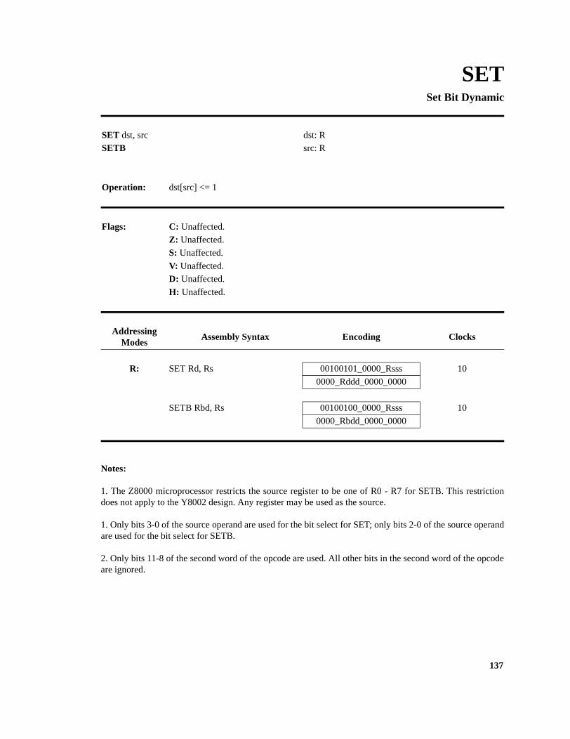
137
SETSet Bit Dynamic
Notes:
1. The Z8000 microprocessor restricts the source register to be one of R0 - R7 for SETB. This restrictiondoes not apply to the Y8002 design. Any register may be used as the source.
1. Only bits 3-0 of the source operand are used for the bit select for SET; only bits 2-0 of the source operandare used for the bit select for SETB.
2. Only bits 11-8 of the second word of the opcode are used. All other bits in the second word of the opcodeare ignored.
SET dst, src dst: R
SETB src: R
Operation: dst[src] <= 1
Flags: C: Unaffected.
Z: Unaffected.
S: Unaffected.
V: Unaffected.
D: Unaffected.
H: Unaffected.
AddressingModes
Assembly Syntax Encoding Clocks
R: SET Rd, Rs 00100101_0000_Rsss 10
0000_Rddd_0000_0000
SETB Rbd, Rs 00100100_0000_Rsss 10
0000_Rbdd_0000_0000

138
SETFLGSet Flag
SETFLG flags flag: C, Z, S, P, V
Operation: FCW[7:4] <= FCW[7:4] | inst[7:4]
Flags: C: Set if specified; unaffected otherwise.
Z: Set if specified; unaffected otherwise.
S: Set if specified; unaffected otherwise.
V: Set if specified; unaffected otherwise.
D: Unaffected.
H: Unaffected.
AddressingModes
Assembly Syntax Encoding Clocks
SETFLG flags 10001101_CZSV_0001 7

139
SLAShift Left Arithmetic
SLA dst, src dst: R
SLAB src: IM
SLAL
Operation: For src zero:
Word: {C, dst[15:0]} <= {C, dst[15:0]}
Byte: {C, dst[7:0]} <= {C, dst[7:0]}
Long: {C, dst[31:0]} <= {C, dst[31:0]}
Else:
Word: (do src times): {C, dst[15:0]} <= {dst[15:0], 0}
Byte: (do src times): {C, dst[7:0]} <= {dst[7:0], 0}
Long: (do src times): {C, dst[31:0]} <= {dst[31:0], 0}
Flags: C: Unaffected (src zero); set if carry from MSB on last shift; cleared otherwise.
Z: Set if result is zero; cleared otherwise.
S: Set if result is negative; cleared otherwise.
V: Set if arithmetic overflow during shift; cleared otherwise.
D: Unaffected.
H: Unaffected.
AddressingModes
Assembly Syntax Encoding Clocks
R: SLA Rd, #b 10110011_Rddd_1001
b
SLAB Rbd, #b 10110010_Rbdd_1001
0 | b
SLAL RRd, #b 10110011_RRdd_1101
b

140
Notes:
1. The shift count should be restricted to range from 0 to 16 for SLA, from 0 to 8 for SLAB and from 0 to 32for SLAL. However, the entire 16-bit value (Word or Long) or 8-bit value (Byte) in the second word of theinstruction is used as the starting count for the shift, so values outside of these ranges will still execute.
2. Only bits 7-0 of the second word of the opcode are used for SLAB. All other bits in the second word ofthe opcode are ignored in this case.

141
SLLShift Left Logical
Notes:
1. The Z8000 documentation lists the V flag as undefined. In fact it signals arithmetic overflow, even thoughthis is a logical operation. The Y8002 design matches this behavior.
SLL dst, src dst: R
SLLB src: IM
SLLL
Operation: For src zero:
Word: {C, dst[15:0]} <= {C, dst[15:0]}
Byte: {C, dst[7:0]} <= {C, dst[7:0]}
Long: {C, dst[31:0]} <= {C, dst[31:0]}
Else:
Word: (do src times): {C, dst[15:0]} <= {dst[15:0], 0}
Byte: (do src times): {C, dst[7:0]} <= {dst[7:0], 0}
Long: (do src times): {C, dst[31:0]} <= {dst[31:0], 0}
Flags: C: Unaffected (src zero); set if carry from MSB on last shift; cleared otherwise.
Z: Set if result is zero; cleared otherwise.
S: Set if result is negative; cleared otherwise.
V: Set if arithmetic overflow during shift; cleared otherwise.
D: Unaffected.
H: Unaffected.
AddressingModes
Assembly Syntax Encoding Clocks
R: SLA Rd, #b 10110011_Rddd_0001 13 + 3b
b
SLLB Rbd, #b 10110010_Rbdd_0001 13 + 3b
0 | b
SLLL RRd, #b 10110011_RRdd_0101 13 + 3b
b

142
Notes: (continued)
2. The shift count should be restricted to range from 0 to 16 for SLL, from 0 to 8 for SLLB and from 0 to 32for SLLL. However, the entire 16-bit value (Word or Long) or 8-bit value (Byte) in the second word of theinstruction is used as the starting count for the shift, so values outside of these ranges will still execute.
3. Only bits 7-0 of the second word of the opcode are used for SLLB. All other bits in the second word of theopcode are ignored in this case.

143
SRAShift Right Arithmetic
Notes:
1. The shift count should be restricted to range from 1 to 16 for SRA, from 1 to 16 for SRAB and from 1 to32 for SRAL. However, the entire 16-bit value (for Word or Long) or 8-bit value (for Byte) in the secondword of the instruction is used as the starting count for the shift, so values outside of these ranges will stillexecute. Note that b is negative in the opcode.
2. Only bits 7-0 of the second word of the opcode are used for SRAB. All other bits in the second word ofthe opcode are ignored in this case.
SRA dst, src dst: R
SRAB src: IM
SRAL
Operation: Word: (do src times): {dst[15:0], C} <= {dst[15], dst[15:0]}
Byte: (do src times): {dst[7:0], C} <= {dst[7], dst[7:0]}
Long: (do src times): {dst[31:0], C} <= {dst[31], dst[31:0]}
Flags: C: Set if carry from LSB on last shift; cleared otherwise.
Z: Set if result is zero; cleared otherwise.
S: Set if result is negative; cleared otherwise.
V: Cleared.
D: Unaffected.
H: Unaffected.
AddressingModes
Assembly Syntax Encoding Clocks
R: SRA Rd, #b 10110011_Rddd_1001 13 + 3b
-b
SRAB Rbd, #b 10110010_Rbdd_1001 13 + 3b
0 | -b
SRAL RRd, #b 10110011_RRdd_1101 13 + 3b
-b

144
SRLShift Right Logical
Notes:
1. The Z8000 documentation lists the V flag as undefined. In fact it signals arithmetic overflow, even thoughthis is a logical operation. The Y8002 design matches this behavior.
2. The shift count should be restricted to range from 1 to 16 for SRL, from 1 to 8 for SRLB and from 1 to 32for SRLL. However, the entire 16-bit value (Word or Long) or 8-bit value (Byte) in the second word of theinstruction is used as the starting count for the shift, so values outside of these ranges will still execute. Notethat b is negative in the opcode.
SRL dst, src dst: R
SRLB src: IM
SRLL
Operation: Word: (do src times): {dst[15:0], C} <= {0, dst[15:0]}
Byte: (do src times): {dst[7:0], C} <= {0, dst[7:0]}
Long: (do src times): {dst[31:0], C} <= {0, dst[31:0]}
Flags: C: Set if carry from LSB on last shift; cleared otherwise.
Z: Set if result is zero; cleared otherwise.
S: Set if result is negative; cleared otherwise.
V: Set if arithmetic overflow during shift; cleared otherwise.
D: Unaffected.
H: Unaffected.
AddressingModes
Assembly Syntax Encoding Clocks
R: SRL Rd, #b 10110011_Rddd_0001 13 + 3b
-b
SRLB Rbd, #b 10110010_Rbdd_0001 13 + 3b
0 | -b
SRLL RRd, #b 10110011_RRdd_0101 13 + 3b
-b

145
Notes (continued):
3. Only bits 7-0 of the second word of the opcode are used for SRLB. All other bits in the second word of theopcode are ignored in this case.

146
SUBSubtract
SUB dst, src dst: R
SUBB src: R, IM, IR, DA, X
SUBL
Operation: dst <= dst - src
Flags: C: Cleared if arithmetic carry from MSB; set otherwise, indicating borrow.
Z: Set if result is zero; cleared otherwise.
S: Set if result is negative; cleared otherwise.
V: Set if arithmetic overflow; cleared otherwise.
D: Set (SUBB); Unaffected (SUB).
H: Cleared if arithmetic carry from bit 3; set otherwise, indicating borrow (SUBB); Unaffected (SUB).
AddressingModes
Assembly Syntax Encoding Clocks
R: SUB Rd, Rs 10000011_Rsss_Rddd 4
SUBB Rbd, Rbs 10000010_Rbss_Rbdd 4
SUBL RRd, RRs 10010010_RRss_RRdd 8
IM: SUB Rd, #data 00000011_0000_Rddd 7
#data
SUBB Rbd, #data 00000010_0000_Rbdd 7
#data | #data
SUBL RRd, #data 00010010_0000_RRdd 14
#data (high)
#data (low)

147
AddressingModes
Assembly Syntax Encoding Clocks
IR: SUB Rd, @Rs 00000011_Rsnz_Rddd 7
SUBB Rbd, @Rs 00000010_Rsnz_Rbdd 7
SUBL RRd, @Rs 00010010_Rsnz_RRdd 14
DA: SUB Rd, address 01000011_0000_Rddd 9
address
SUBB Rbd, address 01000010_0000_Rbdd 9
address
SUBL RRd, address 01010010_0000_RRdd 15
address
X: SUB Rd, addr(Rs) 01000011_Rsnz_Rddd 10
address
SUBB Rbd, addr(Rs) 01000010_Rsnz_Rbdd 10
address
SUBL RRd, addr(Rs) 01010010_Rsnz_RRdd 16
address

148
TCCTest Condition Code
TCC cc, dst dst: R
TCCB
Operation: if cc true: dst[0] <= 1
Flags: C: Unaffected.
Z: Unaffected.
S: Unaffected.
V: Unaffected.
D: Unaffected.
H: Unaffected.
AddressingModes
Assembly Syntax Encoding Clocks
R: TCC cc, Rd 10101111_Rddd_cccc 5
TCCB cc, Rbd 10101110_Rbdd_cccc 5

149
TESTTest
TEST dst dst: R, IR, DA, X
TESTB
TESTL
Operation: dst | 0
Flags: C: Unaffected.
Z: Set if result is zero; cleared otherwise.
S: Set if result is negative; cleared otherwise.
V: Set if result parity is even; cleared otherwise (TESTB); Unaffected (TEST or TESTL).
D: Unaffected.
H: Unaffected.
AddressingModes
Assembly Syntax Encoding Clocks
R: TEST Rd 10001101_Rddd_0100 7
TESTB Rbd 10001100_Rbdd_0100 7
TESTL RRd 10011100_RRdd_1000 9
IR: TEST @Rd 00001101_Rdnz_0100 8
TESTB @Rd 00001100_Rdnz_0100 8
TESTL @Rd 00011100_Rdnz_1000 13
DA: TEST address 01001101_0000_0100 11
address
TESTB address 01001100_0000_0100 11
address
TESTL address 01011100_0000_1000 16
address

150
AddressingModes
Assembly Syntax Encoding Clocks
X: TEST addr(Rd) 01001101_Rdnz_0100 12
address
TESTB addr(Rd) 01001100_Rdnz_0100 12
address
TESTL addr(Rd) 01011100_Rddd_1000 17
address

151
TRDBTranslate and Decrement
Notes:
1. Because the Rd, Rs and r registers are changed by the instruction, they must be separate and non-overlap-ping.
2. Bits 15-12 and 3-0 of the second word of the opcode are ignored.
TRDB dst, src, r dst: IR
src: IR
Operation: dst <= src[dst]
Rd <= Rd - 1
r <= r - 1
Flags: C: Unaffected.
Z: Unaffected.
S: Unaffected.
V: Set if r is zero after the decrement; cleared otherwise.
D: Unaffected.
H: Unaffected.
AddressingModes
Assembly Syntax Encoding Clocks
IR: TRDB @Rd, @Rs, r 10111000_Rdnz_1000 25
0000_Rrrr_Rsnz_0000

152
TRDRBTranslate, Decrement and Repeat
Notes:
1. Because the Rd, Rs and r registers are changed by the instruction, they must be separate and non-overlap-ping.
2. Bits 15-12 and 3-0 of the second word of the opcode are ignored.
3. This instruction samples interrupts during each iteration. If an interrupt is pending, the instruction isstopped and the interrupt accepted. The PC saved during the interrupt acknowledge cycle in this case is thePC of the running instruction, allowing the instruction to restart after the interrupt has been serviced.
TRDRB dst, src, r dst: IR
src: IR
Operation: dst <= src[dst]
Rd <= Rd - 1
r <= r - 1
repeat until r = 0
Flags: C: Unaffected.
Z: Unaffected.
S: Unaffected.
V: Set if r is zero after the decrement; cleared otherwise.
D: Unaffected.
H: Unaffected.
AddressingModes
Assembly Syntax Encoding Clocks
IR: TRDRB @Rd, @Rs, r 10111000_Rdnz_1100 11 + 14n
0000_Rrrr_Rsnz_0000

153
TRIBTranslate and Increment
Notes:
1. Because the Rd, Rs and r registers are changed by the instruction, they must be separate and non-overlap-ping.
2. Bits 15-12 and 3-0 of the second word of the opcode are ignored.
TRIB dst, src, r dst: IR
src: IR
Operation: dst <= src[dst]
Rs <= Rs + 1
r <= r - 1
Flags: C: Unaffected.
Z: Unaffected.
S: Unaffected.
V: Set if r is zero after the decrement; cleared otherwise.
D: Unaffected.
H: Unaffected.
AddressingModes
Assembly Syntax Encoding Clocks
IR: TRIB @Rd, @Rs, r 10111000_Rdnz_0000 25
0000_Rrrr_Rsnz_0000

154
TRIRBTranslate, Increment and Repeat
Notes:
1. Because the Rd, Rs and r registers are changed by the instruction, they must be separate and non-overlap-ping.
2. Bits 15-12 and 3-0 of the second word of the opcode are ignored.
3. This instruction samples interrupts during each iteration. If an interrupt is pending, the instruction isstopped and the interrupt accepted. The PC saved during the interrupt acknowledge cycle in this case is thePC of the running instruction, allowing the instruction to restart after the interrupt has been serviced.
TRIRB dst, src, r dst: IR
src: IR
Operation: dst <= src[dst]
Rd <= Rd + 1
r <= r - 1
repeat until r = 0
Flags: C: Unaffected.
Z: Unaffected.
S: Unaffected.
V: Set if r is zero after the decrement; cleared otherwise.
D: Unaffected.
H: Unaffected.
AddressingModes
Assembly Syntax Encoding Clocks
IR: TRIRB @Rd, @Rs, r 10111000_Rdnz_0100 11 + 14n
0000_Rrrr_Rsnz_0000
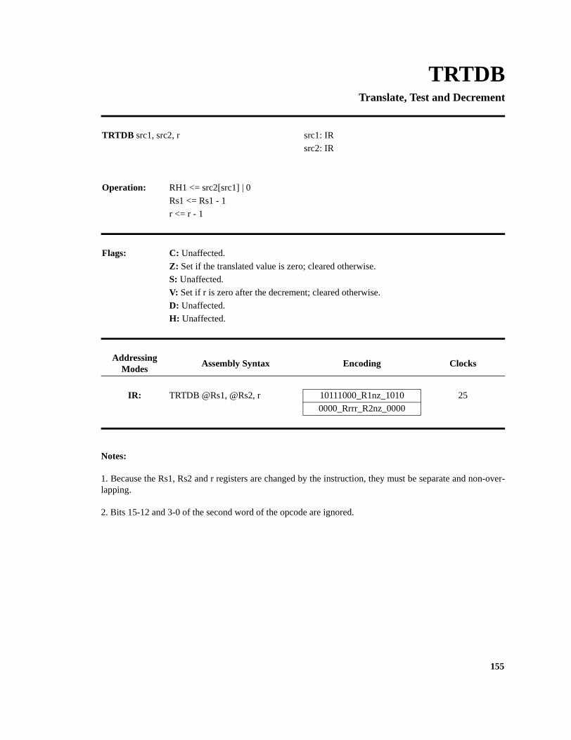
155
TRTDBTranslate, Test and Decrement
Notes:
1. Because the Rs1, Rs2 and r registers are changed by the instruction, they must be separate and non-over-lapping.
2. Bits 15-12 and 3-0 of the second word of the opcode are ignored.
TRTDB src1, src2, r src1: IR
src2: IR
Operation: RH1 <= src2[src1] | 0
Rs1 <= Rs1 - 1
r <= r - 1
Flags: C: Unaffected.
Z: Set if the translated value is zero; cleared otherwise.
S: Unaffected.
V: Set if r is zero after the decrement; cleared otherwise.
D: Unaffected.
H: Unaffected.
AddressingModes
Assembly Syntax Encoding Clocks
IR: TRTDB @Rs1, @Rs2, r 10111000_R1nz_1010 25
0000_Rrrr_R2nz_0000

156
TRTDRBTranslate, Test, Decrement and Repeat
Notes:
1. Because the Rs1, Rs2 and r registers are changed by the instruction, they must be separate and non-over-lapping.
2. Bits 15-12 of the second word of the opcode are ignored.
3. There is no obvious reason why bits 3-0 of the second word of the opcode must be 1110, and the Y8002actually ignores these four bits.
4. This instruction samples interrupts during each iteration. If an interrupt is pending, the instruction isstopped and the interrupt accepted. The PC saved during the interrupt acknowledge cycle in this case is thePC of the running instruction, allowing the instruction to restart after the interrupt has been serviced.
TRTDRB src1, src2, r src1: IR
src2: IR
Operation: RH1 <= src2[src1] | 0
Rs1 <= Rs1 - 1
r <= r - 1
repeat until translated value is zero or r is zero after decrement; cleared otherwise.
Flags: C: Unaffected.
Z: Set if the translated value is zero; cleared otherwise.
S: Unaffected.
V: Set if r is zero after the decrement; cleared otherwise.
D: Unaffected.
H: Unaffected.
AddressingModes
Assembly Syntax Encoding Clocks
IR: TRTDRB @Rs1, @Rs2, r 10111000_R1nz_1110 11 + 14n
0000_Rrrr_R2nz_1110

157
TRTIBTranslate, Test and Increment
Notes:
1. Because the Rs1, Rs2 and r registers are changed by the instruction, they must be separate and non-over-lapping.
2. Bits 15-12 and 3-0 of the second word of the opcode are ignored.
TRTIB src1, src2, r src1: IR
src2: IR
Operation: RH1 <= src2[src1] | 0
Rs1 <= Rs1 + 1
r <= r - 1
Flags: C: Unaffected.
Z: Set if the translated value is zero; cleared otherwise.
S: Unaffected.
V: Set if r is zero after the decrement; cleared otherwise.
D: Unaffected.
H: Unaffected.
AddressingModes
Assembly Syntax Encoding Clocks
IR: TRTIB @Rs1, @Rs2, r 10111000_R1nz_0010 25
0000_Rrrr_R2nz_0000

158
TRTIRBTranslate, Test, Increment and Repeat
Notes:
1. Because the Rs1, Rs2 and r registers are changed by the instruction, they must be separate and non-over-lapping.
2. Bits 15-12 of the second word of the opcode are ignored.
3. There is no obvious reason why bits 3-0 of the second word of the opcode must be 1110, and the Y8002actually ignores these four bits.
4. This instruction samples interrupts during each iteration. If an interrupt is pending, the instruction isstopped and the interrupt accepted. The PC saved during the interrupt acknowledge cycle in this case is thePC of the running instruction, allowing the instruction to restart after the interrupt has been serviced.
TRTIRB src1, src2, r src1: IR
src2: IR
Operation: RH1 <= src2[src1] | 0
Rs1 <= Rs1 + 1
r <= r - 1
repeat until translated value is zero or r is zero after decrement; cleared otherwise.
Flags: C: Unaffected.
Z: Set if the translated value is zero; cleared otherwise.
S: Unaffected.
V: Set if r is zero after the decrement; cleared otherwise.
D: Unaffected.
H: Unaffected.
AddressingModes
Assembly Syntax Encoding Clocks
IR: TRTIRB @Rs1, @Rs2, r 10111000_R1nz_0110 11 + 14n
0000_Rrrr_R2nz_1110

159
TSETTest and Set
TEST dst dst: R, IR, DA, X
TESTB
Operation: Word: S <= dst[15], dst <= 0xFFFFh
Byte: S <= dst[7], dst <= 0xFFh
Flags: C: Unaffected.
Z: Unaffected.
S: Set if MSB of dst was 1; cleared otherwise.
V: Unaffected.
D: Unaffected.
H: Unaffected.
AddressingModes
Assembly Syntax Encoding Clocks
R: TSET Rd 10001101_Rddd_0110 7
TSETB Rbd 10001100_Rbdd_0110 7
IR: TSET @Rd 00001101_Rdnz_0110 11
TSETB @Rd 00001100_Rdnz_0110 11
DA: TSET address 01001101_0000_0110 14
address
TSETB address 01001100_0000_0110 14
address
X: TSET addr(Rd) 01001101_Rdnz_0110 15
address
TSETB addr(Rd) 01001100_Rdnz_0110 15
address

160
Notes:
1. BUSREQ is not accepted between the read and write of the destination.
2. The Z8004 microprocessor actually signals a special status code (0xF) for the read and write of a TSETinstruction. The Y8002 design does not do this, instead matching the operation of the Z8002 microprocessorand signalling either Data or Stack memory address space.

161
XORLogical Exclusive-OR
XOR dst, src dst: R
XORB src: R, IM, IR, DA, X
Operation: dst <= dst ^ src
Flags: C: Unaffected.
Z: Set if result is zero; cleared otherwise.
S: Set if result is negative; cleared otherwise.
V: Set if result parity is even; cleared otherwise (XORB); Unaffected (XOR).
D: Unaffected.
H: Unaffected.
AddressingModes
Assembly Syntax Encoding Clocks
R: XOR Rd, Rs 10001001_Rsss_Rddd 4
XORB Rbd, Rbs 10001000_Rbss_Rbdd 4
IM: XOR Rd, #data 00001001_0000_Rddd 7
#data
XORB Rbd, #data 00001000_0000_Rddd 7
#data | #data
IR: XOR Rd, @Rs 00001001_Rsnz_Rddd 7
XORB Rbd, @Rs 00001000_Rsnz_Rbdd 7
DA: XOR Rd, address 01001001_0000_Rddd 9
address
XORB Rbd, address 01001000_0000_Rbdd 9
address

162
AddressingModes
Assembly Syntax Encoding Clocks
X: XOR Rd, addr(Rs) 01001001_Rsnz_Rddd 10
address
XORB Rbd, addr(Rs) 01001000_Rsnz_Rbdd 10
address

163
Extended InstructionLoad from EPU
Notes:
1. Bits 1-0 of the first word of the opcode are ignored by the processor, but normally select one of up to fourEPUs in the system.
2. EPU data is stored at the destination address and increasing addresses. CPU Registers are loaded startingwith Rd and increasing. R0 follows R15 in the case of a wrap-around.
LD dst, EPU, #n dst: R, IR, DA, X
Operation: dst <= EPU (n words)
Flags: C: Unaffected.
Z: Unaffected.
S: Unaffected.
V: Unaffected.
D: Unaffected.
H: Unaffected.
AddressingModes
Assembly Syntax Encoding Clocks
R: LD Rd, EPU, #n 10001111_0xxx_00xx 11 + 4n
xxxx_Rddd_xxxx_nnnn
IR: LD @Rd, EPU, #n 00001111_Rdnz_11xx 11 + 3n
xxxxxxxx_xxxx_nnnn
DA: LD address, EPU, #n 01001111_0000_11xx 14 + 3n
xxxxxxxx_xxxx_nnnn
address
X: LD addr(Rd), EPU, #n 01001111_Rdnz_11xx 15 + 3n
xxxxxxxx_xxxx_nnnn
address

164
Notes (continued):
3. Bits 15-12 and 7-4 of the second word of the opcode are ignored by the CPU but may be used by the EPU.

165
Extended InstructionLoad to EPU
Notes:
1. Bits 1-0 of the first word of the opcode are ignored by the processor, but normally select one of up to fourEPUs in the system.
2. EPU data is read from the source address and increasing addresses. CPU Registers are stored starting withRs and increasing. R0 follows R15 in the case of a wrap-around.
LD EPU, src, #n src:R, IR, DA, X
Operation: EPU <= src (n words)
Flags: C: Unaffected.
Z: Unaffected.
S: Unaffected.
V: Unaffected.
D: Unaffected.
H: Unaffected.
AddressingModes
Assembly Syntax Encoding Clocks
R: LD EPU, Rs, #n 10001111_0xxx_10xx 11 + 4n
xxxx_Rsss_xxxx_nnnn
IR: LD EPU, @Rs, #n 00001111_Rsnz_01xx 11 + 3n
xxxxxxxx_xxxx_nnnn
DA: LD EPU, address, #n 01001111_0000_01xx 14 + 3n
xxxxxxxx_xxxx_nnnn
address
X: LD EPU, addr(Rs), #n 01001111_Rsnz_01xx 15 + 3n
xxxxxxxx_xxxx_nnnn
address

166
Notes (continued):
3. Bits 15-12 and 7-4 of the second word of the opcode are ignored by the CPU but may be used by the EPU.

167
Extended InstructionLoad FCW from EPU
Notes:
2. Bits 1-0 of the first word of the opcode are ignored by the processor, but normally select one of up to fourEPUs in the system.
3. Bits 15-12 and 7-4 of the second word of the opcode are ignored by the CPU but may be used by the EPU.
LDB dst, EPU dst: Flags
Operation: FCW[7:0] <= EPU
Flags: C: Loaded from EPU.
Z: Loaded from EPU.
S: Loaded from EPU.
V: Loaded from EPU.
D: Loaded from EPU.
H: Loaded from EPU.
AddressingModes
Assembly Syntax Encoding Clocks
R: LDB FCW, EPU 10001110_xxxx_00xx 15
xxxx_0000_xxxx_0000

168
Extended InstructionLoad EPU from FCW
Notes:
1. Bits 1-0 of the first word of the opcode are ignored by the processor, but normally select one of up to fourEPUs in the system.
2. Bits 15-12 and 7-4 of the second word of the opcode are ignored by the CPU but may be used by the EPU.
LDB EPU, src src: Flags
Operation: EPU <= FCW[7:0]
Flags: C: Unaffected.
Z: Unaffected.
S: Unaffected.
V: Unaffected.
D: Unaffected.
H: Unaffected.
AddressingModes
Assembly Syntax Encoding Clocks
R: LDB EPU, FCW 10001110_xxxx_10xx 15
xxxx_Rsss_xxxx_nnnn

169
Extended InstructionInternal EPU Operation
Notes:
2. Bits 1-0 of the first word of the opcode are ignored by the processor, but normally select one of up to fourEPUs in the system.
3. Bits 15-4 of the second word of the opcode are ignored by the CPU but may be used by the EPU.
EPUI
Operation: EPU internal operation
Flags: C: Unaffected.
Z: Unaffected.
S: Unaffected.
V: Unaffected.
D: Unaffected.
H: Unaffected.
AddressingModes
Assembly Syntax Encoding Clocks
R: EPUI #n 10001110_xxxx_01xx 11 + 4n
xxxx_xxxx_xxxx_nnnn

170

171
Chapter 6 External Interface and Timing
This chapter presents external interface signals and timing for the Y8002 design. The user has the option ofselecting either the normal multiplexed implementation of the design or a special non-multiplexed imple-mentation. The table below shows the external interface signals available for both versions.
Name Description Direction Active StateNon-
MuxedMuxed
AD[15:0] Address/Data Bus Bidirectional High X
ADDR[15:0] Address Bus Output High X
ADOUT_EN Address Output Enable Output High X
ASB Address Strobe Output Low X
B_WB Byte/Word Output Low = Word X X
BUSACKB Bus Acknowledge Output Low X X
BUSREQB Bus Request Input Low X X
CLK Processor Clock Input X X
DIN Data Input Input High X
DOUT Data Output Output High X
DSB Data Strobe Output Low X X
MIB Multi-micro In Input Low X X
MOB Multi-micro Out Output Low X X
MREQB Memory Request Output Low X X
N_SB Normal/System Output Low = System X X
NMIB Non-maskable Interrupt Request Input Low X X
NVIB Non-vectored Interrupt Request Input Low X X
R_WB Read/Write Output Low = Write X X
RESETF Device Reset Input Low X X
ST[3:0] Status Output High X X
STOPB Stop Processor Input Low X X
T1_CYCLE T1 Cycle Identifier Output High X
VIB Vectored Interrupt Request Input Low X X
WAITB Wait Input Low X X

172
Note that the user has two further options beyond the Multiplexed/Non-multiplexed decision mentioned pre-viously. Selecting the ASIC option implements the normal high-impedance operation for those Y8002 out-puts that require the ability to go high-impedance. Because implementing any design in an FPGA can be aproblem when 3-state signals are present, the FPGA option removes this capability, and the user must imple-ment this functionality outside of the Y8002 implementation. These options are described more fully in thechapter that covers the actual Verilog code for the design. The Y8002 interface signals are:
• AD[15:0] (Address/Data). These signals are the multiplexed address and data bus. This bus is drivenduring the address portion of a bus transaction, and during the data portion of a write bus transaction.The bus is high-impedance at all other times, including during a Bus Acknowledge.
• ADDR[15:0] (Address). These signals are the address bus in the non-multiplexed option. They arealways driven, but are guaranteed valid only during the portion of the bus transaction signalled by theT1 Cycle signal.
• ADOUT_EN (Address Output Enable). This signal is present only in the non-multiplexed option andsignals when the normal Address/Data bus should be driven. This is useful when recreating the multi-plexed bus interface externally to the Y8002 design itself.
• ASB (Address Strobe). This signal indicates that the address on the Address/Data bus, the TransactionStatus, and the signals Normal/System, Read/Write and Byte/Word are all valid and signals the start ofa bus transaction. The rising edge of Address Strobe can be used to latch the address for use throughoutthe transaction. This signal is high-impedance during a Bus Acknowledge (except in the FPGA option).
• B_WB (Byte/Word). This signal indicates whether the current bus transaction is a byte (high) or word(low) transaction, and is valid throughout the bus transaction. This signal is high-impedance during aBus Acknowledge (except in the FPGA option).
• BUSACKB (Bus Request Acknowledge). This signal is asserted by the processor in response to the busrequest signal being asserted. It indicates, when active, that the processor has given up control of the busand its control signals.
• BUSREQB (Bus Request). This signal is asserted by an external device to indicate that the externaldevice wants to take control of the processor bus and its associated control signals.
• CLK (System Clock). The master clock for all device timing is applied to this input.
• DIN[15:0] (Data Input). These sixteen lines are the data input bus in the non-multiplexed option. Thisbus is sampled at the normal time during read bus transactions.
• DOUT[15:0] (Data Output). These signals are the data output bus in the non-multiplexed option. Thisbus is valid only during the portion of a write bus transaction where the multiplexed address/data buswould normally contain data.
• DSB (Data Strobe). This signal provides the timing for moving data to or from the processor during abus transaction. It indicates that valid and stable data is present on the bus. This signal is high-imped-ance during a Bus Acknowledge (except in the FPGA option).
• MIB (Multi-Micro In). The multi-micro input is asserted by another device on the processor bus torequest exclusive use of a system resource.

173
• MOB (Multi-Micro Out). This signal is asserted by the processor to request exclusive control of a sys-tem resource.
• MREQB (Memory Request). This signal is asserted during memory transactions, with slightly differenttiming than DSB. It provides an extra edge for interfacing to DRAM, for example. This signal is high-impedance during a Bus Acknowledge (except in the FPGA option).
• N_SB (Normal/System). This signal indicates whether the processor is operating in Normal (high) orSystem (low) mode and is valid throughout the bus transaction. This signal is high-impedance during aBus Acknowledge (except in the FPGA option).
• NMIB (Non-Maskable Interrupt Request). A high-to-low transition on this signal requests a non-maskable interrupt. This type of interrupt request cannot be disabled by software.
• NVIB (Non-Vectored Interrupt Request). This signal is asserted by a peripheral device to request a non-vectored interrupt. The request should remain active until acknowledged by the processor. The non-vec-tored interrupt may be enabled or disabled by the processor.
• R_WB (Read/Write). This signal indicates that the current bus transaction is a read (high) or write (low)transaction. This signal is valid throughout the bus transaction and is high-impedance during a BusAcknowledge (except in the FPGA option).
• RESETF (Reset). Asserting this signal forces the device into a known state, after which it will start upby fetching the starting FCW and starting PC from 0x0002 and 0x0004, respectively, in the programmemory space. Reset must be asserted for at least three clock cycles to be recognized, and the device isheld in the reset state as long as Reset is asserted.
• ST[3:0] (Transaction Status). The bus encodes the transaction type for the current bus transactionaccording to the table below. These signals are valid throughout a bus transaction. They are high-impedance during a Bus Acknowledge (except in the FPGA option). The bus transaction type isencoded as shown below:
ST[3:0] Bus Transaction Type
0000 Internal Operation
0001 Refresh
0010 Standard I/O
0011 Special I.//O
0100 Reserved
0101 Non-Maskable Interrupt Acknowledge
0110 Non-Vectored Interrupt Acknowledge
0111 Vectored Interrupt Acknowledge
1000 Data Address Space
1001 Stack Address Space
1010 EPU Transfer, Data Address Space
1011 EPU Transfer, Stack Address Space
1100 Program Address Space
1101 Program Address Space, First Word of Instruction
1110 EPU/CPU Transfer
1111 Reserved

174
• STOPB (Stop Request). Asserting this signal causes the processor to suspend execution and issue a con-tinuous stream of Internal Operation bus transactions until the signal is de-asserted. These InternalOperation bus transactions are issued immediately following an Instruction Fetch 1 bus transactiononly.
• T1_CYCLE (T1 Cycle). This signal is present only in the non-multiplexed option and signals the startof a bus transaction and that the address is valid on the Address Bus. This is useful when recreating themultiplexed bus interface externally to the Y8002 design itself.
• VIB (Vectored Interrupt Request). This signal is asserted by a peripheral device to request a vectoredinterrupt. The request should remain active until acknowledged by the processor. The vectored interruptmay be enabled or disabled by the processor.
• WAITB (Wait Request). This signal is asserted by devices on the system bus to notify the processor thatadditional time is needed to complete the current bus transaction.
This section has detailed the entire set of interface signals, without regard to whether or not a particular sig-nal has been implemented in a particular version of the design. For a list of implemented versus unimple-mented signals, refer to the appropriate Appendix.
Note that all Y8002 signals come either directly from the output of a flip-flop, or through one or two gatedelays from the output of a flip-flop. All outputs that come from logic are designed to be glitch-free. Thelack of substantial clock-to-signal delays for outputs is different from the original Z8002 design and mayaffect system design.
In the figures below individual clock cycles are labelled as T1, T2, etc. The actual number of clock cycles inany bus transaction (also called a machine cycle) may be longer than the typical “T3” shown in the figures.Refer to the appropriate Appendix for an instruction-by-instruction table of machine cycle lengths.

175
The figure below shows a memory read bus transaction, without wait states:
CLK
AD
ASB
Address
ST
T1 T3T2
WAITB
DSB
MREQB
R_WB
Data
Valid Status
ADDR
DIN
Address
ADOUT_EN
T1_CYCLE
DOUT
Data
non-mux:
Undefined
B_WB Byte/Word

176
The figure below shows a memory write bus transaction, without wait states:
Note that for memory write cycles the DSB signal is delayed by one-half clock cycle to guarantee that thedata bus is valid prior to the leading edge of DSB.
CLK
AD
ASB
Address
ST
T1 T3T2
WAITB
DSB
MREQB
R_WB
Data
Valid Status
ADDR
DIN
Address
ADOUT_EN
T1_CYCLE
DOUT Data
non-mux:
(ignored)
B_WB Byte/Word
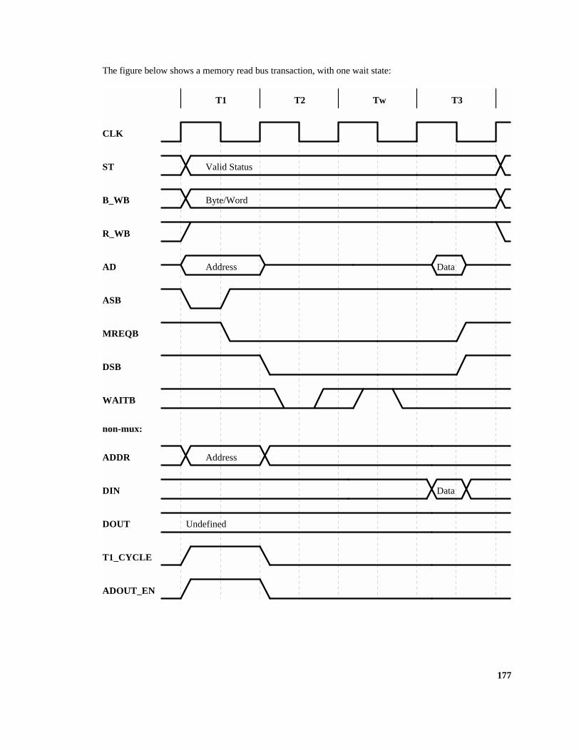
177
The figure below shows a memory read bus transaction, with one wait state:
CLK
AD
ASB
Address
ST
T1 T3T2
WAITB
DSB
MREQB
R_WB
Data
Valid Status
ADDR
DIN
Address
ADOUT_EN
T1_CYCLE
DOUT
Data
non-mux:
Undefined
Tw
B_WB Byte/Word

178
The figure below shows a memory write bus transaction, with one wait state:
CLK
AD
ASB
Address
ST
T1 T3T2
WAITB
DSB
MREQB
R_WB
Data
Valid Status
ADDR
DIN
Address
ADOUT_EN
T1_CYCLE
DOUT Data
non-mux:
(ignored)
Tw
B_WB Byte/Word

179
The figure below shows an I/O read bus transaction, with only the automatic wait state:
Note that the timing for the falling edge of Data Strobe for an I/O bus transaction is different form the corre-sponding timing for a Memory Read bus transaction.
CLK
AD
ASB
Address
ST
T1 T3T2
WAITB
DSB
MREQB
R_WB
Data
Valid Status
ADDR
DIN
Address
ADOUT_EN
T1_CYCLE
DOUT
Data
non-mux:
Undefined
Twa
B_WB Byte/Word
(inactive)

180
The figure below shows an I/O write bus transaction, with only the automatic wait state:
CLK
AD
ASB
Address
ST
T1 T3T2
WAITB
DSB
MREQB
R_WB
Data
Valid Status
ADDR
DIN
Address
ADOUT_EN
T1_CYCLE
DOUT Data
non-mux:
(ignored)
Twa
B_WB Byte/Word
(inactive)

181
The figure below shows an I/O read bus transaction, with one additional wait state:
CLK
AD
ASB
Address
ST
T1 T3T2
WAITB
DSB
MREQB
R_WB
Data
Valid Status
ADDR
DIN
Address
ADOUT_EN
T1_CYCLE
DOUT
Data
non-mux:
Undefined
Twa Tw
B_WB Byte/Word
(inactive)

182
The figure below shows an I/O write bus transaction, with one additional wait state:
CLK
AD
ASB
Address
ST
T1 T3T2
WAITB
DSB
MREQB
R_WB
Data
Valid Status
ADDR
DIN
Address
ADOUT_EN
T1_CYCLE
DOUT Data
non-mux:
(ignored)
Twa Tw
B_WB Byte/Word
(inactive)

183
The figure below shows an internal operation bus transaction:
Note that the Wait Request input us not sampled for this type of bus transaction.
CLK
AD
ASB
Undefined
ST
T1 T3T2
WAITB
DSB
MREQB
R_WB
0000 (Internal Operation)
ADDR
DIN
Undefined
ADOUT_EN
T1_CYCLE
DOUT
non-mux:
Undefined
(inactive)
(inactive)
B_WB Undefined
(ignored)
(ignored)

184
The figure below shows a refresh bus transaction:
Note that the Wait Request input us not sampled for this type of bus transaction.
This type of bus transaction is also issued in response to a Stop request.
CLK
AD
ASB
Refresh Address
ST
T1 T3T2
WAITB
DSB
MREQB
R_WB
0001 (Refresh)
ADDR
DIN
Refresh Address
ADOUT_EN
T1_CYCLE
DOUT
non-mux:
Undefined
(inactive)
B_WB (same as previous)
(ignored)
(same as previous)
(ignored)

185
The figure below shows an interrupt acknowledge bus transaction:
Note that the Wait Request input is sampled twice during this bus transaction, once before the Data Strobe isactivated and once while Data Strobe is active. Memory write bus transactions follow immediately, to savethe program status.
CLK
AD
ASB
Undefined
ST
T1 TwaTwa
WAITB
DSB
MREQB
R_WB
Valid Status
ADDR
DIN
Undefined
ADOUT_EN
T1_CYCLE
DOUT
non-mux:
Undefined
Twa Twa
B_WB
(inactive)
T2 Twa T3
Identifier
Identifier
T4 T5
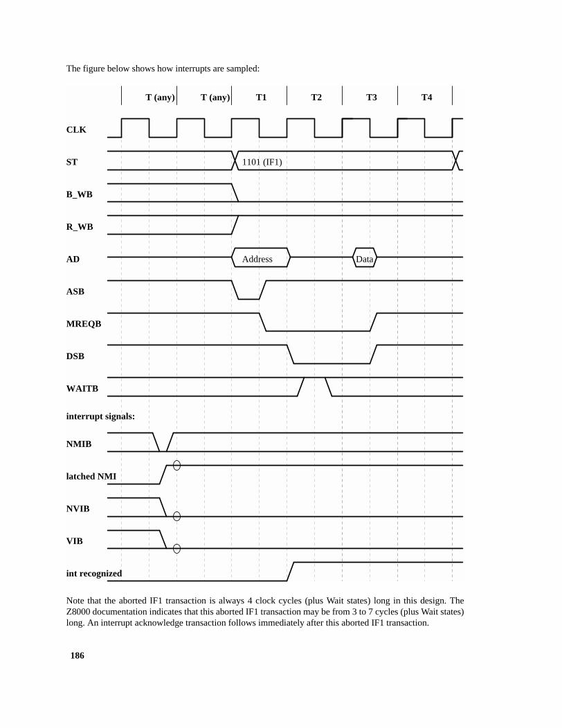
186
The figure below shows how interrupts are sampled:
Note that the aborted IF1 transaction is always 4 clock cycles (plus Wait states) long in this design. TheZ8000 documentation indicates that this aborted IF1 transaction may be from 3 to 7 cycles (plus Wait states)long. An interrupt acknowledge transaction follows immediately after this aborted IF1 transaction.
CLK
AD
ASB
Address
ST
T (any) T2T (any)
WAITB
DSB
MREQB
R_WB
1101 (IF1)
NMIB
latched NMI
int recognized
VIB
NVIB
interrupt signals:
T1
B_WB
T3 T4
Data

187
The figure below shows the sampling of Bus Request and the entry into the Bus Acknowledge state:
Processor operation stops completely while Bus Acknowledge is active, even though it is theoretically pos-sible for some internal operations to continue in parallel. This is believed to be consistent with the operationof the Z8000 processor.
CLK
AD (read)
MREQB
Address
ST
T (any) T3T1
DSB (read)
ASB
R_WB
BUSREQB
internal req
DSB (write)
BUSACKB
bus request signals
T2
B_WB
Tx Tx
AddressAD (write)

188
The figure below shows the sampling of Bus Request and the exit from the Bus Acknowledge state:
The first two clock cycles after exiting the Bus Acknowledge state are still part of the Bus Acknowledgesequence, and no processing takes place during these clock cycles. Processor operation resumes where it leftoff upon entering the Bus Acknowledge state. This may or may not be the start of another bus transaction.
Note that the Bus Request input must remain inactive (High) for at least two clock cycles between succes-sive bus requests. This is consistent with the operation of the Z8000 processor and is a consequence of thetwo clock cycles required for recovery at the end of a Bus Acknowledge sequence.
CLK
AD
MREQB
Address
ST
Tx TxTx
DSB
ASB
R_WB
BUSREQB
internal req
BUSACKB
bus request signals
Tx
B_WB
Tresume
Same as previous cycle
Same as previous cycle
Same as previous cycle

189
The figure below shows how the Stop Request is sampled:
Note that the Stop Request input is sampled prior to an IF1 bus transaction or a Stop bus transaction only.The IF1 bus transaction that follows the sampling of Stop Request active is always three clock cycles long,even if the IF1 bus transaction for the fetched instruction would normally be four or more clock cycles long.In this case the extra IF1 clock cycles follow the inserted Stop bus transactions.
The diagram above shows two inserted Stop transactions.
CLK
AD
ASB
Address
ST
T (any) T3T1
WAITB
DSB
MREQB
R_WB
1101 (IF1)
STOPB
latched Stop
stop signals:
T2
B_WB
T1 T2
Data
T3 T1
0001 (Refresh)
Address Address
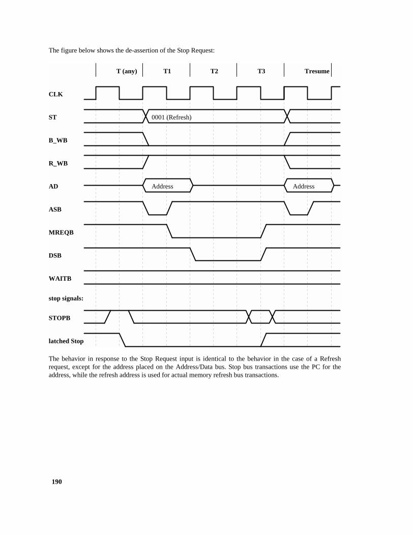
190
The figure below shows the de-assertion of the Stop Request:
The behavior in response to the Stop Request input is identical to the behavior in the case of a Refreshrequest, except for the address placed on the Address/Data bus. Stop bus transactions use the PC for theaddress, while the refresh address is used for actual memory refresh bus transactions.
CLK
AD
ASB
Address
ST
T (any) T3T1
WAITB
DSB
MREQB
R_WB
STOPB
latched Stop
stop signals:
T2
B_WB
Tresume
0001 (Refresh)
Address

191
The figure below shows the first of three cases of the Trap timing:
The instruction fetched during the IF1 bus transaction is pushed as the identifier for this trap. The wordfetched during the IFn bus transaction is ignored. The Program Counter does not increment beyond PC + 2,and this is the value pushed on the stack.
CLK
AD
ASB
PC
ST
T1 T1T2
WAITB
DSB
MREQB
R_WB
1101 (IF1)
ADDR
DIN
PC
ADOUT_EN
T1_CYCLE
DOUT
non-mux:
Undefined
T3 T4
B_WB
T2 T3
PC + 2
1100 (IFn)
PC + 2

192
The figure below shows the second of three cases of the Trap timing:
This case occurs when bits 15:14 of the fetched instruction are 01. The instruction fetched during the IF1 bustransaction is pushed as the identifier for this trap and the word fetched during the IFn bus transaction isignored. The Program Counter does not increment beyond PC + 2, and this is the value pushed on the stack.
CLK
AD
ASB
PC
ST
T1 T2T2
WAITB
DSB
MREQB
R_WB
1101 (IF1)
ADDR
DIN
PC
ADOUT_EN
T1_CYCLE
DOUT
non-mux:
Undefined
T3 T1
B_WB
T3 T4
PC + 2
1100 (IFn)
PC + 2

193
The figure below shows the third of three cases of the Trap timing:
This is the case used by the System Call instruction, plus a number of illegal instructions. The timing for allof the different cases of a trap are identical, and only the signals during cycles 4-7 of the sequences are dif-ferent.
CLK
AD
ASB
PC
ST
T1 T5T2
WAITB
DSB
MREQB
R_WB
1101 (IF1)
ADDR
DIN
PC
ADOUT_EN
T1_CYCLE
DOUT
non-mux:
Undefined
T3 T4
B_WB
T6 T7

194
The figure below shows the status saving sequence common to both interrupts and traps:
This status-saving sequence immediately follows the interrupt acknowledge or trap sequence. The stackpointer used is the System SP.
CLK
AD
ASB
SP - 2
ST
T1 T2T2
WAITB
DSB
MREQB
R_WB
1001 (Stack)
ADDR
DIN
ADOUT_EN
T1_CYCLE
DOUT
non-mux:
Ignored
T3 T1
B_WB
T3 T4 T1
Identifier
T2
Save FCW
T3
Save PC SP - 4 SP - 6
SP - 2 SP - 4 SP - 6
Save PC Save FCW Identifier

195
The figure below shows the Program Status Area fetch sequence common to reset, traps and interrupts:
This sequence follows the reset sequence directly. This sequence follows the trap or interrupt sequence afterseven clock cycles of no external operation.
CLK
AD
ASB
PSA Addr
ST
T1 T5T2
WAITB
DSB
MREQB
R_WB
1100 (Program memory)
ADDR
DIN
ADOUT_EN
T1_CYCLE
DOUT
non-mux:
Undefined
T3 T4
B_WB
T1 T2 T3 T4
PSA Addr
PSA Addr PSA Addr

196
The figure below shows the Reset timing and reset sequence:
Note that the Y8002 design requires that the Reset Request input be sampled active by two successive risingedges of the System Clock to be recognized. This is believed to be consistent with the operation of theZ8000 processor.
CLK
AD
ASB
ST
Tx Tr2Tx
WAITB
DSB
MREQB
R_WB
0000 (Internal Operation)
RESETB
internal Reset
Reset signals:
Tx Tr1
B_WB
Tr3 Tr4 Tr5 Tr6
ignored

197
Chapter 7 Interrupts and Traps
The Z8000 architecture supports three different types of interrupts and four different types of trap. One ofthe traps defined in the architecture (segmentation) is not present in either the Z8002 processor or in theY8002 design and will not be discussed. In addition, the Y8002 design extends the operation of one of thetraps. Each interrupt and trap type will be discussed below. The detailed timing for interrupts and traps wasshown in the previous chapter.
The response to an interrupt or trap is nearly identical, the difference being the interrupt acknowledge buscycle generated in response to an interrupt. The interrupt acknowledge cycle samples the data bus and thedata is used as an identifier for the interrupt. A trap uses the first word of the instruction that causes the trapas the identifier.
After the interrupt acknowledge cycle (in the case of an interrupt), or the fetch of the offending instruction(in the case of a trap) the processor pushes the Program Counter, followed by the FCW, followed by an iden-tifier, onto the system stack. The new FCW and Program Counter are then fetched from the Program StatusArea in program memory to start the service routine. At the end of the service routine an IRET instruction isused to restore the operating state of the processor. The PC value pushed in various cases is shown below:
The start of the Program Status Area is pointed to by the PSAP register in the processor. This register iscleared by a Reset and should be written with a different value using a LDCTL instruction before the Pro-gram Status Area is accessed. The Program Status Area starts on a 256-byte boundary and is organized asshown in the table below:
Exception Pushed PC value
EPU instruction trapAddress of second word of EPU instruction (all EPU instruc-tions are two words)
Privileged Instruction TrapAddress of second word of privileged instruction (all privi-leged instructions are two words).
System Call/Unimplemented Instruction Trap
Address of word following offending instruction word (next instruction for one-word instructions, second word of instruc-tion for two-word instructions)
Any InterruptAddress of next instruction (current instruction if block instruction that has not completed is interrupted)

198
The Program Status Area should be relocated from its reset location because the Reset FCW and PC arefetched from locations 0x0002 and 0x0004 respectively, which interferes with the Program Status Areaentry for the Extended Instruction Trap when using the first 256-byte page as the Program Status Area. Thetwo reserved locations at the start of the Program Status Area hint that the Z8000 architecture intended themto be used for Reset, but that there was an error in the original Z8000 implementation. The Y8002 matchesthe behavior of the Z8002 design.
An Extended Instruction Trap occurs when the processor fetches an Extended Instruction while the EPA bitin the FCW is cleared, indicating that no EPU is present in the system. This allows the processor to emulatethe operation of the Extended Instruction in software. In those versions of the Y8002 design where theExtended Instructions are not implemented this trap will never occur, as the Unimplemented InstructionTrap takes precedence.
The Privileged Instruction Trap occurs when the processor fetches a privileged instruction while the SYS bitin the FCW is cleared, indicating the processor is operating in Normal mode. This prevents Normal mode
Offset from PSAP Contents Interrupt/Trap type
0x000 Reserved
0x002 Reserved
0x004 FCW Extended Instruction Trap0x006 PC
0x008 FCW Privileged Instruction Trap
0x00A PC0x00C FCW SC and Unimplemented Instruction Trap
0x00E PC
0x010 Not used0x012
0x014 FCW Non-maskable Interrupt
0x016 PC0x018 FCW Non-vectored Interrupt
0x01A PC
0x01C FCW Vectored Interrupts0x01E PC (vector = 0x00)
0x020 PC (vector = 0x01)
0x022 PC (vector = 0x02). .
. .
. .0x21A PC (vector = 0xFE)
0x21C PC (vector = 0xFF)

199
programs from affecting system resources such as I/O. In those versions of the Y8002 design where the Sys-tem/Normal mode operation is not implemented this trap will never occur.
The SC and Unimplemented Instruction Trap operation is an extension of the original Z8002 processor’s SCInstruction Trap. In addition to being triggered by the SC opcode, any opcode that is not implemented in theY8002 design will also trigger this trap. Because the first word of the offending opcode is pushed onto thesystem stack as the trap identifier, these cases can always be distinguished in software. This enhanced oper-ation makes the Y8002 design more robust by defining the operation of the processor for any opcode combi-nation. Note that an illegal field encoding in a valid instruction, for example when selecting double orquadruple registers, does not trigger any kind of trap.
The Non-maskable Interrupt is triggered by a falling edge on the Non-maskable Interrupt Request input.This interrupt request really is edge-triggered and cannot be disabled by software.
The Non-vectored Interrupt is taken when the Non-vectored Interrupt Request input is asserted and theNVIE bit in the FCW is set. Clearing the NVIE bit in the FCW disables non-vectored interrupts. Note thatthe Non-vectored Interrupt Request input must remain asserted until the corresponding interrupt acknowl-edge bus cycle is issued by the processor. This interrupt is called non-vectored because even though an iden-tifier is read during the interrupt acknowledge cycle, it is not used by the processor and is merely pushedonto the system stack for use by software.
The Vectored Interrupt is taken when the Vectored Interrupt Request input is asserted and the VIE bit in theFCW is set. Clearing the VIE bit in the FCW disables vectored interrupts. The Vectored Interrupt Requestinput must also remain asserted until asserted until acknowledged by the processor. This interrupt is calledvectored because the processor uses the data returned from the interrupting device during the interruptacknowledge cycle (the “vector”) to select from a number of new PC values stored in the Program StatusArea. Only the lower eight bits of the vector are used for this purpose, selecting from among 256 differentPC values. All vectored interrupts share the same FCW value in the Program Status Area.
In the case of a simultaneous trap and interrupt or multiple interrupt requests the following prioritizationapplies. Once the highest priority request has been answered, the new FCW and PC applies and the remain-ing pending interrupt requests are accepted as appropriate.
Priority Interrupt or trap type
Highest Traps. Note that only one type of trap can occur at a time.
Non-maskable Interrupt
Vectored InterruptLowest Non-vectored Interrupt

200

201
Chapter 8 Reset
The Device Reset input forces the Y8002 processor into a known state, irrespective of its current state. Thisinput must be sampled active for at least two successive rising edges of the clock input to be properly recog-nized, and then on the next falling edge of the clock all processor outputs assume known states. This statecontinues as long as the Device Reset input remains active. The reset state of all processor outputs is shownin the table below:
Once the Device Reset input is sampled inactive the processor fetches an FCW and PC value from memorylocations 0x0002 and 0x004 respectively. Both of these locations are in the program memory address spaceand the processor is in System mode for these fetches. Execution then begins at the address of the fetchedPC with the status from the fetched FCW.
The Device Reset does not affect any of the registers in the register file. In fact the only register that is ini-tialized during the reset state is the Program Status Area Pointer, which is cleared to all zeros. As mentionedpreviously, the PSAP should be reprogrammed to point elsewhere in memory to avoid a conflict between thereset locations of 0x0002 and 0x0004 and the Program Status Area entry for the Extended Instruction trap.
Name Description Reset state
AD[15:0] Address/Data Bus 3-state
ADDR[15:0] Address Bus Previous value (unaffected by reset).ADOUT_EN Address Output Enable Low (inactive).
ASB Address Strobe High (inactive).
B_WB Byte/Word Low (signalling Word).BUSACKB Bus Acknowledge High (inactive).
DOUT Data Output Previous value (unaffected by reset).
DSB Data Strobe High (inactive).MOB Multi-micro Out High (inactive).
MREQB Memory Request High (inactive).
N_SB Normal/System Low (signalling System).R_WB Read/Write High (signalling Read).
ST[3:0] Status All zero (signalling internal operation).
T1_CYCLE T1 Cycle Identifier Low (inactive).

202
If the Bus Request input is active upon exiting the reset state the fetch of the FCW will occur before the busis released by the processor. This is because the Bus Request input is sampled at the start of a bus transac-tion.
If the Stop Request input is active upon exiting the reset state both the FCW and PC will be fetched, as willthe first word of the first instruction, before any stop transactions are inserted. Again, this is consistent withthe way that the Stop Request input is sampled at the start of an IF1 bus transaction.

203
Chapter 9 Verilog HDL Source
This chapter presents an overview of the Verilog HDL source code for the Y8002 design sufficient to under-stand the basic organization and operation of the design. Also described are the options available for thedesign. No attempt will be made to describe the internal operation of the design in detail. Refer to the com-ments embedded in the source code for that type of information. The test bench, described in a separatechapter, is covered in much more detail because the user may actually find it useful to modify the test bench.
The design can be viewed from two different standpoints. First is the organization of the design files them-selves. Second is the logical organization of the Verilog HDL modules contained in the files. Both of theseviews are shown in the table below.
Each file contains just one Verilog HDL module, and may include (using the ‘include directive) one or moreother files. In all cases the name of the file is identical to the name of the Verilog HDL module that it con-tains. The only files that do not contain a Verilog HDL module are defines.v, which contains all of the‘define statements for the design in one central location, and version.v, which selects the options for thedesign.
Before discussing individual Verilog HDL modules, it is appropriate to describe the versions of the designthat are available. These versions are controlled by ‘define statements in the file version.v. This file is refer-enced by an ‘include statement in the top level of the design.
The first ‘define selects between an ASIC option and an FPGA option. The primary difference betweenthese two options is that the FPGA option does not include any 3-state function for those outputs that arenormally able to go high-impedance. If this functionality is required it can be implemented outside of thedesign. This option is available because synthesis tools often have difficulty implementing 3-state signals.
file organization logical organizationy8002.v y8002.v
version.v core8002.vcore8002.v ext_int.v
defines.v machine.v
ff_byte.v control.vff_word.v datapath.v
reg_word.v reg_word.v
ext_int.v reg_file.vmachine.v ff_byte.v
control.v ff_word.v
datapath.v

204
The second ‘define selects between the normal multiplexed option and a special non-multiplexed option.The multiplexed option employs the normal bidirectional Address/Data bus familiar to Z8002 users, whilethe non-multiplexed option uses separate Address, Data In and Data Out busses. The multiplexed optionobviously employs 3-state drivers, so selecting this option in conjunction with the FPGA option doesn’tmake a lot of sense.
The top level design file (and module) is called y8002.v. This file is the top level “wrapper” for the designand is where the design options are implemented. It is also where the user can implement technology-spe-cific I/O cells or buffers. Several heavily-loaded signals from the core design are buffered here using instan-tiated ACTEL-specific cells in the FPGA option. These cells can obviously be replaced with differentbuffers for different FPGA vendors. Technology-specific buffers for these heavily-loaded signals can alsobe instantiated in the ASIC option. This level is also where the user can insert I/O cells if desired.
The core8002.v module contains essentially all of the design, but no logic is actually implemented at thislevel. Rather, all of the remaining design files are referenced here, using ‘include statements, and the fourmain modules are instantiated. The heavily-loaded signals exit this module and then are input to the modulewith a slightly different name to allow for technology-specific buffers to be implemented. These signals arethe synchronized reset signal (resetpls_reg out and resetb in), the instruction register (inst_reg out andbuf_inst_reg in), and the signal which stops all of the state machines for Bus Request, Wait Request andStop Request (hold_mach out and buf_hold_mach in). The clock input to this module is called buf_CLK,having been buffered outside of the module. As mentioned previously, nearly all of the logic in the design isclocked by the rising edge of this clock. The only exceptions are in the external interface where certain fall-ing-edge operation are required for compatibility with the Z8002 device.
The file defines.v contains all of the encoding for multi-bit control fields and state machines. Most of thesecontrol field encoding can be changed to attempt to minimize logic, subject to restrictions listed in the file.However, the current encoding should be close to optimal, given our experience with synthesis tools, so theuser is strongly cautioned against any such changes. The main state machines in the design are one-hotencoded. This type of encoding works well even in ASIC implementations because the control fields are notthat wide. One-hot encoding also leads to fewer levels of logic and hence higher operating frequency in mostcases.
The ff_byte.v and ff_word.v modules contain a byte-wide register and a word-wide register respectively, foruse in the register file. These registers are not affected by reset.
The reg_word.v module contains a word-wide register for use in the datapath. This register is cleared to allzeros by reset and is used for temporary storage in the datapath.
The reg_file.v module contains the Y8002 register file and is instantiated in the datapath. The register file isimplemented using standard flip-flops rather than latches or RAM because of its relatively small size. This isalso leads to a more robust and technology-independent design.
The ext_int.v module contains the external inteface for the Y8002 processor. This is where all of the externalcontrol signals are generated with the proper timing, and all inputs are sampled with the proper timing. Thismodule contains a mixture of rising-edge triggered logic and falling-edge triggered logic as required forcompatible timing. Most outputs from this module come directly from the outputs of flip-flops, but wherethis is not possible, the design guarantees glitch-free operation.
The machine.v module contains the five main state machines for the device. The primary state machine iscalled mach_cyc and this state machine controls everything in the design. The four auxiliary state machinesare controlled by the primary state machine and run only in specific circumstances. The mltl_cyc statemachine runs to perform the multiply algorithm during MULT and MULTL instructions. The divl_cyc state

205
machine runs to perform the divide algorithm during DIV and DIVL instructions. The rti_cyc state machineruns as part of the reset sequence, the trap sequence and the interrupt sequence to fetch data from the Pro-gram Status Area. The trap_cyc state machine runs during the trap sequence and the interrupt sequence toperform the state-saving operation that writes the FCW, PC and an identifier to the stack.
The control.v module generates all of the control signals used throughout the design. This module containsonly combinatorial logic. This partitioning allows this module to be replaced with a PLA or similar structurein an ASIC implementation. Modern synthesis tools have made this option less attractive than it once was,but the option is still available with this partitioning. Multi-bit control signals are generated using the mne-monics defined in the file defines.v to increase the readability of this module.
The datapath.v module contains all of the data manipulation logic for the design. This includes the ALU, theregister file, the PC and FCW, the PSAP and the instruction register. This module drives the internal bus,called intrnl_bus, which carries all data and addresses in the design. The design uses a classical 16-bit ALU,without any special ALU logic for the multiply and divide operations. Three small state machines areincluded in this module. Two are used for the LDM instruction, to count the number of transfers and to gen-erate the register address. The third is used to count the iterations for the multiply and divide operations.
For more detailed information about the design refer to the comments embedded in the Verilog HDL sourcecode.

206

207
Chapter 10 Test Bench
This chapter covers the operation of the test bench included with the design. The test bench instantiates theprocessor, and using a series of test patterns, verifies the operation of the processor. The included test pat-terns exercise every instruction and completely verify the operation of all of the flags. Also tested are all ofthe opcodes that cause an illegal instruction trap. The test bench normally runs without any Wait states, BusRequests, or Stop Requests. However, each of these external stimuli, alone or in combination, can be gener-ated by the test bench.
The overall operation of the test bench is controlled by a set of ‘define statements at the top of the test benchfile. These high-level options will be discussed first, followed by a section-by-section description of theoperation of the test bench. Much of this discussion will make more sense if a copy of the test bench is avail-able, but the general operation can be deduced without the actual Verilog HDL code at hand.
The first ‘define selects the type of memory used by the test bench. Normal test bench operation uses twoseparate memories, one for reading (and it really is read-only) and another that holds compare data for anywrites that the processor will be performing. Each test pattern loads both of these memories before starting,and the test bench checks every write operation performed by the processor against the compare memorycontents at that address. In this regard the test bench operates much like a piece of Automatic Test Equip-ment (ATE). The alternative is a uniform memory that is read and written by the processor. This optionallows user code to be loaded into the test bench memory for simulation.
The second ‘define selects the clock cycle time for the simulation. This option is essentially meaninglesswhen simulating the Verilog HDL source code, but will be useful if the test bench is used with a gate-levelimplementation of the design, as well as when generating trace files to use on a tester in the case of an ASICimplementation.
The third ‘define enables or disables the option of generating a trace file that can be converted into theproper format for a tester. The trace file is generated in a print-on-change format and includes the directioncontrol signal for the address/data bus. All input stimuli are generated assuming that the tester uses the NRZformat for all signals and that there are two tester cycles per each processor clock cycle.
The fourth ‘define controls the insertion of Wait states by the test bench. This is a global enable, used toselect zero, one or two wait states for each and every transaction that samples the WAITB input. Finer con-trol, by each transaction type is also available. This will be discussed in the corresponding section descrip-tion below.
The fifth ‘define controls the insertion of Bus Requests. Only a global enable is available, with a number ofoptions as to the length of each bus request. When enabled, a Bus Request is generated between every bustransaction. The test bench is not capable of verifying proper operation of the Bus Request except via aproper cycle count for the pattern.

208
The sixth ‘define is also used with Bus Requests. It selects the inactive time for the Bus Request. The proces-sor requires that BUSREQB be inactive for at least two clock cycles between requests, and this is the mini-mum allowed by this ‘define. To verify proper functionality, longer inactive times may also be selected here.
The final ‘define controls the insertion of Stop Requests. Only a global enable is available, with a number ofoptions as to the number of Stop Requests in a burst. When enabled, a Stop Request is generated for everyinstruction (recall that Stop Requests are only accepted between instructions). The test bench is not capableof verifying the proper operation of the Stop Request except via a proper cycle count for the pattern.
The remainder of this chapter will discuss each section of the Verilog HDL code of the test bench. Each sec-tion is identified by a comment block that will be referenced here.
set test cycle time
This section uses the clock cycle time selected by the top level ‘define to set two parameters to create theproper timing in the test bench. Both the memory access time and the minor cycle time are set here. Theminor cycle time will be explained in the relevant section below.
select wait patterns
This section uses the number of wait states selected by the corresponding top level ‘define to create theactual data patterns which drive the WAITB input. Separate data patterns are available for each transactiontype. The data patterns correspond, msb-to-lsb, to the inverse of the value applied to the WAITB startingwith the T1 clock cycle of the transaction. One bit is used for each clock cycle, and WAITB can be assertedmore than once per bus transaction. This is useful in the case of interrupt acknowledge cycles, whereWAITB is sampled at two separate places in the transaction.
select busreq operation
This section uses the Bus Request options selected by the two top level ‘define statements to set three param-eters used by the state machine that generates the BUSREQB input. The operation of the bus request statemachine will by covered in the relevant section below.
select stop operation
This section uses the Stop Request option selected by the top level ‘define statement to set two parametersused by the state machine that generates the STOPB input. The operation of the stop request state machinewill by covered in the relevant section below.
instantiate processor
This is the section where the processor is actually instantiated into the test bench. All of the pin variables arealso declared here. Recall that there are actually two versions of the processor available, multiplexed andnon-multiplexed, selected in the file version.v. This section automatically recognizes the version and con-nects the correct one.
program memory and write compare data
This section contains the program memory and, if necessary, the memory that holds the compare data. Bothmemories support both byte and word accesses. This is actually done in the memory interface section below.
test bench internal variables

209
This section declares all of the variables for the test bench. Most of the variables are self-explanatory. How-ever, note that there are actually two variables per input pin. The test bench version has an extension _varand is the one that is manipulated by the test bench without regard to the actual timing of when the input isapplied to the processor. The actual pin variable takes its value from the test bench version at the appropriatetime during each clock cycle.
generate the overall test bench timing
This section contains the main timing generator for the test bench. All test bench variables are initialized andthe timing generator is started here. The test bench timing generator consists of a ten bit shift register, withoutputs called TREF0 through TREF9. The minor cycle time is the period of the “clock” for this statemachine. Only one of these outputs is active at a time, and rising edges on these signals are used to drivestate machines and generate the actual timing for the input signals. Each cycle of this timing generator corre-sponds to one tester cycle and one-half of a processor clock cycle.
This section also contains a cycle counter that counts the clock cycles for a pattern. This count is not used foranything in the test bench but is provided as a convenience for anyone running the test bench. Recall that thetest bench cannot verify proper operation with Wait states, Bus Requests or Stop Requests except for theproper cycle count upon pattern completion.
The end-of-pattern condition is also recognized in this section. The test bench recognizes the end of a testpattern when an address of FFFEh is sampled by the ASB signal.
peripheral simulation tasks are in a separate file
TREF0
TREF1
TREF2
TREF3
TREF4
TREF5
TREF6
TREF7
TREF8
TREF9

210
This short section uses an ‘include to bring in a file that contains a number of tasks used by the test bench.There is a reset task and a task to run each test pattern. Each test pattern task initializes the error counter,resets the processor and loads the memories with the test program and compare data. It also loads the inter-rupt generator memory, if required by the test pattern.
t-cycle tracker to generate inputs
This section contains the state machine that tracks the t-state (the clock cycle within a machine cycle) of theprocessor, by synchronizing with the ASB signal. This synchronization is necessary to assert the variousprocessor inputs at the correct time. This section also decodes the Status lines to select the proper pattern forthe Wait State generator.
busreq generator state machine
The bus request state machine uses the parameters selected earlier and the state of the BUSACKB pin tosequence through the states necessary to generate the requested on and off times for the Bus Request. Thisstate machine is clocked by the rising edge of TREF4 when the CLK input is High. The BUSREQB signal isthe logical AND of the two most-significant bits of the bus request state machine.
stop generator state machine
The stop request state machine uses the parameters selected earlier to sequence through the states necessaryto generate a Stop Request at the correct time. This state machine is clocked by the rising edge of TREF4when the ASB output is Low (in other words, at the start of every machine cycle). The STOPB signal is thelogical AND of the two most-significant bits of the stop request state machine.
interrupt generator state machine
The interrupt request state machine uses information loaded into the interrupt generator memory at the startof each test pattern to generate interrupts during the test pattern. Every interrupt acknowledge transactionincrements the address used to access the interrupt generator memory. One consequence of this is that if twointerrupts are generated by an entry, there must be a subsequent dummy entry to account for the secondinterrupt acknowledge transaction. Similarly, if three interrupts are generated by an entry, two subsequentdummy entries are required.
Each entry in the interrupt generator memory contains one bit for each interrupt type, a four bit transactioncount, a four bit transaction status and a sixteen bit address. The interrupt request state machine contains acounter that is reset by an interrupt acknowledge transaction and then increments each time that a transactionmatching the address and status is recognized. When the transaction count, transaction status and address allmatch those in the interrupt generator memory, the selected interrupt is generated at the correct time duringthe transaction.
Bit position(s) Width Meaning26 1 Value for NMIB
25 1 Value for NVIB
24 1 Value for VIB23:20 4 Count
19:16 4 Transaction Status
15:0 16 Transaction Address

211
Once asserted, the VIB and NVIB interrupt requests remain active until the test bench recognizes the corre-sponding interrupt acknowledge transaction. The NMIB interrupt request is different, however. In the caseof NMIB, the request is a pulse that is only one-half of a clock cycle wide. This is to verify the edge-trig-gered operation on this input to the processor.
Every test pattern except for the one which actually tests the interrupts (called int_ops) merely loads a nullvalue into the interrupt generator memory.
processor inputs
This section adds the final timing to the test bench variables to create the actual processor inputs. The CLKinput changes on the rising edge of TREF5, and all of the other inputs change on the rising edge of TREF3.In the case of BUSREQB, NVIB, RESETB, and VIB it is the rising edge of TREF3 just before a rising edgeof CLK. In the case of NMIB, STOPB and WAITB it is the rising edge of TREF3 just before a falling edgeof CLK. Note that the NVIB, RESETB and VIB inputs persist. That is, the value is latched by the test benchand persists until the corresponding test bench variable is de-asserted. In all other cases the input is actuallydriven for only half of a clock cycle and is then returned to the inactive state. The test bench does this toguarantee that the processor input is actually sampled on the correct CLK edge.
memory interface
This section connects the test bench memories to the processor. The address/data bus is latched by the risingedge of TREF4 during the ASB Low time. Input data is applied to the processor on the rising edge of TREF2during the CLK Low time (after the memory access time specified previously). The memory interfaces sup-port both byte and word transfers properly.
trace file generation
This section generates the print-on-change trace file, if that option is selected. The complete test programrequires slightly more than 110,000 clock cycles to complete. If the tester pattern memory is not deepenough for the entire set of patterns, individual patterns can be enabled or disabled in the next section bycommenting out the appropriate task.
load and execute the test patterns
This final section is where the actual test pattern tasks are run. Note that they can be individually commentedout if required. The existing pattern sequence is arbitrary, and the patterns can actually be run in any order.Even though each pattern task does a hardware reset, there is an initial reset task to force all processor out-puts to be known. This should always be the first task to run for this reason. Below is a list of the test pat-terns and their functionality:
Pattern Name Pattern Number Coveragedat_ops 0 data movement instructions
alu_ops 1 arithmetic and logical instructions
jmp_ops 2 jumps, calls, and returnbit_ops 3 bit operation instructions
lng_ops 4 multiply, divide and multi-bit shifts
blk_ops 5 block-type instructionstrp_ops 6 all opcodes which are supposed to trap
int_ops 7 interrupts

212

213
Appendix 1 Execution details
This Appendix lists the details of the instruction timing. The external sequence shows the length of each buscycle performed as part of the instruction, while the internal sequence shows the actual internal sequence.Refer to the design documentation for more details about the internal sequenceMultiply and divide areshown separately at the end.
Instruction Cycles External Sequence Internal Sequence
ADC Rd, Rs 5 5 3, 2
ADCB Rbd, Rbs 5 5 3, 2
ADD Rd, Rs 4 4 3, 1ADDB Rbd, Rbs 4 4 3, 1
ADDL RRd, RRs 8 8 3, 5
ADD Rd, #data 7 4, 3 3, 1, 3ADDB Rbd, #data 7 4, 3 3, 1, 3
ADDL RRd, #data 14 4, 3, 7 3, 1, 3, 3, 4
ADD Rd, @Rs 7 4, 3 3, 1, 3ADDB Rbd, @Rs 7 4, 3 3, 1, 3
ADDL RRd, @Rs 14 4, 3, 7 3, 1, 3, 3, 4
ADD Rd, address 9 3, 3, 3 3, 3, 3ADDB Rbd, address 9 3, 3, 3 3, 3, 3
ADDL RRd, address 15 3, 3, 3, 6 3, 3, 3, 3, 3
ADD Rd, addr(Rs) 10 3, 4, 3 3, 3, 1, 3ADDB Rbd, addr(Rs) 10 3, 4, 3 3, 3, 1, 3
ADDL RRd, addr(Rs) 16 3, 4, 3, 6 3, 3, 1, 3, 3, 3
AND Rd, Rs 4 4 3, 1ANDB Rbd, Rbs 4 4 3, 1
AND Rd, #data 7 4, 3 3, 1, 3
ANDB Rbd, #data 7 4, 3 3, 1, 3AND Rd, @Rs 7 4, 3 3, 1, 3
ANDB Rbd, @Rs 7 4, 3 3, 1, 3
AND Rd, address 9 3, 3, 3 3, 3, 3ANDB Rbd, address 9 3, 3, 3 3, 3, 3
AND Rd, addr(Rs) 10 3, 4, 3 3, 3, 1, 3
ANDB Rbd, addr(Rs) 10 3, 4, 3 3, 3, 1, 3

214
Instruction Cycles External Sequence Internal Sequence
BIT Rd, #b 4 4 3, 1
BITB Rbd, #b 4 4 3, 1BIT @Rd, #b 8 4, 4 3, 1, 3, 1
BITB @Rd, #b 8 4, 4 3, 1, 3, 1
BIT address, #b 10 3, 3, 4 3, 3, 3, 1BITB address, #b 10 3, 3, 4 3, 3, 3, 1
BIT addr(Rd), #b 11 3, 4, 4 3, 3, 1, 3, 1
BITB addr(Rd), #b 11 3, 4, 4 3, 3, 1, 3, 1
BIT Rd, Rs 10 4, 6 3, 1, 3, 3BITB Rbd, Rs 10 4, 6 3, 1, 3, 3
CALL @Rd 10 4, 3, 3 3, 1, 3, 3
CALL address 12 3, 5, 4 3, 3, 2, 3, 1CALL addr(Rd) 13 3, 6, 4 3, 3, 3, 3, 1
CALR address 10 6, 4 3, 3, 3, 1
CLR Rd 7 7 3, 4CLRB Rbd 7 7 3, 4
CLR @Rd 8 5, 3 3, 2, 3
CLRB @Rd 8 5, 3 3, 2, 3CLR address 11 3, 5, 3 3, 3, 2, 3
CLRB address 11 3, 5, 3 3, 3, 2, 3
CLR addr(Rd) 12 3, 6, 3 3, 3, 3, 3CLRB addr(Rd) 12 3, 6, 3 3, 3, 3, 3
COM Rd 7 7 3, 4
COMB Rbd 7 7 3, 4COM @Rd 12 5, 4, 3 3, 2, 3, 1, 3
COMB @Rd 12 5, 4, 3 3, 2, 3, 1, 3
COM address 15 3, 5, 4, 3 3, 3, 2, 3, 1, 3COMB address 15 3, 5, 4, 3 3, 3, 2, 3, 1, 3
COM addr(Rd) 16 3, 6, 4, 3 3, 3, 3, 3, 1, 3
COMB addr(Rd) 16 3, 6, 4, 3 3, 3, 3, 3, 1, 3COMFLG flag 7 7 3, 4
CP Rd, Rs 4 4 3, 1
CPB Rbd, Rbs 4 4 3, 1CPL RRd, RRs 8 8 3, 5
CP Rd, #data 7 4, 3 3, 1, 3
CPB Rbd, #data 7 4, 3 3, 1, 3CPL RRd, #data 14 4, 3, 7 3, 1, 3, 3, 4
CP Rd, @Rs 7 4, 3 3, 1, 3
CPB Rbd, @Rs 7 4, 3 3, 1, 3CPL RRd, @Rs 14 4, 3, 7 3, 1, 3, 3, 4

215
Instruction Cycles External Sequence Internal Sequence
CP Rd, address 9 3, 3, 3 3, 3, 3
CPB Rbd, address 9 3, 3, 3 3, 3, 3CPL RRd, address 15 3, 3, 3, 6 3, 3, 3, 3, 3
CP Rd, addr(Rs) 10 3, 4, 3 3, 3, 1, 3
CPB Rbd, addr(Rs) 10 3, 4, 3 3, 3, 1, 3CPL RRd, addr(Rs) 16 3, 4, 3, 6 3, 3, 1, 3, 3, 3
CP @Rd, #data 11 4, 4, 3 3, 1, 3, 1, 3
CPB @Rd, #data 11 4, 4, 3 3, 1, 3, 1, 3
CP address, #data 14 3, 4, 4, 3 3, 3, 1, 3, 1, 3CPB address, #data 14 3, 4, 4, 3 3, 3, 1, 3, 1, 3
CP addr(Rd), #data 15 3, 4, 5, 3 3, 3, 1, 3, 2, 3
CPB addr(Rd), #data 15 3, 4, 5, 3 3, 3, 1, 3, 2, 3CPD Rd, @Rs, r, cc 20 4, 5, 11 3, 1, 3, 2, 3, 6, 2
CPDB Rbd, @Rs, r, cc 20 4, 5, 11 3, 1, 3, 2, 3, 6, 2
CPDR Rd, @Rs, r, cc 11+9n 4, 5, 9n, 2 3, 1, 3, 2, (3, 6)n, 2CPDRB Rbd, @Rs, r, cc 11+9n 4, 5, 9n, 2 3, 1, 3, 2, (3, 6)n, 2
CPI Rd, @Rs, r, cc 20 4, 5, 11 3, 1, 3, 2, 3, 6, 2
CPIB Rbd, @Rs, r, cc 20 4, 5, 11 3, 1, 3, 2, 3, 6, 2CPIR Rd, @Rs, r, cc 11+9n 4, 5, 9n, 2 3, 1, 3, 2, (3, 6)n, 2
CPIRB Rbd, @Rs, r, cc 11+9n 4, 5, 9n, 2 3, 1, 3, 2, (3, 6)n, 2
CPSD @Rd, @Rs, r, cc 25 4, 5, 5, 11 3, 1, 3, 2, 3, 2, 3, 6, 2CPSDB @Rd, @Rs, r, cc 25 4, 5, 5, 11 3, 1, 3, 2, 3, 2, 3, 6, 2
CPSDR @Rd, @Rs, r, cc 11+14n 4, 5, (5, 9)n, 2 3, 1, 3, 2, (3, 2, 3, 6)n, 2
CPSDRB @Rd, @Rs, r, cc 11+14n 4, 5, (5, 9)n, 2 3, 1, 3, 2, (3, 2, 3, 6)n, 2CPSI @Rd, @Rs, r, cc 25 4, 5, 5, 11 3, 1, 3, 2, 3, 2, 3, 6, 2
CPSIB @Rd, @Rs, r, cc 25 4, 5, 5, 11 3, 1, 3, 2, 3, 2, 3, 6, 2
CPSIR @Rd, @Rs, r, cc 11+14n 4, 5, (5, 9)n, 2 3, 1, 3, 2, (3, 2, 3, 6)n, 2CPSIRB @Rd, @Rs, r, cc 11+14n 4, 5, (5, 9)n, 2 3, 1, 3, 2, (3, 2, 3, 6)n, 2
DAB Rbd 5 5 3, 2
DEC Rd, #n 4 4 3, 1DECB Rbd, #n 4 4 3, 1
DEC @Rd, #n 11 4, 4, 3 3, 1, 3, 1, 3
DECB @Rd, #n 11 4, 4, 3 3, 1, 3, 1, 3DEC address, #n 13 3, 3, 4, 3 3, 3, 3, 1, 3
DECB address, #n 13 3, 3, 4, 3 3, 3, 3, 1, 3
DEC addr(Rd), #n 14 3, 4, 4, 3 3, 3, 1, 3, 1, 3DECB addr(Rd), #n 14 3, 4, 4, 3 3, 3, 1, 3, 1, 3
DI int 7 7 3, 4
DIV RRd, Rs 11/22/92 5, div, 1 3, 2, div, 1DIVL RQd, RRs 14/36/500 5, div, 1 3, 2, div, 1

216
Instruction Cycles External Sequence Internal Sequence
DIV RRd, #data 13/24/94 4, 3, div, 1 3, 1, 3, div, 1
DIVL RQd, #data 19/41/505 4, 3, 3, div, 1 3, 1, 3, 3, div, 1DIV RRd, @Rs 13/24/94 4, 3, div, 1 3, 1, 3, div, 1
DIVL RQd, @Rs 19/41/505 4, 3, 3, div, 1 3, 1, 3, 3, div, 1
DIV RRd, address 15/26/96 3, 3, 3, div, 1 3, 3, 3, div, 1DIVL RQd, address 21/43/507 3, 3, 3, 3, div, 1 3, 3, 3, 3, div, 1
DIV RRd, addr(Rs) 16/27/97 3, 4, 3, div, 1 3, 3, 1, 3, div, 1
DIVL RQd, addr(Rs) 22/44/508 3, 4, 3, 3, div, 1 3, 3, 1, 3, 3, div, 1
DJNZ R, address 11 11 3, 8DBJNZ Rb, address 11 11 3, 8
EI int 7 7 3, 4
EX Rd, Rs 6 6 3, 3EXB Rbd, Rbs 6 6 3, 3
EX Rd, @Rs 12 4, 5, 3 3, 1, 3, 2, 3
EXB Rd, @Rs 12 4, 5, 3 3, 1, 3, 2, 3EX Rd, address 15 3, 4, 5, 3 3, 3, 1, 3, 2, 3
EXB Rbd, address 15 3, 4, 5, 3 3, 3, 1, 3, 2, 3
EX Rd, addr(Rs) 16 3, 5, 5, 3 3, 3, 2, 3, 2, 3EXB Rbd, addr(Rs) 16 3, 5, 5, 3 3, 3, 2, 3, 2, 3
EXTSB Rd 11 11 3, 8
EXTS RRd 11 11 3, 8EXTSL RQd 11 11 3, 8
HALT 8+3n 5, 3, 3n 3, 2, 3, 3n
IN Rd, @Rs 10 6, 4 3, 3, 4INB Rbd, @Rs 10 6, 4 3, 3, 4
IN Rd, port 12 4, 4, 4 3, 1, 3, 1, 4
INB Rbd, port 12 4, 4, 4 3, 1, 3, 1, 4SIN Rd, port 12 4, 4, 4 3, 1, 3, 1, 4
SINB Rbd, port 12 4, 4, 4 3, 1, 3, 1, 4
INC Rd, #n 4 4 3, 1INCB Rbd, #n 4 4 3, 1
INC @Rd, #n 11 4, 4, 3 3, 1, 3, 1, 3
INCB @Rd, #n 11 4, 4, 3 3, 1, 3, 1, 3INC address, #n 13 3, 3, 4, 3 3, 3, 3, 1, 3
INCB address, #n 13 3, 3, 4, 3 3, 3, 3, 1, 3
INC addr(Rd), #n 14 3, 4, 4, 3 3, 3, 1, 3, 1, 3INCB addr(Rd), #n 14 3, 4, 4, 3 3, 3, 1, 3, 1, 3
IND @Rd, @Rs, r 21 4, 5, 5, 7 3, 1, 3, 2, 4, 1, 3, 2, 2
INDB @Rd, @Rs, r 21 4, 5, 5, 7 3, 1, 3, 2, 4, 1, 3, 2, 2SIND @Rd, @Rs, r 21 4, 5, 5, 7 3, 1, 3, 2, 4, 1, 3, 2, 2
SINDB @Rd, @Rs, r 21 4, 5, 5, 7 3, 1, 3, 2, 4, 1, 3, 2, 2

217
Instruction Cycles External Sequence Internal Sequence
INDR @Rd, @Rs, r 11+10n 4, 5, (5, 5)n, 2 3, 1, 3, 2, (4, 1, 3, 2)n, 2
INDRB @Rd, @Rs, r 11+10n 4, 5, (5, 5)n, 2 3, 1, 3, 2, (4, 1, 3, 2)n, 2SINDR @Rd, @Rs, r 11+10n 4, 5, (5, 5)n, 2 3, 1, 3, 2, (4, 1, 3, 2)n, 2
SINDRB @Rd, @Rs, r 11+10n 4, 5, (5, 5)n, 2 3, 1, 3, 2, (4, 1, 3, 2)n, 2
INI @Rd, @Rs, r 21 4, 5, 5, 7 3, 1, 3, 2, 4, 1, 3, 2, 2INIB @Rd, @Rs, r 21 4, 5, 5, 7 3, 1, 3, 2, 4, 1, 3, 2, 2
SINI @Rd, @Rs, r 21 4, 5, 5, 7 3, 1, 3, 2, 4, 1, 3, 2, 2
SINIB @Rd, @Rs, r 21 4, 5, 5, 7 3, 1, 3, 2, 4, 1, 3, 2, 2
INIR @Rd, @Rs, r 11+10n 4, 5, (5, 5)n, 2 3, 1, 3, 2, (4, 1, 3, 2)n, 2INIRB @Rd, @Rs, r 11+10n 4, 5, (5, 5)n, 2 3, 1, 3, 2, (4, 1, 3, 2)n, 2
SINIR @Rd, @Rs, r 11+10n 4, 5, (5, 5)n, 2 3, 1, 3, 2, (4, 1, 3, 2)n, 2
SINIRB @Rd, @Rs, r 11+10n 4, 5, (5, 5)n, 2 3, 1, 3, 2, (4, 1, 3, 2)n, 2IRET 13 6, 3, 4 3, 3, 3, 3, 1
JP cc, @Rd 7 or 10 4, 3, 3 3, 1, 3, 3
JP cc, address 7 3, 4 3, 3, 1JP cc, addr(Rd) 8 3, 5 3, 3, 2
JR cc, address 6 3, 3 3, 3
LD Rd, Rs 3 3 3LDB Rbd, Rbs 3 3 3
LDL RRd, RRs 5 5 3, 2
LD Rd, @Rs 7 4, 3 3, 1, 3LDB Rbd, @Rs 7 4, 3 3, 1, 3
LDL RRd, @Rs 11 4, 3, 4 3, 1, 3, 3, 1
LD Rd, address 9 3, 3, 3 3, 3, 3LDB Rbd, address 9 3, 3, 3 3, 3, 3
LDL RRd, address 12 3, 3, 3, 3 3, 3, 3, 3
LD Rd, addr(Rs) 10 3, 4, 3 3, 3, 1, 3LDB Rbd, addr(Rs) 10 3, 4, 3 3, 3, 1, 3
LDL RRd, addr(Rs) 13 3, 4, 3, 3 3, 3, 1, 3, 3
LD Rd, Rs(#disp) 14 4, 7, 3 3, 1, 3, 4, 3LDB Rbd, Rs(#disp) 14 4, 7, 3 3, 1, 3, 4, 3
LDL RRd, Rs(#disp) 17 4, 7, 3, 3 3, 1, 3, 4, 3, 3
LD Rd, Rs(Rx) 14 4, 7, 3 3, 1, 3, 4, 3LDB Rbd, Rs(Rx) 14 4, 7, 3 3, 1, 3, 4, 3
LDL RRd, Rs(Rx) 17 4, 7, 3, 3 3, 1, 3, 4, 3, 3
LD @Rd, Rs 8 5, 3 3, 2, 3LDB @Rd, Rbs 8 5, 3 3, 2, 3
LDL @Rd, RRs 11 5, 3, 3 3, 2, 3, 3
LD address, Rs 11 3, 5, 3 3, 3, 2, 3LDB address, Rbs 11 3, 5, 3 3, 3, 2, 3
LDL address, RRs 14 3, 5, 3, 3 3, 3, 2, 3, 3

218
Instruction Cycles External Sequence Internal Sequence
LD addr(Rd), Rs 12 3, 6, 3 3, 3, 3, 3
LDB addr(Rd), Rbs 12 3, 6, 3 3, 3, 3, 3LDL addr(Rd), RRs 15 3, 6, 3, 3 3, 3, 3, 3, 3
LD Rd(#disp), Rs 14 4, 7, 3 3, 1, 3, 4, 3
LDB Rd(#disp), Rbs 14 4, 7, 3 3, 1, 3, 4, 3LDL Rd(#disp), RRs 17 4, 7, 3, 3 3, 1, 3, 4, 3, 3
LD Rd(Rx), Rs 14 4, 7, 3 3, 1, 3, 4, 3
LDB Rd(Rx), Rbs 14 4, 7, 3 3, 1, 3, 4, 3
LDL Rd(Rx), RRs 17 4, 7, 3, 3 3, 1, 3, 4, 3, 3LD Rd, #data 7 4, 3 3, 1, 3
LDB Rd, #data 7 4, 3 3, 1, 3
LDB Rbd, #data 5 5 3, 2LDL RRd, #data 11 4, 3, 4 3, 1, 3, 3, 1
LD @Rd, #data 11 4, 4, 3 3, 1, 3, 1, 3
LDB @Rd, #data 11 4, 4, 3 3, 1, 3, 1, 3LD address, #data 14 3, 4, 4, 3 3, 3, 1, 3, 1, 3
LDB address, #data 14 3, 4, 4, 3 3, 3, 1, 3, 1, 3
LD addr(Rd), #data 15 3, 4, 5, 3 3, 3, 1, 3, 2, 3LDB addr(Rd), #data 15 3, 4, 5, 3 3, 3, 1, 3, 2, 3
LDA Rd, address 12 4, 4, 4 3, 1, 3, 1, 3, 1
LDA Rd, addr(Rs) 13 4, 5, 4 3, 1, 3, 2, 3, 1LDA Rd, Rs(#disp) 15 4, 7, 4 3, 1, 3, 4, 3, 1
LDA Rd, Rs(Rx) 15 4, 7, 4 3, 1, 3, 4, 3, 1
LDAR Rd, address 15 4, 7, 4 3, 1, 3, 4, 3, 1LDCTL FCW, Rs 7 7 3, 4
LDCTL REFRESH, Rs 7 7 3, 4
LDCTL PSAP, Rs 7 7 3, 4LDCTL NSP, Rs 7 7 3, 4
LDCTL Rd, FCW 7 7 3, 4
LDCTL Rd, REFRESH 7 7 3, 4LDCTL Rd, PSAP 7 7 3, 4
LDCTL Rd, NSP 7 7 3, 4
LDCTLB FLAGS, Rbs 7 7 3, 4LDCTLB Rbd, FLAGS 7 7 3, 4
LDD @Rd, @Rs, r 20 4, 5, 4, 7 3, 1, 3, 2, 3, 1, 3, 2, 2
LDDB @Rd, @Rs, r 20 4, 5, 4, 7 3, 1, 3, 2, 3, 1, 3, 2, 2LDDR @Rd, @Rs, r 11+9n 4, 5, (4, 5)n, 2 3, 1, 3, 2, (3, 1, 3, 2)n, 2
LDDRB @Rd, @Rs, r 11+9n 4, 5, (4, 5)n, 2 3, 1, 3, 2, (3, 1, 3, 2)n, 2
LDI @Rd, @Rs, r 20 4, 5, 4, 7 3, 1, 3, 2, 3, 1, 3, 2, 2LDIB @Rd, @Rs, r 20 4, 5, 4, 7 3, 1, 3, 2, 3, 1, 3, 2, 2

219
Instruction Cycles External Sequence Internal Sequence
LDIR @Rd, @Rs, r 11+9n 4, 5, (4, 5)n, 2 3, 1, 3, 2, (3, 1, 3, 2)n, 2
LDIRB @Rd, @Rs, r 11+9n 4, 5, (4, 5)n, 2 3, 1, 3, 2, (3, 1, 3, 2)n, 2LDK Rd, #data 5 5 3, 2
LDM Rd, @Rs, #n 11+3n 4, 3, 3, 3n, 1 3, 1, 3, 3, 3n, 1
LDM Rd, address, #n 14+3n 3, 4, 3, 3, 3n, 1 3, 3, 1, 3, 3, 3n, 1LDM Rd, addr(Rs), #n 15+3n 3, 4, 3, 4, 3n, 1 3, 3, 1, 3, 4, 3n, 1
LDM @Rd, Rs, #n 11+3n 4, 3, 3, 3n, 1 3, 1, 3, 3, 3n, 1
LDM address, Rs, #n 14+3n 3, 4, 3, 3, 3n, 1 3, 3, 1, 3, 3, 3n, 1
LDM addr(Rd), Rs, #n 15+3n 3, 4, 3, 4, 3n, 1 3, 3, 1, 3, 4, 3n, 1LDPS @Rs 12 4, 3, 5 3, 1, 3, 3, 2
LDPS address 16 4, 4, 3, 5 3, 1, 3, 1, 3, 3, 2
LDPS addr(Rs) 17 4, 5, 3, 5 3, 1, 3, 2, 3, 3, 2LDR Rd, address 14 4, 7, 3 3, 1, 3, 4, 3
LDRB Rbd, address 14 4, 7, 3 3, 1, 3, 4, 3
LDRL RRd, address 17 4, 7, 3, 3 3, 1, 3, 4, 3, 3LDR address, Rs 14 4, 7, 3 3, 1, 3, 4, 3
LDRB address, Rbs 14 4, 7, 3 3, 1, 3, 4, 3
LDRL address, RRs 17 4, 7, 3, 3 3, 1, 3, 4, 3, 3MBIT 7 7 3, 4
MREQ 12+7n 12, 7n 3, 2, 3, 4, (3, 4)n
MRES 5 5 3, 2MSET 5 5 3, 2
MULT RRd, Rs 15/69 5, mul, 1 3, 2, mul, 1
MULTL RQd, RRs 21/258+4n 5, mul, 1 3, 2, mul, 1MULT RRd, #data 17/71 4, 3, mul, 1 3, 1, 3, mul, 1
MULTL RQd, #data 26/263+4n 4, 3, 3, mul, 1 3, 1, 3, 3, mul, 1
MULT RRd, @Rs 17/71 4, 3, mul, 1 3, 1, 3, mul, 1MULTL RQd, @Rs 26/263+4n 4, 3, 3, mul, 1 3, 1, 3, 3, mul, 1
MULT RRd, address 19/73 3, 3, 3, mul, 1 3, 3, 3, mul, 1
MULTL RQd, address 28/265+4n 3, 3, 3, 3, mul, 1 3, 3, 3, 3, mul, 1MULT RRd, addr(Rs) 20/74 3, 4, 3, mul, 1 3, 3, 1, 3, mul, 1
MULTL RQd, addr(Rs) 29/266+4n 3, 4, 3, 3, mul, 1 3, 3, 1, 3, 3, mul, 1
NEG Rd 7 7 3, 4NEGB Rbd 7 7 3, 4
NEG @Rd 12 5, 4, 3 3, 2, 3, 1, 3
NEGB @Rd 12 5, 4, 3 3, 2, 3, 1, 3NEG address 15 3, 5, 4, 3 3, 3, 2, 3, 1, 3
NEGB address 15 3, 5, 4, 3 3, 3, 2, 3, 1, 3
NEG addr(Rd) 16 3, 6, 4, 3 3, 3, 3, 3, 1, 3NEGB addr(Rd) 16 3, 6, 4, 3 3, 3, 3, 3, 1, 3
NOP 7 7 3, 4

220
Instruction Cycles External Sequence Internal Sequence
OR Rd, Rs 4 4 3, 1
ORB Rbd, Rbs 4 4 3, 1OR Rd, #data 7 4, 3 3, 1, 3
ORB Rbd, #data 7 4, 3 3, 1, 3
OR Rd, @Rs 7 4, 3 3, 1, 3ORB Rbd, @Rs 7 4, 3 3, 1, 3
OR Rd, address 9 3, 3, 3 3, 3, 3
ORB Rbd, address 9 3, 3, 3 3, 3, 3
OR Rd, addr(Rs) 10 3, 4, 3 3, 3, 1, 3ORB Rbd, addr(Rs) 10 3, 4, 3 3, 3, 1, 3
OTDR @Rd, @Rs, r 11+10n 4, 5, (4, 6)n, 2 3, 1, 3, 2, (3, 1, 4, 2)n, 2
OTDRB @Rd, @Rs, r 11+10n 4, 5, (4, 6)n, 2 3, 1, 3, 2, (3, 1, 4, 2)n, 2SOTDR @Rd, @Rs, r 11+10n 4, 5, (4, 6)n, 2 3, 1, 3, 2, (3, 1, 4, 2)n, 2
SOTDRB @Rd, @Rs, r 11+10n 4, 5, (4, 6)n, 2 3, 1, 3, 2, (3, 1, 4, 2)n, 2
OTIR @Rd, @Rs, r 11+10n 4, 5, (4, 6)n, 2 3, 1, 3, 2, (3, 1, 4, 2)n, 2OTIRB @Rd, @Rs, r 11+10n 4, 5, (4, 6)n, 2 3, 1, 3, 2, (3, 1, 4, 2)n, 2
SOTIR @Rd, @Rs, r 11+10n 4, 5, (4, 6)n, 2 3, 1, 3, 2, (3, 1, 4, 2)n, 2
SOTIRB @Rd, @Rs, r 11+10n 4, 5, (4, 6)n, 2 3, 1, 3, 2, (3, 1, 4, 2)n, 2OUT @Rd, Rs 10 6, 4 3, 3, 4
OUTB @Rd, Rbs 10 6, 4 3, 3, 4
OUT port, Rs 12 4, 4, 4 3, 1, 3, 1, 4OUTB port, Rbs 12 4, 4, 4 3, 1, 3, 1, 4
SOUT port, Rs 12 4, 4, 4 3, 1, 3, 1, 4
SOUTB port, Rbs 12 4, 4, 4 3, 1, 3, 1, 4OUTD @Rd, @Rs, r 21 4, 5, 4, 8 3, 1, 3, 2, 3, 1, 4, 2, 2
OUTDB @Rd, @Rs, r 21 4, 5, 4, 8 3, 1, 3, 2, 3, 1, 4, 2, 2
SOUTD @Rd, @Rs, r 21 4, 5, 4, 8 3, 1, 3, 2, 3, 1, 4, 2, 2SOUTDB @Rd, @Rs, r 21 4, 5, 4, 8 3, 1, 3, 2, 3, 1, 4, 2, 2
OUTI @Rd, @Rs, r 21 4, 5, 4, 8 3, 1, 3, 2, 3, 1, 4, 2, 2
OUTIB @Rd, @Rs, r 21 4, 5, 4, 8 3, 1, 3, 2, 3, 1, 4, 2, 2SOUTI @Rd, @Rs, r 21 4, 5, 4, 8 3, 1, 3, 2, 3, 1, 4, 2, 2
SOUTIB @Rd, @Rs, r 21 4, 5, 4, 8 3, 1, 3, 2, 3, 1, 4, 2, 2
POP Rd, @Rs 8 5, 3 3, 2, 3POPL RRd, @Rs 12 5, 3, 4 3, 2, 3, 3, 1
POP @Rd, @Rs 12 4, 5, 3 3, 1, 3, 2, 3
POPL @Rd, @Rs 19 4, 3, 5, 3, 4 3, 1, 3, 3, 2, 3, 3, 1POP address, @Rs 16 3, 5, 5, 3 3, 3, 2, 3, 2, 3
POPL address, @Rs 23 3, 5, 3, 5, 3, 4 3, 3, 2, 3, 3, 2, 3, 3, 1
POP addr(Rd), @Rs 16 3, 5, 5, 3 3, 3, 2, 3, 2, 3POPL addr(Rd), @Rs 23 3, 5, 3, 5, 3, 4 3, 3, 2, 3, 3, 2, 3, 3, 1

221
Instruction Cycles External Sequence Internal Sequence
PUSH @Rd, Rs 9 6, 3 3, 3, 3
PUSHL @Rd, RRs 12 6, 3, 3 3, 3, 3, 3PUSH @Rd, #data 12 4, 5, 3 3, 1, 3, 2, 3
PUSH @Rd, @Rs 13 5, 5, 3 3, 2, 3, 2, 3
PUSHL @Rd, @Rs 20 5, 3, 5, 3, 4 3, 2, 3, 3, 2, 3, 3, 1PUSH @Rd, address 14 3, 4, 4, 3 3, 3, 1, 3, 1, 3
PUSHL @Rd, address 21 3, 4, 3, 4, 3, 4 3, 3, 1, 3, 3, 1, 3, 3, 1
PUSH @Rd, addr(Rs) 14 3, 4, 4, 3 3, 3, 1, 3, 1, 3
PUSHL @Rd, addr(Rs) 21 3, 4, 3, 4, 3, 4 3, 3, 1, 3, 3, 1, 3, 3, 1RES Rd, #b 4 4 3, 1
RESB Rbd, #b 4 4 3, 1
RES @Rd, #b 11 4, 4, 3 3, 1, 3, 1, 3RESB @Rd, #b 11 4, 4, 3 3, 1, 3, 1, 3
RES address, #b 13 3, 3, 4, 3 3, 3, 3, 1, 3
RESB address, #b 13 3, 3, 4, 3 3, 3, 3, 1, 3RES addr(Rd), #b 14 3, 4, 4, 3 3, 3, 1, 3, 1, 3
RESB addr(Rd), #b 14 3, 4, 4, 3 3, 3, 1, 3, 1, 3
RES Rd, Rs 10 4, 6 3, 1, 3, 3RESB Rbd, Rs 10 4, 6 3, 1, 3, 3
RESFLG flags 7 7 3, 4
RET cc 7 or 10 4, 3, 3 3, 1, 3, 3RL Rd, #1 6 6 3, 3
RL Rd, #2 7 7 3, 4
RLB Rbd, #1 6 6 3, 3RLB Rbd, #2 7 7 3, 4
RLC Rd, #1 6 6 3, 3
RLC Rd, #2 7 7 3, 4RLCB Rbd, #1 6 6 3, 3
RLCB Rbd, #2 7 7 3, 4
RLDB Rbl, Rbs 9 9 3, 6RR Rd, #1 6 6 3, 3
RR Rd, #2 7 7 3, 4
RRB Rbd, #1 6 6 3, 3RRB Rbd, #2 7 7 3, 4
RRC Rd, #1 6 6 3, 3
RRC Rd, #2 7 7 3, 4RRCB Rbd, #1 6 6 3, 3
RRCB Rbd, #2 7 7 3, 4
RRDB Rbl, Rbs 9 9 3, 6SBC Rd, Rs 5 5 3, 2
SBCB Rbd, Rbs 5 5 3, 2

222
Instruction Cycles External Sequence Internal Sequence
SC #src 33 6, 3, 4, 5, 6, 5, 4 3, 3, 3, 3, 1, 3, 2, 3, 3, 3, 2, 3, 1
SDA Rd, Rs 15+3n 4, 11, 3n 3, 1, 3, 8, 3nSDAB Rbd, Rs 15+3n 4, 11, 3n 3, 1, 3, 8, 3n
SDAL RRd, Rs 15+3n 4, 11, 3n 3, 1, 3, 8, 3n
SDL Rd, Rs 15+3n 4, 11, 3n 3, 1, 3, 8, 3nSDLB Rbd, Rs 15+3n 4, 11, 3n 3, 1, 3, 8, 3n
SDLL RRd, Rs 15+3n 4, 11, 3n 3, 1, 3, 8, 3n
SET Rd, #b 4 4 3, 1
SETB Rbd, #b 4 4 3, 1SET @Rd, #b 11 4, 4, 3 3, 1, 3, 1, 3
SETB @Rd, #b 11 4, 4, 3 3, 1, 3, 1, 3
SET address, #b 13 3, 3, 4, 3 3, 3, 3, 1, 3SETB address, #b 13 3, 3, 4, 3 3, 3, 3, 1, 3
SET addr(Rd), #b 14 3, 4, 4, 3 3, 3, 1, 3, 1, 3
SETB addr(Rd), #b 14 3, 4, 4, 3 3, 3, 1, 3, 1, 3SET Rd, Rs 10 4, 6 3, 1, 3, 3
SETB Rbd, Rs 10 4, 6 3, 1, 3, 3
SETFLG flags 7 7 3, 4SLA Rd, #n 13+3n 4, 9, 3n 3, 1, 3, 6, 3n
SLAB Rbd, #n 13+3n 4, 9, 3n 3, 1, 3, 6, 3n
SLAL RRd, #n 13+3n 4, 9, 3n 3, 1, 3, 6, 3nSLL Rd, #n 13+3n 4, 9, 3n 3, 1, 3, 6, 3n
SLLB Rbd, #n 13+3n 4, 9, 3n 3, 1, 3, 6, 3n
SLLL RRd, #n 13+3n 4, 9, 3n 3, 1, 3, 6, 3nSRA Rd, #n 13+3n 4, 9, 3n 3, 1, 3, 6, 3n
SRAB Rbd, #n 13+3n 4, 9, 3n 3, 1, 3, 6, 3n
SRAL RRd, #n 13+3n 4, 9, 3n 3, 1, 3, 6, 3nSRL Rd, #n 13+3n 4, 9, 3n 3, 1, 3, 6, 3n
SRLB Rbd, #n 13+3n 4, 9, 3n 3, 1, 3, 6, 3n
SRLL RRd, #n 13+3n 4, 9, 3n 3, 1, 3, 6, 3nSUB Rd, Rs 4 4 3, 1
SUBB Rbd, Rbs 4 4 3, 1
SUBL RRd, RRs 8 8 3, 5SUB Rd, #data 7 4, 3 3, 1, 3
SUBB Rbd, #data 7 4, 3 3, 1, 3
SUBL RRd, #data 14 4, 3, 7 3, 1, 3, 3, 4SUB Rd, @Rs 7 4, 3 3, 1, 3
SUBB Rbd, @Rs 7 4, 3 3, 1, 3
SUBL RRd, @Rs 14 4, 3, 7 3, 1, 3, 3, 4

223
Instruction Cycles External Sequence Internal Sequence
SUB Rd, address 9 3, 3, 3 3, 3, 3
SUBB Rbd, address 9 3, 3, 3 3, 3, 3SUBL RRd, address 15 3, 3, 3, 6 3, 3, 3, 3, 3
SUB Rd, addr(Rs) 10 3, 4, 3 3, 3, 1, 3
SUBB Rbd, addr(Rs) 10 3, 4, 3 3, 3, 1, 3SUBL RRd, addr(Rs) 16 3, 4, 3, 6 3, 3, 1, 3, 3, 3
TCC cc, Rd 5 5 3, 2
TCCB cc, Rbd 5 5 3, 2
TEST Rd 7 7 3, 4TESTB Rbd 7 7 3, 4
TESTL RRd 9 9 3, 6
TEST @Rd 8 5, 3 3, 2, 3TESTB @Rd 8 5, 3 3, 2, 3
TESTL @Rd 13 5, 3, 5 3, 2, 3, 3, 2
TEST address 11 3, 5, 3 3, 3, 2, 3TESTB address 11 3, 5, 3 3, 3, 2, 3
TESTL address 16 3, 5, 3, 5 3, 3, 2, 3, 3, 2
TEST addr(Rd) 12 3, 6, 3 3, 3, 3, 3TESTB addr(Rd) 12 3, 6, 3 3, 3, 3, 3
TESTL addr(Rd) 17 3, 6, 3, 5 3, 3, 3, 3, 3, 2
TRDB @Rd, @Rs, r 25 4, 5, 5, 4, 7 3, 1, 3, 2, 3, 2, 3, 1, 3, 4TRDRB @Rd, @Rs, r 11+14n 4, 5, (5, 4, 5)n, 2 3, 1, 3, 2, (3, 2, 3, 1, 3, 2)n, 2
TRIB @Rd, @Rs, r 25 4, 5, 5, 4, 7 3, 1, 3, 2, 3, 2, 3, 1, 3, 4
TRIRB @Rd, @Rs, r 11+14n 4, 5, (5, 4, 5)n, 2 3, 1, 3, 2, (3, 2, 3, 1, 3, 2)n, 2TRTDB @Rs1, @Rs2, r 25 4, 5, 5, 4, 7 3, 1, 3, 2, 3, 2, 3, 1, 3, 4
TRTDRB @Rs1, @Rs2, r 11+14n 4, 5, (5, 4, 5)n, 2 3, 1, 3, 2, (3, 2, 3, 1, 3, 2)n, 2
TRTIB @Rs1, @Rs2, r 25 4, 5, 5, 4, 7 3, 1, 3, 2, 3, 2, 3, 1, 3, 4TRTIRB @Rs1, @Rs2, r 11+14n 4, 5, (5, 4, 5)n, 2 3, 1, 3, 2, (3, 2, 3, 1, 3, 2)n, 2
TSET Rd 7 7 3, 4
TSETB Rbd 7 7 3, 4TSET @Rd 11 5, 3, 3 3, 2, 3, 3
TSETB @Rd 11 5, 3, 3 3, 2, 3, 3
TSET address 14 3, 5, 3, 3 3, 3, 2, 3, 3TSETB address 14 3, 5, 3, 3 3, 3, 2, 3, 3
TSET addr(Rd) 15 3, 6, 3, 3 3, 3, 3, 3, 3
TSETB addr(Rd) 15 3, 6, 3, 3 3, 3, 3, 3, 3XOR Rd, Rs 4 4 3, 1
XORB Rbd, Rbs 4 4 3, 1
XOR Rd, #data 7 4, 3 3, 1, 3XORB Rbd, #data 7 4, 3 3, 1, 3
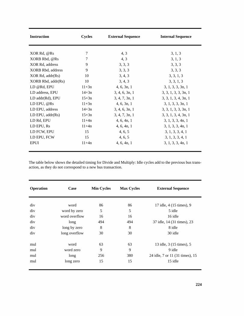
224
The table below shows the detailed timing for Divide and Multiply: Idle cycles add to the previous bus trans-action, as they do not correspond to a new bus transaction.
Instruction Cycles External Sequence Internal Sequence
XOR Rd, @Rs 7 4, 3 3, 1, 3
XORB Rbd, @Rs 7 4, 3 3, 1, 3XOR Rd, address 9 3, 3, 3 3, 3, 3
XORB Rbd, address 9 3, 3, 3 3, 3, 3
XOR Rd, addr(Rs) 10 3, 4, 3 3, 3, 1, 3XORB Rbd, addr(Rs) 10 3, 4, 3 3, 3, 1, 3
LD @Rd, EPU 11+3n 4, 6, 3n, 1 3, 1, 3, 3, 3n, 1
LD address, EPU 14+3n 3, 4, 6, 3n, 1 3, 3, 1, 3, 3, 3n, 1
LD addr(Rd), EPU 15+3n 3, 4, 7, 3n, 1 3, 3, 1, 3, 4, 3n, 1LD EPU, @Rs 11+3n 4, 6, 3n, 1 3, 1, 3, 3, 3n, 1
LD EPU, address 14+3n 3, 4, 6, 3n, 1 3, 3, 1, 3, 3, 3n, 1
LD EPU, addr(Rs) 15+3n 3, 4, 7, 3n, 1 3, 3, 1, 3, 4, 3n, 1LD Rd, EPU 11+4n 4, 6, 4n, 1 3, 1, 3, 3, 4n, 1
LD EPU, Rs 11+4n 4, 6, 4n, 1 3, 1, 3, 3, 4n, 1
LD FCW, EPU 15 4, 6, 5 3, 1, 3, 3, 4, 1LD EPU, FCW 15 4, 6, 5 3, 1, 3, 3, 4, 1
EPUI 11+4n 4, 6, 4n, 1 3, 1, 3, 3, 4n, 1
Operation Case Min Cycles Max Cycles External Sequence
div word 86 86 17 idle, 4 (15 times), 9
div word by zero 5 5 5 idlediv word overflow 16 16 16 idle
div long 494 494 37 idle, 14 (31 times), 23
div long by zero 8 8 8 idlediv long overflow 30 30 30 idle
mul word 63 63 13 idle, 3 (15 times), 5mul word zero 9 9 9 idle
mul long 256 380 24 idle, 7 or 11 (31 times), 15
mul long zero 15 15 15 idle

225
Appendix 2Unimplemented Features/Instructions
Revision 1 of the Y8002 design does not implement a number of features and instructions of the Z8000architecture. Unimplemented features include the refresh mechanism (although the REFRESH register isimplemented), System/User mode of operation (only System mode is supported and the SYS bit in the FCWis forced High), and the Extended Processing architecture (the EPA bit in the FCW is forced Low). Eventhough Normal mode is not supported, the Normal Stack Pointer is present.
Unimplemented instructions are listed in the table below:
Note that any of these instructions can be easily added to the design if required.
Instruction Opcode (first word only)
LD @Rd, EPU 00001111_Rdnz_11xx
LD address, EPU 01001111_0000_11xx
LD addr(Rd), EPU 01001111_Rdnz_11xxLD EPU, @Rs 00001111_Rsnz_01xx
LD EPU, address 01001111_0000_01xx
LD EPU, addr(Rs) 01001111_Rsnz_01xxLD Rd, EPU 10001111_0xxx_00xx
LD EPU, Rs 10001111_0xxx_10xx
LD FCW, EPU 10001110_xxxx_00xxLD EPU, FCW 10001110_xxxx_10xx
EPUI 10001110_xxxx_01xx

226

229
Appendix 3 Trapped Opcodes
This Appendix lists all of the instruction ecodings which will result in an Unimplemented Instruction trap,along with the valid instructions included with each encoding.
Opcode Instruction(s)
0x00110x_xxxx_xx11 Reserved
0x00110x_xxxx_1x1x Reserved
0x00110x_xxxx_11xx Reserved0x001100_xxxx_1xx1 Reserved
01001101_xxxx_1xx1 Reserved
x0001100_xxxx_xx11 Reservedx0001100_xxxx_1x1x Reserved
x0001100_xxxx_11xx Reserved
10001101_xxxx_1xx1 Reserved10001101_xxxx_1x1x Reserved
10001101_xxxx_11xx Reserved
0x011100_xxxx_0000 Reserved0x011100_xxxx_xx1x Reserved
0x011100_xxxx_x1xx Reserved
0x00111x_xxxx_xxxx EPUx000111x_xxxx_xxxx EPU
00110110_xxxx_xxxx Reserved
00111000_xxxx_xxxx Reserved00111001_xxxx_xxx1 Reserved
00111001_xxxx_xx1x Reserved
00111001_xxxx_x1xx Reserved00111001_xxxx_1xxx Reserved
0011101x_xxxx_11xx Reserved
01111011_xxxx_0xx1 Reserved01111011_xxxx_0x10 Reserved
01111011_xxxx_x011 Reserved
01111011_xxxx_x100 Reserved01111011_xxxx_111x Reserved

230
Opcode Instruction(s)
01111000_xxxx_xxxx Reserved
01111001_xxxx_xxx1 Reserved01111001_xxxx_xx1x Reserved
01111001_xxxx_x1xx Reserved
01111001_xxxx_1xxx Reserved01111101_xxxx_x00x Reserved
01111101_xxxx_x1x0 Reserved
0111111x_xxxx_xxxx Reserved, SC
1001110x_xxxx_xxx1 Reserved1001110x_xxxx_xx1x Reserved
1001110x_xxxx_x1xx Reserved
1001110x_xxxx_0xxx Reserved100111x1_xxxx_xxxx Reserved
10110010_xxxx_x1x1 Reserved
10111001_xxxx_xxxx Reserved10111000_xxxx_xxx1 Reserved
1011101x_xxxx_x011 Reserved
1011101x_xxxx_x1x1 Reserved10111111_xxxx_xxxx Reserved

231
Appendix 4 Known Timing Differences
Every effort has been made to match the documented operation of the original Z8002 microprocessor as faras timing is concerned. However, there are three cases where this was not possible, and these are describedin this Appendix. The cases are Interrupt Acknowledge timing, the Divide instruction, and the Multiplyinstruction.
In addition to the known timing differences, there are a number of cases of potential timing differences.These cases arise where the Zilog documentation is either incomplete or undefined. The cases that are poten-tially different are Shift and Shift Dynamic with zero shift, Shift and Shift Dynamic with an out-of-rangeshift value, and Halt when responding to an interrupt. If the Z8002 behavior is logical, the Y8002 designprobably matches it.
The interrupt acknowledge cycle timing includes an aborted IF1 bus transaction. In the Y8002 design thistransaction is always four clock cycles in length (plus any Wait states). The Zilog documentation states thatthis bus transaction may be anywhere from three to seven clock cycles long (plus Wait states) but does notindicate why this is the case. Variable timing for this instance does not seem logical and the Y8002 designdoes not attempt to match this behavior.
The Divide instruction differences are shown in the table below. Note that the numbers in the Zilog docu-mentation are somewhat suspicious because they do not appear to correctly account for the differentaddressing modes.
Divide Y8002 timing published Z8002 timingInstruction normal div-by-0 overflow normal div-by-0 overflow
DIV RRd, Rs 92 11 22 107 13 25DIV RRd, #data 94 13 24 107 13 25DIV RRd, @Rs 94 13 24 107 13 25DIV RRd, address 96 15 26 108 14 26DIV RRd, addr(Rs) 97 16 27 109 15 27
DIVL RQd, RRs 500 14 36 744 30 51DIVL RQd, #data 505 19 41 744 30 51DIVL RQd, @Rs 505 19 41 744 30 51DIVL RQd, address 507 21 43 745 31 52DIVL RQd, addr(Rs) 508 22 44 746 32 53

232
The Multiply instruction differences are shown in the table below. As in the case of Divide, the Zilog docu-mentation does not appear to correctly account for the different addressing modes. In addition, the sevenclock cycle difference, depending on whether an operand bit is one or zero in the case of MULTL, seemsexcessive.
Multiply Y8002 timing published Z8002 timingInstruction min max zero result min max zero result
MULT RRd, Rs 69 69 15 70 70 18MULT RRd, #data 71 71 17 70 70 18MULT RRd, @Rs 71 71 17 70 70 18MULT RRd, address 73 73 19 71 71 19MULT RRd, addr(Rs) 74 74 20 72 72 20
MULTL RQd, RRs 262 386 21 289 506 30MULTL RQd, #data 267 391 26 289 506 30MULTL RQd, @Rs 267 391 26 289 506 30MULTL RQd, address 269 393 28 290 507 31MULTL RQd, addr(Rs) 270 394 29 291 508 32