y. sun and j.a. rogers, “inorganic semiconductors for flexible
TRANSCRIPT

DOI: 10.1002/adma.200602223
Inorganic Semiconductors for FlexibleElectronics**
By Yugang Sun* and John A. Rogers*
1. Introduction
Electronic systems that can cover large areas on flexiblesubstrates have received increasing attention in the last cou-ple of decades because they enable classes of applications thatlie outside those easily addressed with wafer-based electron-
ics. Examples include flexible displays, electronic textiles, sen-sory skins, and active antennas.[1,2] This type of electronics,sometimes referred to as macroelectronics, differs from estab-lished microelectronic and nanoelectronic systems, whereprogress is driven primarily by reducing the critical dimen-sions of the functional elements (e.g., channel lengths and di-electric thicknesses in transistors) to increase the speed andcomputing capacity and to reduce the operating voltages.Macroelectronics, instead, uses thin-film transistors (TFTs)distributed over large areas where, in existing applicationsthat use glass substrates, they provide switching elements inactive-matrix liquid-crystal displays (AMLCDs) or medicalX-ray imaging devices.[3] Here, the overall size of the systemsrather than the minimum feature size of an individual circuitcomponent represents the primary scaling metric. Amorphoussilicon (a-Si) is currently the dominant semiconductor usedfor transistors in these systems. In fact, this material is nowthe second most economically significant semiconductor, be-hind single-crystal silicon. An emerging direction in researchis to develop alternative materials and patterning techniquesfor these macroelectronic systems, with a goal of increasingtheir performance, decreasing their cost (per unit area), andenabling them to be formed on low-cost, bendable substrates.Low-temperature deposition or printing-type techniques forfabricating of high-quality semiconductor films on substratessuch as metal foils,[4] plastic sheets,[5] and even paper[6] are of
REV
IEW
Adv. Mater. 2007, 19, 1897–1916 © 2007 WILEY-VCH Verlag GmbH & Co. KGaA, Weinheim 1897
–[*] Dr. Y. Sun
Center for Nanoscale MaterialsArgonne National Laboratory9700 South Cass Avenue, Argonne, IL 60439 (USA)E-mail: [email protected]. J. A. RogersDepartment of Materials Science and EngineeringBeckman Institute and Frederick Seitz Materials ResearchLaboratoryUniversity of Illinois at Urbana-ChampaignUrbana, IL 61801 (USA)E-mail: [email protected]
[**] The work was supported by the U.S. Department of Energy underGrant No. DEFG02-91-ER45439 and also partially supported by theDefense Advanced Projects Agency under Contract No. F8650-04-C-710. Devices were fabricated using the Microfabrication and CrystalGrowth Facility in Frederick Seitz Materials Research Laboratory,University of Illinois, which is partially supported by the U.S. De-partment of Energy under Grant No. DEFG02-91-ER45439. ArgonneNational Laboratory’s work was supported by the U.S. Departmentof Energy, Office of Science, Office of Basic Energy Sciences, undercontract DE-AC02-06CH11357.
This article reviews several classes of inorganic semiconductor materi-als that can be used to form high-performance thin-film transistors(TFTs) for large area, flexible electronics. Examples ranging from thinfilms of various forms of silicon to nanoparticles and nanowires ofcompound semiconductors are presented, with an emphasis on meth-ods of depositing and integrating thin films of these materials into devices. Performance charac-teristics, including both electrical and mechanical behavior, for isolated transistors as well as cir-cuits with various levels of complexity are reviewed. Collectively, the results suggest that flexibleor printable inorganic materials may be attractive for a range of applications not only in flexiblebut also in large-area electronics, from existing devices such as flat-panel displays to more chal-lenging (in terms of both cost and performance requirements) systems such as large area radio-frequency communication devices, structural health monitors, and conformal X-ray imagers.
particular interest. Integrating semiconductors with plasticsubstrates, which are the most attractive type of flexible sub-strate for many applications, requires processing temperaturesbelow the glass-transition or thermal-degradation tempera-tures of the plastics. Although many promising results havebeen obtained with thin films of small-molecule organics andpolymers,[7] the electrical performance that can be obtainedfrom them is still too low (comparable to a-Si in the bestcases) for many potential applications. Even with high-puritysingle crystals of these materials the mobilities are less thanthose of polycrystalline silicon.[8,9] Furthermore, the uncertainlong-term reliability and lack of controlled doping techniquesfor these materials represent other areas that require furtherresearch.
By contrast, many inorganic semiconductors exhibit highcarrier mobilities and excellent stability.[10] The main chal-lenge, for uses in macroelectronics on plastics, for example, isthat forming high-quality films of these materials and certainsteps associated with processing them into devices requiretemperatures that exceed the glass-transition and/or thermal-decomposition temperatures of the plastics. Also, many as-pects of the growth and processing do not scale easily to largeareas without the use of complex manufacturing systems.Progress in the last several years, however, has led to exam-ples of methods that avoid these limitations. This Reviewsummarizes some of this work, with an emphasis on inorganicsemiconductor films that have been, or have the potential to
be, integrated with plastic substrates to generate high-perfor-mance TFTs. The materials include films of silicon with var-ious levels of crystallinity (i.e., from amorphous to poly- andmonocrystalline), transparent oxides, chalcogenides, nano-wires synthesized via “bottom-up” chemical routes, andnano-/microstructures fabricated from wafers via “top-down”approaches. This article reviews the properties achievablewith these materials, using field-effect mobilities (as deter-mined by standard analysis of characteristics measured intransistor devices) and on/off current ratios as the primarymetrics. The content is organized according to the materialtype, with discussions of the techniques for growing the filmsand illustrative examples of devices and circuits that havebeen built with them. The last section presents some perspec-tives on the trends for future work.
2. Films of Silicon—From Amorphousto Large-Grained Polycrystalline
TFTs fabricated with hydrogen-terminated amorphous Si(a-Si:H) represent, by far, the most successful systems for ap-plications in large-area electronics. Silicon films with variousdegrees of crystallinity and mobilities that can be orders ofmagnitude larger than a-Si:H can be formed using a-Si precur-sor films and thermal treatments. These films are classified asnanocrystalline Si (nc-Si), microcrystalline Si (lc-Si), and
REV
IEW
Y. Sun and J. A. Rogers/Inorganic Semiconductors for Flexible Electronics
1898 www.advmat.de © 2007 WILEY-VCH Verlag GmbH & Co. KGaA, Weinheim Adv. Mater. 2007, 19, 1897–1916
John A. Rogers, obtained B.A. and B.Sc. degrees in chemistry and in physics from the Universityof Texas, Austin, in 1989. From MIT, he received S.M. degrees in physics and in chemistry in1992 and a Ph.D. degree in physical chemistry in 1995. From 1995 to 1997, he was a Junior Fel-low in the Harvard University Society of Fellows. During this time he also served as a Directorfor Active Impulse Systems, a company based on his Ph.D. research that he co-founded in 1995and that was acquired by a large company in 1998. He joined Bell Laboratories as a Member ofTechnical Staff in the Condensed Matter Physics Research Department in 1997, and served asDirector of this department from 2000–2002. He is currently Founder Professor of Engineeringat University of Illinois at Urbana/Champaign, with appointments in the Departments of Materi-als Science and Engineering, Electrical and Computer Engineering, Mechanical Science and En-gineering and Chemistry. His research includes fundamental and applied aspects of nano- andmolecular-scale fabrication, materials and patterning techniques for large-area electronics andunusual photonic systems. He has won many awards for this work, which is published in morethan 150 papers and ca. 60 patents, more than half of which are licensed or in active use.
Yugang Sun received B.Sc. and Ph.D. degrees in chemistry from the University of Science andTechnology of China (USTC) in 1996 and 2001, respectively. From 2001 to 2006, he was a re-search associate at the University of Washington and University of Illinois at Urbana-Cham-paign, where he invented a number of technologies for fabricating nanostructures with controlledshapes and flexible transistors with operation speeds in the gigahertz regime. He is currently anassistant scientist for the Center for Nanoscale Materials in Argonne National Laboratory. Hisresearch interests include synthesis and characterization of nanostructures, micro-/nanofabrica-tion, nanobiotechnology, and devices for optics and electronics. He has published more than 60papers and book chapters.
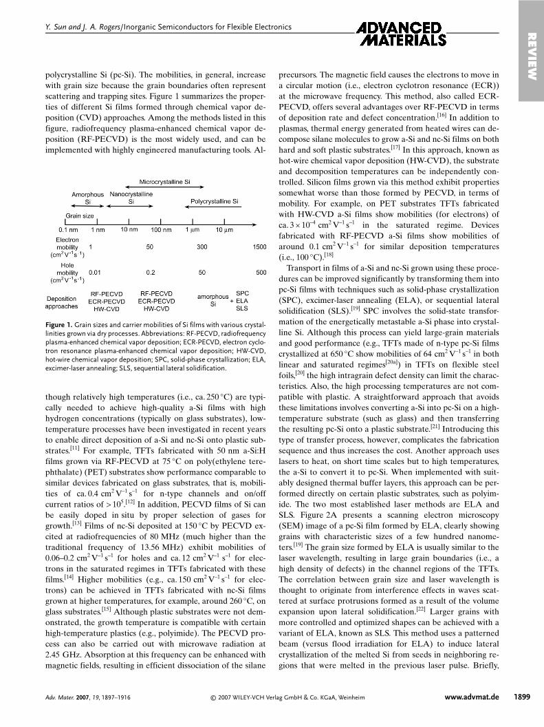
polycrystalline Si (pc-Si). The mobilities, in general, increasewith grain size because the grain boundaries often representscattering and trapping sites. Figure 1 summarizes the proper-ties of different Si films formed through chemical vapor de-position (CVD) approaches. Among the methods listed in thisfigure, radiofrequency plasma-enhanced chemical vapor de-position (RF-PECVD) is the most widely used, and can beimplemented with highly engineered manufacturing tools. Al-
though relatively high temperatures (i.e., ca. 250 °C) are typi-cally needed to achieve high-quality a-Si films with highhydrogen concentrations (typically on glass substrates), low-temperature processes have been investigated in recent yearsto enable direct deposition of a-Si and nc-Si onto plastic sub-strates.[11] For example, TFTs fabricated with 50 nm a-Si:Hfilms grown via RF-PECVD at 75 °C on poly(ethylene tere-phthalate) (PET) substrates show performance comparable tosimilar devices fabricated on glass substrates, that is, mobili-ties of ca. 0.4 cm2 V–1 s–1 for n-type channels and on/offcurrent ratios of > 105.[12] In addition, PECVD films of Si canbe easily doped in situ by proper selection of gases forgrowth.[13] Films of nc-Si deposited at 150 °C by PECVD ex-cited at radiofrequencies of 80 MHz (much higher than thetraditional frequency of 13.56 MHz) exhibit mobilities of0.06–0.2 cm2 V–1 s–1 for holes and ca. 12 cm2 V–1 s–1 for elec-trons in the saturated regimes in TFTs fabricated with thesefilms.[14] Higher mobilities (e.g., ca. 150 cm2 V–1 s–1 for elec-trons) can be achieved in TFTs fabricated with nc-Si filmsgrown at higher temperatures, for example, around 260 °C, onglass substrates.[15] Although plastic substrates were not dem-onstrated, the growth temperature is compatible with certainhigh-temperature plastics (e.g., polyimide). The PECVD pro-cess can also be carried out with microwave radiation at2.45 GHz. Absorption at this frequency can be enhanced withmagnetic fields, resulting in efficient dissociation of the silane
precursors. The magnetic field causes the electrons to move ina circular motion (i.e., electron cyclotron resonance (ECR))at the microwave frequency. This method, also called ECR-PECVD, offers several advantages over RF-PECVD in termsof deposition rate and defect concentration.[16] In addition toplasmas, thermal energy generated from heated wires can de-compose silane molecules to grow a-Si and nc-Si films on bothhard and soft plastic substrates.[17] In this approach, known ashot-wire chemical vapor deposition (HW-CVD), the substrateand decomposition temperatures can be independently con-trolled. Silicon films grown via this method exhibit propertiessomewhat worse than those formed by PECVD, in terms ofmobility. For example, on PET substrates TFTs fabricatedwith HW-CVD a-Si films show mobilities (for electrons) ofca. 3 × 10⁻⁴ cm2 V–1 s–1 in the saturated regime. Devicesfabricated with RF-PECVD a-Si films show mobilities ofaround 0.1 cm2 V–1 s–1 for similar deposition temperatures(i.e., 100 °C).[18]
Transport in films of a-Si and nc-Si grown using these proce-dures can be improved significantly by transforming them intopc-Si films with techniques such as solid-phase crystallization(SPC), excimer-laser annealing (ELA), or sequential lateralsolidification (SLS).[19] SPC involves the solid-state transfor-mation of the energetically metastable a-Si phase into crystal-line Si. Although this process can yield large-grain materialsand good performance (e.g., TFTs made of n-type pc-Si filmscrystallized at 650 °C show mobilities of 64 cm2 V–1 s–1 in bothlinear and saturated regimes[20a]) in TFTs on flexible steelfoils,[20] the high intragrain defect density can limit the charac-teristics. Also, the high processing temperatures are not com-patible with plastic. A straightforward approach that avoidsthese limitations involves converting a-Si into pc-Si on a high-temperature substrate (such as glass) and then transferringthe resulting pc-Si onto a plastic substrate.[21] Introducing thistype of transfer process, however, complicates the fabricationsequence and thus increases the cost. Another approach useslasers to heat, on short time scales but to high temperatures,the a-Si to convert it to pc-Si. When implemented with suit-ably designed thermal buffer layers, this approach can be per-formed directly on certain plastic substrates, such as polyim-ide. The two most established laser methods are ELA andSLS. Figure 2A presents a scanning electron microscopy(SEM) image of a pc-Si film formed by ELA, clearly showinggrains with characteristic sizes of a few hundred nanome-ters.[19] The grain size formed by ELA is usually similar to thelaser wavelength, resulting in large grain boundaries (i.e., ahigh density of defects) in the channel regions of the TFTs.The correlation between grain size and laser wavelength isthought to originate from interference effects in waves scat-tered at surface protrusions formed as a result of the volumeexpansion upon lateral solidification.[22] Larger grains withmore controlled and optimized shapes can be achieved with avariant of ELA, known as SLS. This method uses a patternedbeam (versus flood irradiation for ELA) to induce lateralcrystallization of the melted Si from seeds in neighboring re-gions that were melted in the previous laser pulse. Briefly,
REV
IEWY. Sun and J. A. Rogers/Inorganic Semiconductors for Flexible Electronics
Adv. Mater. 2007, 19, 1897–1916 © 2007 WILEY-VCH Verlag GmbH & Co. KGaA, Weinheim www.advmat.de 1899
Figure 1. Grain sizes and carrier mobilities of Si films with various crystal-linities grown via dry processes. Abbreviations: RF-PECVD, radiofrequencyplasma-enhanced chemical vapor deposition; ECR-PECVD, electron cyclo-tron resonance plasma-enhanced chemical vapor deposition; HW-CVD,hot-wire chemical vapor deposition; SPC, solid-phase crystallization; ELA,excimer-laser annealing; SLS, sequential lateral solidification.

SLS uses an iterative process that involves two (or more)well-defined steps: i) laser irradiation that completely meltsthe Si in a localized region, resulting in lateral growth ofgrains that initiate from the periphery of the melted spot; andii) additional irradiation using spatially translated pulses thatmelt the Si next to the originally irradiated spot such that theexisting grains grow epitaxially to extend the size of the crys-talline regions. As a result, SLS always produces grains withmuch larger sizes, better-controlled shapes, and higher de-grees of uniformity compared to ELA.[23] Figure 2B shows anSEM image of a Si film converted through line-scan SLS, indi-cating the formation of stripes of crystalline Si with high as-pect ratios (i.e., the ratio of length to width),[19] which, whenoriented along the channel in a transistor, can offer high mo-
bility transport. In addition, other microstructures of crystal-line Si can be obtained via various SLS schemes, as controlledby the patterns of the laser beams and the sequences of thepulses.[24] With thermal buffer layers, SLS can generate pc-Sifilms with quality similar to that shown in Figure 2B on plasticsubstrates (e.g., polyimide sheets with thicknesses of 10 lmformed on Si wafers).[25] Figure 2C shows the transfer charac-teristics of a transistor with a channel length of 10 lm andchannel width of 100 lm, fabricated with n-type pc-Si film onpolyimide. The mobility (for electrons) and threshold voltage(Vth) for this device are 191 cm2 V–1 s–1 and 1.1 V, respectively.Microwave measurements indicate unity current gain fre-quencies (fT) as high as 257 MHz for transistors with channellengths of 2 lm (Fig. 2D). Because a-Si films can be easily
REV
IEW
Y. Sun and J. A. Rogers/Inorganic Semiconductors for Flexible Electronics
1900 www.advmat.de © 2007 WILEY-VCH Verlag GmbH & Co. KGaA, Weinheim Adv. Mater. 2007, 19, 1897–1916
Figure 2. A,B) SEM images of defect-etched pc-Si films obtained by processing PECVD a-Si layers with different pulsed-laser crystallization techniques:A) ELA; B) line-scan SLS. These images show the different crystalline structures in the pc-Si films. Reproduced with permission from [19]. Copyright2006 Materials Research Society. C–E) Characterization of TFTs and circuits fabricated with pc-Si films on polyimide substrates obtained by SLS.C) Transfer characteristics of an n-type TFT with channel length and width of 10 and 100 lm, respectively, measured at VDS = 1 V. D) Microwave evalua-tion of an n-type TFT (channel length 2 lm). The unity current gain frequency (fT) is the frequency at which the current gain passes through unity(0 dB gain). E) Output waveform of a five-stage, complementary metal-oxide semiconductor (CMOS) ring oscillator, fabricated with n- and p-type pc-Sifilms on a polyimide substrate and evaluated at drive bias (VDD) of 15 V. The TFTs have channel lengths of 2 lm. The frequency is approximately100 MHz. Adapted with permission from [25]. Copyright 2005 IEEE. F) Transmission electron microscopy (TEM) image of a pc-Si film formed usingan a-Si layer deposited from a liquid precursor. The inset shows a high-resolution TEM image. G,H) Electrical characteristics of TFTs fabricated withpc-Si films shown in (F). The properties of different pc-Si films obtained through various approaches are also compared in (G). Adapted with permis-sion from [27]. Copyright 2006 Nature Publishing Group.

doped in situ during deposition by controlling the feed gases,p-type metal-oxide semiconductor (PMOS) field-effect tran-sistors made of pc-Si films can also be fabricated. Such deviceson polyimide sheets also display good performance: mobility(for holes) of 45 cm2 V–1 s–1, Vth of –13.9 V, and fT of 184 MHzfor devices with channel lengths of 2 lm. Integrating n- andp-type devices generates flexible complementary metal-oxidesemiconductor (CMOS) inverters and more complex circuits.Figure 2E shows output waveforms from a five-stage CMOSring oscillator (with device channel lengths of 2 lm) with anoscillation frequency of ca. 100 MHz. Similar procedures canalso be carried out on bendable steel foils to yield pc-Si TFTswith comparable performance.[26] Steel foils are attractive inthis case because they do not require the thick thermalbuffer stacks that are needed with plastic. They have the dis-advantages that, compared with certain plastics, they are rela-tively expensive; they are not lightweight; they require spe-cialized processing and conformal coatings to generatesmooth surfaces; they are opaque, which, for example, pre-vents their use in backlit displays; and they are conductive,which leads to parasitic capacitance that can limit high-speedperformance.
Although CVD techniques currently provide the most ef-fective and versatile approaches to depositing Si, solution-printing techniques could be valuable as low-cost alternatives.Recent work shows, for example, that solutions of polysilanesformed by photopolymerization of cyclopentasilane (CPS)dissolved in a mixed solvent of CPS and toluene, referred toas liquid Si, can generate a-Si as well as pc-Si films.[27] The fab-rication in this case begins with spin-casting a film of this liq-uid Si. Prebaking drives the volatile solvent components (CPSand toluene) out of the film. The Si–Si bonds in the polysilanestart to break at temperatures near 280 °C, and a fraction ofthe polysilane is released as SiH2 and SiH3. At higher temper-atures (i.e., ca. 300 °C) the Si–H bonds break and Si atomsstart to polymerize, resulting in the formation of a 3D a-Sinetwork. Bottom-gate TFTs fabricated with a-Si films gener-ated in this manner and further baked at 540 °C for 2 h exhibitmobilities (for electrons) of only 10–3–10–4 cm2 V–1 s–1, whichis three or four orders of magnitude smaller than that of a-Siobtained through PECVD. The poor mobility can be attribut-ed to the low concentration of hydrogen (0.3 %) in a-Si filmsformed at 540 °C, which leads to appreciable quantities ofdangling bonds that frustrate transport. Although spin-coatedfilms baked at 300 °C or lower contain more than 20 % hydro-gen, they are not completely transformed into a-Si and can beeasily oxidized in air. The a-Si films can, however, be laser-an-nealed (308 nm XeCl excimer) to convert them into pc-Si.The transmission electron microscopy (TEM) image in Fig-ure 2F shows the polycrystalline nature of films produced inthis manner. Figure 2G compares the transfer curves of TFTs(with the same geometry) built with pc-Si films formed bylaser annealing of a solution-cast film of a-Si and one formedby conventional CVD. The mobilities (for electrons) of de-vices that use the solution-deposited a-Si are as high as108 cm2 V–1 s–1, slightly lower than those that used CVD a-Si.
Figure 2H plots the current–voltage (IDS–VDS) curves of atypical TFT at different gate voltages (VGS). Solution process-ing is interesting because it allows films of a-Si to be printed,for example, through ink-jet nozzles. The thickness variationsassociated with such printed films, however, lead to poorproperties in the laser annealed films (Fig. 2G). Obtaininguniform films, and optimizing the physical properties of theliquid precursor, such as its stability in an ambient environ-ment, its viscosity, vapor pressure, and surface tension, repre-sent areas for future work. In addition, the relatively hightemperatures (e.g., 540 °C) needed to form the a-Si may pre-vent this method, in its current form, from being used withplastic substrates.
3. Films of Transparent Oxides
Oxides of transition metals, such as ZnO and its derivatives,provide another class of inorganic semiconductor for large-area electronics. These oxides are usually transparent in thevisible owing to their large bandgaps of > 3 eV. This opticalproperty, when combined with transparent conductors and di-electrics, allows unusual applications, such as invisible elec-tronics for heads-up displays on windshields or cockpit enclo-sures. Such oxide thin films, with properties suitable for TFTs,can be formed on both inorganic and plastic substrates byeither gas-phase deposition or solution processes. The mobili-ties that can be achieved using the processes described in thefollowing sections are in the range of ca. 1–70 cm2 V–1 s–1 withtypical values of approximately 10 cm2 V–1 s–1.
3.1. ZnO Films Deposited From the Gas Phase
Radiofrequency magnetron sputtering[28] and pulsed-laserdeposition[29] are the most commonly used techniques to formfilms of ZnO for device applications. In a typical process,ZnO removed from a solid target by use of these methods de-posits on the surface of a substrate, usually at or near roomtemperature, in a vacuum chamber. An appropriate pressureof O2 helps to eliminate defects (i.e., oxygen vacancies). Simi-lar deposition techniques can also grow doped ZnO films withhigh conductivities, suitable for use as electrodes, by using tar-gets that consist of mixtures of ZnO and dopants (e.g., Al2O3
and Ga2O3).[28] ZnO films formed in this way crystallize intograins with sizes in the range of several nanometers to tens ofnanometers, resulting in surface roughness of several nanome-ters (see the typical SEM image shown in Fig. 3A).[30] Thisroughness can be important, depending on the device layout,because it can frustrate the use of (nonconformal) thin-filmdielectrics (< 10 nm) and it can degrade transport characteris-tics.[31] Increasing the substrate temperatures and/or post-ther-mal-annealing treatments can increase the grain size, which,in turn, can enhance device performance.
Figure 3B shows the geometry of some transparent TFTsfabricated with a ZnO film deposited at room temperature.[32]
REV
IEWY. Sun and J. A. Rogers/Inorganic Semiconductors for Flexible Electronics
Adv. Mater. 2007, 19, 1897–1916 © 2007 WILEY-VCH Verlag GmbH & Co. KGaA, Weinheim www.advmat.de 1901

In this case, a glass slide coated with anindium tin oxide (ITO) layer (100 nmthick) as a gate electrode provides asubstrate on which a film of silicon oxy-nitride (SiOxNy; 200 nm thick) as thegate dielectric and a semiconductingfilm of ZnO (150 nm thick) are sequen-tially deposited via radiofrequency mag-netron sputtering at room temperature.Films of Ga-doped ZnO (GZO; 100 nmthick) patterned by a lift-off process de-fine the source and drain electrodes.These processes yield transparent TFTswith channel lengths and widths of 40and 200 lm, respectively. The transpar-ency of the materials (including theglass substrate of 1.1 mm thickness), aswell as the TFTs in a spectral range of300–1500 nm, are shown in Figure 3C.The average transmittance in the visibleregion is as high as 84 % for the TFTs.The comparison in Figure 3C indicatesthat transmission losses due to the ZnOTFTs (vs. the pristine glass substratewith ITO layer) are negligible(ca. 4 %). The inset shows a glass sub-strate (5 × 5 cm2) covered by arrays ofZnO TFTs, through which an underly-ing logo is clearly visible. Electricalmeasurements indicate enhancement-mode n-type operation of these devices.Figure 3D presents a transfer curvefrom a typical transistor in the satura-tion regime (i.e., VDS = 10 V). The mo-bility (for electrons) and Vth of this de-vice are ca. 70 cm2 V–1 s–1 and 1.8 V,respectively. The on/off current ratio is5 × 105. Results of initial studies indicatethat these devices are stable in an ambi-ent environment.[33] In addition, p-typeZnO can be grown by doping theintrinsic n-type ZnO films with phos-phorus (e.g., P2O5)[34] or arsenic (e.g.,Zn3As2).[35] The availability of both n-and p-type ZnO enables the possibilityof transparent CMOS circuits. Althoughall the reported devices are on rigid sub-strates, for example, glass and Si wafers,devices on plastic substrates might bepossible because the materials can bedeposited at low temperatures. Usingpulsed-laser deposition, polycrystallineZnO films (with grain size of 17 nm)have been successfully deposited on aflexible polyimide sheet, but no deviceresults were reported.[36]
REV
IEW
Y. Sun and J. A. Rogers/Inorganic Semiconductors for Flexible Electronics
1902 www.advmat.de © 2007 WILEY-VCH Verlag GmbH & Co. KGaA, Weinheim Adv. Mater. 2007, 19, 1897–1916
Figure 3. A) SEM image of a ZnO film deposited by radio frequency magnetron sputtering, show-ing the polycrystalline characteristics of the film. Reproduced with permission from [30]. Copyright2005 Elsevier B.V. B) Geometry, C) optical, and D) electrical characterization of transparent TFTsfabricated with ZnO films as the semiconductor. Adapted with permission from [32]. Copyright2004 Elsevier B.V. E,F) Atomic force microscopy images of assembled films formed by spin-castingdispersions of ZnO nanospheres and ZnO nanorods, respectively. G,H) Electrical characteristics ofTFTs fabricated with films shown in (E,F). (G) and (H) correspond to the films of ZnO nanospheresand nanorods, respectively. Reproduced with permission from [39]. Copyright 2005 AmericanChemical Society.

3.2. ZnO Films Spin-Cast From Colloidal Solutions
ZnO films can also be formed by spin-coating solution sus-pensions of ZnO nanocrystals in the form of chemicallysynthesized and functionalized spheres or rods. Control overreaction conditions and recipes allows the dimensions, shapes,and compositions of ZnO colloids to be selected over a widerange.[37,38] High-concentration (> 50 mg mL–1) suspensions ofcolloidal ZnO are generally desired, and can be achieved byattaching long-chain surfactant molecules to the ZnO sur-faces. For example, ZnO nanoparticles with diameters ofca. 6 nm and nanorods with widths and lengths of 10 and65 nm, respectively, and chemically modified with butylamine(with a low boiling point of 78 °C) can be dispersed in chloro-form at concentrations of ca. 90 mg mL–1. Spin-casting themonto SiO2(300 nm)/Si wafers with prepatterned interdigitatedCr(3 nm)/Au(12 nm) source and drain electrodes form ZnOTFTs where the SiO2 and Si provide the gate dielectric andthe gate, respectively.[39] Annealing these devices at 230 °C informing gas (N2/H2 of 95:5 v/v) for 30 min increases their sta-bility and performance. Figure 3E and F shows atomic forcemicroscopy (AFM) images of films of ZnO nanospheres andnanorods. These data reveal close-packed assemblies ofspheres and in-plane aligned arrays of rods. The alignmentand relatively large size of the nanorods, compared with thenanospheres, reduces the effective number of interfaces in thechannel. Figure 3G and H compares the electrical characteris-tics (i.e., transfer curves in both linear and saturated regimes)of TFTs formed with films of ZnO nanospheres and nanorods,respectively. In both cases, the devices exhibit n-type transis-tor behavior. The mobilities of nanosphere TFTs extractedfrom the plots (Fig. 3G) are 2 × 10⁻⁴ cm2 V–1 s–1 in the linearregime and 4 × 10⁻⁴ cm2 V–1 s–1 in the saturated regime, whilethe linear and saturated mobilities for nanorod TFTs are 0.01and 0.02 cm2 V–1 s–1, respectively (Fig. 3H). The performancecan be improved by further post-deposition processes, that is,hydrothermal growth in an aqueous solution of zinc nitrateand ethyldiamine at 90 °C. These procedures increase the mo-bilities of the nanorod TFTs to 0.2 and 0.6 cm2 V–1 s–1 in thelinear and saturated regimes, respectively. These characteris-tics are, of course, much worse than those obtained withsputtered films, but are nevertheless interesting owing to thecompatibility of solution-based techniques with low cost,large-area deposition.
3.3. Films of ZnO-Based Binary and Ternary Oxides
ZnO can crystallize with other materials, such as In2O3,Ga2O3, and SnO2, to form binary or ternary oxides that aretransparent and offer high mobility. An example is single-crystalline InGaO3(ZnO)5 (IGZO) films, which can be epi-taxially grown on (111) single-crystal yttria-stabilized zirconia(YSZ) substrates, with mobilities as high as ca. 80 cm2 V–1 s–1
reported for TFTs fabricated using them.[40] Although suchresults are not directly relevant to the scope of this Review,
recent reports indicate that amorphous IGZO films with goodproperties can be formed on plastic substrates at room tem-perature.[41,42] In these systems, as well as for other amorphousoxide semiconductors containing post-transition-metal cations(e.g., ZnO:InIII), degenerate band conduction and large mo-bility are possible. Such behavior is different to that of amor-phous covalent semiconductors, such as Si, in which carriertransport is controlled by hopping between localized tail-states and band conduction is not achievable. The conductionband minimum (CBM) in typical wide-bandgap oxide semi-conductors (e.g., ZnO) is mainly composed of unoccupiedmetal ns orbitals (n denotes the principal quantum number),which can directly overlap neighboring metal ns orbitals togenerate carrier-transport pathways. In addition, ns orbitalswith large principal quantum numbers (i.e., n > 4) lead togreatly dispersed CBM, which in turn leads to high electronmobility if the carrier relaxation times are not significantlydifferent between the constituent materials.[43] As a result,amorphous oxide semiconductors can exhibit Hall-effect mo-bilities similar to those of their corresponding crystallinephases, even when grown at low temperatures. Figure 4Asummarizes the Hall mobility (lHall) and carrier concentra-tion (Ne) for films of In2O3–Ga2O3–ZnO systems depositedby pulsed-laser deposition at room temperature.[41] The resultsclearly show that high mobility (> 10 cm2 V–1 s–1) can beachieved in amorphous oxide systems, i.e., In2O3–Ga2O3
(a-IGO), Ga2O3–ZnO (a-GZO), In2O3–ZnO (a-IZO), andIn2O3–Ga2O3-ZnO (a-IGZO).
Figure 4B shows the layout of TFTs fabricated witha-IGZO on a PET substrate. In this top-gate configuration,high-k Y2O3 (with dielectric constant of ca. 16; k = dielectricconstant) and ITO serve as the gate dielectric layers andelectrodes, respectively. Figure 4C shows a photograph of aPET sheet with an array of a-IGZO TFTs, laminated on a cy-lindrical surface (with a radius of 30 mm) for probing, illus-trating the transparency and mechanical bendability.[42] Thedevices also exhibit good electrical performance when oper-ated at room temperature. Figure 4D shows a series of I–Vcurves from a TFT with the geometry shown in Figure 4B, re-corded at various gate biases in air. The thicknesses of thelayers of a-IGZO, Y2O3, and ITO are 30, 170, and 40 nm,respectively.[41a] The channel length and width of the transis-tors are 50 and 200 lm, respectively. The data indicate en-hancement-mode, n-type behavior. Both the linear and satu-ration values of mobility are ca. 10 cm2 V–1 s–1. The transfercharacteristics (Fig. 4E) show on/off current ratios of ca. 106.In this case, the off current is dominated by gate leakage(IGS), associated with the moderate quality of the low-tem-perature Y2O3 layer. The Vth and subthreshold slope(S = dVGS/dlogIDS) are +1.3 V and ca. 240 mV/decade, re-spectively, at VDS = 2 V. Devices on PET substrates continueto operate when bent to radii of curvature radius as small as30 mm (Fig. 4C), with only slight (10–15 %) reductions inmobility.
Transparent TFTs of this type are promising for a range ofapplications, such as backplanes for backlit liquid-crystal dis-
REV
IEWY. Sun and J. A. Rogers/Inorganic Semiconductors for Flexible Electronics
Adv. Mater. 2007, 19, 1897–1916 © 2007 WILEY-VCH Verlag GmbH & Co. KGaA, Weinheim www.advmat.de 1903

plays and for certain types of organic light-emitting diodes(OLEDs). This latter possibility has been demonstrated with
TFTs consisting of zinc tin oxide (ZTO;60 nm thick) as the semiconductor, ITO(Rsheet = 8 X/square) as the gate elec-trode, Al2O3/TiO2 (ATO; 220 nm thick)as the gate dielectric, and Al-dopedZnO (AZO; Rsheet = 8 X/square) as thesource and drain electrodes.[44] The de-vices show mobilities (for electrons) of11 cm2 V–1 s–1 in the saturated regime,on/off current ratios of 105, and trans-mittance > 80 % in the visible range.The OLEDs consist of sequentially de-posited electron-injection-enhancementlayers, bilayers of hole- and electron-transport hosts, hole-transport layers,hole-injection layers, and ITO anodelayers, integrated directly with the TFTs(further fabrication details are given byGörrn et al.[44]). Figure 4F shows anequivalent circuit of this hybrid inor-ganic–organic system and a set of lumi-nance–operation voltage (Vop) curves atdifferent gate voltages, indicating goodmodulation of the OLED emission.Figure 4G presents a photograph of asubstrate consisting of ten transparentactive-pixel devices, which sit on a back-ground of a seal logo. These kinds ofcapabilities can be important for manyapplications, although the processingapproaches, in their current form in-volve temperatures (ca. 350 °C) that aretoo high for most plastic substrates.Most recently, thin films of In2O3 com-bined with self-assembled thin organicdielectric layers have been used tofabricate transparent transistors withhigh performance: mobilities of> 120 cm2 V–1 s–1 and a low operationvoltage of ca. 1.0 V.[45]
4. Films of Chalcogenides
Chalcogenide compounds, includingsulfides, selenides, and tellurides, areclasses of semiconductors that havebeen used for transistors and other de-vices since the early days of solid-stateelectronics. In fact, the first TFT, dem-onstrated by Weimer in 1962, was fabri-cated with a thin film of polycrystallineCdS in a structure similar to that of met-al-semiconductor field-effect-transistors
(MESFETs).[46] Furthermore, the first AMLCD reported byBrody et al. in 1973 used CdSe-based TFTs as the pixel
REV
IEW
Y. Sun and J. A. Rogers/Inorganic Semiconductors for Flexible Electronics
1904 www.advmat.de © 2007 WILEY-VCH Verlag GmbH & Co. KGaA, Weinheim Adv. Mater. 2007, 19, 1897–1916
Figure 4. A) Room-temperature Hall mobility and carrier concentration as function of chemicalcompositions of the a-IGZO system. Values outside and inside parentheses show Hall mobilityand carrier concentration in units of cm2 V–1 s–1 and 1018 cm–3, respectively. B) Geometry of trans-parent TFTs fabricated with a-IGZO films on plastic PET sheets. C) Photograph of a flexible trans-parent TFT sheet bent to a radius of 30 mm. The TFT sheet is fully transparent in the visible spec-tral regime. D,E) Electrical characteristics of typical transparent TFTs using a-IGZO on flexibleplastic substrates Panels (A), (D), and (E) reproduced with permission from [41a]. Copyright 2006The Japan Society of Applied Physics. Panels (B) and (C) adapted with permission from [41b].Copyright: 2004 Nature Publishing Group. F,G) Characterization of active-pixels composed oftransparent TFTs using a-ZTO and OLEDs: dependence of luminance on the operating voltage(Vop) at different gate voltages (VGS) applied to the switching transistor (F), and photograph of anactive pixel in the “on” state (i.e., VGS = 4 V) (G). Adapted with permission from [44].

switches.[47a] Chalcogenide TFTs were successfully fabricatedin the 1970s on not only rigid glass slides but also flexible plas-tics (e.g., Mylar films and Kapton strips) and certain types ofpaper.[47b,c] The emergence of MOSFETs and integrated cir-cuits based on crystalline Si technology caused a decline inthese development activities. The emergence of nanoparticleand nanowire versions of chalcogenides has led to a re-exami-nation of these materials for transistor applications, particu-larly in fields such as large-area or flexible electronics, wheresilicon-wafer-based electronics cannot be used easily. This sec-tion summarizes some examples of TFTs fabricated with thinfilms of chalcogenide quantum dots (spin-cast from solutions)as well as crystalline layers derived from liquid precursors.
4.1. Films of Chalcogenide Nanocrystals
In one of the earliest reports of chalcogenide nanocrystalsused in TFTs, a pyridine solution of CdSe particles (averagesize < 2 nm, without any organic capping layers),[48] formed asemiconducting film between source and drain electrodes(i.e., Cr/Au stacks) on a Si wafer (gate electrode) covered witha layer of SiO2 (gate dielectric). Baking on a hotplate at tem-peratures of between 150 and 350 °C removed the solvent andcaused the nanocrystals to coalesce (or sinter), forming grainswith dimensions of up to 15 nm comparable to those in vapor-
deposited CdSe TFTs.[49] Devices baked at 350 °C for 1 hshowed mobilities of ca. 1 cm2 V–1 s–1 in the linear regime. Asan alternative to this type of glassy deposit, careful controlover the size distributions of the nanocrystals and the deposi-tion conditions can lead to films that consist of superlatticenanocrystal solids. In particular, recent reports demonstratethe formation of close-packed PbSe nanocrystals (Fig. 5A),encapsulated with a layer of oleic acid, as semiconductors forTFTs.[50] The PbSe nanocrystal films are initially insulating be-cause of the ca. 1.5 nm insulating oleic acid layers. Treatingthe PdSe films with a 1.0 M solution of hydrazine in acetoni-trile increases the conductance of the film by approximatelyten orders of magnitude and allows current through the filmsto be modulated by voltage applied to the gate, in behaviortypical of an n-type field-effect transistor. Figure 5B showsthe transfer characteristics. Analysis of devices with 8 nm di-ameter nanocrystals indicates mobilities of ca. 0.4 andca. 0.7 cm2 V–1 s–1 in the linear and saturated regimes, respec-tively. The mobility increases with nanocrystal size, with apeak value of ca. 0.95 cm2 V–1 s–1 for 9.2 nm nanocrystals. Thetransport behavior of charges in an array of nanocrystals sepa-rated by insulating capping molecules depends on various pa-rameters: the energy levels of adjacent nanocrystals (i.e., siteenergies, a), exchange coupling energy between the nanocrys-tals (b), and the Coulomb charging energy of the nanocrystalarray (Ec). Both the dispersion of site energies (Da) and the
REV
IEWY. Sun and J. A. Rogers/Inorganic Semiconductors for Flexible Electronics
Adv. Mater. 2007, 19, 1897–1916 © 2007 WILEY-VCH Verlag GmbH & Co. KGaA, Weinheim www.advmat.de 1905
Figure 5. A) TEM image of an array of 8 nm PbSe nanoparticles. B–D) Electrical characteristics of TFTs formed with close-packed PbSe nanoparticlefilms, treated with hydrazine (B), followed by vacuum treatment or mild heating (C), or complete desorption of hydrazine (D). The devices behaved inn-type, ambipolar, and p-type mode, respectively. Adapted with permission from [50]. Copyright 2005 American Association for the Advancement ofScience. E,F) TEM images of cross sections of devices fabricated with films of 5(0.5) nm SnS1.8(1) and 4.2(0.5) nm SnS1.4(1)Se0.5(1), respectively.G,H) Electrical characteristics of the transistor shown in (F) with channel length and width of 14 and 250 lm, respectively. The transfer curves weremeasured in the saturated regime, i.e., VDS = 85 V. Adapted with permission from [54]. Copyright 2004 Nature Publishing Group.
value of Ec relative to b are important for efficient chargetransport.[51] Treating the films with hydrazine produces acti-vated films, in which the hydrazine replaces the long-chainoleic acid capping ligands to decrease the interparticle dis-tances, thereby increasing the value of b. The replacement ofcapping ligands also increases the dielectric constant of sur-rounding medium (from e ≈ 2 for oleic acid to e ≈ 52 for hydra-zine), and thus substantially reduces Ec. These changes facili-tate transport in the PbSe nanocrystal solid. Interestingly,vacuum treatment or mild heating (up to 100 °C) of activatedPdSe films switches their conductivity from n-type (Fig. 5B)to ambipolar (Fig. 5C) and finally, to p-type (Fig. 5D). Thep-type devices exhibit mobilities (for holes) of 0.12 to0.18 cm2 V–1 s–1 in the saturated regime. Switching the trans-port type from electron to hole is reversible upon treatmentwith hydrazine. The n-type behavior may possibly result fromcharge transfer from the hydrazine, as observed for carbonnanotubes.[52] Additional thermal annealing of the activatedPdSe nanocrystal films at elevated temperatures, for example,200 °C, combined with exposure to hydrazine, again yieldsmobilities (for n-type devices) of as high as ca. 2.5 cm2 V–1 s–1
in the linear regime. This type of tunability in carrier transportmight be useful for the fabrication of CMOS circuits.
4.2. Films of Chalcogenides Derived From Liquid Precursors
Hydrazine can be used as a solvent for mixtures of chalco-genides and chalcogens to form solution-phase precursors,which can be processed by low-cost, nonvacuum techniques,such as spin-casting and ink-jet printing.[53] For example, add-ing SnS2 with an excess of S to hydrazine generates a solutionof (N2H5)4Sn2S6 (a precursor of SnS2) that can crystallize outupon evaporation of the hydrazine. At elevated temperatures,this dried precursor (i.e., (N2H5)4Sn2S6) decomposes en-dothermally, followed by a second broad exothermic process.Further heating leads to condensation of the chalcogenide di-mer anions (i.e., Sn2S6
4–) into extended chalcogenide frame-works. Annealing can remove any remaining hydrazine andchalcogens to yield highly crystalline chalcogenide films.[54]
Therefore, spin-casting of the precursor solution followed bythermal annealing can generate high-quality thin films of SnS2
for fabricating TFTs. Figure 5E shows a cross-sectional TEMimage of a device built with a ca. 5 nm thick SnS1.8(1) film,showing a continuously crystalline region. The ratio (i.e.,1.8 ±0.1) between Sn and S, as determined by medium-energyion scattering (MEIS), is close to the ideal stoichiometricratio, that is, 2. Thin films of ternary chalcogenide can be pro-duced from precursors formed by dissolving two binarychalcogenides with the same cations and different anions inhydrazine with the addition of an excess of chalcogens.Figure 5F shows a TEM image of 4.2 nm film ofSnS1.4(1)Se0.5(1) derived from a precursor formed by dissolving14 mg SnS2, 8 mg SnSe2, and 6 mg S in 1.9 mL hydrazine.[54]
Figure 5G and H present the electrical characteristics of aTFT (channel length and width of 14 and 250 lm, respective-
ly) fabricated with the film shown in Figure 5F, indicatingn-type, enhancement-mode behavior. The transistor exhibitsmobilities of 2.4 and 12.0 cm2 V–1 s–1 in the linear and saturat-ed regimes, respectively, and an on/off ratio of > 106. The op-erating voltage can be decreased by increasing the capaci-tance of the dielectric and by optimizing the contacts to thesemiconductor.[55] p-Type transistors from this kind of solutionprecursor can be obtained by partial substitution of the maingroup metal cations of the chalcogenides with transition met-als (e.g., CuInSe2).[56]
5. Films of Assembled Nanowires Formedvia Chemical Synthetic Techniques
Single-crystalline nanostructures, for example, nanowiresand nanoribbons, formed from inorganic semiconductors areof great interest for TFTs because they provide monocrystal-line transport pathways, and an associated potential for highperformance. For instance, single-crystalline Si nanowiresshow transport properties that are similar to those of bulk ma-terials.[57] A wide range of chemical synthetic approaches(commonly referred to as bottom-up techniques), includingboth gas-phase methods known as vapor–liquid–solid process-es (VLS),[58] and liquid-phase methods known as solution–liq-uid–solid processes,[59] are available to generate nanowires ofvarious materials (e.g., Si, Ge, III–V compounds, and II–VIcompounds and oxides). A large number of publications re-views these synthetic approaches.[60] The present article fo-cuses only on the formation of effective thin films of thesematerials and their use in TFT channels.
Fully dense monolayers of aligned nanowires/nanoribbonswith uniform end-to-end registry represent ideal configura-tions for transistor applications. Sub-monolayers leave somefraction of the channel unpopulated with semiconductor ma-terial, resulting in low current outputs per physical width ofthe channels. Multilayer films can lead to nonuniform cover-age, unwanted surface topography, and percolation transportpathways. Typically, chemically synthesized nanowires/nano-ribbons are dispersed in appropriate solvents before integra-tion into devices, although there are some examples in whichthese elements grow directly in the device structures.[61] Inprinciple, generating organized arrays from disorganized sus-pensions requires external forces (e.g., shear forces, mechani-cal pressures, electrical fields, and magnetic fields) to over-come Brownian motion and to introduce well-defined order.Some of the processes that have been demonstrated for thispurpose can be carried out on a wide range of substrates, in-cluding plastic. For instance, flow of a nanowire suspensionthrough microfluidic channels can align nanowires of variousmaterials.[62] In this case, shear flows orient the wires parallelto the flow direction. The flow rate controls the degree ofalignment, and the deposition time and concentration deter-mine the coverage of nanowires (i.e., density, measured interms of average separation, of nanowires). This approachworks on small scales with sparse arrays; scale-up to large
REV
IEW
Y. Sun and J. A. Rogers/Inorganic Semiconductors for Flexible Electronics
1906 www.advmat.de © 2007 WILEY-VCH Verlag GmbH & Co. KGaA, Weinheim Adv. Mater. 2007, 19, 1897–1916
areas, dense arrays, and high throughput represent challengesthat are being addressed by current research. An alternativeapproach uses Langmuir–Blodgett (LB)-type techniques inwhich nanowires on the water/air interface form nematic liq-uid crystal type structures under applied pressure.[63] In thisprocess, the surfaces of the nanowires are first modified withsurfactant molecules that have hydrophobic heads facing thewater. The repulsive interaction between these hydrophobicgroups and the water molecules lifts the nanowires to thewater/air interface. A force is then applied to squeeze thenanowire film floating on the water surface. Once the surfacepressure reaches a critical value, the nanowires rotate perpen-dicular to the pressure to create aligned arrays. These arrayscan be transferred to a target substrate for further applica-tions. In a third approach, electric and/or magnetic fields ap-plied to a drying suspension of wires with suitable response tothese external fields create aligned assemblies. For example,the interaction between an induced polarization in a nanowireand an applied electric field tends to align the wire parallel tothe field direction.[64] Similarly, applied magnetic fields canconcentrate and align ribbons or wires that are coated with aferromagnetic material (such as Ni).[65] In this case, the Nistripes can also serve as electrodes for TFT fabrication. Ni
can form a silicide with Si to generate ohmic contacts.[66] Al-though these types of assembled films provide an attractiveclass of channel material, the throughput, degree of align-ment, end-to-end registry, and uniformity must be consideredfor realistic applications.
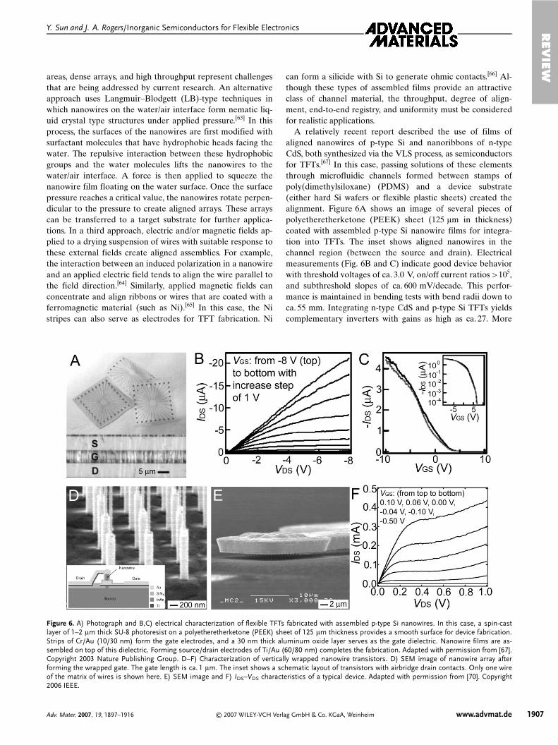
A relatively recent report described the use of films ofaligned nanowires of p-type Si and nanoribbons of n-typeCdS, both synthesized via the VLS process, as semiconductorsfor TFTs.[67] In this case, passing solutions of these elementsthrough microfluidic channels formed between stamps ofpoly(dimethylsiloxane) (PDMS) and a device substrate(either hard Si wafers or flexible plastic sheets) created thealignment. Figure 6A shows an image of several pieces ofpolyetheretherketone (PEEK) sheet (125 lm in thickness)coated with assembled p-type Si nanowire films for integra-tion into TFTs. The inset shows aligned nanowires in thechannel region (between the source and drain). Electricalmeasurements (Fig. 6B and C) indicate good device behaviorwith threshold voltages of ca. 3.0 V, on/off current ratios > 105,and subthreshold slopes of ca. 600 mV/decade. This perfor-mance is maintained in bending tests with bend radii down toca. 55 mm. Integrating n-type CdS and p-type Si TFTs yieldscomplementary inverters with gains as high as ca. 27. More
REV
IEWY. Sun and J. A. Rogers/Inorganic Semiconductors for Flexible Electronics
Adv. Mater. 2007, 19, 1897–1916 © 2007 WILEY-VCH Verlag GmbH & Co. KGaA, Weinheim www.advmat.de 1907
Figure 6. A) Photograph and B,C) electrical characterization of flexible TFTs fabricated with assembled p-type Si nanowires. In this case, a spin-castlayer of 1–2 lm thick SU-8 photoresist on a polyetheretherketone (PEEK) sheet of 125 lm thickness provides a smooth surface for device fabrication.Strips of Cr/Au (10/30 nm) form the gate electrodes, and a 30 nm thick aluminum oxide layer serves as the gate dielectric. Nanowire films are as-sembled on top of this dielectric. Forming source/drain electrodes of Ti/Au (60/80 nm) completes the fabrication. Adapted with permission from [67].Copyright 2003 Nature Publishing Group. D–F) Characterization of vertically wrapped nanowire transistors. D) SEM image of nanowire array afterforming the wrapped gate. The gate length is ca. 1 lm. The inset shows a schematic layout of transistors with airbridge drain contacts. Only one wireof the matrix of wires is shown here. E) SEM image and F) IDS–VDS characteristics of a typical device. Adapted with permission from [70]. Copyright2006 IEEE.

complex circuits, such as five-stage ring oscillators fabricatedwith p-type Si nanowire films on glass substrates and with os-cillation frequencies of up to 11.7 MHz (at supply voltages of43 V), can be achieved with this approach.[68] Although theper-wire mobilities can be high (> 100 cm2 V–1 s–1), a disadvan-tage of these types of devices is their relatively low level ofoutput current per width (determined from the physical di-mensions of the devices), which results from the low to mod-erate coverage (ca. 3–4 %) of nanowires in the channel andtheir uncontrolled end-to-end registration.
Current levels from nanowire array transistors can be in-creased by using designs, such as vertical wrap-gated layouts,in which the coverage and registration can be greatly in-creased compared with the arrays shown in Figure 6A. De-vices that use arrays of InAs nanowires with 80 nm diameters(defined by the size of lithographically patterned Au disks)grown epitaxially on appropriate substrates in a chemical-beam-epitaxy (CBE) system represent one example of thistype of design.[69] These nanowires can be integrated intotransistors (metal-insulator-semiconductor field-effect transis-tors (MISFETs)), shown in the inset of Figure 6D, by suitableprocessing. The sequence begins with deposition of 60 nmSiNx as the insulating layer. Sputtering yields a conformal bi-layer of Ti/Au for the gate electrode. Exposing the top por-tions of the wires by wet-etching creates the structure in Fig-ure 6D. Optical lithography and wet-etching define the gatepads and gate fingers. The fabrication ends with the formationof the drain electrode, connected to the wrapped metal layersaround the top portions of the wires by use of an air-bridgetechnology.[70] Figure 6E shows an SEM image of a typicaltransistor that incorporates ca. 40 nanowires (i.e., the totalcross-sectional area of the channel is ca. 0.2 lm2, with a corre-sponding coverage of only ca. 0.6 %). The wire coverage canbe increased by increasing the density of the patterned cata-lysts (e.g., Au disks), resulting in further increases in current.The wafer growth substrate serves as the source electrode.Figure 6F presents the electrical response, which indicatesn-type operation in depletion mode. An estimate of the mo-bility, based on models[71] traditionally used for nanowiretransistors, yields ca. 3000 cm2 V–1 s–1. Although this verticalgeometry naturally incorporates aligned nanowires with goodend-to-end registration, integration for the types of macro-electronics applications discussed here requires further devel-opment.
6. Films of Nano-/Microstructures Formed FromHigh-Quality Wafers
Single-crystal semiconductor wafers represent exceedinglywell-developed forms of materials technology that are, at thesame time, commodity items owing to their widespread use inconventional electronics and optoelectronics. The high levelsof purity, surface smoothness, the control over crystallinity,doping concentration and type, and the resulting high carriermobilities match or exceed those that are possible with cur-
rent versions of growth techniques for films, nanowires, nano-particles, or nanoribbons. Nanometer- and micrometer-scalestructures—e.g., wires, ribbons, platelets, disks, membranes—fabricated from high-quality, bulk wafers can, as a result, pro-vide useful building blocks for high-performance TFTs. Thisapproach was first reported in 2004,[72] and significant ad-vances have been achieved since that time.[73–79] This sectiondiscusses some aspects of approaches for generating suchstructures from bulk wafers and for printing them onto plasticand other substrates. Flexible TFTs and simple circuits fabri-cated with these printed elements provide examples of thelevels of performance that can be achieved.
6.1. Fabrication of Nano-/Microstructures
Single-crystalline nano-/microstructures of semiconductorscan be fabricated from conventional wafers (referred to as“mother wafers”) of these materials through so-called “top-down” approaches (as opposed to the chemical synthetic“bottom-up” approaches described in the previous section) inwhich lithographic patterning and etching techniques createthe desired structures from the near-surface portions of themother wafers. Semiconductor elements generated in thismanner inherit the high materials quality of the mother wa-fers, which, in turn, enables excellent electrical properties indevices built with them. Two etching strategies have beenexploited to produce these kinds of structures, as illustrated inFigure 7. The most straightforward approach involves isotro-pic selective etching of sacrificial layers of multilayered wafersto release thin semiconductor structures (see Fig. 7A). Exam-ples include Si structures generated from silicon-on-insulator(SOI) wafers and GaAs structures from GaAs wafers withepitaxial layers of AlAs and GaAs (top surfaces), where litho-graphic steps followed by removal of SiO2
[72–75,80] and AlAs,[81]
respectively, release thin ribbons, platelets, or wires. Figure 7Bshows an SEM image of GaAs ribbons with thicknesses of270 nm, widths of 5 lm, and lengths of up to several centi-meters, indicating their mechanical flexibility, dimensionaluniformity, and surface smoothness.
A different class of approach uses similar lithographic steps,followed by anisotropic etching along certain crystallineplanes to generate ribbons/wires from conventional bulk wa-fers in a manner that avoids the high costs associated with wa-fers that have specialized layered structures. Figure 7C depictsa process for generating Si ribbons from a (111) Si wafer. Thefirst step defines shallow trenches with side walls terminatedin (110) planes by lithography and reactive ion etching (RIE).Coating the top surfaces and parts of the side walls of thetrenches with thin resists of, for example, SiO2, Si3N4, and Aufollowed by etching in KOH, an etchant with high etching se-lectivity along the (110) orientation of single-crystalline Si,generates thin ribbons of Si.[76] Figure 7D presents an SEMimage of structures fabricated in this manner. Thicknesses be-tween several tens and several hundreds of nanometers canbe achieved through appropriate control of the processing pa-
REV
IEW
Y. Sun and J. A. Rogers/Inorganic Semiconductors for Flexible Electronics
1908 www.advmat.de © 2007 WILEY-VCH Verlag GmbH & Co. KGaA, Weinheim Adv. Mater. 2007, 19, 1897–1916

rameters. The newly formed surfaces of the ribbons exhibitrelatively smooth surfaces, that is, surface roughnesses of0.5 nm, as determined by AFM analysis. More interesting,controlled ripple structures can be sculpted on the surfaces ofside walls when the trenches are formed with specialized in-ductively coupled plasma (ICP)-RIE etching procedures. Pro-cessing such wafers according to the steps shown in Figure 7Cproduces large quantities of ribbons in the form of multilayerstacks (Fig. 7E).[82] In a related but simpler process, anisotrop-ic etching that yields reverse mesas (i.e., structures with newlyformed sidewalls that have an acute angle relative to the origi-nal surface of the mother wafer) forms freestanding wires withtriangular cross sections. This approach has been applied toIII–V compound wafers with top (100) surfaces and zincblende face-centered cubic lattices. Figure 7F shows GaAswires formed by anisotropic etching of a GaAs wafer with1H3PO4 (85 wt %)-13H2O2 (30 wt %)-12H2O (V/V/V) withetch mask lines (e.g., photoresist and SiO2) patterned alongthe (01̄1̄) crystallographic direction on the surface of a (100)GaAs wafer.[83] Figure 7G presents an SEM image of GaAswires with widths of ca. 400 nm formed using SiO2 (50 nmthick) as the etching mask. The curved configurations of thewires indicate their excellent mechanical flexibility. Carefulstudies show that roughness (ca. tens of nanometers) on theetched surfaces originates from slight edge roughness and an-gular misorientation of the resist lines together with intrinsicroughness associated with the etching. In many cases, the ac-
tive devices rely only on the top flat sur-faces of the wires, and their perfor-mance is not adversely affected by theroughness on the etched sidewalls.
6.2. Dry Transfer Printing of ArrayedNano-/Microstructures
Nano-/microstructures fabricated viathe top-down procedures of Figure 7can be either dispersed in solvents andthen assembled on desired substratesusing the types of techniques describedin Section 5 or, more effectively, theycan be designed to retain the positionaland orientational order defined by thelithography process through the use ofanchors that tether their ends to theoriginal wafer. These ordered wires/rib-bons can then be transfer printed ontodesired substrates, including plasticsheets, using elastomeric PDMS stampsas transfer elements. Figure 8A illus-trates the steps in this type of printingprocess.[83a,84] First, placing a piece ofPDMS onto the surface of a wafer withpatterned patches of wires/ribbons gen-
erates, through the interaction of generalized adhesionforces,[85] soft, conformal contact. These adhesion forces (orstrong chemical bonds formed with appropriately designedsurface chemistries) bond the semiconductor nano-/micro-structures to the surface of the PDMS (step i). Peeling thePDMS stamp away from the wafer transfers all of the nano-/microstructures to the stamp (step ii), as the structures breakaway from the mother wafer at the anchor points. Placing this“inked” stamp against a plastic substrate coated with a thinlayer of adhesive (e.g., epoxy resins or photocurable poly-mers), activating the adhesive (e.g., curing the polymer), andthen peeling back the stamp completes the printing (step iii).In a related approach, control of the peel rate enables transferwithout adhesives.[86] The printed arrays of semiconductornano-/microstructures can be processed into TFTs throughtraditional photolithography and deposition of other materi-als (e.g., dielectrics and metal electrodes) that are compatiblewith the plastic substrate. If high-temperature processing(e.g., annealing of ohmic contacts for GaAs,[77] doping ofSi,[74] growth of thermal oxides on Si) is required, then thosesteps can be carried out on the wafer before transfer (or evenbefore fabrication of the nano-/microstructures). By repetitiveprinting in a step-and-repeat fashion, it is possible to createdevices that cover areas on the plastic substrate that are muchlarger than the size of the mother wafer (see the right columnof Fig. 8A).[84] A patterned PDMS stamp (e.g., with patternedposts or with patterned surface chemistries) can pick up wires/
REV
IEWY. Sun and J. A. Rogers/Inorganic Semiconductors for Flexible Electronics
Adv. Mater. 2007, 19, 1897–1916 © 2007 WILEY-VCH Verlag GmbH & Co. KGaA, Weinheim www.advmat.de 1909
A C F
Figure 7. Fabrication procedures (A,C,F) that involve the combined use of lithography and wetchemical etching (and dry RIE etching as well) to generate nano-/microstructures of single-crystal-line inorganic semiconductors. SEM images of structures ( B) GaAs ribbons, D,E) Si ribbons,G) GaAs wires with triangular cross sections) fabricated using this approach.

ribbons from selected areas. The remaining nano-/microstruc-tures on the mother wafer can be printed in subsequent steps.Figure 8B shows a PET sheet (15 × 15 cm2) covered with pat-terned patches of Si ribbon arrays, transferred by using an8 × 8 cm2 PDMS stamp multiple times and a mother wafermuch smaller than the PET substrate. PDMS stamps can befabricated with any desired layout by use of soft lithographiccasting and curing procedures.[87] For example, the inset ofFigure 8C shows a pattern of printed Si ribbons that form thetext “DARPA MacroE” constructed using a stamp and a flex-
ible PET substrate. The enlarged image (i.e., theletter ‘A’) shown in Figure 8C indicates the high fi-delity of the printing technique.
6.3. Si TFTs on Plastic Substrates
Printed arrays of single-crystal wires/ribbons canserve as active materials for high-performanceelectronic devices, for which some, all, or none ofthe processing is performed on the mother sub-strate. The ability to separate, in this manner, high-temperature growth and processing from the finaldevice substrate (e.g., low-temperature plastic) is akey feature of this approach. Figure 9A shows anoptical image of a polyimide sheet (with a thick-ness of 25 lm) covered with an array of TFTs fab-ricated with printed Si ribbons (290 nm thick)where the contact-doped regions are defined onthe mother wafer.[75] The adhesive layer for thetransfer is a liquid precursor to polyimide, that is,polyamic acid, which is converted into electronic-grade polyimide by baking. The dielectric materialis SiO2 grown by PECVD at relatively low temper-ature (e.g., ca. 250 °C). Source, drain, and gateelectrodes use Cr/Au (5/100 nm) deposited by elec-tron-beam evaporation. Figure 9B and C show atop- and cross-sectional view of an as-fabricatedSi-ribbon TFT, respectively. These transistors ex-hibit electrical behavior similar to that of similardevices fabricated on the mother wafers. Figure 9Dpresents the source–drain current from a transistorwith channel length (Lc) of 9 lm, a channel over-lap distance (Lo) of 5.5 lm, and a channel width(Wc) of 200 lm as a function of the drain voltage,for different gate voltages. Figure 9E presentstransfer curves from devices with different channellengths. The mobilities extracted from these typesof devices in the linear regimes are as high asca. 500 cm2 V–1 s–1. Figure 9F presents microwavemeasurements on a transistor with Lc = 2 lm,Lo = 1.5 lm, and Wc = 200 lm. The fT isca. 515 MHz, at gate and drain biases of 2 V. Thefrequency is, as expected, highly dependent on Lc
and Lo. Figure 9G compares the measured (filled)and calculated (open) fT values for devices with
different Lc and Lo, indicating reasonable agreement betweenthem (the measurements do not involve de-embedding). Al-though higher-frequency operation is possible by reducing Lc
and/or Lo, this approach is not attractive for many macroelec-tronic systems because it requires high-resolution lithography,which can be difficult to achieve in a cost-effective manner onlarge area, plastic substrates. By contrast, MESFET devicesmade of GaAs wire/ribbons can offer high speeds even withcoarse patterning resolution and limited capacity for overlayregistration, the latter of which is of particular advantage for
REV
IEW
Y. Sun and J. A. Rogers/Inorganic Semiconductors for Flexible Electronics
1910 www.advmat.de © 2007 WILEY-VCH Verlag GmbH & Co. KGaA, Weinheim Adv. Mater. 2007, 19, 1897–1916
Figure 8. A) Schematic illustration of steps for transfer printing nano-/microstruc-tures generated with the procedures of Fig. 7 onto plastic substrates using PDMSstamps with flat (left column) and patterned (right column) surfaces. The continuoussemiconductor layers represent the arrays of wires/ribbons. B,C) Optical images ofthe patterned patches of arrays of silicon ribbons on polyurethane/PET sheets printedwith PDMS stamps through the processes shown in (A). Adapted from [84].

plastic substrates because they often do not show good dimen-sional stability over large areas. The next section discussessuch devices.
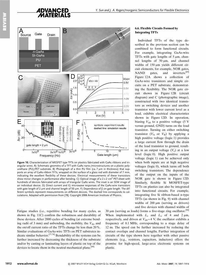
6.4. GaAs TFTs on Plastics
MESFET type TFTs with geometries shown in Figure 10Aon plastic substrates can be fabricated with printed GaAs rib-bons (or wires) that incorporate integrated ohmic contacts.Figure 10B presents an image of a thin polyurethane sheet(with thickness of ca. 7 lm) with an array of TFTs, fabricatedusing GaAs ribbons shown in Figure 7B. Each ribbon consistsof bilayers of 150 nm semi-insulating GaAs (SI-GaAs) and120 nm n-GaAs (carrier concentration 4.0 × 1017 cm–3), onwhich ohmic source–drain electrodes are formed by annealingmetal stacks, that is, 70 nm AuGe/10 nm Ni/70 nm Au, at450 °C for 1 min in an atmosphere of N2. Schottky gate elec-trodes are formed by directly depositing 75 nm Cr/75 nm Au.Wrapping these devices around a glass rod with a diameterof 7 mm indicates their level of flexibility (Fig. 10B). The de-vice performance exhibits only a relatively minor change
(< ≈ 15 %) with bending. In practice, the mechanical fragilityof thin GaAs ribbons (compared to Si ribbons) demands ex-treme care in the transfer printing. TFTs can also be formedwith relatively thick GaAs wires (width of ca. 1–2 lm), whichexhibit higher resistance to fracture.[77,78] Figure 10C shows animage of a 2 × 2 cm2 PET sheet of transistors formed withca. 1.8 lm thick GaAs wires. Each device incorporates 10 par-allel wires, as shown in the inset of Figure 10C. Figure 10Dshows electrical characteristics of a transistor with a gatelength of 2 lm. The response is consistent with n-type deple-tion mode operation of similar MESFETs fabricated on themother wafer. The inset of Figure 10D presents the transfercurves recorded with different gate voltage sweep directions,illustrating the low level of hysteresis. The on/off current ra-tios in the saturated regime (i.e., VDS = 4 V), as evaluatedfrom averaged measurements on many devices, are ca. 106
and the pinch-off voltages in the linear regime (i.e.,VDS = 0.1 V) are –2.7 V. Although the device mobility was notextracted from these data, the value is expected to approachthe intrinsic mobility of GaAs for electrons, that is,ca. 8500 cm2 V–1 s–1.
Microwave measurements can be performed on devices thatuse a layout as shown in the inset of Figure 10E. Each unit ofthe test structure contains two identical TFTs with gatelengths of 2 lm, channel lengths of 50 lm, and channel widthsof 150 lm with a common gate. The corresponding probingpads match the layout of the high-speed probes. The fT is1.55 GHz, consistent with a simple calculated result(1.68 GHz).[78] The gate length, of course, plays an importantrole in determining the operating frequencies of the devices.Figure 10F compares the measured (symbols) and calculated(dashed line) fT values of GaAs-wire TFTs with different gatelengths and channel lengths of 50 lm on PET substrates. Theresults suggest that fT can be increased significantly by reduc-ing the gate length to approach operating frequencies that aresuitable for large active antennas operating in the UHF re-gime, even the S-band.
6.5. Evaluation of the Mechanical Bendability of TFTson Plastics
Good mechanical bendability is a critical feature of many ofthe envisioned applications described in the Introduction. Theflexibility of transistors fabricated with single-crystallinenano-/microstructures (described in sections 6.3 and 6.4) canbe systematically evaluated by squeezing the plastic substrateswith specially designed mechanical stages to generate concave(compressive strains on top device surface) and convex sur-faces (tensile strains; Fig. 11A). Figure 11B shows, as an ex-ample, the variation of the mobility (in the linear regime) of aSi transistor fabricated with Si ribbons on a 25 lm thick poly-imide sheet, normalized by the value in the unbent state, withbending radius and surface strain. The results indicate onlysmall changes in device performance in this range of strains.
REV
IEWY. Sun and J. A. Rogers/Inorganic Semiconductors for Flexible Electronics
Adv. Mater. 2007, 19, 1897–1916 © 2007 WILEY-VCH Verlag GmbH & Co. KGaA, Weinheim www.advmat.de 1911
Figure 9. A–C) Images and D–G) electrical characteristics of transistorsfabricated with Si ribbons on polyimide substrates. PEO stands for theSiO2 layer grown by PECVD. Adapted with permission from [75]. Copy-right 2006 IEEE.
Fatigue studies (i.e., repetitive bending for many cycles, asshown in Fig. 11C) confirm the robustness and durability ofthese devices. After 2000 cycles of bending (at extreme bend-ing radii of 3 mm) and unbending, the mobility, the Vth, andthe on/off current ratio of the TFTs change by less than 20 %.Similar evaluations of GaAs-wire TFTs on PET substrates in-dicate similar behavior.[77,78] Bendability of the systems can befurther increased by decreasing the thickness of the substrateand/or by casting or laminating layers of plastic on top of thedevices to locate them in the neutral mechanical plane.[88]
6.6. Flexible Circuits Formed byIntegrating TFTs
Individual TFTs of the type de-scribed in the previous section can becombined to form functional circuits.For example, integrating GaAs-wireTFTs with gate lengths of 5 lm, chan-nel lengths of 50 lm, and channelwidths of 150 lm yields different cir-cuit elements, for example, NOR gates,NAND gates, and inverters.[89]
Figure 12A shows a collection ofGaAs-wire transistors and simple cir-cuits on a PET substrate, demonstrat-ing the flexibility. The NOR gate cir-cuit shown in Figure 12B (circuitdiagram) and C (photographic image),constructed with two identical transis-tors as switching devices and anothertransistor with lower current level as aload, exhibits electrical characteristicsshown in Figure 12D. In operation,biasing Vdd to a positive voltage (5 Vversus ground, GND) turns on the loadtransistor. Turning on either switchingtransistor (VA or VB) by applying ahigh positive voltage (logic 1) providesa large current flow through the drainof the load transistor to ground, result-ing in an output voltage (Vo) at a lowlevel (logic 0). High positive outputvoltage (logic 1) can be achieved onlywhen both inputs are at high negativevoltages (logic 0), which turns off bothswitching transistors. The dependenceof the output on the inputs of theNOR gate is shown in Figure 12D.Similarly, flexible Si MOSFET-typeTFTs on plastics can also be integratedinto functional circuits. For example,integrating five Si ribbon-based n-typeTFTs (as shown in Fig. 9) with channelwidths of 200 lm (serving as drivers)and five devices with channel widths of
30 lm (serving as loads) forms a five-stage ring oscillator.[90]
When implemented with Lc and Lo of 4 and 2 lm,respectively, and driven at Vdd = 4 V, the oscillator exhibits afrequency of 8.1 MHz, corresponding to a stage delay of12 ns. The speed can be further increased by reducing thecontact overlaps and channel lengths. Further integration ofcircuits of the type shown here together with other passiveelements (e.g., resistors, capacitors, inductors) offers thepromise for high-speed, large-area electronic systems onplastic.
REV
IEW
Y. Sun and J. A. Rogers/Inorganic Semiconductors for Flexible Electronics
1912 www.advmat.de © 2007 WILEY-VCH Verlag GmbH & Co. KGaA, Weinheim Adv. Mater. 2007, 19, 1897–1916
Figure 10. Characterization of MESFET type TFTs on plastics fabricated with GaAs ribbons and tri-angular wires. A) Schematic geometry of a TFT with GaAs nano-/microstructures on a plastic poly-urethane (PU)/PET substrate. B) Photograph of a thin PU film (ca. 7 lm in thickness) that sup-ports an array of GaAs-ribbon TFTs, wrapped on the surface of a glass rod with diameter of 7 mm,indicating the excellent flexibility of these devices. Electrical measurements of these transistorsshow minor changes in performance after bending. C) Optical image of a 2 × 2 cm2 PET sheet withhundreds of devices fabricated with arrays of triangular GaAs wires. The inset is an SEM image ofan individual device. D) Direct current and E) microwave responses of the GaAs-wire transistorswith gate length of 2 lm and channel length of 50 lm. F) Dependence of fT on gate length. The dif-ferent symbols represent measurements on different devices. The dashed line corresponds to cal-culations. Adapted with permission from [78]. Copyright 2006 American Institute of Physics.

7. Conclusion and Outlook
As outlined in this Review, a variety of inorganic materialsin the form of amorphous, nanocrystalline, microcrystalline,and polycrystalline thin films as well as assembled arrays ofnanowires/nanoribbons and nano-/microstructures can yieldtransistors with high mobilities and simple circuit componentswith good performance. Many of these materials have the po-tential to be grown and processed on low-temperature plasticsubstrates, and in several cases these capabilities have alreadybeen demonstrated. TFTs fabricated with inorganic materialson plastics can be operated at high frequencies,[25,75,78] into theultrahigh frequency (UHF) and S-band regimes, allowingthem, in principle, to be applied in demanding applications,such as radio frequency communications. In addition, new
properties, such as transparency, can be introduced with mate-rials such as the transparent oxides (see section 3), therebycreating new types of application possibilities. Future workwill, we believe, focus on the further development of thesematerials and methods for incorporating them into realisticapplications. Issues related to mechanical and electrical prop-erties of interfaces and, in particular, to the semiconductor/di-electric interfaces will be important.
Alternative approaches to these systems involve organicelectronic materials, including newer systems such as films ofsingle-walled carbon nanotubes, and directed assembly of pre-formed circuit blocks. Small-molecule and polymer-based or-ganic semiconductors have the advantage that they are morefully explored for electronic applications than some of the in-organic approaches presented here (e.g., nanowires, nanocrys-tals), but the modest performance that has, thus far, been pos-sible with them limits the range of applications. Carbonnanotube films, on the other hand, can offer extremely highperformance[91–94] and also optical transparency;[95] in additionthey have the advantage that they are chemically and me-chanically robust compared to most conventional organics. Asa result, this class of material appears to have some promise
REV
IEWY. Sun and J. A. Rogers/Inorganic Semiconductors for Flexible Electronics
Adv. Mater. 2007, 19, 1897–1916 © 2007 WILEY-VCH Verlag GmbH & Co. KGaA, Weinheim www.advmat.de 1913
Figure 11. Mechanical characterization of Si ribbon based transistors onpolyimide substrates (with thickness of 25 lm). The normalized mobility(ldevice/ldevice
0) is plotted as a function of bending-induced strain andbending radius. Adapted with permission from [75]. Copyright 2006 IEEE.
Figure 12. A) Optical image of a bent PET substrate with GaAs-wirebased TFTs and various circuits fabricated with these TFTs and GaAsbased diodes. B) Circuit diagram, C) optical image, and D) output–inputcharacteristic of a NOR gate fabricated with three TFTs. The load transis-tor (top in C) has a channel length of 100 lm, while the switching tran-sistors (bottom in C) have channel lengths of 50 lm. The gate lengths ofall transistors are 5 lm. Each transistor comprises 10 aligned GaAs wireswith width of ca. 2 lm. Vdd applied to the NOR gate was 5 V vs. ground(GND). The logic inputs of “0” and “1” were driven by –5 and 2 V, re-spectively. The logic “0” and “1” outputs were 1.58–1.67 and 4.1 V, re-spectively. Reproduced from [89].

for macroelectronics. Another route to this type of electronicsuses guided fluidic self-assembly of preformed circuitblocks.[96–98] An attractive attribute of this approach is that itexploits fully, well-developed silicon wafer-based circuit tech-nologies. Reaching yields that are high enough to supportapplications in, for example, information display is challeng-ing. Also, the reliability of interconnects and the mechanicalintegrity of the interfaces between the circuit blocks and thesurrounding material (i.e., adhesives) are uncertain. The ad-vantages and disadvantages of these very different approachesmake it difficult to identify a clearly preferred path. Neverthe-less, the large number of promising approaches that alreadyexist leads one to be optimistic that low cost, large area, highperformance flexible electronics will mature into an impor-tant technology with wide-ranging applications.
Received: September 19, 2006Published online: July 12, 2007
Noted added in proof: After this Review was submitted, twopapers with direct relevance to the topic were published. Newtypes of flexible transparent TFTs (related to Section 3) werereported with the use of assembled nanowires of In2O3 andZnO on plastic substrates combined with thin layers of high-kAl2O3 (formed via atomic layer deposition (ALD)). Typicaltransistors made of In2O3 nanowires on PET sheets exhibitedmobilities of 120–167 cm2 V–1 s–1.[99] TFTs made of single-crystal Si membranes on PEY substrates were reported to ex-hibit fT of 1.9 GHz. These devices have similar fabricationresolution to those reported in [75] (Section 6.3) and specialdevice layouts, such as p-shape, two-finger gates.[100]
–[1] a) Special issue on “Macroelectronics”, Mater. Res. Soc. Bull. 2006,
31 (6), 447–475. b) Special issue on “Flexible Electronics”, Mater.Today 2006, 9 (4), 24–52. c) Special issue on “Flexible ElectronicsTechnology, Part 1: Systems and Applications”, Proc. IEEE 2005,93 (7), 1235–1382. d) Special issue on “Flexible Electronics Technol-ogy, Part 2: Materials and Devices”, Proc. IEEE 2005, 93 (8),1391–1513.
[2] a) R. H. Reuss, B. R. Chalamala, A. Moussessian, M. G. Kane,A. Kumar, D. C. Zhang, J. A. Rogers, M. Hatalis, D. Temple,G. Moddel, B. J. Eliasson, M. J. Estes, J. Kunze, E. S. Handy, E. S.Harmon, D. B. Salzman, J. M. Woodall, M. A. Alam, J. Y. Murthy,S. C. Jacobsen, M. Olivier, D. Markus, P. M. Campbell, E. Snow,Proc. IEEE 2005, 93, 1239. b) T. Someya, T. Sekitani, S. Iba, Y. Kato,H. Kawaguchi, T. Sakurai, Proc. Natl. Acad. Sci. USA 2004, 101,9966. c) J. A. Rogers, Z. Bao, K. Baldwin, A. Dodabalapur, B. Crone,V. R. Raju, V. Kuck, H. Katz, K. Amundson, J. Ewing, P. Drzaic,Proc. Natl. Acad. Sci. USA 2001, 98, 4835. d) S. R. Forrest, Nature2004, 428, 911.
[3] a) G. H. Gelinck, H. E. A. Huitema, E. van Veedendaal, E. Canta-tore, L. Schrijnemakers, J. B. P. H. van der Putten, T. C. T. Geuns,M. Beenhakkers, J. B. Giesbers, B.-H. Huisman, E. J. Meijer, E. M.Benito, F. J. Touwslager, A. W. Marsman, B. J. E. van Rens, D. M.de Leeuw, Nat. Mater. 2004, 3, 106. b) Y. Chen, J. Au, P. Kazlas,A. Ritenour, H. Gates, M. McCreaey, Nature 2003, 423, 136.c) A. Nathan, B. Park, A. Sazonov, D. Tao, I. Chan, P. Servati,K. Karim, T. Charania, D. Striakhilev, Q. Ma, R. V. R. Murthy,Microelectron. J. 2000, 31, 883.
[4] a) M. Troccoli, T. Afentakis, M. K. Hatalis, A. T. Voutsas, M. Ada-chi, J. W. Hartzell, Mater. Res. Soc. Symp. Proc. 2003, 769, 93.b) T. Afentakis, M. K. Hatalis, A. T. Voutsas, J. W. Hartzell, Mater.Res. Soc. Symp. Proc. 2003, 769, 47. c) J. H. Cheon, J. H. Choi, J. H.Hur, J. Jang, H. S. Shim, J. K. Jeong, Y. G. Mo, H. K. Chung, IEEETrans. Electron Devices 2006, 53, 1273.
[5] J. A. Rogers, Science 2001, 291, 1502.[6] a) F. Eder, H. Klauk, M. Halik, U. Zschieschang, G. Schmid,
C. Dehm, Appl. Phys. Lett. 2004, 84, 2673. b) Y.-H. Kim, D.-G.Moon, J.-I. Han, IEEE Electron Device Lett. 2004, 25, 702.c) B. Lamprecht, R. Thünauer, M. Ostermann, G. Jakopic, G. Leis-ing, Phys. Status Solidi A 2002, 202 (5), R50.
[7] a) D. Voss, Nature 2000, 407, 442. b) W. Clemens, W. Fix, J. Ficker,A. Knobloch, A. Ullmann, J. Mater. Res. 2004, 19, 1963. c) M. Chen,Proc. IEEE 2005, 93, 1339. d) K. Cheng, M.-H. Yang, W. W. W.Chiu, C.-Y. Huang, J. Chang, T.-F. Ying, Y. Yang, Macromol. RapidCommun. 2005, 26, 247.
[8] V. C. Sundar, J. Zaumseil, V. Podzorov, E. Menard, R. L. Willett,T. Someya, M. E. Gershenson, J. A. Rogers, Science 2004, 303, 1644.
[9] a) A. L. Briseno, R. J. Tseng, M.-M. Ling, E. H. L. Falcao, Y. Yang,F. Wudl, Z. Bao, Adv. Mater. 2006, 18, 2320. b) R. Zeis, C. Besnard,T. Siegrist, C. Schlockermann, X. Chi, C. Kloc, Chem. Mater. 2006,18, 244. c) R. Zeis, T. Siegrist, Ch. Kloc, Appl. Phys. Lett. 2005, 86,022 103. d) R. W. I. de Boer, M. E. Gershenson, A. F. Morpurgo,V. Podzorov, Phys. Status Solidi A 2004, 201, 1302. e) I. N. Hulea,S. Russo, A. Molinari, A. F. Morpurgo, Appl. Phys. Lett. 2006, 88,113 512.
[10] R. F. Service, Science 2006, 312, 1593.[11] a) P. Servati, A. Nathan, Proc. IEEE 2005, 93, 1257. b) E. Fortunato,
L. Pereira, H. Águas, I. Ferreira, R. Martins, Proc. IEEE 2005, 93,1281. c) A. Sazonov, D. Striakhilev, C.-H. Lee, A. Nathan, Proc.IEEE 2005, 93, 1420. d) L. Zhou, S. Jung, E. Brandon, T. N. Jackson,IEEE Trans. Electron Devices 2006, 53, 380. e) P. I. Hsu, H. Glesko-va, M. Huang, Z. Suo, S. Wagner, J. C. Sturm, J. Non-Cryst. Solids2002, 299–302, 1355. f) C.-S. Yang, L. L. Smith, C. B. Arthur, G. N.Parsons, J. Vac. Sci. Technol., B 2000, 18, 683. g) L. A. MacQueen,J. Zikovsky, G. Dennler, M. Latreche, G. Czeremuszkin, M. R.Wertheimer, Plasma Processes Polym. 2006, 3, 58.
[12] A. Sazonov, C. McArthur, J. Vac. Sci. Technol., A 2004, 22, 2052.[13] P. Alpuim, V. Chu, J. P. Conde, J. Vac. Sci. Technol., A 2003, 21, 1048.[14] I.-C. Cheng, S. Wagner, Appl. Phys. Lett. 2002, 80, 440.[15] C.-H. Lee, A. Sazonov, A. Nathan, Appl. Phys. Lett. 2005, 86,
222 106.[16] A. J. Flewitt, W. I. Milne, Proc. IEEE 2005, 93, 1364.[17] a) J. P. Conde, P. Alpuim, M. Boucinha, J. Gaspar, V. Chu, Thin Sol-
id Films 2001, 395, 105. b) P. Alpuim, V. Chu, J. P. Conde, J. Non-Cryst. Solids 2000, 266–269, 110. c) P. Alpuim, V. Chu, J. P. Conde, J.Appl. Phys. 1999, 86, 3812. d) P. Alpuim, V. Chu, J. P. Conde, J. Vac.Sci. Technol., A 2001, 19, 2328. e) M. Härting, D. T. Britton,D. Knoesen, W. Egger, Appl. Surf. Sci. 2006, 252, 3188.
[18] J. P. Conde, P. Alpuim, V. Chu, Thin Solid Films 2003, 430, 240.[19] P. C. van der Wilt, M. G. Kane, A. B. Limanov, A. H. Firester,
L. Goodman, J. Lee, J. R. Abelson, A. M. Chitu, J. S. Im, MRS Bull.2006, 31, 461.
[20] a) M. Wu, K. Pangal, J. C. Sturm, S. Wagner, Appl. Phys. Lett. 1999,75, 2244. b) M. Wu, S. Wagner, Appl. Surf. Sci. 2001, 175–176, 753.c) M. Wu, S. Wagner, Appl. Phys. Lett. 2001, 78, 3729. d) M. Wu,S. Wagner, J. Non-Cryst. Solids 2002, 299–302, 1316. e) M. Wu, X.-Z.Bo, J. C. Sturm, S. Wagner, IEEE Trans. Electron Devices 2002, 49,1993.
[21] a) E.-S. Hwang, Y.-J. Kim, B.-K. Ju, Sens. Actuators, A 2004, 111,135. b) Y. Lee, H. Li, S. J. Fonash, IEEE Electron Device Lett. 2003,24, 19.
[22] a) D. J. McCulloch, S. D. Brotherton, Appl. Phys. Lett. 1995, 66,2060. b) A. Imparato, C. Minarini, A. Rubino, P. Tassini, F. Villani,D. D. Sala, E. Amendola, M. Kunst, H.-C. Neitzert, S. Bellone, Thin
REV
IEW
Y. Sun and J. A. Rogers/Inorganic Semiconductors for Flexible Electronics
1914 www.advmat.de © 2007 WILEY-VCH Verlag GmbH & Co. KGaA, Weinheim Adv. Mater. 2007, 19, 1897–1916
Solid Films 2005, 487, 58. c) T. Sameshima, M. Hara, S. Usui, Jpn. J.Appl. Phys. Part 1 1989, 28, 1789. d) J. S. Im, H. J. Kim, M. O.Thompson, Appl. Phys. Lett. 1993, 63, 1969.
[23] a) H. J. Kahlert, B. Burghardt, F. Simon, M. Stopka, Proc. SPIE-Int.Soc. Opt. Eng. 2003, 5004, 20. b) C. W. Kim, K. C. Moon, H. J. Kim,K. C. Park, C. H. Kim, I. G. Kim, C. M. Kim, S. Y. Joo, J. K. Kang,U. J. Chung, Dig. Tech. Pap.—Soc. Inf. Disp. Int. Symp. 2004, 35, 868.c) A. T. Voutsas, IEEE Trans. Electron Devices 2003, 50, 1494.
[24] a) J. S. Im, R. S. Sposili, M. A. Crowder, Appl. Phys. Lett. 1997, 70,3434. b) S. D. Brotherton, M. A. Crowder, A. B. Limanov, B. A.Turk, J. S. Im, in SID Conf. Rec. 21st Int. Display Res. Conf., Societyfor Information Display, San Jose, CA 2001, p. 387.
[25] M. G. Kane, L. Goodman, A. H. Firester, P. C. van der Wilt, A. B.Limanov, J. S. Im, in Tech. Dig.—Int. Electron Device Meeting,IEEE, Piscataway, NJ 2005, p. 939.
[26] M. N. Troccoli, A. J. Roudbari, T.-K. Chuang, M. K. Hatalis, Solid-State Electron. 2006, 50, 1080.
[27] T. Shimoda, Y. Matsuki, M. Furusawa, T. Aoki, I. Yudasaka, H. Ta-naka, H. Iwasawa, D. Wang, M. Miyasaka, Y. Takeuchi, Nature 2006,440, 783.
[28] a) E. M. C. Fortunato, P. M. C. Barquinha, A. C. M. B. G. Pimentel,A. M. F. Gonçalves, A. J. S. Pereira, Appl. Phys. Lett. 2004, 85, 2541.b) A. Pimentel, E. Fortunato, A. Gonçalves, A. Marques, H. Águas,L. Pereira, I. Ferreira, R. Martins, Thin Solid Films 2005, 487, 212.c) P. F. Carcia, R. S. McLean, M. H. Reilly, G. Nunes, Jr., Appl.Phys. Lett. 2003, 82, 1117.
[29] I.-D. Kim, Y. Choi, H. L. Tuller, Appl. Phys. Lett. 2005, 87, 043 509.[30] E. Fortunato, P. Barquinha, A. Pimentel, A. Gonçalves, A. Marques,
L. Pereira, R. Martins, Thin Solid Films 2005, 487, 205.[31] S. Ju, K. Lee, D. B. Janes, M.-H. Yoon, A. Facchetti, T. J. Marks,
Nano Lett. 2005, 5, 2281.[32] E. Fortunato, A. Pimentel, L. Pereira, A. Gonçalves, G. Lavareda,
H. Águas, I. Ferreira, C. N. Carvalho, R. Martins, J. Non-Cryst. Sol-ids 2004, 338–340, 806.
[33] P. Barquinha, E. Fortunato, A. Gonçalves, A. Pimentel, A. Marques,L. Pereira, R. Martins, Superlattices Microstruct. 2006, 39, 319.
[34] K.-K. Kim, H.-S. Kim, D.-K. Hwang, J.-H. Lim, S.-J. Park, Appl.Phys. Lett. 2003, 83, 63.
[35] D. C. Look, G. M. Renlund, R. H. Burgener, II, J. R. Sizelove, Appl.Phys. Lett. 2004, 85, 5269.
[36] M. Matsumura, R. P. Camata, Thin Solid Films 2005, 476, 317.[37] a) W. J. E. Beek, M. M. Wienk, R. A. J. Janssen, Adv. Mater. 2004,
16, 1009. b) C. Pacholski, A. Kornowski, H. Weller, Angew. Chem.Int. Ed. 2002, 41, 1188.
[38] a) L. E. Greene, M. Law, J. Goldberger, F. Kim, J. C. Johnson,Y. Zhang, R. J. Saykally, P. Yang, Angew. Chem. Int. Ed. 2003, 42,3031. b) P. Yang, H. Yan, S. Mao, R. Russo, J. Johnson, R. Saykally,N. Morris, J. Pham, R. He, H.-J. Choi, Adv. Funct. Mater. 2002, 12,323. c) Z. L. Wang, J. Phys. Condens. Matter 2004, 16, R829.d) Z. W. Pan, Z. R. Dai, Z. L. Wang, Science 2001, 291, 1947.e) H. J. Fan, P. Werner, M. Zacharias, Small 2006, 2, 700.
[39] B. Sun, H. Sirringhaus, Nano Lett. 2005, 5, 2408.[40] a) K. Nomura, H. Ohta, K. Ueda, T. Kamiya, M. Hirano, H. Hosono,
Science 2003, 300, 1269. b) K. Nomura, H. Ohta, K. Ueda, T. Ka-miya, M. Orita, M. Hirano, T. Suziki, C. Honjyo, Y. Hosono, J. Appl.Phys. 2004, 95, 5532. c) K. Nomura, T. Kamiya, H. Ohta, K. Ueda,M. Hirano, H. Hosono, Appl. Phys. Lett. 2004, 85, 1993.
[41] a) K. Nomura, A. Takagi, T. Kamiya, H. Ohta, M. Hirano, H. Hoso-no, Jpn. J. Appl. Phys. Part 1 2006, 45, 4303. b) K. Nomura, H. Ohta,A. Takagi, T. Kamiya, M. Hirano, H. Hosono, Nature 2004, 432, 488.
[42] R. E. Presley, D. Hong, H. Q. Chiang, C. M. Hung, R. L. Hoffman,J. F. Wager, Solid-State Electronics 2006, 50, 500.
[43] S. Narushima, M. Orita, M. Hirano, H. Hosono, Phys. Rev. B 2002,66, 035 203.
[44] P. Görrn, M. Sander, J. Meyer, M. Kröger, E. Becker, H.-H. Jo-hannes, W. Kowalsky, T. Riedl, Adv. Mater. 2006, 18, 738.
[45] L. Wang, M.-H. Yoon, G. Lu, Y. Yang, A. Facchetti, T. J. Marks, Nat.Mater. 2006, 5, 893.
[46] P. K. Weimer, Proc. IRE 1962, 50, 1462.[47] a) T. P. Brody, J. A. Asars, G. D. Dixon, IEEE Trans. Electron De-
vices 1973, 20, 995. b) T. P. Brody, IEEE Trans. Electron Devices 1984,31, 1614. c) T. P. Brody, Proc. SPIE-Int. Soc. Opt. Eng. 1992, 1664, 2.
[48] B. A. Ridley, B. Nivi, J. M. Jacobson, Science 1999, 286, 746.[49] A. Van Calster, A. Vervaet, I. De Rycke, J. De Baets, J. Vanfleteren,
J. Cryst. Growth 1988, 86, 924.[50] D. V. Talapin, C. B. Murray, Science 2005, 310, 86.[51] a) C. P. Collier, R. J. Saykally, J. J. Shiang, S. E. Henrichs, J. R.
Heath, Science 1997, 277, 1978. b) N. F. Mott, Conduction in Non-Crystalline Materials, 2nd ed., Clarendon, Oxford, UK 1993.
[52] C. Klinke, J. Chen, A. Afzali, Ph. Avouris, Nano Lett. 2005, 5, 555.[53] D. B. Mitzi, J. Mater. Chem. 2004, 14, 2355.[54] D. B. Mitzi, L. L. Kosbar, C. E. Murray, M. Copel, A. Afzali, Nature
2004, 428, 299.[55] D. B. Mitzi, M. Copel, S. J. Chey, Adv. Mater. 2005, 17, 1285.[56] D. J. Milliron, D. B. Mitzi, M. Copel, C. E. Murray, Chem. Mater.
2006, 18, 587.[57] a) G. Zheng, W. Lu, S. Jin, C. M. Lieber, Adv. Mater. 2004, 16, 1890.
b) Y. Cui, Z. Zhong, D. Wang, W. Wang, C. M. Lieber, Nano Lett.2003, 3, 149.
[58] X. Duan, C. M. Lieber, Adv. Mater. 2000, 12, 298.[59] a) H. Yu, W. E. Buhro, Adv. Mater. 2003, 15, 416. b) F. M. Davidson,
III, A. D. Schricker, R. J. Wiacek, B. A. Korgel, Adv. Mater. 2004,16, 646.
[60] a) Y. Xia, P. Yang, Y. Sun, Y. Wu, B. Mayers, B. Gates, Y. Yin,F. Kim, H. Yan, Adv. Mater. 2003, 15, 353. b) C. M. Lieber, SolidState Commun. 1998, 107, 607. c) M. Law, J. Goldberger, P. Yang,Annu. Rev. Mater. Res. 2004, 34, 83. d) Z. R. Dai, Z. W. Pan, Z. L.Wang, Adv. Funct. Mater. 2003, 13, 9. e) Nanowires and Nanobelts:Materials, Properties and Devices; Vols. I,II (Ed: Z. L. Wang),Kluwer Academic, Boston, MA 2003.
[61] Y. Shan, K. Kalkan, C.-Y. Peng, S. J. Fonash, Nano Lett. 2004, 4,2085.
[62] Y. Huang, X. Duan, Q. Wei, C. M. Lieber, Science 2001, 291, 630.[63] a) D. Whang, S. Jin, Y. Wu, C. M. Lieber, Nano Lett. 2003, 3, 1255.
b) A. Tao, F. Kim, C. Hess, J. Goldberger, R. He, Y. Sun, Y. Xia,P. Yang, Nano Lett. 2003, 3, 1229.
[64] a) P. A. Smith, C. D. Nordquist, T. N. Jackson, T. S. Mayer, B. R.Martin, J. Mbindyo, T. E. Mallouk, Appl. Phys. Lett. 2000, 77, 1399.b) X. Duan, Y. Huang, Y. Cui, J. Wang, C. M. Lieber, Nature 2001,409, 66.
[65] A. K. Bentley, J. S. Trethewey, A. B. Ellis, W. C. Crone, Nano Lett.2004, 4, 487.
[66] Y. Wu, J. Xinag, C. Yang, W. Lu, C. M. Lieber, Nature 2004, 430, 61.[67] X. Duan, C. Niu, V. Sahi, J. Chen, J. W. Parce, S. Empedocles,
J. Goldman, Nature 2003, 425, 274.[68] R. S. Friedman, M. C. McAlpine, D. S. Ricketts, D. Ham, C. M. Lie-
ber, Nature 2005, 434, 1085.[69] T. Bryllert, L.-E. Wernersson, T. Löwgren, L. Samuelson, Nanotech-
nology 2006, 17, S227.[70] T. Bryllert, L.-E. Wernersson, L. E. Fröberg, L. Samuelson, IEEE
Electron Device Lett. 2006, 27, 323.[71] Y. Huang, X. Duan, Y. Cui, C. M. Lieber, Nano Lett. 2002, 2, 101.[72] E. Menard, K. J. Lee, D.-Y. Khang, R. G. Nuzzo, J. A. Rogers, Appl.
Phys. Lett. 2004, 84, 5398.[73] E. Menard, R. G. Nuzzo, J. A. Rogers, Appl. Phys. Lett. 2005, 86,
093 507.[74] Z.-T. Zhu, E. Menard, K. Hurley, R. G. Nuzzo, J. A. Rogers, Appl.
Phys. Lett. 2005, 86, 133 507.[75] J.-H. Ahn, H.-S. Kim, K. J. Lee, Z. Zhu, E. Menard, R. G. Nuzzo,
J. A. Rogers, IEEE Electron Device Lett. 2006, 27, 460.[76] S. Mack, M. A. Meitl, A. J. Baca, Z.-T. Zhu, J. A. Rogers, Appl.
Phys. Lett. 2006, 88, 213 101.
REV
IEWY. Sun and J. A. Rogers/Inorganic Semiconductors for Flexible Electronics
Adv. Mater. 2007, 19, 1897–1916 © 2007 WILEY-VCH Verlag GmbH & Co. KGaA, Weinheim www.advmat.de 1915

[77] Y. Sun, S. Kim, I. Adesida, J. A. Rogers, Appl. Phys. Lett. 2005, 87,083 501.
[78] Y. Sun, E. Menard, J. A. Rogers, H.-S. Kim, S. Kim, G. Chen, I. Ade-sida, R. Dettmer, R. Cortez, A. Tewksbury, Appl. Phys. Lett. 2006,88, 183 509.
[79] a) H.-C. Yuan, Z. Ma, M. M. Roberts, D. E. Savage, M. G. Lagally,J. Appl. Phys. 2006, 100, 013 708. b) H. Y. Li, L. H. Guo, W. Y. Loh,L. K. Bera, Q. X. Zhang, N. Hwang, E. B. Liao, K. W. Teoh, H. M.Chua, Z. X. Shen, C. K. Cheng, G. Q. Li, D.-L. Kwong, IEEE Elec-tron Device Lett. 2006, 27, 538.
[80] Y. Yin, B. Gates, Y. Xia, Adv. Mater. 2000, 12, 1426.[81] a) W. K. Chan, D. M. Shah, T. J. Gmitter, C. Caneau, Electron. Lett.
1992, 28, 708. b) D. M. Shah, W. K. Chan, T. J. Gmitter, L. T. Florez,H. Schumacher, B. P. Van Der Gaag, Electron. Lett. 1990, 26, 1865.c) E. Yablonovitch, T. Gmitter, J. P. Harbison, R. Bhat, Appl. Phys.Lett. 1987, 51, 2222. d) Y. Sun, V. Kumar, I. Adesida, J. A. Rogers,Adv. Mater. 2006, 18, 2857.
[82] H. C. Ko, A. J. Baca, J. A. Rogers, Nano Lett. 2006, 6, 2318[83] a) Y. Sun, J. A. Rogers, Nano Lett. 2004, 4, 1953. b) Y. Sun, D.-Y.
Khang, F. Hua, K. Hurley, R. G. Nuzzo, J. A. Rogers, Adv. Funct.Mater. 2005, 15, 30. c) Y. Sun, R. A. Graff, M. S. Strano, J. A. Ro-gers, Small 2005, 1, 1052.
[84] K. J. Lee, M. J. Motala, M. A. Meitl, W. R. Childs, E. Menard, A. K.Shim, J. A. Rogers, R. G. Nuzzo, Adv. Mater. 2005, 17, 2332.
[85] a) Y. Y. Huang, W. Zhou, K. J. Hsia, E. Menard, J.-U. Park, J. A.Rogers, A. G. Alleyne, Langmuir 2005, 21, 8058. b) K. J. Hsia,Y. Huang, E. Menard, J.-U. Park, W. Zhou, J. Rogers, J. M. Fulton,Appl. Phys. Lett. 2005, 86, 154 106. c) W. Zhou, Y. Huang, E. Me-nard, N. R. Aluru, J. A. Rogers, A. G. Alleyne, Appl. Phys. Lett.2005, 87, 251 925.
[86] M. A. Meitl, Z.-T. Zhu, V. Kumar, K. J. Lee, X. Feng, Y. Y. Huang,I. Adesida, R. G. Nuzzo, J. A. Rogers, Nat. Mater. 2006, 5, 33.
[87] Y. Xia, G. M. Whitesides, Angew. Chem. Int. Ed. 1998, 37, 551.[88] a) Y.-Y. Loo, T. Someya, K. W. Baldwin, Z. Bao, P. Ho, A. Dodaba-
lapur, H. E. Katz, J. A. Rogers, Proc. Natl. Acad. Sci. USA 2002, 99,10 252. b) Z. Suo, E. Y. Ma, H. Gleskova, S. Wagner, Appl. Phys.Lett. 1999, 74, 1177.
[89] Y. Sun, H.-S. Kim, E. Menard, S. Kim, I. Adesida, J. A. Rogers,Small 2005, 2, 1330.
[90] J.-H. Ahn, H. S. Kim, E. Menard, K. J. Lee, Z. Zhu, D.-H. Kim,R. G. Nuzzo, J. A. Rogers, I. Amlani, V. Kushner, S. G. Thomas,T. Duenas, Appl. Phys. Lett. 2007, 90, 213 501.
[91] a) Y. Zhou, A. Gaur, S.-H. Hur, C. Kocabas, M. A. Meitl, M. Shim,J. A. Rogers, Nano Lett. 2004, 4, 2031. b) J.-U. Park, M. A. Meitl,S.-H. Hur, M. L. Usrey, M. S. Strano, P. J. A. Kenis, J. A. Rogers,Angew. Chem. Int. Ed. 2006, 45, 581. c) S.-Y. Hur, C. Kocabas,A. Gaur, O. O. Park, J. A. Rogers, J. Appl. Phys. 2005, 98, 114 302.d) S.-H. Hur, M.-H. Yoon, A. Gaur, M. Shim, A. Facchetti, T. J.
Marks, J. A. Rogers, J. Am. Chem. Soc. 2005, 127, 13 808. e) S.-H.Hur, O. O. Park, J. A. Rogers, Appl. Phys. Lett. 2005, 86, 243 502.f) M. A. Meitl, Y. Zhou, A. Gaur, S. Jeon, M. L. Usrey, M. S. Strano,J. A. Rogers, Nano Lett. 2004, 4, 1643.
[92] a) E. S. Snow, J. P. Novak, P. M. Campbell, D. Park, Appl. Phys. Lett.2003, 82, 2145. b) E. S. Snow, P. M. Campbell, M. G. Ancona, J. P.Novak, Appl. Phys. Lett. 2005, 86, 033 105. c) J. P. Novak, M. D. Lay,F. K. Perkins, E. S. Snow, Solid-State Electron. 2004, 48, 1753.d) E. S. Snow, J. P. Novak, M. D. Lay, E. H. Houser, F. K. Perkins,P. M. Campbell, J. Vac. Sci. Technol. B 2004, 22, 1990. e) M. D. Lay,J. P. Novak, E. S. Snow, Nano Lett. 2004, 4, 603.
[93] a) K. Bradley, J.-C. P. Gabriel, G. Grüner, Nano Lett. 2003, 3, 1353.b) E. Artukovic, M. Kaempgen, D. S. Hecht, S. Roth, G. Grüner,Nano Lett. 2005, 5, 757.
[94] a) S. J. Kang, C. Kocabas, T. Ozel, M. Shim, N. Pimparkar, M. A.Alam, S. V. Rotkin, J. A. Rogers, Nat. Nanotechnol. 2007, 2, 230.b) C. Kocabas, S.-H. Hur, A. Gaur, M. A. Meitl, M. Shim, J. A. Ro-gers, Small 2005, 1, 1110. c) C. Kocabas, M. Shim, J. A. Rogers, J.Am. Chem. Soc. 2006, 128, 4540. d) C. Kocabas, M. A. Meitl,A. Gaur, M. Shim, J. A. Rogers, Nano Lett. 2004, 4, 2421.
[95] a) Q. Cao, S.-H. Hur, Z.-T. Zhu, Y. Sun, C. Wang, M. A. Meitl,M. Shim, J. A. Rogers, Adv. Mater. 2006, 18, 304. b) Q. Cao, Z.-T.Zhu, M. G. Lemaitre, M.-G. Xia, M. Shim, J. A. Rogers, Appl. Phys.Lett. 2006, 88, 113 511. c) G. Grüner, J. Mater. Chem. 2006, 16, 3533.
[96] a) W. Zhang, H. O. Jacobs, Adv. Mater. 2006, 18, 1387. b) W. Zhang,H. O. Jacobs, Adv. Funct. Mater. 2005, 15, 732. c) J. Chung, W. Zheng,T. J. Hatch, H. O. Jacobs, J. Microelectromech. Syst. 2006, 15, 457.
[97] a) D. H. Gracias, J. Tien, T. L. Breen, C. Hsu, G. W. Whitesides,Science 2000, 289, 1170. b) H. O. Jacobs, A. R. Tao, A. Schwartz,D. H. Gracias, G. W. Whitesides, Science 2002, 296, 323.c) M. Boncheva, D. H. Gracias, H. O. Jacobs, G. M. Whitesides,Proc. Natl. Acad. Sci. USA 2002, 99, 4937.
[98] a) H.-J. J. Yeh, J. S. Smith, IEEE Photon. Technol. Lett. 1994, 6, 706.b) U. Srinivasan, D. Liepmann, R. T. Howe, J. Microelectromech.Syst. 2001, 10, 17. c) U. Srinivasan, M. A. Helmbrecht, C. Rembe,R. S. Muller, R. T. Howe, IEEE J. Sel. Top. Quantum Electron. 2002,8, 4. d) E. J. Snyder, J. Chideme, G. S. W. Craig, Jpn. J. Appl. Phys.,Part 1 2002, 41, 4366. e) B. P. Singh, K. Onozawa, K. Yamanaka,T. Tojo, D. Ueda, Opt. Rev. 2005, 12, 345. f) T. Tojo, K. Yamanaka,B. P. Singh, K. Onozawa, D. Ueda, I. Soga, K. Maezawa, T. Mizutani,Jpn. J. Appl. Phys. Part 1 2005, 44, 2568. g) J. Fang, K. Böhringer, J.Microelectromech. Syst. 2006, 15, 531. h) K. Reynolds, É. Murray,A. O’Riordan, G. Redmond, Appl. Phys. A 2006, 83, 23. i) A. H.Cannon, Y. Hua, C. L. Henderson, W. P. King, J. Micromech. Micro-eng. 2005, 15, 2172.
[99] S. Ju, A. Facchetti, Y. Xuan, J. Liu, F. Ishikawa, P. Ye, C. Zhou, T. J.Marks, D. B. Janes, Nat. Nanotechnol. 2007, 2, 378.
[100] H.-C. Yuan, Z. Ma, Appl. Phys. Lett. 2006, 89, 212 105.
______________________
REV
IEW
Y. Sun and J. A. Rogers/Inorganic Semiconductors for Flexible Electronics
1916 www.advmat.de © 2007 WILEY-VCH Verlag GmbH & Co. KGaA, Weinheim Adv. Mater. 2007, 19, 1897–1916