xilinx xapp536 gigabit system reference design application note
TRANSCRIPT

XAPP536 (v1.1) June 3, 2004 www.xilinx.com 11-800-255-7778
© 2004 Xilinx, Inc. All rights reserved. All Xilinx trademarks, registered trademarks, patents, and further disclaimers are as listed at http://www.xilinx.com/legal.htm. All other trademarks and registered trademarks are the property of their respective owners. All specifications are subject to change without notice.
NOTICE OF DISCLAIMER: Xilinx is providing this design, code, or information "as is." By providing the design, code, or information as one possible implementation of this feature, application, or standard, Xilinx makes no representation that this implementation is free from any claims of infringement. You are responsible for obtaining any rights you may require for your implementation. Xilinx expressly disclaims any warranty whatsoever with respect to the adequacy of the implementation, including but not limited to any warranties or representations that this implementation is free from claims of infringement and any implied warranties of merchantability or fitness for a particular purpose.
Summary This application note describes the Gigabit System Reference Design (GSRD). The GSRD leverages the techniques outlined in Xilinx application note XAPP535 (available online soon) to demonstrate a high-performance Gigabit Ethernet reference system using a Xilinx Virtex-II Pro™ Field-Programmable Gate Array (FPGA). This application note contains four major sections.
The “GSRD EDK Reference System” section discusses how the GSRD EDK Reference System (ml300_gsrd_gemac_tft) included in the design files, is capable of booting the Linux operating system, and running Netperf over the Gigabit Ethernet link. The reference system has been built and verified using the Xilinx ML300 Evaluation Platform, Xilinx ISE FPGA tools, and the Xilinx Embedded Development Kit (EDK). The GSRD EDK Reference System (ml300_gsrd_gemac_tft) consists of the three main elements:
• Multi Port Memory Controller (MPMC)
• Communications DMA Controller (CDMAC)
• LocalLink GMAC Peripheral
The MPMC is a quad port memory controller that is used to provide memory access for the PPC405 and DMA engines. The PPC405 CPU is a Harvard architecture CPU; therefore, it provides separate Processor Local Bus (PLB) ports for the instructions and data. GSRD connects the Instruction and Data MB ports to two of the ports on the MPMC.
The CDMAC uses two ports of the MPMC to provide two full duplex channels of DMA. XAPP535 describes the MPMC and CDMAC system components in greater detail, and the benefits of a multi-ported memory controller.
The LocalLink GMAC Peripheral provides a Gigabit Ethernet Interface. This peripheral uses a streaming interface – the Xilinx LocalLink interface. LocalLink is a lightweight streaming interface for communication devices that provides a simple protocol to transfer data in a single direction. Full duplex communication devices such as the GMAC Peripheral utilize two LocalLink interfaces. The LocalLink interface specification can be found by registering for the Aurora Reference Design.
The “GSRD Hardware Peripheral Data Sheets” section contains data sheets for each hardware peripheral in GSRD.
The “GSRD Software Components” section provides an overview of the software provided with GSRD. GSRD provides two software applications as performance metrics: bare metal Ethernet and Netperf on Linux. These applications will help to explore the boundaries of performance that exist in various use models.
The “Building the GSRD Reference System under EDK” section contains instructions for using EDK to build the GSRD Reference System, run simulations, and run applications on real hardware (Xilinx ML300 Evaluation Platform).
Application Note: Virtex-II™ Pro
XAPP536 (v1.1) June 3, 2004
Gigabit System Reference DesignAuthor: Xilinx Systems Engineering Group
R

2 www.xilinx.com XAPP536 (v1.1) June 3, 20041-800-255-7778
IntroductionR
Introduction The six key ideas upon which GSRD relies for high performance are outlined below:
• Parallel architecture leveraged from XAPP535
• The PPC 405 does not process payload data
• Support for Arbitrary Alignment of DMA Buffers using byte re-alignment
• Transport layer checksum offload
• Jumbo frames (9KB)
• Interrupt Moderation
GSRD alleviates the PPC 405 CPU from processing payload data by eliminating the need for the processor to move data buffers and perform checksum calculations over the payload data. The PPC405 processes only the headers of TCP/IP and related protocols.
Byte re-alignment is a feature of the CDMAC described in XAPP535. It is significant for GSRD because Ethernet and TCP/IP are byte wide protocols. The CDMAC contains byte-shifting logic to support the movement from/to any memory byte offset. This feature eliminates the requirement for the CPU to copy buffers before DMA occurs, relieving pressure on memory bandwidth and freeing the processor to do other work.
The LocalLink GMAC Peripheral is capable of performing the checksum calculation in hardware as the payload data is DMA’d from memory to the peripheral (and vice versa). The combination of the support for byte re-alignment and checksum offload serves to completely remove the PPC405 CPU from the high-speed Ethernet data path.
Standard Ethernet uses 1518 byte frames. Jumbo frame enabled Ethernet uses larger frames – typically 9KB. The support of Jumbo frames reduces the number of Ethernet frames per datum. Utilizing Jumbo frames, more data is transferred on the network with the same PPC405 header-processing rate.
Instead of interrupting the processor on every Ethernet frame, Interrupt Moderation waits until there are several frames to process before interrupting the processor, amortizing the interrupt overhead across multiple Ethernet frames. If too many interrupts are generated, the CPU will spend all of its time processing these interrupts, and no time executing application code. This is a state known as live lock. Using jumbo frames helps to eliminate the occurrence of live lock.
GSRD EDK Reference System
This section describes the contents of the GSRD Reference System and provides information about how the system is organized, implemented, and verified. The information presented introduces many aspects of the reference system, but additional and more detailed information about the software, tools, peripherals, and interface protocols exists in the “GSRD Hardware Peripheral Data Sheets” section and the “GSRD Software Components” section, as well as in XAPP535.
The GSRD EDK Reference System can be found in the ZIP file under the following directory.
gsrd/projects/ml300_gsrd_gemac_tft/
Hardware
Figure 1 provides a high-level view of the hardware components of the system. This design demonstrates a system built around the MPMC coupled with 32-bit DDR SDRAM memory. A dual engine CDMAC connects to two ports of the MPMC. The instruction and data side PPC405 ports connect to the other two MPMC ports via PLB-to-MPMC Interface modules. LocalLink interfaces connect the CDMAC to the Gigabit Ethernet MAC, Color Bar Data Generator, and TFT Controller. LocalLink is a protocol specification optimized for high-performance streaming communications applications such as Gigabit Ethernet.
Lower bandwidth devices such as the Universal Asynchronous Receiver Transmitter (UART), Interrupt Controller, and the General Purpose Input Output (GPIO) are attached to the CPU DCR bus. DCR is an IBM CoreConnect bus primarily used with control and status registers

GSRD EDK Reference System
XAPP536 (v1.1) June 3, 2004 www.xilinx.com 31-800-255-7778
R
where simplicity is desired. Refer to the DCR CoreConnect Architecture Specifications for more information. The use of DCR for peripherals reduces the loading on the high bandwidth MPMC ports while minimizing FPGA resource utilization since large bus bridges can be avoided.
MPMC
The MPMC allows the 32-bit DDR SDRAM memory resource to be shared over 4 independent interface ports. More information about the MPMC and CDMAC components is available in XAPP535.
Two MPMC ports are connected to the two PLB ports of the PPC405 via PLB to MPMC Interface modules. The PLB to MPMC Interfaces translates transactions from the Instruction
Figure 1: GSRD EDK Reference System High-Level Block Diagram
FPGA
ML300 Evaluation Platform
Loca
lLin
k
Loca
lLin
k
Loca
lLin
k
Loca
lLin
k
X536_01_051204
DCR2OPB
Port 0 Port 1
PLB Port Interface PLB Port Interface
Port 2 Port 3
CDMAC
Tx0 Rx1 Tx1Rx0
PPC405
ISPLB
DSPLB
DCR
LocalLinkData
Generator
LocalLinkTFT
Controller
LocalLink GMACPeripheral
DualGPIO
Pushbuttonsand LEDs
DCR2OPB
DDR SDRAM
MPMC
UARTLite
XCVR
DB9
Fiber Optics
Media Type:1000BASE-SX

4 www.xilinx.com XAPP536 (v1.1) June 3, 20041-800-255-7778
GSRD EDK Reference SystemR
and Data side PLB ports of the PPC405 into MPMC transactions. It handles all the necessary handshaking signals and clock synchronization between the PLB and MPMC interfaces. The remaining two MPMC ports attach to the CDMAC. This permits the CDMAC to manage the flow of two bi-directional streams of data to and from memory.
CDMAC
The CDMAC manages the flow of data between peripherals and memory. It supports variable packet sizes and can transfer data from/to arbitrary aligned memory addresses (byte resolution). CDMAC control and status registers are accessible by the PPC405 via the DCR interface.
The CDMAC is configured so that the Data Generator and TFT Controller will not have errors generated when the DMA engine reaches a descriptor with the completed bit set. However, if the DMA engine reaches a descriptor with the completed bit set on the GMAC Peripheral ports, an error is generated.
LocalLink Devices
LocalLink is a protocol for a point-to-point connection infrastructure optimized for streaming communications applications. The protocol supports flow control from the source or destination side of the data transfer. It also includes additional control signals to mark the start and end of frames and data payloads.
The GMAC Peripheral, a TFT Controller, and Data Generator are connected to the CDMAC in this reference system.
DCR
The DCR offers a very simple interface protocol and is used for accessing control and status registers in various devices. It allows for register access to various devices without loading down the high-speed interfaces. Since DCR devices are generally accessed infrequently and do not have high-performance requirements, they are used throughout the reference design for functions such as error status registers, interrupt controllers, and device initialization logic.
Interrupts
An interrupt controller for non-critical interrupts is controlled through the DCR. It allows multiple edge or level-sensitive interrupts from peripherals to be OR'ed together back to the CPU.

GSRD EDK Reference System
XAPP536 (v1.1) June 3, 2004 www.xilinx.com 51-800-255-7778
R
Clock Generation and Distribution
Virtex-II Pro FPGAs have abundant clock management and global clock buffer resources. The reference system uses these capabilities to generate a variety of different clocks. Figure 2 illustrates the use of the Digital Clock Managers (DCMs) for generating the main clocks in the design. A 100 MHz input clock is used to generate the main system clock that drives the PLB, MPMC, LocalLink, and OCM components. The CLK90 output of the DCM produces a 100 MHz clock that is phase shifted by 90 degrees for use by the MPMC. The main 100 MHz clock is divided down by four to create a 25 MHz TFT video clock. The CPU clock is multiplied up from the PLB clock to 300 MHz. A second DCM uses the 62.5 MHz input reference clock to generate 62.5 MHz and 125 MHz clocks with the necessary phase relationship for the GMAC Peripheral.
CPU Debug via JTAG
The CPU can be debugged via JTAG with a variety of software development tools. The preferred method of communicating with the CPU via JTAG is to combine the CPU JTAG chain with the FPGA's main JTAG chain, which is also used to download bit files. Sharing the same JTAG chain for CPU debug and FPGA programming simplifies the number of cables needed since a single JTAG cable (like the Xilinx Parallel IV Cable) can be used for bit file download as well as CPU software debugging.
Other Devices
The GSRD Reference System contains 16KB Instruction-Side and 16KB Data-Side OCM modules. The OCM consists of Block RAM directly connected to the CPU. They allow the CPU fast access to memory and are useful for providing instructions and/or data directly to the CPU, bypassing the caches.
IP Version and Source
Table 1 summarizes the IP cores making up the reference design. The sum of the cores used in this design are shipped with the EDK product. Others are part of the reference design.
Figure 2: GSRD Reference System Clock Generation
CLK0
DCM 1
CLK90
CLKDV
CLKFX
IN
CLK0
CLK2X180
IN
DCM 2
100 MHz
100 MHz
25 MHz
300 MHzPPC405
TFT
PLB,DCR,MPMC,LocalLink,OCM
MPMC(DDR SDRAM)100 MHzExternal
Ocsillator
62.5 MHz
X536_02_051204
ExternalOcsillator
62.5 MHz
125 MHzGMAC Peripheral

6 www.xilinx.com XAPP536 (v1.1) June 3, 20041-800-255-7778
GSRD EDK Reference SystemR
Simulation and Verification
Simulation Overview
For simulation, the main test bench module testbench.v instantiates the FPGA (system.v) as the device under test and includes behavioral models for the FPGA to interact with. In addition to behavioral models for memory devices, clock oscillators, and external peripherals, the test bench also instantiates a CoreConnect bus monitor to observe the DCR bus for protocol violations. The test bench can also preload some of the memories in the system for purposes such as loading software for the CPU to execute. The MGT transmit and receive signal pairs are tied together in a loopback configuration. The sim_params.v file is designed to be modified by the user to customize various simulation options. These options include message display options, maximum simulation time, and clock frequency. The user should edit this file to reflect personal simulation preferences.
Table 1: IP Cores in the GSRD EDK Reference System
Hardware IP Version Source
bram_block 1.00.a Local EDK Installation
cdmac 1.00.a “gsrd_lib” Library
clk_rst_startup 1.00.a Local “pcores” Directory
dcr_intc 1.00.b Local EDK Installation
dcr_v29 1.00.a Local EDK Installation
dcr2opb_bridge 1.00.a “gsrd_lib” Library
dcr2opb_bridge 1.00.a Local EDK Installation
dsbram_if_cntlr 2.00.a Local EDK Installation
dsocm_v10 1.00.b Local EDK Installation
isbram_if_cntlr 2.00.a Local EDK Installation
isocm_v10 1.00.b Local EDK Installation
ll_data_gen 1.00.a “gsrd_lib” Library
ll_gmac_periph 1.00.a “gsrd_lib” Library
ll_tft_cntlr 1.00.a “gsrd_lib” Library
misc 1.00.a Local “pcores” Directory
mpmc 1.00.a “gsrd_lib” Library
my_jtag_logic 1.00.a Local “pcores” Directory
opb_gpio 2.00.a Local EDK Installation
opb_uartlite 1.00.b Local EDK Installation
opb_v20 1.10.b Local EDK Installation
plb_m1s1 1.00.a “gsrd_lib” Library
plb_mpmc_if 1.00.a “gsrd_lib” Library
ppc_trace 1.00.a Local “pcores” Directory
ppc405 2.00.c Local EDK Installation

GSRD EDK Reference System
XAPP536 (v1.1) June 3, 2004 www.xilinx.com 71-800-255-7778
R
SWIFT and BFM CPU Models
The reference system demonstrates two different simulation methods to help verify designs using the PPC405 CPU. One method uses a full simulation model of the CPU based on the actual silicon. The second method employs Bus Functional Models (BFMs) to generate processor bus cycles from a command scripting language. These two methods offer different trade-offs between behavior in real hardware, ease of generating bus cycles, and the amount of real time to simulate a given clock cycle.
A SWIFT model can be used to simulate the CPU executing software instructions. In this scenario, the executable binary images of the software are preloaded into memory from which the CPU can boot up and run the code. Though this is a relatively slow way to exercise the design, it more accurately reflects the actual behavior of the system.
The SWIFT model is most useful for helping to bring up software and for correlating behavior in real hardware with simulation results. The reference system demonstrates the SWIFT model simulation flow by allowing the user to write a C program that is compiled into an executable binary file. This executable (in ELF format) is then converted into BRAM initialization commands using a tool called Data2MEM.
Note: Data2MEM can also generate memory files for the Verilog command readmemh to use to initialize external DDR memory.
When a simulation begins and reset is released, the PPC405 SWIFT model fetches the instructions from BRAM (which is mapped to the boot vector) and begins running the program. The user can then observe the bus cycles generated by the PPC405 CPU or any other signal in the design. For debugging purposes, the values of the PPC405 internal program counter, general-purpose registers, and special-purpose registers are available for display during simulation.
Generating a desired sequence of bus operations from the CPU might require a lot of software setup or simulation time. For early hardware bring-up or IP development, a bus functional model can be used to speed up simulation cycles and avoid having to write software. A model of the CPU is available in which two PLB master BFMs and one DCR BFM are instantiated to drive the CPU's PLB/DCR ports. These BFMs are provided in the CoreConnect toolkit and allow the user to generate bus operations by writing a script written in the Bus Functional Language (BFL). The reference design provides a sample BFL script that exercises many of the peripherals in the system. Refer to the CoreConnect Toolkit documentation for more information.
Since the PPC405 CPU SWIFT model and BFM model both have the same set of port interfaces, users can switch between the two simulation methods by compiling the appropriate set of files without having to modify the system's design source files. Users may need to modify their test benches to take into account the model being used.
Behavioral Models
The reference system includes some behavioral models to help exercise the devices and peripherals in the FPGA. Many of these models are freely available from various manufacturers and include interface protocol-checking features. The behavioral models and features included in the reference design are as follows.
• DDR memory models for testing the memory controllers
♦ These models can also be preloaded with data for simulations
• Pull-ups connected to the GPIO for reading and driving outputs without getting unknown values
• Terminal interface connected to the UART for sending and receiving serial data
♦ The terminal allows a user to interact with the simulation in real time
♦ Characters sent out by the UART are displayed on a terminal, while characters typed into the terminal program are serialized and sent to the UART

8 www.xilinx.com XAPP536 (v1.1) June 3, 20041-800-255-7778
GSRD EDK Reference SystemR
♦ A simple file I/O mechanism passes data between the hardware simulator and the terminal program
• MGT transmit and receive pairs connected together in a loopback configuration
Synthesis and Implementation
The reference system can be synthesized and placed/routed into a Virtex-II Pro FPGA under the EDK tools. In particular, the ML300 board is targeted (although the design can be adapted to other boards). A basic set of timing constraints for the design is provided to allow the design to go through place and route.
Design Flow Environment
The EDK provides an environment to help manage the design flow including simulation, synthesis, implementation, and software compilation. EDK offers a Graphical User Interface (GUI) or command line interface to run these tools as part of the design flow. Consult the EDK documentation for more information.
Memory Map
This section diagrams the system memory map. It also documents the location of the DCR devices. The memory map reflects the default location of the system devices as defined in the system.mhs file.
Table 2: DCR Device Map
Device Address Boundaries Size
Lower Upper
UART Lite 0x000 0x007 32B
Dual GPIO 0x008 0x00B 16B
Data Generator 0x010 0x017 32B
GMAC Peripheral 0x030 0x037 32B
TFT Controller 0x080 0x081 8B
Built-In ISOCM Controller 0x100 0x103 16B
CDMAC 0x140 0x17F 256B
Built-In DSOCM Controller 0x200 0x203 16B
INTC 0x3F0 0x3F7 32B

GSRD EDK Reference System
XAPP536 (v1.1) June 3, 2004 www.xilinx.com 91-800-255-7778
R
Table 3: Memory Maps
Device Address Boundaries Size CommentLower Upper
DDR SDRAM 0x00000000 0x07FFFFFF 128MB
DDR SDRAM Shadow Memory 0x08000000 0x0FFFFFFF 128MB Shadow memory allows TFT video memory to be accessed as an uncached region.
Data Side OCM Space 0xFE000000 0xFE003FFF 16KB 16KB address spaces wrap over 16MB region of 0xFE000000 to 0xFEFFFFFF.
Instruction Side OCM Space 0xFFFFC000 0xFFFFFFFF 16KB 16KB address spaces wrap over 16MB region of 0xFF000000 to 0xFFFFFFFF.

10 www.xilinx.com XAPP536 (v1.1) June 3, 20041-800-255-7778
GSRD Hardware Peripheral Data SheetsR
GSRD Hardware Peripheral Data Sheets
DCR to OPB Bridge
See XAPP535.
LocalLink TFT Controller
See XAPP535.
LocalLink Data Generator
See XAPP535.
LocalLink Gigabit Ethernet Media Access Controller (GMAC) Peripheral
Overview
The LocalLink GMAC Peripheral incorporates the Xilinx 1-Gigabit Ethernet MAC Core to provide a 1-Gigabit per second full duplex Ethernet Interface. The block diagram of the Peripheral is shown in Figure 3. Data is communicated via DMA operations over the LocalLink interfaces. Configuration and control of the peripheral is communicated via the DCR interface. The PHY interface is implemented as 1000BASE-X Physical Coding Sublayer (PCS) and Physical Medium Attachment (PMA), but the hardware can be tailored to accommodate external Ethernet PHYs using the Gigabit Media Independent Interface (GMII) Interface.
More information regarding the Xilinx LogiCORE 1-Gigabit Ethernet MAC can be found here:
http://www.xilinx.com/systemio/gmac/index.htm
Figure 3: LocalLink Gigabit Ethernet MAC Peripheral Block Diagram
TransmitPeripheral
TX LocalLink I/F
Xilinx LogiCORE1-Gigabit
Ethernet MAC
ReceivePeripheral
RX LocalLink I/F1000BASE-X
X536_03_051204
DCR-to-HostInterface
ManagementInterface
DCR I/F
Peripheral DCRRegisters
TX Client Interface
RX Client Interface

GSRD Hardware Peripheral Data Sheets
XAPP536 (v1.1) June 3, 2004 www.xilinx.com 111-800-255-7778
R
Features
Summary of LogiCORE 1-Gigabit Ethernet MAC Features
• Single-speed, Full Duplex 1-Gigabit Ethernet MAC
• Designed to IEEE 802.3-2002 specification
• Full-Duplex Physical Coding Sublayer (PCS) with Physical Medium Attachment (PMA) for 1000BASE-X
• PCS supports Auto-Negotiation for information exchange with a link partner
• Support of VLAN frames to specification IEEE 802.3-2002
• Configurable flow control through MAC Control pause frames
• Configurable support of jumbo frames of any length
• Configurable inter-frame gap adjustment
• Available under terms of the SignOnce IP License
LocalLink Peripheral Specific Features
• 32-bit LocalLink transmit and receive interfaces to Communications DMA Controller
• Configuration/Status registers accessible over DCR bus
• Filtering of bad or truncated frames to reduce processor and memory utilization
• 16KB Transmit and Receive Buffers
• Transport Layer (UDP and TCP) checksum hardware assist
• All Valid Ethernet frames are passed to the software

12 www.xilinx.com XAPP536 (v1.1) June 3, 20041-800-255-7778
GSRD Hardware Peripheral Data SheetsR
Peripheral Design Facts
Programming Model
The Xilinx LogiCORE GMAC within the peripheral can be configured and controlled through a set of DCR registers. These registers act as a bridge between the GMAC Core internal registers and the DCR bus. This interface is described in the “DCR-to-GMAC Host Interface” section. Additional DCR registers provide control/status of the LocalLink Peripheral. They are described in the “Peripheral Registers” section
The Data Flow of the LocalLink GMAC Peripheral is controlled through buffer descriptors passed along from the DMA Controller. This is described further in the “Transmit Data Flow - DMA Operation” and “Receive Data Flow - DMA Operation” sections.
DCR Registers
Figure 4 illustrates the DCR Register Model of the LocalLink GMAC Peripheral. The first four registers allow access to the internal LogiCORE GMAC core registers through a DCR to Host Interface block in the hardware. Registers four through seven allow control and monitoring of the Peripheral portion of the design.
Table 4: Peripheral Design Facts
PCORE Specifics
Supported Device(s) Virtex-II Pro
Version ll_gmac_periph_v1_00_a
Design File Format Verilog
Resource Utilization
LUTs
FFs
Block RAMs 18
MGTs 1
Design Tool Requirements
Xilinx Implementation Tools
ISE 6.2i
EDK Version 6.2
Simulation ModelSim SE/EE 5.7b
Synthesis XST

GSRD Hardware Peripheral Data Sheets
XAPP536 (v1.1) June 3, 2004 www.xilinx.com 131-800-255-7778
R
DCR-to-GMAC Host Interface
The LogiCORE GMAC core provides a processor independent hardware Management Interface. The interface is used to:
• configure the MAC core
• access optional statistics counters
• access PCS Sublayer registers via MII Data Input Output (MDIO)
The DCR-to-GMAC Host Interface block translates DCR reads and writes into transactions on the GMAC processor independent Management Interface. The DCR-to-GMAC Host Interface Registers are defined below.
Figure 4: LocalLink GMAC Peripheral Register Model
X536_04_051204
XGPCON
HIFRDY
HIFCON
HIFMSW
0 31
0x0
0x1
0x2
0x3
0x4
0x5
0x6
0x7
DC
R O
ffset
MS
B
LSB
HIFLSW
XGPSTAT
XGPROV
XGPPTIME
DCR-to-HostInterfaceRegisters
LocalLinkGMAC
PeripheralRegisters

14 www.xilinx.com XAPP536 (v1.1) June 3, 20041-800-255-7778
GSRD Hardware Peripheral Data SheetsR
HIFMSW Register
The HIFMSW register is used for GMAC Management Interface reads/writes when the value written is larger than a 4-byte quantity (32-bit). For example, Ethernet MAC address values are 48-bit values. If an Ethernet MAC address is to be written or read, the 16 most significant bits of the 48-bit MAC address would be placed in this register.
In the example above, the upper 16-bits of the MAC address are placed in the right-most portion of the HIFMSW register – [16:31].
HIFLSW Register
The HIFLSW register is used for GMAC Management Interface reads/writes. Data is placed here by software prior to a Management Interface write. Data is placed here by the DCR-to-Host Interface during a Management Interface read.
Figure 5: Host Interface Most Significant Word (HIFMSW) Register Definition
X536_05_051204
HIFMSW
bits [0:31] HIFMSW: Host Interface Most Significant Data Word Register
access: read/write
default value: undefined
0x0
DC
R O
ffset
MS
B
LSB
25 26 27 2821 22 23 2417 18 19 2013 14 15 1612 29 30 318 9 10 114 5 6 70 1 2 3
Figure 6: Host Interface Least Significant Word (HIFLSW) Register Definition
X536_06_051204
HIFLSW
bits [0:31] HIFLSW: Host Interface Least Significant Data Word Register
access: read/write
default value: undefined
0x1
DC
R O
ffset
MS
B
LSB
25 26 27 2821 22 23 2417 18 19 2013 14 15 1612 29 30 318 9 10 114 5 6 70 1 2 3

GSRD Hardware Peripheral Data Sheets
XAPP536 (v1.1) June 3, 2004 www.xilinx.com 151-800-255-7778
R
HIFCON Register
This register controls the operation of the DCR-to-Host Interface bridging function. Software writes this DCR register to initiate a read or a write. All values in this register should be written during the same DCR write because any write to this register initiates an operation on the DCR-to-Host Interface Bridge. See Figure 9 for more details.
Figure 7: Host Interface Control (HIFCON) Register Definition
X536_07_051204
0x2 RESERVED RESERVED MIADDRSE
L
DC
R O
ffset
MS
B
LSB
OP
25 26 27 2821 22 23 2417 18 19 2013 14 15 1612 29 30 318 9 10 114 5 6 70 1 2 3
bits [0:15] UNIMPLEMENTED: Read as 0x0000
bit 16 OP: Operation0 = Initiate a read transaction to the Management Interface1 = Initiate a write transaction to the Management Interface
access: write
default value: 0
bits [17:20] RESERVED: Read as 0x0
bit 21 SEL: GMAC Select - this bit should always be set to 0
access: write
default value: 0
bits [22:31] MIADDR: Management Interface AddressThis address is used for the transaction being initiated
access: write
default: 0x000

16 www.xilinx.com XAPP536 (v1.1) June 3, 20041-800-255-7778
GSRD Hardware Peripheral Data SheetsR
HIFRDY Register
The HIFRDY register provides the status of the DCR-to-Host Interface Bridge. It should be polled by software before any new operations are attempted. When a new operation is started, the corresponding ready-bit will be deasserted – the bit will be asserted again once the operation is completed.
Figure 8: Host Interface Ready (HIFRDY) Register Definition
X536_08_051204
bits [0:23] RESERVED: Read as 0x00007F
bit 24 RESERVED: Read as 0
bit 25 GWR: GMAC Write Ready0 = Not ready1 = Initiates GMAC Management Interface is ready for a write transfer
access: read
default value: 1
bit 26 GRR: GMAC Read Ready0 = Not ready1 = Indicates GMAC Management Interface is ready for a read transfer
access: read
default: 1
bits [27:28] RESERVED: Read as 0b11
bit 29 MWR: MIIM Write Ready0 = Not ready, or write in progress1 = Indicates PCS Sublayer is ready for a write transfer
access: read
default: 1
bit 30 MRR: MIIM Read Ready0 = Not ready, or read in progress1 = Indicates PCS Sublayer is ready for a read transfer
access: read
default: 1
0x3 RESERVED -
GR
R
DC
R O
ffset
MS
B
LSB
GW
R
MW
R
MR
R
--
25 26 27 2821 22 23 2417 18 19 2013 14 15 1612 29 30 318 9 10 114 5 6 70 1 2 3

GSRD Hardware Peripheral Data Sheets
XAPP536 (v1.1) June 3, 2004 www.xilinx.com 171-800-255-7778
R
DCR-to-GMAC Host Interface Address Map
The MIADDR field of the HIFCON register provides a keyhole (or window) into a set of registers used for bridging between the DCR bus and the Management Interface of the LogiCORE GMAC core. This is depicted in Figure 9. The “MIIM Write Data” and “MIIM Address” registers are used for PCS Sublayer register block reads and writes. The remaining registers are directly mapped to the LogiCORE GMAC core Management registers – see the 1-Gigabit Ethernet MAC Core Data Sheet for detailed bit maps of these registers.
In order to write any of the PCS Sublayer registers defined in the 1-Gigabit Ethernet MAC Core Data Sheet, the data must be written into the “MIIM Write Data” register shown in Figure 9. Then the PHY address and Register number are written to the “MIIM Address” register. The mapping of the “MIIM Address” is shown in Figure 11. The PHY Address (PHY_ADDR) is the 5-bit address of the PHY – the PHY_ADDR is set to 0b00001 for GSRD. The Register Address (REG_ADDR) is the PCS Sublayer register number to be accessed. In this way, the “MIIM Address” register is a window into the PCS Sublayer Register Block. This relationship is illustrated in Figure 9.
Figure 9: DCR-to-GMAC Host Interface Memory Map
X536_09_051204
Flow Control Configuration
Management Configuration
Transmitter Configuration
Receiver Configuration (Word 0)
31 0
0x200
0x240
0x280
0x2C0
MIA
DD
R
MS
B
LSB
Receiver Configuration (Word 1)
DCR-to-GMAC Host Interface Memory Map
0x340
MIIM Write Data
MIIM Address
0x3B0
0x3B4
MIADDRHIFCON0x2
DC
R O
ffset
0 31
MS
B
LSB
22
Figure 10: MIIM Address Register used to Access PCS Sublayer Register Block
X536_10_051204
Auto-Negotiation Advertizement Register
PHY Identifier Register
Control Register
15 0
0
1
2
3
MS
B
LSB
Status Register
PCS Sublayer Managed Register Block
4
MIIM Address
MIA
DD
R
0 31
MS
B
LSB
22
REG_ADDRPHY_ADDR
26 27
PHY Identifier Register
0x3B4
RE
G_A
DD
R

18 www.xilinx.com XAPP536 (v1.1) June 3, 20041-800-255-7778
GSRD Hardware Peripheral Data SheetsR
MIIM Address Register
Peripheral Registers
Software can control and read the current status of the peripheral using these registers. Currently, only the XGPROV register is implemented.
XGPCON Register
The XGPCON register controls the operation of the peripheral. It is not implemented at this time.
XGPSTAT Register
The XGPSTAT register provides operation status of the peripheral. It is not implemented at this time.
Figure 11: MIIM Address Bit Mapping
X536_11_051204
bits [0:21] UNIMPLEMENTED
default value: undefined
bits [22:26] PHY_ADDR: PHY Address
This address is set to 0b00001 for GSRD.
access: write
default value: undefined
bits [27:31] REG_ADDR: PCS Sublayer Register Number
access: write
default value: undefined
0x3B4 RESERVED
MIA
DD
R
PHY_ADDR REG_ADDR
MS
B
LSB
25 26 27 2821 22 23 2417 18 19 2013 14 15 1612 29 30 318 9 10 114 5 6 70 1 2 3

GSRD Hardware Peripheral Data Sheets
XAPP536 (v1.1) June 3, 2004 www.xilinx.com 191-800-255-7778
R
XGPROV Register
The XGPROV register provides a count of all RX FIFO overflow events. This register does not count the number of frames received during a FIFO full state, only the frame that caused the full condition to occur. The XGPERR register provides a count of all incoming frames with errors (including truncated frames). All truncated and bad frames are silently discarded by the peripheral.
XGPPTIME Register
Figure 12: Peripheral RX FIFO Overflow (XGPROV) Register Definition
X536_12_051204
bits [0:15] XGPERR: Peripheral RX Frame Error CountIncremented if incoming frame contains an error. Saturates at 0xFFFF.
access: read/write
default value: 0x0000
bits [8:31] XGPROV: Peripheral RX FIFO Overflow CountIncremented if incoming frame fills the RX FIFO. Saturates at 0xFFFF.
access: read/write
default value: 0x0000
0x3
DC
R O
ffset
XGPROV
MS
B
LSB
25 26 27 2821 22 23 2417 18 19 2013 14 15 1612 29 30 318 9 10 114 5 6 70 1 2 3
XGPERR
Figure 13: XGPPTIME Register Definition
X536_13_051204
bit 0 TP: Transmit PAUSE Frame0 = No action taken1 = Initiates the transmission of a PAUSE Frame
Note: This bit is self clearing
access: read/write
default value: 0
bits [1:15] RESERVED: Read as 0b000000000000000
bits [8:31] XGPPTIME: PAUSE TimeSets the PAUSE Time field for subsequent PAUSE frames
access: read/write
default value: 0x0000
0x4 RESERVED
DC
R O
ffset
XGPPTIMETP
MS
B
LSB
25 26 27 2821 22 23 2417 18 19 2013 14 15 1612 29 30 318 9 10 114 5 6 70 1 2 3

20 www.xilinx.com XAPP536 (v1.1) June 3, 20041-800-255-7778
GSRD Hardware Peripheral Data SheetsR
The XGPPTIME register is used to set the 16-bit PAUSE value that should be transmitted with a flow control frame. This register can also be used to force a flow control frame to be transmitted. Transmit side Flow Control is not implemented at this time.
Initialization and Control
The LocalLink Peripheral does not require initialization.
The default implementation of GSRD uses the PCS/PMA version of the LogiCORE GMAC. The PCS/PMA Sublayer (or PHY) is implemented as part of the FPGA using the Xilinx MGT to directly drive optics transceivers onboard the ML300. Upon power-up the PCS Sublayer is electrically isolated from the data path of the GMAC. Software must clear the Isolate bit located in the PCS Sublayer Managed Register Block. Refer to the 1-Gigabit Ethernet MAC Core Data Sheet for more details regarding this and other features of the LogiCORE. The required steps to clear this Isolate bit are summarized below:
Enable MDIO and set up MDIO clock divider via the Management Configuration Word.
For a system clock of 100MHz:
Management Configuration Word <= 0x00000034
Write the PCS Sublayer Control Register (Register 0) with the Isolate bit cleared:
PCS Sublayer Control Reg <= 0x00001140
See the 1-Gigabit Ethernet MAC Core Data Sheet for detailed descriptions of these registers.
DCR-to-Host Interface Use Model
Software cannot directly access the internal registers of the LogiCORE GMAC core. These registers must be accessed through the DCR-to-GMAC Host Interface. The following sections describe the details of reading and writing the internal registers of the LogiCORE GMAC core.
For these discussions, we will assume the DCR Base Address for the Peripheral is 0x30 – the default implementation of GSRD.
Writing LogiCORE GMAC Management and PCS Sublayer Registers
Writing to these registers is a multi-step process. The steps to write to a GMAC Management Register are outlined below:
1. Write HIFLSW DCR register with desired data.
2. Write HIFCON DCR register with address in MIADDR field, bit 16 set, and 21 cleared.
3. Poll HIFRDY DCR register until the write is complete (optional).
Writing to the PCS Sublayer Registers requires an extra step because there is one more level of address indirection as described in the “DCR-to-GMAC Host Interface Address Map” section. The process is outlined below:
1. Write HIFLSW with desired data destined for the PCS Sublayer Register.
2. Write HIFCON with the address of the “MIIM Write Data” register (0x000083B0).
3. Write HIFLSW with a concatenation of the 5-bit PHY address and the PCS Sublayer Register offset.
4. Write HIFCON with the address of the “MIIM Address” register (0x000083B4).
See Figure 11 for the bit map of the MIIM Address.
GSRD Hardware Peripheral Data Sheets
XAPP536 (v1.1) June 3, 2004 www.xilinx.com 211-800-255-7778
R
Let’s revisit the example shown in the “Initialization and Control” section where we showed the steps to clear the Isolate bit inside the PCS Sublayer. Recall that MDIO must be enabled first, and the clock divider must be set via the Management Configuration Word. Next, the PCS Sublayer Control Register (Register 0) must be written, clearing the Isolate bit. The following code segment shows DCR moves for this example. Notice that bit 16 is set when writing the HIFCON register indicating a write operation.
Note: Assume DCR Base Address is 0x30.
// Management Configuration Word <= 0x00000034mtdcr(0x30 + 1, 0x00000034);mtdcr(0x30 + 2, 0x00008340);
// PCS Sublayer Control Reg <= 0x00001140// PHY Address = 0b00001// PCS Register Number = 0
mtdcr(0x30 + 1, 0x00001140);mtdcr(0x30 + 2, 0x000083B0);
mtdcr(0x30 + 1, 0x00000020);mtdcr(0x30 + 2, 0x000083B4);
while ( !(mfdcr(0x30 + 3) & 0x00000004) ) ;
Reading LogiCORE GMAC Management and PCS Sublayer Registers
Reading these registers is a multi-step process similar to writing. The steps are outlined below:
1. Write HIFCON DCR register with address in MIADDR field, and bits 16 and 21 cleared.
2. Read HIFLSW DCR register to initiate a read.
Reading from the PCS Sublayer Registers requires additional steps. This process is outlined below:
1. Write HIFLSW DCR register with MIIM Address (PHY_ADDR+REG_ADDR).
2. Write HIFCON DCR register with address of MIIM Address register (0x000003B4).
3. Poll the HIFRDY register until the read is complete.
4. Read HIFLSW DCR register to get requested data.
An example of a read from the PCS Sublayer register 0 is shown below:
Note: Assume DCR Base Address is 0x30 and that the MDIO has already been enabled.
// PHY Address = 0b00001// PCS Register Number = 0
mtdcr(0x30 + 1, 0x00000020);mtdcr(0x30 + 2, 0x000003B4);
while ( !(mfdcr(0x34) & 0x00000002) ) ;
pcsReg = mfdcr(0x30 + 1);

22 www.xilinx.com XAPP536 (v1.1) June 3, 20041-800-255-7778
GSRD Hardware Peripheral Data SheetsR
Transmit Data Flow - DMA Operation
The software interface to the Ethernet Transmit Data Path is through DMA Descriptors. The LocalLink GMAC Peripheral usage of the Transmit DMA Descriptor is shown in Figure 14. Words three, four, and five are used to communicate Checksum control information to the hardware. The USR0 and USR1 Words are available to the software driver to store state information. These fields are preserved after the DMA transaction is complete.
Note: Note: The TXCON, CSUMSTART, CSUMINSERT, and CSUMINIT fields of the first descriptor describing an Ethernet frame are sent to the peripheral. Subsequent descriptors for that frame will not be passed to the peripheral.
Figure 14: Transmit Specific DMA Descriptor
X536_14_051204
CSUMINIT
CSUMSTART CSUMINSERT
TXCON
0 31
0x00
0x04
0x08
0x0C
0x10
0x14
0x18 USR0
BUFFER LENGTH
BUFFER ADDRESS
NEXT DESCRIPTOR POINTER
0x1C
0
1
2
3
4
5
6
7
Byt
e A
ddre
ss
32-b
it W
ord
Cou
nt
RESERVED
STATUS RESERVED
MS
B
LSB
USR1

GSRD Hardware Peripheral Data Sheets
XAPP536 (v1.1) June 3, 2004 www.xilinx.com 231-800-255-7778
R
TXCON Descriptor Field
Note: This 32-bit Word in the DMA Descriptor is shared between the DMA Controller and the GMAC Peripheral.
CSUMSTART and CSUMINSERT Descriptor Field
Figure 15: TX DMA Descriptor - STATUS and TXCON Field Definition
X536_15_051204
bits [0:7] STATUS: CDMAC Status
bits [8:15] RESERVED: Read as 0x00
bits [16:29] TXCON: Unused bits of TXCON field
bit 30 TCP: TCP Segment0 = Buffer contains UDP Datagram1 = Buffer contains TCP Segment
bit 31 CALC: Calculate Transport Layer Checksum in Hardware0 = Disable Hardware Calculation for this Ethernet frame1 = Enable Hardware Calculation for this Ethernet frame
TXCON
MS
B
LSB
TC
P
CA
LCRESERVEDSTATUS0x0C3
Byt
e A
ddre
ss
32-b
it W
ord
Cou
nt
25 26 27 2821 22 23 2417 18 19 2013 14 15 1612 29 30 318 9 10 114 5 6 70 1 2 3
Figure 16: TX DMA Descriptor - CSUMSTART and CSUMINSERT Field Definition
X536_16_051204
bits [0:5] RESERVED: Unimplemented bits
bits [6:15] CSUMSTART: Byte offset where CSUM calculation should start
bits [16:21] RESERVED: Unimplemented bits
bits [22:31] CSUMINSERT: Checksum insert byte offset
Byte offset from the start of the frame where the resulting 16-bit checksumwill be inserted, indexed from 0
CSUMINSERT
MS
B
LSB
CSUMSTART0x104
Byt
e A
ddre
ss
32-b
it W
ord
Cou
nt
RESERVEDRESERVED
25 26 27 2821 22 23 2417 18 19 2013 14 15 1612 29 30 318 9 10 114 5 6 70 1 2 3

24 www.xilinx.com XAPP536 (v1.1) June 3, 20041-800-255-7778
GSRD Hardware Peripheral Data SheetsR
CSUMINIT Descriptor Field
The Descriptor shown in Figure 14 can be chained together to gather a single Ethernet frame that has been built spanning multiple memory buffers. Let’s examine a case where we have a large contiguous data buffer. The application sends this buffer to the TCP stack for transmission. The protocol stack will span this large buffer across multiple Ethernet frames as needed to adhere to the TCP protocol. The protocol stack builds as many Ethernet, IP, and TCP headers (protocol headers) as needed to send the contents of the data buffer. To illustrate this scenario graphically, consider a data buffer that must be transmitted using 2 Ethernet frames (2 TCP segments). Figure 18 shows the DMA Descriptor chain that the software driver must set up and pass along to the DMA Controller.
Figure 17: TX DMA Descriptor - CSUMINIT Field Definition
X536_17_051204
bits [0:5] RESERVED: Unimplemented bits
bits [16:31] CSUMINIT: Initial value to be loaded into checksum accumulate register
This value is used to initialize the checksum hardware engine with a seedvalue. This can be used to write the result of the software-calculated pseudoheader 16-bit ones complement addition. If not used, the field must be set to zero.
CSUMINIT
MS
B
LSB
0x145
Byt
e A
ddre
ss
32-b
it W
ord
Cou
nt
RESERVED
25 26 27 2821 22 23 2417 18 19 2013 14 15 1612 29 30 318 9 10 114 5 6 70 1 2 3

GSRD Hardware Peripheral Data Sheets
XAPP536 (v1.1) June 3, 2004 www.xilinx.com 251-800-255-7778
R
Figure 18: Example Transmit Descriptor Chain (2 frames shown)
X536_18_051204
PROTOCOLHEADER
BUFFER 1
DATABUFFER
1
PROTOCOLHEADER
BUFFER 2
DATABUFFER 1 cont.
CSUMINIT
CSUMSTART CSUMINSERT
TXCON
USR0
BUFFER LENGTH
BUFFER ADDRESS
NEXT DESCRIPTOR POINTER
RESERVED
STATUS RESERVED
USR1
CSUMINIT
CSUMSTART CSUMINSERT
TXCON
USR0
BUFFER LENGTH
BUFFER ADDRESS
NEXT DESCRIPTOR POINTER
RESERVED
STATUS RESERVED
USR1
CSUMINIT
CSUMSTART CSUMINSERT
TXCON
USR0
BUFFER LENGTH
BUFFER ADDRESS
NEXT DESCRIPTOR POINTER
RESERVED
STATUS RESERVED
USR1
CSUMINIT
CSUMSTART CSUMINSERT
TXCON
USR0
BUFFER LENGTH
BUFFER ADDRESS
NEXT DESCRIPTOR POINTER
RESERVED
STATUS RESERVED
USR1
Frame 1
Frame 2

26 www.xilinx.com XAPP536 (v1.1) June 3, 20041-800-255-7778
GSRD Hardware Peripheral Data SheetsR
Receive Data Flow - DMA Operation
The software interface to the Receive Peripheral data path is through DMA Descriptors. The Receive DMA Descriptor layout is shown in Figure 19. The fields carry status communicated from the GMAC Peripheral to the software driver. The last descriptor describing an Ethernet frame carries valid RXSTAT and FRAMELEN fields. All other descriptors for that frame do not have valid RXSTAT and FRAMELEN fields.
Figure 19: Receive Specific DMA Descriptor
X536_19_051204
0 31
0x00
0x04
0x08
0x0C
0x10
0x14
0x18
BUFFER LENGTH
BUFFER ADDRESS
NEXT DESCRIPTOR POINTER
0x1C
0
1
2
3
4
5
6
7
Byt
e A
ddre
ss
32-b
it W
ord
Cou
nt
RESERVED
STATUS
MS
B
LSB
FRAMELEN
RESERVED
RESERVED
RXSTAT

GSRD Hardware Peripheral Data Sheets
XAPP536 (v1.1) June 3, 2004 www.xilinx.com 271-800-255-7778
R
RXSTAT Descriptor Field
Note: This field is valid in the last descriptor of a chain that describes an Ethernet frame.
FRAMELEN Descriptor Field
Note: This field is valid in the last descriptor of a chain that describes an Ethernet frame.
Figure 20: RX DMA Descriptor - RXSTAT Field Definition
X536_20_051204
bit 0 GOOD: Good Frame1 = Good Frame
bit 1 BAD: Bad Frame1 = Bad frame
bit 2 FCON: Flow Control Frame0 = not a flow control frame1 = flow control frame
bit 3 VLAN: VLAN Frame0 = frame does not contain a VLAN Tag1 = frame contains a VLAN Tag
bit 4 FCSE: Frame Check Sequence (CRC) Error0 = frame passed FCS validation1 = frame failed FCS validation
bit 5 TRUN: Frame Truncated0 = frame not truncated1 = frame truncated due to FIFO overflow
bits [6:15] RESERVED: unimplemented in hardware
bits [16:31] RAWCSUM: Raw 16-bit Ones Complement Checksum
This field carries the 16-bit ones complement checksum calculated by the peripheralover the entire Ethernet frame.
RAWCSUM
MS
B
LSB
GO
OD
BA
DRESERVED0x186
Byt
e A
ddre
ss
32-b
it W
ord
Cou
nt
25 26 27 2821 22 23 2417 18 19 2013 14 15 1612 29 30 318 9 10 114 5 6 70 1 2 3
FC
ON
VLA
N
FC
SE
TR
UN
Figure 21: RX DMA Descriptor - FRAMELEN Field Definition
X536_21_051204
bits [0:15] RESERVED: unimplemented in hardware (filled with zero)
bits [16:31] FRAMELEN: Length of Frame in bytes
FRAMELEN
MS
B
LSB
0x1C7
Byt
e A
ddre
ss
32-b
it W
ord
Cou
nt
RESERVED
25 26 27 2821 22 23 2417 18 19 2013 14 15 1612 29 30 318 9 10 114 5 6 70 1 2 3

28 www.xilinx.com XAPP536 (v1.1) June 3, 20041-800-255-7778
GSRD Hardware Peripheral Data SheetsR
The Receive Descriptor shown in Figure 19 can be chained together to scatter a single Ethernet Frame over multiple memory buffers, and many frames can be chained together. Note, only one, or a fraction of one Ethernet frame can be associated with a single descriptor. Figure 22 shows a typical chain of Receive Descriptors. The chain illustrated contains 4 Ethernet Frames after the DMA Controller has moved them into the data buffers.
Note: Both the DMAC_START_OF_PACKET and DMAC_END_OF_PACKET bits are set in each descriptor. This indicates that the frame starts and ends in each descriptor – 1 frame per buffer/descriptor.

GSRD Hardware Peripheral Data Sheets
XAPP536 (v1.1) June 3, 2004 www.xilinx.com 291-800-255-7778
R
Figure 22: Example Receive Descriptor Chain (2 frames shown after DMA complete)
X536_22_051204
FRAME DATABUFFER
2
FRAME DATABUFFER
4
FRAME DATABUFFER
1
FRAME DATABUFFER
3
NOTE: Each descriptor shown has its DMAC_START_OF_PACKETand DMAC_END_OF_PACKET bits set. This indicates that anentire Ethernet Frame is contained in each buffer.
BUFFER LENGTH
BUFFER ADDRESS
NEXT DESCRIPTOR POINTER
RESERVED
FRAMELEN
RESERVED
RESERVED
RXSTAT
11
BUFFER LENGTH
BUFFER ADDRESS
NEXT DESCRIPTOR POINTER
RESERVED
FRAMELEN
RESERVED
RESERVED
RXSTAT
11
BUFFER LENGTH
BUFFER ADDRESS
NEXT DESCRIPTOR POINTER
RESERVED
FRAMELEN
RESERVED
RESERVED
RXSTAT
11
BUFFER LENGTH
BUFFER ADDRESS
NEXT DESCRIPTOR POINTER
RESERVED
FRAMELEN
RESERVED
RESERVED
RXSTAT
11

30 www.xilinx.com XAPP536 (v1.1) June 3, 20041-800-255-7778
GSRD Hardware Peripheral Data SheetsR
Software Considerations for Checksum Offload
The software driver must be involved in the checksum offload. This section explores the software algorithms necessary for the software driver. The checksum capability in the hardware peripheral is very simple. The CPU must perform ones complement checksum arithmetic over the IP and TCP/UDP headers.
Transmit Checksum Offload
The software driver must control the checksum offload of each frame. The fields shown in Figure 14 must be set by software in the first descriptor of each frame. The driver must also compute the TCP/UDP Header and Pseudo header checksums and insert those into the CSUMINIT field of the descriptor. Alternatively, the TCP/IP stack can put the computed Pseudo header checksum into the TCP or UDP header located in the frame itself. Then, the hardware will calculate the checksum over the TCP or UDP header as well as the payload.
Receive Checksum Offload
Software must perform ones complement operations on the RAWCSUM value produced by the hardware. Software must effectively subtract out the 14 bytes of the Ethernet Header, and the 20 bytes of IP header, and then add in the 12-byte Pseudo Header. After completing these operations, the driver can complement the result to get the final Transport Layer Checksum of the incoming segment or datagram. Software can then fill in the TCP/IP socket buffer structure with the resulting checksum pass/fail, etc.

GSRD Hardware Peripheral Data Sheets
XAPP536 (v1.1) June 3, 2004 www.xilinx.com 311-800-255-7778
R
Hardware Functional Description
The block diagram of the LocalLink GMAC Peripheral is shown in Figure 23. Data flows between the RocketIO and the CDMAC LocalLink Interfaces – the Transmit and Receive paths are completely independent. The Peripheral and the internal LogiCORE GMAC are controlled via the DCR Interface. The “Programming Model” section discusses the LocalLink GMAC Peripheral from a software point of view. This section describes the hardware design from a functional point of view.
1. DCR-to-Host Interface
The DCR-to-Host Interface block acts as a bridge between the DCR bus and the Xilinx LogiCORE GMAC. This block is provided as a black box in this reference design.
Peripheral DCR Registers
The Peripheral DCR Registers block provides an interface to registers that are inside the Transmit and Receive Peripherals. Only one register is currently implemented in this reference design. See the “Peripheral Registers” section for more details.
Transmit Peripheral
The Transmit Peripheral serves as an attachment between the Gigabit Ethernet MAC and the CDMAC. The block diagram for the Transmit Peripheral is shown in Figure 24. There are four main components: TX_DMAC_IF, TX_FIFO, CSUM_FIFO, and TX_GMAC_IF.
Figure 23: LocalLink GMAC Peripheral Block Diagram
X536_23_051204
TX Peripheral
TX_REM[3:0]
TX_DATA[31:0]TX_SOF_NTX_SOP_NTX_EOP_NTX_EOF_NTX_SRC_RDY_NTX_DST_RDY_N
CD
MA
C T
X L
ocal
Link
I/F
Xilinx LogiCORE
GMAC
RX Peripheral
CD
MA
C R
X L
ocal
Link
I/F
TXPTXN
RXPRXN
RocketIO
DCR-to-HostInterface
GMAC Host Interface
DCR_ABUS[0:9]
DCR_WRITEDCR_READ
DCR_WR_DBUS[0:31]
DCR_ACKDCR_RD_DBUS[0:31]
DC
R I/
F
Peripheral DCRRegisters
RX_REM[3:0]
RX_DATA[31:0]RX_SOF_NRX_SOP_NRX_EOP_NRX_EOF_NRX_SRC_RDY_NRX_DST_RDY_N
TX Client Interface
RX Client Interface

32 www.xilinx.com XAPP536 (v1.1) June 3, 20041-800-255-7778
GSRD Hardware Peripheral Data SheetsR
TX_DMAC_IF – Transmit DMA Controller Interface and Checksum Offload Generation. The upstream interface of this module is LocalLink. The downstream interface comprises 2 COREGen FIFOs.
TX_FIFO – Transmit FIFO – This Asynchronous FIFO holds Ethernet frames. The LocalLink signals SOF_N, EOF_N, and REM are stored in this FIFO as well, using the extra parity bits of the Block RAM. Note: These signals are stored in the FIFO as active high, and the REM is converted to binary encoding.
TX_CSUM_FIFO – Transmit Checksum FIFO. This Asynchronous FIFO holds the TCP or UDP checksum for the frames in the TX_FIFO. Each entry in the CSUM_FIFO corresponds to a single Ethernet frame in the TX_FIFO.
TX_GMAC_IF – Transmit GMAC Interface. When the TX_CSUM_FIFO is not empty, there is at least one complete frame in the TX_FIFO. The TX_GMAC_IF module reads the TCP or UDP checksum and its insertion point from the TX_CSUM_FIFO. Then it reads the Ethernet frame from the TX_FIFO, and inserts the 16-bit checksum value at the appropriate offset. The CSUM_EN bit in the 36-bit WORD of the TX_CSUM_FIFO controls the checksum insertion.
The LocalLink interface is used to transfer Ethernet frame data as well as control information. The user-defined fields of the first descriptor describing an Ethernet frame are passed from main memory through the CDMAC in the header section of the LocalLink transaction. Figure 25 illustrates a typical waveform of the interface.
Between SOF_N and SOP_N, the CDMAC passes the first descriptor that describes the current Ethernet frame. Descriptors must be guaranteed by software to be cache-line aligned (8 byte aligned). Between the SOP_N and EOP_N, the CDMAC passes the Ethernet frame. The CDMAC handles the alignment in memory of each successive memory buffer. The CDMAC guarantees the data to be 32-bit aligned over the LocalLink interface, even on clock cycles where it de-asserts its ready signal – the remainder (REM) is valid only on the assertion of the EOP_N signal.
Figure 24: Transmit GMAC Peripheral Block Diagram
X536_24_051204
TX_FIFO36 x 4096
(16KB)TX
CTRL
REM[3:0]
DIN[31:0]
SOF_N
SOP_N
EOP_N
EOF_N
SRC_RDY_N
DST_RDY_N
DOUT[31:0]
DATA_WREN
FIFO_FULL
REM_ENC[1:0]
TXCSUM_FIFO
36 x 512
16:8 TX_DATA[7:0]
DATA_SOF
DATA_EOF
CSUM[15:0]
[35:0]
CSUM_WREN
CSUM_WRACK
OFFSET[9:0]
CSUM_EN
[35:0]
32:8
TX_GMAC_IF
CD
MA
C L
ocal
Link
I/F
LogiCO
RE
GM
AC
Transmit I/F
TX_DMAC_IF
TX_DATA_VALID
TX_ACK

GSRD Hardware Peripheral Data Sheets
XAPP536 (v1.1) June 3, 2004 www.xilinx.com 331-800-255-7778
R
Transmit DMA Controller Interface (TX_DMAC_IF)
The TX_DMAC_IF module has a LocalLink interface on the upstream and FIFO interfaces on the downstream. Data flows through this block as the checksum is being calculated on the data. The CDMAC passes the first descriptor of each Ethernet frame through the LocalLink streaming interface. The TX_DMAC_IF module captures the descriptor into local registers as it is passed from the CDMAC over the LocalLink interface. Figure 26 is a waveform of the first DMA Descriptor being transferred from the CDMAC to the TX_DMAC_IF. The irrelevant fields of the descriptor are grayed out in the figure. Only the TXCON, CSUMSTART, CSUMINSERT, and CSUMINIT fields are captured by the TX_DMAC_IF module.
Figure 25: Typical Waveform of LocalLink Streaming an Ethernet Frame
X536_25_051204
FIRST DMA DESCRIPTOR ...
...
...
...
...
...
...
...
...
...
...ETHERNET FRAMEETHERNET FRAME
... ...
LAST DMA DESCRIPTOR
CLK
EOF_N
EOP_N
DST_RDY_N
SRC_RDY_N
D[31:0]
SOP_N
SOF_N
REM[3:0] ... ...
...
...
...
...
LocalLink Header LocalLink Payload LocalLink Footer

34 www.xilinx.com XAPP536 (v1.1) June 3, 20041-800-255-7778
GSRD Hardware Peripheral Data SheetsR
The TX_DMAC_IF module also calculates a 16-bit transport layer checksum. The goal of the checksum offload is to keep the processor from having to touch the TCP or UDP data payload. In TCP/IP implementations that do not use checksum offload, the processor reads each payload data byte from memory to calculate the one’s compliment 16-bit TCP/UDP checksum. This is an expensive operation – the processor would not be able keep up with the bandwidth requirements of Gigabit Ethernet if it must touch every payload data byte.
The checksum offload implementation is simplified as much as possible to keep hardware costs low while still maintaining the performance gain that checksum offload allows. The basic building block of the checksum offload implementation is a 16-bit adder with a carry in from the last stage. The CSUM16 block is shown in Figure 27. This design requires two CSUM16 blocks to accommodate the 32-bit data width.
Figure 26: Transmit Local Link Header is First DMAC Descriptor of Ethernet Frame
X536_26_051204
ET
HE
RN
ET
FR
AM
E
NE
XT
DE
SC
RIP
TOR
PO
INT
ER
CLK
EOF_N
EOP_N
DST_RDY_N
SRC_RDY_N
D[31:0]
SOP_N
SOF_N
REM[3:0]
BU
FF
ER
AD
DR
ES
S
BU
FF
ER
LE
NG
TH
CD
MA
CS
TAT
US
CS
UM
STA
RT
CS
UM
INS
ER
T
CS
UM
INIT
TX
CO
N-
MSB
LSB
...
...
...
...
...
...
...
...

GSRD Hardware Peripheral Data Sheets
XAPP536 (v1.1) June 3, 2004 www.xilinx.com 351-800-255-7778
R
There is a special case for checksums of UDP datagrams. A quote from the UDP RFC 768:
If the computed checksum is zero, it is transmitted as all ones (the equivalent in one's complement arithmetic). An all zero transmitted checksum value means that the transmitter generated no checksum (for debugging or for higher level protocols that don't care).
If the frame encapsulates a UDP datagram, and if the resulting checksum is zero, then a value of all ones is written into the TX_CSUM_FIFO. This case does not exist for TCP because a checksum of zero is legal.
Transmit FIFO (TX_FIFO)
The TX_FIFO module is generated using CoreGen. This FIFO holds Ethernet frames to be transmitted to the Gigabit Ethernet MAC.
Transmit Checksum FIFO (TX_CSUM_FIFO)
The CSUM_FIFO is generated using CoreGen. This FIFO holds the calculated checksum value from the TX_DMAC_IF block. It also doubles as a frame counter – when this FIFO is not empty, there is at least one Ethernet frame in the TX_FIFO. The depth of this FIFO must be at least 274 words deep (16384/60).
Transmit GMAC Interface (TX_GMAC_IF)
The TX_GMAC_IF module sits between the FIFOs and the LogiCORE GMAC. This module reads Ethernet frames from the TX_FIFO and transfers them to the GMAC transmit interface.
Receive Peripheral
The Receive Peripheral serves as an attachment between the LogiCORE Gigabit Ethernet MAC and the CDMAC. The block diagram in Figure 28 shows that there are 4 sub-modules in the Receive Peripheral: RX_GMAC_IF, RX_STATUS_FIFO, RX_FIFO, and RX_DMAC_IF. The Receive Peripheral calculates a running 16-bit ones compliment checksum over entire Ethernet frames as they are written into the RX_FIFO. For each good and bad Ethernet frame that is written into the RX_FIFO, a single status Word is written into the RX_STATUS_FIFO.
Figure 27: Basic 16-bit Checksum Building Block
X536_27_051204
D FDRE
CE
C
Q
R
+
a
b
ci
co
sADD16x16
D FDRE
CE
C
Q
R
0
1
enable[1:0]
csum
0
din[15:0]
csum_vld
clk
reset
0
1
0

36 www.xilinx.com XAPP536 (v1.1) June 3, 20041-800-255-7778
GSRD Hardware Peripheral Data SheetsR
The LocalLink interface between the RX_GMAC_PERIPH and the CDMAC is the similar to the Transmit Peripheral, but data flows in the opposite direction. The LocalLink footer is used to communicate frame status to the host via the final descriptor of the chain that describes an Ethernet frame. Figure 29 shows the tail end of a LocalLink frame being transferred from the Receive Peripheral to memory via the CDMAC Controller. The figure shows status information being transferred in the footer section of the LocalLink transfer, which is written into the last descriptor in the chain that describes an Ethernet frame.
Figure 28: RX_GMAC Peripheral Block Diagram
X536_28_051204
RX_STATS[22:0]
RX_DATA[7:0]
RX_DATA_VALID
RX_GOOD_FRAME
RX_BAD_FRAME
RX_STATS_VLD
RX_FIFO36 x 4096
(16KB)
REM[3:0]
DOUT[31:0]
SOF_N
SOP_N
EOP_N
EOF_N
SRC_RDY_N
DST_RDY_N
RX STATUSFIFO
36 x 512
CD
MA
C LocalLink I/F
RX_DMAC_IF
RX_STAT_RDEN
RXF_DATA_OUT[31:0]
RXF_SOF_OUT
RXF_EOF_OUT
RXF_REM_ENC_OUT[1:0]
STATUS_EMPTY
RXF_RDEN
RXF_RDACK
RX_GMAC_IF
BAD_FRAME
CSUM[15:0]
[35:0]
Logi
CO
RE
GM
AC
Rec
eive
I/F
RXF_DATA[31:0]
RXF_WREN
RXF_FULL
RXF_REM_ENC[1:0]
RXF_SOF
RXF_EOF
[35:0]
STAT_WREN
STATUS_FULL
ALMOST_FULL
FLOW_CONTROL_FRAME
VLAN_FRAME
FCS_ERROR
TRUNCATED
STAT_WR_DATA
STAT_RD_DATA
STAT_WE
Fram
e E
rror
Cou
ntR
egis
ter
Inte
rfac
e
GOOD_FRAME
14'b00000000000000
RX_STATUS_FIFO_DOUT

GSRD Hardware Peripheral Data Sheets
XAPP536 (v1.1) June 3, 2004 www.xilinx.com 371-800-255-7778
R
Receive GMAC Interface (RX_GMAC_IF)
The Receive GMAC Interface Module sits between the GMAC and the FIFOs. This block accumulates 32-bit Words and writes them into the RX_FIFO. At the end of each frame the running checksum and frame status are written into the RX_STATUS_FIFO. If the FIFO becomes “almost full” (one free entry in the FIFO) during the process of receiving a frame, the EOF flag will be asserted and written into the RX_FIFO to indicate the end of the frame. The GOOD_BAD_N signal will be asserted to indicate a bad frame (truncated), and the rest of the frame will be thrown away (not written into FIFO). These events are counted in a DCR readable register – see the “XGPROV Register” section for more details.
Receive FIFO (RX_FIFO)
The Receive FIFO is used to buffer Ethernet frames from the Gigabit Ethernet MAC. The extra parity bits of the Block RAM are used to store SOF, EOF, and REM flags used for frame delineation. The SOF and EOF flags are stored active high, and the REM is stored as a binary encoding of the remaining bytes in the last Word.
Receive Status FIFO (RX_STATUS_FIFO)
The Receive Status FIFO holds status and checksum for each Ethernet frame in the RX_FIFO. Each entry in this RX_STATUS_FIFO corresponds to an entire Ethernet frame in the RX_FIFO. When RX_STATUS_FIFO is not empty, there is at least one frame in the RX_FIFO.
Receive DMA Controller Interface (RX_DMA_IF)
The Receive DMA Controller Interface provides a link between the FIFOs and the CDMAC. When RX_STATUS_FIFO is not empty, the RX_DMA_IF reads a single word from it to obtain the status for the next Ethernet frame. The frame is then read from the RX_FIFO until the next
Figure 29: Receive LocalLink Footer Carries Ethernet Frame Status
X536_29_051204
ET
HE
RN
ET
FR
AM
E
NE
XT
DE
SC
RIP
TOR
PO
INT
ER
CLK
EOF_N
EOP_N
DST_RDY_N
SRC_RDY_N
D[31:0]
SOP_N
SOF_N
REM[3:0]
BU
FF
ER
AD
DR
ES
S
BU
FF
ER
LE
NG
TH
CD
MA
CS
TAT
US
RX
STA
T
-
MSB
LSB
...
...
...
...
...
...
...
...
FR
AM
ELE
N
-
-

38 www.xilinx.com XAPP536 (v1.1) June 3, 20041-800-255-7778
GSRD Hardware Peripheral Data SheetsR
EOF flag is encountered in the parity bits of the RX_FIFO. The frame is passed along to the CDMAC over the LocalLink Interface only if no errors have occurred during the reception of the frame, and it has not been truncated due to RX_FIFO overflow. After the end of the frame is reached, the status word read from the RX_STATUS_FIFO is written as part of the footer section of the LocalLink Interface.
Design Parameters
I/O Signals
Table 5: Design Parameters
Parameter Name Default Value Description
C_DCR_BASE_ADDR 10'b00_0011_0000 Base Address of DCR register set. The LocalLink GMAC Peripheral has a total of 8 DCR registers.
C_USE_GMII 0 When set to 1, GMII is used to communicate with external PHY. This is not implemented in version 1 of the reference design.
C_USE_PCS_PMA 1 When set to 1, the PCS and PMA Sublayer version of the GMAC is instantiated and the Rocket I/O MGT is used as the PHY.
Table 6: I/O Signals
Signal Name Interface Direction Description
TX_DATA[31:0] TX CDMA LocalLink INPUT Transmit Data.
TX_REM[3:0] TX CDMA LocalLink INPUT Transmit Remainder.
TX_SRC_RDY_N TX CDMA LocalLink INPUT Transmit Source (CDMAC) Ready.
TX_DST_RDY_N TX CDMA LocalLink OUTPUT Transmit Destination (LL_GMAC_PERIPH) Ready.
TX_SOF_N TX CDMA LocalLink INPUT Transmit Start of LocalLink Frame.
TX_SOP_N TX CDMA LocalLink INPUT Transmit Start of LocalLink Payload.
TX_EOP_N TX CDMA LocalLink INPUT Transmit End of LocalLink Payload.
TX_EOF_N TX CDMA LocalLink INPUT Transmit End of LocalLink Frame.
RX_DATA[31:0] RX CDMA LocalLink OUTPUT Receive Data.
RX_REM[3:0] RX CDMA LocalLink OUTPUT Receive Remainder.
RX_SRC_RDY_N RX CDMA LocalLink OUTPUT Receive Source (LL_GMAC_PERIPH) Ready.
RX_DST_RDY_N RX CDMA LocalLink INPUT Receive Destination (CDMAC) Ready.
RX_SOF_N RX CDMA LocalLink OUTPUT Receive Start of LocalLink Frame.
RX_SOP_N RX CDMA LocalLink OUTPUT Receive Start of LocalLink Payload.
RX_EOP_N RX CDMA LocalLink OUTPUT Receive End of LocalLink Payload.
RX_EOF_N RX CDMA LocalLink OUTPUT Receive End of LocalLink Frame.

GSRD Hardware Peripheral Data Sheets
XAPP536 (v1.1) June 3, 2004 www.xilinx.com 391-800-255-7778
R
REFCLK GMAC PCS & PMA INPUT High-Quality Reference clock for Multi-Gigabit Transceivers (62.5MHz). See Rocket I/O User Guide.
REFCLK2 GMAC PCS & PMA INPUT Alternative High-Quality Reference clock for Multi-Gigabit Transceivers (62.5MHz). See Rocket I/O User Guide.
BREFCLK GMAC PCS & PMA INPUT Alternative High-Quality Reference clock for Multi-Gigabit Transceivers (62.5 MHz). This optionally replaces REFCLK. See Rocket I/O User Guide.
BREFCLK2 GMAC PCS & PMA INPUT Alternative High-Quality Reference clock for Multi-Gigabit Transceivers (62.5 MHz). This optionally replaces REFCLK2. See Rocket I/O User Guide.
REFCLKSEL GMAC PCS & PMA INPUT Selects between either (B)REFCLK or (B)REFCLK2 as the input clock source to the MGT. See Rocket I/O User Guide.
USERCLK GMAC PCS & PMA INPUT Clock signal at 62.5 MHz. This is connected to the TXUSRCLK and RXUSRCLK ports of the Rocket I/O MGT.
USERCLK2 GMAC PCS & PMA INPUT Clock signal at 125MHz. This is connected to the TXUSRCLK2 and RXUSRCLK2 ports of the Rocket I/O MGT.
DCM_LOCKED GMAC PCS & PMA INPUT The LOCKED port of the DCM must be connected to this port. The GMAC core will hold its Rocket I/O MGT in reset until DCM_LOCKED is asserted high.
TXP / TXN GMAC PCS & PMA OUTPUT Differential pair for serial transmission from PMA to PMD. The clock is embedded in the data stream.
RXP / RXN GMAC PCS & PMA INPUT Differential pair for serial reception from PMD to PMA. The clock is extracted from the data stream.
GTX_CLK GMAC GMII INPUT Clock signal at 125 MHz.
GMII_COL GMAC GMII INPUT Control Signal from PHY.
GMII_CRS GMAC GMII INPUT Control Signal from PHY.
GMII_TXD[7:0] GMAC GMII OUTPUT Transmit data to PHY.
GMII_TX_EN GMAC GMII OUTPUT Data Enable control signal to PHY.
GMII_TX_ER GMAC GMII OUTPUT Error control signal to PHY.
GMII_TX_CLK GMAC GMII OUTPUT Clock out to PHY.
GMII_RXD[7:0] GMAC GMII INPUT Received data from PHY.
GMII_RX_DV GMAC GMII INPUT Data Valid control signal from PHY.
GMII_RX_ER GMAC GMII INPUT Error control signal from PHY.
GMII_RX_CLK GMAC GMII INPUT Recovered clock from received data stream by PHY.
DCR_READ DCR INPUT Driven high to initiate a DCR Read.
DCR_WRITE DCR INPUT Driven high to initiate a DCR Write.
DCR_ACK DCR OUTPUT Driven high in acknowledge DCR transaction.
Table 6: I/O Signals (Continued)

40 www.xilinx.com XAPP536 (v1.1) June 3, 20041-800-255-7778
GSRD Software ComponentsR
GSRD Software Components
LocalLink GMAC Peripheral Device Driver
Overview
The GSRD software device driver enables higher layer software (e.g., a TCP/IP stack) to transmit and receive Ethernet frames. The driver handles the initializing the GMAC Peripheral and sets up the CDMAC to transmit and receive Ethernet frames.
Features
Scatter-Gather Direct Memory Access (DMA) Operations
This feature allows non-contiguous buffers in memory to be transmitted as a single Ethernet frame. For example, the various protocol headers like Ethernet and TCP/IP can be in a different memory area from the payload. Scatter-gather DMA also allows multiple Ethernet frames in different areas in memory to be transmitted via a single DMA operation.
Interrupt Moderation (Coalescing)
The driver is designed to operate in an interrupt-driven environment. The CPU is interrupted when frames are received or when frames are transmitted successfully. The interrupt coalescing feature reduces the number of interrupts to the CPU. With this feature, interrupts occur only after a multiple number of frames have been received or transmitted successfully. The Coalescing value is programmable through the driver interface.
Device Configuration
The device can be configured in various ways during the FPGA implementation process. Configuration parameters for the GMAC Peripheral are derived from the EDK software build process and stored in tables for use by the device driver. The device driver provides an API that allows the user to initialize and configure the GMAC Peripheral and the associated PHY.
RTOS Independence
The device driver is designed to be OS-independent and portable. It has been ported to stand-alone applications and to Monta Vista Linux 3.0. The device driver interfaces to any OS via an adaptation layer that is OS-specific and facilitates communication between the driver and the OS or application. The driver uses configurable C macros that define OS and processor specific features like use of mutual-exclusion, virtual memory and data caches.
Jumbo Frames and VLAN tags
The device driver provides an API for configuring the peripheral for transmitting or receiving jumbo frames or VLAN-tagged frames.
Asynchronous Callbacks
The device driver services interrupts and passes Ethernet frames to the higher layer software through asynchronous callback functions. The higher layer software must register its callback functions during initialization. The driver requires callback functions for received frames, for confirmation of transmitted frames, and for asynchronous errors.
DCR_RD_DBUS[0:31] DCR OUTPUT DCR Read Data Bus.
DCR_WR_DBUS[0:31] DCR INPUT DCR Write Data Bus.
DCR_ABUS[0:9] DCR INPUT DCR Address Bus.
SYS_CLK System INPUT System Clock.
RESET System INPUT Reset Synchronous to SYS_CLK.
Table 6: I/O Signals (Continued)

GSRD Software Components
XAPP536 (v1.1) June 3, 2004 www.xilinx.com 411-800-255-7778
R
Initialization and Control
The device driver provides API calls and data structures that allow the GMAC Peripheral, the associated PHY and the Transmit and Receive DMA engines to be initialized. Out of a total of two DMA transmit engines and two DMA receive engines, the device driver associates one DMA engine for transmit and one DMA engine for receive exclusively for the GMAC Peripheral.
The following is a list of initialization functions that should be called by the application (in order).
Table 7: Initialization Functions
Function NameRequired (R) / Optional (O) Description
XGPemac_Initialize( ) R Initializes the peripheral and PHY.
XGPemac_SetOptions( ) O Enables jumbo frames/VLAN tags on transmit or receive.
XGPDmaEngine_Initialize( ) R Called once for transmit and once for receive to initialize software structures to the proper DMA engines.
XGPSetDmaChannel( ) R Associates the two initialized DMA engines that make up a channel for use by the GMAC Peripheral.
XGPemac_SetSgSendHandler( ) R Registers the application Transmit Complete callback function that is called when a frame (or set of frames) is successfully transmitted.
XGPemac_SetSgRecvHandler( ) R Registers the application Receive Callback function that is called when a frame (or set of frames) is successfully received.
XGPemac_SetSgErrorHandler( ) R Registers the application Asynchronous Error Callback function that is called when error events occur while transmitting or receiving frames.
XGPemac_SetSgSendSpace( ) R Builds a circular chain of buffer descriptors for the Transmit DMA engine.
XGPemac_SetSgRecvSpace( ) R Builds a circular chain of buffer descriptors for the Receive DMA engine.
XGPemac_SgRecv( ) R Points the Receive DMA engine to head of the chain of buffer descriptors. Each buffer descriptor must have a valid buffer associated with it before calling this function. The buffer must be large enough to hold a maximum-sized Ethernet frame. This function is called only once during initialization.

42 www.xilinx.com XAPP536 (v1.1) June 3, 20041-800-255-7778
GSRD Software ComponentsR
During initialization, interrupts must be enabled for the DMA engines. This can be done at the time of configuring the Xilinx Interrupt Controller and setting up interrupts for various other peripherals in the system. The Xilinx Interrupt Controller must be set up to receive interrupts from the CDMAC. In addition, the Master Interrupt Enable bit in the CDMAC Interrupt Register must be set. Refer to the example source code for details regarding interrupts in a stand-alone system.
Code Snippet for Initialization
status = XGPemac_Initialize(&instance, XGPEMAC_0); /* device ID 0 */
if (status){ xil_printf("\r\nXGPemac_Initialize error %x\r\n", status); return status;}
XGPDmaEngine_Initialize(&txdma, XGP_CDMAC_TX2_DCRBASE ); /* 2nd DMA channel */if (status){ xil_printf("\r\nXGPDmaEngine_Initialize error %x\r\n", status); return status;}
XGPDmaEngine_Initialize(&rxdma, XGP_CDMAC_RX2_DCRBASE ); /* 2nd DMA channel */if (status){ xil_printf("\r\nXGPDmaEngine_Initialize error %x\r\n", status); return status;}
XGPSetDmaChannel(&instance, &txdma, &rxdma );
XGPemac_SetSgSendHandler(&instance, (void*)&instance, TxIntHandler);XGPemac_SetSgRecvHandler(&instance, (void *)&instance, RxIntHandler);XGPemac_SetSgErrorHandler(&instance,(void *)&instance, ErrorIntHandler);
XGPemac_SetSgSendSpace(&instance, (Xuint32 *)&txbd[0], sizeof(XGPBufDescriptor) * NUMTXBD) ;XGPemac_SetSgRecvSpace(&instance, (Xuint32 *)&rxbd[0], sizeof(XGPBufDescriptor) * NUMRXBD) ;
/* Set up the DMA engines to generate interrupts. The code for setting up the Xilinx Interrupt Controller and the PowerPC exception handler is not shown here. See the example source code for these details.*/
XGP_CDMAC_SET_INTR_REG(XGP_CMDAC_INT_MIE_MASK);
Software Driver Configuration
The user-configurable macros are found in the file xgpconf.h. Some of the macros are described below:
• XGP_RX_INT_THRESH – Interrupt coalescing value on receive.
• XGP_TX_INT_THRESH – Interrupt coalescing value on transmit.
• OS_LINUX – Define this to use the driver under the Linux operating system. If this constant is not defined, a stand-alone system (no O/S) is assumed.
• DCACHE_ON – This option is used for stand-alone systems. It informs the driver that the buffer descriptors are located in cacheable memory that is cacheable.
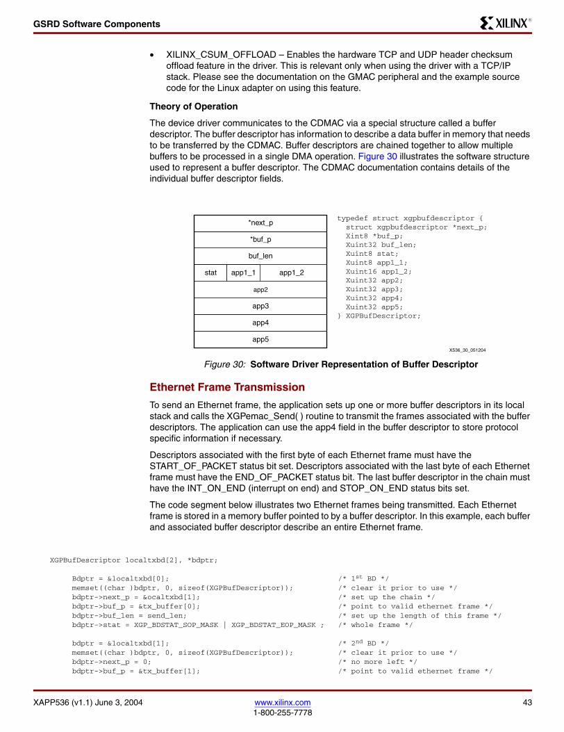
GSRD Software Components
XAPP536 (v1.1) June 3, 2004 www.xilinx.com 431-800-255-7778
R
• XILINX_CSUM_OFFLOAD – Enables the hardware TCP and UDP header checksum offload feature in the driver. This is relevant only when using the driver with a TCP/IP stack. Please see the documentation on the GMAC peripheral and the example source code for the Linux adapter on using this feature.
Theory of Operation
The device driver communicates to the CDMAC via a special structure called a buffer descriptor. The buffer descriptor has information to describe a data buffer in memory that needs to be transferred by the CDMAC. Buffer descriptors are chained together to allow multiple buffers to be processed in a single DMA operation. Figure 30 illustrates the software structure used to represent a buffer descriptor. The CDMAC documentation contains details of the individual buffer descriptor fields.
Ethernet Frame Transmission
To send an Ethernet frame, the application sets up one or more buffer descriptors in its local stack and calls the XGPemac_Send( ) routine to transmit the frames associated with the buffer descriptors. The application can use the app4 field in the buffer descriptor to store protocol specific information if necessary.
Descriptors associated with the first byte of each Ethernet frame must have the START_OF_PACKET status bit set. Descriptors associated with the last byte of each Ethernet frame must have the END_OF_PACKET status bit. The last buffer descriptor in the chain must have the INT_ON_END (interrupt on end) and STOP_ON_END status bits set.
The code segment below illustrates two Ethernet frames being transmitted. Each Ethernet frame is stored in a memory buffer pointed to by a buffer descriptor. In this example, each buffer and associated buffer descriptor describe an entire Ethernet frame.
XGPBufDescriptor localtxbd[2], *bdptr; Bdptr = &localtxbd[0]; /* 1st BD */ memset((char )bdptr, 0, sizeof(XGPBufDescriptor)); /* clear it prior to use */ bdptr->next_p = &ocaltxbd[1]; /* set up the chain */ bdptr->buf_p = &tx_buffer[0]; /* point to valid ethernet frame */ bdptr->buf_len = send_len; /* set up the length of this frame */ bdptr->stat = XGP_BDSTAT_SOP_MASK | XGP_BDSTAT_EOP_MASK ; /* whole frame */
bdptr = &localtxbd[1]; /* 2nd BD */ memset((char )bdptr, 0, sizeof(XGPBufDescriptor)); /* clear it prior to use */ bdptr->next_p = 0; /* no more left */ bdptr->buf_p = &tx_buffer[1]; /* point to valid ethernet frame */
Figure 30: Software Driver Representation of Buffer Descriptor
X536_30_051204
app3
app2
app1_2
app4
buf_len
*buf_p
*next_p
stat app1_1
app5
typedef struct xgpbufdescriptor { struct xgpbufdescriptor *next_p; Xint8 *buf_p; Xuint32 buf_len; Xuint8 stat; Xuint8 app1_1; Xuint16 app1_2; Xuint32 app2; Xuint32 app3; Xuint32 app4; Xuint32 app5;} XGPBufDescriptor;

44 www.xilinx.com XAPP536 (v1.1) June 3, 20041-800-255-7778
GSRD Software ComponentsR
bdptr->buf_len = send_len; /* set up the length of this frame */ bdptr->stat = XGP_BDSTAT_SOP_MASK | XGP_BDSTAT_EOP_MASK | XGP_BDSTAT_INT_ON_END_MASK | XGP_BDSTAT_STOP_ON_END_MASK ; /* whole frame - int and stop on last*/
XGPemac_SgSend(&instance, &localtxbd[0], 0); /* send out frame */
The software driver maintains a transmit queue of buffer descriptors that are waiting to be transmitted. This transmit queue is useful in the case where the DMA transmit engine is busy executing a prior transaction. The driver waits until the DMA transmit engine is idle before the queue is given to the engine.
The XGPemac_SgSend( ) in the example above copies over information from the local buffer descriptors into two buffer descriptors in the internal chain of buffer descriptors. This approach enforces the fact that the Ethernet frames can never be sent out of order. The driver then inserts these descriptors into the transmit queue and initiates a DMA transmit transaction when the engine is idle (not busy).
When the frames are transmitted successfully, an interrupt is generated because the application set the interrupt flag in the last buffer descriptor of the chain. The software driver services the interrupt. The DMA engine marks all the buffer descriptors that it processed by setting the COMPLETED bit in the status field of the descriptor. The software driver interrupt handler “scrubs” the buffer descriptor by clearing the COMPLETE bit so they can be re-used for future transmissions.
The driver interrupt handler then calls the application callback function previously registered with the XGPemac_SetSgSendHandler( ) function. The number of frames successfully transmitted and the actual chain of buffer descriptors that were processed (transmitted) are passed to the callback function. The callback function performs any application-related housekeeping functions (for example, freeing any protocol-related structures that it stored in the app4 field of the buffer descriptor). The callback function is executed in the context of the interrupt handler and all interrupts are typically disabled, so it needs to be as short as possible.

GSRD Software Components
XAPP536 (v1.1) June 3, 2004 www.xilinx.com 451-800-255-7778
R
Figure 31 is a visual representation of the data structures used to manage the internal chain of Transmit buffer descriptors. There are separate XGPDmaEngine structures for managing the Transmit and for the Receive DMA engines. Both structures are contained in the main XGPemac structure. Each XGPDmaEngine structure contains a XGPQueue structure to help implement a queue (currently implemented for the transmit side only).
The relevant fields in the XGPDmaEngine structure are listed below:
• Head points to the start of the chain of buffer descriptors (in this example, buffer descriptor 0).
• Scrub points to the next buffer descriptor in the chain that needs to be serviced by the interrupt handler (in this example, buffer descriptor 2).
• Free points to the next free buffer descriptor available for transmit (in this example, buffer descriptor 7).
The relevant fields in the XGPQueue structure are listed below:
• Qhead points to the start of the transmit queue of buffer descriptors that needs to be processed by the DMA engine (buffer descriptor 4 in this example).
• Qtail points to the last buffer descriptor in the transmit queue of buffer descriptors (in this example, buffer descriptor 5).
• Qlen points to the current length of the transmit queue (in this example, 2).
In the example shown in Figure 31, the DMA engine is currently working on buffer descriptor 3. Descriptors 4 and 5 are in the transmit queue waiting to be processed. Descriptor 6 has been requested by the application but has not yet been inserted into the transmit queue. Descriptors 7, 0 and 1 are available for use, and descriptor 2 has been processed and the interrupt handler has not yet scrubbed it.
Figure 31: Data Structures Used to Manage Chain of Transmit Buffer Descriptor Chain
X536_31_051204
6
7
5
4
2
3
1
0
Qhead
Qtail
Qlen
Head
Scrub
Free
XGPQueue XGPDmaEngine

46 www.xilinx.com XAPP536 (v1.1) June 3, 20041-800-255-7778
GSRD Software ComponentsR
Ethernet Frame Reception
The chain of receive buffer descriptors must be set up and initialized with valid receive buffers prior to calling the XGPemac_SgRecv( ) function. This function must be called only once by the application during initialization. The DMA engine independently operates on the chain of receive buffer descriptors after that point.
The DMA receive engine transfers Ethernet frames from the GMAC Peripheral Receive FIFO and places them into the memory location pointed to by the first free receive buffer descriptor. After transferring the frame to memory, the DMA engine marks the COMPLETE, START_OF_PACKET, and END_OF_FRAME bits in the status field of the buffer descriptor. If the INT_ON_END status bit is set in the buffer descriptor, the CDMAC also generates an interrupt. The software device driver interrupt handler “scrubs” the processed descriptor(s) by clearing the COMPLTE, START_OF_PACKET, and END_OF_PACKET bits in the status field of the buffer descriptor(s). It then calls the application callback function with the number of frames successfully received. The application callback function must be as short as possible because it is executed in the context of the interrupt handler when all interrupts are typically disabled. The callback function must process the received buffers and refill the buffer descriptors with empty receive buffers.
Note: Any application related fields in the buffer descriptor cannot be used on the receive side for storing protocol related information (unlike the transmit side where this is possible.
The device driver does not need to queue receive buffer descriptors. The XGPqueue structure is not used for the receive side. The head and scrub data structures in the XGPDmaEngine structure are used to manage the circular chain of receive buffer descriptors.
In the example shown in Figure 32, the head variable in the XGPDmaEngine structure points to the head of the chain of receive descriptors. The scrub variable is the next descriptor that needs to be scrubbed by the interrupt handler.
Figure 32: Data Structures Used to Manage Chain of Receive Buffer Descriptors
X536_32_051204
6
7
5
4
2
3
1
0
Head
Scrub
Free
XGPDmaEngine
GSRD Software Components
XAPP536 (v1.1) June 3, 2004 www.xilinx.com 471-800-255-7778
R
Note: The last descriptor in the chain (in this example, buffer descriptor 7) must have the STOP_ON_END status bit set. This allows the processing of received data to catch up with data received at a high rate on the Ethernet network, since the DMA engine stops after transferring data into the buffer pointed to by buffer descriptor 7. The device driver automatically restarts the DMA engine when it is idle.
Interrupt Moderation (Coalescing)
Without Interrupt Moderation, every frame received or transmitted generates an interrupt and the interrupt handler scrubs the buffer descriptor while servicing the interrupt. For high data rates, this can lead to a large number of interrupts to the CPU, which reduces the throughput of the Ethernet link. The Interrupt Moderation (coalescing) feature mitigates this problem by interrupting the CPU only when a certain number of Ethernet frames has been received. This value can be tuned for optimum performance. If it is too low, the CPU is interrupted too often and if the value is too high, the CPU spends more time in the interrupt handler since it has to scrub more descriptors per interrupt.
On the transmit side, the device driver code enforces the coalescing threshold value while inserting the buffer descriptors in the transmit queue. It ensures the INT_ON_END status bit is set after every N descriptors, where N is the coalescing threshold value for the transmit side. The driver also ensures the last descriptor to be transmitted has the INT_ON_END and STOP_ON_END bits set. This ensures that an interrupt is generated after all the frames have been transmitted and the CDMAC stops.
On the receive side, the coalescing of interrupts causes the need to set up a periodic timer to poll the receive buffers for data. The reason for this can be explained with an example. If the receive interrupt coalescing value is 10 and the Ethernet channel receives five frames before the channel goes idle (no more received frames), the five frames will never be processed by the CPU since it never received an interrupt. This can lead to higher protocol errors like TCP connection timeouts etc. Even for a channel with constant traffic, this can lead to higher latencies and lower throughput. The CDMAC contains a programmable timer that can be used to generate an interrupt every ~100 uS if the coalescing threshold has not been met.
Software File List
The files that make up the software drivers are listed below:
GMAC Peripheral driver files:
Xgpemac.c – main source file
Xgpemac.h – main header file
Xgpemac_l.h – low-level driver definitions
Xgpemac_g.c – peripheral configuration file
CDMAC driver files:
Xgpdma.c – main CDMAC source file
Xgpdma.h – main CDMAC header file
Xgpdma_l.h – CDMAC driver low-level driver definitions
Xgpconf.h – general software driver configuration file
Device Driver Software API
The xapp536.zip file contains API Documentation for the Device Driver in HTML format. Open the gsrd/doc/drivers/ gsrdxgpemac_dma_v1_00_b/index.html with your favorite web browser. This documentation was generated directly from the source code using an open source tool Doxygen. More information about Doxygen can be found here: http://www.doxygen.org/.

48 www.xilinx.com XAPP536 (v1.1) June 3, 20041-800-255-7778
GSRD Software ComponentsR
Bare Metal Ethernet Transmit and Receive Tests
The following applications are designed to test and demonstrate the functionality of the GSRD EDK Reference System. These tests are implemented with stand-alone software running on the embedded PowerPC 405.
The stand-alone test is based on the gsrd_gmac_example stand-alone application available in the reference design ZIP file (under the gsrd/sw/standalone/gsrd_gmac_example/ directory). A Spirent SmartBits performance analysis system is connected to the GSRD Reference System on the ML300 board. The interrupt coalescing value on the receive is set to 10 (every 10 frames generate an interrupt), and there are 100 Tx and 100 Rx buffer descriptors in the test.
The transmit numbers are obtained from statistics obtained on the SmartBits system. A pre-allocated buffer is sent continuously in a loop using a chain of buffer descriptors. The receive numbers are obtained by setting up the Programmable Interrupt Timer (PIT) to generate an interrupt every second to the PowerPC on the GSRD Reference System. The total number of valid Ethernet frames received per second is printed to the console.
Table 8 and Table 9 show the raw Ethernet performance numbers for various frame sizes. The “Line Performance” column is calculated by multiplying the raw “Frame Size” by the “Frames per Second.” The “Payload Performance” column is calculated by multiplying the payload portion of the “Frame Size.”
Table 8: Bare Metal Ethernet Transmit Performance
Frame Size (including FCS)
Frames per Second
Line Performance
(Mbps)
Payload Performance
(Mbps)
64 575,428 294.62 211.76
128 597,472 611.81 525.78
512 233,012 954.42 920.86
1518 80,656 979.49 967.87
5000 24,736 989.44 985.88
9000 13,775 991.80 989.82
Table 9: Bare Metal Ethernet Receive Performance
Frame Size (including FCS)
Frames per Sec-ond
Line Performance (Mbps)
Payload Perfor-mance(Mbps)
64 779,800 399.26 286.97128 560,120 573.56 492.91512 235,000 962.56 928.721518 81,300 987.31 975.605000 24,900 996.00 992.419000 13,057 940.10 938.22

GSRD Software Components
XAPP536 (v1.1) June 3, 2004 www.xilinx.com 491-800-255-7778
R
Linux on GSRD Reference System
Linux has been ported to the GSRD EDK Reference System on ML300. Linux boots from a RAM Disk image embedded in the supplied ELF file. More information about this can be found in the readme_linux.txt file located in the gsrd/sw/os/linux/ directory of the ZIP file.
Netperf is an open source benchmark utility that measures networking performance. It was used to measure the TCP performance of Linux on GSRD. Table 10 and Table 11 summarize the Netperf benchmark results of Linux on GSRD running on the ML300 platform. The raw output from the Netperf utility is captured in the file performance_linux.txt in the gsrd/sw/os/linux/ directory.
Linux supports a special system call for transmitting TCP data, sendfile(). The system call sendfile() enables zero-copy transmission of data, which allows Linux to also take advantage of the checksum (CSUM) offload capabilities of the GMAC Peripheral. Netperf can be run with the sendfile() system call.
Table 10: Netperf Transmit Benchmark Results
Frame SizeReceive
Socket Size(bytes)
Send Socket Size
(bytes)
Send Message Size
(bytes)
sendfile() with CSUM
Offload
CPU Utilization
Bandwidth(Mbps)
128 87380 16384 16384 NO 100% 8
128 87380 16384 16384 YES 99% 8
512 87380 16384 16384 NO 99% 47
512 87380 16384 16384 YES 98% 47
1518 87380 16384 16384 NO 98% 112
1518 87380 16384 16384 YES 97% 121
5000 87380 16384 16384 NO 97% 204
5000 87380 16384 16384 YES 97% 296
9000 87380 16384 16384 NO 96% 272
9000 87380 16384 16384 YES 96% 546
Table 11: Netperf Receive Benchmark Results
Frame SizeReceive
Socket Size(bytes)
Send Socket Size
(bytes)
Send Message Size
(bytes)
sendfile() with CSUM
Offload
CPU Utilization
Bandwidth(Mbps)
128 87380 16384 16384 NO 100% 26
512 87380 16384 16384 NO 99% 44
1518 87380 16384 16384 NO 94% 115
5000 87380 16384 16384 NO 95% 241
9000 87380 16384 16384 NO 96% 264

50 www.xilinx.com XAPP536 (v1.1) June 3, 20041-800-255-7778
Building the GSRD Reference System under EDKR
There is no equivalent system call for zero-copy reception of TCP data in Linux – there is still a single copy in this system from Kernel to User space. For this reason, the checksum offload capability of the GMAC Peripheral is not used on the receive side under Linux.
For more information about sendfile() on Linux, see:
http://builder.com.com/5100-6372-1044112.html.
For more information about Netperf, see the Netperf website:
http://www.netperf.org/.
Stand-alone TCP/IP Stack
Stand-alone TCP/IP can be used with GSRD when the highest performance possible is required. The overhead of running a full operating system like Linux is noticeable when communicating on a Gigabit Ethernet network. lwIP is an open source TCP/IP implementation for small embedded systems where no operating system is required, although it can be used with an operating system. lwIP is discussed in XAPP663. Work is currently ongoing to port a stand-alone TCP/IP Stack to GSRD. As of the date of this publication, this work had not been completed and will be released in a future version of GSRD.
Building the GSRD Reference System under EDK
The gsrd/doc/EDK_instructions.pdf document included with the reference design contains instructions for building the GSRD Reference System under EDK. The section below describes the special considerations for the 1-Gigabit Ethernet MAC LogiCORE.
Xilinx 1-Gigabit Ethernet MAC LogiCORE Integration
The GSRD EDK Reference System is shipped with an evaluation simulation model of the 1-Gigabit Ethernet MAC. This model (gsrd/edk_libs/gsrd_lib/pcores/ll_gmac_periph_v1_00_a/hdl/verilog/gmac.v) can be used for behavioral simulation only. To generate a bit file through EDK, a “Full System Hardware Evaluation” license of the 1-Gigabit Ethernet MAC must be obtained from Xilinx. Follow the instructions on this web page to obtain the license and necessary ISE updates.
The COREGen tool is used to generate the netlist for the 1-Gigabit Ethernet MAC LogiCORE. Be sure to configure the core as shown in Figure 33. After the core is generated, copy the resulting gmac.edn and gmac_gmac_gen_1.ngc files into the gsrd/edk_libs/gsrd_lib/pcores/ll_gmac_periph_v1_00_a/netlist/ directory. The gmac.v in the gsrd/edk_libs/gsrd_lib/pcores/ll_gmac_periph_v1_00_a/hdl/verilog/ directory can still be used as the black-box wrapper and simulation model as long as the configuration options are kept the same as shown in Figure 33.

Reference Design Files
XAPP536 (v1.1) June 3, 2004 www.xilinx.com 511-800-255-7778
R
Reference Design Files
Xilinx ML300 Evaluation Platform
LocalLink Specification
1-Gigabit Ethernet MAC Data Sheet
XAPP535 High Performance Multi Port Memory Controller
The reference design can be downloaded from the Xilinx website: xapp536.zip.
Getting Started with EDK and MontaVista Linux
Revision History
The following table shows the revision history for this document.
Figure 33: Gigabit Ethernet MAC COREGen Configuration Screen Capture
Date Version Revision
05/05/04 1.0 Initial Xilinx release.
06/03/04 1.1 Added introductory summary, updated graphics, and general content edit.