xilinx ds617 platform flash xl high-density configuration ... · • standard nor-flash interface...
TRANSCRIPT

DS617 (v2.2) October 29, 2008 www.xilinx.comPreliminary Product Specification 1
© 2007–2008 Xilinx, Inc. XILINX, the Xilinx logo, Virtex, Spartan, ISE, and other designated brands included herein are trademarks of Xilinx in the United States and other countries. PCI, PCIe and PCI Express are trademarks of PCI-SIG and used under license. All other trademarks are the property of their respective owners.
Features• In-System Programmable Flash Memory Optimized for
Virtex®-5 FPGA Configuration
• High-Performance FPGA Bitstream Transfer up to 800 Mb/s (50 MHz(1) × 16-bits), Ideal for Virtex-5 FPGA PCI Express® Endpoint Applications
• MultiBoot Bitstream, Design Revision Storage
• FPGA Configuration Synchronization (READY_WAIT) Handshake Signal
• ISE® Software Support for In-System Programming via Xilinx® JTAG Cables(2)
• Standard NOR-Flash Interface for Access to Code or Data Storage
• Operation over Full Industrial Temperature Range (–40°C to +85°C)
• Common Flash Interface (CFI)
• Low-Power Advanced CMOS NOR-Flash Process
• Endurance of 10,000 Program/Erase Cycles Per Block
• Power Supplies
♦ Industry-Standard Core Power Supply Voltage (VDD) = 1.8V
♦ 3.3V, 2.5V, or 1.8V I/O (VDDQ) Power Supply Voltage
• Memory Organization
♦ 128-Mb Main Array Capacity
♦ 16-bit Data Bus
♦ Multiple 8-Mb Bank Architecture for Dual Erase/Program and Read Operation
♦ 127 Regular 1-Mb Main Blocks
♦ 4 Small 256-Kb Parameter Blocks
• Synchronous/Asynchronous Read Modes
♦ Power-On in Synchronous Burst Read Mode at up to 54 MHz
♦ Asynchronous Random Access Time = 85 ns
♦ Accelerated Asynchronous Page Read Mode
• Protection
♦ Default Block Protection at Power-Up
♦ Hardware Write Protection (when VPP = VSS)
• Security
♦ Unique Device Number (64-bits)
♦ One-Time-Programmable (OTP) Registers
• Small-Footprint (10 mm × 13 mm) FT64 Packaging
DescriptionA reliable compact high-performance configuration bitstream storage and delivery solution is essential for the high-density Virtex-5 FPGAs. Platform Flash XL is the industry's highest performing configuration and storage device and is specially optimized for high-performance Virtex-5 FPGA configuration and ease-of-use. Platform Flash XL integrates 128 Mb of in-system programmable flash storage and performance features for configuration within a small-footprint FT64 package (Figure 5). Power-on burst read mode and dedicated I/O power supply enable Platform Flash XL to mate seamlessly with the native SelectMap configuration interface of Virtex-5 FPGAs. A
wide, 16-bit data bus delivers the FPGA configuration bitstream at speeds up to 800 Mb/s without wait states.
Platform Flash XL is a non-volatile flash storage solution, optimized for FPGA configuration. The device provides a READY_WAIT signal that synchronizes the start of the FPGA configuration process, improving both system reliability and simplifying board design. Platform Flash XL can download an XC5VLX330 bitstream (79,704,832 bits) in less than 100 ms, making the configuration performance of Platform Flash XL ideal for Virtex-5 FPGA Endpoint solutions for PCI Express and other high-performance applications.
90 Platform Flash XL High-Density Configuration
and Storage Device
DS617 (v2.2) October 29, 2008 Preliminary Product Specification
R
1. System considerations can lower the configuration clock frequency below the maximum clock frequency for the device. To determine the maximum configuration clock frequency, check the minimum clock period (TKHKH) for the chosen I/O voltage range (VDDQ), the clock High-to-output valid time (TKHQV), and the FPGA SelectMAP setup time.
2. ISE software supports indirect, in-system programming via specific configurations of Virtex-5 FPGAs and Platform Flash XL devices (see "iMPACT Programming Solution for Prototype FPGA Designs," page 12).
www.BDTIC.com/XILINX

Platform Flash XL High-Density Configuration and Storage Device
DS617 (v2.2) October 29, 2008 www.xilinx.comPreliminary Product Specification 2
R
Platform Flash XL is a single-chip configuration solution with additional system-level capabilities. A standard NOR flash interface (Figure 2) and support for common flash interface (CFI) queries provide industry-standard access to the device memory space. The Platform Flash XL's 128 Mb capacity can typically hold one or more FPGA bitstreams. Any memory space not used for bitstream storage can be used to hold general purpose data or embedded processor code.
Platform Flash XL integrates well with the Xilinx design and debug tool suite for Virtex-5 FPGAs. The ISE software supports indirect, in-system programming of Platform Flash XL via the single IEEE Standard 1149.1 (JTAG) port on the Virtex-5 FPGA for prototype programming (Figure 3).
X-Ref Target - Figure 1
Notes: 1. System considerations can lower the configuration clock frequency below the maximum clock frequency for the device. To determine the
maximum configuration clock frequency, check the minimum clock period (TKHKH) for the chosen I/O voltage range (VDDQ), the clock High-to-output valid time (TKHQV), and the FPGA SelectMAP setup time.
Figure 1: Platform Flash XL Delivers Reliable, High-Performance FPGA Configuration
ConfigurationSynchronization
Handshake
Clock up to 50 MHz(1)
Wide (16-bit) Data Path
Virtex-5 FPGA
Sel
ectM
AP
Por
t
Platform Flash XL
READY_WAIT
FPGA Design(.bit) File
DS617_01_100308
Up to 800 Mb/s
X-Ref Target - Figure 2
Figure 2: Standard NOR Flash Interface for User Access to Memory
Platform Flash XL
User Design
Virtex-5 FPGA
Control
Address
Data/Commands
Code
User Data
Design (.bit)File, Rev. 1
Design (.bit)File, Rev. 0
DS617_02_032508
X-Ref Target - Figure 3
Figure 3: Indirect Programming Solution for Platform Flash XL
Xilinx JTAGCable Connector
Platform Flash XL
Sta
ndar
d N
OR
Fla
sh In
terf
ace
FPGA Design(.bit) File
Virtex-5 FPGA
For ProgrammingPlatform Flash XL
IEE
E 1
149.
1(J
TAG
) P
ort
BP
I Fla
shC
onfig
urat
ion
Por
t
Indirect,In-System
ProgrammingEngine
For ProgrammingPlatform Flash XL
Control
Address
Data/Commands
Single Cable Connector forDirect FPGA Configuration/Debug and
Indirect Platform Flash XLProgramming
DS617_03_050108
www.BDTIC.com/XILINX

Platform Flash XL High-Density Configuration and Storage Device
DS617 (v2.2) October 29, 2008 www.xilinx.comPreliminary Product Specification 3
R
Flash Memory Architecture OverviewPlatform Flash XL is a 128-Mb (8 Mb × 16) non-volatile flash memory. The device is in-system programmable with a 1.8V core (VDD) power supply. A separate I/O (VDDQ) power supply enables I/O operation at 3.3V, 2.5V, or 1.8V. An optional 9V VPP power supply can accelerate factory programming.
A common flash interface (CFI) provides access to device memory (Figure 3, page 2). Moreover, Platform Flash XL supports multiple read modes. A 23-bit address bus provides random read access to each 16-bit word. Four words occupy each page for accelerated page mode reads. The device powers-up in a synchronous burst read mode capable of sequential read rates up to 54 MHz.
Platform Flash XL has a multiple-bank architecture. An array of 131 individually erasable blocks are divided into 16, 8-Mb banks. Fifteen main banks contain uniform blocks of 64 Kwords, and one parameter bank contains seven main blocks of 64 Kwords, plus four parameter blocks of 16 Kwords.
Note: The device is electronically erasable at the block level and programmable on a word-by-word basis.
The multiple-bank architecture allows dual operations — read operations can occur on one bank while a program or erase operation occurs in a different bank. However, only one bank at a time is allowed to be in program or erase mode. Burst reads are allowed to cross bank boundaries.
Table 1 summarizes the bank architecture, and the memory map is shown in Figure 4, page 4. The parameter blocks are located at the top of the memory address space in Platform Flash XL.
Each block can be erased separately. Erase operations can be suspended in order to perform a program or read operation in any other block and then resumed. Program operations can
be suspended to read data at any memory location except for the one being programmed, and then resumed.
Program and erase commands are written to the command interface of the memory. An internal program/erase controller takes care of the timing necessary for program and erase operations. The end of a program or erase operation can be detected and any error conditions identified in the status register. The command set required to control the memory is consistent with JEDEC standards.
The device supports synchronous burst read and asynchronous read from all blocks of the memory array. At power-up, the device is configured for synchronous read. In synchronous burst read mode, data is output on each clock cycle at frequencies of up to 54 MHz. The synchronous burst read operation can be suspended and resumed.
When the bus is inactive during asynchronous read operations, the device automatically switches to an automatic standby mode. In this condition the power consumption is reduced to the standby value, and the outputs are still driven.
Platform Flash XL features an instant, individual block-locking scheme, allowing any block to be locked or unlocked with no latency, and enabling instant code and data protection. All blocks have three levels of protection. Blocks can be locked and locked-down individually preventing any accidental programming or erasure. There is an additional hardware protection against program and erase: when VPP = VPPLK all blocks are protected against program or erase. All blocks are locked at power-up.
The device features a separate region of 17 programmable registers whose values can be protected against further programming changes. Sixteen of these registers are each 128-bits in size, with the 17th register subdivided into two 64-bit registers. One of the 64-bit registers contains a factory preprogrammed, unique device number, permanently protected against modification. The second 64-bit register is user-programmable.
All bits within these registers (except for the permanently-protected unique number register) are one-time-programmable (OTP) — each bit can be programmed only once from a one-value to a zero-value.
Two protection lock registers can be programmed to lock any of the 17 protectable registers against further changes. One protection lock register contains bits that determine the protection state of the two special 64-bit registers. The bit corresponding to the unique device number register is pre-programmed to ensure the unique device number register is permanently protected against modification. The second protection lock register contains OTP bits that correspond the protection state each of the remaining 16 registers.
Platform Flash XL is available in a 10 × 13 mm, 1.0 mm-pitch FT64 package and supplied with all the bits erased (set to '1').
Table 1: Bank Architecture
Number Bank Size Parameter Blocks Main Blocks
Parameter Bank 8 Mbits 4 blocks of
16 Kwords7 blocks of 64 Kwords
Bank 1 8 Mbits – 8 blocks of 64 Kwords
Bank 2 8 Mbits – 8 blocks of 64 Kwords
Bank 3 8 Mbits – 8 blocks of 64 Kwords
… … … …
Bank 14 8 Mbits – 8 blocks of 64 Kwords
Bank 15 8 Mbits – 8 blocks of 64 Kwords
www.BDTIC.com/XILINX

Platform Flash XL High-Density Configuration and Storage Device
DS617 (v2.2) October 29, 2008 www.xilinx.comPreliminary Product Specification 4
R
X-Ref Target - Figure 4
Figure 4: Platform Flash XL Memory Map(Address Lines A22 – A0)
64 Kword
64 Kword
64 Kword
64 Kword
64 Kword
64 Kword
64 Kword
64 Kword
64 Kword
64 Kword
16 Kword
16 Kword
000000h
00FFFFh
070000h
07FFFFh
600000h
60FFFFh
670000h
67FFFFh
680000h
68FFFFh
6F0000h
6FFFFFh
700000h
70FFFFh
770000h
77FFFFh
78FFFFh
780000h
7E0000h
7EFFFFh
7F0000h
7F3FFFh
7FC000h
7FFFFFh
Bank 15
Bank 3
Bank 2
Bank 1
ParameterBank
8 MainBlocks
8 MainBlocks
8 MainBlocks
8 MainBlocks
7 MainBlocks
4 ParameterBlocks
DS167_04_053008
Address
www.BDTIC.com/XILINX

Platform Flash XL High-Density Configuration and Storage Device
DS617 (v2.2) October 29, 2008 www.xilinx.comPreliminary Product Specification 5
R
Pinout and Signal DescriptionsSee Figure 5 and Table 2 for a logic diagram and brief overview of the signals connected to this device.
Address Inputs (A22-A0)
The Address inputs select the words in the memory array to access during Bus Read operations. During Bus Write operations they control the commands sent to the Command Interface of the Program/Erase Controller.
Data Inputs/Outputs (DQ15-DQ0)
The Data I/O output the data stored at the selected address during a Bus Read operation or input a command or the data to be programmed during a Bus Write operation.
Chip Enable (E)
The Chip Enable input activates the memory control logic, input buffers, decoders and sense amplifiers. When Chip Enable is at VIL and Reset is at VIH, the device is in active mode. When Chip Enable is at VIH, the memory is
deselected, the outputs are high impedance, and the power consumption is reduced to the standby level.
Output Enable (G)
The Output Enable input controls data outputs during the Bus Read operation of the memory. Before the start of the first address latching sequence (FALS), the Output Enable input must be held Low before the clock starts toggling.
Write Enable (W)
The Write Enable input controls the Bus Write operation of the memory’s Command Interface. The data and address inputs are latched on the rising edge of Chip Enable or Write Enable, whichever occurs first.
Table 2: Signal Names
Signal Name Function Direction
A22-A0 Address Inputs Inputs
DQ15-DQ0 Data Input/Outputs, Command Inputs I/O
E Chip Enable Input
G Output Enable Input
W Write Enable Input
RP Reset Input
WP Write Protect Input
K Clock Input
L Latch Enable Input
READY_WAIT Ready/Wait I/O
VDD Supply Voltage –
VDDQSupply Voltage for
Input/Output Buffers –
VPP
Optional(1) Supply Voltage for Fast
Program and Erase –
VSS Ground –
VSSQGround Input/output
Supply –
NC Not Connected Internally –
Notes: 1. Typically, VPP is tied to the VDDQ supply on a board. See the VPP
Program Supply Voltage section for alternate options.
X-Ref Target - Figure 5
Figure 5: Logic Diagram
PlatformFlash XL
READY_WAIT
A22–A0
W
K
VSS VSSQ
VDD VDDQ VPP
DQ15–DQ0
16
E
G
RP
WP
L
DS617_05_053008
23
www.BDTIC.com/XILINX

Platform Flash XL High-Density Configuration and Storage Device
DS617 (v2.2) October 29, 2008 www.xilinx.comPreliminary Product Specification 6
R
Write Protect (WP)Write Protect is an input that gives an additional hardware protection for each block. When Write Protect is at VIL, the Lock-Down is enabled, and the protection status of the Locked-Down blocks cannot be changed. When Write Protect is at VIH, the Lock-Down is disabled, and the Locked-Down blocks can be locked or unlocked.
Reset (RP)The Reset input provides a hardware reset of the memory. When Reset is at VIL, the memory is in reset mode: the outputs are high impedance, and the current consumption is reduced to the Reset supply current IDD2. After Reset all blocks are in the Locked state, and the Configuration Register is reset. When Reset is at VIH, the device is in normal operation. Exiting reset mode the device enters the synchronous read mode and the FALS is executed.
X-Ref Target - Figure 6
Notes: 1. See the FT64/FTG64 package specifications at http://www.xilinx.com/support/documentation/package_specifications.htm.
Figure 6: FT64 Package Connections (Top View through Package)
DQ6
A0
VSSQVDD
DQ10
VDD
DQ7
DQ5VDDQDQ2
H
DQ14
VSSDQ13
D A15
A19
EA8
C
A16
A20
A10
A14
K
A7
B A18A1
A12
A13
A
87654321
A6A2
A3 A4
G
F
E
DQ0
A5 VPP A17
A9 A11
RP
DQ15DQ9DQ8 DQ1 DQ4DQ3
GDQ12DQ11
W
VSS NC
NC
NC NC
NC
NC
NC NC
NC
A21
A22
READY_WAIT
WP
NC
L
DS617_10_110807
www.BDTIC.com/XILINX

Platform Flash XL High-Density Configuration and Storage Device
DS617 (v2.2) October 29, 2008 www.xilinx.comPreliminary Product Specification 7
R
Latch Enable (L)
Latch Enable latches the address bits on its rising edge. The address latch is transparent when Latch Enable is at VIL and inhibited when Latch Enable is at VIH.
The Latch Enable (L) signal must be held at VIH during the power-up phase, during the FALS restart phase and through the entire FALS.
In asynchronous mode, the address is latched on L going High. or addresses are sent continuously if L is held Low. During Write operations, L can be tied Low (VIL) to allow the addresses to flow through.
Clock (K)
The Clock input synchronizes the memory to the FPGA during synchronous read operations. The address is latched on a Clock edge (rising or falling, according to the configuration settings) when Latch Enable is at VIL. Clock is ignored during asynchronous read and in write operations.
Ready/Wait (READY_WAIT)Caution! The READY_WAIT requires an external pull-up resistor to VDDQ. The external pull-up resistor must be sufficiently strong to ensure a clean, Low-to-High transition within less than one microsecond (TRWRT) when the READY_WAIT pin is released to a high-impedance state.
READY_WAIT can perform one of two functions. By default, READY_WAIT is an input/open-drain ready signal coordinating the initiation of the device's synchronous read operation with the start of an FPGA configuration sequence. Optionally, READY_WAIT can be dynamically configured as an output wait signal, indicating a wait condition during a synchronous read operation.
Upon a power-on reset (POR) or RP-pin reset event, the device drives READY_WAIT to VIL until the device is ready to initiate a synchronous read or receive a command. When the device reaches an internal ready state from a reset condition, READY_WAIT is released to a high-impedance state (an external pull-up resistor to VDDQ is required to externally pull the READY_WAIT signal to a valid input High). The device waits until the READY_WAIT input becomes a valid input High before permitting a synchronous read or accepting a command. Connecting the READY_WAIT to the FPGA
INIT_B pin in a wired-and circuit creates a handshake coordinating the initiation of the device synchronous read with the start of the FPGA configuration sequence.
When READY_WAIT is an input/open-drain ready signal, the system can drive READY_WAIT to VIL to reinitiate a synchronous read operation. A valid address must be provided to the device for a reinitiated synchronous read operation.
Optionally, READY_WAIT can be configured as an output signaling a wait condition during a synchronous read operation. The wait condition indicates a clock cycle during which the output data is not valid. When configured as an output wait signal, READY_WAIT is high impedance when Chip Enable is at VIH or Output Enable is at VIH. Only when configured as a wait signal, READY_WAIT can be configured to be active during the wait cycle or one clock cycle in advance, and the READY_WAIT polarity can be configured.
VDD Supply VoltageVDD provides the power supply to the internal core of the memory device and is the main power supply for all operations (Read, Program and Erase).
VDDQ Supply VoltageVDDQ provides the power supply to the I/O pins and enables all outputs to be powered independently of VDD.
VPP Program Supply VoltageVPP is either a control input or a power supply pin, selected by the voltage range applied to the pin.
If VPP is kept in a low voltage range (0V to VDDQ), VPP is seen as a control input. In this case a voltage lower than VPPLK gives absolute protection against program or erase, while VPP in the VPP1 range enables these functions. VPP is only sampled at the beginning of a program or erase — a change in its value after the operation starts does not have any effect, and all program or erase operations continue.
If VPP is in the range of VPPH, the signal acts as a power supply pin. In this condition VPP must be stable until the Program/Erase algorithm is completed.
VSS GroundVSS Ground is the reference for the core supply and must be connected to the system ground.
VSSQ GroundVSSQ Ground is the reference for the input/output circuitry driven by VDDQ. VSSQ must be connected to VSS.
Note: Each device in a system should have VDD, VDDQ and VPP decoupled with a 0.1 μF ceramic capacitor close to the pin (high-frequency, inherently low-inductance capacitors should be placed as close as possible to the package). The PCB track widths should be sufficient to carry the required VPP program and erase currents.
Table 3: Latch Enable Logic Levels in Synchronous and Asynchronous Modes
Operation Asynchronous Synchronous
Bus Read X VIH
Bus Write X or toggling X or toggling
Address Latch Toggling Toggling
Standby X X
Reset VIH VIH
FALS VIH VIH
Power-up VIH VIH
www.BDTIC.com/XILINX

Platform Flash XL High-Density Configuration and Storage Device
DS617 (v2.2) October 29, 2008 www.xilinx.comPreliminary Product Specification 8
R
FPGA Configuration OverviewPlatform Flash XL enables the rich set of Virtex-5 FPGA configuration features without additional glue logic. The device delivers the FPGA bitstream at power-on through a 16-bit data bus at data rates up to 800 Mb/s. Virtex-5 FPGAs can also be configured from one of many design/revision bitstreams stored in the device. These revision bitstreams are accessed through the Virtex-5 family’s MultiBoot addressing and fallback features available in specific system configurations with Platform Flash XL. For detailed descriptions of the Virtex-5 FPGA configuration features and configuration procedure, see UG191, Virtex-5 FPGA Configuration User Guide.
At a high level, the general procedure for FPGA configuration from Platform Flash XL is as follows:
1. A system event, such as power-up, initiates the FPGA configuration process.
2. The FPGA and Platform Flash XL release their respective INIT_B and READY_WAIT pins, synchronizing the start of the configuration process.
3. The FPGA samples its mode pins to determine its configuration mode.
4. The device latches its starting address for its impending burst read operation.
5. Each 16-bit word of the bitstream is synchronously transferred from the device to the FPGA at each rising edge of the configuration clock.
6. The FPGA begins operation and asserts DONE to indicate the completion of the configuration procedure.
Platform Flash XL(1) can configure the Virtex-5 FPGA using either Master BPI-Up(2), Slave-SelectMAP, or Master-SelectMAP configuration modes (Slave-SelectMAP mode is recommended). See Table 4 for a summary of attributes for different configuration modes and memories.
1. Platform Flash XL does not support FPGA configuration in the following modes: JTAG, Master-Serial, Slave-Serial, Master-SPI, and Master-BPI-Down.
2. BPI-Up = Byte (or word) peripheral interface in which the flash read address counts upward during the configuration process. For details, see the Virtex-5 FPGA Configuration User Guide.
Table 4: Virtex-5 FPGA Configuration Mode Overview
Platform Flash XL Third-Party Standard BPI Flash
(85-ns Access Time)High-Performance
Configuration ModeStandard BPI Flash Compatibility Mode
FPGA Configuration Mode Slave-SelectMAP mode Master-BPI mode Master-BPI mode
Guaranteed Bitstream Transfer Bandwidth at Best Clock Setting
800 Mb/s(1) 248 Mb/s(2) 112 Mb/s(3)
Power Sequence Immunity Special precautions required(4) Special precautions required(4)
Multipurpose FPGA Pins Actively Used During Configuration(5)
17(6) 46 46
Xilinx Support For limited setups(7)
MultiBoot Capable
Notes: 1. External configuration clock source frequency = 50 MHz.2. Bandwidth considers Virtex-5 FPGA FMCCKTOL = ±50%. BitGen ConfigRate = 31.3. Bandwidth considers Virtex-5 FPGA FMCCKTOL = ±50%. BitGen ConfigRate = 21, bpi_page_size = 4, bpi_1st_read_cycle = 3. First word
access time = 85 ns; Page word access = 25 ns.4. The Platform Flash XL can only delay the start of the FPGA configuration process by holding its READY_WAIT pin Low when both its VDD
and VDDQ power supplies have risen and triggered a POR before the FPGA releases its INIT_B pin. On the other hand, when the Platform Flash XL VDD is the last power supply to rise in the system, the FPGA can power on, the FPGA INIT_B pin can pull High, and the FPGA can start counting forward its BPI read address before the Platform Flash XL has initiated a POR and becomes ready to output data. For details, see the Power-On Sequence Precautions description in the Byte Peripheral Interface Parallel Flash Mode section of the Virtex-5 FPGA Configuration User Guide.
5. Number of multipurpose pins is in addition to dedicated configuration pins. See “Pin Definitions” in UG195, Virtex-5 FPGA Packaging and Pinout Specification, for pin types.
6. If using the indirect BPI programming solution, 46 multipurpose FPGA pins are active during programming in addition to the dedicated configuration pins.
7. See XAPP973, Indirect Programming of BPI PROMs with Virtex-5 FPGAs.
www.BDTIC.com/XILINX

Platform Flash XL High-Density Configuration and Storage Device
DS617 (v2.2) October 29, 2008 www.xilinx.comPreliminary Product Specification 9
R
Slave-SelectMAP Configuration Mode
Platform Flash XL achieves maximum configuration performance when the Virtex-5 FPGA is in Slave-SelectMAP configuration mode. In the Slave-SelectMAP mode, a stable, external clock source can drive the synchronous bitstream transfer from the device to the Virtex-5 FPGA up to the maximum burst read frequency (TCLK). See the SelectMAP Configuration Interface section in the Virtex-5 FPGA Configuration User Guide for details of the Slave-SelectMAP mode.
In the Slave-SelectMAP configuration mode, the configuration sequence is as follows:
1. A system event such as power-up initiates the FPGA configuration process. External passive components default the device for output read operation.
2. The FPGA and Platform Flash XL release their respective INIT_B and READY_WAIT pins, synchronizing the start of the configuration process.
3. The FPGA samples its mode pins to determine the Slave-SelectMAP configuration mode.
4. The device latches its starting address from the default, static state of the address bus for its impending burst read operation.
5. Each 16-bit word of the bitstream is synchronously transferred from the device to the FPGA at each rising edge of the configuration clock. An external clock source is required to drive the configuration clock.
6. The FPGA begins operation and asserts DONE to indicate the completion of the configuration procedure.
The Virtex-5 family’s Slave-SelectMAP configuration mode includes the following significant features and requirements:
• A external clock source drives the synchronous bitstream transfer resulting in a precise FPGA configuration time.
• On-board pull-up or pull-down resistors set the device control pins for output read mode.
• On-board pull-up or pull-down resistors set the device burst read start address.
Note: The Virtex-5 FPGA fallback feature is disabled in the Slave-SelectMAP mode.
Figure 7, page 10 shows an example connection of a Virtex-5 FPGA connected to a Platform Flash XL for Slave-SelectMAP configuration mode.
www.BDTIC.com/XILINX

Platform Flash XL High-Density Configuration and Storage Device
DS617 (v2.2) October 29, 2008 www.xilinx.comPreliminary Product Specification 10
R
X-Ref Target - Figure 7
Notes: 1. The JTAG connections are shown for a simple, single-device JTAG scan chain. When multiple devices are on the JTAG scan chain, use the
proper IEEE Std. 1149.1 daisy-chain technique to connect the JTAG signals. The TCK signal integrity is critical for JTAG operation. Route, terminate, and if necessary, buffer the TCK signal appropriately to ensure signal integrity for the devices in the JTAG scan chain.
2. The FPGA mode (M[2:0]) pins are shown set to Slave-SelectMAP mode (110). The implementation of a board-level option that enables the user to change the FPGA mode pins to JTAG mode (101) is strongly recommended to enable full JTAG-based debug capability for the FPGA during design prototyping.
3. CCLK signal integrity is critical. Route and terminate the CCLK signal appropriately to ensure good signal integrity at the XCF128X K pin and at the FPGA CCLK pin.
4. The iMPACT software requires the Virtex-5 FPGA’s IO_L9P_CC_GC_4 connection to the device’s L pin to support JTAG-based indirect programming.
5. The FPGA HSWAPEN pin is tied to ground in this sample schematic. HSWAPEN can alternatively be tied High. Review the FPGA data sheet for the affect of the alternate HSWAPEN setting.
6. The Virtex-5 FPGA does not support AES decryption in the 16-bit wide configuration mode shown in this sample schematic. Thus, the VBATT decryptor key battery power supply is unused and is tied to GND.
7. The FPGA RS[1:0] pins are not connected in this sample schematic. The RS[1:0] pins can be connected to Platform Flash XL address pins for MultiBoot reconfiguration.
8. DONE LED lights when DONE is High. INIT_B/CRC-Error LED lights when INIT_B is Low. Adjust the LED circuits and pull-up values for desired lighting results.
9. Each Platform Flash XL address pin requires a separate pull-down resistor to GND to ensure the XCF128X flash latches the zero address at the start of configuration.
Figure 7: Example Connections for High-Performance Virtex-5 Family Slave-SelectMAP Mode Configuration from Platform Flash XL with JTAG-Based Programming Support
Platform Flash XL
VDD
VPP
VDDQ RP
READY_WAIT
K (3)
A[22:0]
W
G
EDQ[15:0]
WP
VSSQ
VSS
L
Virtex-5 FPGAVCCINT VCCAUX
VCCO_0TMSTCKTDOTDI
M2
IEE
E 1
149.
1JT
AG
Por
t
M1M0
RSVDRSVD
PROGRAM_B
INIT_B
DONE
CCLK(3)
A[22:20]
A[19:0]
FWE_B
FOE_B
FCS_BD[7:0]
VBATT(6)
VCCO_1
VCCO_2
CSO_B
RS0(7)
RS1(7)
D[15:8] VCCO_4
IO_L9P_CC_GC_4(4)
GND
1.0V
1
1
0
Mode = Slave-SelectMAP(2)
2.5V
1.8V
3.3V
3.3V
4.7
kΩ
3.3V
4.7
kΩ
3.3V
4.7
kΩ
470Ω
FPGAPROGRAM_B
Pushbutton
1 kΩ
3.3V
INIT_B/CRC-ErrorLED (8)
1 kΩ
3.3V
330Ω
DONELED(8)
N/C
N/C
N/C
3.3V
(3)
(3)
3.3V
DS617_07_032708
4.7
kΩ
Clock Source(up to 50 MHz)
1 kΩ
1 kΩ
1 kΩ
(9)
BUSY N/C
CS_BRDWR_B
HSWAPEN(5)
A[25:23] N/C
VREF
N/C
N/C
TMS (1)
TCK (1)
TDO(1)
TDI (1)
3.3V
Xili
nx 1
4-pi
n JT
AG
Rib
bon
Cab
le H
eade
r
1
14
www.BDTIC.com/XILINX

Platform Flash XL High-Density Configuration and Storage Device
DS617 (v2.2) October 29, 2008 www.xilinx.comPreliminary Product Specification 11
R
Alternate Configuration Modes
Platform Flash XL is optimized for the Virtex-5 FPGA Slave-SelectMAP configuration mode. Alternatively, Platform Flash XL can configure a Virtex-5 FPGA via the Master-SelectMAP or Master-BPI-Up mode, albeit with compromises.
Master-SelectMap Mode
Platform Flash XL connectivity for Master-SelectMAP mode is similar to the Slave-SelectMAP mode; however, there are a few key differences. For Master-SelectMAP mode:
• Mode pins (M[2:0]) must be properly set for Master-SelectMAP mode.
• The FPGA drives the configuration clock (CCLK) — no external clock source is needed.
• The FPGA master configuration clock tolerance (FMCCKTOL) limits the nominal configuration clock frequency setting to 31 MHz or slower.
• The Virtex-5 FPGA fallback feature is available in the Master-SelectMAP mode.
Master-BPI-Up Mode
Platform Flash XL has a standard flash interface compatible with the Master-BPI-Up configuration mode. The key requirements for FPGA configuration from Platform Flash XL via the Master-BPI-Up mode include:
• Mode pins (M[2:0]) must be set for Master-BPI-Up mode.
• Special control of the power supply sequence or delay of the FPGA configuration process can be required to ensure power-on readiness of the Platform Flash XL before the FPGA BPI address sequence.
• FPGA drives the configuration clock (CCLK) — no external clock source is needed.
• The FPGA master configuration clock tolerance (FMCCKTOL) limits the nominal configuration clock frequency setting to 31 MHz or slower (which is at least twice as fast as most standard flash PROMs).
• The Virtex-5 FPGA fallback feature is available in the Master-BPI-Up mode.
See UG438, Platform Flash XL User Guide, for additional information on using the Platform Flash XL with the FPGA in Master-BPI-Up mode.
www.BDTIC.com/XILINX

Platform Flash XL High-Density Configuration and Storage Device
DS617 (v2.2) October 29, 2008 www.xilinx.comPreliminary Product Specification 12
R
Programming OverviewProgramming solutions satisfying the requirements for each product phase are available for Platform Flash XL. ISE software provides integrated programming support for the FPGA design engineer in the prototyping environment. Third-party programming support is also available for the demands of the manufacturing environments.
iMPACT Programming Solution for Prototype FPGA Designs
Xilinx ISE software has integral support for in-system programming enabling rapid develop-program-and-test cycles for prototype FPGA designs. The software can compile the FPGA design into a configuration bitstream and program the bitstream into a Platform Flash XL in-system via a Xilinx JTAG cable (Figure 8).
The iMPACT software tool within the ISE software suite formats the FPGA user design bitstream into a flash memory image file and programs the device via a Xilinx JTAG cable connection to the JTAG port of the Virtex-5 FPGA. For the programming process, the iMPACT software first downloads a pre-built bitstream containing an in-system programming engine into the Virtex-5 FPGA. Then, the iMPACT software indirectly programs the FPGA user design bitstream into a Platform Flash XL via the in-system programming engine in the Virtex-5 FPGA.
Note: For iMPACT software indirect in-system programming support, a specific set of connections is required between the Virtex-5 FPGA and Platform Flash XL. See Figure 7, page 10 for recommended connections. iMPACT supports reading and writing of only the main memory array. iMPACT does not support reading or writing of special data registers, for example, electronic signature codes, protection registers, or OTP registers.
Production Programming Solutions
For the requirements of manufacturing environments, multiple solutions exist for programming Platform Flash XL. Programming support is available for the common production programming platforms.
Note: Check with the third-party vendor for the availability of Platform Flash XL programming support.
Device Programmers
Device programmers can gang program a high volume of Platform Flash XL in an minimum of time. Third-party device programmer vendors, such as BPM Microsystems, support programming of Platform Flash XL.
See http://www.xilinx.com/support/programr/dev_sup.htm for a sample list of third-party programmer vendors supporting Platform Flash XL.
X-Ref Target - Figure 8
Figure 8: Integrated FPGA Design and In-System Programming Solution for Platform Flash XL
Board
Virtex-5 FPGA
IEEE1149.1(JTAG)
Port
Indirect,In-System,
ProgrammingEngine
FPGA Design(.bit) File
Platform Flash XL
Control
Address
Data/Commands
Compile Design
ISE Foundation Software
Design (.bit)File
Format File
Program File
iMPACT Software
DS617_08_101508
Xilinx JTAG Cable for programming
prototype designs
www.BDTIC.com/XILINX
Platform Flash XL High-Density Configuration and Storage Device
DS617 (v2.2) October 29, 2008 www.xilinx.comPreliminary Product Specification 13
R
Bus OperationsThere are six standard bus operations that control the device: Bus Read, Bus Write, Address Latch, Output Disable, Standby and Reset (Table 5).
Bus Read
Bus Read operations are used to output the contents of the Memory Array, Electronic Signature, Status Register and Common Flash Interface. Both Chip Enable and Output Enable must be at VIL in order to perform a read operation. The Chip Enable input should be used to enable the device. Output Enable should be used to gate data onto the output. The data read depends on the previous command written to the memory (see "Command Interface," page 14).
Bus Write
Bus Write operations write commands to the memory or latch Input Data to be programmed. A Bus Write operation is initiated when Chip Enable and Write Enable are at VIL with Output Enable at VIH. Commands, Input Data and Addresses are latched on the rising edge of Write Enable or Chip Enable, whichever occurs first. The addresses can be latched prior to the write operation by toggling Latch Enable (when Chip Enable is at VIL).
The Latch Enable signal can also be held at VIL by the system, but then the system must guarantee that the address lines remain stable for at least TWHAX.
Note: Typically glitches of less than 5 ns on Chip Enable or Write Enable are ignored by the memory and do not affect Bus Write operations.
Address Latch
Address latch operations input valid addresses. Both Chip enable and Latch Enable must be at VIL during address latch operations. Addresses are latched on the rising edge of Latch Enable.
Output Disable
The outputs are held at high impedance when Output Enable is at VIH.
Standby
Standby disables most of the internal circuitry allowing a substantial reduction of the current consumption. The memory is in standby when Chip Enable and Reset are at VIH. Power consumption is reduced to the standby level IDD3, and the outputs are set to high impedance independently from Output Enable or Write Enable. If Chip Enable switches to VIH during a program or erase operation, the device enters Standby mode when finished with the program or erase operation.
Reset
During Reset mode, the memory is deselected and the outputs are high impedance. The memory is in Reset mode when Reset is at VIL. Power consumption is reduced to the Reset level independently from Chip Enable, Output Enable or Write Enable. If Reset is pulled to VSS during a Program or Erase, this operation is aborted and the memory content is no longer valid.
Table 5: Bus Operations(1)
Operation E G W L RPREADY_WAIT(2,3)
DQ15-DQ0CR4 = 1 CR4 = 0
Bus Read VIL VIL VIH VIL(4) VIH Hi-Z – Data output
Bus Write VIL VIH VIL VIL(4) VIH Hi-Z – Data input
Address Latch VIL X VIH VIL VIH Hi-Z – Data output or Hi-Z(5)
Output Disable VIL VIH VIH X VIH Hi-Z Hi-Z Hi-Z
Standby VIH X X X VIH Hi-Z Hi-Z Hi-Z
Reset X X X X VIL(6) VIL
(7) – Hi-Z
FALS VIL VIL VIH VIH VIH Hi-Z – Data output
Notes: 1. X = Don't care.2. If READY_WAIT is configured as an output wait signal (CR4 = 0), then the CR10 Configuration Register bit defines the signal polarity.3. READY_WAIT is configured using the CR4 Configuration Register bit.4. L can be tied to VIH if the valid address was previously latched.5. Depends on G.6. The Configuration Register reverts to its default value after a Low logic level (VIL) is detected on the RP pin.7. READY_WAIT pin used as an output. READY_WAIT goes Low TPLRWL after RP goes Low.
www.BDTIC.com/XILINX

Platform Flash XL High-Density Configuration and Storage Device
DS617 (v2.2) October 29, 2008 www.xilinx.comPreliminary Product Specification 14
R
Command InterfaceAll Bus Write operations to the memory are interpreted by the Command Interface. Commands consist of one or more sequential Bus Write operations. An internal Program/Erase Controller handles all timings and verifies the correct execution of the program and erase commands. The Program/Erase Controller provides a Status Register whose output can be read at any time to monitor the progress or the result of the operation.
The Command Interface is set to synchronous read mode when power is first applied, when exiting from Reset, or whenever VDD falls below its power-down threshold. Command sequences must be followed exactly — any invalid combination of commands are ignored.
Table 6 provides a summary of the Command Interface codes.
Read Array Command
The Read Array command returns the addressed bank to Read Array mode. One Bus Write cycle is required to issue the Read Array command. After a bank is in Read Array mode, subsequent read operations output data from the memory array.
A Read Array command can be issued to any bank while programming or erasing in another bank. If the Read Array command is issued to a bank currently executing a program or erase operation, the bank returns to Read Array mode but the program or erase operation continues; however the data output from the bank is not guaranteed until the program or erase operation finishes. The read modes of other banks are not affected.
Read Status Register Command
The device contains a Status Register used to monitor program or erase operations.
The Read Status Register command is used to read the contents of the Status Register for the addressed bank. One Bus Write cycle is required to issue the Read Status Register command. After a bank is in Read Status Register mode, subsequent read operations output the contents of the Status Register.
The Status Register data is latched on the falling edge of Chip Enable or Output Enable. Either Chip Enable or Output Enable must be toggled to update the Status Register data.
The Read Status Register command can be issued at any time, even during program or erase operations. The Read Status Register command only changes the read mode of the addressed bank. The read modes of other banks are not affected. Only Asynchronous Read and Single Synchronous Read operations should be used to read the Status Register.
A Read Array command is required to return the bank to Read Array mode.
See Table 11, page 23 for the description of the Status Register Bits.
Read Electronic Signature Command
The Read Electronic Signature command is used to read the Manufacturer and Device Codes, Lock Status of the addressed bank, Protection Register, and Configuration Register. One Bus Write cycle is required to issue the Read Electronic Signature command. After a bank is in Read Electronic Signature mode, subsequent read operations in the same bank output the Manufacturer Code, Device Code, Lock Status of the addressed bank, Protection Register, or Configuration Register (see Table 10, page 22).
The Read Electronic Signature command can be issued at any time, even during program or erase operations, except during Protection Register Program operations. Dual operations between the Parameter bank and the Electronic Signature location are not allowed (see Table 17, page 36 for details).
If a Read Electronic Signature command is issued to a bank executing a program or erase operation, the bank enters
Table 6: Command Codes
Hex Code Command
01h Block Lock Confirm
03h Set Configuration Register Confirm
10h Alternative Program Setup
20h Block Erase Setup
2Fh Block Lock-Down Confirm
40h Program Setup
50h Clear Status Register
60hBlock Lock Setup, Block Unlock Setup, Block Lock Down Setup and Set Configuration Register Setup
70h Read Status Register
80h Buffer Enhanced Factory Program Setup
90h Read Electronic Signature
98h Read CFI Query
B0h Program/Erase Suspend
BCh Blank Check Setup
C0h Protection Register Program
CBh Blank Check Confirm
D0hProgram/Erase Resume, Block Erase Confirm, Block Unlock Confirm, Buffer Program or Buffer Enhanced Factory Program Confirm
E8h Buffer Program
FFh Read Array
www.BDTIC.com/XILINX

Platform Flash XL High-Density Configuration and Storage Device
DS617 (v2.2) October 29, 2008 www.xilinx.comPreliminary Product Specification 15
R
into Read Electronic Signature mode. Subsequent Bus Read cycles output Electronic Signature data, and the Program/Erase controller continues to program or erase in the background.
The Read Electronic Signature command only changes the read mode of the addressed bank. The read modes of other banks are not affected. Only Asynchronous Read and Single Synchronous Read operations should be used to read the Electronic Signature. A Read Array command is required to return the bank to Read Array mode.
Read CFI Query Command
The Read CFI Query command is used to read data from the Common Flash Interface (CFI). One Bus Write cycle is required to issue the Read CFI Query command. After a bank is in Read CFI Query mode, subsequent Bus Read operations in the same bank read from the Common Flash Interface. The Read CFI Query command can be issued at any time, even during program or erase operations.
If a Read CFI Query command is issued to a bank executing a program or erase operation, the bank enters into Read CFI Query mode. Subsequent Bus Read cycles output CFI data, and the Program/Erase controller continues to program or erase in the background.
The Read CFI Query command only changes the read mode of the addressed bank. The read modes of other banks are not affected. Only Asynchronous Read and Single Synchronous Read operations should be used to read from the CFI. A Read Array command is required to return the bank to Read Array mode. Dual operations between the Parameter Bank and the CFI memory space are not allowed (see Table 17, page 36 for details).
See "Appendix B: Common Flash Interface," page 65, Table 36, page 65, through Table 45, page 70, Table 38, Table 38 for details on the information contained in the Common Flash Interface memory area.
Clear Status Register Command
The Clear Status Register command can be used to reset (set to ‘0’) all error bits (SR1, 3, 4 and 5) in the Status Register. One Bus Write cycle is required to issue the Clear Status Register command. The Clear Status Register command does not affect the read mode of the bank.
The error bits in the Status Register do not automatically return to ‘0’ when a new command is issued. The error bits in the Status Register should be cleared before attempting a new program or erase command.
Block Erase Command
The Block Erase command is used to erase a block. It sets all the bits within the selected block to ‘1’. All previous data in the block is lost.
If the block is protected, then the erase operation aborts, data in the block is not changed, and the Status Register outputs the error.
Two Bus Write cycles are required to issue the command.
• The first bus cycle sets up the Block Erase command.
• The second latches the block address and starts the Program/Erase Controller.
If the second bus cycle is not the Block Erase Confirm code, Status Register bits SR4 and SR5 are set and the command is aborted.
After the command is issued, the bank enters Read Status Register mode, and any read operation within the addressed bank outputs the contents of the Status Register. A Read Array command is required to return the bank to Read Array mode.
During Block Erase operations, the bank containing the block being erased only accepts the Read Array, Read Status Register, Read Electronic Signature, Read CFI Query, and Program/Erase Suspend command; all other commands are ignored.
The Block Erase operation aborts if Reset (RP) goes to VIL. As data integrity cannot be guaranteed when the Block Erase operation is aborted, the block must be erased again.
Refer to "Dual Operations and Multiple Bank Architecture," page 35 for detailed information about simultaneous operations allowed in banks not being erased.
Typical Erase times are given in Table 21, page 44.
See Figure 42, page 75, for a suggested flowchart for using the Block Erase command.
Blank Check Command
The Blank Check command is used to check whether a Block is completely erased. Only one block at a time can be checked. To use the Blank Check command, VPP must be equal to VPPH. If VPP is not equal to VPPH, the device ignores the command and no error is shown in the Status Register.
Two bus cycles are required to issue the Blank Check command:
• The first bus cycle writes the Blank Check command (BCh) to any address in the block to be checked.
• The second bus cycle writes the Blank Check Confirm command (CBh) to any address in the block to be checked and starts the Blank Check operation.
If the second bus cycle is not Blank Check Confirm, Status Register bits SR4 and SR5 are set to '1', and the command aborts.
After the command is issued, the addressed bank automatically enters the Status Register mode and further reads within the bank output the Status Register contents.
www.BDTIC.com/XILINX

Platform Flash XL High-Density Configuration and Storage Device
DS617 (v2.2) October 29, 2008 www.xilinx.comPreliminary Product Specification 16
R
The only operation permitted during Blank Check is Read Status Register. Dual Operations are not supported while a Blank Check operation is in progress. Blank Check operations cannot be suspended and are not allowed while the device is in Program/Erase Suspend.
The SR7 Status Register bit indicates the status of the Blank Check operation in progress:
• SR7 = '0' indicates that the Blank Check operation is still ongoing.
• SR7 = '1' indicates that the operation is complete.
The SR5 Status Register bit goes High (SR5 = '1') to indicate that the Blank Check operation has failed.
At the end of the operation the bank remains in the Read Status Register mode until another command is written to the Command Interface.
See Figure 39, page 72, for a suggested flowchart for using the Blank Check command.
Typical Blank Check times are given in Table 21, page 44.
Program Command
The program command is used to program a single word to the memory array. If the block being programmed is protected, then the Program operation aborts, data in the block is not changed, and the Status Register outputs the error.
Two Bus Write cycles are required to issue the Program Command.
• The first bus cycle sets up the Program command.
• The second latches the address and data to be programmed and starts the Program/Erase Controller.
After the programming starts, read operations in the bank being programmed output the Status Register content.
During a Program operation, the bank containing the word being programmed only accepts the Read Array, Read Status Register, Read Electronic Signature, Read CFI Query and Program/Erase Suspend command; all other commands are ignored. A Read Array command is required to return the bank to Read Array mode.
Refer to "Dual Operations and Multiple Bank Architecture," page 35 for detailed information about simultaneous operations allowed in banks not being programmed.
Typical Program times are given in Table 21, page 44.
The Program operation aborts if Reset (RP) goes to VIL. As data integrity cannot be guaranteed when the Program operation is aborted, the word must be reprogrammed.
See Figure 38, page 71, for the flowchart for using the Program command.
Buffer Program Command
The Buffer Program Command makes use of the device’s 32-word Write Buffer to speed up programming. Up to 32 words can be loaded into the Write Buffer. The Buffer Program command dramatically reduces in-system programming time compared to the standard non-buffered Program command.
Four successive steps are required to issue the Buffer Program command:
1. The first Bus Write cycle sets up the Buffer Program command. The setup code can be addressed to any location within the targeted block.
After the first Bus Write cycle, read operations in the bank output the contents of the Status Register. Status Register bit SR7 should be read to check that the buffer is available (SR7 = 1). If the buffer is not available (SR7 = 0), the Buffer Program command must be re-issued to update the Status Register contents.
2. The second Bus Write cycle sets up the number of words to be programmed. Value n is written to the same block address, where n + 1 is the number of words to be programmed.
3. A total of n + 1 Bus Write cycles are used to load the address and data for each word into the Write Buffer. Addresses must lie within the range from the start address to the start address + n, where the start address is the location of the first data to be programmed. Optimum performance is obtained when the start address corresponds to a 32-word boundary.
4. The final Bus Write cycle confirms the Buffer Program command and starts the program operation.
All the addresses used in the Buffer Program operation must lie within the same block. Invalid address combinations or failing to follow the correct sequence of Bus Write cycles sets an error in the Status Register and aborts the operation without affecting the data in the memory array.
If the block being programmed is protected, an error is set in the Status Register, and the operation aborts without affecting the data in the memory array.
During Buffer Program operations, the bank being programmed only accepts the Read Array, Read Status Register, Read Electronic Signature, Read CFI Query and Program/Erase Suspend command; all other commands are ignored.
Refer to "Dual Operations and Multiple Bank Architecture," page 35 for detailed information about simultaneous operations allowed in banks not being programmed.
See Figure 40, page 73, for a suggested flowchart on using the Buffer Program command.
www.BDTIC.com/XILINX

Platform Flash XL High-Density Configuration and Storage Device
DS617 (v2.2) October 29, 2008 www.xilinx.comPreliminary Product Specification 17
R
Buffer Enhanced Factory Program CommandThe Buffer Enhanced Factory Program command has been specially developed to speed up programming in manufacturing environments where the programming time is critical. The command is used to program one or more Write Buffer(s) of 32 words to a block. After the device enters Buffer Enhanced Factory Program mode, the Write Buffer can be reloaded any number of times as long as the address remains within the same block. Only one block can be programmed at a time.
If the block being programmed is protected, then the Program operation aborts, data in the block is not changed, and the Status Register outputs the error.
The use of the Buffer Enhanced Factory Program command requires certain operating conditions:
• VPP must be set to VPPH.
• VDD must be within operating range.
• Ambient temperature TA must be 30°C ±10°C.
• The targeted block must be unlocked.
• The start address must be aligned with the start of a 32- word buffer boundary.
• The address must remain the Start Address throughout programming.
Dual operations are not supported during the Buffer Enhanced Factory Program operation, and the command cannot be suspended.
The Buffer Enhanced Factory Program Command consists of three phases: Setup, Program and Verify, and Exit (refer to Table 8, page 21 for detail information).
Setup Phase
The Buffer Enhanced Factory Program command requires two Bus Write cycles to initiate the command:
• The first Bus Write cycle sets up the Buffer Enhanced Factory Program command.
• The second Bus Write cycle confirms the command.
After the confirm command is issued, read operations output the contents of the Status Register.
Caution! The read Status Register command must not be issued as it is interpreted as data to program.
The Status Register Program/Erase Controller (P/E.C). Bit SR7 should be read to check that the P/E.C. is ready to proceed to the next phase.
If an error is detected, SR4 goes High (set to ‘1’) and the Buffer Enhanced Factory Program operation is terminated. See "Status Register," page 23 for details on the error.
Program and Verify Phase
The Program and Verify Phase requires 32 cycles to program the 32 words to the Write Buffer. Data is stored sequentially, starting at the first address of the Write Buffer until the Write
Buffer is full (32 words). To program less than 32 words, the remaining words should be programmed with FFFFh.
Four successive steps are required to issue and execute the Program and Verify Phase of the command.
1. One Bus Write operation is used to latch the Start Address and the first word to be programmed. The Status Register Bank Write Status bit SR0 should be read to check that the P/E.C. is ready for the next word.
2. Each subsequent word to be programmed is latched with a new Bus Write operation. The address must remain the Start Address as the P/E.C. increments the address location.If any address not in the same block as the Start Address is given, the Program and Verify Phase terminates. Status Register bit SR0 should be read between each Bus Write cycle to check that the P/E.C. is ready for the next word.
3. After the Write Buffer is full, the data is programmed sequentially to the memory array. After the program operation, the device automatically verifies the data and reprograms if necessary.
The Program and Verify phase can be repeated without re-issuing the command to program an additional 32-word locations as long as the address remains in the same block.
4. Finally, after all words, or the entire block are programmed, one Bus Write operation must be written to any address outside the block containing the Start Address to terminate Program and Verify Phase.
Status Register bit SR0 must be checked to determine whether the program operation is finished. The Status Register can be checked for errors at any time but must be checked after the entire block is programmed.
Exit Phase
Status Register P/E.C. bit SR7 is set to ‘1’ when the device exits the Buffer Enhanced Factory Program operation and returns to Read Status Register mode. A full Status Register check should be done to ensure that the block is successfully programmed. See "Status Register," page 23 for more details.
For optimum performance, the Buffer Enhanced Factory Program command should be limited to a maximum of 100 program/erase cycles per block. If this limit is exceeded, the internal algorithm continues to work properly, but some degradation in performance is possible. Typical program times are given in Table 21, page 44.
See Figure 46, page 79, for a suggested flowchart on using the Buffer Enhanced Factory Program command.
Program/Erase Suspend Command
The Program/Erase Suspend command is used to pause a Program or Block Erase operation. The command can be addressed to any bank.
www.BDTIC.com/XILINX

Platform Flash XL High-Density Configuration and Storage Device
DS617 (v2.2) October 29, 2008 www.xilinx.comPreliminary Product Specification 18
R
The Program/Erase Resume command is required to restart the suspended operation. One Bus Write cycle is required to issue the Program/Erase Suspend command. After the Program/Erase Controller pauses, bits SR7, SR6 and/or SR2 of the Status Register are set to ‘1’.
The following commands are accepted during Program/Erase Suspend:
• Program/Erase Resume
• Read Array (data from erase-suspended block or program-suspended word is not valid)
• Read Status Register
• Read Electronic Signature
• Read CFI Query
Additionally, if the suspended operation is a Block Erase, then the following commands are also accepted:
• Clear Status Register
• Program (except in erase-suspended block)
• Buffer Program (except in erase suspended blocks)
• Block Lock
• Block Lock-Down
• Block Unlock
• Set Configuration Register
During an erase suspend, the block being erased can be protected by issuing Block Lock or Block Lock-Down commands. When the Program/Erase Resume command is issued, the operation completes.
It is possible to accumulate multiple suspend operations. For example, suspend an erase operation, start a program operation, suspend the program operation, then read the array.
If a Program command is issued during a Block Erase Suspend, the erase operation cannot be resumed until the program operation is complete.
The Program/Erase Suspend command does not change the read mode of the banks. If the suspended bank is in Read Status Register, Read Electronic Signature or Read CFI Query mode, the bank remains in that mode and outputs the corresponding data.
Refer to "Dual Operations and Multiple Bank Architecture," page 35 for detailed information about simultaneous operations allowed during Program/Erase Suspend.
During a Program/Erase Suspend, the device can be placed in standby mode by taking Chip Enable to VIH. Program/erase is aborted if Reset (RP) goes to VIL.
See Figure 41, page 74, and Figure 43, page 76, for flowcharts for using the Program/Erase Suspend command.
Program/Erase Resume Command
The Program/Erase Resume command is used to restart the program or erase operation suspended by the Program/Erase Suspend command. One Bus Write cycle is required to issue the command and can be issued to any address.
The Program/Erase Resume command does not change the read mode of the banks. If the suspended bank is in Read Status Register, Read Electronic Signature or Read CFI Query mode, the bank remains in that mode and outputs the corresponding data.
If a Program command is issued during a Block Erase Suspend, then the erase cannot be resumed until the program operation is complete.
See Figure 41, page 74, and Figure 43, page 76, for flowcharts for using the Program/Erase Resume command.
Protection Register Program CommandThe Protection Register Program command is used to program the user one-time-programmable (OTP) segments of the Protection Register and the two Protection Register Locks.
The device features 16 OTP segments of 128 bits and one OTP segment of 64 bits (Figure 9, page 22). The segments are programmed one word at a time. When shipped, all bits in the segment are set to ‘1’. The user can only program the bits to ‘0’.
Two Bus Write cycles are required to issue the Protection Register Program command:
• The first bus cycle sets up the Protection Register Program command.
• The second latches the address and data to be programmed to the Protection Register and starts the Program/Erase Controller.
Read operations to the bank being programmed output the Status Register content after the program operation starts. Attempting to program a previously protected Protection Register results in a Status Register error.
The Protection Register Program cannot be suspended. Dual operations between the Parameter Bank and the Protection Register memory space are not allowed (see Table 17, page 36, for details).
The two Protection Register Locks are used to protect the OTP segments from further modification. The protection of the OTP segments is not reversible. Refer to Figure 9, page 22, and Table 10, page 22, for details on the Lock bits.
See Figure 45, page 78, for a flowchart for using the Protection Register Program command.
Set Configuration Register Command
The Set Configuration Register command is used to write a new value to the Configuration Register. Two Bus Write cycles are required to issue the Set Configuration Register command:
www.BDTIC.com/XILINX

Platform Flash XL High-Density Configuration and Storage Device
DS617 (v2.2) October 29, 2008 www.xilinx.comPreliminary Product Specification 19
R
• The first cycle sets up the Set Configuration Register command and the address corresponding to the Configuration Register content.
• The second cycle writes the Configuration Register data and the confirm command.
The Configuration Register data must be written as an address during the bus write cycles, that is A0 = CR0, A1 = CR1, …, A15 = CR15. Addresses A16–A22 are ignored. Read operations output the array content after the Set Configuration Register command is issued.
The Read Electronic Signature command is required to read the updated contents of the Configuration Register.
Block Lock Command
The Block Lock command is used to lock a block and prevent program or erase operations from changing the contents. All blocks are locked after power-up or reset.
Two Bus Write cycles are required to issue the Block Lock command:
• The first bus cycle sets up the Block Lock command.
• The second Bus Write cycle latches the block address and locks the block.
The lock status can be monitored for each block using the Read Electronic Signature command. Table 18, page 38 shows the Lock Status after issuing a Block Lock command.
After being set, the Block Lock bits remain set even after a hardware reset or power-down/power-up. They are cleared by a Block Unlock command.
Refer to "Block Locking," page 37 for a detailed explanation. See Figure 44, page 77, for a flowchart for using the Lock command.
Block Unlock Command
The Block Unlock command is used to unlock a block, allowing the block to be programmed or erased.
Two Bus Write cycles are required to issue the Block Unlock command:
• The first bus cycle sets up the Block Unlock command.
• The second Bus Write cycle latches the block address and unlocks the block.
The lock status can be monitored for each block using the Read Electronic Signature command. Table 18, page 38 shows the protection status after issuing a Block Unlock command.
Refer to the "Block Locking," page 37 for a detailed explanation and Figure 44, page 77, for a flowchart for using the Block Unlock command.
Block Lock-Down Command
The Block Lock-Down command is used to lock down a locked or unlocked block.
A locked-down block cannot be programmed or erased. The lock status of a locked-down block cannot be changed when WP is Low (at VIL). When WP is High (at VIH), the Lock-Down function is disabled, and the locked blocks can be individually unlocked by the Block Unlock command.
Two Bus Write cycles are required to issue the Block Lock-Down command:
• The first bus cycle sets up the Block Lock-Down command.
• The second Bus Write cycle latches the block address and locks-down the block.
The lock status can be monitored for each block using the Read Electronic Signature command.
Locked-Down blocks revert to the Locked (and not Locked-Down) state when the device is reset on power-down. Table 18 shows the Lock Status after issuing a Block Lock-Down command.
Refer to "Block Locking", for a detailed explanation and Figure 44, for a flowchart for using the Lock-Down command.
www.BDTIC.com/XILINX

Platform Flash XL High-Density Configuration and Storage Device
DS617 (v2.2) October 29, 2008 www.xilinx.comPreliminary Product Specification 20
R
Table 7: Standard Commands(1)
Commands
Cyc
les Bus Operations
First Cycle Second Cycle
Op. Add. Data Op. Add. Data
Read Array 1+ Write BKA FFh Read WA RD
Read Status Register 1+ Write BKA 70h Read BKA(2) SRD
Read Electronic Signature 1+ Write BKA 90h Read BKA(2) ESD
Read CFI Query 1+ Write BKA 98h Read BKA(2) QD
Clear Status Register 1 Write X 50h – – –
Block Erase 2 Write BKA or BA(3) 20h Write BA D0h
Program 2 Write BKA or WA(3) 40h or 10h Write WA PD
Buffer Program(4)
n+4
Write BA E8h Write BA n
Write PA1 PD1 Write PA2 PD2
Write PAn+1 PDn+1 Write X D0h
Program/Erase Suspend 1 Write X B0h – – –
Program/Erase Resume 1 Write X D0h – – –
Protection Register Program 2 Write PRA C0h Write PRA PRD
Set Configuration Register 2 Write CRD 60h Write CRD 03h
Block Lock 2 Write BKA or BA(3) 60h Write BA 01h
Block Unlock 2 Write BKA or BA(3) 60h Write BA D0h
Block Lock-Down 2 Write BKA or BA(3) 60h Write BA 2FH
Notes: 1. X = Don't Care, WA = Word Address in targeted bank, RD =Read Data, SRD =Status Register Data, ESD = Electronic Signature Data, QD
=Query Data, BA =Block Address, BKA = Bank Address, PD = Program Data, PA = Program address, PRA = Protection Register Address, PRD = Protection Register Data, CRD = Configuration Register Data.
2. Must be same bank as in the first cycle. The signature addresses are listed in Table 9, page 21.3. Any address within the bank can be used.4. n+1 is the number of words to be programmed.
www.BDTIC.com/XILINX

Platform Flash XL High-Density Configuration and Storage Device
DS617 (v2.2) October 29, 2008 www.xilinx.comPreliminary Product Specification 21
R
Table 8: Factory Commands
Command Phase
Cyc
les Bus Write Operations(1)
First Second Third...
Final – 1 Final
Add. Data Add. Data Add. Data Add. Data Add. Data
Blank Check 2 BA BCh BA CBh – – ... – – – –
Buffer Enhanced Factory Program
Setup 2BKA or
WA(2)80h WA1 D0h – – ... – – – –
Program/Verify(3) ≥32 WA1 PD1 WA1 PD2 WA1 PD3 ... WA1 PD31 WA1 PD32
Exit 1 NOT BA1
(4) X – – – – ... – – – –
Notes: 1. WA = Word Address in targeted bank, BKA = Bank Address, PD =Program Data, BA = Block Address, X = Don’t Care.2. Any address within the bank can be used.3. The Program/Verify phase can be executed any number of times as long as the data is to be programmed to the same block.4. WA1 is the Start Address, NOT BA1 = Not Block Address of WA1.
Table 9: Electronic Signature Codes
Code Address (h) Data (h)
Manufacturer Code Bank Address + 000 0049
Device Code Bank Address + 001 506B
Block Protection
Locked
Block Address + 002
0001
Unlocked 0000
Locked and Locked-Down 0003
Unlocked and Locked-Down 0002
Configuration Register Bank Address + 005 CR(1)
Protection Register PR0 LockFactory Default
Bank Address + 0800002
OTP Area Permanently Locked 0000
Protection Register PR0
Bank Address + 081Bank Address + 084
Unique Device Number
Bank Address + 085Bank Address + 088
OTP Area
Protection Register PR1 through PR16 Lock Bank Address + 089 PRLD(1)
Protection Registers PR1–PR16Bank Address + 08ABank Address + 109
OTP Area
Notes: 1. CR = Configuration Register, PRLD = Protection Register Lock Data.2. The iMPACT software does not support reading of the electronic signature codes.
www.BDTIC.com/XILINX

Platform Flash XL High-Density Configuration and Storage Device
DS617 (v2.2) October 29, 2008 www.xilinx.comPreliminary Product Specification 22
R
Table 10: Protection Register Locks
LockDescription
Number Address Bits
Lock 1 80h
bit 0 Preprogrammed to protect Unique Device Number, address 81h to 84h in PR0
bit 1 Protects 64 bits of OTP segment, address 85h to 88h in PR0
bits 2 to 15 Reserved
Lock 2 89h
bit 0 Protects 128 bits of OTP segment PR1
bit 1 Protects 128 bits of OTP segment PR2
bit 2 Protects 128 bits of OTP segment PR3
– –
bit 13 Protects 128 bits of OTP segment PR14
bit 14 Protects 128 bits of OTP segment PR15
bit 15 Protects 128 bits of OTP segment PR16
X-Ref Target - Figure 9
Notes: 1. The iMPACT software does not support reading or writing of the protection register locks, OTP fields, or unique device number.
Figure 9: Protection Register Memory Map
User Programmable OTP
Unique Device Number
Protection Register Lock 1 0
88h88h
85h
84h
81h
80h
User Programmable OTP
User Programmable OTP
ProtectionRegister Lock 1 04 3 29 7 513 12 1011 8 61415
PR1
PR16
PR0
89h
8Ah
91h
102h
109h
DS617_41_101508
www.BDTIC.com/XILINX

Platform Flash XL High-Density Configuration and Storage Device
DS617 (v2.2) October 29, 2008 www.xilinx.comPreliminary Product Specification 23
R
Status RegisterThe Status Register provides information on the current or previous program or erase operations. A Read Status Register command is issued to read the contents of the Status Register, refer to "Read Status Register Command," page 14 for more details. To output the contents, the Status Register is latched and updated on the falling edge of the Chip Enable or Output Enable signals and can be read until Chip Enable or Output Enable returns to VIH.
The Status Register can only be read using single asynchronous or synchronous reads. Bus Read operations from any address within the bank always read the Status Register during program and erase operations if no Read Array command is issued.
The various bits convey information about the status and any errors of the operation. Bits SR7, SR6, SR2 and SR0 give information on the status of the device and are set and reset by the device. Bits SR5, SR4, SR3 and SR1 give information on errors and are set by the device but must be reset by issuing a Clear Status Register command or a hardware reset.
If an error bit is set to ‘1’, the Status Register should be reset before issuing another command.
The bits in the Status Register are summarized in Table 11.
Program/Erase Controller Status Bit (SR7)
The Program/Erase Controller Status bit indicates whether
the Program/Erase Controller is active or inactive in any bank. When this bit is Low (set to ‘0’), the Program/Erase
Table 11: Status Register Bits
Bit Name Type Logic Level(1) Definition
SR7 P/E.C. Status Status'1' Ready
'0' Busy
SR6 Erase Suspend Status Status'1' Erase suspended
'0' Erase In progress or completed
SR5 Erase/Blank Check Status Error
'1' Erase/blank check error
'0' Erase/blank check success
SR4 Program Status Error'1' Program error
'0' Program success
SR3 VPP Status Error'1' VPP invalid, abort
'0' VPP OK
SR2 Program Suspend Status Status
'1' Program suspended
'0' Program In progress or completed
SR1 Block Protection Status Error'1' Program/erase on protected block, abort
'0' No operation to protected block
SR0
Bank Write Status Status
'1'
SR7 = ‘1’ Not allowed
SR7 = ‘0’ Program or erase operation in a bank other than the addressed bank
'0'
SR7 = ‘1’ No program or erase operation in the device
SR7 = ‘0’ Program or erase operation in addressed bank
Multiple Word Program Status (Buffer Enhanced Factory Program mode)
Status
'1'
SR7 = ‘1’ Not allowed
SR7 = ‘0’ The device is NOT ready for the next Buffer loading or is going to exit the BEFP mode
'0'
SR7 = ‘1’ The device has exited the BEFP mode
SR7 = ‘0’ The device is ready for the next Buffer loading
Notes: 1. Logic level '1' is High, '0' is Low.
www.BDTIC.com/XILINX

Platform Flash XL High-Density Configuration and Storage Device
DS617 (v2.2) October 29, 2008 www.xilinx.comPreliminary Product Specification 24
R
Controller is active; when the bit is High (set to ‘1’), the controller is inactive, and the device is ready to process a new command.
The Program/Erase Controller Status bit is Low immediately after a Program/Erase Suspend command was issued until the controller pauses. After the Program/Erase Controller pauses the bit is High.
Erase Suspend Status Bit (SR6)
The Erase Suspend Status bit indicates that an erase operation is suspended. When this bit is High (set to ‘1’), a Program/Erase Suspend command was issued and the memory is waiting for a Program/Erase Resume command.
The Erase Suspend Status bit should only be considered valid when the Program/Erase Controller Status bit is High (Program/Erase Controller inactive). SR6 is set within the Erase Suspend Latency time of the Program/Erase Suspend command being issued; therefore, the memory can still complete the operation rather than entering the Suspend mode.
When a Program/Erase Resume command is issued, the Erase Suspend Status bit returns Low.
Erase/Blank Check Status Bit (SR5)
The Erase/Blank Check Status bit is used to identify if an error occurred during a Block Erase operation. When this bit is High (set to ‘1’), the Program/Erase Controller applied the maximum number of pulses to the block and still failed to verify that it erased correctly.
The Erase/Blank Check Status bit should be read after the Program/Erase Controller Status bit is High (Program/Erase Controller inactive).
The Erase/Blank Check Status bit is also used to indicate whether an error occurred during the Blank Check operation. If the data at one or more locations in the block where the Blank Check command was issued is different from FFFFh, SR5 is set to '1'.
After set High, the Erase/Blank Check Status bit must be set Low by a Clear Status Register command or a hardware reset before a new erase command is issued; otherwise, the new command appears to fail.
Program Status Bit (SR4)
The Program Status bit is used to identify if there is an error during a program operation. This bit should be read after the Program/Erase Controller Status bit is High (Program/Erase Controller inactive).
When the Program Status bit is High (set to ‘1’), the Program/Erase Controller applied the maximum number of pulses to the word and still failed to verify that it programmed correctly.
Attempting to program a '1' to an already programmed bit while VPP = VPPH also sets the Program Status bit High. If VPP is different from VPPH, SR4 remains Low (set to '0'), and the attempt is not shown.
After set High, the Program Status bit must be set Low by a Clear Status Register command or a hardware reset before a new program command is issued; otherwise, the new command appears to fail.
VPP Status Bit (SR3)
The VPP Status bit is used to identify an invalid voltage on the VPP pin during program and erase operations. The VPP pin is only sampled at the beginning of a program or erase operation. Program and erase operations are not guaranteed if VPP becomes invalid during an operation.
When the VPP Status bit is Low (set to ‘0’), the voltage on the VPP pin was sampled at a valid voltage.
When the VPP Status bit is High (set to ‘1’), the VPP pin has a voltage below the VPP Lockout Voltage (VPPLK). the memory is protected and program and erase operations cannot be performed.
After set High, the VPP Status bit must be set Low by a Clear Status Register command or a hardware reset before a new program or erase command is issued; otherwise, the new command appears to fail.
Program Suspend Status Bit (SR2)
The Program Suspend Status bit indicates that a program operation is suspended. This bit should only be considered valid when the Program/Erase Controller Status bit is High (Program/Erase Controller inactive).
When the Program Suspend Status bit is High (set to ‘1’), a Program/Erase Suspend command was issued, and the memory is waiting for a Program/Erase Resume command.
SR2 is set within the Program Suspend Latency time of the Program/Erase Suspend command being issued; therefore, the memory can still complete the operation rather than entering the Suspend mode.
When a Program/Erase Resume command is issued, the Program Suspend Status bit returns Low.
www.BDTIC.com/XILINX

Platform Flash XL High-Density Configuration and Storage Device
DS617 (v2.2) October 29, 2008 www.xilinx.comPreliminary Product Specification 25
R
Block Protection Status Bit (SR1)
The Block Protection Status bit is used to identify if a Program or Block Erase operation tried to modify the contents of a locked or locked-down block. When this bit is High (set to ‘1’), a program or erase operation was attempted on a locked or locked-down block.
After set High, the Block Protection Status bit must be set Low by a Clear Status Register command or a hardware reset before a new program or erase command is issued; otherwise, the new command appears to fail.
Bank Write/Multiple Word Program Status Bit (SR0)
The Bank Write Status bit indicates whether the addressed bank is busy performing a write or is ready to accept a new write command (a program or erase command). In Buffer Enhanced Factory Program mode, the Multiple Word
Program bit shows if the device is ready to accept a new word to be programmed to the memory array.
The Bank Write Status bit should only be considered valid when the Program/Erase Controller Status SR7 is Low (set to ‘0’).
When both the Program/Erase Controller Status bit and the Bank Write Status bit are Low (set to ‘0’), the addressed bank is executing a program or erase operation. When the Program/Erase Controller Status bit is Low (set to ‘0’) and the Bank Write Status bit is High (set to ‘1’), a program or erase operation is being executed in a bank other than the one being addressed.
In Buffer Enhanced Factory Program mode, if Multiple Word Program Status bit is Low (set to ‘0’), the device is ready for the next word; if the Multiple Word Program Status bit is High (set to ‘1’) the device is not ready for the next word.
For further details on how to use the Status Register, see the Flowcharts and Pseudocodes provided in "Appendix C: Flowcharts and Pseudocodes," page 71.
www.BDTIC.com/XILINX

Platform Flash XL High-Density Configuration and Storage Device
DS617 (v2.2) October 29, 2008 www.xilinx.comPreliminary Product Specification 26
R
Configuration RegisterThe Configuration Register is used to configure the type of bus access that the memory performs. Refer to "Read Modes," page 34 for details on read operations.
The Configuration Register is set through the Command Interface using the Set Configuration Register command. After a reset or power-up, the device is configured for Synchronous Read (CR15 = 0). The Configuration Register bits (Table 12, page 26) specify the selection of the burst length, burst type, burst X latency, and read operation. Refer to Figure 10, page 28 and Figure 11, page 30 for examples of synchronous burst configurations.
Table 12: Configuration Register Bits
Bits Description Value Description
CR15 Read mode0 Synchronous Read (default)
1 Asynchronous Read
CR14 Reserved 0
CR13–CR11 Clock Latency
010 2 clock latency(1)
011 3 clock latency
100 4 clock latency
101 5 clock latency
110 6 clock latency
111 7 clock latency (default)
Other configurations reserved
CR10 Wait Polarity0 READY_WAIT with Wait function (CR4 = 0) is active Low
1 READY_WAIT with Wait function (CR4 = 0) is active High (default)
CR9 Data output configuration
0 Data held for 1 clock cycle (default)
1 Data held for 2 clock cycles(1)
CR8 Wait Configuration0 Wait active during wait state
1 Wait active 1 clock cycle before wait state (default)
CR7 Burst Type0 Reserved
1 Sequential (default)
CR6 Valid Clock Edge0 Falling clock edge
1 Rising clock edge (default)
CR5 Reserved 0 –
CR4 Device_ready0 READY_WAIT signal has the Wait function
1 READY_WAIT signal has the Ready function (default)
CR3(2) Wrap burst0 Wrap
1 No wrap (default)
CR2–CR0(2) Burst Length
001 4 words
010 8 words
011 16 words
111 Continuous (default)
Notes: 1. The combination X-Latency = 2, Data held for two clock cycles and Wait active one data cycle before the WAIT state is not supported.2. CR3 (wrap/no wrap) bit has no effect when CR2-CR0 (burst length) bits are set to continuous burst mode. Platform Flash XL wraps to the first
memory address after the device outputs the data from the last memory address.
www.BDTIC.com/XILINX

Platform Flash XL High-Density Configuration and Storage Device
DS617 (v2.2) October 29, 2008 www.xilinx.comPreliminary Product Specification 27
R
Read Mode Select Bit (CR15)
The Read Select bit, CR15, is used to switch between Asynchronous and Synchronous Read operations. When this bit is set to ‘1’, read operations are asynchronous; when set to ‘0’, read operations are synchronous.
Synchronous Burst Read is supported in both parameter and main blocks and can be performed across banks.
On reset or power-up, the Read Select bit is set to ‘0’ for synchronous access.
X-Latency Bits (CR13-CR11)
The X-Latency bits are used during Synchronous Read operations to set the number of clock cycles between the address being latched and the first data becoming available (Figure 10). For correct operation the X-Latency bits can only assume the values listed in Table 12, page 26.
Table 13 shows how to set the X-Latency parameter, taking into account the speed class of the device and the frequency used to read the flash memory in synchronous mode.
Wait Polarity Bit (CR10)
The Wait Polarity bit is used to set the polarity of the READY_WAIT signal used in Synchronous Burst Read mode (with CR4 = 0). During this mode, the READY_WAIT signal indicates whether the data output is valid or a WAIT state must be inserted.
When the Wait Polarity bit is at '0', the READY_WAIT signal is active Low. When this bit is set to '1', the READY_WAIT signal is active High.
The CR10 Configuration Register bit becomes “don't care” if CR4 is set to ‘1’, in which case the READY_WAIT pin behaves like a READY pin (default value).
Data Output Configuration Bit (CR9)
The Data Output Configuration bit is used to configure the output to remain valid for either one or two clock cycles during synchronous mode. When this bit is ‘0’, the output data is valid for one clock cycle; when the bit is ‘1’, the output data is valid for two clock cycles.
The Data Output Configuration must be configured using the following condition:
tK > tKQV + tQVK_CPU
where:
tK is the clock period
tQVK_CPU is the data setup time required by the system CPU
tKQV is the clock to data valid time.
If this condition is not satisfied, the Data Output Configuration bit should be set to ‘1’ for two clock cycles (Figure 10, page 28).
Wait Configuration Bit (CR8)
The Wait Configuration bit is used to control the timing of the READY_WAIT signal when configured as an output with the Wait function (in Synchronous Burst Read mode).
When READY_WAIT is asserted, data is not valid; when READY_WAIT is deasserted, data is valid.
When the Wait Configuration bit is Low (reset to ‘0’), the READY_WAIT signal (configured as an output with the Wait function) is asserted during the WAIT state. When the Wait Configuration bit is High (set to ‘1’), the READY_WAIT output pin is asserted one data cycle before the WAIT state.
Burst Type Bit (CR7)
The Burst Type bit determines the sequence of addresses read during Synchronous Burst Read operations. This bit is High (set to ‘1’) as the memory outputs from sequential addresses only.
See Table 14, page 29, for the sequence of addresses output from a given starting address in sequential mode.
Valid Clock Edge Bit (CR6)
The Valid Clock Edge bit (CR6) is used to configure the active edge of the Clock (K) during synchronous read operations. When this bit is Low (set to ‘0’), the falling edge of the Clock is the active edge; when High (set to ‘1’), the rising edge of the Clock is the active edge.
READY_WAIT Bit (CR4)
The READY_WAIT Configuration Register bit is a user-configurable bit. The default value is ‘1’, where the READY_WAIT signal is configured as an input with the Ready function (CR4 = '1'). This particular configuration allows the use of the READY_WAIT signal for handshaking during the configuration sequence and during a Reset (RP) pulse as the device holds the pin Low until the entire internal configuration of the device finishes. With CR4 = 1, the external pin can also be used by the end user to retrigger the first address latching sequence (FALS), simply by applying a High, a Low, and then a High pulse on the READY_WAIT pin. See "First Address Latching Sequence," page 41.
When CR4 = '0', the READY_WAIT signal assumes the standard WAIT functionality.
Table 13: X-latency Settings
FMAX TKmin X-Latency min
30 MHz 33 ns 3
40 MHz 25 ns 4
54 MHz 19 ns 5
www.BDTIC.com/XILINX

Platform Flash XL High-Density Configuration and Storage Device
DS617 (v2.2) October 29, 2008 www.xilinx.comPreliminary Product Specification 28
R
Wrap Burst Bit (CR3)The Wrap Burst bit (CR3) is used to select between wrap and no wrap. Synchronous burst reads can be confined inside the 4, 8 or 16-word boundary (wrap) or overcome the boundary (no wrap). When this bit is Low (set to ‘0’), the burst read wraps. When it is High (set to ‘1’), the burst read does not wrap.
Burst Length Bits (CR2-CR0)The Burst Length bits are used to set the number of words to be output during a Synchronous Burst Read operation as result of a single address latch cycle. These bits can be set for 4 words, 8 words, 16 words or continuous burst, where all the words are read sequentially. In continuous burst mode, the burst sequence can cross bank boundaries.
In continuous burst mode, or 4, 8 or 16 words no-wrap, depending on the starting address, the device asserts the WAIT signal to indicate that a delay is necessary before the data is output.
If the starting address is shifted by 1, 2 or 3 positions from the four-word boundary, WAIT is asserted for 1, 2 or 3 clock cycles, respectively, when the burst sequence crosses the first 16-word boundary, to indicate that the device needs an internal delay to read the successive words in the array. WAIT is asserted only once during a continuous burst access. See also Table 14, page 29.
CR14 and CR5 are reserved for future use.
X-Ref Target - Figure 10
Figure 10: X-Latency and Data Output Configuration Example
A22–A0 VALID ADDRESS
K
L
DQ15–DQ0VALID DATA
X-latency
VALID DATA
TACC
TAVK_CPU
TK
TQVK_CPU
TQVK_CPU
TKQV
1st cycle 2nd cycle 3rd cycle 4th cycle
E
TDELAY
DS617_42_032508
www.BDTIC.com/XILINX

Platform Flash XL High-Density Configuration and Storage Device
DS617 (v2.2) October 29, 2008 www.xilinx.comPreliminary Product Specification 29
R
Table 14: Burst Type Definition
Mo
de Start
AddressSequence
Continuous Burst4 Words 8 Words 16 Words
Wra
p
0 0-1-2-3 0-1-2-3-4-5-6-7 0-1-2-3-4-5-6-7-8-9-10-11-12-13-14-15 0-1-2-3-4-5-6...
1 1-2-3-0 1-2-3-4-5-6-7-0 1-2-3-4-5-6-7-8-9-10-11-12-13-14-15-0
1-2-3-4-5-6-7-...15-WAIT-16-17-18...
2 2-3-0-1 2-3-4-5-6-7-0-1 2-3-4-5-6-7-8-9-10-11-12-13-14-15-0-1
2-3-4-5-6-7...15-WAIT-WAIT-16-17-18...
3 3-0-1-2 3-4-5-6-7-0-1-2 3-4-5-6-7-8-9-10-11-12-13-14-15-0-1-2
3-4-5-6-7...15-WAIT-WAIT-WAIT-16-17-18...
...
7 7-4-5-6 7-0-1-2-3-4-5-6 7-8-9-10-11-12-13-14-15-0-1-2-3-4-5-6
7-8-9-10-11-12-13-14-15-WAIT-WAIT-WAIT-16-17..
...
12
–
12-13-14-15-16-17-18...
13 13-14-15-WAIT-16-17-18...
1414-15-WAIT-WAIT-16-17-
18....
1515-WAIT-WAIT-WAIT-16-
17-18...
No
-Wra
p
0 0-1-2-3 0-1-2-3-4-5-6-7 0-1-2-3-4-5-6-7-8-9-10-11-12-13-14-15
Same as for Wrap (Wrap /No Wrap has no effect on
Continuous Burst)
1 1-2-3-4 1-2-3-4-5-6-7-8 1-2-3-4-5-6-7-8-9-10-11-12-13-14-15-WAIT-16
2 2-3-4-5 2-3-4-5-6-7-8-9...2-3-4-5-6-7-8-9-10-11-12-13-14-15-WAIT-WAIT-16-
17
3 3-4-5-6 3-4-5-6-7-8-9-103-4-5-6-7-8-9-10-11-12-13-14-15-WAIT-WAIT-
WAIT-16-17-18
...
7 7-8-9-10 7-8-9-10-11-12-13-147-8-9-10-11-12-13-14-15-WAIT-WAIT-WAIT-16-17-
18-19-20-21-22
...
12 12-13-14-15 12-13-14-15-16-17-18-19 12-13-14-15-16-17-18-19-20-21-22-23-24-25-26-27
13 13-14-15-WAIT-16 13-14-15-WAIT-16-17-18-19-20
13-14-15-WAIT-16-17-18-19-20-21-22-23-24-25-26-
27-28
14 14-15-WAIT-WAIT-16-17 14-15-WAIT-WAIT-16-17-18-19-20-21
14-15-WAIT-WAIT-16-17-18-19-20-21-22-23-
24-25-26-27-28-29
1515-WAIT-WAIT-WAIT-16-
17-1815-WAIT-WAIT-WAIT-16-
17-18-19-20-21-22
15-WAIT-WAIT-WAIT-16-17-18-19-20-21-22-23-24-
25-26-27-28-29-30
www.BDTIC.com/XILINX

Platform Flash XL High-Density Configuration and Storage Device
DS617 (v2.2) October 29, 2008 www.xilinx.comPreliminary Product Specification 30
R
X-Ref Target - Figure 11
Figure 11: Wait Application Example (CR4 = ‘0’)
A22–A0
E
K
L
DQ15–DQ0
WaitCR8 = ‘0’
CR10 = ‘0’
WaitCR8 = ‘1’
CR10 = ‘0’
WaitCR8 = ‘0’
CR10 = ‘1’
WaitCR8 = ‘1’
CR10 = ‘1’
VALID ADDRESS
VALID DATA VALID DATA VALID DATANOT VALID
DS617_43_032508
www.BDTIC.com/XILINX

Platform Flash XL High-Density Configuration and Storage Device
DS617 (v2.2) October 29, 2008 www.xilinx.comPreliminary Product Specification 31
R
X-Ref Target - Figure 12
Notes: 1. W is tied High.2. Address is latched on the third rising edge of K when G and E are Low, and L and READY_WAIT are High.3. READY_WAIT requires an external pull-up resistor to VDDQ sufficiently strong to ensure a clean Low-to-High transition within less than TRWRT
when the READY_WAIT pin is released to a high-impedance state.
Figure 12: Power-Up
X-Ref Target - Figure 13
Notes: 1. It is recommended to use the shown timings in the case of a free-running clock.2. W is tied High.3. K1 is the first clock edge from which both the READY_WAIT and the Output Enable signals are asserted (READY_WAIT at VIH and G at VIL).
Figure 13: Power-Up (Free-Running Clock)
K
VDD/VDDQ
G
Address not Valid
L
A22–A0 Address
FFFFh (Sync + Dummy cycle)DQ15–DQ0
READY_WAIT
1 2 3 4
Latency cycles (default = 7)
TVHRWZ
TAVKH3
TKH3AX
D0 D1 D2 D3 D4 D5
TRWRT
TRWHKL
First Address Latching Sequence
TKHQV
DS617_44_053008
K
VDD/VDDQ
G
L
A22-A0
DQ15-DQ0
READY_WAIT
TVHRWZ
DS617_45_101508
TAVRWH
D0 D1 D2 D3 D4 D5 D6 D7 D8FFFFh
TRWHAX
Valid Address
Latency Cycles(default = 7)
K1 2 3 4
TKHQV
TRWRT
www.BDTIC.com/XILINX

Platform Flash XL High-Density Configuration and Storage Device
DS617 (v2.2) October 29, 2008 www.xilinx.comPreliminary Product Specification 32
R
X-Ref Target - Figure 14
Notes: 1. Dk and Dn indicate the Data valid after k and n clock cycles, respectively.2. This figure applies when READY_WAIT (CR4) is configured with the Ready function.
Figure 14: READY_WAIT Pulse (Clock is not Free Running)
X-Ref Target - Figure 15
Notes: 1. W is tied High.2. It is recommended to use the shown timings when the system has a free-running clock.3. K1 is the first clock edge from which both the READY_WAIT and the Output Enable signals are asserted (READY_WAIT at VIH and G at VIL).4. READY_WAIT requires an external pull-up resistor to VDDQ sufficiently strong to ensure a clean Low-to-High transition within less than TRWRT
when the READY_WAIT pin is released to a high-impedance state.
Figure 15: READY_WAIT Pulse (Free-Running Clock)
K
A22-A0 ValidAddress
DQ15-DQ0
READY_WAITT
RWLRWH
G
D0 D1 D2 D3 D4 D5
DS617_46_100608
TKHQV
1 2 3 4
TRWHKL
Latency Cycles(default = 7)
TKH3AX
TAVKH3
Dk Dn FFFFh
DATA VALID DATA VALID
L, WHigh
FFFFh
READY_WAIT
D0 D1 D2 D3 D4 D5 D6 D7 D8
K
A22–A0
DQ15–DQ0
GLow
High
RP
TPLRWL
TAVRWH
FFFFh
TRWHAX
Valid Address
FFFFh
Latency Cycles(default = 7) DS617_47_102308
TPLPH
TPHRWZ
K1 2 3 4
TKHQV
TRWRT
L, W
www.BDTIC.com/XILINX

Platform Flash XL High-Density Configuration and Storage Device
DS617 (v2.2) October 29, 2008 www.xilinx.comPreliminary Product Specification 33
R
X-Ref Target - Figure 16
Figure 16: RP Pulse (Clock is not Free Running)
X-Ref Target - Figure 17
Notes: 1. It is recommended to use the shown timings in the case of a free-running clock.2. K1 is the first clock edge from which both the READY_WAIT and the Output Enable signals are asserted (READY_WAIT at VIH and G at VIL).
Figure 17: RP Pulse (Free Running Clock)
READY_WAIT
D0 D1 D2 D3 D4 D5
K
A22−A0
DQ15−DQ0
G
High
RP
TPLRWL
FFFFh
ValidAddress
Latency Default Cycles
TKHQV
DS617_48_101508
Address not Valid
TPLPH
Valid Data
L, W
TPHRWZ
TRWRT
GLow
A22-A0 Valid Address
HighL, W
RPT
PLPH
K
TAVRWH T
RWHAX
K1 2 3 4
READY_WAIT
TPLRWL
TPHRWZ
TRWRT
D0 D1 D2 D3 D4 D5 D6 D7 D8DQ15-DQ0 FFFFhFFFFh
Latency Cycles(default = 7)
TKHQV
DS617_49_101608
www.BDTIC.com/XILINX

Platform Flash XL High-Density Configuration and Storage Device
DS617 (v2.2) October 29, 2008 www.xilinx.comPreliminary Product Specification 34
R
Read ModesRead operations can be performed in two different ways depending on the settings in the Configuration Register. If the clock signal is ‘don’t care’ for the data output, the read operation is asynchronous; if the data output is synchronized with clock, the read operation is also synchronous.
The read mode and format of the data output are determined by the Configuration Register (see "Program/Erase Controller Status Bit (SR7)," page 23). All banks support both asynchronous and synchronous read operations.
Asynchronous Read Mode
In Asynchronous Read operations, the clock signal is ‘don’t care’. Depending on the last command issued, the device outputs the memory array data corresponding to the latched address, the status register value, common flash interface value, or electronic signature.
Note: The Read Mode Select bit (CR15) in the Configuration Register must be set to '1' for asynchronous read mode operations.
Asynchronous Read operations can be performed in two different ways: Asynchronous Random Access Read and Asynchronous Page Read. Only Asynchronous Page Read takes full advantage of the internal page storage so different timings are applied. In Asynchronous Read mode a page of data is internally read and stored in a Page Buffer.
A page has a size of 4 words and is addressed by address inputs A0 and A1. The first read operation within the page has a longer access time (tAVQV, Random Access Time), subsequent reads within the same page have much shorter access times (tAVQV1, Page Access Time). If the page changes then the normal, longer timings apply again.
The device features an Automatic Standby mode. During Asynchronous Read operations, after a bus inactivity of 150 ns, the device automatically switches to the Automatic Standby mode. In this mode, the power consumption is reduced to the standby value and the outputs are still driven.
In Asynchronous Read mode, when the READY_WAIT signal is configured for the Wait function (CR4 = ‘0’), it is always deasserted.
See Table 28, page 50, Figure 26, page 48, and Figure 27, page 49, for details.
Synchronous Burst Read Mode
In Synchronous Burst Read mode, the data is output in bursts synchronized with the clock. It is possible to perform burst reads across bank boundaries.
Synchronous Burst Read mode can only be used to read the memory array. For other read operations, such as Read Status Register, Read CFI, and Read Electronic Signature, Single Synchronous Read or Asynchronous Random Access Read must be used.
In Synchronous Burst Read mode, the flow of the data output depends on parameters configured in the Configuration Register.
A burst sequence starts at the first clock edge (rising or falling depending on Valid Clock Edge bit CR6 in the Configuration Register) after the falling edge of Latch Enable or Chip Enable, whichever occurs last. Addresses are internally incremented and data is output on each data cycle after a delay which depends on the X latency bits CR13-CR11 of the Configuration Register.
The number of words to be output during a Synchronous Burst Read operation can be configured as 4 words, 8 words, 16 words or continuous (Burst Length bits CR2-CR0). The data can be configured to remain valid for one or two clock cycles (Data Output Configuration bit CR9).
The order of the data output can be modified through the Wrap Burst bit in the Configuration Register. The burst sequence is sequential and can be confined inside the 4, 8 or 16 word boundary (Wrap) or overcome the boundary (No Wrap).
The READY_WAIT signal configured for the Wait function (CR4 = ‘0’) can be asserted to indicate to the system that an output delay occurs. This delay depends on the starting address of the burst sequence and on the burst configuration.
READY_WAIT (with CR4 = ‘0’) is asserted during the X latency, the WAIT state and at the end of a 4, 8 and 16-word burst. The signal is only de-asserted when output data is valid or when G is at VIH. In Continuous Burst Read mode, a WAIT state occurs when crossing the first 16-word boundary. If the starting address is aligned to the Burst Length (4, 8 or 16 words), the wrapped configuration has no impact on the output sequence.
The WAIT signal can be configured to be active Low or active High by setting CR10 in the Configuration Register.
See Table 29, page 52: Synchronous Read ac characteristics, and Figure 28, page 51: Synchronous Burst Read ac waveforms, CR4 = 0, for details.
Synchronous Burst Read Suspend
A Synchronous Burst Read operation can be suspended, freeing the data bus for other higher priority devices. The operation can be suspended during the initial access latency time (before data is output) or after the device has output data. When the Synchronous Burst Read operation is suspended, internal array sensing continues and any previously latched internal data is retained. A burst sequence can be suspended and resumed as often as required as long as the operating conditions of the device are met.
A Synchronous Burst Read operation is suspended when Chip Enable (E) is Low and the current address is latched (on a Latch Enable rising edge, or on a valid clock edge).
www.BDTIC.com/XILINX

Platform Flash XL High-Density Configuration and Storage Device
DS617 (v2.2) October 29, 2008 www.xilinx.comPreliminary Product Specification 35
R
The Clock signal is then halted at VIH or at VIL, and Output Enable (G) goes High. When Output Enable goes Low again and the Clock signal restarts, the Synchronous Burst Read operation is resumed at its previous location.
When READY_WAIT (with CR4 = ‘0’) is gated by E, it reverts to high impedance when G goes High.
See Table 29, page 52, and Figure 31, page 54 for details.
Single Synchronous Read Mode
Single Synchronous Read operations are similar to Synchronous Burst Read operations except that the memory outputs the same data to the end of the operation.
Synchronous Single Reads are used to read the Electronic Signature, Status Register, CFI, Block Protection Status, Configuration Register Status, or Protection Register. When the addressed bank is in Read CFI, Read Status Register, or Read Electronic Signature mode, the READY_WAIT signal (if configured for the Wait function with CR4 = ‘0’) is asserted during X-latency, the WAIT state and at the end of a 4, 8 and 16-word burst. The signal is only deasserted when output data is valid. See Table 29, page 52 and Figure 28, page 51, for details.
Dual Operations and Multiple Bank ArchitectureThe Multiple Bank Architecture of Platform Flash XL gives greater flexibility for software developers to split the code and data spaces within the memory array. The Dual Operations feature simplifies the software management of the device by allowing code to be executed from one bank while another bank is being programmed or erased. This feature allows read operations with zero latency in one bank while programming or erasing in another bank.
Note: Only one bank at a time is allowed to be in program or erase mode.
If a read operation is required in a bank which is programming or erasing, the program or erase operation can be suspended. Also if the suspended operation is erase, then a program command can be issued to another block so that the device can have one block in Erase
Suspend mode, one in programming mode, and other banks in read mode.
Bus Read operations are allowed in other banks between setup and confirm cycles of program or erase operations.
By using a combination of these features, read operations are always possible in Platform Flash XL.
Table 15 and Table 16, page 35 show which dual operations are possible in other banks and in the same bank.
Dual operations between the Parameter Bank and either of the CFI, OTP, or Electronic Signature memory spaces are not allowed. Table 17, page 36 shows which dual operations are allowed or not between the CFI, OTP, Electronic Signature locations and the memory array.
Table 15: Dual Operations Allowed in Another Bank
Status of Bank
Commands Allowed in Another Bank
Read Array
Read Status
Register
Read CFI Query
Read Electronic Signature
Program, Buffer
Program
Block Erase
Program/Erase
Suspend
Program/Erase Resume
Idle
Programming – – –
Erasing – – –
Program Suspended – – –
Erase Suspended – –
Table 16: Dual Operations Allowed in Same Bank
Status of Bank
Commands Allowed in Same Bank
Read Array
Read Status
Register
Read CFI Query
Read ElectronicSignature
Program, Buffer
Program
Block Erase
Program/Erase
Suspend
Program/Erase Resume
Idle
Programming –(1) – – –
Erasing –(1) – – –
www.BDTIC.com/XILINX

Platform Flash XL High-Density Configuration and Storage Device
DS617 (v2.2) October 29, 2008 www.xilinx.comPreliminary Product Specification 36
R
Program Suspended – – –
Erase Suspended – –
Notes: 1. The Read Array command is accepted but the data output is not guaranteed until the Program or Erase has completed.2. The Read Array command is accepted but the data output is not guaranteed in the Block that is being erased or the word being programmed.3. Not allowed in the Block being erased or in the word being programmed.
Table 17: Dual Operation Limitations
Current Status
Commands Allowed
Read CFI / OTP / Electronic Signature
Read Parameter Blocks
Read Main Blocks
Located in Parameter Bank
Not Located in Parameter Bank
Programming / Erasing Parameter Blocks – – –
Programming / Erasing Main Blocks
Located in Parameter Bank – –
Not Located in Parameter Bank
In Different Bank Only
Programming OTP – – – –
Table 16: Dual Operations Allowed in Same Bank (Cont’d)
Status of Bank
Commands Allowed in Same Bank
Read Array
Read Status
Register
Read CFI Query
Read ElectronicSignature
Program, Buffer
Program
Block Erase
Program/Erase
Suspend
Program/Erase Resume
www.BDTIC.com/XILINX

Platform Flash XL High-Density Configuration and Storage Device
DS617 (v2.2) October 29, 2008 www.xilinx.comPreliminary Product Specification 37
R
Block LockingPlatform Flash XL features an instant, individual block-locking scheme, allowing any block to be locked or unlocked with no latency. This locking scheme has three levels of protection:
• Lock/Unlock – this first level allows software only control of block locking.
• Lock-Down – this second level requires hardware interaction before locking can be changed.
• VPP = VPPLK – this third level offers a complete hardware protection against program and erase on all blocks.
The protection status of each block can be set to Locked, Unlocked, and Locked-Down. Table 18, page 38, defines all of the possible protection states (WP, DQ1, DQ0), and Figure 44, page 77, shows a flowchart for the locking operations.
Reading a Block’s Lock Status
The lock status of every block can be read during the Read Electronic Signature mode of the device (see "Read Electronic Signature Command," page 14). Subsequent reads at the address specified in Table 9, page 21 output the protection status of that block.
The lock status is represented by DQ0 and DQ1. DQ0 indicates the Block Lock/Unlock status and is set by the Lock command and cleared by the Unlock command. DQ0 is automatically set when entering Lock-Down. DQ1 indicates the Lock-Down status and is set by the Lock-Down command. DQ1 cannot be cleared by software, only by a hardware reset or power-down.
Block Lock States
Locked State
The default status of all blocks on power-up or after a hardware reset is Locked (states (0,0,1) or (1,0,1)). Locked blocks are fully protected from program or erase operations. Any program or erase operations attempted on a locked block returns an error in the Status Register. The status of a locked block can be changed to Unlocked or Locked-Down using the appropriate software commands. An unlocked block can be Locked by issuing the Lock command.
Unlocked State
Unlocked blocks (states (0,0,0), (1,0,0) (1,1,0)) can be programmed or erased. All unlocked blocks return to the Locked state after a hardware reset or when the device is powered-down.
The status of an unlocked block can be changed to Locked or Locked-Down using the appropriate software commands. A locked block can be unlocked by issuing the Unlock command.
Locked-Down State
Blocks that are Locked-Down (state (0,1,x)) are protected from program and erase operations (similar to locked blocks) but their protection status cannot be changed using software commands alone. A locked or unlocked block can be locked down by issuing the Lock-Down command. Locked-down blocks revert to the Locked state when the device is reset or powered-down.
The Lock-Down function is dependent on the Write Protect (WP) input pin. When WP = 0 (VIL), blocks in the Lock-Down state (0,1,x) are protected from program, erase and protection status changes.
When WP = 1 (VIH), the Lock-Down function is disabled (1,1,x), and locked-down blocks can be individually unlocked to the (1,1,0) state by issuing the software command to erase and programme.
When the Lock-Down function is disabled (WP = 1), blocks can be locked (1,1,1) and unlocked (1,1,0) as desired. When WP = 0. Blocks previously locked-down return to the Lock-Down state (0,1,x), regardless of any changes made while WP = 1.
Device reset or power-down resets all blocks, including those in Locked-Down, to the Locked state.
Locking Operations during Erase Suspend
Changes to block lock status can be performed during a suspended erase by using standard locking command sequences to unlock, lock or lock-down a block. This capability is useful in the case when another block needs to be updated while an erase operation is in progress.
Three steps are needed to change block locking during an erase operation:
1. An Erase Suspend command is issued.
2. The Status Register is checked until it indicates that the erase operation is suspended.
3. The desired Lock command sequence is issued to a block (lock status changes).
After completing any desired lock, read, or program operations, the erase operation is resumed with the Erase Resume command.
If a block is locked or locked-down during a suspended erase of the same block, the locking status bits are changed immediately. But when the erase is resumed, the erase operation completes. Locking operations cannot be performed during a program suspend.
www.BDTIC.com/XILINX

Platform Flash XL High-Density Configuration and Storage Device
DS617 (v2.2) October 29, 2008 www.xilinx.comPreliminary Product Specification 38
R
Table 18: Lock Status
Current Protection Status(1) (WP, DQ1, DQ0) Next Protection Status(1) (WP, DQ1, DQ0)
Current State Program/Erase Allowed
After Block Lock Command
After Block Unlock Command
After Block Lock-Down Command
After WP Transition
1,0,0 1,0,1 1,0,0 1,1,1 0,0,0
1,0,1(2) – 1,0,1 1,0,0 1,1,1 0,0,1
1,1,0 1,1,1 1,1,0 1,1,1 0,1,1
1,1,1 – 1,1,1 1,1,0 1,1,1 0,1,1
0,0,0 0,0,1 0,0,0 0,1,1 1,0,0
0,0,1(2) – 0,0,1 0,0,0 0,1,1 1,0,1
0,1,1 – 0,1,1 0,1,1 0,1,1 1,1,1 or 1,1,0(3)
Notes: 1. The lock status is defined by the write protect pin and by DQ1 (‘1’ for a locked-down block) and DQ0 (‘1’ for a locked block) as read in the
Read Electronic Signature command with DQ1 = VIH and DQ0 = VIL.2. All blocks are locked at power-up, so the default configuration is 001 or 101 according to WP status.3. A WP transition to VIH on a locked block will restore the previous DQ0 value, giving a 111 or 110.
www.BDTIC.com/XILINX

Platform Flash XL High-Density Configuration and Storage Device
DS617 (v2.2) October 29, 2008 www.xilinx.comPreliminary Product Specification 39
R
Power-On ResetTo ensure a correct power-up sequence of Platform Flash XL, the VDD ramp time, TVDDPOR, must not be shorter than 200 μs or longer than 50 ms during power-up (see Figure 19, page 40). These timing limits correspond to the ramp rate values for which the power-up current is in the range where the VDD ramp time is formally characterized or tested.
The device requires that the VDD power supply monotonically rises to the nominal operating voltage within the specified VDD rise time. If the power supply cannot meet this requirement, then the device might not perform power-on reset properly.
During the POR sequence or a reset pulse (RP), the READY_WAIT pin is held Low by the device. After the required supply voltages (VDD and VDDQ) have reached
their respective POR thresholds, the READY_WAIT pin is released after a minimum time of tRWL, to give the power supplies an additional margin for them to stabilize before initiating the configuration.
For systems using a slow-rising power supply, an additional power-monitoring circuit can be used to delay the release of the READY_WAIT pin.
If the power drops below the power-down threshold (VDDPD), the device is reset and the READY_WAIT pin is held Low again until the POR threshold is reached (see Figure 19 for an illustration).
The power-up sequences with and without free-running clock are represented in Figure 12, page 31 and Figure 18.
X-Ref Target - Figure 18
Notes: 1. W is tied High.
Figure 18: Power-Up Sequence (System with Free-Running Clock)
K
VDD/VDDQ
G
L
A22-A0 Valid Address
DQ15–DQ0
READY_WAIT
1 2 3 4
Latency Cycles (default = 7)
TVHRWZ
TAVKH3
TKH3AX
TKHQV
DS617_13_053008
TRWRT
FFFFh (Sync + Dummy Cycle) D0 D1 D2 D3 D4 D5
Address not Valid
www.BDTIC.com/XILINX

Platform Flash XL High-Density Configuration and Storage Device
DS617 (v2.2) October 29, 2008 www.xilinx.comPreliminary Product Specification 40
R
X-Ref Target - Figure 19
Notes: 1. A slow-ramping VDD power supply can still be below the minimum operating voltage when the READY_WAIT pin is released. In this case, the
configuration sequence must be delayed until both VDD and VDDQ have reached their recommended operating conditions.2. For FPGA configuration via Master-BPI mode, the supplies VDD and VDDQ must reach their respective recommended operating conditions
before the start of the FPGA configuration procedure.
Figure 19: VDD Behavior During the Power-Up Sequence or Brownout
VDDRecommended Operating Voltage Range
VDDPOR
VDDPD
Time
200
µs R
amp
50 ms Ramp
TVHRWZ
Delay FPGAConfiguration(1)
TVHRWZ
TRST
DS617_14_101608
TVDDPOR(MIN)
TVDDPOR(MAX)
www.BDTIC.com/XILINX

Platform Flash XL High-Density Configuration and Storage Device
DS617 (v2.2) October 29, 2008 www.xilinx.comPreliminary Product Specification 41
R
First Address Latching SequenceThe first address latching sequence (FALS) is one of the key features of Platform Flash XL. This particular sequence, shown in Figure 20, page 41 and Figure 22, page 43, allows the device to latch the first address soon after VIH is detected on the READY_WAIT pin.
FALS requires four clock cycles. The device internally latches the address from which the system must start to read on the third detected positive edge of the clock after READY_WAIT goes High.
In the case of a system with a free-running clock, FALS takes place in the same way, but it is strongly recommended (see Note 3) to use the timings represented in Figure 13, page 31, Figure 15, page 32, Figure 17, page 33 and Figure 18, page 39.
To start the sequence, the following conditions must be met at the same time:
• L must be tied High.
• RP must be tied High.
• G must be held Low (see Note 2).
FALS is always reset when READY_WAIT is asserted Low, and CR4 is set to 1.
The major advantage of this feature is that it allows the system to start reading data from any available main memory address in the device. If the system cannot guarantee any of the timings, the data output from the device is not guaranteed.
Notes: 1. If VDDQ drops, the output is no longer guaranteed, and it is
necessary to reset the device by performing an external reset.2. Only on power-on-reset, FALS is initiated by READY_WAIT rising
(Low-to-High) edge or G falling (High-to-Low) edge, whichever occurs last. After POR, FALS is initiated only by a READY_WAIT rising edge.
3. Due to the internal threshold of the READY_WAIT signal, the system might not exactly determine which of the clock edges are the right ones to perform the sequence in the right way.
X-Ref Target - Figure 20
Notes: 1. W is tied High.
Figure 20: First Address Latching Sequence (FALS)Clock is not Free Running and G is Held Low
K
VDD/VDDQ
Address not ValidA22–A0 First Address
FFFFh (Sync + Dummy Cycle)DQ15–DQ0
READY_WAIT
First Address Latching Sequence
G
DS617_15_102308
High
RP
E Low
TRWHKH
TRWHKL
TKH3AX
TAVKH3
L
1 2 3 4
www.BDTIC.com/XILINX

Platform Flash XL High-Density Configuration and Storage Device
DS617 (v2.2) October 29, 2008 www.xilinx.comPreliminary Product Specification 42
R
X-Ref Target - Figure 21
Notes: 1. Only on power-on-reset, FALS is initiated by READY_WAIT rising (Low-to-High) edge or G falling (High-to-Low) edge, whichever occurs last.
After POR, FALS is initiated only by a READY_WAIT rising edge.
Figure 21: First Address Latching Sequence (FALS)Clock is not Free Running and G Transitions High-to-Low after READY_WAIT Goes High
Table 19: FALS Sequence Timings When the Clock Is Not Free Running
Symbol ParameterVoltage Range
UnitVDDQ = 1.7V to 2.0V(1)
VDDQ = 2.3V to 2.7V
VDDQ = 3.0V to 3.6V
TAVKH3 Address setup on third positive edge of clock Min 9 9 ns
TKH3AX Address hold on third positive edge of clock Min 9 9 ns
TRWHKL Clock Low after READY_WAIT High Min 600 600 ns
TRWHKH Clock High after READY_WAIT High Min 600 600 ns
TGLKL Clock Low after G Low Min 600 600 ns
TGLKH Clock High after G Low Min 600 600 ns
Notes: 1. Device performance over VDDQ = 1.7V-2.0V is under characterization and data will be populated after verification.
K
G
L
A22–A0 First Address
FFFFh (Sync + Dummy Cycle)DQ15–DQ0
READY_WAIT
First Address Latching Sequence
DS617_52_102308
RPHigh
E Low
TGLKH
TGLKL
TKH3AX
TAVKH3
VDD/VDDQ
2 3 41
Address not Valid
www.BDTIC.com/XILINX
Platform Flash XL High-Density Configuration and Storage Device
DS617 (v2.2) October 29, 2008 www.xilinx.comPreliminary Product Specification 43
R
X-Ref Target - Figure 22
Figure 22: First Address Latching Sequence (FALS): Clock is Free Running
Table 20: FALS Sequence Timings with Free-Running Clock
Symbol ParameterVoltage Range
UnitVDDQ = 1.7V to 2.0V(2)
VDDQ = 2.3V to 2.7V
VDDQ = 3.0V to 3.6V
TAVRWH Address Valid before READY_WAIT High Min 200 200 μs
TGLRWH Output Enable Low before READY_WAIT High Min 200 200 μs
TRWHAX Address Hold time after READY_WAIT High Min 4tK + 200(1) 4tK + 200(1) μs
Notes: 1. 4tK = Fourth rising edge of clock (K) after READY_WAIT goes High.2. Device performance over VDDQ = 1.7V-2.0V is under characterization and data will be populated after verification.
K
VDD/VDDQ
G
L
A22–A0 First Address
FFFFh (Sync + Dummy Cycle)DQ15–DQ0
READY_WAIT
RP
High
E Low
TGLRWH
TRWHAX
TAVRWH
DS617_16_101608
www.BDTIC.com/XILINX

Platform Flash XL High-Density Configuration and Storage Device
DS617 (v2.2) October 29, 2008 www.xilinx.comPreliminary Product Specification 44
R
Program and Erase Times and Endurance CyclesTable 21 lists both program and erase times plus the number of program/erase cycles per block. Exact erase times can vary depending on the memory array condition. The best case is when all the bits in the block are at ‘0’ (pre-programmed). The worst case is when all the bits in the block are at ‘1’ (not preprogrammed). Usually, the system overhead is negligible with respect to the erase time. The maximum number of program/erase cycles depends on the VPP voltage supply used.
Table 21: Program/Erase Times and Endurance Cycles(1,2)
Parameter Condition Min Typ Typical after 10k P/E Cycles Max Unit
VP
P =
VD
DQ
EraseParameter Block (16 Kword) – 0.4 1 2.5 s
Main Block (64 Kword)
Preprogrammed – 1.2 3 4 s
Not Preprogrammed – 1.5 – 4 s
Program(3)Single Word
Word Program – 12 – 180 μsBuffer Program – 12 – 180 μs
Buffer (32 words) (Buffer Program) – 384 – μs
Main Block (64 Kword) – 768 – ms
Suspend Latency
Program – 5 – 10 μs
Erase – 5 – 25 μs
Program/Erase Cycles (per
Block)
Main Blocks 10,000 – – – cycles
Parameter Blocks 10,000 – – – cycles
VP
P =
VP
PH
EraseParameter Block (16 Kword) – 0.4 – 2.5 s
Main Block (64 Kword) – 1 – 4 s
Program(3)
Single WordWord Program – 10 – 170 μs
Buffer Enhanced Factory Program(4) – 2.5 – – μs
Buffer (32 words)Buffer Program – 80 – – μs
Buffer Enhanced Factory Program – 80 – – μs
Main Block (64 Kwords)
Buffer Program – 160 – – ms
Buffer Enhanced Factory Program – 160 – – ms
Bank (8 Mbits)Buffer Program – 1.28 – – s
Buffer Enhanced Factory Program – 1.28 – – s
Program/Erase Cycles (per
Block)
Main Blocks – – – 1000 cycles
Parameter Blocks – – – 2500 cycles
Blank CheckMain Blocks – 16 – – ms
Parameter Blocks – 4 – – ms
Notes: 1. TA = –25°C to 85 °C; VDD = 1.7V to 2V; VDDQ = 1.7V to 2.0V, 2.3V to 2.7V, or 3.0V to 3.6V.2. Values are liable to change with the external system-level overhead (command sequence and Status Register polling execution).3. Excludes the time needed to execute the command sequence.4. This is an average value on the entire device.
www.BDTIC.com/XILINX

Platform Flash XL High-Density Configuration and Storage Device
DS617 (v2.2) October 29, 2008 www.xilinx.comPreliminary Product Specification 45
R
Maximum RatingStressing the device above the rating listed in Table 22 might cause permanent damage to the device. These are stress ratings only, and proper operation of the device at these or any other conditions above those indicated in this specification is not implied. Exposure to Absolute Maximum Rating conditions for extended periods can affect device reliability.
DC and AC ParametersThis section summarizes the operating measurement conditions, and the DC and AC characteristics of the device. The parameters in the DC and AC characteristics tables that follow are derived from tests performed under the measurement conditions summarized in Table 23. Designers should check that the operating conditions in their circuit match the operating conditions when relying on the quoted parameters.
Table 22: Absolute Maximum Ratings
Symbol ParameterValue
UnitMin Max
TA Ambient operating temperature –40 85 °C
TBIAS Temperature under bias –40 85 °C
TJ Junction temperature – 125 °C
TSTG Storage temperature –65 125 °C
VIO Input or output voltage –0.5 4.2 V
VDD Supply voltage –0.2 2.5 V
VDDQ Input/output supply voltage –0.2 3.8 V
VPP Program voltage –0.2 10 V
IO Output short circuit current – 100 mA
TVPPH Time for VPP at VPPH – 100 hours
Table 23: Operating and AC Measurement Conditions
Parameter Min Max Units
VDD supply voltage 1.7 2.0 V
VDDQ supply voltage
3.0 3.6 V
2.3 2.7 V
1.7 2.0 V
VPP supply voltage (Factory environment) 8.5 9.5 V
VPP supply voltage (Application environment) –0.4 VDDQ+0.4 V
Ambient operating temperature –40 85 °C
Load capacitance (CL) 30 pF
Input rise and fall times – 5 ns
Input pulse voltages 0 to VDDQ V
Input and output timing reference voltages VDDQ/2 V
www.BDTIC.com/XILINX

Platform Flash XL High-Density Configuration and Storage Device
DS617 (v2.2) October 29, 2008 www.xilinx.comPreliminary Product Specification 46
R
Table 24: Quality and Reliability Characteristics
Symbol Description Min Max Units
TDR Data retention 20 – Years
NPE Program/erase cycles (Endurance) 10,000(1) – Cycles
VESD Electrostatic Discharge (ESD) 2,000 – Volts
Notes: 1. Program/erase cycles when VPP = VDDQ. See Table 21, page 44 for program/erase cycles when VPP = VPPH.
X-Ref Target - Figure 23
Figure 23: AC Measurement I/O Waveform
X-Ref Target - Figure 24
Notes: 1. CL includes JIG capacitance.
Figure 24: AC Measurement Load Circuit
X-Ref Target - Figure 25
Notes: 1. CL includes JIG capacitance.
Figure 25: Connecting the READY_WAIT Pin when Using the Device
VDDQ
0VDS617_17_032708
VDDQ
2
VDDQ
CL(1)
22 kΩDeviceUnderTest
0.1 µF
VDD
0.1 µF
VDDQ
22 kΩ
DS617_18_101608
VDDQ
CL(1)
4.7 kΩDeviceUnderTest
0.1 µF
VDD
0.1 µF
VDDQ
DS617_19_101608
READY_WAIT
www.BDTIC.com/XILINX

Platform Flash XL High-Density Configuration and Storage Device
DS617 (v2.2) October 29, 2008 www.xilinx.comPreliminary Product Specification 47
R
Table 25: Capacitance(1)
Symbol Parameter Test condition Min Max Unit
CIN Input capacitance VIN = 0V 6 8 pF
COUT Output capacitance VOUT = 0V 8 12 pF
Notes: 1. Sampled only, not 100% tested.
Table 26: DC Characteristics: Currents
Symbol Parameter Test Condition Typ Max Unit
ILI Input leakage current 0V = VIN = VDDQ – ±1 µA
ILO Output leakage current 0V = VOUT = VDDQ – ±1 µA
IDD1
Supply current asynchronous read(F = 5 MHz) E = VIL, G = VIH 14 16 mA
Supply current synchronous read(F = 40 MHz)
4 word 13 17 mA
8 word 15 19 mA
16 word 17 21 mA
Continuous 21 26 mA
Supply current synchronous read(F = 54 MHz)
4 word 16 19 mA
8 word 19 23 mA
16 word 22 26 mA
Continuous 23 28 mA
IDD2 Supply current (reset) RP = VSS ± 0.2V 25 75 µA
IDD3 Supply current (standby)E = VDDQ ± 0.2V
K=VSS25 75 µA
IDD4 Supply current (automatic standby) E = VIL, G = VIH 25 75 µA
IDD5(1)
Supply current (program)VPP = VPPH 8 20 mA
VPP = VDDQ 10 25 mA
Supply current (erase)VPP = VPPH 8 20 mA
VPP = VDDQ 10 25 mA
IDD6(1),(2) Supply current (dual operations)
Program/Erase in one Bank, Asynchronous Read in another Bank 24 41 mA
Program/Erase in one Bank, Synchronous Read (Continuous f =
54 MHz) in another Bank33 53 mA
IDD7(1) Supply current program/erase
suspended (standby)E = VDDQ ± 0.2V
K=VSS25 75 µA
IPP1(1)
VPP supply current (program)VPP = VPPH 2 5 mA
VPP = VDDQ 0.2 5 µA
VPP supply current (erase) VPP = VPPH 2 5 mA
VPP = VDDQ 0.2 5 µA
IPP2 VPP supply current (read) VPP = VDDQ 0.2 5 µA
IPP3(1) VPP supply current (standby) VPP = VDDQ 0.2 5 µA
Notes: 1. Sampled only, not 100% tested.2. VDD dual operation current is the sum of read and program or erase currents.
www.BDTIC.com/XILINX

Platform Flash XL High-Density Configuration and Storage Device
DS617 (v2.2) October 29, 2008 www.xilinx.comPreliminary Product Specification 48
R
Table 27: DC Characteristics: Voltages
Symbol Parameter Test condition Min Typ Max Unit
VIL Input Low voltage – 0 – 0.4 V
VIH Input High voltage – VDDQ –0.4 – VDDQ + 0.4 V
VOL Output Low voltage IOL = 100 μA – – 0.1 V
VOH Output High voltage IOH = –100 μA VDDQ –0.1 – – V
VPP1 VPP program voltage-logic Program, Erase VDDQ –0.4 – VDDQ +0.4 V
VPPH VPP program voltage factory Program, Erase 8.5 9.0 9.5 V
VPPLK Program or erase lockout – – – 0.4 V
VDDPD VDD power-down threshold – – – 1.5 V
VDDPOR VDD power-on reset threshold – – – 1.6 V
VDQPOR VDDQ power-on reset threshold – – – 1.6 V
X-Ref Target - Figure 26
Notes: 1. Write Enable, W, is High, READY_WAIT is active Low.2. Latch Enable, L, can be kept Low (also at board level) when the Latch Enable function is not required or supported.
Figure 26: Asynchronous Random Access Read AC Waveforms, CR4 = 0
TAVAV
TELQX
TEHQX
TGLQV
TGLQX
TGHQX
DQ15–DQ0
E
G
TELQV
TEHQZ
TGHQZ
VALID
A22–A0 VALID VALID
L(2)
TELLH
TLLQV
TLLLH
TAVLH
TLHAX
TAXQX
READY_WAIT(1)
TELTV
TEHTZ
Hi-Z
Hi-Z
TAVQV
TGLTV
TGHTZ
DS617_20_101608
www.BDTIC.com/XILINX

Platform Flash XL High-Density Configuration and Storage Device
DS617 (v2.2) October 29, 2008 www.xilinx.comPreliminary Product Specification 49
R
X-Ref Target - Figure 27
Notes: 1. READY_WAIT is active Low.2. Write Enable (W) is High.
Figure 27: Asynchronous Page Read AC Waveforms, CR4 = 0
A22–A3
G
E
A2–A0 VALID ADD.
L
DQ15–DQ0
VALID ADD.VALID ADD.VALID ADDRESS
VALID ADDRESS
VALIDDATA
TLHAX
TAVLH
TLLQV
TAVQV1
TGLQX
TLLLH
TELLH
READY_WAIT(1)
TAVAV
TELQV
TELQX
TELTV
TGLQV
Valid Address LatchOutputs
EnabledValid Data Standby
Hi-Z
TGLTV
VALID ADD. VALID ADD.VALID ADD.VALID ADD.
VALIDDATA
VALIDDATA
VALIDDATA
VALIDDATA
VALIDDATA
VALIDDATA
VALIDDATA
DS617_21_053008
www.BDTIC.com/XILINX

Platform Flash XL High-Density Configuration and Storage Device
DS617 (v2.2) October 29, 2008 www.xilinx.comPreliminary Product Specification 50
R
Table 28: Asynchronous Read AC Characteristics
Symbol Alt Parameter
Voltage RangeUnit
sVDDQ = 1.7V to 2.0V(3)
VDDQ = 2.3V to 2.7V
VDDQ = 3.0V to 3.6V
Rea
d T
imin
gs
TAVAV TRCAddress valid to next address valid Min 85 85 ns
TAVQV TACCAddress valid to output valid (random) Max 85 85 ns
TAVQV1 TPAGEAddress valid to output valid (page) Max 30 30 ns
TAXQX(1) TOH
Address transition to output transition Min 0 0 ns
TELTV Chip enable Low to wait valid Max 17 17 ns
TELQV(2) TCE Chip enable Low to output valid Max 85 85 ns
TELQX(1) TLZ
Chip enable Low to output transition Min 0 0 ns
TEHTZ Chip enable High to wait Hi-Z Max 17 17 ns
TEHQX(1) TOH
Chip enable High to output transition Min 0 0 ns
TEHQZ(1) THZ Chip enable High to output Hi-Z Max 17 17 ns
TGLQV(2) TOE Output enable Low to output valid Max 25 25 ns
TGLQX(1) TOLZ
Output enable Low to output transition Min 0 0 ns
TGLTV Output enable Low to wait valid Max 17 17 ns
TGHQX(1) TOH
Output enable High to output transition Min 0 0 ns
TGHQZ(1) TDF Output enable High to output Hi-Z Max 17 17 ns
TGHTZ Output enable High to wait Hi-Z Max 17 17 ns
Lat
ch T
imin
gs
TAVLH TAVADVH Address valid to latch enable High Min 10 10 ns
TELLH TELADVHChip enable Low to latch enable High Min 10 10 ns
TLHAX TADVHAXLatch enable High to address transition Min 9 9 ns
TLLLH TADVLADVH Latch enable pulse width Min 10 10 ns
TLLQV TADVLQVLatch enable Low to output valid (random) Max 85 85 ns
Notes: 1. Sampled only, not 100% tested.2. G may be delayed by up to TELQV – TGLQV after the falling edge of E without increasing tELQV.3. Device performance over VDDQ = 1.7V-2.0V is under characterization and data will be populated after verification.
www.BDTIC.com/XILINX

Platform Flash XL High-Density Configuration and Storage Device
DS617 (v2.2) October 29, 2008 www.xilinx.comPreliminary Product Specification 51
R
X-Ref Target - Figure 28
Notes: 1. The number of clock cycles to be inserted depends on the X latency set in the Burst Configuration Register.2. The READY_WAIT signal can be configured to be active during wait state or one cycle before. READY_WAIT signal is active Low.3. Address latched and data output on the rising clock edge.4. Either the rising or the falling edge of the clock signal, K, can be configured as the active edge. Here, the active edge of K is the rising one.5. The minimum system clock period is TKHQV plus the FPGA data setup time.
Figure 28: Synchronous Burst Read AC Waveforms, CR4 = 0
X-Ref Target - Figure 29
Figure 29: Clock input AC Waveform
DQ15–DQ0
E
G
A22–A0
L
READY_WAIT
K(4)
VALID VALID
VALID ADDRESS
TLLLH
TAVLH
TGLQX
TAVKH
TLLKH
TELKH
TKHAX
TKHQX
TKHQV
NOT VALID VALID
Note 1
Note 2 Note 2
TKHTX
TEHQX
TEHQZ
TGHQX
TGHQZ
Hi-Z
VALID
Note 2
TELTV
TKHTV
TEHTZ
Address Latch
X Latency Valid Data FlowBoundaryCrossing
ValidData
Standby
TEHEL
Hi-Z
TGLTVHigh
W
DS617_22_053008
TKHKH
TF
TR
TKHKL
TKLKH
DS617_25_032708
www.BDTIC.com/XILINX

Platform Flash XL High-Density Configuration and Storage Device
DS617 (v2.2) October 29, 2008 www.xilinx.comPreliminary Product Specification 52
R
Table 29: Synchronous Read AC Characteristics(1,2)
Symbol Alt Parameter
Voltage RangeUnit
sVDDQ = 1.7V to 2.0V(4)
VDDQ = 2.3V to 2.7V
VDDQ = 3.0V to 3.6V
Syn
chro
no
us
Rea
d T
imin
gs
TAVKH TAVCLKH Address Valid to Clock High Min 9 9 ns
TELKH TELCLKH Chip Enable Low to Clock High Min 9 9 ns
TELTV(3) Chip Enable Low to Wait Valid Max 17 17 ns
TEHEL
Chip Enable pulse width (subsequent synchronous reads)
Min 20 20 ns
TEHTZ(3) Chip Enable High to Wait Hi-Z Max 17 17 ns
TKHAX TCLKHAXClock High to Address Transition Min 10 10 ns
TKHQV(5)
TCLKHQVClock High to Output Valid
Max 17 17 nsTKHTV
(3) Clock High to WAIT Valid
TKHQXTCLKHQX
Clock High to Output TransitionMin 2 2 ns
TKHTX(3) Clock High to WAIT Transition
TLLKH TADVLCLKHLatch Enable Low to Clock High Min 9 9 ns
Clo
ck S
pec
ific
atio
ns TKHKH
(5) TCLK Clock Period (f = 54 MHz)(5) Min 19 19 ns
TKHKL Clock High to Clock LowMin 6 6 ns
TKLKH Clock Low to Clock High
TF
Clock Fall or Rise Time Max 2 2 ns TR
Notes: 1. Sampled only, not 100% tested.2. For other timings please refer to Table 28, page 50.3. Parameter applies when READY_WAIT is configured (CR4) with the output WAIT function.4. Device performance over VDDQ = 1.7V-2.0V is under characterization and data will be populated after verification.5. Minimum system clock period is TKHQV + FPGA SelectMAP setup time. For Virtex-5 FPGA configuration from the Platform Flash XL, the
minimum system clock period is at least 17 ns (TKHQV) + 3 ns (setup time) = 20 ns.
www.BDTIC.com/XILINX
Platform Flash XL High-Density Configuration and Storage Device
DS617 (v2.2) October 29, 2008 www.xilinx.comPreliminary Product Specification 53
R
X-Ref Target - Figure 30
Notes: 1. The READY_WAIT signal is configured to be active during wait state. READY_WAIT signal is active Low.2. Address latched and data output on the rising clock edge. Either the rising or the falling edge of the clock signal, K, can be configured as the
active edge. Here, the active edge is the rising one.3. The number of clock pulses in the dashed area depends on the latency (default latency = 7). The first clock that occurs while L is Low, latches
the address.
Figure 30: Single Synchronous Read AC Waveforms, CR4 = 0
E
G
A22–A0
L
READY_WAIT(1,2)
K(2)
VALID ADDRESS
TGLQV
TAVKH
TLLKH
TELKH
Hi-Z
TELQX
TKHQV
TGLQX
TKHTV
DQ15–DQ0 VALID Hi-Z
TELQV
TGLTV
TGHTZHigh
W
DS617_23_101608
www.BDTIC.com/XILINX

Platform Flash XL High-Density Configuration and Storage Device
DS617 (v2.2) October 29, 2008 www.xilinx.comPreliminary Product Specification 54
R
X-Ref Target - Figure 31
Notes: 1. The number of clock cycles to be inserted depends on the X latency set in the Configuration Register.2. The READY_ WAIT signal is configured to be active during wait state. READY_ WAIT signal is active Low.3. The CLOCK signal can be held High or Low.4. Address latched and data output on the rising clock edge. Either the rising or the falling edge of the clock signal, K, can be configured as the
active edge. Here, the active edge is the rising one.5. From the moment data is valid, soon after G becomes asserted, the READY_WAIT signal reverts its previous level.
Figure 31: Synchronous Burst Read Suspend AC Waveforms, CR4 = 0
DQ15–DQ0
E
G
A22–A0
L
READY_WAIT(2,5)
K(4)
VALID VALID
VALID ADDRESS
TLLLH
TAVLH
TAVKH
TLLKH
TELKH
TKHAX
VALID VALID
Note 1
TEHQX
TEHQZ
TGHQX
Hi-ZT
ELTV
TKHQV
TEHTZ
TGLQX
TEHEL
TGHQZ
TGLQV
Note 3
Hi-Z
TGLTV
TGHTZ
HighW DS617_24_053008
www.BDTIC.com/XILINX

Platform Flash XL High-Density Configuration and Storage Device
DS617 (v2.2) October 29, 2008 www.xilinx.comPreliminary Product Specification 55
R
X-Ref Target - Figure 32
Figure 32: Write AC Waveforms, Write Enable Controlled
E
G
W
DQ15–DQ0 COMMAND CMD or DATA STATUS REGISTER
VPP
VALID ADDRESSA22–A0
TAVAV
TQVVPL
TAVWH
TWHAX
PROGRAM OR ERASE
TELWL
TWHEH
TWHDX
TDVWH
TWLWH
TWHWL
TVPHWH
SET-UP COMMANDCONFIRM COMMAND
OR DATA INPUT
STATUS REGISTERREAD
1st POLLING
TELQV
TWPHWH
WP
TWHGL
TQVWPL
TWHEL
BANK ADDRESS VALID ADDRESS
L
TAVLH
TLLLH
TELLH
TLHAX
TGHWL
TWHWPL
TWHVPL
TELKV
K
TWHLL
TWHAV
DS617_26_053008
www.BDTIC.com/XILINX

Platform Flash XL High-Density Configuration and Storage Device
DS617 (v2.2) October 29, 2008 www.xilinx.comPreliminary Product Specification 56
R
Table 30: Write AC Characteristics, Write Enable Controlled(1)
Symbol Alt Parameter
Voltage Range
UnitVDDQ =1.7V to 2.0V(4)
VDDQ = 2.3V to 2.7V
VDDQ = 3.0V to 3.6V
Wri
te E
nab
le C
on
tro
lled
Tim
ing
s
TAVAV TWC Address Valid to Next Address Valid Min 85 85 nsTAVLH Address Valid to Latch Enable High Min 10 10 ns
TAVWH(2) Address Valid to Write Enable High Min 50 50 ns
TDVWH TDS Data Valid to Write Enable High Min 50 50 nsTELLH Chip Enable Low to Latch Enable High Min 10 10 ns
TELWL TCS Chip Enable Low to Write Enable Low Min 0 0 ns
TELQV Chip Enable Low to Output Valid Min 85 85 nsTELKV Chip Enable Low to Clock Valid Min 9 9 ns
TGHWL Output Enable High to Write Enable Low Min 17 17 ns
TLHAX Latch Enable High to Address Transition Min 9 9 nsTLLLH Latch Enable Pulse Width Min 10 10 ns
TWHAV(2) Write Enable High to Address Valid Min 0 0 ns
TWHAX(2) TAH Write Enable High to Address Transition Min 0 0 ns
TWHDX TDH Write Enable High to Input Transition Min 0 0 ns
TWHEH TCH Write Enable High to Chip Enable High Min 0 0 ns
TWHEL(3) Write Enable High to Chip Enable Low Min 25 25 ns
TWHGL Write Enable High to Output Enable Low Min 0 0 ns
TWHLL(3) Write Enable High to Latch Enable Low Min 25 25 ns
TWHWL TWPH Write Enable High to Write Enable Low Min 25 25 nsTWLWH TWP Write Enable Low to Write Enable High Min 50 50 ns
Pro
tect
ion
Tim
ing
s TQVVPL Output (Status Register) Valid to VPP Low Min 0 0 ns
TQVWPL Output (Status Register) Valid to Write Protect Low Min 0 0 ns
TVPHWH TVPS VPP High to Write Enable High Min 200 200 ns
TWHVPL Write Enable High to VPP Low Min 200 200 nsTWHWPL Write Enable High to Write Protect Low Min 200 200 ns
TWPHWH Write Protect High to Write Enable High Min 200 200 ns
Notes: 1. Sampled only, not 100% tested.2. Meaningful only if L is always kept Low.3. TWHEL and TWHLL have this value when reading in the targeted bank or when reading following a Set Configuration Register command.
System designers should take this timing into account and can insert a software No-Op instruction to delay the first read in the same bank after issuing any command and to delay the first read to any address after issuing a Set Configuration Register command. If the first read after the command is a Read Array operation in a different bank and no changes to the Configuration Register are issued, TWHEL and TWHLL are 0 ns.
4. Device performance over VDDQ = 1.7V-2.0V is under characterization and data will be populated after verification.
www.BDTIC.com/XILINX

Platform Flash XL High-Density Configuration and Storage Device
DS617 (v2.2) October 29, 2008 www.xilinx.comPreliminary Product Specification 57
R
X-Ref Target - Figure 33
Figure 33: Write AC Waveforms, Chip Enable Controlled
W
G
E
DQ15–DQ0 COMMAND CMD or DATA STATUS REGISTER
VPP
VALID ADDRESSA22–A0
TAVAV
TQVVPL
TAVEH TEHAX
PROGRAM OR ERASE
TWLEL
TEHWH
TEHDXTDVEH
TELEH
TEHEL
TVPHEH
SET-UP COMMANDCONFIRM COMMAND
OR DATA INPUT
STATUS REGISTERREAD
1st POLLING
TELQV
TWPHEH
WP
TEHGL
TQVWPL
TWHEL
BANK ADDRESS VALID ADDRESS
L
TAVLH
TLLLH
TLHAX
TGHEL
TEHWPL
TEHVPL
TELKV
K
TELLH
DS17_27_053008
www.BDTIC.com/XILINX

Platform Flash XL High-Density Configuration and Storage Device
DS617 (v2.2) October 29, 2008 www.xilinx.comPreliminary Product Specification 58
R
Table 31: Write AC Characteristics, Chip Enable Controlled(1)
Symbol Alt Parameter
Voltage Range
UnitVDDQ = 1.7V to 2.0V(3)
VDDQ = 2.3V to 2.7V
VDDQ = 3.0V to 3.6V
Ch
ip E
nab
le C
on
tro
lled
Tim
ing
s
TAVAV TWC Address Valid to Next Address Valid Min 85 85 nsTAVEH Address Valid to Chip Enable High Min 50 50 ns
TAVLH Address Valid to Latch Enable High Min 10 10 ns
TDVEH TDS Data Valid to Chip Enable High Min 50 50 nsTEHAX TAH Chip Enable High to Address Transition Min 0 0 ns
TEHDX TDH Chip Enable High to Input Transition Min 0 0 ns
TEHEL TCPH Chip Enable High to Chip Enable Low Min 25 25 nsTEHGL Chip Enable High to Output Enable Low Min 0 0 ns
TEHWH TCH Chip Enable High to Write Enable High Min 0 0 ns
TELKV Chip Enable Low to Clock Valid Min 9 9 nsTELEH TCP Chip Enable Low to Chip Enable High Min 50 50 ns
TELLH Chip Enable Low to Latch Enable High Min 10 10 ns
TELQV Chip Enable Low to Output Valid Min 85 85 nsTGHEL Output Enable High to Chip Enable Low Min 17 17 ns
TLHAX Latch Enable High to Address Transition Min 9 9 ns
TLLLH Latch Enable Pulse Width Min 10 10 nsTWHEL
(2) :Write Enable High to Chip Enable Low Min 25 25 ns
TWLEL TCS Write Enable Low to Chip Enable Low Min 0 0 ns
Pro
tect
ion
Tim
ing
s TEHVPL Chip Enable High to VPP Low Min 200 200 nsTEHWPL Chip Enable High to Write Protect Low Min 200 200 ns
TQVVPL Output (Status Register) Valid to VPP Low Min 0 0 ns
TQVWPL Output (Status Register) Valid to Write Protect Low Min 0 0 ns
TVPHEH TVPS VPP High to Chip Enable High Min 200 200 ns
TWPHEH Write Protect High to Chip Enable High Min 200 200 ns
Notes: 1. Sampled only, not 100% tested.2. TWHEL has this value when reading in the targeted bank or when reading following a Set Configuration Register command. System designers
should take this timing into account and can insert a software No-Op instruction to delay the first read in the same bank after issuing any command and to delay the first read to any address after issuing a Set Configuration Register command. If the first read after the command is a Read Array operation in a different bank and no changes to the Configuration Register are issued, TWHEL is 0 ns.
3. Device performance over VDDQ = 1.7V-2.0V is under characterization and data will be populated after verification.
X-Ref Target - Figure 34
Figure 34: Reset and Power-Up AC Waveforms
RP
VDD
, VDDQ
T VDHPHT
PLPH
TPLWL
TPLELTPLGLTPLLL
TPHWL
TPHEL
TPHGL
TPHLL
eRpU-rewoP set
W,E,G,L
DS617_50_090108
www.BDTIC.com/XILINX
Platform Flash XL High-Density Configuration and Storage Device
DS617 (v2.2) October 29, 2008 www.xilinx.comPreliminary Product Specification 59
R
Table 32: Reset and Power-Up AC Characteristics
Symbol Parameter Test Condition Min Unit
TPLWLTPLELTPLGLTPLLL
Reset Low to:Write Enable Low, Chip Enable Low, Output Enable Low, Latch Enable Low
During Program 60 μs
During Erase 60 μs
Other Conditions 60 μs
TPHWL TPHELTPHGL TPHLL
Reset High to:Write Enable Low Chip Enable Low Output Enable Low Latch Enable Low
– 60 μs
TPLPH(1),(2) RP Pulse Width – 50 ns
TVDHPH Supply Voltages High to Reset High – 0 μs
Notes: 1. A device reset is possible but not guaranteed if TPLPH < 50 ns.2. Sampled only, not 100% tested.
X-Ref Target - Figure 35
Notes: 1. READY_WAIT requires an external pull-up resistor to VDDQ sufficiently strong to ensure a clean Low-to-High transition within less than TRWRT
when the READY_WAIT pin is released to a high-impedance state.
Figure 35: READY_WAIT AC Waveform
High
W, G, L
LowE
VDD, VDDQ
RP
READY_WAIT
TVDHPT
TRWRT
TPLPH
TPLRWL
TRWL
TRWRT
TRWLRWH
TRWRT
Power-Up ResetREADY_WAIT
(pulse)
DS617_29_090108
TPHRWZ
www.BDTIC.com/XILINX

Platform Flash XL High-Density Configuration and Storage Device
DS617 (v2.2) October 29, 2008 www.xilinx.comPreliminary Product Specification 60
R
Ordering Information
Valid Ordering Combinations
Table 33: Power-Up Timing Characteristics
Symbol ParameterVDDQ =
1.7V to 2.0V(3)VDDQ =
2.3V to 2.7VVDDQ =
3.0V to 3.6V UnitMin Max Min Max Min Max
TRWL(1) READY_WAIT Low driven from the device 60 – 60 – μs
TRWLRWH READY_WAIT pulse driven from the system 50 – 50 – ns
TRWRT(2) READY_WAIT rise time – 1 – 1 μs
TPHRWZ Time from RP High to when device releases READY_WAIT to high-impedance state – 200 – 200 μs
TPLRWL Reset Low to READY_WAIT Low – 50 – 50 ns
TRST Time required to trigger a device reset when VDD drops below the maximum VDDPD threshold 5 15 5 15 ms
TVDDPOR VDD ramp rate 0.2 50 0.2 50 ms
TVDQHPOR VDDQ ramp rate 0.2 50 0.2 50 ms
TVHRWZ Time from VDD/VDDQ POR thresholds to when device releases READY_WAIT to high-impedance state
5 15 5 15 ms
Notes: 1. Depends on the VDD/VDDQ operating conditions. 2. READY_WAIT requires an external pull-up resistor to VDDQ sufficiently strong to ensure a clean Low-to-High transition within less than
TRWRT when the READY_WAIT pin is released to a high-impedance state.3. Device performance over VDDQ = 1.7V-2.0V is under characterization and data will be populated after verification.
X-Ref Target - Figure 36
Notes: 1. See the FT64/FTG64 package specifications at http://www.xilinx.com/support/documentation/package_specifications.htm.
Figure 36: Ordering Information
Example: XCF128X FTG64 C
Device Type
Package Type
Operating Range
FT64 = 64-ball, Fine-Pitch Thin Ball Grid Array FTG64 = 64-ball, Fine-Pitch Thin Ball Grid Array, Pb-free
DS617_11_050808
C = Industrial (TA = –40°C to +85°C)
Table 34: Valid Ordering Combinations
XCF128XFTG64C XCF128XFT64C
www.BDTIC.com/XILINX

Platform Flash XL High-Density Configuration and Storage Device
DS617 (v2.2) October 29, 2008 www.xilinx.comPreliminary Product Specification 61
R
Marking Information
Appendix A: Block Address Tables
X-Ref Target - Figure 37
Figure 37: Marking Information
XCF128XFTG64C
XXX
XXXXX XX
Device Type
Xilinx Logo
Country ofOrigin and
Traceability Code
Fab Code
Lot Codes
Date Code (Year/Work-Week)
FT64 Ball A1
XXX XX YWW
DS617_12_0509508
Table 35: Boot Block Addresses
Bank(1) # Size (Kword) Address Range
Parameter Bank
0 16 7FC000-7FFFFF
1 16 7F8000-7FBFFF
2 16 7F4000-7F7FFF
3 16 7F0000-7F3FFF
4 64 7E0000-7EFFFF
5 64 7D0000-7DFFFF
6 64 7C0000-7CFFFF
7 64 7B0000-7BFFFF
8 64 7A0000-7AFFFF
9 64 790000-79FFFF
10 64 780000-78FFFF
Bank 1
11 64 770000-77FFFF
12 64 760000-76FFFF
13 64 750000-75FFFF
14 64 740000-74FFFF
15 64 730000-73FFFF
16 64 720000-72FFFF
17 64 710000-71FFFF
18 64 700000-70FFFF
www.BDTIC.com/XILINX

Platform Flash XL High-Density Configuration and Storage Device
DS617 (v2.2) October 29, 2008 www.xilinx.comPreliminary Product Specification 62
R
Bank 2
19 64 6F0000-6FFFFF
20 64 6E0000-6EFFFF
21 64 6D0000-6DFFFF
22 64 6C0000-6CFFFF
23 64 6B0000-6BFFFF
24 64 6A0000-6AFFFF
25 64 690000-69FFFF
26 64 680000-68FFFF
Bank 3
27 64 670000-67FFFF
28 64 660000-66FFFF
29 64 650000-65FFFF
30 64 640000-64FFFF
31 64 630000-63FFFF
32 64 620000-62FFFF
33 64 610000-61FFFF
34 64 600000-60FFFF
Bank 4
35 64 5F0000-5FFFFF
36 64 5E0000-5EFFFF
37 64 5D0000-5DFFFF
38 64 5C0000-5CFFFF
39 64 5B0000-5BFFFF
40 64 5A0000-5AFFFF
41 64 590000-59FFFF
42 64 580000-58FFFF
Bank 5
43 64 570000-57FFFF
44 64 560000-56FFFF
45 64 550000-55FFFF
46 64 540000-54FFFF
47 64 530000-53FFFF
48 64 520000-52FFFF
49 64 510000-51FFFF
50 64 500000-50FFFF
Bank 6
51 64 4F0000-4FFFFF
52 64 4E0000-4EFFFF
53 64 4D0000-4DFFFF
54 64 4C0000-4CFFFF
55 64 4B0000-4BFFFF
56 64 4A0000-4AFFFF
57 64 490000-49FFFF
58 64 480000-48FFFF
Table 35: Boot Block Addresses (Cont’d)
Bank(1) # Size (Kword) Address Range
www.BDTIC.com/XILINX

Platform Flash XL High-Density Configuration and Storage Device
DS617 (v2.2) October 29, 2008 www.xilinx.comPreliminary Product Specification 63
R
Bank 7
59 64 470000-47FFFF
60 64 460000-46FFFF
61 64 450000-45FFFF
62 64 440000-44FFFF
63 64 430000-43FFFF
64 64 420000-42FFFF
65 64 410000-41FFFF
66 64 400000-40FFFF
Bank 8
67 64 3F0000-3FFFFF
68 64 3E0000-3EFFFF
69 64 3D0000-3DFFFF
70 64 3C0000-3CFFFF
71 64 3B0000-3BFFFF
72 64 3A0000-3AFFFF
73 64 390000-39FFFF
74 64 380000-38FFFF
Bank 9
75 64 370000-37FFFF
76 64 360000-36FFFF
77 64 350000-35FFFF
78 64 340000-34FFFF
79 64 330000-33FFFF
80 64 320000-32FFFF
81 64 310000-31FFFF
82 64 300000-30FFFF
Bank 10
83 64 2F0000-2FFFFF
84 64 2E0000-2EFFFF
85 64 2D0000-2DFFFF
86 64 2C0000-2CFFFF
87 64 2B0000-2BFFFF
88 64 2A0000-2AFFFF
89 64 290000-29FFFF
90 64 280000-28FFFF
Bank 11
91 64 270000-27FFFF
92 64 260000-26FFFF
93 64 250000-25FFFF
94 64 240000-24FFFF
95 64 230000-23FFFF
96 64 220000-22FFFF
97 64 210000-21FFFF
98 64 200000-20FFFF
Table 35: Boot Block Addresses (Cont’d)
Bank(1) # Size (Kword) Address Range
www.BDTIC.com/XILINX

Platform Flash XL High-Density Configuration and Storage Device
DS617 (v2.2) October 29, 2008 www.xilinx.comPreliminary Product Specification 64
R
Bank 12
99 64 1F0000-1FFFFF
100 64 1E0000-1EFFFF
101 64 1D0000-1DFFFF
102 64 1C0000-1CFFFF
103 64 1B0000-1BFFFF
104 64 1A0000-1AFFFF
105 64 190000-19FFFF
106 64 180000-18FFFF
Bank 13
107 64 170000-17FFFF
108 64 160000-16FFFF
109 64 150000-15FFFF
110 64 140000-14FFFF
111 64 130000-13FFFF
112 64 120000-12FFFF
113 64 110000-11FFFF
114 64 100000-10FFFF
Bank 14
115 64 0F0000-0FFFFF
116 64 0E0000-0EFFFF
117 64 0D0000-0DFFFF
118 64 0C0000-0CFFFF
119 64 0B0000-0BFFFF
120 64 0A0000-0AFFFF
121 64 090000-09FFFF
122 64 080000-08FFFF
Bank 15
123 64 070000-07FFFF
124 64 060000-06FFFF
125 64 050000-05FFFF
126 64 040000-04FFFF
127 64 030000-03FFFF
128 64 020000-02FFFF
129 64 010000-01FFFF
130 64 000000-00FFFF
Notes: 1. There are two Bank Regions: Bank Region 1 contains all the banks made up of main blocks only; Bank Region 2 contains the banks made
up of the parameter and main blocks (Parameter Bank).
Table 35: Boot Block Addresses (Cont’d)
Bank(1) # Size (Kword) Address Range
www.BDTIC.com/XILINX

Platform Flash XL High-Density Configuration and Storage Device
DS617 (v2.2) October 29, 2008 www.xilinx.comPreliminary Product Specification 65
R
Appendix B: Common Flash InterfaceThe Common Flash Interface is a JEDEC approved, standardized data structure that can be read from flash memory devices. This interface allows system software to query the device to determine various electrical and timing parameters, density information and functions supported by the memory. The system can interface easily with the device, enabling software to upgrade itself when necessary.
When the Read CFI Query Command is issued, the device enters CFI Query mode and the data structure is read from
the memory. Table 36, through and Table 45, page 70 show the addresses used to retrieve the data. The Query data is always presented on the lowest order data outputs (DQ7–DQ0), the other outputs (DQ15–DQ8) are set to ‘0’.
The CFI data structure also contains a security area where a unique 64-bit security number is written (Figure 9, page 22). The security number cannot be changed and can only be accessed in Read mode. Read Array command is used to return to Read mode.
Table 36: Query Structure Overview
Offset Subsection Name Description
000h Reserved Reserved for algorithm-specific information
010h CFI Query Identification String Command set ID and algorithm data offset
01Bh System Interface Information Device timing & voltage information
027h Device Geometry Definition Flash device layout
P Primary Algorithm-specific Extended Query table Additional information specific to the Primary Algorithm (optional)
A Alternate Algorithm-specific Extended Query table Additional information specific to the Alternate Algorithm (optional)
080h Security Code AreaLock ProtectionRegister Unique device Number and User Programmable OTP
Notes: 1. The flash memory displays the CFI data structure when CFI Query command is issued. This table lists the main sub-sections detailed in
Table 38, page 66, and Table 41, page 68. Query data is always presented on the lowest order data outputs.
Table 37: CFI Query Identification String
Offset Description Value
000h Manufacturer code 0049h
001h Device code 506Bh
002h-00Fh Reserved Reserved
010h011h012h
Query Unique ASCII String "QRY"0051h (“Q”)0052h (“R”)0059h (“Y”)
013h014h
Primary Algorithm Command Set and Control Interface ID code 16 bit ID code defining a specific algorithm
0001h0000h
015h016h
Address for Primary Algorithm extended Query table (see Table 40, page 67)
Offset = P = 000Ah0001h
017h018h
Alternate Vendor Command Set and Control Interface ID Code second vendor (specified algorithm supported)
0000h0000h
019h01Ah
Address for Alternate Algorithm extended Query table Value = A = 0000h0000h
www.BDTIC.com/XILINX

Platform Flash XL High-Density Configuration and Storage Device
DS617 (v2.2) October 29, 2008 www.xilinx.comPreliminary Product Specification 66
R
Table 38: CFI Query System Interface Information
Offset Data Description Value
01Bh 0017hVDD Logic Supply Minimum Program/Erase or Write voltage
bit 7 to 4 BCD value in volts bit 3 to 0 BCD value in 100 millivolts
1.7V
01Ch 0020hVDD Logic Supply Maximum Program/Erase or Write voltage
bit 7 to 4 BCD value in volts bit 3 to 0 BCD value in 100 millivolts
2V
01Dh 0085hVPP [Programming] Supply Minimum Program/Erase voltage
bit 7 to 4 HEX value in volts bit 3 to 0 BCD value in 100 millivolts
8.5V
01Eh 0095hVPP [Programming] Supply Maximum Program/Erase voltage
bit 7 to 4 HEX value in volts bit 3 to 0 BCD value in 100 millivolts
9.5V
01Fh 0004h Typical time-out per single byte/word program = 2n µs 16 µs
020h 0009h Typical time-out for Buffer Program = 2n µs 512 µs
021h 000Ah Typical time-out per individual block erase = 2n ms 1s
022h 0000h Typical time-out for full chip erase = 2n ms –
023h 0004h Maximum time-out for word program = 2n times typical 256 µs
024h 0004h Maximum time-out for Buffer Program = 2n times typical 8192 µs
025h 0002h Maximum time-out per individual block erase = 2n times typical 4s
026h 0000h Maximum time-out for chip erase = 2n times typical –
Table 39: Device Geometry Definition
Offset Data Description Value
027h 0018h Device Size = 2n in number of bytes 16 Mbytes
028h 029h
0001h 0001h
Flash Device Interface Code description x16 Sync.
02Ah 02Bh
0006h 0000h
Maximum number of bytes in multi-byte program or page = 2n 64 bytes
02Ch 0002hNumber of identical sized erase block regions within the device bit 7 to 0 = x = number of Erase Block Regions 2
02Dh 02Eh
007Eh 0000h
Erase Block Region 1 Information Number of identical-size erase blocks = 007Eh + 1 127
02Fh 030h
0000h 0002h
Erase Block Region 1 InformationBlock size in Region 1 = 0200h × 256 byte 128 Kbyte
031h 032h
0003h 0000h
Erase Block Region 2 InformationNumber of identical-size erase blocks = 0003h + 1 4
033h 034h
0080h 0000h
Erase Block Region 2 InformationBlock size in Region 2 = 0080h × 256 byte 32 Kbyte
035h 038h
Reserved Reserved for future erase block region information –
www.BDTIC.com/XILINX
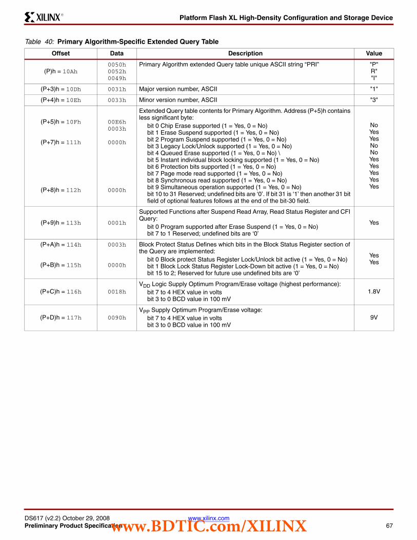
Platform Flash XL High-Density Configuration and Storage Device
DS617 (v2.2) October 29, 2008 www.xilinx.comPreliminary Product Specification 67
R
Table 40: Primary Algorithm-Specific Extended Query Table
Offset Data Description Value
(P)h = 10Ah0050h 0052h 0049h
Primary Algorithm extended Query table unique ASCII string “PRI” "P" R" "I"
(P+3)h = 10Dh 0031h Major version number, ASCII "1"
(P+4)h = 10Eh 0033h Minor version number, ASCII "3"
(P+5)h = 10Fh
(P+7)h = 111h
(P+8)h = 112h
00E6h0003h
0000h
0000h
Extended Query table contents for Primary Algorithm. Address (P+5)h contains less significant byte:
bit 0 Chip Erase supported (1 = Yes, 0 = No) bit 1 Erase Suspend supported (1 = Yes, 0 = No) bit 2 Program Suspend supported (1 = Yes, 0 = No) bit 3 Legacy Lock/Unlock supported (1 = Yes, 0 = No) bit 4 Queued Erase supported (1 = Yes, 0 = No) \bit 5 Instant individual block locking supported (1 = Yes, 0 = No) bit 6 Protection bits supported (1 = Yes, 0 = No) bit 7 Page mode read supported (1 = Yes, 0 = No) bit 8 Synchronous read supported (1 = Yes, 0 = No) bit 9 Simultaneous operation supported (1 = Yes, 0 = No) bit 10 to 31 Reserved; undefined bits are ‘0’. If bit 31 is ‘1’ then another 31 bit field of optional features follows at the end of the bit-30 field.
No Yes Yes No No Yes Yes Yes Yes Yes
(P+9)h = 113h 0001h
Supported Functions after Suspend Read Array, Read Status Register and CFI Query:
bit 0 Program supported after Erase Suspend (1 = Yes, 0 = No) bit 7 to 1 Reserved; undefined bits are ‘0’
Yes
(P+A)h = 114h
(P+B)h = 115h
0003h
0000h
Block Protect Status Defines which bits in the Block Status Register section of the Query are implemented:
bit 0 Block protect Status Register Lock/Unlock bit active (1 = Yes, 0 = No) bit 1 Block Lock Status Register Lock-Down bit active (1 = Yes, 0 = No) bit 15 to 2; Reserved for future use undefined bits are ‘0’
Yes Yes
(P+C)h = 116h 0018hVDD Logic Supply Optimum Program/Erase voltage (highest performance):
bit 7 to 4 HEX value in volts bit 3 to 0 BCD value in 100 mV
1.8V
(P+D)h = 117h 0090hVPP Supply Optimum Program/Erase voltage:
bit 7 to 4 HEX value in volts bit 3 to 0 BCD value in 100 mV
9V
www.BDTIC.com/XILINX

Platform Flash XL High-Density Configuration and Storage Device
DS617 (v2.2) October 29, 2008 www.xilinx.comPreliminary Product Specification 68
R
Table 41: Protection Register Information
Offset Data Description Value
(P+E)h = 118h 0002hNumber of protection register fields in JEDEC ID space. 0000h indicates that 256 fields are available. 2
(P+F)h = 119h 0080h Protection Register 1: Protection Description:Bits 0-7 Lower byte of protection register address Bits 8-15 Upper byte of protection register address Bits 16-23 2n bytes in factory pre-programmed region Bits 24-31 2n bytes in user programmable region
80h
(P+10)h = 11Ah 0000h 00h
(P+ 11)h = 11Bh 0003h 8 bytes
(P+12)h = 11Ch 0003h 8 bytes
(P+13)h = 11Dh 0089h
Protection Register 2: Protection Description: Bits 0-31 protection register address Bits 32-39 n number of factory programmed regions (lower byte) Bits 40-47 n number of factory programmed regions (upper byte) Bits 48-55 2n bytes in factory programmable region Bits 56-63 n number of user programmable regions (lower byte) Bits 64-71 n number of user programmable regions (upper byte) Bits 72-79 2n bytes in user programmable region
89h
(P+14)h = 11Eh 0000h 00h
(P+15)h = 11Fh 0000h 00h
(P+16)h = 120h 0000h 00h
(P+17)h = 121h 0000h 0
(P+18)h = 122h 0000h 0
(P+19)h = 123h 0000h 0
(P+1A)h = 124h 0010h 16
(P+1B)h = 125h 0000h 0
(P+1C)h = 126h 0004h 16
Table 42: Burst Read Information
Offset Data Description Value
(P+1D)h = 127h 0003h
Page-mode read capability bits 0-7 n’ such that 2n HEX value represents the number of read-page bytes. See offset 0028h for device word width to determine page-mode data output width.
8 bytes
(P+1E)h = 128h 0004h Number of synchronous mode read configuration fields that follow. 4
(P+1F)h = 129h 0001h
Synchronous mode read capability configuration 1 bit 3-7 Reserved bit 0-2 n’ such that 2n+1 HEX value represents the maximum number of continuous synchronous reads when the device is configured for its maximum word width. A value of 07h indicates that the device is capable of continuous linear bursts that output data until the internal burst counter reaches the end of the device’s burstable address space. This field’s 3-bit value can be written directly to the read configuration register bit 0-2 if the device is configured for its maximum word width. See offset 0028h for word width to determine the burst data output width.
4
(P+20)h = 12Ah(P-21)h = 12Bh(P+22)h = 12Ch
0002h0003h0007h
Synchronous mode read capability configuration 2 8
Synchronous mode read capability configuration 3 16
Synchronous mode read capability configuration 4 Cont.
Table 43: Bank and Erase Block Region Information(1,2)
Offset Data Description
(P+23)h = 12Dh 02h Number of Bank Regions within the device
Notes: 1. The variable P is a pointer which is defined at CFI offset 015h.2. Bank Regions. There are two Bank Regions, see Table 35, page 61.
www.BDTIC.com/XILINX

Platform Flash XL High-Density Configuration and Storage Device
DS617 (v2.2) October 29, 2008 www.xilinx.comPreliminary Product Specification 69
R
Table 44: Bank and Erase Block Region 1 Information(1,2)
Offset Data Description
(P+24)h = 12Eh 0Fh Number of identical banks within Bank Region 1
(P+25)h = 12Fh 00h
(P+26)h = 130h 11h
Number of program or erase operations allowed in Bank Region 1: Bits 0–3: Number of simultaneous program operations Bits 4–7: Number of simultaneous erase operations
(P+27)h = 131h 00h
Number of program or erase operations allowed in other banks while a bank in same region is programming
Bits 0–3: Number of simultaneous program operations Bits 4–7: Number of simultaneous erase operations
(P+28)h = 132h 00h
Number of program or erase operations allowed in other banks while a bank in this region is erasing
Bits 0–3: Number of simultaneous program operations Bits 4–7: Number of simultaneous erase operations
(P+29)h = 133h 01hTypes of erase block regions in Bank Region 1 n = number of erase block regions with contiguous same-sized erase blocks. Symmetrically blocked banks have one blocking region(2).
(P+2A)h = 134h 07hBank Region 1 Erase Block Type 1 Information:
Bits 0–15: n+1 = number of identical-sized erase blocks Bits 16–31: n×256 = number of bytes in erase block region
(P+2B)h = 135h 00h
(P+2C)h = 136h 00h
(P+2D)h = 137h 02h
(P+2E)h = 138h 64h Bank Region 1 (Erase Block Type 1)Minimum block erase cycles × 1000(P+2F)h = 139h 00h
(P+30)h = 13Ah 01h
Bank Region 1 (Erase Block Type 1): BIts per cell, internal ECC Bits 0–3: bits per cell in erase region Bit 4: reserved for “internal ECC used” BIts 5–7: reserved
(P+31)h = 13Bh 03h
Bank Region 1 (Erase Block Type 1): Page mode and Synchronous mode capabilities Bit 0: Page-mode reads permittedBit 1: Synchronous reads permittedBit 2: Synchronous writes permittedBits 3–7: reserved
– –
Bank Region 1 Erase Block Type 2 InformationBits 0–15: n+1 = number of identical-sized erase blocks Bits 16–31: n×256 = number of bytes in erase block region
Bank Region 1 (Erase Block Type 2)Minimum block erase cycles × 1000
Bank Regions 1 (Erase Block Type 2): Bits per cell, internal ECC Bits 0–3: bits per cell in erase region Bit 4: reserved for “internal ECC used” Bits 5–7: reserved
Bank Region 1 (Erase Block Type 2): Page mode and Synchronous mode capabilities Bit 0: Page-mode reads permitted Bit 1: Synchronous reads permitted Bit 2: Synchronous writes permitted Bits 3–7: reserved
Notes: 1. The variable P is a pointer which is defined at CFI offset 015h.2. Bank Regions. There are two Bank Regions, see Table 35, page 61.
www.BDTIC.com/XILINX

Platform Flash XL High-Density Configuration and Storage Device
DS617 (v2.2) October 29, 2008 www.xilinx.comPreliminary Product Specification 70
R
Table 45: Bank and Erase Block Region 2 Information(1,2)
Offset Data Description
(P+32)h = 13Ch 01hNumber of identical banks within Bank Region 2
(P+33)h = 13Dh 00h
(P+34)h = 13Eh 11hNumber of program or erase operations allowed in Bank Region 2:
Bits 0–3: Number of simultaneous program operations Bits 4–7: Number of simultaneous erase operations
(P+35)h = 13Fh 00h
Number of program or erase operations allowed in other banks while a bank in this region is programming
Bits 0–3: Number of simultaneous program operations Bits 4–7: Number of simultaneous erase operations
(P+36)h = 140h 00h
Number of program or erase operations allowed in other banks while a bank in this region is erasing
Bits 0–3: Number of simultaneous program operations Bits 4–7: Number of simultaneous erase operations
(P+37)h = 141h 02hTypes of erase block regions in Bank Region 2 n = number of erase block regions with contiguous same-sized erase blocks. Symmetrically blocked banks have one blocking region.(2)
(P+38)h = 142h 06hBank Region 2 Erase Block Type 1 Information
Bits 0–15: n+1 = number of identical-sized erase blocks Bits 16–31: n×256 = number of bytes in erase block region
(P+39)h = 143h 00h
(P+3A)h = 144h 00h
(P+3B)h = 145h 02h
(P+3C)h = 146h 64h Bank Region 2 (Erase Block Type 1)Minimum block erase cycles × 1000(P+3D)h = 147h 00h
(P+3E)h = 148h 01h
Bank Region 2 (Erase Block Type 1): Bits per cell, internal ECC Bits 0–3: bits per cell in erase region Bit 4: reserved for “internal ECC used” Bits 5–7: reserved
(P+3F)h = 149h 03h
Bank Region 2 (Erase Block Type 1):Page mode and Synchronous mode capabilities (defined in Table 42, page 68)
Bit 0: Page-mode reads permitted Bit 1: Synchronous reads permitted Bit 2: Synchronous writes permitted Bits 3–7: reserved
(P+40)h = 14Ah 03h
Bank Region 2 Erase Block Type 2 Information Bits 0–15: n+1 = number of identical-sized erase blocks Bits 16–31: n×256 = number of bytes in erase block region
(P+41)h = 14Bh 00h
(P+42)h = 14Ch 80h
(P+43)h = 14Dh 00h
(P+44)h = 14Eh 64h Bank Region 2 (Erase Block Type 2)Minimum block erase cycles × 1000(P+45)h = 14Fh 00h
(P+46)h = 150h 01h
Bank Region 2 (Erase Block Type 2): Bits per cell, internal ECC Bits 0-3: bits per cell in erase region Bit 4: reserved for “internal ECC used” Bits 5–7: reserved
(P+47)h = 151h 03h
Bank Region 2 (Erase Block Type 2): Page mode and Synchronous mode capabilities (defined in Table 42, page 68)
Bit 0: Page-mode reads permitted Bit 1: Synchronous reads permitted Bit 2: Synchronous writes permitted Bits 3–7: reserved
(P+48)h = 152h – Feature Space definitions
(P+49)h = 153h – Reserved
Notes: 1. The variable P is a pointer which is defined at CFI offset 015h. 2. Bank Regions. There are two Bank Regions, see Table 35, page 61.
www.BDTIC.com/XILINX

Platform Flash XL High-Density Configuration and Storage Device
DS617 (v2.2) October 29, 2008 www.xilinx.comPreliminary Product Specification 71
R
Appendix C: Flowcharts and PseudocodesX-Ref Target - Figure 38
Notes: 1. Status check of SR1 (Protected Block), SR3 (VPP Invalid) and SR4 (Program Error) can be made after each program operation or after a sequence.2. If an error is found, the Status Register must be cleared before further Program/Erase Controller operations.3. Any address within the bank can equally be used.4. To read the memory in Asynchronous mode, the CR15 Configuration Register bit must be written to 1.
Figure 38: Program Flowchart and Pseudocode
Write 40h or 10h(3)
Start
Write Address& Data
Read Status Register(3)
YES
NOSR7 = 1
YES
NOSR3 = 0
NOSR4 = 0
VPP InvalidError(1,2)
ProgramError(1,2)
program_command (addressToProgram, dataToProgram) {: writeToFlash (addressToProgram, 0x40); /*writeToFlash (addressToProgram, 0x10);*/ /*see note (3)*/
do { status_register=readFlash (addressToProgram); "see note (3)"; /* E or G must be toggled*/
} while (status_register.SR7== 0) ;
if (status_register.SR3==1) /*VPP invalid error */ error_handler ( ) ;
YES
End
YES
NOSR1 = 0
Program to ProtectedBlock Error(1,2)
writeToFlash (addressToProgram, dataToProgram) ;/*Memory enters read status state after the Program Command*/
if (status_register.SR4==1) /*program error */ error_handler ( ) ;
if (status_register.SR1==1) /*program to protect block error */ error_handler ( ) ;
}DS617_31_101608
www.BDTIC.com/XILINX

Platform Flash XL High-Density Configuration and Storage Device
DS617 (v2.2) October 29, 2008 www.xilinx.comPreliminary Product Specification 72
R
X-Ref Target - Figure 39
Notes: 1. Any address within the bank can equally be used.2. If an error is found, the Status Register must be cleared before further Program/Erase operations.3. To read the memory in Asynchronous mode, the CR15 Configuration Register bit must be written to 1.
Figure 39: Blank Check Flowchart and Pseudocode
Write BlockAddress & BCh
Start
SR7 = 1
Write BlockAddress & CBh
ReadStatus Register(1)
SR4 = 1SR5 = 1
SR5 = 0
NO
YES
Command SequenceError(2)
YES
Blank Check Error(2)NO
End
blank_check_command (blockToCheck) {
writeToFlash (blockToCheck, 0xBC);
writeToFlash (blockToCheck, 0xCB); /* Memory enters read status state after the Blank Check Command */
do { status_register = readFlash (blockToCheck); /* see note (1) */ /* E or G must be toggled */
} while (status_register.SR7==0);
if (status_register.SR4==1) && (status_register.SR5==1) /* command sequence error */ error_handler () ;
if (status_register.SR5==1) /* Blank Check error */ error_handler () ;
}
DS617_32_101608
www.BDTIC.com/XILINX

Platform Flash XL High-Density Configuration and Storage Device
DS617 (v2.2) October 29, 2008 www.xilinx.comPreliminary Product Specification 73
R
X-Ref Target - Figure 40
Notes: 1. n + 1 is the number of data being programmed.2. Next Program data is an element belonging to buffer_Program[].data; Next Program address is an element belonging to
buffer_Program[].address3. Routine for Error Check by reading SR3, SR4 and SR1.4. To read the memory in Asynchronous mode, the CR15 Configuration Register bit must be written to 1.
Figure 40: Buffer Program Flowchart and Pseudocode
Buffer Program E8hCommand,
Start Address
Start
Write Buffer Data,Start Address
YESX = n
End
Write n(1),Start Address
X = 0
Write Next Buffer Data,Next Program Address
X = X + 1
ProgramBuffer to FlashConfirm D0h
Read StatusRegister
NOSR7 = 1
YES
Full Status Register Check(3)
(2)
Read StatusRegister
NOSR7 = 1
YES
Buffer_Program_command (Start_Address, n, buffer_Program[] )/* buffer_Program [] is an array structure used to store the address anddata to be programmed to the Flash memory (the address must be withinthe segment Start Address and Start Address+n) */{do {writeToFlash (Start_Address, 0xE8) ;
status_register=readFlash (Start_Address);
} while (status_register.SR7==0);
writeToFlash (Start_Address, n);
writeToFlash (buffer_Program[0].address, buffer_Program[0].data);/*buffer_Program[0].address is the start address*/
x = 0;
while (x<n)
{ writeToFlash (buffer_Program[x+1].address, buffer_Program[x+1].data);
x++;
}
writeToFlash (Start_Address, 0xD0);
do {status_register=readFlash (Start_Address);
} while (status_register.SR7==0);
full_status_register_check();
}
DS617_33_101608
www.BDTIC.com/XILINX

Platform Flash XL High-Density Configuration and Storage Device
DS617 (v2.2) October 29, 2008 www.xilinx.comPreliminary Product Specification 74
R
X-Ref Target - Figure 41
Notes: 1. The Read Status Register command (Write 70h) can be issued just before or just after the Program Resume command.2. To read the memory in Asynchronous mode, the CR15 Configuration Register bit must be written to 1.
Figure 41: Program Suspend & Resume Flowchart and Pseudocode
Write 70h
Read Status Register
YES
NOSR7 = 1
YES
NOSR2 = 1
Write D0h
Read data fromanother address
Start
Write B0h
Program Complete
Write FFh
program_suspend_command ( ) { writeToFlash (any_address, 0xB0) ;
writeToFlash (bank_address, 0x70) ; /* read status register to check if program has already completed */
do { status_register=readFlash (bank_address) ; /* E or G must be toggled*/
} while (status_register.SR7== 0) ;
if (status_register.SR2==0) /*program completed */
{ writeToFlash (bank_address, 0xFF) ; read_data ( ) ; /*The device returns to Read Array (as if program/erase suspend was not issued).*/
}else { writeToFlash (bank_address, 0xFF) ;
read_data ( ); /*read data from another address*/
writeToFlash (any_address, 0xD0) ; /*write 0xD0 to resume program*/
writeToFlash (bank_address, 0x70) ; /*read status register to check if program has completed */
}}
Write FFh
Program Continues withBank in Read Status
Register Mode
Read Data
Write 70h(1)
DS617_34_101608
www.BDTIC.com/XILINX

Platform Flash XL High-Density Configuration and Storage Device
DS617 (v2.2) October 29, 2008 www.xilinx.comPreliminary Product Specification 75
R
X-Ref Target - Figure 42
Notes: 1. If an error is found, the Status Register must be cleared before further Program/Erase operations.2. Any address within the bank can equally be used.3. To read the memory in Asynchronous mode, the CR15 Configuration Register bit must be written to 1.
Figure 42: Block Erase Flowchart and Pseudocode
Write 20h(2)
Start
Write Block Address & D0h
Read Status Register(2)
YES
NOSR7 = 1
YES
NOSR3 = 0
YESSR4, SR5 = 1
VPP InvalidError(1)
CommandSequence Error(1)
NO
NOSR5 = 0 Erase Error(1)
End
YES
NOSR1 = 0
Erase to ProtectedBlock Error(1)
YES
erase_command ( blockToErase ) { writeToFlash (blockToErase, 0x20) ; /*see note (2) */
writeToFlash (blockToErase, 0xD0) ; /* Memory enters read status state after the Erase Command */
} while (status_register.SR7== 0) ;
do { status_register=readFlash (blockToErase) ; /* see note (2) */ /* E or G must be toggled*/
if (status_register.SR3==1) /*VPP invalid error */ error_handler ( ) ;
if ( (status_register.SR4==1) && (status_register.SR5==1) )/* command sequence error */ error_handler ( ) ;
if (status_register.SR1==1) /*program to protect block error */ error_handler ( ) ;
if ( (status_register.SR5==1) )/* erase error */ error_handler ( ) ;
}DS617_35_101608
www.BDTIC.com/XILINX

Platform Flash XL High-Density Configuration and Storage Device
DS617 (v2.2) October 29, 2008 www.xilinx.comPreliminary Product Specification 76
R
X-Ref Target - Figure 43
Notes: 1. The Read Status Register command (Write 70h) can be issued just before or just after the Erase Resume command.2. To read the memory in Asynchronous mode, the CR15 Configuration Register bit must be written to 1.
Figure 43: Erase Suspend & Resume Flowchart and Pseudocode
Write 70h
Read Status Register
YES
NOSR7 = 1
YES
NOSR6 = 1
Erase Continues
Write D0h
Read data from another block,
Program,
Set Configuration Register or
Block Protect/Unprotect/Lock
Start
Write B0h
Erase Complete
Write FFh
Read Data
Write FFh
erase_suspend_command ( ) { writeToFlash (bank_address, 0xB0) ;
writeToFlash (bank_address, 0x70) ; /* read status register to check if erase has already completed */
do { status_register=readFlash (bank_address) ; /* E or G must be toggled*/
} while (status_register.SR7== 0) ;
if (status_register.SR6==0) /*erase completed */ { writeToFlash (bank_address, 0xFF) ;
read_data ( ) ; /*read data from another block*/ /*The device returns to Read Array (as if program/erase suspend was not issued).*/
}else { writeToFlash (bank_address, 0xFF) ; read_program_data ( ); /*read or program data from another address*/ writeToFlash (bank_address, 0xD0) ; /*write 0xD0 to resume erase*/ }}
DS617_36_101608
www.BDTIC.com/XILINX
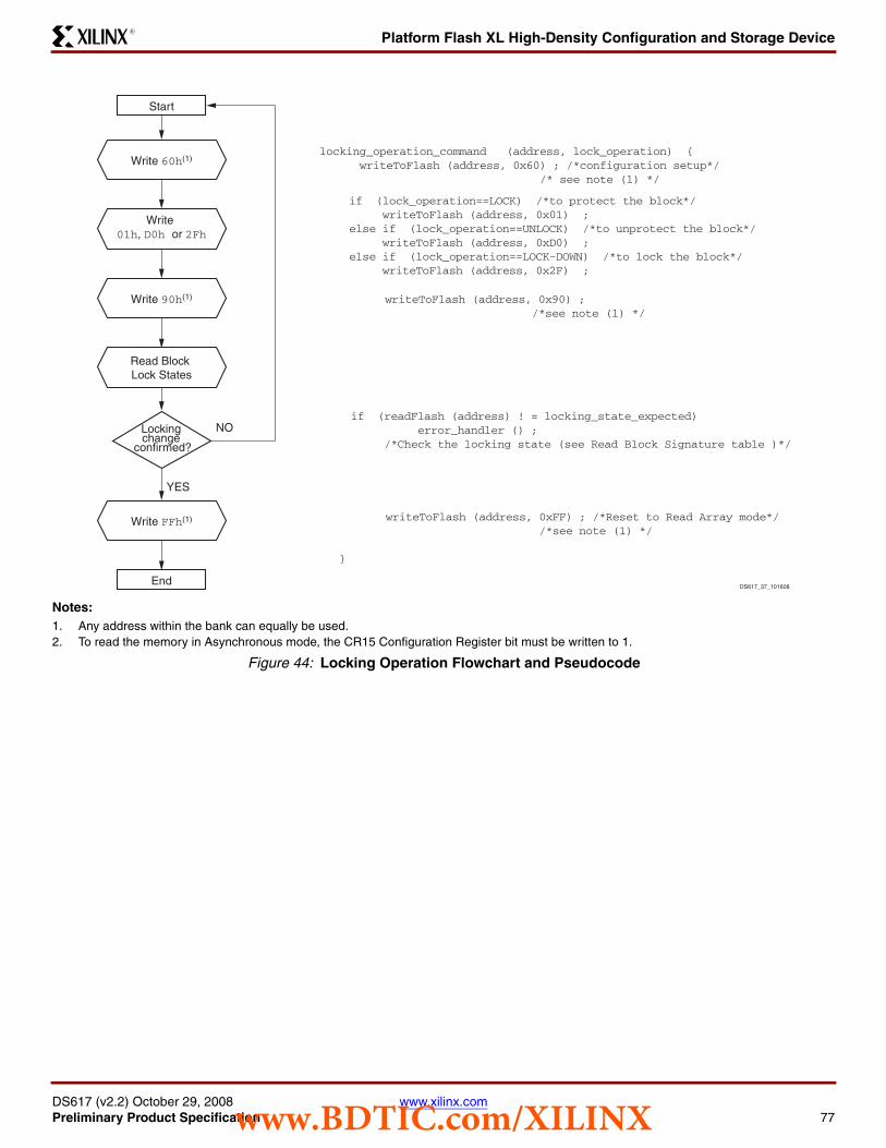
Platform Flash XL High-Density Configuration and Storage Device
DS617 (v2.2) October 29, 2008 www.xilinx.comPreliminary Product Specification 77
R
X-Ref Target - Figure 44
Notes: 1. Any address within the bank can equally be used.2. To read the memory in Asynchronous mode, the CR15 Configuration Register bit must be written to 1.
Figure 44: Locking Operation Flowchart and Pseudocode
Write 01h, D0h or 2Fh
Read Block Lock States
YES
NOLocking change
confirmed?
Start
Write 60h(1)locking_operation_command (address, lock_operation) { writeToFlash (address, 0x60) ; /*configuration setup*/ /* see note (1) */
if (readFlash (address) ! = locking_state_expected) error_handler () ; /*Check the locking state (see Read Block Signature table )*/
writeToFlash (address, 0xFF) ; /*Reset to Read Array mode*/ /*see note (1) */ }
Write FFh(1)
Write 90h(1)
End
if (lock_operation==LOCK) /*to protect the block*/ writeToFlash (address, 0x01) ;else if (lock_operation==UNLOCK) /*to unprotect the block*/ writeToFlash (address, 0xD0) ;else if (lock_operation==LOCK-DOWN) /*to lock the block*/ writeToFlash (address, 0x2F) ;
writeToFlash (address, 0x90) ; /*see note (1) */
DS617_37_101608
www.BDTIC.com/XILINX

Platform Flash XL High-Density Configuration and Storage Device
DS617 (v2.2) October 29, 2008 www.xilinx.comPreliminary Product Specification 78
R
X-Ref Target - Figure 46
X-Ref Target - Figure 45
Notes: 1. Status check of SR1 (Protected Block), SR3 (VPP Invalid) and SR4 (Program Error) can be made after each program operation or after a sequence.2. If an error is found, the Status Register must be cleared before further Program/Erase Controller operations.3. Any address within the bank can equally be used.4. To read the memory in Asynchronous mode, the CR15 Configuration Register bit must be written to 1.
Figure 45: Protection Register Program Flowchart and Pseudocode
Write C0h(3)
Start
Write Address& Data
Read Status Register(3)
YES
NOSR7 = 1
YES
NOSR3 = 0
NOSR4 = 0
VPP InvalidError(1, 2)
ProgramError(1, 2)
protection_register_program_command (addressToProgram, dataToProgram) {: writeToFlash (addressToProgram, 0xC0) ; /*see note (3) */
do { status_register=readFlash (addressToProgram) ; /* see note (3) */ /* E or G must be toggled*/
} while (status_register.SR7== 0) ;
if (status_register.SR3==1) /*VPP invalid error */ error_handler ( ) ;
YES
End
YES
NOSR1 = 0
Program to ProtectedBlock Error(1, 2)
writeToFlash (addressToProgram, dataToProgram) ;/*Memory enters read status state after the Program Command*/
if (status_register.SR4==1) /*program error */ error_handler ( ) ;
if (status_register.SR1==1) /*program to protect block error */ error_handler ( ) ;
}DS617_38_101608
www.BDTIC.com/XILINX

Platform Flash XL High-Density Configuration and Storage Device
DS617 (v2.2) October 29, 2008 www.xilinx.comPreliminary Product Specification 79
R
Notes: 1. To read the memory in Asynchronous mode, the CR15 Configuration Register bit must be written to 1.
Figure 46: Buffer Enhanced Factory Program Flowchart and Pseudocode
Write 80h toAddress WA1
Start
Write D0h toAddress WA1
Write FFFFh to Address = NOT WA1
Read Status Register
SR7 = 0NO
NO
SR0 = 0
YES
Read Status RegisterSR3 and SR1for errors
Exit
Write PDXAddress WA1
Increment CountX = X + 1
Initialize countX = 0
X = 32
YES
Read StatusRegister
Last data?
YES
Read StatusRegister
SR7 = 1
YES
Full Status Register Check
End
YES
SR4 = 1
NO
NO
NO
NO
SETUP PHASE
PROGRAM ANDVERIFY PHASE
EXIT PHASE
Buffer_Enhanced_Factory_Program_Command (start_address, DataFlow[]) {
writeToFlash (start_address, 0x80) ;
writeToFlash (start_address, 0xD0) ;
do {do {status_register = readFlash (start_address);
if (status_register.SR4==1) { /*error*/if (status_register.SR3==1) error_handler ( ) ;/*VPP error */if (status_register.SR1==1) error_handler ( ) ;/* Locked Block */}while (status_register.SR7==1)x=0; /* initialize count */do {
writeToFlash (start_address, DataFlow[x]);
x++;
}while (x<32)do {
status_register = readFlash (start_address);
}while (status_register.SR0==1)
} while (not last data)
writeToFlash (another_block_address, FFFFh)
do {status_register = readFlash (start_address)
}while (status_register.SR7==0)
full_status_register_check();
}DS617_39_101608
www.BDTIC.com/XILINX

Platform Flash XL High-Density Configuration and Storage Device
DS617 (v2.2) October 29, 2008 www.xilinx.comPreliminary Product Specification 80
R
Appendix D: Command Interface State TablesTable 46: Command Interface States – Modify Table, Next State(1)
Current CI State
Command Input
Read
Array
(2)
(FFh
)
Pro
gram
Setu
p(3)(4
) (10/40h
)
Bu
ffer Pro
gram
(3)(4)(E8h
)
Blo
ck Erase,
Setu
p(3)(4) (2
0h
)
BE
FP
Setu
p(80h
)
Blan
k Ch
eck Setu
p(BCh
)
Erase C
on
firm P
/ER
esum
e, Blo
ck Un
lock
Co
nfirm
, BE
FP
C
on
firm(3)(4) (D
0h
)
Blan
k Ch
eck con
firm(CBh)
Bu
ffer Pro
gram
,P
rog
ram/ E
rase Su
spen
d(B0h)
Read
Statu
s Reg
ister(70h
)
Clear S
tatus R
egister (5)
(50h
)
Read
Electro
nic
Sig
natu
re, Read
CF
IQ
uery
Ready Ready Program Setup
BP Setup
Erase Setup
BEFP Setup
Blank Check setup
Ready
Lock/CR Setup Ready (Lock Error)Ready (unlock block)
Ready (Lock Error)
OTP
Setup OTP Busy
Busy OTP Busy
IS in OTP Busy
OTP busy IS in OTP Busy OTP Busy
IS in OTP busy OTP Busy
Program
Setup Program Busy
Busy Program Busy
IS in Program Busy
Program Busy
IS in Program Busy Program Busy Prog.
Susp. Program Busy
IS in Program
BusyProgram Busy
Suspend PS IS in PS PS IS in Program Suspend PS Program
Busy Program Suspend
IS in PS Program Suspend
Buffer Program
Setup Buffer Program Load 1 (give word count load (N-1))
Buffer Load 1 if N=0 go to Buffer Program Confirm. Else (N. 0) go to Buffer Program Load 2 (data load)
Buffer Load 2 Buffer Program Confirm when count =0;Else Buffer Program Load 2(7)
Confirm Ready (error) BP Busy Ready (error)
Busy BP Busy IS in BP Busy BP Busy IS in BP Busy BP Busy BP Susp.
Buffer Program Busy
IS in BP Busy Buffer Program Busy
Suspend BP Suspend IS in BP Suspend
BP Suspen
d
IS in BP
Suspend
BP Suspend BP busy Buffer Program Suspend
IS in BP Suspend Buffer Program Suspend
www.BDTIC.com/XILINX

Platform Flash XL High-Density Configuration and Storage Device
DS617 (v2.2) October 29, 2008 www.xilinx.comPreliminary Product Specification 81
R
Erase
Setup Ready (error) Erase Busy Ready (error)
Busy Erase Busy
IS in Erase Busy
Erase Busy IS in Erase Busy Erase Busy
Erase
Suspend
Erase Busy
IS in Erase Busy
Erase Busy
Suspend Erase Suspend
Program in ES
BP in ES
IS in Erase Suspend ES Erase
Busy Erase Suspend
IS in ES Erase Suspend
Program in Erase Suspend
Setup Program Busy in Erase Suspend
BusyProgram Busy in
ES
IS in Program Busy in
ES
Program Busy in ES
IS in Program Busy in ES Program Busy in ES PS in
ES
Program Busy in Erase Suspend
IS in Program busy in
ES
Program busy in Erase Suspend
Suspend PS in ES IS in PS in ES
PS in ES IS in Program
Suspend in ES PS in ES Program Busy in
ES Program Suspend in Erase Suspend
IS in PS in ES Program Suspend in Erase Suspend
Buffer Program in Erase Suspend
SetupBuffer Program Load 1 in Erase Suspend (give word count load (N-1));
if N=0 go to Buffer Program confirm. Else (N. 0) go to Buffer Program Load 2
Buffer Load 1 Buffer Program Load 2 in Erase Suspend (data load)
Buffer Load 2
Buffer Program Confirm in Erase Suspend when count =0; Else Buffer Program Load 2 in Erase Suspend (note: Buffer Program will fail at this point if any block address is
different from the first address)
Confirm Erase Suspend (sequence error) BP Busy in ES Erase Suspend (sequence error)
Busy BP Busy in ES
IS in BP Busy in
ES
BP busy in
ES
IS in BP busy in ES BP Busy in ES
BP Susp. in ES
Buffer Program Busy in ES
IS in BP busy in
ESBuffer Program Busy in Erase Suspend
Table 46: Command Interface States – Modify Table, Next State(1) (Cont’d)
Current CI State
Command Input
Read
Array
(2)
(FFh
)
Pro
gram
Setu
p(3)(4
) (10/40h
)
Bu
ffer Pro
gram
(3)(4)(E8h
)
Blo
ck Erase,
Setu
p(3)(4) (2
0h
)
BE
FP
Setu
p(80h
)
Blan
k Ch
eck Setu
p(BCh
)
Erase C
on
firm P
/ER
esum
e, Blo
ck Un
lock
Co
nfirm
, BE
FP
C
on
firm(3)(4) (D
0h
)
Blan
k Ch
eck con
firm(CBh)
Bu
ffer Pro
gram
,P
rog
ram/ E
rase Su
spen
d(B0h)
Read
Statu
s Reg
ister(70h
)
Clear S
tatus R
egister (5)
(50h
)
Read
Electro
nic
Sig
natu
re, Read
CF
IQ
uery
www.BDTIC.com/XILINX

Platform Flash XL High-Density Configuration and Storage Device
DS617 (v2.2) October 29, 2008 www.xilinx.comPreliminary Product Specification 82
R
Buffer Program in Erase Suspend(Cont’d)
SuspendBP
Suspend in ES
IS in BP Suspend
in ES
BP Suspend in ES
IS in BP Suspend in
Erase Suspend
BP Suspend
in ES
BP
Busy in
Erase S
uspendBuffer Program Suspend in Erase Suspend
IS in BP Suspend
in ESBP Suspend in Erase Suspend
Blank Check
Setup Ready (error)
Blank
Check busy
Ready (error)
BusyBlank Check busy
IS in Blank Check busy
Blank Check busy
IS in Blank Check busy Blank Check busy
Lock/CR Setup in Erase
Suspend
Erase Suspend (Lock Error) Erase Suspend Erase Suspend (Lock Error)
Buffer EFP
Setup Ready (error) BEFP Busy Ready (error)
Busy BEFP Busy(6)
Notes: 1. CI = Command Interface: CR = Configuration register: BEFP = Buffer Enhanced Factory program: P/E C = Program/Erase controller: IS =
Illegal State: BP = Buffer Program: ES = Erase Suspend.2. At power-up, all banks are in Read Array mode. Issuing a Read Array command to a busy bank, results in undetermined data output.3. The two cycle command should be issued to the same bank address.4. If the P/E C is active, both cycles are ignored.5. The Clear Status Register command clears the SR error bits except when the P/E C. is busy or suspended.6. BEFP is allowed only when Status Register bit SR0 is reset to '0'. BEFP is busy if Block Address is first BEFP Address. Any other commands
are treated as data.7. Buffer Program will fail at this point if any block address is different from the first address.
Table 46: Command Interface States – Modify Table, Next State(1) (Cont’d)
Current CI State
Command Input
Read
Array
(2)
(FFh
)
Pro
gram
Setu
p(3)(4
) (10/40h
)
Bu
ffer Pro
gram
(3)(4)(E8h
)
Blo
ck Erase,
Setu
p(3)(4) (2
0h
)
BE
FP
Setu
p(80h
)
Blan
k Ch
eck Setu
p(BCh
)
Erase C
on
firm P
/ER
esum
e, Blo
ck Un
lock
Co
nfirm
, BE
FP
C
on
firm(3)(4) (D
0h
)
Blan
k Ch
eck con
firm(CBh)
Bu
ffer Pro
gram
,P
rog
ram/ E
rase Su
spen
d(B0h)
Read
Statu
s Reg
ister(70h
)
Clear S
tatus R
egister (5)
(50h
)
Read
Electro
nic
Sig
natu
re, Read
CF
IQ
uery
www.BDTIC.com/XILINX

Platform Flash XL High-Density Configuration and Storage Device
DS617 (v2.2) October 29, 2008 www.xilinx.comPreliminary Product Specification 83
R
Table 47: Command Interface States – Modify Table, Next Output State(1,2)
Current CI State
Command Input
Read
Array
(3) (FFh
)
Pro
gram
Setu
p(4)(5)
(10/40h
)
Bu
ffer Pro
gram
(E8h
)
Blo
ck Erase,
Setu
p(4)(5) (2
0h)
BE
FP
Setu
p (8
0h
)
Blan
k Ch
eck Setu
p (B
Ch
)
Erase C
on
firm P
/E R
esum
e,B
lock U
nlo
ck Co
nfirm
,B
EF
P C
on
firm(4)(5) (D
0h
)
Blan
k Ch
eck con
firm(CBh)
Pro
gram
/ Erase S
usp
end
(B0h
)
Read
Statu
s Reg
ister(70h)
Clear S
tatus R
egister
(50h)
Read
Electro
nic S
ign
ature,
Read
CF
I Qu
ery (90h
, 98h)
Program Setup
Status Register
Erase Setup
OTP Setup
Program Setup in Erase Suspend
BEFP Setup
BEFP Busy
Buffer Program Setup
Buffer Program Load 1
Buffer Program Load 2
Buffer Program Confirm
Buffer Program Setup in Erase Suspend
Buffer Program Load 1 in Erase Suspend
Buffer Program Load 2 in Erase Suspend
Buffer Program Confirm in Erase Suspend
Blank Check setup
Lock/CR Setup
Lock/CR Setup in Erase Suspend
www.BDTIC.com/XILINX

Platform Flash XL High-Density Configuration and Storage Device
DS617 (v2.2) October 29, 2008 www.xilinx.comPreliminary Product Specification 84
R
OTP Busy
Array Status Register Output Unchanged
Status R
egister
Output U
nchanged
Status Register
Ready
Electronic Signature/
CFI
Program Busy
Erase Busy
Buffer Program Busy
Program/Erase Suspend
Buffer Program Suspend
Program Busy in Erase Suspend
Buffer Program Busy in Erase Suspend
Program Suspend in Erase Suspend
Buffer Program Suspend in Erase Suspend
Blank Check busy
Illegal State Output Unchanged
Notes: 1. The output state shows the type of data that appears at the outputs if the bank address is the same as the command address. A bank can
be placed in Read Array, Read Status Register, Read Electronic Signature or Read CFI mode, depending on the command issued. Each bank remains in its last output state until a new command is issued to that bank. The next state does not depend on the bank output state.
2. CI = Command Interface: CR = Configuration Register: BEFP = Buffer Enhanced Factory Program: P/E. C. = Program/Erase Controller.3. At Power-Up, all banks are in Read Array mode. Issuing a Read Array command to a busy bank, results in undetermined data output.4. The two cycle command should be issued to the same bank address.5. If the P/E.C. is active, both cycles are ignored.
Table 47: Command Interface States – Modify Table, Next Output State(1,2) (Cont’d)
Current CI State
Command Input
Read
Array
(3) (FFh)
Pro
gram
Setu
p(4)(5)
(10/40h
)
Bu
ffer Pro
gram
(E8h
)
Blo
ck Erase,
Setu
p(4)(5) (2
0h
)
BE
FP
Setu
p (8
0h
)
Blan
k Ch
eck Setu
p (B
Ch
)
Erase C
on
firm P
/E R
esum
e,B
lock U
nlo
ck Co
nfirm
,B
EF
P C
on
firm(4)(5) (D
0h
)
Blan
k Ch
eck con
firm(CBh)
Pro
gram
/ Erase S
usp
end
(B0h
)
Read
Statu
s Reg
ister(70h)
Clear S
tatus R
egister
(50h)
Read
Electro
nic S
ign
ature,
Read
CF
I Qu
ery (90h, 9
8h
)
www.BDTIC.com/XILINX

Platform Flash XL High-Density Configuration and Storage Device
DS617 (v2.2) October 29, 2008 www.xilinx.comPreliminary Product Specification 85
R
Table 48: Command Interface States – Lock Table, Next State(1)
Current CI State
Command Input
Lock/CR Setup(2) (60h)
OTP Setup(2)
(C0h)
Block Lock
Confirm (01h)
Block Lock-Down
Confirm (2Fh)
Set CR Confirm
(03h)
Block Address (WA0)(3) (XXXXh)
Illegal Command(4)
P/E C Operation
Completed(5)
Ready Lock/CR Setup OTP Setup Ready –
Lock/CR Setup Ready (Lock error) Ready Ready (Lock error) –
OTP
Setup OTP Busy x –
Busy IS in OTP Busy OTP Busy Ready
IS in OTP busy OTP Busy IS Ready
Program
Setup Program Busy –
Busy IS in Program Busy Program Busy Ready
IS in Program busy Program Busy IS Ready
Suspend IS in PS Program Suspend –
IS in PS Program Suspend
Buffer Program
Setup Buffer Program Load 1 (give word count load (N-1) –
Buffer Load 1 Buffer Program Load 2(6) Exit see note (6) –
Buffer Load 2 Buffer Program Confirm when count =0; Else Buffer Program Load 2(9) –
Confirm Ready (error) –
Busy IS in BP Busy Buffer Program Busy Ready
IS in Buffer Program busy Buffer Program Busy IS Ready
Suspend IS in BP Suspend Buffer Program Suspend
–IS in BP Suspend Buffer Program Suspend
Erase
Setup Ready (error) –
Busy IS in Erase Busy Erase Busy Ready
IS in Erase busy Erase Busy IS ready
Suspend Lock/CR Setup in
ES IS in ES Erase Suspend
–
IS in ES Erase Suspend
Program in Erase Suspend
Setup Program Busy in Erase Suspend –
Busy IS in Program busy in ES Program Busy in Erase Suspend ES
IS in Program busy in ES Program Busy in Erase Suspend IS in ES
Suspend IS in PS in ES Program Suspend in Erase Suspend –
IS in PS in ES Program Suspend in Erase Suspend
www.BDTIC.com/XILINX

Platform Flash XL High-Density Configuration and Storage Device
DS617 (v2.2) October 29, 2008 www.xilinx.comPreliminary Product Specification 86
R
Buffer Program in Erase Suspend
Setup Buffer Program Load 1 in Erase Suspend (give word count load (N-1))
–
Buffer Load 1 Buffer Program Load 2 in Erase Suspend(7) Exit see note (7)
Buffer Load 2 Buffer Program Confirm in Erase Suspend when count =0; Else Buffer Program Load 2 in Erase Suspend(9)
Confirm Erase Suspend (sequence error)
Busy IS in BP busy in ES Buffer Program Busy in Erase Suspend ES
IS in BP busy in ES BP busy in ES IS in ES
Suspend IS in BP suspend in ES Buffer Program Suspend in Erase Suspend
–IS in BP Suspend in ES Buffer Program Suspend in Erase Suspend
Blank Check
Setup Ready (error) –
Blank Check busy IS in Blank Check busy Blank Check busy Ready
Lock/CR Setup in ES Erase Suspend(Lock error) Erase Suspend Erase Suspend (Lock error) –
BEFP
Setup Ready (error) –
Busy BEFP Busy(8) Exit BEFP Busy(8) –
Notes: 1. CI = Command Interface: CR = Configuration register: BEFP = Buffer Enhanced Factory program: P/E C = Program/Erase controller: IS =
Illegal State: BP = Buffer program: ES = Erase suspend: WA0 = Address in a block different from first BEFP address.2. If the P/E C is active, both cycle are ignored.3. BEFP Exit when Block Address is different from first Block Address and data are FFFFh.4. Illegal commands are those not defined in the command set.5. –: not available. In this case the state remains unchanged.6. If N = 0 go to Buffer Program Confirm. Else (not = 0) go to Buffer Program Load 2 (data load)7. If N = 0 go to Buffer Program Confirm in Erase suspend. Else (not = 0) go to Buffer Program Load 2 in Erase suspend.8. BEFP is allowed only when Status Register bit SR0 is set to '0'. BEFP is busy if Block Address is first BEFP Address. Any other commands
are treated as data.9. Buffer Program will fail at this point if any block address is different from the first address
Table 48: Command Interface States – Lock Table, Next State(1) (Cont’d)
Current CI State
Command Input
Lock/CR Setup(2) (60h)
OTP Setup(2)
(C0h)
Block Lock
Confirm (01h)
Block Lock-Down
Confirm (2Fh)
Set CR Confirm
(03h)
Block Address (WA0)(3) (XXXXh)
Illegal Command(4)
P/E C Operation
Completed(5)
www.BDTIC.com/XILINX
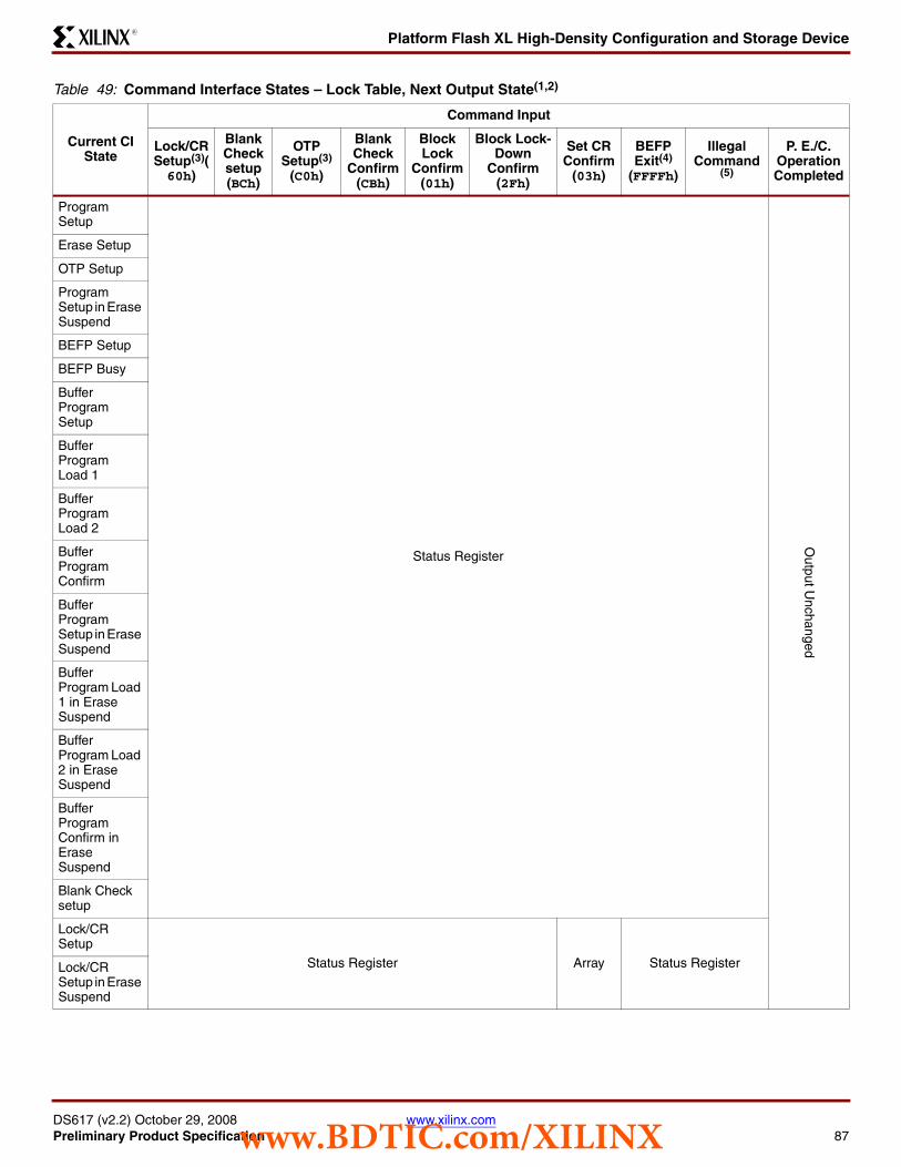
Platform Flash XL High-Density Configuration and Storage Device
DS617 (v2.2) October 29, 2008 www.xilinx.comPreliminary Product Specification 87
R
Table 49: Command Interface States – Lock Table, Next Output State(1,2)
Current CI State
Command Input
Lock/CR Setup(3)(60h)
Blank Check setup (BCh)
OTP Setup(3)
(C0h)
Blank Check
Confirm (CBh)
Block Lock
Confirm (01h)
Block Lock-Down
Confirm (2Fh)
Set CR Confirm
(03h)
BEFP Exit(4)
(FFFFh)
Illegal Command
(5)
P. E./C. Operation Completed
Program Setup
Status Register
Output U
nchanged
Erase Setup
OTP Setup
Program Setup in Erase Suspend
BEFP Setup
BEFP Busy
Buffer Program Setup
Buffer Program Load 1
BufferProgramLoad 2
Buffer Program Confirm
Buffer Program Setup in Erase Suspend
Buffer Program Load 1 in Erase Suspend
Buffer Program Load 2 in Erase Suspend
Buffer Program Confirm in Erase Suspend
Blank Check setup
Lock/CR Setup
Status Register Array Status Register Lock/CR Setup in Erase Suspend
www.BDTIC.com/XILINX
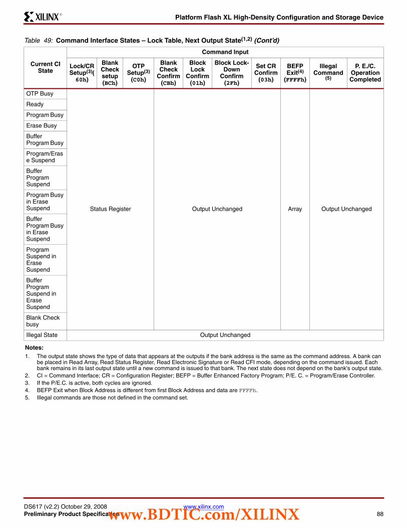
Platform Flash XL High-Density Configuration and Storage Device
DS617 (v2.2) October 29, 2008 www.xilinx.comPreliminary Product Specification 88
R
OTP Busy
Status Register Output Unchanged Array Output Unchanged
Ready
Program Busy
Erase Busy
Buffer Program Busy
Program/Erase Suspend
Buffer Program Suspend
Program Busy in Erase Suspend
Buffer Program Busy in Erase Suspend
Program Suspend in Erase Suspend
Buffer Program Suspend in Erase Suspend
Blank Check busy
Illegal State Output Unchanged
Notes: 1. The output state shows the type of data that appears at the outputs if the bank address is the same as the command address. A bank can
be placed in Read Array, Read Status Register, Read Electronic Signature or Read CFI mode, depending on the command issued. Each bank remains in its last output state until a new command is issued to that bank. The next state does not depend on the bank's output state.
2. CI = Command Interface; CR = Configuration Register; BEFP = Buffer Enhanced Factory Program; P/E. C. = Program/Erase Controller.3. If the P/E.C. is active, both cycles are ignored.4. BEFP Exit when Block Address is different from first Block Address and data are FFFFh.5. Illegal commands are those not defined in the command set.
Table 49: Command Interface States – Lock Table, Next Output State(1,2) (Cont’d)
Current CI State
Command Input
Lock/CR Setup(3)(60h)
Blank Check setup (BCh)
OTP Setup(3)
(C0h)
Blank Check
Confirm (CBh)
Block Lock
Confirm (01h)
Block Lock-Down
Confirm (2Fh)
Set CR Confirm
(03h)
BEFP Exit(4)
(FFFFh)
Illegal Command
(5)
P. E./C. Operation Completed
www.BDTIC.com/XILINX

Platform Flash XL High-Density Configuration and Storage Device
DS617 (v2.2) October 29, 2008 www.xilinx.comPreliminary Product Specification 89
R
Revision HistoryThe following table shows the revision history for this document.
Date Version Revision
12/13/07 1.0 Initial Xilinx release.
03/31/08 2.0 Added bus operations and advance device specifications:• Expanded "Command Interface," page 14, adding new sections.• Added the following sections:
♦ "Status Register," page 23♦ "Configuration Register," page 26♦ "Read Modes," page 34♦ "Dual Operations and Multiple Bank Architecture," page 35♦ "Block Locking," page 37♦ "Power-On Reset," page 39♦ "First Address Latching Sequence," page 41♦ "Program and Erase Times and Endurance Cycles," page 44♦ "Maximum Rating," page 45♦ "DC and AC Parameters," page 45♦ "Appendix A: Block Address Tables," page 61♦ "Appendix B: Common Flash Interface," page 65♦ "Appendix C: Flowcharts and Pseudocodes," page 71♦ "Appendix D: Command Interface State Tables," page 80
Other corrections and updates:• Corrected resistor values in Figure 7, page 10.• Corrected resistor values and removed external resistors from signal K in Figure 8, page 11.• Updated "Marking Information," page 61.
05/14/08 2.1 • Data sheet status changed from Advance to Preliminary.• Corrected the nomenclature for the FT64 package.• Replaced section “FPGA Master BPI-Up Configuration Mode.” with section "Alternate Configuration
Modes," page 11.• Updated Figure 19, page 40 with annotations for TVDDPOR.• Updated Table 21, page 44 to show correct values of VPP.• Updated Table 31, page 58.• Updated trademark references.
10/29/08 2.2 • Minor corrections throughout.• Updated Figure 1, page 2, Figure 8, page 12, Figure 9, page 22, Figure 13, page 31, Figure 16,
page 33, Figure 18, page 39, Figure 19, page 40, and Figure 25, page 46.• Updated Figure 15, page 32, Figure 17, page 33, Figure 21, page 42, Figure 34, page 58, and
Figure 35, page 59 to reflect changed timing parameter nomenclature.• Added maximum rating for junction temperature to Table 22, page 45.• Added Table 24, page 46.• Updated Table 2, page 5, Table 4, page 8, Table 9, page 21, Table 21, page 44, and Table 44,
page 69.• Added new voltage range information to Table 28, page 50.• Updated Table 32, page 59 to reflect changed timing parameter nomenclature.• Updated Table 19, page 42, Table 20, page 43, Table 29, page 52, Table 30, page 56, Table 31,
page 58, and Table 33, page 60. (Added new voltage range information and updated tables to reflect changed timing parameter nomenclature.)
www.BDTIC.com/XILINX

Platform Flash XL High-Density Configuration and Storage Device
DS617 (v2.2) October 29, 2008 www.xilinx.comPreliminary Product Specification 90
R
Notice of DisclaimerTHE XILINX HARDWARE FPGA AND CPLD DEVICES REFERRED TO HEREIN (“PRODUCTS”) ARE SUBJECT TO THE TERMS ANDCONDITIONS OF THE XILINX LIMITED WARRANTY WHICH CAN BE VIEWED AT http://www.xilinx.com/warranty.htm. THIS LIMITEDWARRANTY DOES NOT EXTEND TO ANY USE OF PRODUCTS IN AN APPLICATION OR ENVIRONMENT THAT IS NOT WITHIN THESPECIFICATIONS STATED IN THE XILINX DATA SHEET. ALL SPECIFICATIONS ARE SUBJECT TO CHANGE WITHOUT NOTICE.PRODUCTS ARE NOT DESIGNED OR INTENDED TO BE FAIL-SAFE OR FOR USE IN ANY APPLICATION REQUIRING FAIL-SAFEPERFORMANCE, SUCH AS LIFE-SUPPORT OR SAFETY DEVICES OR SYSTEMS, OR ANY OTHER APPLICATION THAT INVOKESTHE POTENTIAL RISKS OF DEATH, PERSONAL INJURY, OR PROPERTY OR ENVIRONMENTAL DAMAGE (“CRITICALAPPLICATIONS”). USE OF PRODUCTS IN CRITICAL APPLICATIONS IS AT THE SOLE RISK OF CUSTOMER, SUBJECT TOAPPLICABLE LAWS AND REGULATIONS.
www.BDTIC.com/XILINX