xi-3648 mservicio ingles
TRANSCRIPT

Xi3648 (MCA) S/M
SERVICEMANUAL
Published in Nov. ’0034070765Revision 5
R
DIGITAL COPIER

Service Manual

CAUTION
DANGER OF EXPLOSION IF BATTERY IS INCORRECTLY RE-PLACED. REPLACE ONLY WITH THE SAME OR EQUIVALENTTYPE RECOMMENDED BY THE MANUFACTURER. DISPOSEOF USED BATTERIES ACCORDING TO THE MANUFAC-TURER’S INSTRUCTIONS.
ATTENTION
IL Y A DANGER D’EXPLOSION S’IL Y A REMPLACEMENT IN-CORRECT DE LA BATTERIE. REMPLACER UNIQUEMENTAVEC UNE BATTERIE DU MÊME TYPE OU D’UN TYPE REC-OMMANDÉ PAR LE CONSTRUCTEUR. METTRE AU RÉBUTLES BATTERIES USAGÉES CONFORMÉMENT AUX INSTRUC-TIONS DU FABRICANT.

Safety precautions
This booklet provides safety warnings and precautions for our servicepersonnel to ensure the safety of their customers, their machines as wellas themselves during maintenance activities. Service personnel areadvised to read this booklet carefully to familiarize themselves with thewarnings and precautions described here before engaging inmaintenance activities.

Safety warnings and precautions
Various symbols are used to protect our service personnel andcustomers from physical danger and to prevent damage to theirproperty. These symbols are described below:
DANGER: High risk of serious bodily injury or death may result frominsufficient attention to or incorrect compliance with warningmessages using this symbol.
WARNING: Serious bodily injury or death may result from insufficientattention to or incorrect compliance with warning messagesusing this symbol.
CAUTION: Bodily injury or damage to property may result frominsufficient attention to or incorrect compliance with warningmessages using this symbol.
SymbolsThe triangle ( ) symbol indicates a warning including dangerand caution. The specific point of attention is shown insidethe symbol.
General warning.
Warning of risk of electric shock.
Warning of high temperature.
indicates a prohibited action. The specific prohibition isshown inside the symbol.
General prohibited action.
Disassembly prohibited.

indicates that action is required. The specific actionrequired is shown inside the symbol.
General action required.
Remove the power plug from the wall outlet.
Always ground the copier.
1. Installation Precautions
WARNING
• Do not use a power supply with a voltage other than that specified.Avoid multiple connections to one outlet: they may cause fire or electricshock. When using an extension cable, always check that it isadequate for the rated current. ...............................................................
• Connect the ground wire to a suitable grounding point. Not groundingthe copier may cause fire or electric shock. Connecting the earth wireto an object not approved for the purpose may cause explosion orelectric shock. Never connect the ground cable to any of the following:gas pipes, lightning rods, ground cables for telephone lines and waterpipes or faucets not approved by the proper authorities. ........................
CAUTION:
• Do not place the copier on an infirm or angled surface: the copier maytip over, causing injury. ...........................................................................
• Do not install the copier in a humid or dusty place. This may cause fireor electric shock. .....................................................................................
• Do not install the copier near a radiator, heater, other heat source ornear flammable material. This may cause fire. .......................................
• Allow sufficient space around the copier to allow the ventilation grills tokeep the machine as cool as possible. Insufficient ventilation maycause heat buildup and poor copying performance. ...............................

• Always handle the machine by the correct locations when moving it. ....
• Always use anti-toppling and locking devices on copiers so equipped.Failure to do this may cause the copier to move unexpectedly ortopple, leading to injury. ..........................................................................
• Avoid inhaling toner or developer excessively. Protect the eyes. If toneror developer is accidentally ingested, drink a lot of water to dilute it inthe stomach and obtain medical attention immediately. If it gets into theeyes, rinse immediately with copious amounts of water and obtainmedical attention. ....................................................................................
• Advice customers that they must always follow the safety warnings andprecautions in the copier’s instruction handbook. ...................................
2. Precautions for Maintenance
WARNING
• Always remove the power plug from the wall outlet before startingmachine disassembly. ............................................................................
• Always follow the procedures for maintenance described in the servicemanual and other related brochures. ......................................................
• Under no circumstances attempt to bypass or disable safety featuresincluding safety mechanisms and protective circuits. .............................
• Always use parts having the correct specifications. ...............................
• Always use the thermostat or thermal fuse specified in the servicemanual or other related brochure when replacing them. Using a pieceof wire, for example, could lead to fire or other serious accident. ...........
• When the service manual or other serious brochure specifies adistance or gap for installation of a part, always use the correct scaleand measure carefully. ...........................................................................
• Always check that the copier is correctly connected to an outlet with aground connection. .................................................................................

• Check that the power cable covering is free of damage. Check that thepower plug is dust-free. If it is dirty, clean it to remove the risk of fire orelectric shock. .........................................................................................
• Never attempt to disassemble the optical unit in machines using lasers.Leaking laser light may damage eyesight. ..............................................
• Handle the charger sections with care. They are charged to highpotentials and may cause electric shock if handled improperly. .............
CAUTION
• Wear safe clothing. If wearing loose clothing or accessories such asties, make sure they are safely secured so they will not be caught inrotating sections. .....................................................................................
• Use utmost caution when working on a powered machine. Keep awayfrom chains and belts. .............................................................................
• Handle the fixing section with care to avoid burns as it can beextremely hot. .........................................................................................
• Check that the fixing unit thermistor, heat and press rollers are clean.Dirt on them can cause abnormally high temperatures. .........................
• Do not remove the ozone filter, if any, from the copier except forroutine replacement. ...............................................................................
• Do not pull on the AC power cord or connector wires on high-voltagecomponents when removing them; always hold the plug itself. ..............
• Do not route the power cable where it may be stood on or trapped. Ifnecessary, protect it with a cable cover or other appropriate item. ........
• Treat the ends of the wire carefully when installing a new charger wireto avoid electric leaks. ............................................................................
• Remove toner completely from electronic components. .........................
• Run wire harnesses carefully so that wires will not be trapped ordamaged. ................................................................................................

• After maintenance, always check that all the parts, screws, connectorsand wires that were removed, have been refitted correctly. Specialattention should be paid to any forgotten connector, trapped wire andmissing screws. ......................................................................................
• Check that all the caution labels that should be present on the machineaccording to the instruction handbook are clean and not peeling.Replace with new ones if necessary. ......................................................
• Handle greases and solvents with care by following the instructionsbelow: .....................................................................................................· Use only a small amount of solvent at a time, being careful not to
spill. Wipe spills off completely.· Ventilate the room well while using grease or solvents.· Allow applied solvents to evaporate completely before refitting the
covers or turning the main switch on.· Always wash hands afterwards.
• Never dispose of toner or toner bottles in fire. Toner may causesparks when exposed directly to fire in a furnace, etc. .........................
• Should smoke be seen coming from the copier, remove the powerplug from the wall outlet immediately. ..................................................
3. Miscellaneous
WARNING
• Never attempt to heat the drum or expose it to any organic solventssuch as alcohol, other than the specified refiner; it may generate toxicgas. .........................................................................................................

1-1-1
340
CONTENTS
I THEORY AND CONSTRUCTION SECTION1-1 Specifications
1-1-1 Specifications ................................................................................ 1-1-11-2 Handling Precautions
1-2-1 Handling and storage of the drum ................................................. 1-2-11-2-2 Storage of developer and toner ..................................................... 1-2-11-2-3 Handling of the heaters ................................................................. 1-2-11-2-4 Storage of paper ........................................................................... 1-2-1
1-3 Mechanical Construction1-3-1 Part names and functions ............................................................. 1-3-11-3-2 Copy process ................................................................................ 1-3-31-3-3 Machine cross sectional view ........................................................ 1-3-31-3-4 Machine drive system ................................................................... 1-3-41-3-5 Mechanical construction of each section ...................................... 1-3-8
II ELECTRICAL SECTION2-1 Electrical Parts Layout
2-1-1 Electrical parts layout .................................................................... 2-1-12-2 Detection of Paper Misfeed
2-2-1 Paper misfeed detection ............................................................... 2-2-12-2-2 Paper misfeed detection conditions .............................................. 2-2-2
2-3 Operation of the PCBs2-3-1 Power source PCB ........................................................................ 2-3-12-3-2 LPH power supply PCB ................................................................. 2-3-72-3-3 Servo motor control 1 PCB ......................................................... 2-3-102-3-4 Servo motor control 2 PCB ......................................................... 2-3-132-3-5 Main PCB .................................................................................... 2-3-162-3-6 Backup PCB ................................................................................ 2-3-252-3-7 ISU PCB ...................................................................................... 2-3-262-3-8 Operation unit PCB ..................................................................... 2-3-292-3-9 Inverter PCB ................................................................................ 2-3-30
III SET UP AND ADJUSTMENT SECTION3-1 Installation
3-1-1 Unpacking and installing the copier .............................................. 3-1-13-1-2 Copy mode initial settings ........................................................... 3-1-273-1-3 Installing the key counter (optional) ............................................ 3-1-283-1-4 Attaching a roll unit heater (optional) .......................................... 3-1-31
3-2 Simulation3-2-1 Simulation function ........................................................................ 3-2-1
3-3 Assembly and Disassembly3-3-1 Cautions during disassembly and assembly ................................. 3-3-13-3-2 Paper feed section ........................................................................ 3-3-33-3-3 Main charger section ................................................................... 3-3-103-3-4 Exposure and original feed section ............................................. 3-3-193-3-5 Developing section ...................................................................... 3-3-31

1-1-2
340
3-3-6 Transfer/separation section ......................................................... 3-3-373-3-7 Cleaning section .......................................................................... 3-3-423-3-8 Fixing section .............................................................................. 3-3-483-3-9 Other sections ............................................................................. 3-3-60
3-4 PCB Initial Settings3-4-1 Main PCB ...................................................................................... 3-4-13-4-2 Non-field-adjustable volume controls ............................................ 3-4-3
3-5 Self Diagnostics3-5-1 Self-diagnostic function ................................................................. 3-5-1
3-6 Troubleshooting3-6-1 Image formation problems ............................................................ 3-6-13-6-2 Paper misfeeds.. ......................................................................... 3-6-173-6-3 PCB terminal voltages ................................................................. 3-6-233-6-4 Electrical problems ...................................................................... 3-6-383-6-5 Mechanical problems .................................................................. 3-6-51
3-7 AppendixesTiming chart No. 1 ...................................................................................... 3-7-1Timing chart No. 2 ...................................................................................... 3-7-2Timing chart No. 3 ...................................................................................... 3-7-3Timing chart No. 4 ...................................................................................... 3-7-4Timing chart No. 5 ...................................................................................... 3-7-5Main PCB 1/44 ........................................................................................... 3-7-6Main PCB 2/44 ........................................................................................... 3-7-7Main PCB 3/44 ........................................................................................... 3-7-8Main PCB 4/44 ........................................................................................... 3-7-9Main PCB 5/44 ......................................................................................... 3-7-10Main PCB 6/44 ......................................................................................... 3-7-11Main PCB 7/44 ......................................................................................... 3-7-12Main PCB 8/44 ......................................................................................... 3-7-13Main PCB 9/44 ......................................................................................... 3-7-14Main PCB 10/44 ....................................................................................... 3-7-15Main PCB 11/44 ....................................................................................... 3-7-16Main PCB 12/44 ....................................................................................... 3-7-17Main PCB 13/44 ....................................................................................... 3-7-18Main PCB 14/44 ....................................................................................... 3-7-19Main PCB 15/44 ....................................................................................... 3-7-20Main PCB 16/44 ....................................................................................... 3-7-21Main PCB 17/44 ....................................................................................... 3-7-22Main PCB 18/44 ....................................................................................... 3-7-23Main PCB 19/44 ....................................................................................... 3-7-24Main PCB 20/44 ....................................................................................... 3-7-25Main PCB 21/44 ....................................................................................... 3-7-26Main PCB 22/44 ....................................................................................... 3-7-27Main PCB 23/44 ....................................................................................... 3-7-28Main PCB 24/44 ....................................................................................... 3-7-29Main PCB 25/44 ....................................................................................... 3-7-30Main PCB 26/44 ....................................................................................... 3-7-31Main PCB 27/44 ....................................................................................... 3-7-32Main PCB 28/44 ....................................................................................... 3-7-33Main PCB 29/44 ....................................................................................... 3-7-34

1-1-3
340
Main PCB 30/44 ....................................................................................... 3-7-35Main PCB 31/44 ....................................................................................... 3-7-36Main PCB 32/44 ....................................................................................... 3-7-37Main PCB 33/44 ....................................................................................... 3-7-38Main PCB 34/44 ....................................................................................... 3-7-39Main PCB 35/44 ....................................................................................... 3-7-40Main PCB 36/44 ....................................................................................... 3-7-41Main PCB 37/44 ....................................................................................... 3-7-42Main PCB 38/44 ....................................................................................... 3-7-43Main PCB 39/44 ....................................................................................... 3-7-44Main PCB 40/44 ....................................................................................... 3-7-45Main PCB 41/44 ....................................................................................... 3-7-46Main PCB 42/44 ....................................................................................... 3-7-47Main PCB 43/44 ....................................................................................... 3-7-48Main PCB 44/44 ....................................................................................... 3-7-49ISU PCB 1/10 ........................................................................................... 3-7-50ISU PCB 2/10 ........................................................................................... 3-7-51ISU PCB 3/10 ........................................................................................... 3-7-52ISU PCB 4/10 ........................................................................................... 3-7-53ISU PCB 5/10 ........................................................................................... 3-7-54ISU PCB 6/10 ........................................................................................... 3-7-55ISU PCB 7/10 ........................................................................................... 3-7-56ISU PCB 8/10 ........................................................................................... 3-7-57ISU PCB 9/10 ........................................................................................... 3-7-58ISU PCB 10/10 ......................................................................................... 3-7-59Backup PCB ............................................................................................. 3-7-60Servo motor control 1 PCB 1/3 ................................................................. 3-7-61Servo motor control 1 PCB 2/3 ................................................................. 3-7-62Servo motor control 1 PCB 3/3 ................................................................. 3-7-63Output PCB .............................................................................................. 3-7-64LPH power supply PCB ............................................................................ 3-7-65Servo motor control 2 PCB ....................................................................... 3-7-66Operation unit PCB ................................................................................... 3-7-67Power source PCB 1/2 ............................................................................. 3-7-68Power source PCB 2/2 ............................................................................. 3-7-69Detachable unit wiring diagram ................................................................ 3-7-70General connection diagram .................................................................... 3-7-71General wiring diagram ............................................................................ 3-7-72

Xi3648 (MCA) S/M
I The
ory
and
Con
stru
ctio
n Se
ctio
n
THEORY ANDCONSTRUCTION
SECTION
I

1-1-5
340
CONTENTS
1-1 Specifications
1-1-1 Specifications ...................................................................................... 1-1-1
340
1-1-1
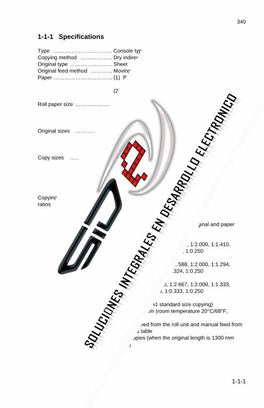
1-1-1 Specifications
Type …………………………… Console typeCopying method ……………… Dry indirect electrostatic photocopyingOriginal type …………………… SheetOriginal feed method ………… Moving originalsPaper …………………………… (1) Plain paper: 64 – 80 g/m2 (fed from the roll unit or
bypass table)(2) Special paper: Tracing paper, film (fed from the roll
unit or bypass table)Roll paper size ………………… Width: 420 – 920 mm/17" – 36"
Diameter: 180 mm/61/4" maximumInner diameter: 76 mm/3"Length: 175 m
Original sizes ………………… Standard: A0 – A4R (64 – 80 g/m2)36" × 48" – 81/2" × 11" (64 – 80 g/m2)
Maximum: 920 (w) × 5,000 (l) mm (64 – 80 g/m2)36" × 197" (64 – 80 g/m2)
Copy sizes …………………… Standard: A0 – A4R (64 – 80 g/m2)36" × 48" – 81/2" × 11" (64 – 80 g/m2)
Maximum: 920 (w) × 5,000 (l) mm (64 – 80 g/m2)36" × 197" (64 – 80 g/m2)
Effective image width: 920 mmLeading edge margin: 5 ± 4 mm
Copying magnificationratios …………………………… Manual mode: 25 – 400%
(at intervals of 1% or 0.1%)Auto copy mode:
Fixed ratios according to the original and papersizes
Metric:1:1±0.5%, 1:4.000, 1:2.829, 1:2.000, 1:1.410,1:0.706, 1:0.500, 1:0.352, 1:0.250
Inch (Architecture):1:1±0.5%, 1:3.143, 1:2.588, 1:2.000, 1:1.294,1:0.640, 1:0.500, 1:0.324, 1:0.250
Inch (Engineer):1:1±0.5%, 1:4.000, 1:2.667, 1:2.000, 1:1.333,1:0.667, 1:0.500, 1:0.333, 1:0.250
Copying speed ………………… 4.8 m/minFirst copy time ………………… 30 s maximum (A1 standard size copying)Warmup time ………………… 10 min maximum (room temperature 20°C/68°F,
65% RH)Paper feed system …………… Automatic feed from the roll unit and manual feed from
the bypass tableConsecutive copying ………… 1 – 20 copies (when the original length is 1300 mm
or less)

340-1
1-1-2
Photoconductor ……………… OPC (Drum diameter: 90 mm)Charging system ……………… Single plus corona charging
Drum surface potential: 870 ± 50 V DCExposure system ……………… Moving original scanningLight source …………………… Fluorescent lamp, 65 WDeveloping system …………… Dry (magnetic brush)
Developer: Dual-component (ferrite carrier and blacktoner: N22T)Toner density control: Toner sensorToner replenishing: Automatic supply from the tonerhopper
Transfer system ……………… Single negative corona charging: –5.3 kV DCSeparation system …………… Single AC corona charging: 5.6 kV ACFixing system ………………… Heat roller
Heat source: Halogen heaters120 V areas: 800 W (main), 400 W (sub)220 – 240 V areas: 1120 W (main), 480 W (sub)Control temperature: 150°C/302°F (plain paper or film)145°C/293°F (tracing paper)Abnormal temperature increase-prevention device:Thermostat, 145°C/293°FFixing pressure: 2.0 N at both ends, 5.9 N at center
Charge erasing system ……… Exposure by cleaning lampCleaning system ……………… Cleaning blade and cleaning fur brushFunctions ……………………… (1) Preheat/energy saving
(2) Auto clear (can be set to between 30 and 270 s atintervals of 30 s)
(3) Auto shutoff (can be set to between 15 and120 min at intervals of 15 min)
(4) Self-diagnostics(5) Simulation(6) Margin copy(7) Hanging copy(8) Program copy(9) Preview copy
(10) Paper cut length setting(11) Same-size/full-size magnification adjustment(12) Fixing temperature adjustment(13) Initial settings change(14) Original size detection(15) Paper size detection
Power requirement …………… 120 V AC, 60 Hz, 13 A220 – 240 V AC, 50/60 Hz, 8 A
Power consumption …………… 1500 W (120 V areas)1900 W (220 – 240 V areas)
Machine dimensions ………… 1355 (w) × 635 (d) × 1107 (h) mm533/8" (w) × 25" (d) × 439/16" (h)
Weight ………………………… Approx. 268 kg, 590.3 lb. (main unit only)Floor requirement …………… 1355 (w) × 707 (d) mm, 533/8" (w) × 2713/16" (d)

340
1-1-3
Accessories …………………… Original reversing guideOptional accessories ………… 3rd roll unit, roll shaft, carrier sheets (A0, A1, A2), key
counter and original support
3rd roll unit (optional)Type …………………………… Built-in typePaper …………………………… Equivalent to the copier to be connected toPower source ………………… Electrically connected to the copier

1-1-7
340
CONTENTS
1-2 Handling Precautions
1-2-1 Handling and storage of the drum ....................................................... 1-2-11-2-2 Storage of developer and toner .......................................................... 1-2-11-2-3 Handling of the heaters ....................................................................... 1-2-11-2-4 Storage of paper ................................................................................. 1-2-1

340
1-2-1
1-2-1 Handling and storage of the drumUse the following caution when handling the drum.• When removing the drum from the main unit, make sure not to expose it to direct sunshine
or strong lighting.• Store the drum where the ambient temperature is kept between –20°C/–4°F and 40°C/
104°F and humidity around 85%RH. Sudden changes in temperature and humidity evenwithin the permitted ranges should be avoided, too.
• Avoid atmosphere laden with substances that might chemically damage the drum surface.• Never hit the drum surface with anything hard or pointed. Protect it from bare or gloved
hands; if it is accidentally touched, clean by following the proper procedure.
1-2-2 Storage of developer and tonerStore developer and toner in a cool, dark place free from direct sunshine or high humidity.
1-2-3 Handling of the heatersThis copier is equipped with heaters to avoid condensation inside. These heaters are keptpowered as long as the copier power cable is connected to a wall outlet with the main switchset off. Never disconnect the power cable if the copier is used in a humid place of 70%RHhigher.If the copier is not going to be used for long periods of time, disconnect the power cable fromthe wall outlet.Each roll unit of this copier is equipped with a roll unit heater*1 which can be individuallyturned on or off with a switch. If normal plain paper is kept in the roll units and there is a riskof high humidity, keep their heaters on. However, keep the heater off if tracing paper is keptin the roll unit.
1-2-4 Storage of paperPaper should be stored in a cool, dark place free from high temperature or humidity. If it isnot going to be used for a long time, take paper out of the roll unit, put it in the originalwrapping paper and seal.
*1 Optional for 220 – 240 V models.
1-1-9
340
CONTENTS
1-3 Mechanical Construction
1-3-1 Part names and functions ................................................................... 1-3-11-3-2 Copy process ...................................................................................... 1-3-31-3-3 Machine cross sectional view ............................................................. 1-3-31-3-4 Machine drive system ......................................................................... 1-3-4
(1) Drive system 1 (driven by the paper feed motor) ........................ 1-3-4(2) Drive system 2 (driven by the paper feed motor) ........................ 1-3-5(3) Drive system 3 (driven by the drum motor and fixing
drive motor) ................................................................................. 1-3-6(4) Drive system 4 (driven by the drive motor and toner
feed motor) .................................................................................. 1-3-6(5) Drive system 5 (driven by the original feed motor) ...................... 1-3-7
1-3-5 Mechanical construction of each section ............................................ 1-3-8(1) Paper feed section ...................................................................... 1-3-8
Winding operation of paper roll ................................................. 1-3-10(1-1) Bypass paper feed .......................................................... 1-3-12(1-2) Roll unit paper feed ........................................................ 1-3-13
(2) Main charger section ................................................................. 1-3-15Drum surface potential correction ............................................. 1-3-18
(3) Exposure and original feed section ........................................... 1-3-19(4) CIS and LPH section ................................................................. 1-3-22
Original image reading .............................................................. 1-3-24Static latent image formation ..................................................... 1-3-24CIS correction ............................................................................ 1-3-26
(5) Developing section .................................................................... 1-3-28Forming the magnetic brush ...................................................... 1-3-29Temperature compensation of the toner sensor output ............ 1-3-30Toner sensor output correction based on the copy count ......... 1-3-31Toner density control ................................................................. 1-3-32
(6) Transfer/separation section ....................................................... 1-3-33(7) Cleaning section ........................................................................ 1-3-36(8) Static eliminator section ............................................................ 1-3-39(9) Fixing section ............................................................................ 1-3-41
Heating and temperature control of heat roller andpress roller ................................................................................. 1-3-43

340
1-3-1
1 Main switch2 Total counter3 Front covers4 Carrier sheet guides5 Copy bins6 Bypass slot7 Bypass table8 Main body release levers9 Original guide0 Paper eject guides
! Original table@ Original loop guide# Original insert slot$ Copy eject slot% Operation panel^ Right cover& Key counter*1
* Copy ready indicator(ready lamp)
( Fuser release button
) Original holding section⁄ Original holder anchor pins¤ Upper rear cover screws‹ Upper rear cover› Transport knobfi Waste toner tankfl Copy bin stopper plates‡ Second roll unit— First roll unit· Instruction handbook box
‚ Roll unit handleŒ Paper roll insertion cover„ Paper roll insertion latches´ Roll unit heater switch*2
‰ Paper roll shaftˇ Paper roll size labelÁ Paper roll release lever¨ Paper roll shaft gearˆ Copy eject slot guides
1-3-1 Part names and functions
Figure 1-3-1
12
3
4
5 6 7
8
9
0 ! @#$ %
^&ˆ
ˆ
8
3
·
fi › °
„
‡ Œ‚fl
´
¨
‰
Á
ˇ
*1 Optional.*2 Optional for 220 – 240 V models.
340-3
1-3-2
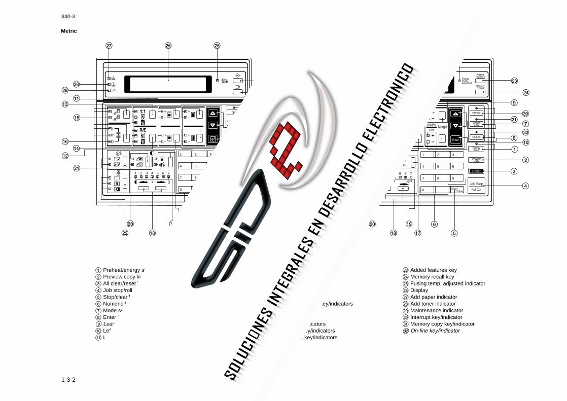
Metric Inch
1 Preheat/energy saver key/indicator2 Preview copy key3 All clear/reset key4 Job stop/roll cut key5 Stop/clear key6 Numeric keys7 Mode set keys8 Enter key9 Leading edge margin key/indicators0 Left margin key/indicators! Leading edge hanging key/indicators
Figure 1-3-2 Operation panel
@ Trailing edge hanging key/indicators# Copy mode select key/indicators$ Zoom mode select key/indicators% Paper length key/indicators^ Paper source key/indicators& Auto/manual contrast select key/indicators* Copy contrast keys( Copy contrast indicators) Original contrast key/indicators⁄ Special paper select key/indicators¤ Image process select key/indicators
‹ Added features key› Memory recall keyfi Fusing temp. adjusted indicatorfl Display‡ Add paper indicator— Add toner indicator· Maintenance indicator‚ Interrupt key/indicatorŒ Memory copy key/indicator„ On-line key/indicator
1 2 3
4 5 6
7 8 9
0 .
1 2 3 4 5 6 7
1
2
3
‡ fl fi
°·
!#
%
^$
@
⁄
¤
)
*
(
&
6
5
‹
›
9‚
Œ
7
81
02
3
4
„
Add Paper
Add Toner
Mainte- nance
Added Features
Fusing Temp. Adjusted
Memory Recall
1 2 3
4 5 6
7 8 9
0 .
1 2 3 4 5 6 7
1
2
3
Memory Copy
Interrupt
Energy Saver
Preview Copy
Reset
Job Stop
Roll CutStopClear
Bold PrintLight Print
Copy Contrast
Auto
Half Tone
Dark Light
Vellum
Film
Material
Border Erase
Negative
Mirror
Image Process
Paper Length
Synchro
Paper Source
Full Size
APS
AMS
Zoom
Preset R E
Indepen- dent Zoom
LeadingEdge
Trailing Left
LeadingMargin
Enter
‡ fl fi
°·
!#
%
^
$@
⁄
¤
)
*
(
&
6
5
‹
›
9
‚Œ
7
8
10
2
3
4
On-Line„
340
1-3-3
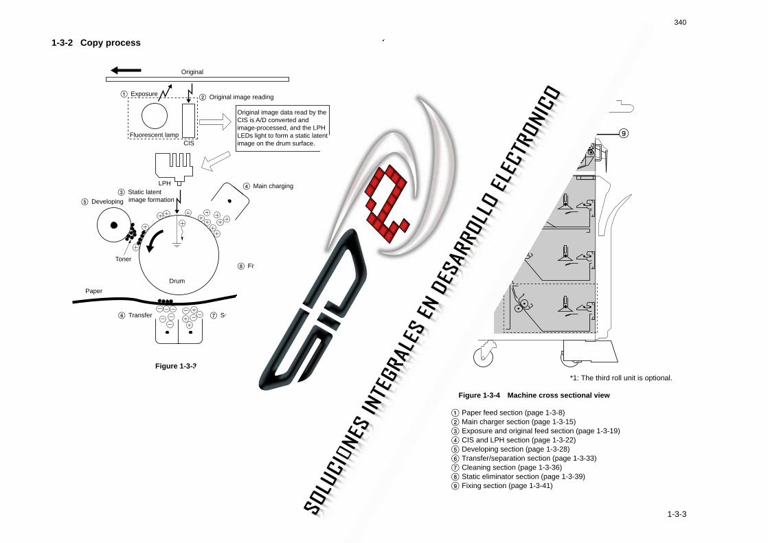
1-3-2 Copy process
Figure 1-3-3 Copy process
1-3-3 Machine cross sectional view
*1: The third roll unit is optional.
1 Paper feed section (page 1-3-8)2 Main charger section (page 1-3-15)3 Exposure and original feed section (page 1-3-19)4 CIS and LPH section (page 1-3-22)5 Developing section (page 1-3-28)6 Transfer/separation section (page 1-3-33)7 Cleaning section (page 1-3-36)8 Static eliminator section (page 1-3-39)9 Fixing section (page 1-3-41)
Original
1 Exposure 2 Original image reading
3 Static latent image formation
4 Main charging
5 Developing
6 Transfer 7 Separation
8 Fixing
Fluorescent lamp CIS
LPH
Paper
Drum
Toner
Original image data read by the CIS is A/D converted and image-processed, and the LPH LEDs light to form a static latent image on the drum surface.
4
3 2 8 7
9
8
5
6
1
Figure 1-3-4 Machine cross sectional view

340-1
1-3-4
1-3-4 Machine drive system
(1) Drive system 1 (driven by the paper feed motor)
Figure 1-3-5 Drive system 1 (outer side to the left frame)
1 Paper feed motor pulley 15/182 Cutter drive belt3 Drive tension pulley4 Cutter drive pulley 205 SB gear 376 Cutter clutch gear7 Cutter drive gear 218 Duplex gear 329 Paper feed section drive belt 10 Drive tension pulley! Paper feed pulley 16@ Pre-transfer drive gear# Optical section idle gear 46$ Roll paper conveying clutch gear% Idle gear 45^ Paddle gear& Optical section idle gear 46* SB gear 37
( Bypass registration clutch gear) Gear 50T⁄ Registration clutch gear¤ Paper feed pulley 16‹ Idle gear 36/30› Middle feed clutch gearfi Optical section idle gear 46fl Idle gear 20/26‡ Middle roll winding clutch gear— Pulley 20P5· Paper feed section drive belt 2*1
‚ Pulley 20P5*1
ΠPaper feed pulley 16*1
„ Idle gear 36/30*1
´ Lower feed clutch gear*1
‰ Optical section idle gear 46*1
ˇ Idle gear 20/26*1
Á Lower roll winding clutch gear*1
*1: Parts 29 to 36 are present when the third roll unit (optional) is installed.
¤
⁄
‹› fi
fl
‡
·
°
) (
8
!
@#
$ %^
&
*
0
9
7
6
54
3
2
1
Œ
„´
‰ˇ
Á‚

340-1
1-3-5
(2) Drive system 2 (driven by the paper feed motor)
1 Cutter drive gear 212 Cutter gear 323 Eject gear 294 Fixing unit idle gear 24T5 Duplex gear 326 Drive gear 20T7 Drive gear 20T8 Paper feed pulley gear B9 Paper feed pulley gear B0 Idle gear 22! Paper feed pulley gear B@ Upper roll winding clutch gear# Drive gear 20T
$ Idle gear 16/25% Duplex gear 32^ Roll idle gear A& Spiral roller gear 23* Roll gear 40( Duplex gear 32) Upper feed clutch gear⁄ Drive gear 20T¤ Roll drive gear 16‹ Roll gear 40› Roll drive gear 16*1
fi Roll gear 40*1
*1: Parts 24 and 25 are present when the third roll unit (optional) is installed.
Figure 1-3-6 Drive system 2 (inner side from the left frame)
1
2
43
5
67 8
9
0
!@#
$
%^&
*
(
)
⁄
¤ ‹
fi›

340
1-3-6
(3) Drive system 3 (driven by the drum motor and fixing drive motor) (4) Drive system 4 (driven by the drive motor and toner feed motor)
Figure 1-3-8 Drive system 4 (inner side from the left frame)
1 Main drive pulley2 Drive tension pulley3 Pre-transfer drive belt4 Pre-transfer drive pulley 325 Developer gear6 Drum motor gear 177 Drum drive gear 458 Drum drive gear 609 Developing unit drive belt0 Tension pulley! Developing unit drive pulley 16@ Fixing drive motor gear
# Fixing section drive gear$ Developer gear 22% Idle gear 34^ Idle gear 26& SB gear 24* Heat roller gear( Fixing gear 24) Idle gear 22⁄ Sleeve gear 17¤ Fixing unit idle gear‹ Gear 27T
1 Pre-transfer drive gear 222 Drive gear 20T3 Pre-transfer gear 304 Drum joint5 Left drum flange6 Feed gear 257 Fur brush gear 178 Roll unit gear 189 Developing unit drive gear 200 Developing roller gear 19! Developing unit idle gear 17
@ Developer paddle gear# Spiral roller gear 23$ Toner shaft gear% Toner shaft gear^ Fixing idle gear
(left side of the machine)& Toner feed motor gear
(right side of the machine)* Toner gear 34( Toner gear 34
67
8
5
!
9
432
1
0)
(¤
*
%
#
$&
⁄
‹
@
Figure 1-3-7 Drive system 3 (outer side to the left frame)
13
248
7
590!
^&
*(
$%
#@
6

340
1-3-7
(5) Drive system 5 (driven by the original feed motor)
Figure 1-3-9 Drive system 5 (outer side to the right frame)
1 Original feed motor pulley2 Original feed drive belt 13 Idle pulley 164 Tension pulley5 Original feed clutch gear6 Developing unit pulley
7 Front lower original roller8 Front upper original roller9 Original feed pulley0 Original feed drive belt 2! Original feed pulley
4 3 21
6!09
8
7
5

340
1-3-8
1-3-5 Mechanical construction of each section
(1) Paper feed sectionThe paper feed section is comprised of the parts shown in Figure 1-3-10. Paper can be fedeither manually or automatically from a paper roll.In the paper feed section, a sheet of paper fed from the roll unit or placed on the bypass tableis conveyed to the transfer section in synch with the LED on timing of the LPH section.
Figure 1-3-10 Paper feed section
1
@
#
›
‰
fi
4
$
‹
fl
ˇ
)
36
!
„
¨
Ø
∏
%
5
&
^
‡
ˆ
°
⁄
27
Å
(
¤
Á
*
8
9
‚
´
Œ
0
·

340
1-3-9
Figure 1-3-11 Block diagram of the paper feed section
*1 Parts 34 to 41 are present when the third roll unit (optional) is installed.
1 Registration upper guide2 Bypass pulley3 Registration lower guide4 Bypass table5 Bypass registration roller6 Registration roller7 Cutter eject rear guide8 Registration pulley9 Cutter unit0 Cutter rear guide! Cutter front guide@ Roll lever# Roll base A$ Paper roll shaft% Roll paper feed upper guide A^ Roll paper feed upper roller& Roll paper feed lower roller A* Roll paper conveying rear roller A( Roll paper conveying front roller) Roll stay A⁄ Roll paper feed lower guide A
¤ Roll paper conveying upper guide‹ Center partition› Roll leverfi Roll base Bfl Paper roll shaft‡ Roll paper feed upper guide B— Roll paper feed upper roller· Roll front guide B‚ Roll rear guide BŒ Roll paper conveying rear roller B„ Roll paper conveying lower guide´ Roll paper conveying rear guide‰ Roll lever*1
ˇ Paper roll shaft*1
Á Roll base B*1
¨ Roll paper feed upper guide B*1
ˆ Roll paper feed upper roller*1
Ø Roll front guide B*1
” Roll rear guide B*1
Å Roll paper conveying rear roller C*1
CN3-14 CN3-34
CN6-14
CN3-1
CN3-5DCM2PCB
CN6-7
CN3-11CN6-8
CN7-13CN6-9CN3-9CN4-8ACN3-10
CN7-14
CN3-26CN3-28CN3-29CN6-10CN7-16
CN7-15
CN6-12CN7-17CN6-13
CN4-9A
CN6-11
MPCB
BYP RCL
RCL
RSW
RPCCL
PS-M
RWCL-M
PS-L
RWCL-L
PFM
FCL-M
FCL-L
FCL-U RWCL-U
RLDSW-U
CCL
BY
PR
SW
BY
PT
IMS
W
PFM ENAPFM SPEED2PFM SPEED1
CN7-12
RLDSW-L
CHPSW1CHPSW2
PS-U
RLDSW-M

340
1-3-10
Winding operation of paper roll
The leading edge of the paper in the roll unit is first fed to the home position (copy readyposition) by the winding operation, where it is ready for copying.
• After the following operations, if the leading edge of the paper roll is not at the homeposition, the winding operation for that roll unit will be performed.
1) After pressing the all clear/reset key.2) After performing the auto clear function.3) After changing the paper feed position with the paper source key.4) One minute after a copy cycle ends and the ready lamp (copy ready indicator) lights.
(If any key is pressed after the ready lamp is lit, another minute will be counted afterthe key press.)
5) After opening/closing the right cover (cycling safety switch 3), the main body(cycling safety switches 4 and 5), or the upper rear cover (cycling safety switch 6).
• After the following operation, the winding operation for all the roll units will be performed.(Winding starts with the lowest roll unit.)
1) After opening/closing the front covers (cycling safety switches 1 and 2).
• With the roll paper leading edge detection switch off
Timing chart 1-3-1 Winding operation for the first roll unit (1)
a The paper feed motor (PFM) and the upper feed clutch (FCL-U) turn on, and the paperis conveyed in the feed direction.
b The upper feed clutch (FCL-U) and the paper feed motor (PFM) are turned off 100 msafter the upper roll paper leading edge detection switch (RLDSW-U) is turned on, andthe leading edge of the paper stops at the home position (copy ready position).• Winding operation for the 2nd and 3rd roll units is performed similarly.
OnPFM
RLDSW-U100 ms
Off
On
Off
Off
OnFCL-U
a
b

340
1-3-11
• With the roll paper leading edge detection switch on
Timing chart 1-3-2 Winding operation for the first roll unit (2)
a The paper feed motor (PFM) and the upper roll winding clutch (RWCL-U) are turned on,and the paper starts to wind.
b After the upper roll paper leading edge detection switch (RLDSW-U) turns off, the upperroll winding clutch (RWCL-U) turns off and the upper feed clutch (FCL-U) turns on, andthe paper is conveyed in the feed direction.
c 100 ms after the upper roll paper leading edge detection switch (RLDSW-U) turns on,the upper feed clutch (FCL-U) and the paper feed motor (PFM) turn off, and the leadingedge of the paper stops at the home position (copy ready position).• Winding operation for the 2nd and 3rd roll units is performed similarly.
Off
On
OnPFM
RLDSW-U100 ms
Off
On
OffOff
On
RWCL-U
FCL-U
a
b
c

340
1-3-12
(1-1) Bypass paper feed
Timing chart 1-3-3 Bypass paper feed
a 1.75 s after the bypass registration switch (BYPRSW) is turned on by inserting paper intothe bypass table, the paper feed motor (PFM) and the bypass registration clutch(BYPRCL) turn on, and feeding of the inserted paper starts.
b 750 ms after the bypass timing switch (BYPTIMSW) turns on, the bypass registrationclutch (BYPRCL) turns off, and the paper stops at the copy ready position.
c Potential buildup, primary original feed and then shading correction are completed. 450ms after these secondary paper feed start conditions are satisfied, the PSYNC signalturns on.
d The bypass registration clutch (BYPRCL) turns on to convey the paper to the transfersection.
e 200 ms after the paper is conveyed to the transfer section and the bypass timing switch(BYPTIMSW) turns off, the bypass registration clutch (BYPRCL) turns off, and the paperfeed operation is completed.
1.75 s
Off
Off
Off
PFM
BYPRCL
OLDSW
BYPRSW
OTDSW
BYPTIMSW
750 ms
Off
Off
On
On
On
On
Off
On
OnOff
BYPRSW: On
BYPTIMSW: On
OLDSW: On
OTDSW: On
BYPTIMSW: Off
a b200 ms574 ms
450 ms
e
c
d
PSYNC signal
Paper insertion
Original insertion
Potential buildup completed. Primary original feed completed. Shading correction completed.
With the paper inserted before the original.
340
1-3-13
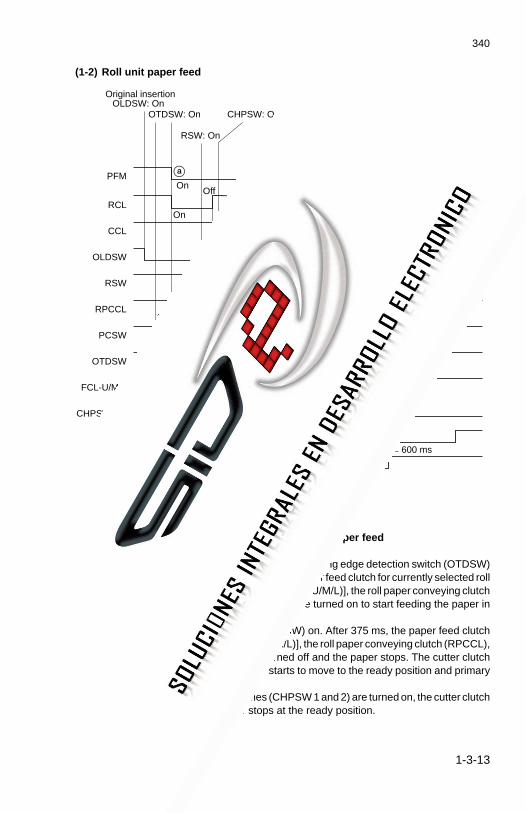
(1-2) Roll unit paper feed
Timing chart 1-3-4 Roll unit paper feed
a 1 s after the original is inserted and the original trailing edge detection switch (OTDSW)is turned on, the paper feed motor (PFM), the paper feed clutch for currently selected rollunit [the upper/middle/lower feed clutches (FCL-U/M/L)], the roll paper conveying clutch(RPCCL), and the registration clutch (RCL) are turned on to start feeding the paper inthe selected roll unit.
b The paper turns the registration switch (RSW) on. After 375 ms, the paper feed clutch[upper/middle/lower feed clutch (FCL-U/M/L)], the roll paper conveying clutch (RPCCL),and the registration clutch (RCL) are turned off and the paper stops. The cutter clutch(CCL) is then turned on and the cutter starts to move to the ready position and primarypaper feed is completed.
c After the cutter home position switches (CHPSW 1 and 2) are turned on, the cutter clutch(CCL) is turned off and the cutter stops at the ready position.
On
PFM
RCL
CCL
OLDSW
Off
On
On
On
Off
200 ms
78 P
OLDSW: OnOTDSW: On
RSW
RPCCL
PCSW
OTDSW
FCL-U/M/L
CHPSW1, 2
OFCL
OLDSW: Off
CHPSW: OffRSW: On
On
On
Off
Off
On
On
On
450 ms 600 ms574 ms
Off
375 ms
CHPSW: On
On
Off
a
f
g
RSW: Off
e
c
b
d
hOff
1 s
PSYNC signal
Potential buildup completed. Primary original feed completed. Shading correction completed.
Original insertion

340
1-3-14
d Potential buildup, primary original feed and then shading correction are completed. 450ms after these secondary paper feed start conditions are satisfied, the PSYNC signal isturned on.
e The roll paper conveying clutch (RPCCL) and registration clutch (RCL) turn on to startsecondary paper feed.
f 78 pulses (PFM FG pulses) after the original leading edge detection switch (OLDSW)turns off, the cutter clutch (CCL) is turned on and the paper is cut.
g After the cutter home position switches (CHPSW1 and 2) are turned off, the cutter clutch(CCL) is turned off and the cutter stops at the home position. At the same time, the rollpaper conveying clutch (RPCCL) turns off.
h 200 ms after the registration switch (RSW) is turned off, the registration clutch (RCL) isturned off to complete secondary paper feed.

340
1-3-15
(2) Main charger sectionThe main charger section is comprised of the drum, the drum potential sensor (DPS), themain charger assembly and the main charger grid as shown in Figure 1-3-12.The drum is electrically charged uniformly by means of a grid to form a static latent imageon the surface.The drum potential sensor measures the dark potential of the drum surface.
Figure 1-3-12 Main charger section
1 Drum2 Drum potential sensor (DPS)3 Charger wire (tungsten wire)
4
5
12 3
4 Main charger assembly5 Main charger grid

340
1-3-16
Figure 1-3-13 Main charger section (Main charger assembly)
1 Right main charger lid2 Screw3 Washer4 Charger wire (tungsten wire)
Figure 1-3-14 Block diagram of the main charger section
1
2
3
4 5
7
6
8
5 Left main charger lid6 Main charger terminal7 Charger spring8 Main charger shield
CN6-17
CN7-23
CN6-19
MC REM
MC ALARM
GRID CONT3
5
4
MPCB
MHVT
Grid
Drum

340
1-3-17
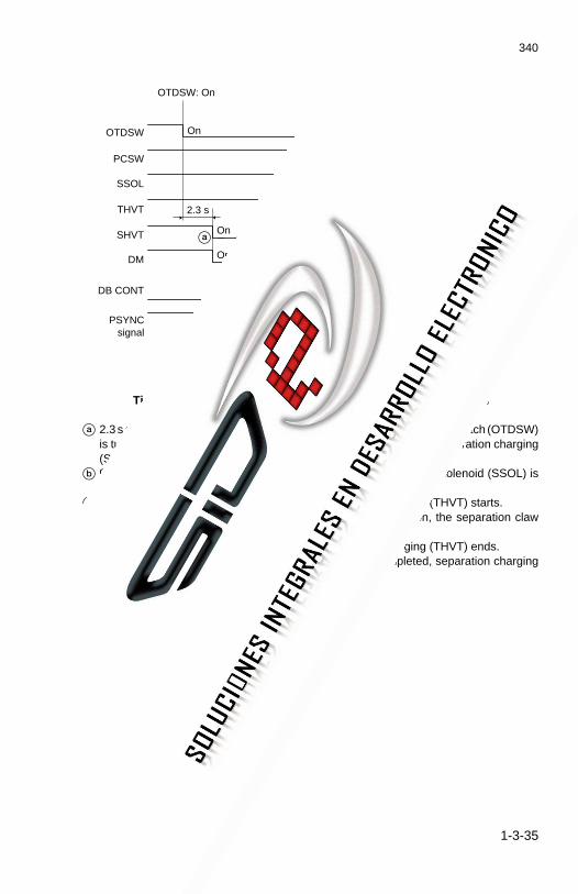
Timing chart 1-3-5 Operation of the main high-voltage transformer
a When the original is inserted, the original trailing edge detection switch (OTDSW) isturned on. After 2.3 s, the drive motor (DM) and drum motor (DRM) are turned on.
b 3.534 s (1 turn of the drum) after the drive motor (DM) and drum motor (DRM) are turnedon, the main high-voltage transformer (MHVT) is turned on to start main charging. Thegrid voltage (GRID CONT) and developing bias voltage (DB CONT) are controlledstepwise to increase the drum potential gradually.
c The drum potential reaches 870 V DC and the developing bias voltage (DB CONT) step-up control ends. After 3.534 s (1 turn of the drum), potential buildup is completed.
d 3 s after copying is completed and the eject switch (ESW) is turned off, the grid voltage(GRID CONT) and developing bias voltage (DB CONT) are controlled stepwise todecrease the drum potential gradually.
e When the grid voltage (GRID CONT) step-down control ends, the main high-voltagetransformer (MHVT) is turned off and main charging ends.
DMDRM
OTDSW
ESW
MHVT
GRID CONT
DB CONT
OTDSW: On ESW: OnESW: Off
OnOff
Off
Off
OffOnOn
2.3 sOn
3.534 s
3.534 s
3 s
1.6 s
400 ms
400 ms
600 ms
400 ms
400 ms
a
b
c
e
d
Potential buildup completed.

340-3
1-3-18
Drum surface potential correction
The grid control voltage (GRID CONT) is determined based on the target value set bysimulation 35 to maintain the drum surface potential around the developing section to870 V DC.
• Correction timings1) When any of the safety switches are turned off and on.2) When the power plug is removed and reinserted.3) When the main switch is turned off and on.
• Drum surface potential correction flow chart
Start.
End.
The grid voltage is controlled stepwise to increase the drum surface potential gradually.
V1: Drum potential sensor output value set by simulation 35 for the drum surface potential of 870 V DC. V2: Average of sampled drum potential sensor output values V3: Average of sampled drum potential sensor output values
Dark potential is stabilized (maximum data is reached).
Yes
Yes
No No
Yes Yes
No
No
V1 – 16 ≤ V2 < V1 V1 < V3 ≤ V1 + 16
V1 – 16 ≤ V3 < V1 V1 < V2 ≤ V1 + 16
Is this the 10th correction?
V1 – 4 ≤ V2, V3 ≤ V1 + 4
The drum potential sensor output is sampled 20 times and average value V2 is calculated.
The drum potential sensor output is sampled 20 times and average value V3 is calculated.
The grid control voltage (GRID CONT) is determined based on V1, V2 and V3.
C-551 “Dark potential correction problem” is triggered.
After 3.534 s (1 turn of the drum)
After 200 ms

340
1-3-19
(3) Exposure and original feed section
Figure 1-3-15 Exposure and original feed section
Exposure is accomplished by scan exposure method with a moving original. A fluorescentlamp is used as the light source. While being conveyed across the contact glass by therollers, the original is exposed by the fluorescent light and the exposed image is read by theCIS (contact image sensor).The fluorescent lamp heater (FLH) is installed on the fluorescent lamp (FL) to improve thetemperature characteristics which maintains the temperature of the fluorescent lamp toapproximately 40°C/104°F. The CIS reads the reflection of the fluorescent lamp (FL) lighton the middle upper original roller (white reference) to maintain the intensity constant.The original is fed by the rotation of the front/middle/rear upper original rollers and the front/rear lower original rollers. These rollers are controlled by the original leading edge detectionswitch (OLDSW), the original trailing edge detection switch (OTDSW), and the original feedclutch (OFCL). The original feed motor (OFM) drives the exposure section.
1 Original insertion guide2 Front upper original roller3 Middle upper original roller4 Contact glass5 Original holder rear guide6 Rear upper original roller7 Original feed rear guide8 Rear lower original roller
9 Original feed rear light shielding plate0 Fluorescent lamp (FL)! Fluorescent lamp heater (FLH)@ Front lower original roller# Original feed front light shielding plate$ Original feed front guide% SLA (SELFOC lens array)^ CIS (contact image sensor)
1
$
45 236
7
89
0!
#@% ^

340
1-3-20
Figure 1-3-16 Block diagram of the exposure and original feed section
CN2-14CN3-12
CN7-22CN6-18
CN4-13B
CN4-7ACN3-13
CN3-30
CN3-31
CN3-32
CN3-33
CN3-23
CN3-24
CN3-25
CN2-1CN2-10
CN2-11
CN2-12
CN2-13
CN2-2
CN2-3
a
b
c
abc
FLH REM
FL CONT
MPCB
FL REM
CN6-6
CN5-5
OPPCB
INPCB
DCM2PCB
OFM
CN
2-1
CN
2-6CN
1-1C
N1-2
FLH
RE
M
~
OT
DS
W
FLH
FLTH
OLD
SW
OF
CL
OFM SPEED1
OFM ENA
OFM SPEED2
e
fg
d
efg
d DCM2PCB TXD/RXD
DCM2PCB RXD/TXD
GS
GS
FL

340
1-3-21
Timing chart 1-3-6 Operation of the exposure and original feed section
a 640 ms after the original is inserted and the original leading edge detection switch(OLDSW) is turned on, the original feed motor (OFM) starts to rotate forward and theoriginal feed clutch (OFCL) is turned on to start conveying the original.
b After the original is conveyed and the original trailing edge detection switch (OTDSW)is turned on, the original feed clutch (OFCL) is turned off and the original stops at the copyready position.
c 1 s after the original trailing edge detection switch (OTDSW) is turned on, the CIS(contact image sensor) starts shading correction and the fluorescent lamp (FL) lights.
d As soon as the secondary paper feed starts, the original feed clutch (OFCL) is turned onand the original is conveyed across the contact glass for exposure.
e 500 ms after original exposure is completed and the original trailing edge detectionswitch (OTDSW) is turned off, the original feed motor (OFM) is turned off.
f 200 ms after the original feed motor (OFM) is turned off, it starts to rotate in reverse toreturn the original.
g When the original trailing edge detection switch (OTDSW) is turned off, the original feedclutch (OFCL) is turned off and, after 48 ms, the original feed motor (OFM) is turned offto complete original return operation.
h 500 ms after original return operation is completed, the original feed motor (OFM) startsto rotate forward for the exposure for the second copy, and the original feed clutch(OFCL) is turned on to convey the original.
i When the original is conveyed and the original trailing edge detection switch (OTDSW)is turned on, the original feed clutch (OFCL) is turned off and the original stops at the copyready position.
j As soon as the secondary feed of the second sheet starts, the original feed clutch (OFCL)is turned on and the original is conveyed across the contact glass for exposure for thesecond copy. The original feed motor (OFM) and original feed clutch (OFCL) then repeate to g to return the original.
k 1325 ms after original exposure is completed and the original trailing edge detectionswitch (OTDSW) is turned off, the fluorescent lamp (FL) is turned off.
FL
OLDSW
OTDSW
OFCL
OLDSW: On
OTDSW: On
OFM
OTDSW: Off OTDSW: Off OTDSW: Off OTDSW: Off
OTDSW: On
OnOn
On
On On
1 s
640 ms
500 ms200 ms
On On
On
On
On
Off 200 msOff
Off Off
Off Off
Off
Off
1325 ms
Off
500 ms 500 ms48 ms 48 ms
a
b
c
d
e e'f f'
g g
h
ij
k
'
Forward Stop
Reverse
Shading correction start
Secondary paper feed start
Second sheet secondary feed start
Roll unit paper feed, multiple copying (2 sheets).

340
1-3-22
(4) CIS and LPH sectionIn the CIS and LPH section, the CIS reads the original image exposed by the fluorescentlamp (FL) and the drum surface is irradiated by the LPH to form a static latent image on it.
Figure 1-3-17 CIS and LPH section
1 SLA (SELFOC lens array)2 LPH (LED printhead)
1 23
4
3 Fluorescent lamp (FL)4 CIS (contact image sensor)
Contains 1 and 3.

340-1
1-3-23
Figure 1-3-18 Block diagram of the CIS and LPH section
CN11
CN7-22CN6-18
CN17
CN22
CN21
FL CONTFL REM
INPCB CN
2-1
CN
2-6CN
1-1C
N1-2
~
FLCIS
LPH
ISUPCB
LPHROMPCB
LPHPSPCB5 V DC
GND MPCB

340-1
1-3-24
Original image reading
The CIS (contact image sensor) consists of four channels of 3712 phototransistors. Theoriginal image is read by 14592 phototransistors along a line of the width of A0 (934 mm),and its analog data is sent to the ISU PCB (ISUPCB).
Figure 1-3-19 Original image reading
Static latent image formation
The LPH (LED printhead) consists of 14592 LEDs which are turned on and off based on theimage data read by the CIS to form a static latent image on the drum surface line by line.Toner adheres only to the areas irradiated by the lit LEDs, so the image is formed.
Figure 1-3-20 Static latent image formation
1, 2, 3 14592
Channel 1
Original image
Channel 2
Channel 3
Channel 4
CIS (contact image sensor)
1 line
Phototransistors
SLA (SELFOC lens array)
1,2,3 14592
LED
1 line
LPH (LED printhead)
DrumSLA (SELFOC lens array)

340
1-3-25
Timing chart 1-3-7 Image reading and formation
a 1 s after the original is conveyed and the original trailing edge detection switch (OTDSW)is turned on, the CIS (contact image sensor) starts shading correction and thefluorescent lamp (FL) lights.
b The original feed clutch (OFCL) is turned on to start secondary original feed. At the sametime, the fluorescent lamp (FL) starts exposure and the CIS starts to read the originalimage.
c 450 ms after the original feed clutch (OFCL) is turned on, the OSYNC and PSYNCsignals are turned on and, in synch with these signals, the original image is processedand the LPH forms a static latent image, respectively.OSYNC signal: original leading edge synchronization signalPSYNC signal: image formation synchronization signal
d 450 ms after the original trailing edge detection switch (OTDSW) is turned off, theOSYNC and PSYNC signals are turned off to end image reading and formation.
e 1325 ms after original exposure ends and the original trailing edge detection switch(OTDSW) is turned off, the original feed motor (OFM) and original feed clutch (OFCL)are turned off. At the same time, the fluorescent lamp (FL) is turned off.
FL
OLDSW
OTDSW
OFCL
OSYNC signal
PSYNC signal
OLDSW: On
OFM
OTDSW: Off
OTDSW: On
OnOn
On
On On
Forward Stop
Reverse
1 s
450 ms 450 ms
640 ms
Off
Off
Off
1325 ms
Off
Shading correction start
Original and paper secondary feed start Image reading start
a
b
c d
e

340
1-3-26
CIS correction
• Shading correctionShading correction is carried out to correct the fluctuation in the fluorescent lamp (FL)intensity and variations in the sensitivity between the sensor elements constituting the CIS.If shading correction does not end within 30 s from its start, an original jam (J-05) isindicated. If shading correction fails to end six times successively after the original isreinserted, service call code C-300 is triggered.
Start.
End.
CIS black reference value is created (black shading).
Yes
Yes
No Is the average read-in value below A0H?
With the fluorescent lamp off, the average of the sensor read-in data is calculated for each channel.
CIS white reference value is created (white shading).
NoIs the average read-in value above 80H?
With the fluorescent lamp lit, the aver- age of the sensor read-in data on the middle upper original roller (white reference) is calculated for each channel (see Figure 1-3-21).
The CIS read-in data is corrected based on the black and white reference values while the original image is read in.
CIS
SLA
Fluorescent lamp (FL)
Middle upper original roller (white reference)
Figure 1-3-21 White shading

340
1-3-27
• AGC processing (gray level correction)The tone of the image is reproduced by dividing the CIS image read-in value into 256 levels.If the absolute white level is assumed to be 5.0 V and the absolute black level 0 V, the rangeof the actual image read-in value is narrower than the range from 0 to 5.0 V, so the tone ofthe reproduced image is affected. AGC processing (auto gain control) corrects the imageread-in value to reproduce gray levels more accurately.
Figure 1-3-22 AGC processing
Example: If the maximum white reference value (AGCHMAX) read by the CIS is 4.0 V andthe minimum black reference value (AGCLMIN) is 0.8 V, the range of the imageread-in value is narrower than the range between the absolute white level (5.0V) and absolute black level (0 V). In such a case, the read-in value cannot bedivided into 256 levels and the tone of the reproduced image is affected. AGCprocess corrects VREFH to 4.0 V, VREFL to 0.8 V and the correction value to 0so that the read-in value can be divided into 256 levels to reproduce the tone ofthe image more correctly.
• γ (gamma) correctionThere are slight differences in the black-level read-in values between the four channels ofthe CIS. Gamma correction can be made by executing simulation 120 so that an even imageoutput level is obtained.
Absolute white level (5.0 V)
Absolute black level (0 V)
AGCHMAX (4.0 V)
AGCLMIN (0.8 V)
VREFH (4.0 V + correction value)
VREFL (0.8 V + correction value) Before AGC processing
After AGC processing
Divided into 256 levels.

340-1
1-3-28
(5) Developing sectionThe developing section is comprised of the developing unit assembly and the toner hopperassembly. The developing unit assembly is comprised of the developing roller and doctorblade which form a magnetic brush, and the developer paddle and developer spiral rollerwhich mix the developer. The toner hopper assembly is installed on the top of the developingunit assembly to supply toner to the developing unit assembly and is comprised of the tonerfeed roller and the toner agitation rod.
Figure 1-3-23 Developing section
1 Developing roller2 Doctor blade3 Developing unit thermistor (DTH)4 Toner sensor (TNS)5 Upper developing unit stay6 Front hopper stay7 Developing unit partition
5
@
!
49
0
8 7 6
$#
2
1
3
8 Toner feed roller9 Toner agitation rod0 Hopper lid! Rear hopper stay@ Developing unit housing# Developer spiral roller$ Developer paddle
DBHVT
MPCB
CN2-18
CN2-2
CN4-3BCN4-4BCN2-19
CN4-1A
CN4-2A
345
TNS
DTH
DB REM
DB CHG
DB CONT
TM
Figure 1-3-24 Block diagram of the developing section

340-1
1-3-29
Forming the magnetic brush
The developer flows by the rotation of the developing roller and the magnetic brush is formedon pole N1. The height of the magnetic brush is set by the gap between the doctor bladeand the developing roller. The developing bias voltage (650 V DC) which is output from thedeveloping bias high-voltage transformer (DBHVT) is applied to the developing roller toimprove the image contrast. When the drum surface potential reaches 0 V after completionof copying, the developing bias voltage is switched to –100 V DC to prevent toner and carrierfrom adhering to the drum.
Figure 1-3-25 Forming the magnetic brush and agitation of the developer
A (gap between doctor blade and developing roller):0.55 to 0.65 mm around the center0.7 to 0.75 mm at both ends
N1: 900 × 10–4 ± 70 × 10–4TN2: 600 × 10–4 ± 60 × 10–4TS1: 750 × 10–4 ± 70 × 10–4TS2: 750 × 10–4 ± 70 × 10–4TS3: 600 × 10–4 ± 60 × 10–4T
1 Developing roller2 Doctor blade3 Developing unit partition4 Toner feed roller
A
S3
S1
S2
N2
N1
80°
60°
85°75°
60°
1
2
345
6
7
5 Toner agitation rod6 Developer spiral roller7 Developer paddle

340
1-3-30
Temperature compensation of the toner sensor output
Temperature compensation of the toner sensor (TNS) output value is applied by thefollowing formula.The output values from the toner sensor (TNS) and the developing unit thermistor (DTH)are input to the main PCB (MPCB). The main PCB samples the two input values at 8 msintervals. If two of three successive sampled input values are the same, this value is usedas one input value.
X = TS – K (TH – D26)where X: control input (V, toner sensor output value after temperature compensation)
TS: actual toner sensor output (V)K: temperature compensation coefficient (0.005 V/deg: TH > 26°C/79°F,
0.014 V/deg: TH < 26°C/79°F)TH: temperature of the developing unit (°C/°F, detected temperature of the
developing unit thermistor)D26: reference temperature (26°C/79°F)
A change in temperature TH – D26 based on the reference temperature (26°C/79°F) ismultiplied by temperature compensation coefficient K to obtain the temperature compensationvalue; this is then subtracted from actual toner sensor output TS. Because the rate ofincrease in the toner sensor output value is high when the temperature of the developingunit is greater than 26°C/79°F, the main PCB compensates the toner sensor outputfollowing the above formula, so as to lower the output. Because the rate of decrease in thetoner sensor output value is high when the temperature of the developing unit is less than26°C/79°F, the main PCB compensates to increase the output.

340
1-3-31
Toner sensor output correction based on the copy count
The toner sensor (TNS) output is corrected by the following formula based on the copy count(copy distance).
X = KM + TSwhere X: control input value (V, toner sensor output value after copy count correction)
M: copy distance after execution of simulation 60 (m)TS: actual toner sensor output (V)
K: distance correction coefficient (0.00021 V/m)
Figure 1-3-26
A The copy distance count is cleared during developer setting (simulation 60).B Until the copy distance reaches 1000 m, the actual toner sensor output value is corrected
by the formula as the copy distance increases.C When the copy distance exceeds 1000 m, the actual toner sensor output value is
corrected with a constant value of +0.21 V.
A
B
CControl input value (V)
Copy distance (m)
TS
10000
0.21 V

340
1-3-32
Toner density control
Figure 1-3-27 Toner density control
A The value set while simulation 60 (developer setting) is performed is used as the tonercontrol level (initial output value for the toner control sensor). Toner feed motor (TM) on/off control is based on this reference value.If the temperature- and count-corrected toner sensor output value exceeds the tonercontrol level, the toner feed motor is turned on for 0.5 s to supply toner from the tonerhopper to the developing unit assembly. (The toner feed motor can be turned on onlywhen the developing unit assembly is driven, i.e. the drive motor is on.)If the toner sensor output value does not drop during this 0.5 s period, the toner feedmotor is turned on for another 0.5 s, and this operation is repeated until the toner sensoroutput value becomes lower than the toner control level.
B If the toner sensor output value rises further and remains 0.234 V or more above the tonercontrol level for 10 s, the toner empty level is detected and toner feed aging operationis carried out. When the toner sensor output value reaches the toner control level, agingis performed for 3 minutes after toner replenishing ends (toner feed motor off). If thetoner sensor output value does not reach the toner control level after 3 minutes of tonerfeed aging, toner empty condition is detected and the add toner indicator on theoperation panel lights.
C When the toner sensor output value is 0.351 V or more above the toner empty level, thetoner empty high level is detected and the message requesting toner to be replenishedis shown on the display, inhibiting copying.
D When toner is replenished to the toner hopper and the toner sensor output value reachesthe toner control level, aging is performed for 3 minutes and then copying is enabled.
0.351 V
0.234 V
A B C D
3 minToner sensor output voltage (V)
Toner empty high level
Toner empty level
Toner control level
Add toner indictor on
Message requesting toner to be replenished
340
1-3-33
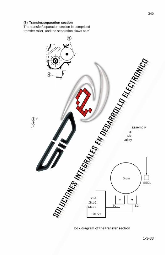
(6) Transfer/separation sectionThe transfer/separation section is comprised of the transfer charger assembly, the pre-transfer roller, and the separation claws as shown in Figure 1-3-28.
Figure 1-3-28 Transfer/separation section
1 Separation claw solenoid (SSOL)2 Tungsten wires3 Pre-transfer upper inner guide4 Pre-transfer pulley5 Pre-transfer outer guide6 Pre-transfer roller
Figure 1-3-29 Block diagram of the transfer section
87
1
3 2
4
@!0
9
65
7 Transfer charger8 Separation charger9 Transfer charger assembly0 Separation claws! Separation guide@ Separation pulley
CN4-1B
CN6-6
CN4-2BCN3-3
TC REM
ST ALARM
SC REM
MPCB
STHVT
SSOL
TC SC
CN1-1
CN1-2
CN1-3
Drum

340
1-3-34
The transfer charger assembly is divided into the transfer charger which transfers the tonerimage formed on the drum to the paper, and the separation charger which removes thepaper from the drum. Transfer charging and separation charging are performed by applyinghigh voltage which is output from the ST high-voltage transformer (STHVT) to both ends ofeach tungsten transfer charger and separation charger wires. The separation claws areinstalled to ensure paper separation.
Figure 1-3-30 Transfer charger assembly
1 Left transfer charger lid2 Left transfer seal3 Charger spring4 Transfer charger left housing5 Tungsten wire (for transfer
and separation charger)6 Right transfer charger lid
1
23
4
56
7
89
0!
@
#
7 Right transfer seal8 Screw9 Washer0 Transfer charger right housing! Transfer inner shield@ Transfer outer shield# Transfer wire
340
1-3-35
Timing chart 1-3-8 Operation of the transfer/separation section
a 2.3 s after the original is inserted and the original trailing edge detection switch (OTDSW)is turned on, the drive motor (DM) turns on and, at the same time, separation charging(SHVT) starts.
b 994 ms after the PSYNC signal is turned on, the separation claw solenoid (SSOL) isturned on.
c 1704 ms after the PSYNC signal is turned on, transfer charging (THVT) starts.d The moment the paper conveying switch (PCSW) is turned on, the separation claw
solenoid (SSOL) is turned off.e 1680 ms after the PSYNC signal is turned off, transfer charging (THVT) ends.f 800 ms after the developing bias step-down cotrol is completed, separation charging
(SHVT) ends.
OTDSW
OTDSW: OnOTDSW: Off
PCSW: On PCSW: Off
PCSW
SSOL
THVT
SHVT
DB CONT
On
2.3 s
944 ms
1704 ms 1680 ms
800 ms
Off
Off
Off
Off
On
On
DM OffOn
a
b
c e
f
dOn
Off
On
450 ms450 ms
Potential buildup completed. Primary original feed completed. Shading correction completed.
PSYNC signal

340-1
1-3-36
(7) Cleaning sectionCleaning is performed by the blade cleaning method and the cleaning fur brush. Thecleaning section is comprised of the cleaning blade and the cleaning fur brush which removethe residual toner adhering to the drum after transfer, and the cleaning unit spiral whichcollects and sends toner to the waste toner tank.The cleaning fur brush rotates always in contact with the drum surface and prevents thetoner scraped off the drum by the cleaning blade from dropping inside of the machine. Otherforeign matter such as paper fragments adhering to the surface of the drum are alsoremoved by the brush.When the waste toner tank becomes full, the overflow sensor (OFS) is turned off and amessage requesting the waste toner tank to be checked appears on the display on theoperation panel, and copying is inhibited.
Figure 1-3-31 Cleaning section
5
21
76
3
4
1 Cleaning blade2 Cleaning unit cover3 Cleaning housing4 Cleaning fur brush
5 Cleaning solenoid (CSOL)6 Cleaning unit spiral7 Lower cleaning blade

340
1-3-37
Figure 1-3-32 Block diagram of the cleaning section
OFS
MPCB
CN6-5
CN6-4
CN3-8
CSOL
CSOL 1
CSOL 2
TDT DSW
CN3-7

340
1-3-38
Timing chart 1-3-9 Operation of the cleaning solenoid
The cleaning solenoid (CSOL) is controlled by signals CSOL 1 and CSOL 2.
a 1.3 s after the original is inserted and the original trailing edge detection switch (OTDSW)is turned on, signals CSOL 1 and CSOL 2 are turned on and the cleaning solenoid(CSOL) is turned on.
b 1 s after the cleaning solenoid (CSOL) is turned on, the CSOL 1 signal is turned off. Thecleaning solenoid (CSOL) stays on.
c 10 minutes after copying is completed and the drive motor (DM) is turned off, the CSOL2 signal is turned off and the cleaning solenoid (CSOL) is turned off. (If the drive motoris turned back on for the next copy cycle within 10 minutes after it was turned off, a isrepeated.)
d 1 s after the cleaning solenoid (CSOL) is turned off, the CSOL 1 and CSOL 2 signals areturned on and off at intervals of 1 s and the cleaning solenoid (CSOL) is turned on twice.
1 s
1.3 s
10 min
DM
OTDSW
CSOL 1
CSOL 2Off
Off
On On
On
OnOff
OTDSW: On OTDSW: Off
On
On1 s 1 s
1 s
1 s 1 s
On On
ab
c d
Off
Off

340
1-3-39
(8) Static eliminator sectionThe static eliminator section is comprised of the two cleaning lamps as shown in Figure1-3-33. The post-transfer lamp (RTL) is to eliminate unnecessary charge, and the pre-charging lamp (PCHL) is to eliminate the residual charge after transfer.
Post-transfer lamp ....... Since the transfer charger has been turned on before the latentstatic image on the drum reaches the transfer charger, this lampeliminates the unnecessary charge generated by the transfercharger and prepares for the next main charging (copy operation).
Pre-charging lamp ....... Eliminates the residual charge on the drum after the toner isremoved in the cleaning section to prepare for the next copy.
Figure 1-3-33 Static eliminator section
Pre-charging lamp (PCHL)
Post-transfer lamp (RTL)

340
1-3-40
Figure 1-3-34 Block diagram of the static eliminator section
CN6-8
CN5-6
CN5-7
CN6-7
OPPCBCN4-12B
CN4-12A
RTL REM
PCHL REM
MPCB
PCHL
RTL
Drum
Timing chart 1-3-10 Operation of the static eliminator section
a After the drive motor (DM) is turned on, the pre-charging lamp (PCHL) and the post-transfer lamp (RTL) are turned on.
b After copying operation, the drive motor (DM) is turned off. Then the pre-charging lamp(PCHL) and the post-transfer lamp (RTL) are turned off.
2.3 sOTDSW
DM
PCHL
RTL
On
On
On
OnOff
Off
Off
Off
OTDSW: On OTDSW: Off
a b

340
1-3-41
(9) Fixing section
Figure 1-3-35 Fixing section
(
21567
98
&*
^%$# 4@
!
0
3
› ‹¤
)⁄
1 Fixing heater M (H1)2 Fixing heater S (H2)3 Oil roller4 Heat roller5 Fixing unit thermal switch 1 (FTSW1)6 Fixing unit thermal switch 2 (FTSW2)7 Fixing unit upper partition8 Fixing unit thermistor 1 (FTH1: near
the center of the heat roller)9 Fixing unit thermistor 2 (FTH2: right
end of the heat roller)0 Fixing unit cover! Fixing unit middle front guide@ Separation pulleys
# Fixing unit front guide$ Fixing unit lower partition% Front lower removal cover^ Press roller& Fixing unit thermistor 3 (FTH3: near
the center of the press roller)* Fixing unit thermistor 4 (FTH4: right
end of the press roller)( Lower eject guide) Press roller separation claw⁄ Eject roller¤ Eject pulley‹ Upper eject guide› Separation claw

340-3
1-3-42
The fixing section is comprised of the parts shown in Figure 1-3-35. After the transferoperation, the paper is conveyed to the fixing section and passes between the heat rollerand the press roller. A constant pressure is applied between the heat roller and the pressroller by the fixing press spring and the toner transferred is fixed on the paper by the heatand pressure applied from each roller.Fixing heater M (H1) heats the center of the heat roller and fixing heater S (H2) heats theends of the heat roller.The oil roller cleans the surface of the heat roller to prevent the paper from wrapping aroundthe heat roller.After fixing, the paper is separated from the heat roller by the separation claws and ejectedto outside of the machine via the eject roller and the eject pulley.
Figure 1-3-36 Block diagram of the fixing section
CN4-8BCN4-7BCN4-3A
SSR2 REMSSR1 REMSSR3 REM
MPCB
CN2-5
FDM CLKCN3-4
CN7-6CN7-7
FDM REMCN3-3
DCM1PCB
CN5-1CN5-2CN5-3CN5-4
PRY1 FTSW1
FTSW2
FR*H2H1
+−FGFG
FTH1
CN2-6 FTH2
CN2-7 FTH3
CN2-8 FTH4
CN2-10 ETTH
CN3-16 ESW
CN3-17
CN4-5ACN4-5B
FPS
FFM-R
FFM-L
FFM REM
FFM H/L
*For 230 V, 50 Hz models only.
FDM
SSR2 SSR1
SSR3*

340
1-3-43
Heating and temperature control of heat roller and press roller
• Heat roller temperature control 1Fixing unit thermistor 1 (FTH1) detects the surface temperature around the center of theheat roller and fixing unit thermistor 2 (FTH2) detects the surface temperature of the rightend of the heat roller.If the temperature TPRD (surface temperature around the center of the press roller) detectedby fixing unit thermistor 3 (FTH3) becomes less than TPTH, fixing heaters M and S (H1 andH2) are turned on to heat the heat roller. Control temperature T is controlled by the followingformula.
Control temperature T = THCON + k (TPTH – TPRD)When (TPTH – TPRD) < 0, T = THCON.
THCON: heat roller control temperaturek: temperature compensation coefficient (standby: 0.33, copying: 1)
TPTH: press roller temperature threshold valueTPRD: fixing unit thermistor 3 (FTH3) temperature (surface temperature around
the center of the press roller)
Figure 1-3-37 Fixing temperature control
Standby StandbyCopy start
Copy end
THCON
TPTH
90˚C/194˚F 80˚C/176˚F
Heat roller temperature
Heat roller control temperature
Press roller surface temperature

340
1-3-44
• Heat roller temperature control 2When the temperature TETTH detected by the external temperature thermistor (ETTH) is asin the table, the control temperatures are changed to prevent poor fixing. If the ambienttemperature is below 15°C/59°F, fixing is not performed sufficiently, and if greater than30°C/86°F, the image may be blurred.
The heat roller control temperature and the press roller temperature threshold value mustbe changed as follows depending on the paper used (plain paper, tracing paper, or film) toprevent poor fixing.
External temperature thermistordetection temperature
Primary stabilizationtemperature
Secondary stabilizationtemperature
TETTH ≤ 15°C/59°F 145°C/293°F 165°C/329°F
15°C/59°F < TETTH < 30°C/86°F 165°C/329°F 155°C/311°F
30°C/86°F ≤ TETTH 165°C/329°F 155°C/311°F
External tempera-ture thermistor
detectiontemperature
Heat roller controltemperature
Press roller temperaturethreshold value
TETTH ≤ 15°C/59°F 155°C/311°F
15°C/59°F < TETTH
< 30°C/86°F
30°C/86°F ≤ TETTH
Plainpaper
Tracingpaper
Film Plainpaper
Tracingpaper
Film
150°C/302°F
155°C/311°F
105°C/221°F
100°C/212°F
105°C/221°F
150°C/302°F
145°C/293°F
150°C/302°F
145°C/293°F
140°C/284°F
145°C/293°F
105°C/221°F
100°C/212°F
105°C/221°F
105°C/221°F
100°C/212°F
105°C/221°F

340
1-3-45
• Press roller temperature control 1If the surface temperature of the press roller is less than its minimum value or the surfacetemperature between the heat roller side and on the opposite side is different, fixingproblems may occur. Therefore, the following control is performed to keep the surfacetemperature of the press roller constant.In ready status, if the fixing unit thermistor 3 (FTH3) temperature (temperature around thecenter of the press roller) becomes less than 80°C/176°F, fixing heaters M and S (H1 andH2) are turned on. The fixing drive motor (FDM) is then turned on at low speed to increasethe surface temperature of the press roller. When the temperature of fixing unit thermistor3 (FTH3) reaches 90°C/194°F, fixing heaters M and S (H1 and H2) and the fixing drive motor(FDM) are turned off. By repeating these operations, the surface temperature of the pressroller is maintained between 80°C/176°F and 90°C/194°F.
• Press roller temperature control 2When copies are made with small-size paper, the press roller temperature becomes higherat the ends where no paper passes than around the center where paper passes. Thiscauses the ends of the press roller to swell, reducing the paper conveying force around thecenter.After copying is completed, the fixing unit thermistor 3 (FTH3) temperature (temperaturearound the center of the press roller) is compared to the fixing unit thermistor 4 (FTH4)temperature (temperature at the right end of the press roller), and the fixing drive motor(FDM) speed is corrected in proportion to the temperature difference to prevent the paperconveying speed from decreasing in the fixing unit.
Figure 1-3-38 Heat roller and press roller temperature detection
Fixing heater M
Fixing heater S
Fixing unit thermistor 1
Fixing unit thermistor 3
Fixing unit thermistor 2
Fixing unit thermistor 4
Heat roller
Press roller

Xi3648 (MCA) S/M
ELECTRICALSECTION
II
II El
ectri
cal S
ectio
n

1-1-11
340
CONTENTS
2-1 Electrical Parts Layout
2-1-1 Electrical parts layout .......................................................................... 2-1-1

340-3
2-1-1
2-1-1 Electrical parts layout
Figure 2-1-1 Printed circuit boards
8
11
152224
14
10
6
13
4
2
9 1
3
516
21 1819
7
12
17
20
Machine left Machine inside Machine right
Right frame Left frame
Machine rear
23
1. Main PCB (MPCB) ............................................. Output control for imageprocessing and LED printhead(LPH) and control of otherelectrical components.
2. ISU PCB (ISUPCB) ............................................ Digital conversion of data fromthe contact image sensor (CIS)and data correction.

340-3
2-1-2
3. LPHROM PCB (LPHROMPCB) ......................... Stores LPH light intensitycorrection data.
4. Operation unit PCB (OPCB) .............................. Consists of operation keys,display LEDs and LCD.
5. Servo motor control 1 PCB (DCM1PCB) ........... Drive control of the drive motor,drum motor and fixing drive motor.
6. Servo motor control 2 PCB (DCM2PCB) ........... Drive control of the original feedmotor and paper feed motor.
7. Power source PCB (PSPCB) ............................. Output of 24 V, 5 V DC and±12 V DC supplies.
8. LPH power supply PCB (LPHPSPCB) ............... Converts 24 V DC into 5 V DCand supplies 5 V DC to LPH.
9. Output PCB (OPPCB)........................................ Powers roll unit heaters,dehumidifier, fluorescent lampheater, pre-charging lamp andpost-transfer lamp, and distributes24 V DC supply to multipledestinations.
10. Drum potential sensor PCB (DPSPCB) ............. Detection of input to the drumpotential sensor.
11. Inverter PCB (INPCB) ........................................ Output of DC supply to thefluorescent lamp.
12. Backup PCB (BUPCB) ....................................... Stores various setting data.13. Main high-voltage transformer (MHVT) ............. Generates a high voltage for main
charging.14. ST high-voltage transformer (STHVT) ............... Generates a high voltage for
transfer and separation charging.15. Developing bias high-voltage transformer
(DBHVT) ............................................................ Generates a developing biasvoltage.
16. Solid state relay 1 (SSR1) ................................. Turns power supply to fixingheater M on and off.
17. Solid state relay 2 (SSR2) ................................. Turns power supply to fixingheater S on and off.
18. Power relay 1 (PRY1) ........................................ Turns AC power supply on andoff.
19. Power relay 2 (PRY2) ........................................ Turns 24 V DC supply on and off.20. Power relay 3 (PRY3) ........................................ Turns 24 V DC supply on and off.21. Noise filter (NF) .................................................. Reduces noise on the power
supply line.22. Dehumidifier PCB (DRPCB) .............................. Supplies 24 V DC to the
dehumidifiers.23.* Flicker resistor (FR) ........................................... Regulates surge current flowing
into the fixing heater M.24.* Solid state relay 3 (SSR3) ................................. Short-circuits the flicker resistor.
*For 230 V, 50 Hz models only.

340-3
2-1-3
1. Main switch (MSW) ............................................ Turns AC power supply to thepower source PCB on and off.
2. Safety switch 1 (SSW1) ..................................... Forms a safety circuit when theleft front cover is open.
3. Safety switch 2 (SSW2) ..................................... Forms a safety circuit when theright front cover is open.
4. Safety switch 3 (SSW3) ..................................... Forms a safety circuit when theright cover is open.
5. Safety switch 4 (SSW4) ..................................... Forms a safety circuit when themain unit is open.
6. Safety switch 5 (SSW5) ..................................... Forms a safety circuit when themain unit is open.
7
8
5
12 1096
2,3
1
4
47
40
48
49
41
42
39
18,27,28
17,25,26
11
16,23,24
37,38
13,4335,36
30,3114
4534,44
Machine left Machine inside Machine right
21,22
2946
33
19
20
32 15
Figure 2-1-2 Switches and sensors (1)

340-3
2-1-4
7. Safety switch 6 (SSW6) ..................................... Forms a safety circuit when theupper rear cover is open.
8. Original holding section switch (OHSW) ............ Detects that the original holdingsection is open.
9. Bypass timing switch (BYPTIMSW) ................... Control of bypass registrationclutch.
10. Bypass registration switch (BYPRSW) .............. Detection of leading edge ofpaper from the bypass table,control of paper feed motor andbypass registration clutch, anddetection of paper jams in thebypass feed section.
7
8
5
12 1096
2,3
1
4
47
40
48
49
41
42
39
18,27,28
17,25,26
11
16,23,24
37,38
13,4335,36
30,3114
4534,44
Machine left Machine inside Machine right
21,22
2946
33
19
20
32 15
Figure 2-1-3 Switches and sensors (2)

340
2-1-5
11. Registration switch (RSW) ................................. Control of paper feed motor, drivemotor, fixing drive motor, feedclutch, roll paper conveying clutchand registration clutch anddetection of paper jams.
12. Paper conveying switch (PCSW) ....................... Control of separation clawsolenoid and detection of paperjams.
13. Eject switch (ESW) ............................................ Control of drive motor, fixing drivemotor and fixing unit fan motor,and detection of paper jams.
14. Original trailing edge detection switch(OTDSW) ........................................................... Detection of document passage
timing, control of drive motor,fixing drive motor, paper feedmotor, paper feed clutch, rollpaper conveying clutch,registration clutch, bypassregistration clutch and cutterclutch, and detection of originaljams.
15. Original leading edge detection switch(OLDSW) ........................................................... Detection of original insertion and
control of original feed motor andoriginal feed clutch.
16. Upper roll paper leading edge detectionswitch (RLDSW-U) ............................................. Detection of paper leading edge
home position, control of upperfeed clutch and upper roll windingclutch, and detection of paperjams.
17. Middle roll paper leading edge detectionswitch (RLDSW-M) ............................................ Detection of paper leading edge
home position, control of middlefeed clutch and middle rollwinding clutch, and detection ofpaper jams.
18. Lower roll paper leading edge detectionswitch (RLDSW-L)*1 .......................................................... Detection of paper leading edge
home position, control of lowerfeed clutch and lower roll windingclutch, and detection of paperjams.
19. Cutter home position switch 1 (CHPSW1) ......... Detection of cutter home position.20. Cutter home position switch 2 (CHPSW2) ......... Detection of cutter home position.21. Original size switch 1 (OSSW1) ......................... Detection of original size.22. Original size switch 2 (OSSW2) ......................... Detection of original size.
*1 Optional.

340-3
2-1-6
23. Upper paper size switch 1 (PSSW1-U) .............. Detection of paper size in the 1stroller unit.
24. Upper paper size switch 2 (PSSW2-U) .............. Detection of paper size in the 1stroller unit.
25. Middle paper size switch 1 (PSSW1-M) ............ Detection of paper size in the 2ndroller unit.
26. Middle paper size switch 2 (PSSW2-M) ............ Detection of paper size in the 2ndroller unit.
27. Lower paper size switch 1 (PSSW1-L)*1 ................. Detection of paper size in the 3rdroller unit.
7
8
5
12 1096
2,3
1
4
47
40
48
49
41
42
39
18,27,28
17,25,26
11
16,23,24
37,38
13,4335,36
30,3114
4534,44
Machine left Machine inside Machine right
21,22
2946
33
19
20
32 15
Figure 2-1-4 Switches and sensors (3)
*1 Optional.

340-3
2-1-7
28. Lower paper size switch 2 (PSSW2-L)*1 ................. Detection of paper size in the 3rdroller unit.
29. Waste toner tank detection switch(TDTDSW) ......................................................... Detects presence of the waste
toner tank.30. Fixing unit thermal switch 1 (FTSW1) ................ Forms the fixing heater M and S
safety circuits.31. Fixing unit thermal switch 2 (FTSW2) ................ Forms the fixing heater M and S
safety circuits.32. Fluorescent lamp thermistor (FLTH) .................. Detection of temperature in
vicinity of fluorescent lamp.33. Dehumidifier switch (DRSW) ............................. Turns AC power supply to the
dehumidifier PCB on and off.34. Developing unit thermistor (DTH) ...................... Detection of temperature in
vicinity of developing unit.35. Fixing unit thermistor 1 (FTH1) .......................... Detection of temperature of heat
roller at the center.36. Fixing unit thermistor 2 (FTH2) .......................... Detection of temperature of heat
roller at right end.37. Fixing unit thermistor 3 (FTH3) .......................... Detection of temperature of press
roller at the center.38. Fixing unit thermistor 4 (FTH4) .......................... Detection of temperature of press
roller at right end.39. External temperature thermistor (ETTH) ........... Detection of external (ambient)
temperature.40. Upper pulse sensor (PS-U) ................................ Detection of paper-out or paper
jam on 1st roller unit.41. Middle pulse sensor (PS-M) .............................. Detection of paper-out or paper
jam on 2nd roll unit.42. Lower pulse sensor (PS-L)*1 ......................................... Detection of paper-out or paper
jam on 3rd roller unit (option).43. Fixing unit pulse sensor (FPS) ........................... Detection of paper jam in fixing
unit.44. Toner sensor (TNS) ........................................... Detection of toner density in
developing unit.45. Drum potential sensor (DPS) ............................. Detection of drum surface
potential.46. Overflow sensor (OFS) ...................................... Detection of overflow of toner
collected in the waste toner tank.47. Upper roll heater switch (RHSW-U)*2 ....................... Upper roller unit heater in use/not
in use.48. Middle roll heater switch (RHSW-M)*2 ..................... Middle roll unit heater in use/not in
use.49. Lower roll heater switch (RHSW-L)*1 ........................ Lower roll unit heater in use/not in
use.
*1 Optional.*2 Optional for 220 – 240 V models.

340-1
2-1-8
3
1
4
11,12
2
8
5
6
7
9,10
Machine left Machine inside Machine right
Figure 2-1-5 Motors

340
2-1-9
1. Drive motor (DM) ............................................... Drives developing unit andtransfer unit.
2. Original feed motor (OFM) ................................. Drives original feed unit.3. Paper feed motor (PFM) .................................... Drives paper feed unit.4. Fixing drive motor (FDM) ................................... Drives fixing unit.5. Drum motor (DRM) ............................................ Drives the drum section.6. Toner feed motor (TM) ....................................... Supplies of toner.7. Paper conveying fan motor (PCFM) .................. Assistance of paper conveying,
and heat exhaust.8. Cooling fan motor (CFM) ................................... Heat exhaust from unit interior.9. LPH fan motor 1 (LPHFM1) ............................... Cools LED printhead (LPH).
10. LPH fan motor 2 (LPHFM2) ............................... Cools LED printhead (LPH).11. Right fixing unit fan motor (FFM-R) ................... Heat exhaust in fixing unit.12. Left fixing unit fan motor (FFM-L) ...................... Heat exhaust in fixing unit.

340-1
2-1-10
25
7
48 22
5
23
6
24
10
9
3
2
2719
2617
12,13
11
114,18 15
16
20,21
Machine left Machine inside Machine right
Figure 2-1-6 Others
1. Original feed clutch (OFCL) ............................... Original feed (control of originalfeed roller rotation).
2. Registration clutch (RCL) ................................... Secondary feed of paper fed fromroll unit (control of registrationroller rotation).
3. Roll paper conveying clutch (RPCCL) ............... Conveying paper fed from roll unit(rotation control of front roll paperconveying roller).
4. Upper roll winding clutch (RWCL-U) .................. Winding of paper roll (control of1st roll unit paper roll shaftrotation).

340
2-1-11
5. Middle roll winding clutch (RWCL-M)................. Winding of paper roll (control of2nd roll unit paper roll shaftrotation).
6. Lower roll winding clutch (RWCL-L)*1 ...................... Winding of paper roll (control of3rd roll unit paper roll shaftrotation).
7. Bypass registration clutch (BYPRCL) ................ Secondary paper feed duringmanual insertion (control ofbypass registration roller rotation).
8. Upper feed clutch (FCL-U) ................................. Primary paper roll feed from 1stroll unit (control of roll paper feedlower roller A rotation).
9. Middle feed clutch (FCL-M) ............................... Primary paper roll feed from 2ndroll unit (control of roll paperconveying rear roller B rotation).
10. Lower feed clutch (FCL-L)*1 .......................................... Primary paper feed from 3rd rollunit (option) (control of roll paperconveying rear roller B rotation).
11. Cutter clutch (CCL) ............................................ Cutter operation.12. Cleaning solenoid (CSOL) ................................. Cleaning blade operation.13. Separation claw solenoid (SSOL) ...................... Operation of separation claws.14. Fluorescent lamp (FL) ........................................ Exposues of original.15. Contact image sensor (CIS) .............................. Converts original data into analog
signal and outputs it.16. LED printhead (LPH) ......................................... Forms an image using the data
from the original on drum surfacevia LED illumination.
17. Ready lamp (R-Lamp) ....................................... Indicates that copying is possible.18. Fluorescent lamp heater (FLH) .......................... Maintains temperature of
fluorescent lamp.19. Dehumidifier (DH) .............................................. Prevents condensation on drum.20. Fixing heater M (H1) .......................................... Heats the center of the heat roller.21. Fixing heater S (H2) ........................................... Heats both ends of the heat roller.22. Upper roll unit heater (RH-U)*2 .................................... Dehumidifies paper in 1st roll unit.23. Middle roll unit heater (RH-M)*2 ................................... Dehumidifies paper in 2nd roll
unit.24. Lower roll unit heater (RH-L)*1 ..................................... Dehumidifies paper in 3rd roll unit
(optional).25. Total counter (TC) .............................................. Displays number of copies.26. Pre-charging lamp (PCHL) ................................ Improves evenness of charging
(main charging).27. Post-transfer lamp (RTL) ................................... Removes residual charge on
drum.
*1 Optional.*2 Optional for 220 – 240 V models.

1-1-13
340
CONTENTS
2-2 Detection of Paper Misfeed
2-2-1 Paper misfeed detection ..................................................................... 2-2-12-2-2 Paper misfeed detection conditions .................................................... 2-2-2

340
2-2-1
2-2-1 Paper misfeed detection
When a paper jam occurs, the copier immediately stops copying and the display on theoperation unit shows a code consisting of “J” followed by a number between 01 and 06,indicating the location of the jam.Paper jam counts sorted by the detecting conditions can be checked by simulation 74.To remove paper jammed in the copier, open the front covers and take out a roll unit, or openthe main unit, fixing unit, or original holding section.To reset the paper misfeed detection, open and close the front covers, main unit, right cover,upper rear cover or original holding section to turn safety switches 1 & 2, 4 & 5, 3, 6 or theoriginal holding section switch off and on, respectively.
Metric
Inch
J-01: paper feed section (1st roll unit)J-02: paper feed section (2nd roll unit)J-03: paper feed section (3rd roll unit*1)J-04: paper feed section (bypass paper feed section)J-05: original feed sectionJ-06: inside the copier main unit
*1 Optional.
Figure 2-2-1 Misfeed indication
PAPER MISFEED OPEN FRONT COVERS.
J-02
Paper jam Open front covers
J-02

340-1
2-2-2
2-2-2 Paper misfeed detection conditions
Figure 2-2-2 Misfeed detection
OLDSWOFCL
PCSW BYPRSW
BYPRCL
RCLRSW
FCL-M
FCL-L
OTDSW
ESW FPS
CCL
FCL-U

340
2-2-3
FCL-U
RSW 2720 ms
On
Off
On
Off
1. Paper jam in the paper feed section (1st roll unit): J-01When the new paper roll is wound up (first paper feed), the registration switch (RSW)does not turn on within 2720 ms after the upper feed clutch (FCL-U) has turned on.
Timing chart 2-2-1
When the paper roll need not be wound up (from the second sheet), the registrationswitch (RSW) does not turn on within 936 ms after the upper feed clutch (FCL-U) hasturned on.
Timing chart 2-2-2
2. Paper jam in the paper feed section (2nd roll unit): J-02When the new paper roll is wound up (first paper feed), the registration switch (RSW)does not turn on within 3632 ms after the middle feed clutch (FCL-M) has turned on.
Timing chart 2-2-3
When the paper roll need not be wound up (from the second sheet), the registrationswitch (RSW) does not turn on within 936 ms after the middle feed clutch (FCL-M) hasturned on.
Timing chart 2-2-4
FCL-U
RSW 936 ms
On
Off
On
Off
FCL-M
RSW 3632 ms
On
Off
On
Off
FCL-M
RSW 936 ms
On
Off
On
Off

340
2-2-4
3. Paper jam in the paper feed section (3rd roll unit): J-03When the new paper roll is wound up (first paper feed), the registration switch (RSW)does not turn on within 6380 ms after the lower feed clutch (FCL-L) has turned on.
Timing chart 2-2-5
When the paper roll need not be wound up (from the second sheet), the registrationswitch (RSW) does not turn on within 936 ms after the lower feed clutch (FCL-L) hasturned on.
Timing chart 2-2-6
4. Paper jam in the paper feed section (bypass paper feed section): J-04The bypass registration switch (BYPRSW) is on when the main switch (MSW) is turnedon or during ready mode.
FCL-L
RSW 6380 ms
On
Off
On
Off
FCL-L
RSW 936 ms
On
Off
On
Off
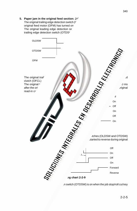
340
2-2-5
5. Paper jam in the original feed section: J-05The original trailing edge detection switch (OTDSW) does not turn on within 3 s after theoriginal feed motor (OFM) has turned on to start original feed.The original leading edge detection switch (OLDSW) stays off 1 s after the originaltrailing edge detection switch (OTDSW) has turned on.
Timing chart 2-2-7
The original trailing edge detection switch (OTDSW) stays off when the original feedclutch (OFCL) turns on during original read-in control.The original trailing edge detection switch (OTDSW) does not turn off within 3500 msafter the original leading edge detection switch (OLDSW) has turned off during originalread-in control.
Timing chart 2-2-8
The original leading edge and trailing edge detection switches (OLDSW and OTDSW)are off 2500 ms after the original feed motor (OFM) has started to reverse during originalread-in control.
Timing chart 2-2-9
The original trailing edge detection switch (OTDSW) is on when the job stop/roll cut keyis pressed.
OTDSW
OFM 640 ms
On
Off
On
Off
OLDSW
3 s
1 sOff
On
OTDSW
OFCL
3500 ms
On
Off
On
Off
OLDSW
Off
On
OTDSW
OFM
2500 ms
On
Off
Reverse
Forward
OLDSW
Off
On

340-1
2-2-6
6. Paper jam inside the copier main unit: J-06The registration switch (RSW), paper conveying switch (PCSW) or eject switch (ESW)is on when the main switch (MSW) is turned on or during ready mode.The paper conveying switch (PCSW) does not turn on within 3392 ms after theregistration clutch (RCL) has turned on.
Timing chart 2-2-10
The eject switch (ESW) does not turn on within 3752 ms after the paper conveying switch(PCSW) has turned on.
Timing chart 2-2-11
The registration switch (RSW) does not turn off within 2240 ms after the cutter clutch(CCL) has turned on.
Timing chart 2-2-12
RCL
PCSW 3392 ms
On
Off
On
Off
PCSW
ESW 3752 ms
On
Off
On
Off
CCL
RSW 2240 ms
On
Off
On
Off

340
2-2-7
The eject switch (ESW) does not turn off within 8s after the registration clutch (RCL) hasturned off.
Timing chart 2-2-13
No pulse signal is detected from the fixing unit pulse sensor (FPS) for 1 s while the ejectswitch (ESW) is on.
Timing chart 2-2-14
RCL
ESW 8 s
On
Off
On
Off
ESW
FPS
On
Off
On
Off
Pulse detection time

Xi3648 (MCA) S/M
III S
et U
p an
d
Adj
ustm
ent S
ectio
n
III
SET UP ANDADJUSTMENT
SECTION
1-1-15
340
CONTENTS
2-3 Operation of the PCBs
2-3-1 Power source PCB .............................................................................. 2-3-1(1) Noise filter circuit ......................................................................... 2-3-2(2) Rectification/surge limiter/smoothing circuit ................................ 2-3-2(3) Pulse width control circuit ............................................................ 2-3-3(4) 24 V DC output/error detection circuit ......................................... 2-3-4(5) 5 V DC output/5 V DC over-current protection circuit .................. 2-3-5(6) Over-voltage protection circuit ..................................................... 2-3-6
2-3-2 LPH power supply PCB ...................................................................... 2-3-7(1) Noise filter circuit ......................................................................... 2-3-7(2) Pulse width control circuit ............................................................ 2-3-8(3) 5 V DC output/error detection circuit ........................................... 2-3-9
2-3-3 Servo motor control 1 PCB ............................................................... 2-3-10(1) Drive motor control circuit .......................................................... 2-3-10(2) Fixing drive motor control circuit ................................................ 2-3-11(3) Drum motor control circuit ......................................................... 2-3-12
2-3-4 Servo motor control 2 PCB ............................................................... 2-3-13(1) Original feed motor control circuit .............................................. 2-3-14(2) Paper feed motor control circuit ................................................ 2-3-15(3) Reset circuit ............................................................................... 2-3-15
2-3-5 Main PCB .......................................................................................... 2-3-16(1) Fixing temperature error detection circuit .................................. 2-3-17(2) Reset circuit ............................................................................... 2-3-18(3) Image processing unit ............................................................... 2-3-20
2-3-6 Backup PCB ...................................................................................... 2-3-252-3-7 ISU PCB............................................................................................ 2-3-26
(1) Analog processing unit .............................................................. 2-3-27(2) A-D conversion/AGC processing unit ........................................ 2-3-28(3) Shading correction circuit .......................................................... 2-3-28
2-3-8 Operation unit PCB ........................................................................... 2-3-292-3-9 Inverter PCB ..................................................................................... 2-3-30
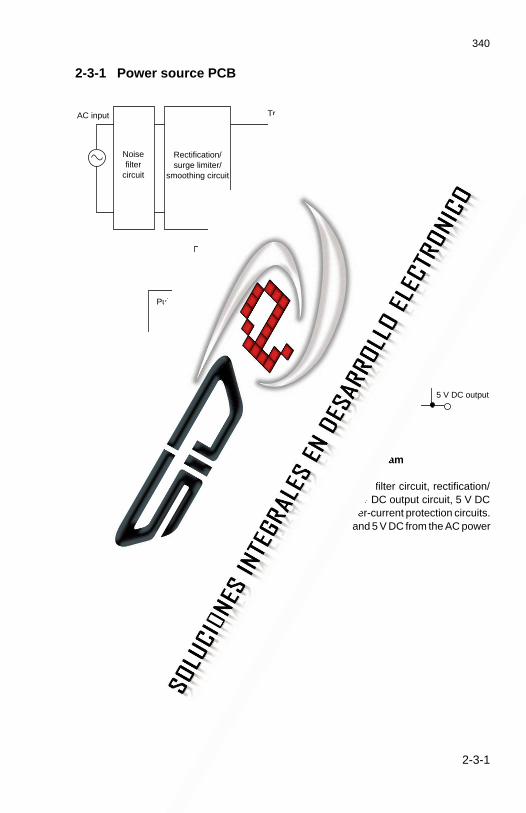
340
2-3-1
2-3-1 Power source PCB
Noise filter
circuit
Rectification/ surge limiter/
smoothing circuit
FET
Photocoupler
Photocoupler
Pulse width control/ over-current
protection circuit
24 V DC output circuit
Over-voltage detection circuit
Error detection circuit
AC input Transformer
24 V DC output
5 V DC output circuit
GND
GND
+12 V DC
–12 V DC
5 V DC output
±12 V DC output circuit
Figure 2-3-1 Power source PCB block diagram
The main components of the power source PCB are the noise filter circuit, rectification/surge limiter/smoothing circuit, pulse width control circuit, 24 V DC output circuit, 5 V DCoutput circuit, ±12 V DC output circuit and over-voltage and over-current protection circuits.The power source PCB generates stable 24 V DC, ±12 V DC and 5 V DC from the AC powersource.

340
2-3-2
(1) Noise filter circuit
F1
L1 L2 L3
SQ1
SQ2 SQ3
C1
C2
C5
C3
R1
C4
Figure 2-3-2 Noise filter circuit
The noise filter circuit consists of coils L1, L2 and L3 and capacitors C1, C2, C3, C4 and C5.It prevents high-frequency noise from escaping to the outside through the AC input line. Italso prevents noise from external devices from entering this copier through the AC inputline.
(2) Rectification/surge limiter/smoothing circuit
CR1
C7 R4 D2
R2
AC
AC
D1
L4
C8
T1 1/3
Figure 2-3-3 Rectification/surge limiter/smoothing circuit
The input AC power source is full-wave-rectified by diode bridge D1 on the rectificationcircuit and smoothed by smoothing capacitor C8 to be converted into the DC power sourcefor the switching circuit. Between the rectification and smoothing circuits, there is a surgelimiter circuit to prevent a surge current from damaging the components on the circuit whenthe AC power is switched on; R2 is connected in series between the noise filter andrectification circuits to limit a surge.

340
2-3-3
(3) Pulse width control circuit
U2
3 2 7 5 4
C15D6
T1 2/3
C16
C17
R23
Q4R18
R19 Q3
D7
R17
C14
TP2
R20 R21
R22
C21T1 3/3
D10
+
TP1DCIN+
DCIN–
10 9 8 1
Z9 2/2
Figure 2-3-4 Pulse width control circuit
In the pulse width control circuit, FETs Q3 and Q4 are switched on and off by the pulsesignals from the pulse width control IC U2. The current flowing into the primary side coil oftransformer T from the smoothing circuit is switched, and an e.m.f. is generated in thesecondary coil. U2 changes the duty ratio for the pulse signals switching the FETs on andoff to control the voltage output to the secondary side.When the secondary side output voltage becomes too large, shunt regulator Z6 in the errordetection circuit of the 24 V DC output circuit conducts and photocoupler Z9 turns on. Thesignal from this photocoupler is fed back to U2 which reduces the duty cycle of the pulsesignals, so reducing the output voltage.

340
2-3-4
(4) 24 V DC output/error detection circuit
L11L9
D13
R49
C34
C33 D16
C32C31R48
L8
R46 C27 C28
C29
C30
R47L10
L7
D12
L6
Z9 1/2 R50
L12
R51
R52D14
R53 D15
RV2
L13+
C39
NC
GND
R59C38R57
R55
Z6
C35 R54 +
+
C36
R56
+24 V
+24 V+24 V
GND
+24 V
+24 V
+24 V+24 V+24 V
GNDGNDGND
GND
GNDGND
GND
T1
CN2-1CN2-2CN2-3CN2-4
CN3-1CN3-2CN3-3CN3-4
CN3-5CN3-6CN3-7
CN4-1CN4-2CN4-3CN4-4
CN4-5CN4-6CN4-7
CN3-8CN3-9
U2
Z9 2/2
5 3 2 7 5 4
10 9 8 1
Figure 2-3-5 24 V DC output/error detection circuit
In the 24 V DC output circuit, the voltage generated in the secondary coil of the transformeris rectified by diodes D12 and D13, smoothed by choke coils L10 and L11 and capacitorsC38 and C39, and is output as 24 V DC.The CR elements of the rectification circuit (C27, C28, R46, C29, C30, R47) and (R48, C31,C32, R49, C33, C34) form a CR snapper circuit and absorb a rectification voltage surge.Chokes L6, L7, L8 and L9 connected in series with the diodes form a magnetic spanner andabsorb a rectification current surge. These components reduce the high-frequencyrectification noise.In the error detection circuit, a voltage fluctuation in the 24 V DC output is detected by shuntregulator Z6 and the voltage fluctuation is isolated with photocoupler Z9 and fed back to U2of the pulse width control circuit.

340
2-3-5
(5) 5 V DC output/5 V DC over-current protection circuit
D20
+ +
U3
1 2 3 4 5
6
7
+
R63C43
C41
C42
R60D17
C40C37
L14
R61
Q5L15
R62L13
+5.1 V
+5.1 V
+5.1 V+5.1 V+5.1 V
+5.1 V+5.1 V
+5.1 VGND
GND
GND
GND
GND
GND
GND
GND
CN5-1CN5-2CN5-3CN5-4
CN5-5CN5-6CN5-7
CN6-1CN6-2CN6-3CN6-4
CN6-5CN6-6CN6-7CN6-8
CN5-8
24 V DC
Figure 2-3-6 5 V DC output/5 V DC over-current protection circuit
The 5 V DC output circuit reduces the smoothed 24 V DC from the 24 V DC output circuitto 5 V DC.The current for the output from the 24 V DC output circuit is stabilized by choke coil L13 andsmoothing capacitors C37 and C40, and is fed to the 5 V DC output circuit. In the 5 V DCoutput circuit, FET Q5 is switched on and off by switching regulator IC U3 so that the outputvoltage becomes 5 V DC. This output voltage is smoothed by choke coil L15 and smoothingcapacitor C43 and is output. U3 also monitors the voltage drop generated across resistorR62 by the current flowing in the 5 V DC output circuit. If the current is too high and thevoltage drop across R62 becomes too large, U3 cuts off the 5 V DC output to protect thepower source PCB.

340
2-3-6
(6) Over-voltage protection circuit
+-
+-
+-
+-
R88R87R86
R83 R84R85 C50 Z12
3/4
Z12 4/4
C52
R89
UV UV
UV UV
R74
R70
R75
C49
Z12 1/4
Z12 2/4
R82
R81 R80
Z11
C51
+R72 R73
D28
R71
R68
R67
R69
D27
Z10 1/2 R76
C53R77 R78
R79
+
C48
D33
+5 V+24 V
D32D31D30D29D26D25
+
C47D23
Z8
Z7
D21
R65
D24+
C46R66L17
D19
D18D20
+
L16 C44 R64 D22 C45
+
+12 V
–12 VGND
C54
U2
R45
Z10 2/2
5 3 2 7 5 4
10 9 8 1
CN7-1CN7-2CN7-3
Figure 2-3-7 Over-voltage protection circuit
24 V DC, 5 V DC and ±12 V DC from the respective output circuits are applied to comparatorZ12. When any output voltage increases to exceed the reference voltage at Z12, photocouplerZ10 turns on, which causes U2 of the pulse width control circuit to turn the FETs off to protectthe circuit from over-voltage.

340
2-3-7
2-3-2 LPH power supply PCB
Noise filter
circuit
FET
Photocoupler
Photocoupler
Pulse width control/ over-current
protection circuit
5 V DC output circuit
Over-voltage detection circuit
Error detection circuit
Transformer 5 V DC output
GND
24 V DC
GND
Figure 2-3-8 LPH power supply PCB block diagram
The LPH power supply PCB consists of noise filter, pulse width control, 5 V DC output, over-voltage and over-current protection circuits and generates stable 5 V DC.
.(1) Noise filter circuit
1
2
3
+
NC
-
CN-AD1 F1
C1
L1
Figure 2-3-9 Noise filter circuit
The noise filter circuit consists of coil L1 and capacitors C1 and C2. It prevents high-frequency noise from escaping to the outside through the AC line. It also prevents noise fromexternal devices from entering this copier through the AC input line.

340
2-3-8
(2) Pulse width control circuit
P4
D2
D3
T1 2/3
C5
DCIN+
DCIN–
C9
C8
R2
R3
P3
R4 R6
R5
R7
Q1
+ +
D4
D5
D8
R9
R10
R15
R16
R17
D7 D6C10 R12
Z3 2/2C11
C12
+
C14
R14
C13R13
Z2 2/2
Z18
1 2 3 4
7 6 5
R11
P1
P2
T1 3/3
C6
R8
C7
T1 1/3
Figure 2-3-10 Pulse width control circuit
In the pulse width control circuit, FET Q1 is switched on and off by the pulse signals fromthe pulse width control IC Z1. The current flowing into the primary side coil of transformerT from the smoothing circuit is switched, and an e.m.f. is generated in the secondary coil.Z1 changes the duty ratio for the pulse signals switching the FET on and off to control thevoltage output to the secondary side.When the secondary side output voltage becomes too large, shunt regulator Z4 in the errordetection circuit on the 5 V DC output circuit conducts and photocoupler Z2 turns on. Thesignal from this photocoupler is fed back to Z1 which reduces the duty cycle of the pulsesignals, so reducing the output voltage.

340
2-3-9
(3) 5 V DC output/error detection circuit
R25R23
R22
C23
R30R28R24
S1
L3
D9
L4
R19
C18 C19
C17
R18 C15 C16
+
C20 C21R20
+ +
L2
Z2 1/2
Z4
R21
RV1
C22
R26
R32
D10
TS1
Z3 1/2
R31R27
Z5
R29
C24
L5
C25
+
CN-B
1234
5678
+5 V
GND
Figure 2-3-11 5 V DC output/error detection circuit
The 5 V DC output circuit rectifies the voltage generated on the transformer secondary coilusing diode D9, smoothes it using choke coil L2 and capacitors C19 and C20 and outputsit as 5 V DC.The CR elements of the rectification circuit (C15, C16, R18, C17, C18, R19) form a CRsnapper circuit and absorb a rectification voltage surge. Chokes L3 and L4 connected inseries with the diode form a magnetic spanner and absorb a rectification current surge.These components reduce the high-frequency rectification noise.In the error detection circuit, a voltage fluctuation in the 5 V DC output is detected by shuntregulator Z4 and the voltage fluctuation is isolated with photocoupler Z2 and fed back to Z1of the pulse width control circuit.
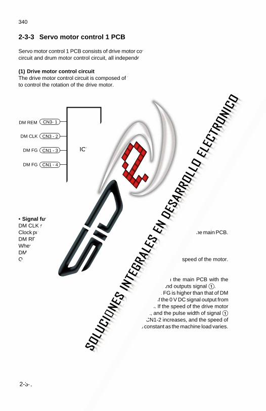
340
2-3-10
2-3-3 Servo motor control 1 PCB
Servo motor control 1 PCB consists of drive motor control circuit, fixing drive motor controlcircuit and drum motor control circuit, all independent from each other.
(1) Drive motor control circuitThe drive motor control circuit is composed of the components as shown in Figure 2-3-12to control the rotation of the drive motor.
CN3- 1 CN1 - 1
CN3 - 2
CN1 - 3
CN1 - 4
CN1 - 2
DM REM
DM CLK
DM FG
DM FG
Q1
24 V24 V
0 V
IC1
DM
1
Figure 2-3-12 Drive motor control circuit
• Signal functionsDM CLK signal (CN3-2): input signalClock pulse which is the reference signal for drive motor control. Output from the main PCB.DM REM signal (CN3-1): input signalWhen low, the drive motor (DM) is on.DM FG signal (CN1-3), (CN1-4): input signalsOutput from the pulse generator in the drive motor, and indicates the speed of the motor.
• Drive motor controlIC1 in Figure 2-3-12 compares the DM CLK signal output from the main PCB with thefrequency of the DM FG signals output from the drive motor, and outputs signal 1.If the speed of the drive motor is too high, the frequency of DM FG is higher than that of DMCLK, and the pulse width of signal 1 decreases. The width of the 0 V DC signal output fromCN1-2 decreases, and the speed of the drive motor drops. If the speed of the drive motoris too low, the frequency of DM FG is less than DM CLK, and the pulse width of signal 1increases. The width of the 0 V DC signal output from CN1-2 increases, and the speed ofthe drive motor increases. This keeps the motor speed constant as the machine load varies.
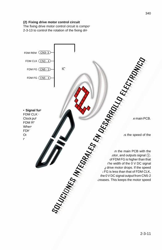
340
2-3-11
(2) Fixing drive motor control circuitThe fixing drive motor control circuit is composed of the components as shown in Figure2-3-13 to control the rotation of the fixing drive motor.
CN3- 3 CN5 - 1
CN3 - 4
CN5 - 3
CN5 - 4
CN5 - 2
FDM REM
FDM CLK
FDM FG
FDM FG
Q3
24 V24 V
0 V
IC3
FDM
1
Figure 2-3-13 Fixing drive motor control circuit
• Signal functionsFDM CLK signal (CN3-4): input signalClock pulse which is the reference signal for drive motor control. Output from the main PCB.FDM REM signal (CN3-3): input signalWhen low, the fixing drive motor (FDM) is on.FDM FG signal (CN5-3), (CN5-4): input signalsOutput from the pulse generator in the fixing drive motor, and indicates the speed of themotor.
• Fixing drive motor controlIC3 in Figure 2-3-13 compares the FDM CLK signal output from the main PCB with thefrequency of the FDM FG signals output from the fixing drive motor, and outputs signal 1.If the speed of the fixing drive motor is too high, the frequency of FDM FG is higher than thatof FDM CLK, and the pulse width of signal 1 decreases. The width of the 0 V DC signaloutput from CN5-2 decreases, and the speed of the fixing drive motor drops. If the speedof the fixing drive motor is too low, the frequency of FDM FG is less than that of FDM CLK,and the pulse width of signal 1 increases. The width of the 0 V DC signal output from CN5-2increases, and the speed of the fixing drive motor increases. This keeps the motor speedconstant as the machine load varies.

340
2-3-12
(3) Drum motor control circuitThe drum motor control circuit is composed of the components as shown in Figure 2-3-14to control the rotation of the drum motor.
CN3- 5 CN4 - 1
CN3 - 6
CN4 - 3
CN4 - 4
CN4 - 2
DRM REM
DRM CLK
DRM FG
DRM FG
Q2
24 V24 V
0 V
IC2
DRM
1
Figure 2-3-14 Drum motor control circuit
• Signal functionsDRM CLK signal (CN3-6): input signalClock pulse which is the reference signal for drive motor control. Output from the main PCB.DRM REM signal (CN3-5): input signalWhen low, the drum motor (DRM) is on.DRM FG signal (CN4-3), (CN4-4): input signalsOutput from the pulse generator in the drum motor, and indicates the speed of the motor.
• Drum motor controlIC2 in Figure 2-3-14 compares the DRM CLK signal output from the main PCB with thefrequency of the DRM FG signals output from the drum motor, and outputs signal 1.If the speed of the drum motor is too high, the frequency of DRM FG is higher than that ofDRM CLK, and the pulse width of signal 1 decreases. The width of the 0 V DC signal outputfrom CN4-2 decreases, and the speed of the drum motor drops. If the speed of the drummotor is too low, the frequency of DRM FG is less than that of DRM CLK, and the pulse widthof signal 1 increases. The width of the 0 V DC signal output from CN4-2 increases, andthe speed of the drum motor increases. This keeps the motor speed constant as themachine load varies.

340
2-3-13
2-3-4 Servo motor control 2 PCB
Servo motor control 2 PCB communicates serially with the main PCB. It receives commandsfrom the main PCB at input terminal DCM2PCB RXD and emits data at output terminalDCM2PCB TXD.
Main PCB (MPCB)
DCM2PCB RXD
DCM2PCB TXD
Servo motor control 2 PCB (DCM2PCB)
DCM2PCB RXD: signal from main PCB to servo motor control 2 PCB DCM2PCB TXD: signal from servo motor control 2 PCB to main PCB
Figure 2-3-15 Communication between servo motor control 2 PCB andmain PCB
Servo motor control 2 PCB consists of a CPU, external memory (ROM) and an addresslatch. The CPU and ROM are connected by the address bus used to read in data and thedata bus used to transfer data from outside the PCB to the CPU. The arrows in Figure 2-3-16show signal flow.The CPU processes input signals in accordance with the program in ROM and outputscontrol signals.
Output InputCPU IC8
ROM IC14
Address latch IC6
Figure 2-3-16 Servo motor control 2 PCB block diagram

340
2-3-14
(1) Original feed motor control circuitThe original feed motor control circuit consists of CPU IC8 and four FETs. The FETs turnon to operate the original feed motor in response to the on/off signal (PWM0/P34) and thedirection signals (OFM F ON and OFM R ON). The original feed motor turns in the normaldirection to move an original into the direction of exposure. The signals control motor actionas shown below.
CPU signals
OFM F ON OFM R ON PWM0/P34Motor action
H H
L H
H L
H, L Stops.
H Stops.
Turns in normal direction. Current flows from OFM+ to OFM–.
Stops.
Reverses.Current flows from OFM– to OFM+.
L
H
L
s
s
s ss
s
s
+–
+–
+–
s
CN4-1
CN4-2
OFM +
OFM –
R5
OFM ON
OFM ON
1 2
R84
R83
2 1
3
21
1 1
5 6
71
1
22
S G
R85
R86
R712
1
1
1 1
1
1
1
2
2 2
2
2
2
10 9
9
99
R72R70
8
R69
R82
3 4
IC12
IC15
IC15
IC15
IC15
2
2 215
IC5
76
5
3
3
3
33
3
14
4 13
R65
P G
P GP G
P G P G P GP G
1 122
R64
5 12
1
1
1
1
1
11
12
2
22
1
1
1
11
11
1
2
2
2
22
2
2
22
2
2
22
21
2
2
1
11
1 1
11
1
1
1
11
1
1
11
1
11
22
22
22
22
22
22
2
2
22
2
2R
3R
52
C
R50
R51
D11
D10
D D
FT3
D9
D8
D7
D6
D4
R2
DA
2DA
2
DA
3 DA
33
R6
C
FT5
SS
D17
D18
D19
R56
R55
R54
D27
D13
D20
D14
D15
FT4
R4
D26
D12
R53
C2
S G
24 V
R57
DD
G
PWM0/P34
IC8
FT2
D16
Figure 2-3-17 Original feed motor circuit

340
2-3-15
(2) Paper feed motor control circuitThe paper feed motor control circuit consists of CPU IC8 and an FET. When signal PWM1/P35 goes low, the FET turns on to drive the motor. When high, the FET turns off and themotor stops.When the PFM ON signal from the main PCB goes low, the paper feed motor is forced toturn.
CN3-1
CN3-2
P GP GP G
P G
P G
P G
G
CN2-8
S
SS
S
PFM +
PFM –
24 V
+
-
+2
2
2
22
2
2
22
2
2
2
2
2
22
2
2
2
C501
1
2211
1
1
1
1
1
1
1
11
1
1
1
11
1
1
1
3
3
3
3
DA1
DA1
FT1
R37
C1
D
S
R1
D1
D2
D3
D28
R38
R39
R40
IC5 R66 R67
IC15
164
R73
5 6
IC1
S GC21
2121 R35R25
R15
PFM ENA
PWM1/P35
IC8 R68
C51
C52
R32
Figure 2-3-18 Paper feed motor control circuit
(3) Reset circuitWhen reset signal (DCM2PCB RESET) from the main PCB goes low, or when IC3 detectsan abnormal 5 V supply, this circuit resets the CPU to prevent it from malfunctioning oraccepting invalid inputs.
s
s
CN2-5DCM2PCB RESET
1 2R12
1
1
12 2
2
R23 R339 8
IC2
5
4
6
1
2IC7IC7
3RESET
10 11 12 13
IC2 IC2
D21
R412
2
2
2
22
11
1
1
1
S G S G
R43
R42
2.2u
IC3
S GC3
3
+
+
3V cc
Out
GND
Figure 2-3-19 Reset circuit
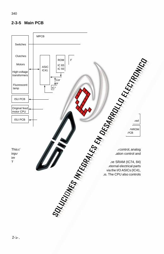
340
2-3-16
2-3-5 Main PCB
MPCB
Switches
Clutches
Motors
High-voltage transformers
Fluorescent lamp
Original feed motor CPU
ISU PCB
Commu- nication
Commu- nication
ISU PCB
ASIC IC41
ROM
IC 83
RAM
IC 74IC 84IC 93
CPU
IC 111 IC 102
IC110 IC22
Battery backup circuit
RESETReset circuit IC118
ASIC
Operation unit
Roll paper feed switches
LED printhead
LPHROM PCB
Image processing unit
Sensors
Analog signals
Figure 2-3-20 Main PCB block diagram
This circuit centers on the CPU (IC111) and includes the ROM and RAM, I/O control, analoginput/output, output buffer and signal level conversion, reset, communication control andimage processing unit circuits.The CPU controls the entire system based on the data written into the SRAM (IC74, 84)according to the control program in the ROM (IC83, 93). Driving of external electrical partsand input of signals from them are handled by the CPU I/O ports or via the I/O ASICs (IC41,102) connected to the CPU through the address bus and data bus. The CPU also controlsthe digital processor for the image processing unit.

340
2-3-17
(1) Fixing temperature error detection circuit
SG
R84
R85
R81
R159
C27 C26
C38R82 R87
R83
IC 3–
+
S
S
CN2-5
CN2-3
21
6 2 1 7
IC1A
IC20 IC20
1IC111
CPU
FTH1
GND
SG
R455
R454
R382
R383
TR3
SG
DI31S
CN4-17B
CN4-17ACN4-16B
R456
R457
R458S
33
2 12
TR2
MSW
SSW 3,4,5,6
24 V to PRY 1,2
5 V DC
5 V DC
5 V DC
5 V DCDI32
ASIC
IC41
41
42
R453
IC332Z-1
IC22
-26
Figure 2-3-21 Fixing temperature error detection circuit
The voltage from fixing thermistor 1 FTH1, which changes with the temperature, is input toterminal 1 of CPU IC111 and converted from analog to digital. This data is compared withthe conditions for displaying a service call C641 to determine if there is a fixing temperatureerror.The voltage from FTH1 is input to the inverting input terminal of comparator IC3. Thereference voltage formed by dividing 5 V DC across resistors R85 and R87 is input to thenon-inverting input terminal. Normally, the voltage input from fixing unit thermistor 1 ishigher than the reference voltage, so the IC3 output voltage is low. When the temperatureof the fixing section is abnormally high, the voltage from FTH1 drops below the referencevoltage, so the voltage at the output of IC3 goes high. This high level voltage passes througha 2-stage Schmitt trigger IC20 to be shaped. The output from IC20 is input to terminal 2 ofNAND gate IC1A.The main switch on signal (low level) is constantly input to terminal 2 of the NAND gate andwhen pin 3 goes high, the high-level voltage is output at terminal 1. This output voltage isconverted to 24 V DC by driver IC TR3 and input to the base of power relay drive transistorTR2 to force TR2 off. When TR2 turns off, power feed to the power relays PRY1, 2 is cutto turn them off.
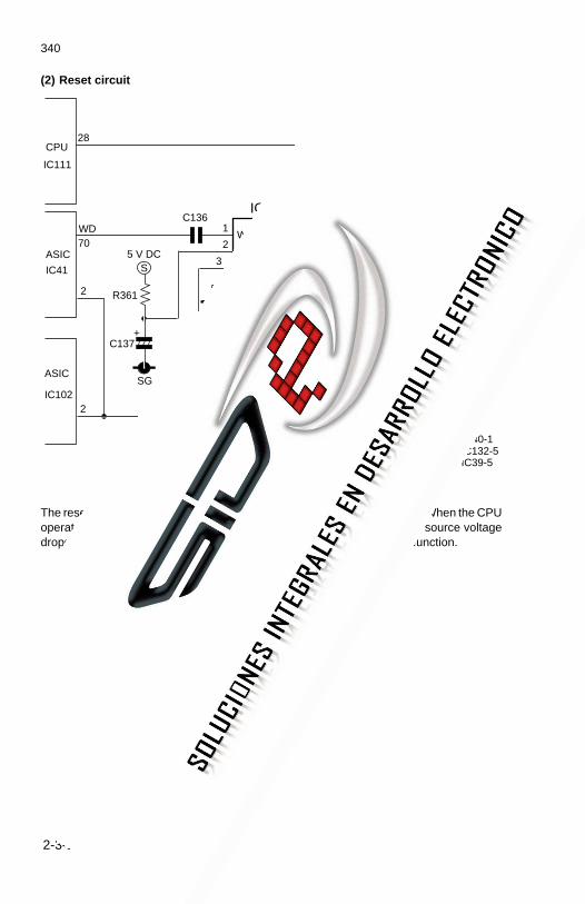
340
2-3-18
(2) Reset circuit
SG
WD
TC
ADJVCC
NC
_RES2
_RES1
GND
SG SG
1 2 3 4
S
+
S
S1
2
4
8
7
6
5
3
R362
R361
C137
C136
IC119 IC119
CP93
IC118 5 V DC
5 V DC
5 V DC
2IC102
ASIC
2
70
IC41
ASIC
28
IC111
CPU
RST
WD
IC40-2
RE
SE
T
9 8 11 10 13 12
IC119 IC119 IC119
IC40-1IC132-5IC39-5
3 4
IC119
Figure 2-3-22 Reset circuit
The reset circuit is comprised of system reset IC118 and peripheral circuits. When the CPUoperates abnormally, when the power is switched on, or when the power source voltagedrops, this circuit outputs a reset signal to the CPU to prevent CPU malfunction.

340
2-3-19
• System reset IC operation timing
4.25 V
4 V
2 V
0 V
0 V
0 V
0 VRES1
WD
TC
Vcc
12 3 654
Figure 2-3-23 System reset IC operation timing
1 When the power is switched on and the 5-V-DC power source voltage rises to 4.25 V,the potential of capacitor C137 connected to the TC pin of IC118 rises.
2 As the charging of C137 continues and the potential of the TC pin rises to 2 V, the outputlevel of the RES1 pin goes high. When the potential reaches 4 V, the pin goes low andC137 is discharged.
3 When the potential of the TC pin has dropped to 2 V as C137 discharges, RES1 goeshigh again.
4 Until the clock signal is input to the WD pin from the ASIC IC41, IC118 repeats the aboveoperation. When the clock signal is received, C137 is discharged while C118 clocksignal is high.
5 When the CPU operates normally, the clock signal is always input before the potentialof TC reaches 4 V in step 2, so RES1 remains high and is always kept high while thesystem is operating normally. If the CPU has a problem, and the clock is no longer inputwith the normal timing, the potential of IC137 rises to 4 V and RES1 goes low. This RES1signal goes through the 2-stage or 4-stage inverter IC119 and is input to the CPU andASIC reset pins, resetting the CPU automatically.
6 When the 5-V-DC power source voltage drops to 4.25 V, RES1 goes low and the CPUis reset.
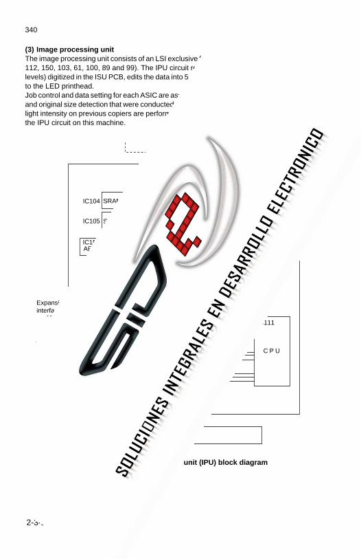
340
2-3-20
(3) Image processing unitThe image processing unit consists of an LSI exclusive for image processing (ASIC IC121,112, 150, 103, 61, 100, 89 and 99). The IPU circuit receives 8-bit image signal (256 tonelevels) digitized in the ISU PCB, edits the data into 5-bit signals (32 levels) and sends themto the LED printhead.Job control and data setting for each ASIC are assigned by the CPU. Auto exposure controland original size detection that were conducted by employing a halogen lamp with variablelight intensity on previous copiers are performed by controlling the digital image signals inthe IPU circuit on this machine.
IC103
IC99
IC112
IC121
IC114
IC61
IC150
IC104
IC105
Zoom processing
Input processing
Line correction
F I F O
ISU PCB
Filter processing
C P UGrayscale correction processing
IC100
IC111
IC89LED printhead
LED printhead
AE processing
SRAM
SRAM1
SRAM2
SRAM
FIF
O
SRAM
IC135.136
IC87.88IC78
IC64.67.79.80
IC42.43.44.60
Expansion interface 1
Expansion interface 2
Timing control
SRAM1-7
IC106.113 IC122.123 IC137.138
IC139
F I F O
control
Figure 2-3-24 Image processing unit (IPU) block diagram

340
2-3-21
• Input processing unitEight-bit image data from the ISU PCB is read into line FIFO memory (C114) line by line.Holding data of a total of 7 lines via SRAMs (IC106, 113, 122, 123, 137, 138 and 139), IC121conducts correction of the current line using the data of three lines on each side of it toeliminate any shift of the image in the sub scanning direction. Eight-bit image data issubjected to γ correction and black-and-while reversal at IC112.After that, the image data is sent to the zoom processing unit.
ISU PCB
MPCBS
PG
T
TC
LOC
K
ISU
D(7
: 0)
RE
SE
T D
SS
O-
ALE
A
(7 :
1)
D(7
: 0)
W
R :
RD
H
SY
NC
IC112
IC121
IC104
IC105
IDR
STR
IDC
LKDifferential IC
FIFO(5KB)
RESET HSYNC SCLK BE MRE CPU control
Input processing ID(7 : 0)
γ correction
MB interface PD
Black-and-white reversal
Address control
SRAM1(8KB)
SRAM2(32KB)
γ correction table
γ table selection, 1-line memory
Zoom processing
SRAM1-7
IC106.113 IC122.123 IC137.138
IC139
Figure 2-3-25 Input processing unit block diagram

340
2-3-22
• γ correction8-kbyte SRAM 1 (IC104) is used for γ correction where a γ table is selected for each pixelout of the 32 tables (8k/256). The γ table data is stored in 32-kbyte SRAM 2 (IC105) to beused for selection of the table to be read out of SRAM 1 (IC104).There are two modes available and can be selected via a register: one where a γ table isselected for every pixel and the other where it is fixed once selected.
• Black-and-white reversalBlack-and-white reversal is carried out by converting each 8-bit pixel data between 0 and1 for each bit.
0 0 0 0 0 0 1 1 1 1 1 1 0 0 0 0
1 1 1 1 1 1 0 0 0 0 0 0 1 1 1 1
1: Black pixel 0: White pixel
Main scanning direction
Black-and-white reversal
• AE processing unitHistograms of image data output from the input processing unit (IC112) are generated inthe AE processing unit (IC150).Based on sampled image data for the A4R/11" × 81/2" original, a histogram is created byanalyzing the data into 20 levels based on the line memory darkness data. The CPU selectsthe optimum dither matrix data based on this histogram.

340
2-3-23
• Zoom processing unitProcessing for enlargement or reduction in the main scanning direction in zoom mode orprocessing in the main scanning direction in independent zoom mode is conducted at thezoom processing unit (IC103) based on the magnification ratio data computed by the CPU.Then pixel data is added or deleted at certain intervals to determine the actual enlargementor reduction.Enlargement or reduction in the sub scanning direction is controlled by changing the originalfeed motor rotational speed which is done by servo motor control 2 PCB based on themagnification ratio data from the operation unit PCB.
ReductionImage data from the input processing unit (IC112) is sent to the zoom processing unit(IC103) where a clock is generated by extending the image clock by a certain interval. Theimage data at IC103 is written line by line into SRAM using this newly created clock.Because of this, the image data in the SRAM has lost pixels at the certain intervals. Whenthe data is read out of the SRAM sequentially using the image clock, line image data seemsto be reduced.
EnlargementImage data from the input processing unit (IC112) is sent to the zoom processing unit(IC103) where a clock is generated by extending the image clock by a certain interval. IC103then writes this image data into SRAM line by line. The image data is read out of the SRAMin synch with the newly created clock. Because of this clock, some of the pixels of the imagedata stay on the data bus twice (in case of magnification ratio of 200%) as long as with theimage clock.When this data is sampled in synch with the image clock while being read into the filterprocessing unit (IC16), they are sampled twice (in case of magnification ratio of 200%) andthe line image data is now enlarged in the main scanning direction.
• Image shiftingImage is shifted in the main direction by the zoom processing IC103 which changes theimage read-out start address or image read-out timing from the line memory based on theimage shift data from CPU IC111.
• Mirror imageMirror image processing in the main scanning direction is conducted by IC103 whichchanges the image read-out start address from the line memory based on the image shiftdata from CPU IC111 and reversing the read-out order.

340
2-3-24
• Filter processing unitWhen a mode is selected on the operation panel, the CPU sets a value corresponding tothat mode on the register. This starts image differentiation or integration to make a copy asclose to the original as possible by modifying the image continuity in accordance with thetype of the original used. For example, when a photograph is used as original, integrationis conducted at the filter processing unit. Differentiation is performed for originals with text.Integration and differentiation are conducted by IC61 and FIFO (256 kbytes × 4)(IC42, 43,44 and 60).
• Tone processing unitThe tone processing unit consists of IC100 and SRAM (IC87, 88). The unit applies toneprocessing to image data sent from the filter processing unit. It also conducts grayscalemodification from 256 to 32 levels for darkness control.

340
2-3-25
2-3-6 Backup PCB
MPCB
SRAM
BUPCB
Data bus Address bus
Control signals
Lithium battery backup power supply unit
5 V DC
Figure 2-3-26 Backup PCB block diagram
Backup PCB (BUPCB) consists of SRAM, lithium battery BT1 and backup battery powersupply unit and is connected to the main PCB with connectors. SRAM is connected to CPUIC111 on the main PCB via address bus, data bus and control signals. Normally the backupPCB is driven by the 5 V DC supplied from the main PCB. Once the power is shut off, or whenthe backup PCB is disconnected from the main PCB, the lithium battery (BT1) backupsupply unit takes over. The SRAM then enters the data hold mode where memory contentsare kept for extended periods of time at a power consumption rate of as low as a few µA.

340
2-3-26
2-3-7 ISU PCB
The ISU PCB consists of analog processing unit where original image data read by thecontact image sensor (CIS) is held for sampling and A-D-converted, shading correction unit,line forming unit where shading-corrected data is turned into line memory and a CPU incharge of data control for the respective ISU blocks.Image data from CIS is sent to the ISU PCB in synch with the ISU start signal. After beingprocessed there, the data is further sent to the image processing unit on the main PCB. TheCPU on the ISU PCB serially communicates with the CPU IC9 on the main PCB via TXDand RXD.
CH1 CH2 CH3 CH4
Analog processing unit
IC 1-4A-D conversion/
AGC processing unit AGCZ10×4
ADCCLKRESET/
RE
SE
T/
AGCCS1-4/ASB/
IOWR/IORD/
SI
AD0-7
ID1–4(7: 0)
FLFD
Main PCB
Txd
Rxd
9.83 MHz
CPU interface
IPU interface
CPU
WR
/RD
D0-7
A0-6
Reset IC
ISU
D0-7
SP
GT
,TC
LOC
K
HS
YN
C
CIS, AGC
interface
IC 11 IC29
IC28
IC31
IC30
Shading correction unit
ASIC
RA
M interface
Black reference value
White reference value
Line memory forming
Line memory forming
ISU
CIS
SI.CCLK. SHOLD.FLS
RAM
WDIC9
Figure 2-3-27 ISU PCB block diagram

340-1
2-3-27
(1) Analog processing unitFour analog signals from the contact image sensor for one-line image data are output to thebuffers of the analog processing unit in synch with start signal SI from the ISU PCB. As eachsensor output has a high impedance, it is converted into a low-impedance signal by thebuffer (IC42, 36, 34, 32) at the first stage. This signal is then held by the sample hold circuitin synch with the sample hold clock (SHOLD) from IC11 to isolate the image data voltage.The output from the sample hold circuit is non-inverting-amplified by IC41, 22, 19 and 16.As the voltage when the fluorescent lamp is on varies from channel to channel, gainadjustment is conducted at 4 V.FLDA (IC38) prepares data for fluorescent lamp light intensity measurement (sensor outputfor the status where the contact glass is covered with white tape). This data is fed to the mainPCB where it is A-D converted and comprared with the reference voltage.
CH1
IC42IC38
IC39
IC41
BufferFLDA
SHCLK
Non-inverting- amplification
Non-inverting- amplification
Non-inverting- amplification
Non-inverting- amplification
To MPCB
V
V
ID 1(7 : 0)AGCCS1
AGCZ10 IC3
AGCZ10 IC4
CH2
IC36
IC37
IC22
Buffer
SHCLK
V
V
ID 2(7 : 0)AGCCS2
AGCZ10 IC2
CH3
IC34
IC35
IC19
Buffer
SHCLK
V
V
ID 3(7 : 0)AGCCS3
Sample hold
AGCZ10 IC1
CH4
IC32
IC33
IC16
Buffer
SHCLK
V
V
ID 4(7 : 0)AGCCS4
Sample hold
Sample hold
Sample hold
Figure 2-3-28

340
2-3-28
(2) A-D conversion/AGC processing unitImage data from the contact image sensor is converted into 8-bit digital data by the A-Dconversion circuit IC1. When reference voltages for A-D conversion are set to 5 V and 0 V,the weight of the digital data (ID0 – ID7) is 5-0/256, i.e. about 19.5 mV. However the dataobtained using the white reference plate is smaller than 5 V for the absolute white. The blackreference data also is larger than 0 V. Therefore the actual range that can be used forgrayscale correction is narrow. AGC processing is conducted to expand this range to 0 to5 V whenever the copier main switch is turned on.
(3) Shading correction circuitDue to the dispersion in sensitivity of the photosensitive elements of the contact imagesensor, uneven fluorescent lamp light distribution and distortion in the lens, there is asignificant difference in the output voltage levels of the elements of the CIS. Shadingcorrection is conducted to eliminate this difference every time an original is fed on the copier(or the first original in multiple-original copying).
Black reference
value
Creation of black reference value
Shading ASIC peripheral devices
Shading ASIC
Creation of white reference value
Single line memory forming
CPU interface
IPU interface
Shading processing
White reference
value
Line memory forming
RAM
RAM0E1-4/
RAMWE1-4/
RAMA1(7:0)
RAMA3(7:0)
AD (7:0)
RAMA4(7:0)
RAMA1(7:0)
RAMA2(7:0)
RAMA3(7:0)
RAMA4(7:0)
RA
M interface
CIS, AGC
interface
SI.CCLK.SHOLD.FLS
ADCCLK
RESET/
AGCCS1-4/
ASB/
IOWR/
IORD/
ID1 (7:0)
ID2 (7:0)
ID3 (7:0)
ID4 (7:0)
D0-7
WR
/,RD
/,RE
SE
T
HS
YN
C
SP
OT
,TC
LOC
K
A0-6
ISU
D0-7
Line memory forming
Figure 2-3-29 Shading correction circuit block diagram

340
2-3-29
2-3-8 Operation unit PCB
The operation unit PCB consists of keyboard input circuit, LED lighting circuit and displaysection, all controlled by one-chip CPU IC1. This four-bit CPU controls the keyboard inputs,display LED on/off and display on the operation panel according to the programs installedon it.Data entered on the keyboard and data displayed on the LEDs and display section areprocessed as serial data and input to CPU IC111 at CN1-2 and output at CN1-4 in synchwith clock signal SCL at CN1-6.
CN1 - 6
CN1 - 2
CN1 - 4
CN8 - 6
CN8 - 2
CN8 - 3
CPU
IC1
Keyboard input circuit
LED lighting circuit
Display section
CPU IC111
Main PCB
Figure 2-3-30 Operation unit PCB block diagram

340-1
2-3-30
2-3-9 Inverter PCB
+24 V
Lighting signal (FL REM)
Intensity control signal (FL CONT)
CN1-4
CN1-3
CN1-2
CN1-1
CN2-1
CN2-2
CN2-5
CN2-6
FL
Figure 2-3-31 Inverter PCB block diagram
The inverter PCB consists of the high-frequency pulse generating circuit from which a high-frequency pulse of 37 kHz is emitted to the fluorescent lamp and the preheat circuit for thefluorescent lamp filaments.
• Functions of signalsFL REM (CN1-2), FL CONT (CN1-1): input signalsFluorescent lamp light intensity is controlled via the light intensity control signal (FL CONT)from the main PCB. When lighting signal FL REM is at low, 37-kHz pulse is generated fromthe high-frequency pulse generating circuit and sent to the fluorescent lamp to turn it on.Then, as the control voltage of the FL CONT is increased, the lamp grows brighter; and asit is decreased, the lamp becomes dimmer (see Figure 2-3-31).

Xi3648 (MCA) S/M
III S
et U
p an
d
Adj
ustm
ent S
ectio
n
III
SET UP ANDADJUSTMENT
SECTION

1-1-17
340
CONTENTS
3-1 Installation
3-1-1 Unpacking and installing the copier .................................................... 3-1-1(1) Installation environment .............................................................. 3-1-1(2) Installation procedure .................................................................. 3-1-2
3-1-2 Copy mode initial settings ................................................................. 3-1-273-1-3 Installing the key counter (optional) .................................................. 3-1-283-1-4 Attaching a roll unit heater (optional) ................................................ 3-1-31
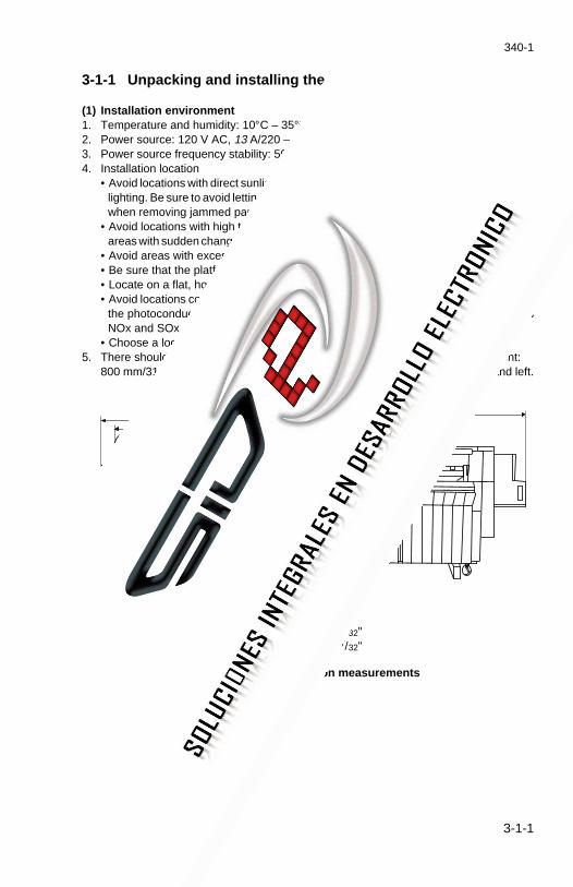
3-1-1
340-1
3-1-1 Unpacking and installing the copier
(1) Installation environment1. Temperature and humidity: 10°C – 35°C/50°F – 95°F, 15% – 85% RH2. Power source: 120 V AC, 13 A/220 – 240 V AC, 8 A3. Power source frequency stability: 50 Hz ± 0.3%, 60 Hz ± 0.3%4. Installation location
• Avoid locations with direct sunlight or bright areas such as near windows or with brightlighting. Be sure to avoid letting direct sunlight or bright light reach the photoconductorwhen removing jammed paper.
• Avoid locations with high temperature or humidity, low temperature or humidity, andareas with sudden changes in temperature. Also avoid areas with hot or cold draughts.
• Avoid areas with excessive dust or vibration.• Be sure that the platform or floor area can support the weight of the equipment.• Locate on a flat, horizontal surface (maximum inclination of 1°).• Avoid locations containing substances that could cause changes in the equipment or
the photoconductor (mercury, alkali or acid vapors, inorganic gases, gases such asNOx and SOx, and chlorine-based organic solvents).
• Choose a location with adequate ventilation.5. There should be sufficient space for operation and maintenance of the equipment:
800 mm/311/2" at front, 500 mm/1911/16" at right and 300 mm/1113/16" at rear and left.
DC
B
A
Figure 3-1-1 Installation measurements
A: 1590 mm/6219/32"B: 1168 mm/46"C: 1107 mm/4319/32"D: 1563 mm/6117/32"

3-1-2
340-3
(2) Installation procedure
Unpack the copier.
Remove main charger assembly, accessory case and retaining tape.
Attach the main charger assembly to the cleaning assembly.
Remove protection tape from the developing unit assembly and attach the developing unit cover.
Adjust the horizontal level of the unit.
Force the copier to stabilize (simulation 41).
Attach the flywheel assembly.
Attach the accessories.
Pour toner into the toner hopper assembly.
Add the starting developer (simulation 10).
Set the developer (simulation 60).
Adjust the position of the front covers.
Connect the power cord.
Remove spacers from the roll units and remove developing unit cover.
Adjust the fixing pressure.
Make a test copy.
Remove the tape retaining the cleaning unit weight.
Coat the cleaning blade with toner (simulation 40).
Installation of the copier completed.
Start

3-1-3
340-1
Unpack the copier.
1. Top pad 2. Inner case 3. Outer case 4. Main charger assembly 5. Dust cover 6. Machine body 7. Bottom pads 8. Skid 9. Front right pad10. Hinge joint11. Accessory case (see page
3-1-4 and Figure 3-1-3).12. Spacers (between the
upper and lower paperfeed guides of the 1st and2nd roll units).
13. Front cover pads(between each front coverand the copy bin).
14. Developing unit cover(secured with tape insidethe 2nd roll unit).
15. Inner pads16. Top board17. Caster lever
(Item No.: 67802210)18. Flywheel assembly19. Bronze binding screws,
M4 × 8 (3)20. Top case21. Front left pad22. Props
Figure 3-1-2 Unpacking
4
3
¤
¤
¤
1
2
5
6
%
7
8
⁄0
&*(
%
!@
97
#$
)
^
0

3-1-4
340
1. Paper roll shafts2. Original loop guide3. Tray stoppers (2)4. Accessory spacer
Figure 3-1-3 Accessory case
5. Accessory case6. Main unit support plates (2)7. Main unit support covers (2)
1
2
4
5
67
3

3-1-5
340-3
1. Remove the 14 hinge joints.2. Remove the top case, outer case, inner case, top board, top pad, four props, front
right pad, and dust cover (see Figure 3-1-2).3. Remove the tape retaining the front covers and copy bin.4. Open the copy bin and remove the front cover pads (1 each on the right and left side)
between the copy bin and the front covers. Remove the tapes from the front covermagnets.
5. Remove the front cover retainers (1 each on the right and left side: 4 screws).
Front cover retainer
Front cover pad
Tape
Front cover padTape
Figure 3-1-4

3-1-6
340-3
6. Open the front cover.7. Remove the two screws on the stopper support plate attached to each front cover
and remove a screw on the earth wire.8. Lift a front cover, and pull out the pin on the front cover from the hinge on the main
unit to detach the front cover. Remove the other front cover in the same manner.
Hinge
Front cover
Stopper support plate
Earth wire
Hinge
Figure 3-1-5
9. Attach the machine bolts to the holes (2 locations each on the front and rear) in themain unit.• Machine bolts are optional. (Item No.: 67868010).
Machine bolt
Machine bolt
Figure 3-1-6

3-1-7
340-3
10. Pass a rope through the machine bolts attached to the front and rear of the right sideof the main unit.
11. Lift the right side of the main unit with the rope to remove the bottom pad.12. Remove the rope.13. Pass the rope through the machine bolts attached to the front and rear of the left
side of the main unit.14. Lift the left side of the main unit with the rope to remove the bottom pad.15. Lift the left side of the main unit with the rope again and carefully lower the left side
of the main unit from the skid.• When removing the main unit from the skid, check that the nuts for adjusting height
are completely tightened (with no space between each nut and the bottom baseof the main unit). If you attempt to move the main unit when the nuts are notcompletely tightened, it may cause problems such as bending a bolt on the caster.
16. Remove the rope and pass it through the machine bolts attached to the right sideof the unit again. Lift the right side of the main unit and carefully lower the main unitfrom the skid.
17. Remove the rope.18. Detach the machine bolts from the main unit.
Bottom pad
Skid
Rope
Figure 3-1-7

3-1-8
340-3
Remove the main charger assembly, accessory case and retaining tape.
1. Remove the main charger assembly secured to the original holding section withtape.
2. Take out the accessory case placed on the base assembly of the main unit.3. Remove the tape retaining the original guide.4. Remove the tape retaining the left and right paper eject guides.5. Remove the tape retaining the power cord at machine rear.6. Remove the two tapes retaining the original holding section.7. Open the original holding section and remove the two pads at the right and left.
Accessory case
TapeMain charger assembly
Figure 3-1-8

3-1-9
340-1
Remove spacers from the roll units and the developing unit cover.
1. Pull out the 1st roll unit.2. Release the roll paper upper guide in the direction of the arrow by holding the roll
paper insertion knobs.3. Remove the roll unit spacer retained by tape.4. Return the roll paper upper guide to the original position.5. Insert the 1st roll unit back in the original position in the main unit.
Roll paper insertion knob
Roll paper insertion knob
Roll unit spacer
Roll paper upper guide
Figure 3-1-9
6. Pull out the 2nd roll unit.7. Release the roll paper upper guide in the direction of the arrow by holding the roll
paper insertion knobs.8. Remove the roll unit spacer.9. Return the roll paper upper guide to the original position.
10. Remove the developing unit cover attached to the bottom of the 2nd roll unit withtape.
11. Insert the 2nd roll unit back in the original position in the main unit.
Roll paper insertion knob
Roll unit spacer
Developing unit coverRoll paper upper guide
Figure 3-1-10

3-1-10
340
Remove the tape retaining the cleaning unit weight.
1. Open the original holding section.2. Pull the main unit release lever to open the main unit.3. Remove the tape retaining the cleaning unit weight.4. Close the original holding section.
Cleaning unit weight
Figure 3-1-11
Attach the flywheel assembly.
1. Remove the screw from the upper right side cover and open the cover.2. Align the notches in the flywheel assembly with the projections on the flywheel
mount, and push the flywheel assembly into the main unit.3. Align the screw holes in the flywheel assembly and the mount, and insert and
tighten 3 M4 × 8 bronze binding screws.
Flywheel assembly
Flywheel mount
Upper right side cover
M4 × 8
Screw
Figure 3-1-12

3-1-11
340
Attach the main charger assembly.
1. Remove the 9P connector on the cleaning unit assembly.
9P connector
Figure 3-1-13
2. Open the right cover.3. Push the toner collection pipe downward until it is held by the pin and locked in
place.
Toner collection pipe
Pin
Figure 3-1-14

3-1-12
340
4. Remove the M3 × 8 screw holding the cleaning unit retention stopper.5. Slide the cleaning unit retention stopper in the directions of the arrows 1 and 2
to unlock the stopper plate.6. Pull the cleaning assembly toward you and remove the cleaning assembly from the
main unit.
ca
12
Cleaning assembly
Stopper plate
Cleaning unit retention stopper
M3 × 8
Figure 3-1-15

3-1-13
340
7. Loosen the two M4 × 8 screws holding the stopper plate, slide the plate all the wayto the left and retighten the screws.
M4 × 8
Cleaning unit retention stopper
Stopper plate
Figure 3-1-16
8. Fit the main charger assembly to the cleaning assembly by engaging the hinge onthe main charger assembly with the groove in the cleaning unit retention stay. Thenpush the main charger assembly in the direction of the arrow.
Cleaning assembly
Cleaning unit retention stay
Main charger assembly
Figure 3-1-17

3-1-14
340
9. Attach the cleaning assembly to the main unit by inserting the cleaning unit retentionstay in the larger hole in the rear of the left side plate of the main unit. (The smallhole in front side is for shipment).
Hole to be used for shipment
Be sure to use this hole.
Figure 3-1-18
10. Slide the cleaning unit retention stopper to the left until it is held by the notch in thestopper plate. Tighten the stopper with an M3 × 8 screw.
M3 × 8 Stopper plate
Cleaning unit retention stopper
Figure 3-1-19
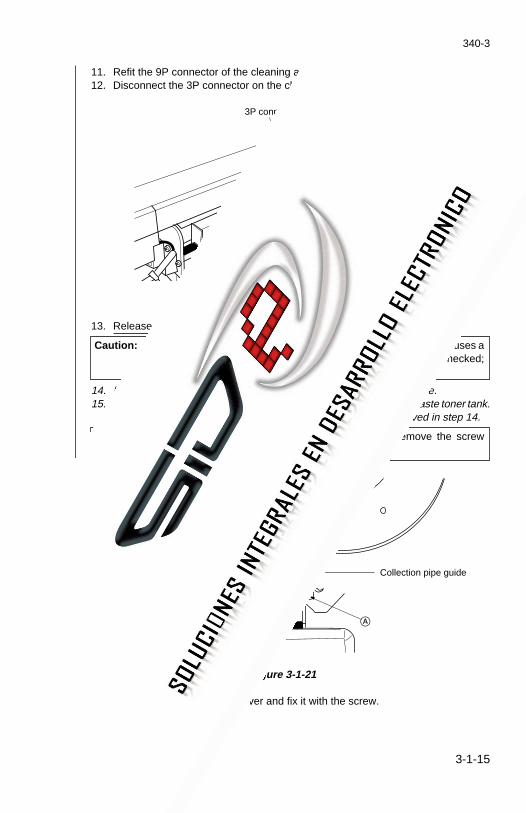
3-1-15
340-3
11. Refit the 9P connector of the cleaning assembly to its original position.12. Disconnect the 3P connector on the cleaning solenoid.
3P connector
Cleaning solenoid
Figure 3-1-20
13. Release the toner collection pipe.
Caution: Closing the right cover without releasing the toner collection pipe causes amessage to be displayed requesting that the waste toner tank be checked;copying is also disabled.
14. Remove the screw M4 × 6 in position A on the collection pipe guide.15. Remove the waste toner tank sponge assembly taped beside the waste toner tank.
Secure the assembly in position B with the screw M4 × 6 removed in step 14.
Caution: To detach the cleaning assembly for maintenance, remove the screwM4 × 6 and push the toner collection pipe down.
Collection pipe guide
A
M4 × 6
Toner collection pipe
B
Waste toner tank sponge assembly
Figure 3-1-21
16. Close the upper right side cover and fix it with the screw.17. Close the right cover.18. Close the main unit.

3-1-16
340-1
Remove the protection tape from the developing unit assembly.
1. Loosen the two upper rear cover pins and open the upper rear cover.2. Remove the two screws from the upper rear cover and a screw from the earth wire
to remove the upper rear cover from the main unit.
Earth wire
Upper rear cover pins
Upper rear cover
Figure 3-1-22
3. Remove the lower rear cover (four screws).4. Disconnect the 1P connector and the 7P connector on the developing unit
assembly.
1P connector
7P connector
Figure 3-1-23

3-1-17
340-1
5. Loosen the screws of the developing unit retention plates attached on the left andright of the developing unit lower partition and rotate the developing unit retentionplates toward the front.
Screw
Developing unit retention plate
Figure 3-1-24
6. Detach the developing unit assembly from the main unit.7. Disconnect the 3P connector from the toner feed motor.8. Detach the toner hopper assembly from the developing unit assembly.9. Remove the developing unit protection tape from both ends of the magnet roller.
Developing unit protection tape Toner hopper assembly
3P connector
Developing unit protection tape
Figure 3-1-25

3-1-18
340-1
Attach the developing unit cover to the developing unit assembly.
1. Remove the clamp (1 screw) attached to the right side of the developing unit cover.
Developing unit cover
Clamp
Screw
Figure 3-1-26
2. Insert the pin on the left side of the developing unit cover in the hole in the developingunit left plate to attach the cover to the developing unit assembly.
3. Use the clamp removed in step 1 to hold the wires as shown in Figure 3-1-27 andretain with the screw, being careful not to trap the wires. Check that there is no gapbetween the developing unit cover and the developing unit frame.
Pin Developing unit cover
Clamp
Screw
Figure 3-1-27

3-1-19
340
Adjust the horizontal level of the unit.
1. Place a level on the developing unit lower partition and check that the unit ishorizontal in all the directions. If not adjust the adjustment nuts with the caster lever(Item No.: 67802210).
2. Attach the developing unit assembly to the main unit with the assembly pushed allthe way to the machine left and secure with the developing unit retention lever.
3. Return the developing unit retention plates to the original positions and tighten theirscrews to secure. Before tightening the screws, make sure that the developing unitassembly is located all the way to the left of the main unit and the gear of thedeveloping unit assembly meshes well with the gear of the main unit.
4. Connect the 1P connector and 7P connector on the developing unit assembly.
Attach the front covers and adjust the positions.
1. Attach the front covers to the main unit.2. Open and close the front covers and check that there is no problem.
* The front cover top edges and the edge of the bypass table should be on the samelevel.The switch contact plate should be securely inserted in the notch on the bypasstable.
3. In case of abnormalities, adjust the positions of the front covers in the followingprocedure:• If a front cover is misaligned in the left/right direction
Loosen the 2 screws A each on the top and bottom hinges, and move the frontcover to the left or right to adjust, using the calibration marks engraved on thehinge section (long hole between the screws).
• If a front cover is misaligned in the up/down directionLoosen the 2 screws B each on the top and bottom hinges and move the frontcover up or down to adjust, using the calibration marks on the frame.
Screw B
Screw A
Screw A
Screw B
Figure 3-1-28

3-1-20
340
Adjust the fixing pressure.
1. Pull the main unit release lever to open the main unit.2. Open the front covers.3. Detach the front left and right removal covers (1 screw each).4. Tighten the fixing unit pressure adjustment nuts until they are fast.5. Reinstall the front left and right removal covers.6. Remove the left cover (7 screws).7. Close the main unit.8. Close the front covers.
Front left removel cover
Fixing unit pressure adjustment nut
Front right removal cover
Figure 3-1-29
Connect the power cord.
1. Connect the power cord to a wall outlet.

3-1-21
340
Force the copier to stabilize (simulation 41) .
1. Force safety switch 6 on.2. Turn the main switch on.3. Enter 10871087 with the numeric keys to enter the simulation mode.4. Enter 041 with the numeric keys.5. Press the enter key. The copier enters the forced stabilization mode.
Safety switch 6
Figure 3-1-30

3-1-22
340
Add the starting developer (simulation 10).
Caution: Before adding the starting developer, ensure that developing unit assemblyis located all the way to the machine left and the gear of the developing unitassembly meshes well with the gear of the main unit.
1. Shake the bottle of starting developer well to mix the developer.2. Input 010 with the numeric keys.3. Press the enter key. The unit starts operating.4. Evenly pour the contents of 1 bottle of starting developer into the developing unit
assembly.5. After pouring, press the stop/clear key. The unit stops operating.
Developer bottle
Figure 3-1-31
6. Attach the toner hopper assembly to the developing unit assembly. Do not connectthe 3P connector of the toner feed motor yet.
7. Release safety switch 6 to turn it off.8. Refit the rear upper cover.

3-1-23
340
Set the developer (simulation 60).
1. Input 060 with the numeric keys.2. Press the enter key.
• The unit starts operating. When 3 minutes have elapsed since the start ofoperation, the toner control voltage is automatically set and the value is shown onthe display.
• Do not apply shock or vibration to the main unit while it is operating.• The displayed value should be written on the simulation label.
Coat the cleaning blade with toner (simulation 40).
1. Pull the main unit release lever to open the main unit.2. Refit the left cover (7 screws).3. Connect the 3P connector of the cleaning solenoid and close the main unit.4. Input 040 with the numeric keys.5. Press the enter key.
• After approximately 35 seconds have elapsed, the chime sounds and coating oftoner on the cleaning blade is finished.
6. Turn the main switch off and on to cancel the forced stabilization mode and exit thesimulation mode.

3-1-24
340
Pour toner into the toner hopper assembly.
1. Fit the 3P connector of the toner feed motor.2. Shake a toner bottle well from side to side and up and down to mix the contents.3. Remove the seal from the cap of the toner bottle.
Figure 3-1-32
4. Open the hopper lid. Squeeze the tabs on both sides of the toner bottle cap andplace the bottle, upside down, over the cartridge slot in the toner hopper on themachine right (see the figure).
Figure 3-1-33

3-1-25
340-1
5. Hold the bottle at the lower part of it with one hand; slide the bottle to the machinecenter and then back to the original position four or five times while tapping thebottom with the other hand.
Figure 3-1-34
6. Hold the tabs at both ends of the bottle cap and pull the bottle away from themachine.
Figure 3-1-35
7. Pour toner into the toner hopper assembly in the same manner for the left side ofthe machine.
8. Put the hopper lid back in place.9. Close the upper rear cover and retighten the pins.
10. Reinstall the lower rear cover.

3-1-26
340
Attach the accessories.
1. Attach the loop guide to the main unit by engaging the grooves in the loop guide withthe two pins on the upper rear cover.
2. Open the copy bin and attach the tray stoppers to the left and right front covers byhanging the tray stopper claws in the tray stopper holes matching the desired size.
3. Close the copy bin.4. Open the front covers.5. Use the four M4 × 6 binding bronze screws that were used to install the front cover
retainers to attach the 2 support assemblies to the main unit.6. Close the front covers.
Main unit support assembly
Figure 3-1-36
Make a test copy.
Completion of installation of the copier.
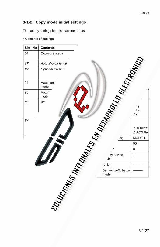
3-1-27
340-3
3-1-2 Copy mode initial settings
The factory settings for this machine are as shown below.
• Contents of settings
Sim. No. Contents Setting at factory Settings
84 Exposure steps 13 1: 13STEPS
87 Auto shutoff function Present 1: ON
89 Optional roll unit Not installed 1: NOCON-NECT
94 Maximum copy length for multiple copy 1400 mm 1400mode
95 Maximum copy length for roll/bypass 5000 mm 5000mode
96 Action after paper empty detectionPlain paper 10 s 10 sTracing paper (vellum) 10 s 10 sFilm 1 s 1 s
97 Switching between front and rear ejectionof originals
Single copy Rear ejection 1. EJECTContinuous copy Front ejection 2. RETURN
98 Copy count timing During feeding MODE 1
User Auto clear time 90 s 90setting Auto shutoff function Present 0
Preheat/energy saving mode Energy saving 1mode
Initial size mode A size ———
Initial copy mode Same-size/full-size ———mode

3-1-28
340-3
3-1-3 Installing the key counter (optional)
Note that the following part is required in installing a key counter:Key counter socket assembly (Part No. 41529210)
Procedure1. Open the right cover.2. Detach the right front cover.3. Remove the three screws and detach the main switch assembly.4. Remove the shorting plug from the 4P connector for the main unit key counter.
Shorting plug
4P connector for key counter
Main switch assembly
Figure 3-1-37

3-1-29
340
5. Remove the two screws (the lower one is fastened with a nut from the rear side) anddetach the key counter cover.
6. Using the two screws removed in step 5, attach the key counter socket to the main switchassembly. Secure the lower screw from the rear with the nut.
7. Connect the 4P plug for the key counter socket to the key counter 4P connector on themain unit.
Nut
Key counter cover
Nut
Key counter socket
4P plug
To be connected to the 4P connector from which the shorting plug has been detached
Figure 3-1-38

3-1-30
340
8. Reattach the main switch assembly to the main unit. 9. Refit the right front cover on the main unit.10. Close the right cover.11. Plug the power cord to a wall outlet then turn the main switch on.12. Run simulation 82 and set KEY-CARD to 0.13. Check that when the key counter is removed, “Insert key counter” is shown on the
display.14. Insert the key counter, make a test copy and check that the number of copies is counted
correctly.

1-1-19
340-3
CONTENTS
3-2 Simulation
3-2-1 Simulation function .............................................................................. 3-2-1(1) Running a simulation ................................................................... 3-2-1(2) Simulation list .............................................................................. 3-2-2(3) Contents of simulations ............................................................... 3-2-8
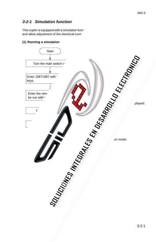
3-2-1
340-3
3-2-1 Simulation function
This copier is equipped with a simulation function which can be used to check the operationand allow adjustment of the electrical components.
(1) Running a simulation
Start
Turn the main switch on.
Enter 10871087 with the numeric keys.
Enter the simulation number to be run with the numeric keys.
Press the enter key.
The simulation is run.
Enter 001 and press the enter key or turn the main switch off and back on.
End
- - - - - - Entering the simulation mode.
- - - - - - - - - - - - - - - - - - - 000 is shown on the display.
- - - - - - Selecting a simulation number.
- - - - - - Exiting the simulation mode.
- - - - - - - - - - - - - - - - - - - The selected simulation No. is displayed.

3-2-2
340-3
SectionSim.
Simulation contents DefaultNo.
(2) Simulation list
All
Paperfeed/conveying
01 Exiting simulation mode
03 Copying with original but no paper
04 Checking paper feed clutch operation
Names of clutches and order of activation:
1. Upper feed clutch
2. Middle feed clutch
3. Lower feed clutch (optional)
05 Checking winding clutch operation
Names of clutches and order of activation:
1. Upper roll winding clutch
2. Middle roll winding clutch
3. Lower roll winding clutch (optional)
06 Checking roll paper conveying/registration clutchoperation
Names of clutches and order of activation:
1. Roll conveying clutch
2. Registration clutch
07 Checking cutter clutch operation
08 Checking bypass clutch operation
Name of clutch:
Bypass registration clutch
———
———
———
———
———
———
———
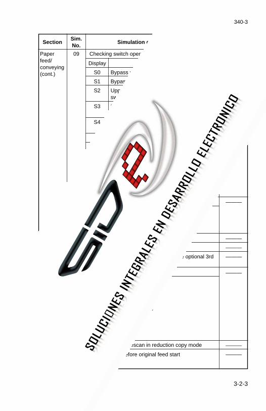
3-2-3
340-3
SectionSim.
Simulation contents DefaultNo.
Paperfeed/conveying(cont.)
09 Checking switch operation
Display Switch
S0 Bypass registration switch
S1 Bypass timing switch
S2 Upper roll paper leading edge detectionswitch
S3 Middle roll paper leading edge detectionswitch
S4 Lower roll paper leading edge detectionswitch (optional)
S5 Registration switch
S6 Paper conveying switch
S7 Eject switch
PE Fixing unit pulse sensor
P2 Upper pulse sensor
P3 Middle pulse sensor
P4 Lower pulse sensor (optional)
10 Checking drive motor operation
Names of motors:
1. Drive motor
2. Fixing motor
11 Checking paper feed motor operation
12 Checking counter operation
17 Checking the lower roller unit (when the optional 3rdroll unit is installed)
18 Checking fan motor operation
Names of motors:
LPH fan motor 1
LPH fan motor 2
Paper conveying fan motor
Cooling fan motor
Right fixing fan motor
Left fixing fan motor
25 Adjustment for prescan in reduction copy mode
26 Setting delay before original feed start
———
———
———
———
———
———
———
———

3-2-4
340-3
SectionSim.
Simulation contents DefaultNo.
Paperfeed/conveying(cont.)
Optical
Charging
Cleaning
53 Adjusting 100% magnification
54 Adjusting leading edge registration
55 Adjusting synchrocut length (297 mm)
56 Adjusting synchrocut length (1189 mm)
57 Adjusting the leading edge margin
58 Adjusting the trailing edge margin/displayedsynchrocut length
59 Adjusting the paper cut position for specified lengthcut mode
21 Checking original size detection operation
Display Original size
ORG SIZE L B2/24" or larger
ORG SIZE M B2 – B3/24" – 22"
ORG SIZE S A3/18" or smaller
22 Checking original detection switch operation
Display Switch
S1 Original leading edge detection switch
S2 Original trailing edge detection switch
24 Checking original feed motor operation
31 Ignoring developing control
33 Turning the transfer charger on
34 Turning the separation charger on
35 Entering drum surface potential data for black &white mode
36 Entering drum surface potential data for half-tonemode
39 Displaying the thermistor outputs
40 Coating the cleaning blade with toner
45 Checking cleaning solenoid operation
48 Checking separation claw solenoid operation
———
———
———
———
———
———
———
———
———
———
———
———
———
TRGT: 224LPH_ON:
18
TRGT:191LPH: 9
———
———
———
———
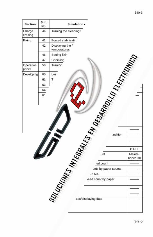
3-2-5
340-3
SectionSim.
Simulation contents DefaultNo.
Chargeerasing
Fixing
Operationpanel
Developing
Memoryinitialize
Counts
Counts
44 Turning the cleaning lamps on
41 Forced stabilization
42 Displaying the fixing unit thermistor detectiontemperatures
46 Setting fixing stabilization at low speed
47 Checking fixing heater operation
50 Turning all the operation unit LEDs on
60 Loading developer
61 Turning developing bias on
63 Checking/changing toner control voltage
64 Checking toner feed motor operation
65 Displaying toner sensor output
Display description:
Toner sensor output value
Toner sensor output value after temperaturecompensation
Temperature detected by the developing unitthermistor
66 Entering toner sensor control level/copy count
67 Selecting operation under the empty toner condition
70 Initializing backup memory 1
71 Selecting the maintenance cycle
72 Setting/clearing the maintenance count
73 Displaying/clearing total paper feed count
74 Displaying/clearing the jam counts by paper source
75 Entering the service telephone No.
76 Displaying/clearing paper feed count by papersource
77 Clearing the counts
78 Displaying set data
79 Specifying addresses/displaying data
———
———
———
———
———
———
———
———
———
———
———
———
———
———
1: OFF
Mainte-nance 30
———
———
———
———
———
———
———
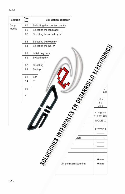
3-2-6
340-3
SectionSim.
Simulation contents DefaultNo.
Copymodes
CIS
Imagepositionalignment
80 Switching the counter counting units
81 Selecting the language
82 Selecting between key counter/card
83 Selecting between metric/inch
84 Selecting the No. of exposure steps
85 Initializing backup memory 2
86 Switching the fixing temperature
87 Disabling cancellation of the auto shutoff function
89 Setting optional roll unit
92 Setting potential correction intervals
94 Setting the maximum copy length for multiple copymode
95 Setting the maximum copy length for roll/bypassmode
96 Selecting the action after paper empty detectionPlain paperFilmTracing paper
97 Switching between front and rear ejection of originalsSingle copyContinuous copy
98 Selecting the copy count timing
99 Displaying the ROM versions
109 Setting the controller type
110 Checking fluorescent lamp operation
111 Checking shading compensation operation
112 Checking AGC processing operation
113 Setting the shading mode
120 Adjusting γ correction
121 Adjusting gain
132 Adjusting optical axis
133 Adjusting the image width in the main scanningdirection
———
———
KEY-CARD: 0
———
1: 13STEPS
———
2:OTHERS
1: ON
1: NOCONNECT
3: 20 m
ORGMAX: 1400
PAPERMAX: 5000
10 s1 s10 s
1: EJECT2: RETURN
MODE: 1
———
1. TYPE A
———
———
———
———
———
———
0 mm
0 mm
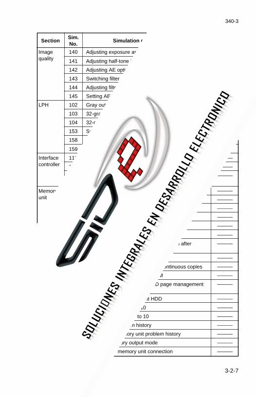
3-2-7
340-3
SectionSim.
Simulation contents DefaultNo.
Imagequality
LPH
Interfacecontroller
Memoryunit
140 Adjusting exposure amount
141 Adjusting half-tone image quality
142 Adjusting AE optimum level
143 Switching filter modes
144 Adjusting filter gain
145 Setting AE fine adjustment intervals
102 Gray output
103 32-gradation output
104 32-gradation output (without compensation)
153 Selecting current correction value
158 Adjusting focus
159 Solid black test pattern output
115 Selecting the connection to the interface controller
116 Setting the time to return from the offline condition
117 Adjusting the leading edge registration (whenconnected to the interface controller)
160 Adjusting base 4 output density
161 Adjusting thresholds (central exposure level)
162 Adjusting base 4 thresholds simultaneously
163 Adjusting Exp. 1.0 threshold
164 Adjusting Exp. 7.0 threshold
165 Setting the memory unit connection
166 Selecting display of the “Output?” screen afterrestart
167 Setting the AE scan
168 Setting the maximum number of continuous copies
170 Checking the memory unit DRAM
172 Checking the memory unit HDD page managementarea
173 Formatting the memory unit HDD
174 Clearing programs 6 to 10
175 Restoring programs 6 to 10
176 Memory unit problem history
177 Clearing the memory unit problem history
178 Selecting memory output mode
179 Checking the memory unit connection
———
———
———
———
———
3
———
———
———
———
———
———
———
———
———
———
———
———
———
———
———
———
———
———
———
———
———
———
———
———
———
———
———

3-2-8
340-3
Sim.No.
Description
01 Exiting simulation mode
DescriptionExits simulation mode and returns to normal mode.
PurposeUsed when closing simulation mode.
MethodPress the enter key. The copier returns to the normal mode.
03 Copying with original but no paper
DescriptionMakes copies without feeding paper.
PurposeTo check general machine operation.
Method1. Remove the paper, if any, from the paper source device that was used
before starting this simulation.
2. Press the enter key. The copier waits for an original to be placed inposition.
3. Put an original in place. The machine scans the original and displays theoriginal length. Continuous simulated copying of the original then starts.
CompletionPress the stop/clear key. Copying stops when the original return step iscompleted for the current cycle.
(3) Contents of simulations

3-2-9
340-3
Sim.No.
Description
04 Checking paper feed clutch operation
DescriptionOperates the upper, middle and lower feed clutches individually.
PurposeTo check the operation of the paper feed clutches when the primary paperfeed fails.
MethodPress the enter key. The feed clutches are activated one by one in thefollowing order and each remains on for 4 seconds. The paper feed motoralso turns on.
Upper feed clutchMiddle feed clutchLower feed clutch (optional)
• To interrupt the simulation, press the stop/clear key.
CompletionPress the stop/clear key.
05 Checking winding clutch operation
DescriptionOperates the upper, middle and lower roll winding clutches individually.
PurposeTo check operation of the roll winding clutches when a problem arises whilewinding roll paper.
MethodPress the enter key. The roll winding clutches are activated one by one inthe following order and each remains on for 4 seconds. The paper feedmotor also turns on.
Upper roll winding clutchMiddle roll winding clutchLower roll winding clutch (optional)
• To interrupt the simulation, press the stop/clear key.
CompletionPress the stop/clear key.

3-2-10
340-3
Sim.No.
Description
06 Checking roll paper conveying/registration clutch operation
DescriptionOperates the roll paper conveying and registration clutches individually.
PurposeTo check the operation of the roll paper conveying clutch and registrationclutch when the secondary paper feed fails.
MethodPress the enter key. The following clutches are activated one by one in thefollowing order and each remains on for 4 seconds. The paper feed motoralso turns on.
Roll conveying clutchRegistration clutch
• To interrupt the simulation, press the stop/clear key.
CompletionPress the stop/clear key.
07 Checking cutter clutch operation
DescriptionOperates the cutter clutch.
PurposeTo check the cutting operation of rolled paper.
MethodPress the enter key. The cutter clutch is turned on. The paper feed motoralso turns on.
• After the cutter clutch has turned once, the related components turn off.
CompletionPress the stop/clear key.
08 Checking bypass clutch operation
DescriptionOperates the bypass registration clutch.
PurposeTo check operation of the bypass registration clutch when the bypass feedfails.
MethodPress the enter key. The bypass registration clutch is turned on. The paperfeed motor also turns on.
CompletionPress the stop/clear key.

3-2-11
340-3
Sim.No.
Description
09 Checking switch operation
DescriptionChecks the actions of the switches on the paper path by feeding paper.
PurposeTo check switches when paper jams.
Method1. Press the enter key.
2. Select the paper source by pressing the paper source key.
3. Press the enter key. Paper feed starts and the actions of the switchescan be checked. “∗” is shown, starting at the extreme left; it movestoward the right as each switch is turned on.
Bypass mode: S0 S1 S6 S7 PE1st roll unit (LED1): S2 S5 S6 S7 P2 PE2nd roll unit (LED2): S3 S5 S6 S7 P3 PE3rd roll unit (LED3): S4 S5 S6 S7 P4 PE
The actions of the following switches are checked.S0: Bypass registration switchS1: Bypass timing switchS2: Upper roll paper leading edge detection switchS3: Middle roll paper leading edge detection switchS4: Lower roll paper leading edge detection switch (optional)S5: Registration switchS6: Paper conveying switchS7: Eject switchPE: Fixing unit pulse sensorP2: Upper pulse sensorP3: Middle pulse sensorP4: Lower pulse sensor (optional)
CompletionPress the stop/clear key.
10 Checking drive motor operation
DescriptionOperates the drive motor. This simulation can be run after machine stabiliza-tion. To run this simulation before machine stabilization, run simulation 41 first.
PurposeUsed when loading the developer to drive the developing section.
MethodPress the enter key. The drive motor, the fixing motor, developing bias andpre-charging lamp turn on.
CompletionPress the stop/clear key to stop the components.

3-2-12
340-3
Sim.No.
Description
11 Checking paper feed motor operation
DescriptionOperates the paper feed motor.
PurposeTo check the drive in the paper feed section.
MethodPress the enter key. The paper feed motor starts to rotate.
CompletionPress the stop/clear key to stop the motor.
12 Checking counter operation
DescriptionIncrements the counts on the total counter and the key counter withoutmaking copies.
PurposeTo check the operation of the total counter and the optional key counter.
MethodPress the enter key. Each time the enter key is pressed, the counts on thetotal counter and the key counter are incremented and the values areshown on the display.
CompletionPress the stop/clear key.
17 Checking the lower roller unit
DescriptionChecks the installation of the optional 3rd roll unit.
PurposeUsed when installing the 3rd roll unit.
MethodPress the enter key. The correct installation of the 3rd roll unit can bechecked as “PULSE ∗” is displayed.
CompletionPress the stop/clear key to stop the unit.
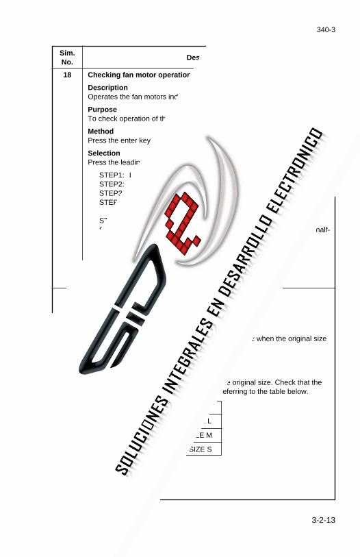
3-2-13
340-3
Sim.No.
Description
18 Checking fan motor operation
DescriptionOperates the fan motors individually.
PurposeTo check operation of the fan motors.
MethodPress the enter key. A step number is shown on the display.
SelectionPress the leading edge margin key to change the step number.
STEP1: LPH fan motors 1, 2 onSTEP2: LPH fan motors 1, 2 half-speedSTEP3: Cooling fan motor full-speedSTEP4: Cooling fan motor half-speed, Right/left fixing fan motors half-
speedSTEP5: Right/left fixing fan motors full-speedSTEP6: Right/left fixing fan motors off, paper conveying fan motor half-
speedSTEP7: Paper conveying fan motor full-speedSTEP8: Paper conveying fan motor off
CompletionPress the stop/clear key.
21 Checking original size detection operation
DescriptionDisplays original size detection action.
PurposeTo check operation of original size switches 1 and 2 when the original sizeis not detected correctly.
Method1. Press the enter key.
2. Slide the original guides according to the original size. Check that theindication on the display is correct by referring to the table below.
CompletionPress the stop/clear key.
Original size Display
B2/24" or larger ORG SIZE L
B2 – B3/24" – 22" ORG SIZE M
A3/18" or smaller ORG SIZE S

3-2-14
340-3
Sim.No.
Description
22 Checking original detection switch operation
DescriptionDisplays the actions of the original leading/trailing edge detection switches.
PurposeTo check the original leading/trailing edge detection switches when theoriginal feed fails.
Method1. Open the original holding section.
2. Press the enter key. “S1 S2” is shown on the display.
3. Turn the original leading edge detection switch on. An asterisk is shownagainst S1 on the display.
4. Turn the original trailing edge detection switch on. An asterisk is shownagainst S2 on the display.
CompletionPress the stop/clear key.
24 Checking original feed motor operation
DescriptionOperates the original feed motor.
PurposeTo check the operation of the original conveying system.
MethodPress the enter key. The following operations take place every 4 seconds.
Original feed motor rotates forwardOriginal feed motor reversesOriginal feed motor off
CompletionPress the stop/clear key.
25 Adjustment for prescan in reduction copy mode
AdjustmentSee page 3-3-30-11.

3-2-15
340-3
Sim.No.
Description
26 Setting delay before original feed start
DescriptionSets the time to turn the original feed clutch on after the original leadingedge detection switch is turned on.
PurposeTo facilitate copying for unaccustomed users by extending the time to startprimary original feed after the insertion of original.
MethodPress the enter key.
SettingSelect the setting with the mode set keys.
Setting description: time from original leading edge detection switch ‘on’ tooriginal feed clutch ‘on’
1: 0.64 sec2: 2 sec3: 3 sec4: 4 sec5: 5 sec
CompletionPress the stop/clear key.

3-2-16
340-3
Sim.No.
Description
31 Ignoring developing control
DescriptionSets whether developing control is ignored or not.
PurposeTo operate the machine with the developing section removed.
MethodPress the enter key.
SettingChoose a setting with the mode set keys.
CompletionPress the stop/clear key.
33 Turning the transfer charger on
DescriptionPerforms transfer charging.
PurposeTo check if transfer charging is performed correctly when a transfer problemoccurs.
MethodPress the enter key. Transfer charging starts.
CompletionPress the stop/clear key. Transfer charging ends.
34 Turning the separation charger on
DescriptionPerforms separation charging.
PurposeTo check if separation charging is performed correctly when a separationproblem occurs.
MethodPress the enter key. Separation charging starts.
CompletionPress the stop/clear key. Separation charging ends.
Display Setting description
1: CANCEL OFF Developing control used
2: CANCEL ON Developing control ignored

3-2-17
340-3
Sim.No.
Description
35 Entering drum surface potential data for black & white mode
DescriptionSets the drum surface potential in black & white (character) mode.
PurposeTo enter the value written on the simulation label after replacing the backupPCB or simulation 70 has been run.
MethodPress the enter key.
SelectionSelect the setting with the leading edge margin key or left margin key. Thecurrent setting value is shown on the display.
SettingChange the setting value with the mode set or numeric keys.
CompletionPress the stop/clear key.
Display Setting description Setting range Default
TRGT Drum surface potential inblack & white (character) 0 – 255 224mode
LPH ON LPH output in black & white(character) mode 0 – 255 18

3-2-18
340-3
Sim.No.
Description
36 Entering drum surface potential data for half-tone mode
DescriptionSets the drum surface potential in half-tone mode.
PurposeTo enter the value written on the simulation label after replacing the backupPCB or simulation 70 has been run.
MethodPress the enter key.
SelectionSelect the setting with the leading edge margin key or left margin key. Thecurrent setting value is shown on the display.
SettingChange the setting value with the mode set or numeric keys.
CompletionPress the stop/clear key.
Display Setting description Setting range Default
TRGT HLF Drum surface potential inhalf-tone mode 0 – 255 191
LPH ON HLF LPH output in half-tonemode 0 – 255 9

3-2-19
340-3
Sim.No.
Description
39 Displaying the thermistor outputs
DescriptionDisplays the detected temperatures of the thermistors.
PurposeTo check the temperatures inside and outside the machine and near thefluorescent lamp.
MethodPress the enter key. The detected temperatures (°C) of the followingthermistors are shown on the display.
CompletionPress the stop/clear key.
Display Description
DTH Dehumidifier thermistor (temperatureinside the machine)
ATMO External temperature thermistor(temperature outside the machine)
LTH Fluorescent lamp thermistor(temperature near the fluorescent lamp)

3-2-20
340-3
Sim.No.
Description
40 Coating the cleaning blade with toner
DescriptionApplies toner to the cleaning blade by coating the drum with toner. Thissimulation can be run after machine stabilization. To run this simulationbefore machine stabilization, run simulation 41 first.
PurposeUsed when replacing the cleaning blade or drum or installing the copier.
MethodPress the enter key. The following operations take place:
Cleaning solenoid turns off.0.1 s later ↓
Developing bias (600 V DC) and drive motor turn on.(Toner is applied to the drum.)
4.5 s later ↓Drive motor turns off
0.5 s later ↓Cleaning solenoid turns on
0.5 s later ↓Drive motor turns on(The blade cleans the toner off the drum, so coating the blade.)
29.5 s later ↓Drive motor, developing bias and cleaning solenoid turn off.
CompletionPress the stop/clear key.
41 Forced stabilization
DescriptionThe copier enters the forced stabilization mode before the fixing section isheated to the stabilization temperature level.
PurposeUsed when setting the initial value of the developer.
MethodPress the enter key. The copier enters the forced stabilization mode and theready lamp lights.
CompletionTurn the main switch off and on to exit the forced stabilization mode.

3-2-21
340-3
Sim.No.
Description
42 Displaying the fixing unit thermistor detection temperatures
DescriptionDisplays detected temperatures of fixing unit thermistors 1 to 4 and theexternal temperature thermistor.
PurposeTo check the fixing temperature when a fixing problem occurs.
Method1. Press the enter key. The current temperatures detected by fixing unit
thermistors 1 to 4 and the external temperature thermistor are shown onthe display in °C.
2. Press the special paper select key to choose the paper type. The fixingtemperature control changes according to the paper type and the currentthermistor detection temperatures are displayed.
Display example
157 157 081 079 025
1 2 3 4 5
CompletionPress the stop/clear key.
Data No. Detection temperature
1 Temperature detected by fixing unit thermistor 1(the temperature around the center of the heat roller)
2 Temperature detected by fixing unit thermistor 2(the temperature at the end of the heat roller)
3 Temperature detected by fixing unit thermistor 3(the temperature around the center of the press roller)
4 Temperature detected by fixing unit thermistor 4(the temperature at the end of the press roller)
5 Temperature detected by external thermistor(temperature outside the machine)

3-2-22
340-3
Sim.No.
Description
44 Turning the cleaning lamps on
DescriptionTurns the pre-charging and post-transfer lamps on.
PurposeTo check the operation of the lamps when an offset occurs.
MethodPress the enter key. The pre-charging and post-transfer lamps turn on.
CompletionPress the stop/clear key. All the components are turned off.
45 Checking cleaning solenoid operation
DescriptionOperates the cleaning solenoid.
PurposeTo check cleaning solenoid operation when an offset occurs.
MethodPress the enter key. The cleaning solenoid turns on.
CompletionPress the stop/clear key. The cleaning solenoid turns off.
46 Setting fixing stabilization at low speed
DescriptionSets the fixing motor control when the fixing temperature falls to 80°C/176°For below.
PurposeTo heat the press roller evenly when copy paper is wrinkled.
MethodPress the enter key. The current temperature is shown on the display.
SettingChange the setting with the mode set keys.
Caution: When 1 is selected, copying is possible even if the surface tem-perature is not correct. However, copying in this condition maylead to image problems. We cannot guarantee the performancesince problems may be caused by such operation.
CompletionPress the stop/clear key.
Display Setting description
1 OFF The fixing motor does not start rotating at low speed.
2 ON The fixing motor rotates at low speed when thefixing temperature falls to 80°C/176°F or below.

3-2-23
340-3
Sim.No.
Description
47 Checking fixing heater operation
DescriptionTurns fixing heaters M and S on.
PurposeTo check the operation of fixing heaters M and S.
MethodPress the enter key. Fixing heaters M and S turn off.
SelectionSelect a heater to be turned on with the leading edge margin key or leftmargin key and then press the enter key. The selected heater turns on.
CompletionPress the stop/clear key to turn the heater off.
48 Checking separation claw solenoid operation
DescriptionOperates the separation claw solenoid.
PurposeTo check the operation of the separation claw solenoid when a separationproblem occurs.
MethodPress the enter key. The separation claw solenoid turns on.
CompletionPress the stop/clear key. The separation claw solenoid turns off.
Display Operation description
HEAT1 DARK Fixing heater M on
HEAT1 LIGHT Fixing heater M on
HEAT2 DARK Fixing heater S on
HEAT2 LIGHT Fixing heater S on

3-2-24
340-3
Sim.No.
Description
50 Turning all the operation unit LEDs on
DescriptionTurns LEDs on the operation panel on.
PurposeTo check the indicators and ready-lamp on the operation panel.
MethodPress the enter key. All the indicators and the ready lamp on the operationpanel turn on.
CompletionPress the stop/clear key. All the indicators and the ready lamp turn off.
53 Adjusting 100% magnification
AdjustmentSee page 3-3-22.
54 Adjusting leading edge registration
AdjustmentSee page 3-3-23.
55 Adjusting synchrocut length (297 mm)
AdjustmentSee page 3-3-6.
56 Adjusting synchrocut length (1189 mm)
AdjustmentSee page 3-3-3.
57 Adjusting the leading edge margin
AdjustmentSee page 3-3-5.
58 Adjusting the trailing edge margin/displayed synchrocut length
AdjustmentSee page 3-3-9, 17.
59 Adjusting the paper cut position for specified length cut mode
AdjustmentSee page 3-3-7.

3-2-25
340-3
Sim.No.
Description
60 Loading developer
DescriptionDetermines the toner control voltage automatically.
PurposeUsed at machine setup and after replacing the developing assembly ordeveloper.
MethodPress the enter key. The drive motor turns on to conduct aging for threeminutes. After the completion of aging, the toner control voltage isautomatically determined and shown on the display. The toner controlvoltage adjusted value set in simulation 63 is reset to zero.
Display example
177 176
1 2
• Pressing the stop/clear key during aging stops the drive motor andinterrupts developer setting.
• Write down the value on the simulation label.
CompletionPress the stop/clear key.
Data No. Display description
1 Toner sensor output value
2 Toner control voltage

3-2-26
340-3
Sim.No.
Description
61 Turning developing bias on
DescriptionOutputs the developing bias.
PurposeTo check if the developing bias is output correctly when image contrast ispoor.
MethodPress the enter key.
SelectionSelect the bias mode with the mode set keys. The developing bias turns onat the value corresponding to the selected bias mode.
CompletionPress the stop/clear key to turn the developing bias off.
Bias mode Developing bias value
BIAS1 –100 V DC
BIAS2 0 V DC
BIAS3 150 V DC
BIAS4 300 V DC
BIAS5 450 V DC
BIAS6 600 V DC
BIAS7 650 V DC

3-2-27
340-3
Sim.No.
Description
63 Checking/changing toner control voltage
DescriptionChecks/sets the toner control voltage value determined automatically insimulation 60.
PurposeUsed after replacing the backup PCB.
MethodPress the enter key.
SelectionChange the setting by pressing leading edge margin key or left margin key.
Indication 1S: Toner control voltage value (the same value as simulation 60)ON: Level where the toner feed motor is turned onOFF: Level where the toner feed motor is turned off
Indication 2TE: Toner empty levelTEHI: Copying impossible level
Indication 3Adjusted value of the toner control voltage(The toner control voltage set in simulation 60 can be changed.)
SettingChange the value of indication 3 using the mode set keys.
• Setting range: ±128 (as long as the data remains above 0)Default: 0
• The values for indications 1 and 2 automatically change corresponding tothe value for indication 3. However, the value for S in indication 1 does notchange.
• The value for indication 3 is reset to zero after simulation 60 is run.
CompletionPress the stop/clear key.
3-2-28
340-3
Sim.No.
Description
64 Checking toner feed motor operation
DescriptionCarries out toner replenishment.
PurposeTo check the toner feed motor operation when a toner replenishmentproblem occurs.
MethodPress the enter key. The toner feed motor turns on for 5 s and toner is fed.
• To interrupt the toner feed motor, press the stop/clear key.
CompletionPress the stop/clear key.
65 Displaying toner sensor output
DescriptionDisplays the toner sensor output and temperature detected by thedeveloping unit thermistor.
PurposeTo check the temperature compensation of the toner sensor output.
MethodPress the enter key. The following data is shown on the display.
Display example
167 171 026
1 2 3
Note: The toner sensor output value is displayed as a decimal. Multiplying itby 0.02 gives the toner sensor output voltage.
e.g. Toner sensor output value is displayed as 185:Toner sensor output voltage = 185 × 0.02 = 3.7 (V)
CompletionPress the stop/clear key.
Data No. Display description
1 Toner sensor output value
2 Toner sensor output value after temperature compensation
3 Temperature detected by the developing unit thermistor (°C)

3-2-29
340-3
Sim.No.
Description
66 Entering toner sensor control level/copy count
DescriptionChecks/sets the toner control voltage and copy count which are determinedautomatically in simulation 60.
PurposeTo set the toner sensor control level and copy count to the values setautomatically in simulation 60 after the backup PCB has been replaced andsimulation 70 has been run.
MethodPress the enter key.
SelectionSelect the setting with the leading edge margin key or left margin key. Thecurrent setting value is shown on the display.
SettingChange the setting value with the mode set keys or numeric keys.
CompletionPress the stop/clear key.
67 Selecting operation under the empty toner condition
DescriptionSets whether to enable continuous copying after toner empty is detected.
PurposeSet according to user request.
MethodPress the enter key. The current setting value is shown on the display.
SelectionSelect the setting value with the mode set keys.
CompletionPress the stop/clear key.
Display Setting description
1: SINGLE Single copying only
2: CONTINUATION Continuous copying available
Display Setting Setting range
1: START Toner control voltage 0 – 255
2: COUNTER Copy count 0 – 12000 (m)

3-2-30
340-4
Sim.No.
Description
70 Initializing backup memory 1
DescriptionInitializes the contents of the backup memory.
PurposeUsed after replacing the backup PCB.
Method1. Press the enter key. The display changes from “INITIALIZING ON” to
“INITIALIZING OK”.
2. Turn the main switch off and on. The contents of the following itemshave now been initialized.
Sim No. Contents Default
25 Adjustment for prescan in reduction copy mode 026 Setting delay before original feed start 1: 0.64 sec31 Ignoring developing control 1: CANCEL
OFF35 Entering drum surface potential data for
black & white modeTRGT 224LPH ON 18
36 Entering drum surface potential data forhalf-tone mode
TRGT HLF 191LPH ON HLF 9
46 Setting fixing stabilization at low speed 2: ON53 Adjusting 100% magnification 054 Adjusting leading edge registration 055 Adjusting synchrocut length (297 mm) 056 Adjusting synchrocut length (1189 mm)
Conveying speed at the 1st roll unit(plain paper) 0Conveying speed at the 1st roll unit(tracing paper) 0Conveying speed at the 1st roll unit (film) 0Conveying speed at the 3rd roll unit(plain paper) 0Conveying speed at the 3rd roll unit(tracing paper) 0Conveying speed at the 3rd roll unit (film) 0
57 Adjusting the leading edge marginRoll unit 0Bypass table 0

3-2-31
340-4
Sim.No.
Description
58 Adjusting the trailing edge margin/displayedsynchrocut length
Trailing edge margin 0Displayed synchrocut length 0
59 Adjusting the paper cut position for specifiedlength cut mode
Short, 1st roll unit (plain paper) 0Short, 1st roll unit (tracing paper) 0Short, 1st roll unit (film) 0Short, 3rd roll unit (plain paper) 0Short, 3rd roll unit (tracing paper) 0Short, 3rd roll unit (film) 0Long, 1st roll unit (plain paper) 0Long, 1st roll unit (tracing paper) 0Long, 1st roll unit (film) 0Long, 3rd roll unit (plain paper) 0Long, 3rd roll unit (tracing paper) 0Long, 3rd roll unit (film) 0
63 Checking/changing toner control voltageAdjusted value of the toner control voltage 0
66 Entering toner sensor control level/copy countSTART 155COUNTER 0
67 Selecting operations under empty toner condition 1: SINGLE71 Selecting the maintenance cycle 1: OFF75 Entering the service telephone No. Cleared80 Switching the counter counting units 2: 1 m81 Selecting the language 1: JAPANESE82 Selecting between key counter/card KEY-CARD: 083 Selecting between metric/inch 1: CENCH84 Selecting the No. of exposure steps 1: 13 STEPS86 Switching the fixing temperature 1: JPN87 Disabling cancellation of auto shutoff function 1: ON89 Setting optional roll unit 1: NO CON-
NECT92 Setting potential correction intervals 3: ON (20 m)94 Setting the maximum copy length for multiple ORG MAX:
copy mode 140095 Setting the maximum copy length for roll/ PAPER MAX:
bypass mode 5000
Sim No. Contents Default70(cont.)

3-2-32
340-4
Sim.No.
Description
Sim No. Contents Default
96 Selecting the action after paper empty detectionPlain paper 10 sTracing paper 10 sFilm 1 s
97 Switching between front and rear ejection oforiginals
ORG PSTN (S) 1: EJECTORG PSTN (C) 2: RETURN
98 Selecting the copy count timing MODE 1115 Selecting the connection to the interface
controller 1116 Setting the time to return from the offline
condition 5117 Adjusting the leading edge registration
(when connected to the interface controller) 0132 Adjusting optical axis 0133 Adjusting the image width in the main scanning
direction 0140 Adjusting exposure amount
EXP (PLAIN) 4EXP (DARK) 4EXP (LIGHT) 4EXP (HALF PLAIN) 4EXP (HALF DARK) 4EXP (HALF LIGHT BD) 4EXP (HALF LIGHT BL) 5
141 Half-tone image quality (dark/light)HALF D 0HALF L BD 3
142 Adjusting AE optimum levelPOINT (PLAIN) 4POINT (DARK) 1POINT (LIGHT) 8MAX (PLAIN) 12MAX (DARK) 12MAX (LIGHT) 18
143 Switching filter modes MODE 1
70(cont.)

3-2-33
340-4
Sim.No.
Description
CompletionPress the stop/clear key.
ImportantDo NOT forget to run simulation 120 after simulation 70.
70(cont.)
Sim No. Contents Default
144 Adjusting filter gainCHARACTER 1.0HALF LIGHT BD 0.5HALF LIGHT BL 0.6
145 Setting AE fine adjustment intervals 3153 Selecting current correction value MODE: 00160 Adjusting base 4 output density
DENSITY 2 0DENSITY 3 0
161 Adjusting thresholds (central exposure level)THLD BW 0THLD HLF 1 0THLD HLF 2 0THLD HLF 3 0
163 Adjusting Exp. 1.0 thresholdTHLD BW (1.0) 0THLD HLF (1.0) 0
164 Adjusting Exp. 7.0 thresholdTHLD BW (7.0) 0THLD HLF (7.0) 0
165 Setting the memory unit connection 1: NO CON-NECT
166 Selecting display of the “Output?” screen after 1: DISP ONrestart
167 Setting the AE scan 0168 Setting the maximum number of continuous
copies 1178 Selecting memory output mode 2
3-2-34
340-4
Sim.No.
Description
71 Selecting the maintenance cycle
DescriptionWhen the maintenance count reaches the value set in simulation 71, themaintenance time indication is shown.
PurposeUsed after replacing the backup PCB.
MethodPress the enter key. The current maintenance cycle is shown on thedisplay.
SelectionChange the setting with the mode set keys.Contents of the modes:
MAINTENANCE1: OFFMAINTENANCE2: 750 mMAINTENANCE3: 1500 mMAINTENANCE4: 3000 mMAINTENANCE5: 5000 ft
• If set to “MAINTENANCE1: OFF” the maintenance time indication will notbe shown.
CompletionPress the stop/clear key.
72 Setting/clearing the maintenance count
DescriptionChecks/resets the maintenance count.
PurposeUsed when the maintenance time indication is shown.
MethodPress the enter key. The current maintenance count is shown on thedisplay.
Setting1. Change the setting with the mode set keys or numeric keys.
2. Press the enter key.
Resetting the maintenance count1. Enter “0” with the numeric key.
• If the message “Maintenance due/TIME FOR MAINTENANCE” isshown on the display, it goes off.
2. Press the enter key.
CompletionPress the stop/clear key.

3-2-35
340-4
Sim.No.
Description
73 Displaying/clearing total paper feed count
DescriptionChecks/resets the total paper feed count.
PurposeTo check the replacement time of the maintenance parts.
MethodPress the enter key. The number of copies made since the last countsetting to the present is shown on the display.
Display example
TOTAL 1580
ResettingEnter “0000” with the numeric key and then press the enter key. Resettingof the total count is completed.
CompletionPress the stop/clear key.

3-2-36
340-4
Sim.No.
Description
74 Displaying/clearing the jam counts by paper source
DescriptionChecking/resetting the jam counts.
PurposeTo check the replacement time of the maintenance parts.
MethodPress the enter key. Jam locations and jamming frequency are displayed.
SelectionSelect the jam location which should be reset by pressing the leading edgemargin (up) key or left margin (down) key.
ResettingEnter “0” with the numeric key and then press the enter key. Resetting ofthe jam count is completed.
CompletionPress the stop/clear key.
Display Location of jams JAM code
1: BYPASS JAM Bypass J-01
2: ROLL-U JAM 1st roll unit J-02
3: ROLL-M JAM 2nd roll unit J-03
4: ROLL-L JAM 3rd roll unit J-04
5: ORIGINAL JAM Original conveying section J-05
6: FEEDING JAM Inside the copier J-06

3-2-37
340-4
Sim.No.
Description
75 Entering the service telephone No.
DescriptionSets the telephone number to be shown on the service call code display.
PurposeUsed after replacing the backup PCB.
MethodPress the enter key.
Setting1. Enter the telephone number with the following keys.
2. Press the enter key.
CompletionPress the stop/clear key.
Keys to be pressedCharacters and
symbols
Numeric keys 0 – 9
Special paper select key —
Image process select key /
Original contrast key (
Auto/manual contrast select key )
Copy contrast key (dark) ∗
Copy contrast key (light) #
Decimal point Space

3-2-38
340-4
Sim.No.
Description
76 Displaying/clearing paper feed count by paper source
DescriptionChecks/resets the total count value for each paper source.
PurposeTo check the replacement time of the maintenance parts.
MethodPress the enter key. The paper feed count for the currently selected papersource is shown on the display.
SelectionSelect the paper source to be checked by pressing the leading edge margin(up) key or left margin (down) key.
• The indicator corresponding to the selected paper source lights and thecurrent paper feed count is shown.
Resetting1. Enter “0” with the numeric key.
2. Press the enter key.
CompletionPress the stop/clear key.
Display Paper source
1: BYPASS Bypass section
2: ROLL-U 1st roll unit
3: ROLL-M 2nd roll unit
4: ROLL-L 3rd roll unit (optional)

3-2-39
340-4
Sim.No.
Description
77 Clearing the counts
DescriptionClears all the counts at one time.
PurposeTo be run during full maintenance.
MethodPress the enter key. “FINISHED” is shown on the message display and allthe counts shown below and the developing count are reset to zero.
CompletionPress the stop/clear key.
Sim. No. Count
72 Maintenance count
73 Total count
74 Jam counts by paper source
76 Total counts by paper source

3-2-40
340-4
Sim.No.
Description
78 Displaying set data
DescriptionDisplays data settings of the simulation items.
PurposeTo check data settings.
MethodPress the enter key.
Selection1. Select the simulation No. to be checked with the leading edge margin
key and left margin key.
2. Select the type of data to be checked with the mode set keys.
The following data can be checked by this simulation.
CompletionPress the stop/clear key.
Sim. No. Data
30* Setting drum surface potential 132* Setting drum surface potential 253 Adjusting 100% magnification54 Adjusting leading edge registration55 Adjusting synchrocut length (297 mm)56 Adjusting synchrocut length (1189 mm)57 Adjusting the leading edge margin58 Adjusting the trailing edge margin/displayed synchrocut length59 Adjusting the paper cut position for specified length cut mode60 Loading developer
140 Adjusting exposure amount141 Half-tone image quality (dark/light)142 Adjusting AE optimum level153 Selecting current correction value
*Simulations 30 and 32 are for line use only.

3-2-41
340-4
Sim.No.
Description
79 Specifying addresses/displaying data
DescriptionDisplaying internal data.
PurposeNo need to run this simulation during maintenance.
MethodPress the enter key. The address No. for internal data is shown as sixbinary digits and the contents are displayed in hexadecimal.
Display example
000000 00C0
Specifying addressEnter the address by pressing numeric keys 1 to 6.
CompletionPress the stop/clear key.
80 Switching the counter counting units
DescriptionChanges the units used by the total counter and key counter.
PurposeTo change the counter counting units according to the paper consumption.
MethodPress the enter key.
SettingChange the counting units with the mode set keys.
1: 0.1 m2: 1 m
With the setting at 1, the total counter and key counter count up every 0.1 mof paper; with the setting at 2, they count up every 1 m.
CompletionPress the stop/clear key.

3-2-42
340-4
Sim.No.
Description
81 Selecting the language
DescriptionChanges the language of the messages.
PurposeTo be set according to user request.
MethodPress the enter key. The current language is shown on the display.
SelectionSelect one of the following languages with the mode set keys:
CompletionPress the stop/clear key.
82 Selecting between key counter/card
DescriptionSets the installation of the key counter/card.
PurposeUsed after the optional key counter has been installed.
MethodPress the enter key.
SettingSelect “KEY-CARD: 0” with the mode set keys.
CompletionPress the stop/clear key.
1 Japanese
2 English (UK)
3 German
4 French
5 Spanish
6 Dutch
7 Italian
8 English (USA)

3-2-43
340-4
Sim.No.
Description
83 Selecting between metric/inch
DescriptionSets the specification of the copier to metric or inch.
PurposeUsed after replacing the backup PCB.
MethodPress the enter key. The current setting is shown on the display.
SettingChange the setting with the mode set keys.
Setting description1: CENCH2: INCH
CompletionPress the stop/clear key.
84 Selecting the No. of exposure steps
DescriptionSets the number of exposure steps.
PurposeTo be set according to user request.
MethodPress the enter key. The current setting is shown on the display.
SettingChange the setting with the mode set keys.
Setting description1: 13 STEPS2: 7 STEPS
CompletionPress the stop/clear key.

3-2-44
340-4
Sim.No.
Description
85 Initializing backup memory 2
DescriptionInitializes the backup memory according to the destination.
PurposeUsed after replacing the backup PCB.
MethodPress the enter key.
SelectionSelect the destination with the mode set keys.
Initialization1. Press the enter key. The display changes from “INITIALIZING ON” to
“INITIALIZING OK”.
2. Turn the main switch off and on. The following items and the user-setcontents are initialized to the values corresponding to the destination:
CompletionPress the stop/clear key.
Display Destination
1. JPN Specification for Japan
2. OTHERS Specifications for other countries
Sim. No. ContentsDefaults
JPN OTHERS
94 Setting the maximum copy length formultiple copy mode
1400 mm 1400 mm
95 Setting the maximum copy length forroll/bypass mode
5000 mm 5000 mm
96 Selecting the action after paper empty 10 s for 1 s fordetection plain paper plain paper
3-2-45
340-4
Sim.No.
Description
86 Switching the fixing temperature
DescriptionSets the secondary fixing temperature according to the destination.
PurposeUsed after replacing the backup PCB.
MethodPress the enter key. The current setting is shown on the display.
SettingChange the setting with the mode set keys.
Setting description1: JPN (100 V areas)2: OTHERS (120 V, 200 V areas)
CompletionPress the stop/clear key.
87 Disabling cancellation of auto shutoff function
DescriptionSets whether the auto shutoff function is used.
PurposeTo be set according to user request.
MethodPress the enter key. The current setting is shown on the display.
SettingChange the setting with the mode set keys.
Default 1: ON
To cancel the auto shutoff function, change the setting to OFF and select“– – –” for the time setting.
CompletionPress the stop/clear key.
Display Setting description
1: ON Auto shutoff function used
2: OFF Auto shutoff function not used
3-2-46
340-4
Sim.No.
Description
89 Setting optional roll unit
DescriptionSets the installation of the 3rd roll unit.
PurposeTo be set after the optional 3rd roll unit is installed.
MethodPress the enter key. The current setting is shown on the display.
SettingChange the setting with the mode set keys.
Default 1: NO CONNECT
CompletionPress the stop/clear key.
92 Setting potential correction intervals
DescriptionSets the interval for the drum potential correction.
PurposeTo set the intervals so that the drum potential is corrected whenever thebackground becomes visible due to the decline in drum quality.
MethodPress the enter key. The current setting is shown on the display.
SettingChange the setting with the mode set keys.
Default 3: ON (20 m)
CompletionPress the stop/clear key.
Display Setting description
1: NO CONNECT 3rd roll unit not installed
2: CONNECT 3rd roll unit installed
Display Setting description
1: OFF Correct potential during stabilization only
2: ON Correct potential every copy
3: ON (20 m) Correct potential every 20 m

3-2-47
340-4
Sim.No.
Description
94 Setting the maximum copy length for multiple copy mode
DescriptionSets the maximum copy length for multiple copy mode.
PurposeTo be set according to user request.
MethodPress the enter key. The maximum copy length for multiple copy mode isshown on the display.
Display example
ORG MAX: 1500
SettingChange the setting with the mode set keys. The setting can be changed insteps of 100 mm between 1400 and 5000 mm.
CompletionPress the stop/clear key.
95 Setting the maximum copy length for roll/bypass mode
DescriptionSets the maximum copy length for roll/bypass mode.
PurposeTo be set according to user request.
MethodPress the enter key. The maximum copy length for roll/bypass mode isshown on the display.
Display example
PAPER MAX: 1500
SettingChange the setting with the mode set keys. The setting can be changed insteps of 100 mm between 5000 and 9900 mm.
CompletionPress the stop/clear key.

3-2-48
340-4
Sim.No.
Description
96 Selecting the action after paper empty detection
DescriptionSets the time before the paper empty detection function is activated.
PurposeTo be set depending on the type of roll paper in each paper source.
MethodPress the enter key.
SelectionSelect the type of paper to be set with the leading edge margin key or leftmargin key. The setting value for the selected paper is shown on thedisplay.
SettingChange the setting value with the mode set keys.
CompletionPress the stop/clear key.
Display Type of roll paper
1: NORMAL Plain paper
2: VELLUM Tracing paper
3: FILM Film
Settingvalue
Setting description
10 s With roll paper whose end is glued to the core
1 s With roll paper whose end is not glued to the core

3-2-49
340-4
Sim.No.
Description
97 Switching between front and rear ejection of originals
DescriptionSwitches the ejection direction of originals after copying.
PurposeTo be set according to user request.
MethodPress the enter key.
SelectionSelect the copy mode to be set with the leading edge margin key and leftmargin key. The setting value of the selected mode is shown on the display.
ORG PSTN (S): Single copy modeORG PSTN (C): Continuous copy mode
SettingChange the settings with the mode set keys.
CompletionPress the stop/clear key.
98 Selecting the copy count timing
DescriptionChanges the counting timing of the total counter.
PurposeSet to MODE 1 if paper jams should be included in the total count.
MethodPress the enter key. The current counting timing mode is shown on thedisplay.
SettingChange the setting with the mode set keys.
CompletionPress the stop/clear key.
Setting Setting description
1: EJECT The original is ejected to the rear
2: RETURN The original returns to the front
Display Setting description
MODE 1 During paper feed
MODE 2 After paper ejection
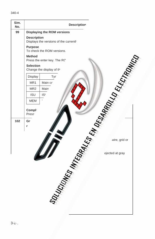
3-2-50
340-4
Sim.No.
Description
99 Displaying the ROM versions
DescriptionDisplays the versions of the currently installed ROMs.
PurposeTo check the ROM versions.
MethodPress the enter key. The ROM versions are shown on the display.
SelectionChange the display of the ROM versions with the mode set keys.
CompletionPress the stop/clear key.
102 Gray output
DescriptionOutputs a gray test pattern.
PurposeTo check for a main PCB or LPH problem, dirty main charger wire, grid orhousing or drum problem.
MethodPress the enter key. A test pattern copy 594 mm long is ejected at graylevel 8.
Figure 3-2-1
CompletionPress the stop/clear key.
Display Type of ROM
MR1 Main control ROM 1
MR2 Main control ROM 2
ISU ISU CPU
MEM Memory unit

3-2-51
340-4
Sim.No.
Description
103 32-gradation output
DescriptionOutputs a 32-gradation test pattern with the LPH current corrected.
PurposeTo check for an LPH problem, dirty main charger wire, grid or housing ordrum problem.
See page 3-3-18.
MethodPress the enter key. A test pattern copy in 32 gradation levels is ejected.
Figure 3-2-2
InterruptionPress the job stop/roll cut key. The paper being printed is cut at themidpoint, ending the operation.
CompletionPress the stop/clear key.

3-2-52
340-4
Sim.No.
Description
104 32-gradation output (without compensation)
DescriptionOutputs a 32-gradation test pattern without correcting the LPH current.
PurposeTo check if the LPH current correction ROM is correctly installed to the mainPCB.
MethodPress the enter key. A test pattern copy in 32 gradation levels is ejected asin simulation 103.
Figure 3-2-3
• When white stripes appear at 8-mm intervals in simulation 104 as shownabove while the correct image is obtained during simulation 103, the LPHcurrent correction ROM is judged to be correctly installed.
CompletionPress the stop/clear key.

3-2-53
340-4
Sim.No.
Description
109 Setting the controller type
DescriptionSets the type of CAD controller to be used.
PurposeTo be set after installation of the interface controller.
MethodPress the enter key.
SelectionSelect the type of CAD controller with the mode set keys.
Default 1. TYPE A
CompletionPress the stop/clear key.
Display Setting description
1. TYPE A A controller other than OEM 1 is used with the copier.(The copier automatically enters on-line mode when theauto clear time passes after the completion of copying.)
2. TYPE B1 An OEM 1 controller is used with the copier. (The copierautomatically enters on-line mode when the auto cleartime minus 10 s passes after the completion of copying.)
3. TYPE B2 An OEM 1 controller is used with an OEM 1 copier(The copier automatically enters on-line mode 5 s afterthe completion of copying.)

3-2-54
340-4
Sim.No.
Description
110 Checking fluorescent lamp operation
DescriptionLights the fluorescent lamp.
PurposeTo check the fluorescent lamp operation.
MethodPress the enter key. The fluorescent lamp lights and the display shows thefollowing data.
Display example
1: 90 120
1 2
CompletionPress the stop/clear key.
Data No. Contents
1 Standard fluorescent lamp light amount
2 Current fluorescent lamp light amount

3-2-55
340-4
Sim.No.
Description
111 Checking shading compensation operation
DescriptionPerforms shading compensation and shows CIS channel data.
PurposeTo check respective channel data when solid black areas are too thin orwhite stripes appear on the copy image.
MethodPress the enter key. After shading compensation is completed, channeldata is shown on the display.
SelectionChannel data is displayed three channels at a time. To see the next three,press the leading edge margin key or the left margin key.
Display example
1: 0 2: 1 3: 1
↓ ↑
4: 0 5: 200 6: 199
↓ ↑
7: 204 8: 203
The following contents are shown:
• When the data with the lamp off is around 0 and that with the lamp on isaround 200, shading compensation is judged to be normal.
CompletionPress the stop/clear key.
Data for sensors ch1 to ch4 with lamp off 1: 2: 3: 4:
Data for sensors ch1 to ch4 with lamp on 5: 6: 7: 8:

3-2-56
340-4
Sim.No.
Description
Data for sensors ch1 to ch4 with lamp off 1: 3: 5: 7:
Data for sensors ch1 to ch4 with lamp on 2: 4: 6: 8:
112 Checking AGC processing operation
DescriptionPerforms AGC processing and shows data of the CIS channels.
PurposeTo check for an AGC error during A-D conversion.
MethodPress the enter key. After AGC processing is completed, the display showsthe mean values for individual channels.
SelectionChannel data is displayed three channels at a time. To see the next three,press the leading edge margin key or the left margin key.
Display example
1: 0 2: 1 3: 1
↓ ↑
4: 0 5: 200 6: 199
↓ ↑
7: 204 8: 203
The following contents are shown:
• When the data with the lamp off is around 0 and that with the lamp on isaround 200, AGC processing is judged to be normal.
CompletionPress the stop/clear key.
113 Setting the shading mode
AdjustmentSee page 3-3-30-12.

3-2-57
340-4
Sim.No.
Description
115 Selecting the connection to the interface controller
DescriptionSelects the connection to the interface controller.
PurposeTo be run after an interface controller is installed.
MethodPress the enter key. The current setting is shown on the display.
SelectionChange the setting with the mode set keys.
1: Interface controller not connected2: Interface controller connected
CompletionPress the stop/clear key.
116 Setting the time to return from the offline condition
DescriptionSets the time to automatically return to on-line mode after the completion ofcopying (completion of key operation on the operation panel).
PurposeTo be set according to user request.
MethodPress the enter key. The current setting is shown on the display.
SelectionChange the setting with the mode set keys.
1: 5 s2: 10 s3: 30 s
CompletionPress the stop/clear key.
117 Adjusting the leading edge registration (when connected to theinterface controller)
AdjustmentSee page 3-3-30-13.

3-2-58
340-4
Sim.No.
Description
120 Adjusting γ correction
DescriptionPerforms γ correction.
PurposeUsed after replacing the backup PCB, ISU PCB or CIS, or after runningsimulation 70 or 121. Be sure to clean the contact glass and the middleupper original rollers before running this simulation.
MethodPress the enter key. The following operations are carried out.
DATA TRANSFERING: data transferAGC ON: AGC processingSHADING: shading compensationDATA PROCESSING: data processing
121 Adjusting gain
DescriptionAdjusts the analog voltage for A-D conversion during original scanning.
PurposeUsed after replacing the ISU PCB. Always run simulation 120 after thissimulation.
MethodPress enter key. The mean gain after shading compensation is shown foreach channel.
Display example
1: 187 2: 211 3: 196 4: 200
After replacing the ISU PCB, adjust VR1, VR3, VR4 and VR5 on the newISU PCB to set the values to 205 ± 20, ensuring that the difference betweenthe maximum and minimum values is 20 or less.
• Setting examples
CompletionPress the stop/clear key.
Channel ch1 (VR3) ch2 (VR1) ch3 (VR5) ch4 (VR4)
Good example 200 205 210 215
Bad example 190 200 230 220

3-2-59
340-4
Sim.No.
Description
132 Adjusting optical axis
AdjustmentSee page 3-3-30-9.
133 Adjusting the image width in the main scanning direction
AdjustmentSee page 3-3-30-10.
140 Adjusting exposure amount
DescriptionSets the exposure amounts for the respective original modes.
PurposeUsed after cleaning or replacing the fluorescent lamp or contact glass.
AdjustmentSee page 3-3-24.
MethodPress the enter key. The current exposure setting is shown on the display.
• The following data (data No., original and exposure setting) can be shownby pressing the original contrast key or auto/manual contrast select key.
SettingChange the exposure setting with the mode set keys.
CompletionPress the stop/clear key.
Data No. Original Exposure setting
1 EXP (PLAIN) For a normal original
2 EXP (DARK) For a dark original
3 EXP (LIGHT) For a light original
4 EXP (HALF PLAIN) For a normal original in half-tone mode
5 EXP (HALF DARK) For a dark original in half-tone mode
6 EXP (HALF LIGHT BD) For a light original (making backgrounddarker)
EXP (HALF LIGHT BL) For a light original (making backgroundlighter)

3-2-60
340-4
Sim.No.
Description
141 Adjusting half-tone image quality
AdjustmentSee page 3-3-26.
142 Adjusting AE optimum level
AdjustmentSee page 3-3-25.
143 Switching filter modes
DescriptionSwitches the contrast for copying letters.
PurposeTo be set according to user request.
AdjustmentSee page 3-3-27.
MethodPress the enter key. The current filter mode is shown on the display.
SelectionChange the setting with the mode set keys. The following modes areavailable.
MODE 1: Normal original (to decrease moiré)
MODE 2: Map original (to copy letters clearly)
Figure 3-2-4
CompletionPress the stop/clear key.

3-2-61
340-4
Sim.No.
Description
144 Adjusting filter gain
AdjustmentSee page 3-3-27.
145 Setting AE fine adjustment intervals
AdjustmentSee page 3-3-25-2.
153 Selecting current correction value
DescriptionPerforms current correction so that the currents of individual LEDsconstituting the LPH are uniform and the gray output during simulation 102is even.
PurposeTo be used after the LPH has been replaced.
MethodPress the enter key. The current LPH current correction mode No. is shownon the display.
Setting1. Change the setting with the mode set keys in the range 00 to 07.
2. Press the enter key. Current correction is conducted.
CompletionPress the stop/clear key.
158 Adjusting focus
AdjustmentSee page 3-3-28.

3-2-62
340-4
Sim.No.
Description
159 Solid black test pattern output
DescriptionOutputs a solid black test pattern.
PurposeTo check for a problem on the main PCB when an image problem occurs.
MethodPress the enter key. A 594-mm-long test pattern for solid black adjustmentis produced.
Figure 3-2-5
• If the correct image is output during simulations 102 and 158 but is notoutput during simulation 159, the main PCB is judged to have a problem.
Figure 3-2-6 Problem-detecting simulations
CompletionPress the stop/clear key.
160 Adjusting base 4 output density
See the memory unit service manual.
161 Adjusting thresholds (central exposure level)
See the memory unit service manual.
162 Adjusting base 4 thresholds simultaneously
See the memory unit service manual.
163 Adjusting Exp. 1.0 threshold
See the memory unit service manual.
CIS
ISUPCB MPCB LPH
Data flow
Sim 159 Sim 102Sim 158

3-2-63
340-4
Sim.No.
Description
164 Adjusting Exp. 7.0 threshold
See the memory unit service manual.
165 Setting the memory unit connection
See the memory unit service manual.
166 Selecting display of the “Output?” screen after restart
See the memory unit service manual.
167 Setting the AE scan
See the memory unit service manual.
168 Setting the maximum number of continuous copies
See the memory unit service manual.
170 Checking the memory unit DRAM
See the memory unit service manual.
172 Checking the memory unit HDD page management area
See the memory unit service manual.
173 Formatting the memory unit HDD
See the memory unit service manual.
174 Cleaning programs 6 to 10
See the memory unit service manual.
175 Restoring programs 6 to 10
See the memory unit service manual.
176 Memory unit problem history
See the memory unit service manual.
177 Clearing the memory unit problem history
See the memory unit service manual.
178 Selecting memory output mode
See the memory unit service manual.
179 Checking the memory unit connection
See the memory unit service manual.

1-1-21
340-4
CONTENTS
3-3 Assembly and Disassembly
3-3-1 Cautions during disassembly and assembly ....................................... 3-3-1(1) Caution ........................................................................................ 3-3-1(2) Method of executing simulation ................................................... 3-3-2
3-3-2 Paper feed section .............................................................................. 3-3-3(1) Adjustment of 1189 mm synchro cut (adjustment of
paper feed motor speed) ............................................................. 3-3-3(2) Leading edge margin adjustment ................................................ 3-3-5(3) Adjustment of 297 mm synchro cut ............................................. 3-3-6(4) Adjustment of paper cutting position when the paper length
is specified ................................................................................... 3-3-7(5) Adjustment of displayed synchro cut length ................................ 3-3-9(6) Attachment and removal of the roll paper feed lower roller A .... 3-3-9-1(7) Attachment and removal of the roll paper conveying rear
roller B (for 2nd roll unit) ........................................................... 3-3-9-3(8) Attachment and removal of the roll paper conveying rear
roller B (for optional 3rd roll unit) .............................................. 3-3-9-5(9) Attachment and removal of the bypass feed roller ................... 3-3-9-6
(10) Attachment and removal of the roll paper conveying rearroller A ...................................................................................... 3-3-9-8
3-3-3 Main charger section ......................................................................... 3-3-10(1) Replacing the drum ................................................................... 3-3-10
(1-1) Cleaning the drum electrodes ...................................... 3-3-12-1(2) Cleaning the drum ..................................................................... 3-3-13(3) Changing the charger wire ........................................................ 3-3-14(4) Adjustment of trailing edge margin ............................................ 3-3-17(5) Checking drum surface potential ............................................... 3-3-18
3-3-4 Exposure and original feed section ................................................... 3-3-19(1) Attachment and removal of fluorescent lamp ............................ 3-3-19(2) Adjustment of 100% magnification ............................................ 3-3-22(3) Adjustment of leading edge registration .................................... 3-3-23(4) Adjustment of exposure amount ................................................ 3-3-24(5) Half tone mode image quality adjustment ................................. 3-3-26(6) Image contrast adjustment (adjustment of filter gain) ............... 3-3-27(7) Image focus adjustment (LPH height adjustment) .................... 3-3-28(8) Replacement of the ISU PCB .................................................... 3-3-30(9) Replacing the LED printhead and LPHROM PCB.................. 3-3-30-1
(10) Cleaning the LED printhead ................................................... 3-3-30-4(11) Replacement of the contact image sensor ............................. 3-3-30-5(12) Adjustment of optical axis ....................................................... 3-3-30-9(13) Adjustment of the image width in the main scanning
direction ................................................................................ 3-3-30-10(14) Adjustment for prescan in reduction copy mode .................. 3-3-30-11(15) Setting the shading mode ..................................................... 3-3-30-12(16) Adjustment of leading edge registration (when connected
to the interface controller) ..................................................... 3-3-30-13

1-1-22
340-4
3-3-5 Developing section ............................................................................ 3-3-31(1) Changing developer .................................................................. 3-3-31(2) Adjustment of doctor blade: reference ...................................... 3-3-33(3) Adjustment of position for magnetic brush: reference ............... 3-3-35(4) Replacement of the lower developing seal ................................ 3-3-36
3-3-6 Transfer/separation section .............................................................. 3-3-37(1) Replacement of charger wire .................................................... 3-3-37(2) Replacement of transfer wire .................................................... 3-3-40
3-3-7 Cleaning section ............................................................................... 3-3-42(1) Attachment and removal of the cleaning blade ......................... 3-3-42(2) Attachment and removal of lower cleaning blade ...................... 3-3-45(3) Attachment and removal of cleaning fur brush .......................... 3-3-46(4) Attachment and removal of separation claw ............................. 3-3-47
3-3-8 Fixing section .................................................................................... 3-3-48(1) Attachment and removal of fixing heaters M and S ................... 3-3-48(2) Attachment and removal of heat roller ...................................... 3-3-49(3) Attachment and removal of the press roller ............................... 3-3-52(4) Attachment and removal of oil roller .......................................... 3-3-53(5) Attachment and removal of fixing unit thermistors 1 and 2 ....... 3-3-56(6) Attachment and removal of fixing unit thermal switches
1 and 2 ...................................................................................... 3-3-57(7) Attachment and removal of fixing unit thermistors 3 and 4 ....... 3-3-58(8) Attachment and removal of the external temperature
thermistor .................................................................................. 3-3-593-3-9 Other sections ................................................................................... 3-3-60
(1) Adjusting the tension of paper feed section drive belt 1 ............ 3-3-60(2) Adjusting the tension of paper feed section drive belt 2 ............ 3-3-61(3) Adjusting the tension of the cutter drive belt ............................. 3-3-62(4) Adjusting the tension of original feed drive belt 1 ...................... 3-3-63
(4-1) Adjusting the tension of the developing drive belt ....... 3-3-63-1(5) Attachment and removal of ozone filter ..................................... 3-3-64

340
3-3-1
3-3-1 Cautions during disassembly and assembly
(1) Caution• When carrying out disassembly, be sure to turn the main switch off and pull out the power
cord before starting.• When handling PCBs avoid touching PCB connectors with the bare hands or scratching
equipment.• When ICs are used on PCBs, do not touch the board with the bare hands or with objects
charged with static electricity.• When replacing the fixing unit thermal switches (thermostats), be sure to use the specified
part. If a simple wire is used instead, damage to the machine may occur.• Use one of the testers shown below when measuring voltage:
• HIOKI 3200• SANWA MD-180C• SANWA YX-360TR• BECKMAN TECH300• BECKMAN 3030: Possible to measure RMS values• BECKMAN 330: Possible to measure RMS values• BECKMAN DM45• BECKMAN DM850: Possible to measure RMS values• FLUKE 8060A: Possible to measure RMS values• ARLEC DMM1050• ARLEC YF1030C
• Originals used.1. NTC (new test chart)2. NPTC (newspaper test chart)3. Blue graph paper

340
3-3-2
(2) Method of executing simulation
. . . . . . . . . .
. . . . . . . . . .
. . . . . . . . . .
. . . . . . . . . . . . . . . . . . . . . . . . . .
. . . . . . . . . . . . . . . . . . . . . . . . . .
. . . . . . . . . .
Input “10871087” with the numeric keys.
Input the number of simulation to be executed with the numeric keys.
Press the enter key.
The simulation is executed.
Press the stop/clear key.
Input “001” with the numeric keys and press the enter key.
Start
End
Enters simulation mode.
A simulation is selected.
Stops the simulation.
“000” is shown on the display.
The selected simulation number is shown on the display.
Exits simulation mode.

3-3-3
340-3
3-3-2 Paper feed section
Note: Follow the running order of simulations for image adjustment where indicated,otherwise the contents of the simulations may be affected and the correct copy imagemay not be obtained.
(1) Adjustment of 1189 mm synchro cut (adjustment of paper feed motor speed)Perform when the paper is not cut to the proper length when paper is A0 (1189 mm) or largeror when the cutting length differs according to the paper used (normal paper, film, tracingpaper).
Caution:• Before starting this adjustment, ensure that all the adjustments in the above simulations
are completed.• Use paper with a length of 1189 mm and draw a line 10 mm from the trailing edge of the
document.• Carry out adjustment for all the types of paper inserted in the copier.• Select the 2nd roll unit to carry out test copying. The settings for the 1st and 3rd roll units
are corrected automatically by adjusting with the 2nd roll unit selected (as standardselection).
• We recommend using paper whose width is 841 mm.
ProcedureStart.
Enter simulation mode.
Input “056” with the numeric keys.
Press the enter key.
Press the enter key.
Insert the original and make a test copy.
Select the type of paper inserted in the 2nd roll unit with the special paper select key*. ROLL L P: normal paper ROLL L V: tracing paper (vellum) ROLL L F: film
Select the 2nd roll unit (ROLL L) with the paper source key.
Insert paper in the 2nd roll unit.
A B
* Paper type selection is possible only after the machine has stabilized.
Figure 3-3-1
Original Copy example
Line
10 mm A
A: Standard value = 10 mm + 6 (to 7) mm
Sim. 53 (p. 3-3-22)
Sim. 55 (p. 3-3-6)
Sim. 56

340
3-3-4
End.
No
Yes
Yes
No
Press the stop/clear key.
Exit simulation mode.
Is length A from the line to the trailing
edge shorter than 16 mm?
Increase the value with the mode set keys.
Decrease the value with the mode set keys.
Setting range: –128 to +128 Reference: 0 Change for 1 step: 0.1 mm The larger the value, the longer the cutting length; the smaller the value, the shorter the cutting length.
Is length A from the line to the trailing
edge longer than 17 mm?
A B

3-3-5
340-3
(2) Leading edge margin adjustmentPerform when the leading edge margin of the copy image is not within the specified range.
Caution:• Before starting this adjustment, ensure that the adjustment in the above simulation is
completed.• Select the 2nd roll unit to carry out test copying for roll paper feed adjustment. The
difference in leading edge margin in normal copy operation for each roll unit is minimizedby adjusting with the 2nd roll unit selected (as standard selection).
Procedure
Figure 3-3-2
Start.
End.
Enter simulation mode.
Input “057” with the numeric keys.
No
Yes
Press the enter key.
Press the enter key.
Press the stop/clear key.
- - - - - The test pattern is output.
Exit simulation mode.
Is leading edge margin A
5 ± 1 mm?
Change the value with the mode set keys.
Setting range: –128 to +128 Reference: 0 Change for 1 step: 0.3 mm The larger the value, the wider the leading edge margin of the copy image; the smaller the value, the narrower the leading edge margin.
Select the paper feed position to which the paper is set with the paper source key. 1. ROLL: 2nd roll unit 2. BYPASS: bypass table
Insert the paper in the 2nd roll unit or the bypass table.
A = 5 ± 1 mm
Test pattern
Sim. 53 (p. 3-3-22)
Sim. 57

3-3-6
340-3
(3) Adjustment of 297 mm synchro cutPerform when the paper is not cut to the proper length when carrying out synchro cut copywith a paper less than A0 (1189 mm) size.
Caution:• Before starting this adjustment, ensure that all the adjustments in the above simulations
are completed.• Use paper with a length of 297 mm and draw a line 10 mm from the trailing edge of the
document.• Select the 2nd roll unit to carry out test copying. The difference in cutting length in normal
copy operation for each roll unit is minimized by adjusting with the 2nd roll unit selected(as standard selection).
Procedure Start.
End.
Enter simulation mode.
Input “055” with the numeric keys.
Yes
Yes
No
No
Press the enter key.
Press the enter key.
Press the stop/clear key.
Insert the original and make a test copy.
Exit simulation mode.
Is length A from the line to the trailing edge shorter
than 14 mm?
Increase the value with the mode set keys.
Decrease the value with the mode set keys.
Setting range: –128 to +78 Reference: 0 Change for 1 step: 0.922 mm The larger the value, the longer the cutting length; the smaller the value, the shorter the cutting length.
Select the 2nd roll unit with the paper source key.
Insert the paper in the 2nd roll unit.
Is length A from the line to the trailing edge longer
than 15 mm?
Figure 3-3-3
Original Copy example
Line
10 mm A
A: Standard value = 10 mm + 4 (to 5) mm
Sim. 53 (p. 3-3-22)
Sim. 55

3-3-7
340-3
(4) Adjustment of paper cutting position when the paper length is specifiedPerform when the paper is not cut to the proper length when executing fixed length copiesor when the cutting length differs according to the paper used (normal paper, film, tracingpaper).
Caution:• Before starting this adjustment, ensure that all the adjustments in the above simulations
are completed.• Carry out adjustment for all the types of paper inserted in the copier.• Select the 1st roll unit to carry out test copying. The settings for the 2nd and 3rd roll units
are corrected automatically by adjusting with the 1st roll unit selected (as standardselection).
Procedure
Start.
Enter simulation mode.
Input “059” with the numeric keys.
Press the enter key.
Press the enter key.
Select the type of paper inserted in the 1st roll unit (normal paper, tracing paper, film) with the special paper select key. P: normal paper V: tracing paper (vellum) F: film
Select the 1st roll unit with the paper source key.
Insert the paper in the 1st roll unit.
Select the size to be adjusted with the leading edge margin key. SHORT: small size (specified length: 297 mm) LONG: large size (specified length: 1189 mm)
A B C
The paper is cut and ejected automatically.
Figure 3-3-4
Paper cut length: A
A
A: Standard value =
297 ± 1 mm (for specified length: 297 mm)1189 ± 1 mm (for specified length: 1189 mm)
Sim. 53 (p. 3-3-22)
Sim. 59
Sim. 55 (p. 3-3-6)
Sim. 56 (p. 3-3-3)

340
3-3-8
End.
No
Yes
Yes
Yes
No
Press the stop/clear key.
Exit simulation mode.
Is the paper cut shorter than specified
length A?
Increase the value with the mode set keys.
Decrease the value with the mode set keys.
Setting range: –128 to +128 Reference: 0 Change for 1 step: 0.922 mm The larger the value, the longer the cutting length; the smaller the value, the shorter the cutting length.
Is the paper cut longer than specified
length A?
No
A B C
Adjust for the other size?

3-3-9
340-3
(5) Adjustment of displayed synchro cut lengthPerform when the synchro cut length shown on the display is different from the actual cutlength.
Procedure
Start.
End.
Enter simulation mode.
Select “SYNCHRO ADJ” with the leading edge margin key.
Input “058” with the numeric keys.
Yes
Yes
No
No
Press the enter key.
Press the enter key.
Press the stop/clear key.
Check the synchro cut length shown on the display.
Exit simulation mode.
Is the displayed value
smaller than the actual cut length?
Is the displayed value
larger than the actual cut length?
Increase the value with the mode set keys.
Decrease the value with the mode set keys.
Setting range: –128 to +128 Change for 1 step: 1 mm The larger the setting, the larger the displayed value; the smaller the setting, the smaller the displayed value.
Insert the original and make a test copy.
Press the stop/clear key.
Press the stop/clear key.

3-3-10
340-2
3-3-9-1
(6) Attachment and removal of the roll paper feed lower roller AFollow the procedure below when cleaning or replacing the roll paper feed lower roller A.
Procedure1. Remove the front covers.2. Remove the 1st roll unit from the main unit (two screws on each side).
Figure 3-3-4(a)
3. Remove the four screws and the roll paper feed lower guide A.
Roll unit Roll unit
Figure 3-3-4(b)

3-3-11
340-2
3-3-9-2
4. Remove the six screws and spring then the slider right attachment plate.
Figure 3-3-4(c)
5. Remove the E-ring, drive gear 20T and pin.6. Remove the E-ring and bearing.
Figure 3-3-4(d)

3-3-12
340-2
3-3-9-3
7. Remove the E-ring on the right side of the roll paper feed lower roller A and removethe bearing.
8. Remove the E-ring and bearing from the hinge section by moving it in the direction ofthe arrow. Remove the roll paper feed lower roller A from the roll unit.
9. Remove the bearing from the roll paper feed lower roller A.10. After cleaning or replacement, refit the removed parts to their original positions.
Figure 3-3-4(e)
(7) Attachment and removal of the roll paper conveying rear roller B (for 2nd rollunit)
Procedure1. Remove the front covers, lower left cover and lower right side cover.2. Remove the 2nd roll unit from the main unit (two screws on each side: see Figure
3-3-4(a), page 3-3-9-1).3. Remove the middle feed clutch.4. Remove the E-ring and the bearing retaining the roll paper conveying rear roller B from
the outside of the left side plate.
Figure 3-3-4(f)

3-3-13
340-2
3-3-9-4
5. Remove the main PCB (lower right side of equipment).6. Remove the E-ring and the bearing retaining the roll paper conveying rear roller B from
the outside of the right side plate.
Figure 3-3-4(g)
7. Remove the roll paper conveying rear roller B from the main unit.• When attaching, make sure that the longer of the two thin ends of the shaft is
positioned on the left as shown in the figure.8. After cleaning or replacement, refit the removed parts to their original positions.
Figure 3-3-4(h)

3-3-14
340-2
3-3-9-5
(8) Attachment and removal of the roll paper conveying rear roller B (for optional3rd roll unit)
Follow the procedure below when cleaning or replacing roll paper conveying rear roller B(for optional 3rd roll unit).
Procedure1. Remove the front covers, lower left cover and lower right side cover.2. Remove the 3rd roll unit from the main unit (two screws on each side: see Figure
3-3-4(a), page 3-3-9-1).3. Remove the lower feed clutch4. Remove the E-ring and the bearing retaining the roll paper conveying rear roller B form
the outside of the left side plate.
Figure 3-3-4(i)
5. Remove the power source PCB (lower right side of the equipment).6. Remove the E-ring and the bearing retaining the roll paper conveying rear roller B from
the outside of the right side plate.
Figure 3-3-4(j)

3-3-15
340-2
3-3-9-6
7. Remove the roll paper conveying rear roller B from the main unit.• When attaching, make sure that the longer of the two thin ends of the shaft is
positioned on the left as shown in the figure.8. After cleaning or replacement, refit the removed parts to their original positions.
Figure 3-3-4(k)
(9) Attachment and removal of the bypass feed rollerFollow the procedure below when cleaning or replacing the bypass feed roller.
Procedure1. Remove the front covers and the lower left cover.2. Remove the 1st roll unit from the main unit (two screws each on the left and right: see
Figure 3-3-4(a), page 3-3-9-1).3. Remove the bypass feed clutch.4. Remove the bearing retaining the bypass feed roller from the outside of the left side
plate.
Figure 3-3-4(l)

3-3-16
340-2
3-3-9-7
5. Open the upper right side cover and remove the waste toner tank.6. Remove the E-ring and the bearing retaining the bypass feed roller from the outside of
the right side plate.
Figure 3-3-4(m)
7. Remove the bypass feed roller from the main unit.• When attaching, make sure that the longer of the two thin ends of the shaft is
positioned on the left as shown in the figure.8. After cleaning or replacement, refit the removed parts to their original positions.
Figure 3-3-4(n)
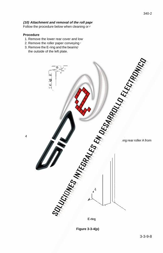
3-3-17
340-2
3-3-9-8
(10) Attachment and removal of the roll paper conveying rear roller AFollow the procedure below when cleaning or replacing roll paper conveying rear roller A.
Procedure1. Remove the lower rear cover and lower left cover.2. Remove the roller paper conveying clutch.3. Remove the E-ring and the bearing retaining the roll paper conveying rear roller A from
the outside of the left plate.
Figure 3-3-4(o)
4. Open the upper right side cover and remove the waste toner tank.5. Remove the E-ring and the bearing retaining the roll paper conveying rear roller A from
the outside of the right side plate.
Figure 3-3-4(p)

3-3-18
340-2
3-3-9-9
6. Remove the roll paper conveying rear roller A from the main unit.• When attaching, make sure that the longer of the two thin ends of the shaft is
positioned on the left as shown in the figure.7. After cleaning or replacement, refit the removed parts to their original positions.
Figure 3-3-4(q)

3-3-19
340-2
This page is intentionally left blank.

340
3-3-10
3-3-3 Main charger section
(1) Replacing the drumReplace the drum as follows.
Caution :After replacing the drum be sure to clean the main charger assembly and check the drumsurface potential (see page 3-3-18) after coating the cleaning blade with toner (simulationNo. 40).
Procedure1. Detach the cleaning assembly.2. Turn the flywheel clockwise to disengage the flywheel joint from the drum flange.
• When pulling the flywheel, align the screw head on the flywheel shaft with the cutoutin the flywheel stopper.
• When refitting the drum, turn the flywheel clockwise until it clicks to engage the drumflange with the flywheel joint.
Flywheel
Screw headCutout
Flywheel shaft
Flywheel stopper
Figure 3-3-5

340
3-3-11
3. Remove the screw on the drum left rail guide.4. While holding the drum release plate toward the drum, slide the drum left rail guide
toward the machine rear. The drum release plate is locked and the drum flange isunlocked from the drive joint.
Drum release plate
Drum left rail guide
Figure 3-3-6
5. Loosen the two screws of the drum right and left stoppers holding both ends of the drumand unlock the stoppers.
Screws
Drum left stopper Drum right stopper
Figure 3-3-7
340-1

340
3-3-12
6. Remove the screw and raise the drum right rail guide.7. Attach the screw removed in step 6 to part A so that the main unit is kept open.8. Roll the drum toward you along the drum right rail guide.9. Detach the drum from the main unit.
Drum right rail guide
Drum
A
Figure 3-3-8
10. After replacement, return the parts to their original positions.• When the drum has been replaced, fit the drum right flange to the end with the label
inside of the drum.
Drum
Drum right flange
Label
Electrode
Figure 3-3-8 (a)
340-1

340
3-3-13
(1-1) Cleaning the drum electrodes
Procedure• Cleaning the electrode on the drum right flange1. Detach the cleaning assembly.2. Remove the screw on the drum left rail guide (see page 3-3-11).3. While pressing the drum release plate toward the drum, slide the drum left rail guide
toward the machine rear. The drum release plate is locked and the drum flange isunlocked from the drive joint (see page 3-3-11).
4. Remove the screw and open the right upper side cover.5. While turning the flywheel, clean the outer periphery of the electrode on the drum right
flange with alcohol.
Electrode FlywheelDrum right flange
Figure 3-3-8 (b)
• Cleaning the electrode on the drum right holder1. Detach the drum from the main unit.2. Clean the drum electrode, the part in contact with the electrode on the drum right flange,
using alcohol.
Drum right holderDrum electrode
Figure 3-3-8 (c)
340-1
3-3-12-1

340
3-3-14
340-1
This page is intentionally left blank.

340
3-3-13
(2) Cleaning the drumFollow the procedure below when image errors occur.
Caution:• Avoid direct sunlight and strong light when cleaning the drum.• Dust in the air and from the cleaning pad may damage the drum during operation. Avoid
working in dusty place.• Clean the drum entirely even if it is only dirty locally.• Do not clean the drum with alcohol, thinner or other organic solvent.
Required supplies• Toner• Polishing cloth: specified synthetic cotton
Procedure1. Detach the drum from the main unit.2. Apply a polishing cloth to the drum and gently wipe the drum taking care not to damage
the surface.3. Apply toner to another cloth and wipe the drum surface with it in the same manner.4. Refit the drum and all the removed parts, and let the copier stand for about 30 minutes.5. Make a test copy and check the image.
Polishing clothDrum
Figure 3-3-9

340
3-3-14
(3) Changing the charger wireFollow the procedure below when the charger wire is broken or when replacing the chargerwire.
Caution:• Use the specified tungsten wire for the charger wire. (Item No. 74716280, Anodized
tungsten wire, 0.08 mm)• The section wound around the charger spring should not protrude from the main charger
housing.• The end of the charger wire should not protrude from under the screw.• Be sure to use tungsten wire that is free of soiling or damage.• Keep the charger wire taut by stretching the charger spring.• When changing the charger wire, be sure to clean the individual sections of the main
charger assembly (inside of charger housing, etc).• Do not use organic solvents such as alcohol and thinner to clean the main charger
shied.
Procedure1. Detach the cleaning assembly.2. Rotate the main charger assembly in the direction shown by the arrow and detach the
main charger assembly from the cleaning assembly.
Main charger assembly
Cleaning assembly
Figure 3-3-10
340-1

340
3-3-15
3. Remove the right and left main charger lids.4. Remove the charger spring from the main charger terminal and loosen the screw to
remove the charger wire.
Main charger terminal
Charger spring
Main charger left lid
Main charger right lid
Washer
Screw
Tungsten wire
Figure 3-3-11
5. Wind the tungsten wire five turns around one end of the charger spring, and trim the endof the wire.• The length of the cut wire must be less than 1 mm.
1 Fold over the end of the tungsten wire.
3 Wind five turns.
2 Pass the folded end through the end of the charger spring.
Figure 3-3-11 (a)
340-1

340
3-3-16
6. Hook the charger spring to the main charger terminal and pass the tungsten wire throughthe opening in the wire adjustment plate.
7. Pass the tungsten wire under the washer and fasten it with the screw keeping thecharger wire stretched so that the charger spring is at least 16 mm long.
8. Cut off the excess wire under the washer so less than 2 mm protrudes.
Screw
Washer
Trim
2 mm or less
Tungsten wire
1 mm or less
Wire adjuster
16 mm or longer
Main charger terminal
Wind (5 mm or less)
Figure 3-3-12
9. Turn the adjustment screw of the wire adjustment plate until 1.0 ± 0.5 mm of its tipprotrudes to adjust the height of the wire adjustment plate.
Wire adjustment plate
Adjustment screw
1.0 ± 0.5 mm
Figure 3-3-13
340-1
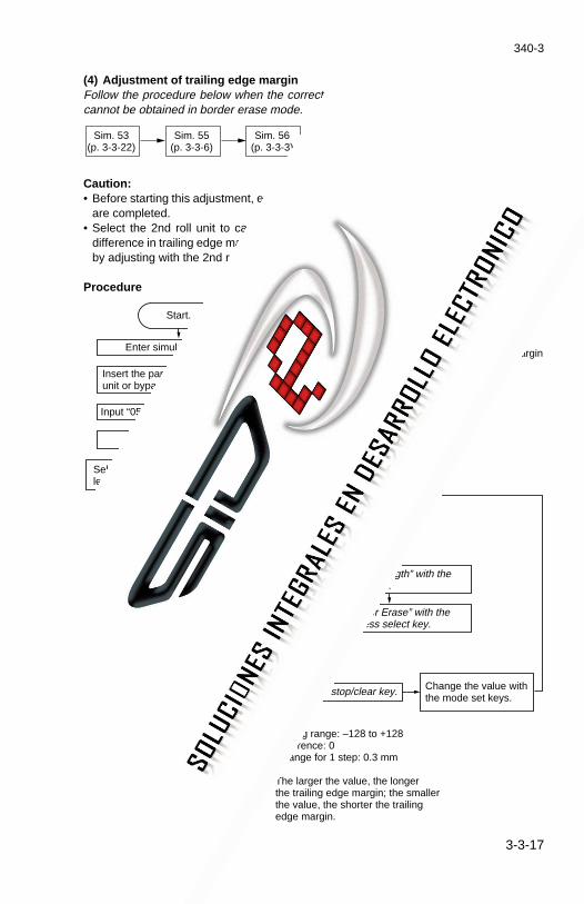
3-3-17
340-3
(4) Adjustment of trailing edge marginFollow the procedure below when the correct trailing edge margin (border erase width)cannot be obtained in border erase mode.
Caution:• Before starting this adjustment, ensure that all the adjustments in the above simulations
are completed.• Select the 2nd roll unit to carry out test copying for roll paper feed adjustment. The
difference in trailing edge margin in normal copy operation for each roll unit is minimizedby adjusting with the 2nd roll unit selected (as standard selection).
Procedure
Start.
End.
Enter simulation mode.
Input “058” with the numeric keys.
No
Yes
Press the enter key.
Select “REAR BLANK ADJ” with the leading edge margin key.
Press the enter key.
Press the stop/clear key.
Insert the original and make a test copy.
Exit simulation mode.
Is the trailing edge margin equal to the initial border erase width
setting?
Change the value with the mode set keys.
Setting range: –128 to +128 Reference: 0 Change for 1 step: 0.3 mm The larger the value, the longer the trailing edge margin; the smaller the value, the shorter the trailing edge margin.
Select the paper feed position in which the paper is inserted (2nd roll unit, bypass table) with the paper source key.
Insert the paper in the 2nd roll unit or bypass table.
Press the stop/clear key.
Select “Paper Length” with the paper length key.
Select “Border Erase” with the image process select key.
Figure 3-3-14
Original Copy example
Trailing edge margin
Sim. 53 (p. 3-3-22)
Sim. 59 (p. 3-3-7)
Sim. 58
Sim. 55 (p. 3-3-6)
Sim. 56 (p. 3-3-3)

3-3-18
340-3
(5) Checking drum surface potentialFollow the procedure below after replacing the drum, LPH and drum potential sensor.
Procedure
Test pattern 1
Approx. 3 cm
Test pattern 2 Test pattern 3
The image is visible from around the 6th tone for test pattern 1, from around the 3rd tone for test pattern 2, and from around the 9th tone for test pattern 3.
63
9Start.
End.
Enter simulation mode.
Input “103” with the numeric keys.
No
Yes
Press the enter key.*
Input “035” with the numeric keys and press the enter key.
Press the stop/clear key.
Exit simulation mode.
Is the copy image correct
(test pattern 1)?
Reference “TRGT” is displayed.
Change the setting with the arrow UP/DOWN mode set keys.
The test pattern is output.
Press the stop/clear key.
*To abort test pattern output, press the job stop/roll cut key.
If Test pattern 2 is printed, decreasethe setting by 2~3 increaments.If Test pattern 3 is printed, increasethe setting by 2~3 increaments.
Press the stop/clear key.
Select "LPH ON" using the LeftMargin + - Keys.
Figure 3-3-15
340-5

3-3-19
340-3
3-3-4 Exposure and original feed section
(1) Attachment and removal of fluorescent lampFollow the procedure below when cleaning or replacing the fluorescent lamp.
Caution :After cleaning or replacing the fluorescent lamp, select copy contrast indicator 4 and makea test copy to check the image in each original mode.If an exposure error occurs in the test copy, adjust the exposure amount (see page 3-3-24).
Procedure1. Open the original holding section.2. Remove the operation section.3. Remove the two screws and remove the left and right center original covers.
Figure 3-3-16
Screw
Left center original cover
Right center original cover
Screw

3-3-20
340-3
4. Remove the four screws and the right and left contact glass retainers.5. Remove the contact glass.6. Remove the hinge left cover and upper left cover.
Figure 3-3-17
Screws
Hinge left cover
Contact glass
Contact glass retainer
Upper left cover
Screws
Contact glass
Contact glass retainer

3-3-21
340-3
7. Remove the two screws securing the fluorescent lamp socket mount at the machineleft.
8. Remove the fluorescent lamp by pulling it out of the fluorescent lamp heater.• When reattaching the fluorescent lamp, be sure to orient it with the manufacturer's
mark on the right side of the copier.9. After cleaning or replacing, return the parts to their original positions.
Manufacturer’s mark
Fluorescent lamp
Fluorescent lamp socket mount Fluorescent lamp
Screws
Figure 3-3-18

3-3-22
340-3
(2) Adjustment of 100% magnificationFollow the procedure below when the magnification is not obtained.
Caution:• Select the 2nd roll unit to carry out test copying for roll paper feed adjustment. The
difference in magnification in normal copy operation for each roll unit is minimized byadjusting with the 2nd roll unit selected (as standard selection).
Procedure
Start.
End.
Enter simulation mode.
Input “053” with the numeric keys.
No
No
Yes
Yes
Press the enter key.
Press the enter key.
Press the stop/clear key.
Insert the original and make a test copy.
Exit simulation mode.
Is the magnification correct in
the main scanning direction?
Select the mode to be adjusted with the leading edge margin key. SIZE ADJ M P: normal paper SIZE ADJ M V: tracing paper (vellum) SIZE ADJ M F: film
Change the value with the mode set keys.
Select the mode to be adjusted with the leading edge margin key. SIZE ADJ S P: normal paper SIZE ADJ S V: tracing paper (vellum) SIZE ADJ S F: film
Setting range: –3.0% to +3.0% Reference: 0 Change for 1 step: 0.1% The larger the value, the longer the copy image; the smaller the value, the shorter the copy image.
Select the 2nd roll unit with the paper source key.
Select the type of paper inserted in the 2nd roll unit with the special paper select key. SIZE ADJ M P: normal paper SIZE ADJ M V: tracing paper (vellum) SIZE ADJ M F: film
Is the magnification correct in
the sub scanning direction?
Insert the paper in the 2nd roll unit.
Figure 3-3-19
Main scanning direction
Sub scanning direction

3-3-23
340-3
(3) Adjustment of leading edge registrationFollow the procedure below when there is a regular error between the leading edges of theoriginal and the copy image.
Caution:• Before starting this adjustment, ensure that all the adjustments in the above simulations
are completed.• Draw a line 10 mm from the leading edge of the document.
Procedure
Figure 3-3-20
Start.
End.
Enter simulation mode.
Input “054” with the numeric keys.
Yes
Yes
No
No
Press the enter key.
Press the enter key.
Press the stop/clear key.
Insert the original and make a test copy.
Exit simulation mode.
Increase the value with the mode set keys.
Decrease the value with the mode set keys.
Setting range: –128 to +128 Reference: 0 Change for 1 step: 4 ms The larger the value, the earlier the original image read-in timing; the smaller the value, the later the original image read-in timing.
Is length A from the line to the
leading edge shorter than 10 mm (copy example 1)?
Is length A from the line to the
leading edge longer than 10 mm (copy example 2)?
Sim. 53 (p. 3-3-22)
Sim. 57 (p. 3-3-5)
Sim. 54
10 mm
Line
Original Copy example 1
Copy example2
A A

1-1-24
340

340-3
(4) Adjustment of exposure amountFollow the procedure below when cleaning or replacing the fluorescent lamp and contactglass, or when an image error occurs on test copies.Also, perform when it is not possible to obtain a good copy image when a correct mode isselected for the original.
• Adjustment for black & white (character) modeRequired originals• When adjusting in the normal original mode: Test chart• When adjusting in the dark original mode: Newspaper test chart (NPTC)• When adjusting in the light original mode: Blue graph paper
Procedure
Enter simulation mode.
Input “140” with the numeric keys.
Yes
Yes
No
No
Start.
End.
Press the enter key.
Select the original mode to be adjusted with the original contrast or auto/manual contrast select key. EXP(PLAIN): normal original mode EXP(DARK): dark original mode EXP(LIGHT): light original mode
Press the enter key.
Press the stop/clear key.
Exit simulation mode.
Insert the original and make a test copy.
Is the image too light? (Copy example 1)
Is the image too dark? (Copy example 2)
Decrease the value with the mode set keys.
Increase the value with the mode set keys.
Setting range: 0 to 8 Reference: 4 The larger the value, the lighter the copy image; the smaller the value, the darker the copy image.
Original Copy example 1
Copy example 2
AA A
A AA
A A
A AA
A A
A A
Figure 3-3-20(a)
3-3-24

340-3
• Adjustment for half tone modeRequired originals• When adjusting in the normal original mode: Test chart• When adjusting in the dark original mode: Dark poster• When adjusting in the light original mode (dark background): Map• When adjusting in the light original mode (light background): Test chart
Procedure
Enter simulation mode.
Input “140” with the numeric keys.
Yes
Yes
No
No
Start.
End.
Press the enter key.
Select the original mode to be adjusted with the original contrast or auto/manual contrast select key. EXP (HALF-PLAIN): normal original mode EXP (HALF-DARK): dark original mode EXP (HALF-LIGHT-BD): light original mode (dark background) EXP (HALF-LIGHT-BL): light original mode (light background)
Press the enter key.
Press the stop/clear key.
Exit the simulation mode.
Insert the original and make a test copy.
Is the image too light? (Copy example 1)
Is the image too dark? (Copy example 2)
Decrease the value with the mode set keys.
Increase the value with the mode set keys.
Setting range: 0 to 8 Reference: EXP (HALF-PLAIN): 4 EXP (HALF-DARK): 4 EXP (HALF-LIGHT-BD): 4 EXP (HALF-LIGHT-BL): 5 The larger the value, the lighter the copy image; the smaller the value, the darker the copy image.
Original Copy example 1
Copy example 2
Figure 3-3-20(b)
3-3-24-1

340-3
This page is intentionally left blank.
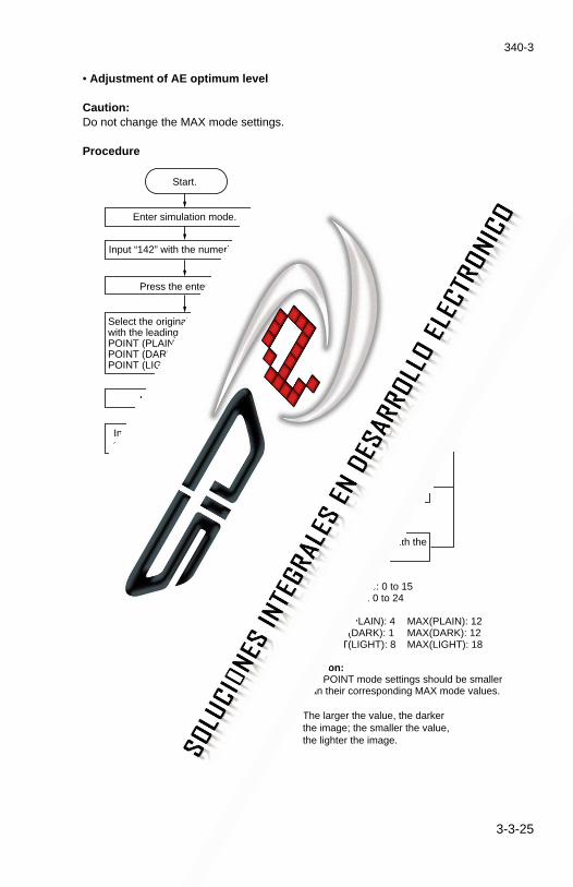
340-3
Enter simulation mode.
Input “142” with the numeric keys.
No
Yes
Start.
End.
Press the enter key.
Press the enter key.
Press the stop/clear key.
Exit simulation mode.
Insert the original and make a test copy.
Is the image too dark?
Decrease the value with the mode set keys. Setting ranges POINT mode: 0 to 15 MAX mode: 0 to 24 References POINT(PLAIN): 4 MAX(PLAIN): 12 POINT(DARK): 1 MAX(DARK): 12 POINT(LIGHT): 8 MAX(LIGHT): 18 Caution: The POINT mode settings should be smaller than their corresponding MAX mode values. The larger the value, the darker the image; the smaller the value, the lighter the image.
Select the original mode to be adjusted with the leading edge margin or left margin key. POINT (PLAIN): normal original mode POINT (DARK): dark original mode POINT (LIGHT): light original mode
No
Is the image too light?
Increase the value with the mode set keys.
Yes
• Adjustment of AE optimum level
Caution:Do not change the MAX mode settings.
Procedure
3-3-25

340-3
3-3-25-1
Examples of required originals and correct images
POINT (PLAIN)
AAAA
AAAA
AAAA
MAX (PLAIN)
AAAA
AAAA
AAAA
MAX (DARK)
AAAA
AAAA
AAAA
MAX (LIGHT)POINT (LIGHT)
POINT (DARK)
• Few black solid areas • Clear high contrast black lines or
characters Example: Plotter prints
• Comparatively many black solid areas • High contrast solid black lines or
characters Example: Posters
• Comparatively many black solid areas • Solid black lines or characters • Visible background Example: Posters with a
photograph/colored background
• Few black solid areas • Clear high contrast black lines or
characters • Visible background Example: Diazo prints
• Characters are not solid black • Visible background Example: Posters with a
photograph/colored background
• Few black solid areas • Lower contrast and less solid black
lines or characters Example: Pencil drawings
POINT
MAX
POINT
MAX
POINT
MAX
Ajustment for normal original mode:
Ajustment for dark original mode:
Ajustment for light original mode:
Figure 3-3-20(c)

340-3
3-3-25-2
• Setting AE fine adjustment intervalsFollow the procedure below when the copy density range is too narrow after the copy densityhas been adjusted with the copy contrast keys in auto contrast mode.
Required original• Test chart
Procedure
Enter simulation mode.
Input “145” with the numeric keys.
Yes
No
No
Start.
End.
Press the enter key.
Press the enter key.
Press the stop/clear key.
Exit simulation mode.
Make test copies at Exp. 4 and Exp. 5 in auto contrast mode and compare the copy density.
Is the copy density range too narrow? (Copy example 1)
Is the copy density range too wide?
(Copy example 2)
Increase the value with the mode set keys.
Yes Decrease the value with the mode set keys.
Setting range: 0 to 8 Reference value: 3 The larger the value, the wider the range of copy density; the smaller the value, the narrower the range of copy density.
EXP.4 Copy example 1 (EXP.5)
Copy example 2 (EXP.5)
Figure 3-3-20(d)
The setting in simulation 142 shifts asthe value in simulation 145 changes.The copy image becomes lighter ordarker based on the LPH output datacorresponding to the scanned imagedata in auto contrast mode.
Scanned image data
LPH
out
put d
ata
0
0 33
0
32
255
Dark
light
Setting value in simulation 145
Setting in simulation 142
88
Figure 3-3-20(e)

340-3
(5) Half tone mode image quality adjustmentFollow the procedure below to adjust the image density to make clear copies of originals withcharacters and photographs or dark posters in half tone mode.
• Adjusting for half tone light original modeRequired original• Original with characters and photographs
Procedure
Enter simulation mode.
Input “141” with the numeric keys.
No
Start.
End.
Press the enter key.
Select “HALF L BL” with the leading edge margin or left margin key.
Press the enter key.
Press the stop/clear key.
Exit simulation mode.
Insert the original and make a test copy.
Is the solid black area too thick?
Decrease the value with the mode set keys.
Setting range: –6 to +14 Reference: 3 The larger the value, the thicker the image; the smaller the value, the thinner the image.
Yes
No
Is the solid black area too thin?
Increase the value with the mode set keys.
Yes
3-3-26
ABCDEFG HIJKLMNO PQRSTUV
ABCDEFG HIJKLMNO PQRSTUV
Correct image Incorrect image
Figure 3-3-20(f)

340-3
• Adjusting for half tone dark original modeRequired original• Dark poster
Procedure
Enter simulation mode.
Input “141” with the numeric keys.
No
Start.
End.
Press the enter key.
Select “HALF D” with the leading edge margin or left margin key.
Press the enter key.
Press the stop/clear key.
Exit simulation mode.
Insert the original and make a test copy.
Is the solid black area too thin?
Increase the value with the mode set keys.
Setting range: –6 to +14 Reference: 0 The larger the value, the thicker the image; the smaller the value, the thinner the image.
YesIs the solid black area too thick?
Decrease the value with the mode set keys.
Yes
No
Correct image
Incorrect image
Figure 3-3-20(g)
3-3-26-1

340-3
This page is intentionally left blank.

340-3
(6) Image contrast adjustment (adjustment of filter gain)Follow the procedure below to make characters clear.
• Adjustment for black & white (character) modeRequired original• Test chart
Procedure
Input “144” with the numeric keys.
No
Yes
End.
Press the enter key.
Select “CHARACTER” with the leading edge margin or left margin key.
Enter simulation mode.
Input “143” with the numeric keys.
Start.
Press the enter key.
Press the stop/clear key.
Select “MODE 2” with the enter key.
Change the value with the mode set keys.
Press the stop/clear key.
Exit simulation mode.
Insert the original and make a test copy.
Is the image contrast correct?
Setting range: 0.1 to 1.9 Reference: 1.0 The larger the value, the stronger the image contrast; the smaller the value, the weaker the image contrast.
Correct image Incorrect image
A AAA AAA AA
A AAA AAA AA
Figure 3-3-20(h)
3-3-27

340-3
• Adjustment for half tone light original mode (dark background)Required original• Map
Procedure
Input “144” with the numeric keys.
No
Yes
End.
Press the enter key.
Select “HALF LIGHT BD” with the leading edge margin or left margin key.
Enter simulation mode.
Start.
Change the value with the mode set keys.
Press the stop/clear key.
Exit simulation mode.
Insert the original and make a test copy.
Is the image contrast correct?
Setting range: 0.1 to 1.9 Reference: 0.5 The larger the value, the stronger the image contrast; the smaller the value, the weaker the image contrast.
Correct image
Incorrect image
Figure 3-3-20(i)
3-3-27-1

340-3
• Adjusting for half tone light original mode (light background)Required original• Test chart
Procedure
Input “144” with the numeric keys.
No
Yes
End.
Press the enter key.
Select “HALF LIGHT BL” with the leading edge margin or left margin key.
Enter simulation mode.
Start.
Change the value with the mode set keys.
Press the stop/clear key.
Exit simulation mode.
Insert the original and make a test copy.
Setting range: 0.1 to 1.9 Reference 0.6 The larger the value, the stronger the contrast; the smaller the value, the weaker the contrast.
Is the tone grada-tion clear?
Correct image
Incorrect image
Figure 3-3-20(j)
3-3-27-2

340
3-3-28
(7) Image focus adjustment (LPH height adjustment)Perform after replacing the LPH.
Procedure1. Enter simulation mode.2. Input “158” with the numeric keys.3. Press the enter key. A test pattern is printed out.
Figure 3-3-21 Test pattern
4. Using a magnifier, check if the lines of the smaller pattern are clearly printed.5. Detach the developing assembly from the main unit.6. Remove the three screws and the LPH lower partition.7. Loosen the six screws holding the LPH.
LPH screws
LPH lower partition
Figure 3-3-22

340
3-3-29
8. Close the LPH lower partition and retighten the three screws.9. Refit the developing assembly to the main unit.
10. Press the enter key and check the test pattern printout.11. Adjust the height of the LPH by turning the adjustment pins on the machine right and
left.• Turn the adjustment pins clockwise (e) to raise the LPH. Turn them counterclockwise
(b) to lower the LPH.
LPH height adjustment pins LPH lower partition
Figure 3-3-23
12. Repeat steps 10 and 11 until the correct test pattern is obtained.13. Press the stop/clear key.14. Exit simulation mode.15. Detach the developing assembly from the main unit.16. Open the LPH lower partition and tighten the six screws for the LPH.
• Fasten one of the two LPH retainers with the lower edges of the pins in contact withthe lower edges of the slots, using the two screws. Fasten the other retainer with theupper edges of the pins in contact with the upper edges of the slots.
17. Close the LPH lower partition and tighten the three screws.18. Refit the developing assembly to the main unit.
Screws
Pins
LPH retainers
Figure 3-3-23 (a)
340-1

340
3-3-30
(8) Replacement of the ISU PCB
Procedure1. Open the main unit.2. Remove the three screws and pull out the ISU mount.3. Remove all the connectors inserted into the ISU PCB.4. Remove the four screws and the ISU PCB.
ISU PCB
ISU mount
Figure 3-3-24
5. Adjust controls VR1, VR3, VR4 and VR5 on the new ISU PCB to their original positionson the old ISU PCB.
ISU PCB
VR3VR1 VR5
VR4
Figure 3-3-25
6. Fit the new ISU PCB to the ISU mount with the four screws.7. Insert the ISU mount and tighten the three screws.8. Close the main unit.9. Execute simulation No. 121 “Adjusting gain” (see page 3-2-30-1).
10. Execute simulation No. 120 “Adjusting γ correction” (see page 3-2-30-1).
340-1

340-1
3-3-30-1
(9) Replacing the LED printhead and LPHROM PCBReplace the LED printhead as follows.
Caution:Always replace the LED printhead and LPHROM PCB as a set. After replacing the LEDprinthead, be sure to adjust the image focus (simulation No. 158: see page 3-3-28).
Procedure1. Remove the lower left cover, lower rear cover, developing assembly, cleaning assembly
and drum.2. Remove the 5P connector of the drum potential sensor and pull it out via the opening
in the left frame.
5P connector
Figure 3-3-25 (a)
3. Remove the three screws and the LPH lower partition.4. Remove the two screws and the two LPH retainers.
Screws
Screw
Screw
Screw
LPH lower partition
LPH retainer LPH retainer
Figure 3-3-25 (b)

340-1
3-3-30-2
5. Remove the two pins.6. Remove the 8P and 60P connectors.7. Take out the LED printhead.
Pin Pin
LED printhead
8P connector 60P connector
Figure 3-3-25 (c)
8. Remove the seven screws and the main PCB cover.9. Remove the two screws, and remove the LPHROM PCB connectors from the main PCB.
Screws
Screws
Main PCB cover
Screws
Main PCB
LPHROM PCB
Figure 3-3-25 (d)

340-1
3-3-30-3
10. Remove the four screws and then the LPH right and left positioning plates & LPHcleaning spring plate.
11. Remove the LPH cleaning lever.
Screws
LPH left positioning plate
LPH right positioning plate
Screw
Screw
LPH cleaning lever
LPH cleaning spring plate
LED printhead
Figure 3-3-25 (e)
12. Refit all the removed parts.

340-1
3-3-30-4
(10) Cleaning the LED printheadPerform the following cleaning when the copy image is faint or a white line appearslongitudinally.
Procedure1. Detach the cleaning assembly, drum and developing assembly.2. Remove the three screws and open the LPH lower partition.3. Slide the LPH cleaning lever back and forth once.
LPH lower partition
Screw
Screw
Screw
LPH cleaning lever
Figure 3-3-25 (f)
4. Refit all the removed parts.

340-1
3-3-30-5
(11) Replacement of the contact image sensorReplace the contact image sensor as follows.
Procedure1. Detach the cleaning assembly and drum.2. Open the upper right side cover (one screw) and detach the lower left cover, operation
unit, left center original cover, right center original cover, hinge left cover, hinge rightcover, upper left cover and upper right cover.
3. Remove the 4P connectors of the fluorescent lamp and fluorescent lamp heater.
Fluorescent lamp heater 4P connector
Fluorescent lamp 4P connector
Figure 3-3-25 (g)
4. Remove the three screws and pull out the ISU mount.5. Remove all the connectors connected to the ISU PCB.
ISU PCB ISU mount
Screw
Screw
Screw
Figure 3-3-25 (h)

340-1
3-3-30-6
6. Remove the two pins and the ISU mount.
Pin
Pin
ISU mount
Figure 3-3-25 (i)
7. Remove the four bundles of contact image sensor wires from the five wire retainers.
Wire retainers
Figure 3-3-25 (j)

340-1
3-3-30-7
8. Remove the seven screws from the original front guide.
Original front guide
Screws
Screws
Screw
Screw
Screw
Figure 3-3-25 (k)
9. Remove the two screws holding the contact image sensor.
Screw Screw
Contact image sensor
Figure 3-3-25 (l)

340-1
3-3-30-8
10. Detach the contact image sensor from the main unit.
Contact image sensor
Figure 3-3-25 (m)
11. Refit all the removed parts.
Caution:Refit the four bundles of contact image sensor wires so that numbers 1 to 4 indicated onthe connectors match the connector numbers CN1 to CN4 on the ISU PCB.
ISU PCB
CN11 2 3 4
CN2 CN3 CN4
Figure 3-3-25 (n)
12. After replacing the contact image sensor, execute simulation No. 121 “Adjusting gain”(see page 3-2-30-1) and then simulation No. 120 “Adjusting γ correction” (see page3-2-30-1).

340-3
3-3-30-9
(12) Adjustment of optical axisFollow the procedure below if there is a regular error between the centers of the original andthe copy image on the paper.
Procedure
Start.
End.
Enter simulation mode.
Input “132” with the numeric keys.
Yes
No
Press the enter key.
Press the enter key.
Press the stop/clear key.
Insert the original and make a test copy.
Exit simulation mode.
Does the center line of the copy
image align with that of original?
Change the value with the mode set keys.• When the test copy looks like copy example 1, increase the value.• When the test copy looks like copy example 2, decrease the value.
Setting range: –3.0 to +3.0 mmChange for 1 step: 0.5 mmReference: 0
The image moves to the left as the value increases, and to the right as the value decreases.
Original Copy example 1 Copy example 2
Figure 3-3-25(o)

340-3
3-3-30-10
(13) Adjustment of the image width in the main scanning directionFollow the procedure below to widen the maximum print width of LPH when the right or leftedge of the copy image is not printed after the optical axis has been adjusted in simulation132.
Caution:• Make a test copy on paper of A1 width (841 mm) using an original of A1 width (841 mm)
or larger with a lateral line drawn from one end to the other.
Procedure
Start.
End.
Enter simulation mode.
Input “133” with the numeric keys.
No
Yes
Press the enter key.
Press the enter key.
Press the stop/clear key.
Insert the original and make a test copy.
Exit simulation mode.
Is right edge or left edge of the copy image missing?
(Copy examples 1 & 2)
Increase the value with the mode set keys.
Setting range: 0.0 to 3.0 mmChange for 1 step: 1.0 mmReference: 0.0 mm
The larger the value, the wider the print width of the image; the smaller the value, the narrower the print width of the image.
Original Copy example 1 Copy example 2
841 mm or larger
Figure 3-3-25(p)

340-3
3-3-30-11
(14) Adjustment for prescan in reduction copy modeFollow the procedure below if a trailing edge margin appears when carrying out synchro cutcopy in reduction copy mode.
Procedure
Start.
End.
Enter simulation mode.
Input “025” with the numeric keys.
No
Yes
Press the enter key.
Press the enter key.
Press the stop/clear key.
Set the magnification to 99%.
Insert the original (A1 lateral) and make a test copy.
Select synchro cut copy mode.
Exit simulation mode.
Is the trailing edge margin 0 mm?
Change the value with the mode set keys.
Setting range: –20 to +20Reference: 0Change for one step: 0.99 mm
(the value differs depending on the magnification set)
The larger the value, the longer the trailing edge margin; the smaller the value, the shorter the trailing edge margin.
Original Copy example
Trailing edge margin
Figure 3-3-25(q)
340-3
3-3-30-12
(15) Setting the shading modeFollow the procedure below to set the exposure lamp light intensity for shading if soil on thecontact glass causes longitudinal lines on the copy image.
Required original• Test chart
Procedure
Enter simulation mode.
Input “113” with the numeric keys.
Yes
Yes
No
Start.
End.
Press the enter key.
Press the enter key.
Press the stop/clear key.
Exit simulation mode.
Insert the original and make a test copy.
Are there any longitudinal lines on the image?
(Copy example 1)Decrease the value with the mode set keys.
No
Is the entire image light? (Copy example 2)
Increase the value with the mode set keys.
Setting range: 30 to 99 (the lamp light intensity for shading)
Reference: 55
The larger the value, the darker the image; the smaller the value, the lighter the image.If the value is too small, a shading problem is detected and copying is disabled even if the original is inserted.
*The lamp light intensity for shading is set to 55 (reference value) when “1: SHADING MODE1” is selected.
Select “2: SHADING MODE2” with the leading edge margin key or left margin key.*
Original Copy example 1 Copy example 2
Figure 3-3-25(r)
340-3
3-3-30-13
(16) Adjustment of leading edge registration (when connected to the interfacecontroller)
Follow the procedure below when the leading edge of the image scanned in scanner modedoes not align with that of the image output in printer mode.
Caution:• Before starting this adjustment, ensure that all the adjustments in the above simulations
are completed.• Draw a line 10 mm from the leading edge of the document.
Procedure
Sim. 53(p. 3-3-22)
Sim. 57(p. 3-3-5)
Sim. 117
Yes
No
No
Start.
Yes
Enter simulation mode.
Input “117” with the numeric keys.
Press the enter key.
Press the enter key.
Press the stop/clear key.
Press the stop/clear key.
Exit simulation mode.
End.
Is length A fromthe line to the leading
edge shorter than 10 mm(copy example 1)?
Is length A fromthe line to the leading
edge longer than 10 mm(copy example 2)?
Scan the original in scanner mode.
Output the scanned image in printer mode.
Increase the value with the mode set keys.
Decrease the value with the mode set keys.
Setting range: –128 to +128Reference: 0Change for 1 step: 4 mm
The larger the value, the earlier the original image read-in timing; the smaller the value, the later the original image read-in timing.
Figure 3-3-25(s)
10 mm
Line
A A
Original Copyexample 1
Copyexample 2
340-4

340-3
3-3-30-14
This page is intentionally left blank.
340-4

340-3
3-3-30-14
This page is intentionally left blank.

340
3-3-31
3-3-5 Developing section
(1) Changing developerFollow the procedure below when replacing the developer.
Procedure1. Remove the lower rear cover.2. Put the plastic bag in the developer collection box.
Plastic bag
Developer collection box
Figure 3-3-26
3. Open the upper right side cover.4. Remove the screw and remove the developing shutter.
Developing shutter
Figure 3-3-27

340-3
3-3-32
5. Close the upper right side cover.6. Remove the 3P connector of the toner feed motor.7. Enter simulation mode.8. Perform simulation “41” (forced stabilization).9. Perform simulation “10” (drive motor operational check).
• The main unit starts operation and the developer is ejected from the developingassembly into the plastic bag in the developer collection box.
10. If no more developer is ejected into the plastic bag after 12 to 15 minutes have elapsed,press the stop/clear key.• The main unit stops operating.
11. Attach the developing shutter to the developing assembly.12. Detach the upper rear cover.13. Remove the developing assembly from the main unit.14. Detach the toner hopper assembly from the developing assembly.15. Remove the developer remaining on the developing roller.16. Attach the developing assembly to the main unit.
• Make sure that the developing assembly is attached at very left-end position so thegears of the developing assembly mesh with the gears of the main unit.
17. Set safety switch 6 to the forced ON position.18. Shake the developer bottle well to mix the developer.19. Perform simulation “10” (drive motor operational check) and pour the developer evenly
into the developing assembly.20. Press the stop/clear key.21. Attach the toner hopper assembly to the developing assembly.
• The 3P connector of the toner feed motor must not be connected.22. Attach the upper rear cover.23. Perform simulation “60” (developer setting).
• After about 3 minutes, the toner control voltage is set automatically and the setting isdisplayed. Be sure to write the displayed value on the simulation label.
24. Turn the main switch off and back on to reset forced stabilization. The copier exits thesimulation mode.
25. Connect the 3P connector of the toner feed motor.26. Remove the plastic bag inserted in the developer collection box.27. Attach the lower rear cover.

340
3-3-33
(2) Adjustment of doctor blade: referencePerform when carrier or dark background appears on copies, or when attaching or removingthe doctor blade.
Procedure1. Remove the developer from the developing assembly. (Follow steps 1 to 14 of changing
developer on page 3-3-31.)2. Detach the screw and the developing unit cover.
Pin
Developing unit cover
Clamp
Screw
Figure 3-3-28
3. Loosen the four screws (two each on the right and left sides) on the doctor blade.
Screws
Figure 3-3-29

340
3-3-34
4. Loosen the six doctor blade adjustment screws on the upper developing unit stay.
Figure 3-3-30
5. Insert a thickness gauge into the five points indicated in the diagram and adjust the gapbetween the doctor blade and the developing roller to the individually specifieddistances by turning adjustment screws 1 and 2.
20 mm 20 mm
1 2 3 4 5
Developing roller
Doctor bladeDoctor blade
Upper developing unit stay
Distances between the doctor blade and the developing roller: 1 5: A 0.7 mm thickness gauge should enter smoothly and a 0.75 mm one should not. 2 4: A 0.65 mm thickness gauge should enter smoothly and a 0.7 mm one should not. 3: A 0.6 mm thickness gauge should enter smoothly and a 0.65 mm one should not.
Screw 1Screw 2
To increase the gap, loosen screw 2 and tighten screw 1. To decrease the gap, loosen screw 1 and tighten screw 2.
Figure 3-3-31
6. Insert developer in the developing assembly and carry out initial setting of the developer(follow steps 15 to 26 of changing developer on page 3-3-32).
7. Make a test copy to check the copy image.
Doctor blade adjustment screws
340
3-3-35
(3) Adjustment of position for magnetic brush: referenceCheck or adjust when the image is faint.
Caution:Before adjusting, check that the position of the doctor blade is correct and that there is theright amount of developer.
Procedure1. Detach the toner hopper assembly from the developing assembly.2. Loosen the two hex screws on the developing roller shaft and adjust the developer roller
bearing so that the distance from the peak of the magnetic brush to the valley of thedeveloping unit housing is 45.2 mm (reference value).• If the position of the magnetic brush is smaller than the specified measurement, carrier
can stick to copies. If the position is larger, dark background can appear on copies.
A
A
Developing roller bearing
A: 45.2 mm
Figure 3-3-32
3. After finishing adjustments, reattach the parts and make a test copy to check the image.

340
3-3-36
(4) Replacement of the lower developing sealReplace the lower developing seal as follows.
Procedure1. Peel the lower developing seal off the developing assembly.2. Attach the new lower developing seal to the developing assembly using double-sided
tape.• Ensure the ends of the seal are aligned with the inner edges A and B of the right and
left developing unit frames so the seal does not crease.
Left developing unit frame
Right developing unit frame
Lower developing seal
Double-sided tapeA
B
Figure 3-3-33

340
3-3-37
3-3-6 Transfer/separation section
(1) Replacement of charger wireFollow the procedure below when the charger wire is broken or when replacing the wire.
Caution:• Use the specified tungsten wire for the charger wire. (Item No. 74716280, Anodized
tungsten wire, 0.08 mm)• The section wound around the charger spring should not protrude from the left transfer
charger housing.• The end of the charger wire should not protrude from under the washer.• Be sure to use tungsten wire that is free of soiling or damage.• Keep the charger wire taut by stretching the charger spring.• When replacing the charger wire be sure to clean the individual sections of the transfer
charger assembly (inside of charger housing, etc).
Procedure1. Open the main unit.2. Remove the screw and then the transfer charger assembly from the main unit by pulling
up in the direction shown by the arrow.
Transfer charger assemblyScrew
Figure 3-3-34
340-1

340
3-3-38
3. Remove the transfer inner shield from the transfer outer shield.
Transfer outer shield
Transfer inner shield
Figure 3-3-35
4. Remove the right and left transfer charger lids and the left and right transfer seals.5. Remove the charger spring from the pin inside the transfer charger left housing and
loosen the screw to remove the charger wire.
Left transfer charger lid
Left transfer seal
Charger spring
Tungsten wire
Right transfer charger lid
Right transfer seal
Screw
Washer
Figure 3-3-36

340
3-3-39
6. Wind the tungsten wire 4-5 times around one end of the charger spring and hang thecharger spring on the protrusion inside the transfer charger left housing.
7. Pass the tungsten wire under the washer and tighten with the screw keeping the chargerwire stretched so that the charger spring is at least 16 mm long.
Figure 3-3-37
8. After wiring, return the parts to their original positions.
Tungsten wire
Greater than 16 mmCharger spring
Twist wire
Cut here
Screw Tungsten wire

340
3-3-40
(2) Replacement of transfer wireFollow the procedure below when the transfer wire is broken or when replacing the wire.
Caution:• Approximately 3.0 m of wire is required to replace the transfer wire.• Use the specified wire (Item No. 74716290).
Procedure1. Loosen the two screws on the bottom of the transfer outer shield and remove the transfer
wire.2. Remove the insulating tube from the transfer wire.
Insulating tube
Figure 3-3-38
3. Wind one end of the transfer wire once around the screw on the right side of the bottomof the transfer outer shield and tighten the screw.• The transfer wire should be passed under the washer. The end should not protrude
more than 5 mm from the washer.
Washer
Screw
5 mm
Figure 3-3-39
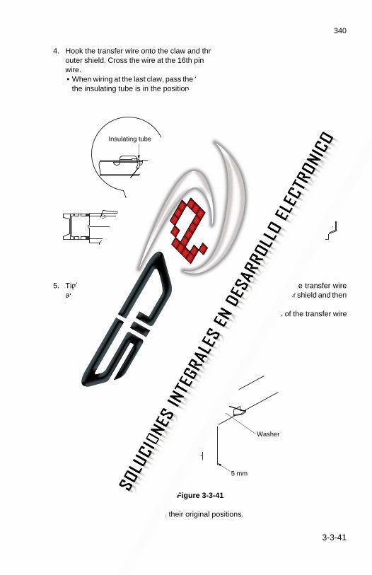
340
3-3-41
4. Hook the transfer wire onto the claw and thread it through the grooves of the transferouter shield. Cross the wire at the 16th pin as shown below and continue to thread thewire.• When wiring at the last claw, pass the transfer wire through the insulating tube so that
the insulating tube is in the position shown in the figure.
1216
Insulating tube
Cross the wire
Figure 3-3-40
5. Tighten the transfer wire to remove any slack and wind one end of the transfer wirearound the screw once on the left side of the bottom of the transfer outer shield and thentighten the screw.• The transfer wire should be passed under the washer. The end of the transfer wire
should not protrude more than 5 mm from the washer.
Screw
Washer
5 mm
Be sure to wind in the direction of the arrow
Figure 3-3-41
6. After wiring, return the parts to their original positions.

340
3-3-42
3-3-7 Cleaning section
(1) Attachment and removal of the cleaning bladeFollow the procedure below when replacing the cleaning blade.
Caution:Coat the cleaning blade with toner (simulation No. 40) after replacing it.
Procedure1. Remove the main charger assembly from the cleaning assembly.2. Loosen the screw and remove the cleaning unit weight.
Cleaning unit weight
Figure 3-3-42
3. Remove the five screws (2 each on right and left, 1 in the center) and the grid assembly.
Screws
Grid assembly
Figure 3-3-43

340
3-3-43
4. Remove the stop rings on the left and right side and remove the bearings.5. Remove the screw on the cleaning seal left and right attachment plates.
Figure 3-3-44
6. Release the cleaning seal left and right attachment plates in the direction shown by thearrow.
7. Remove the cleaning blade.8. Remove the cleaning seal left and right attachment plates from the cleaning blade.
Cleaning blade
Cleaning seal attachment plate
Figure 3-3-45
Stop ring
Bearing
Cleaning seal right attach- ment plate
Cleaning blade
Cleaning blade
Cleaning seal left attachment plate
Bearing
Stop ring
340-1

340
3-3-44
9. Remove the weight mount (two screws) from the cleaning blade and fit it to the newblade.
Cleaning bladeWeight mount
Figure 3-3-46
10. After replacement, return the parts to their original positions.Caution:When refitting the cleaning seal right and left attachment plates, ensure the right and leftcleaning seals (red) are not overriding the seal parts of the lower cleaning blade.
Lower cleaning blade
The lower cleaning blade should be above the cleaning seal.
Left cleaning seal
Cleaning seal left attachment plate
Figure 3-3-47

340
3-3-45
(2) Attachment and removal of lower cleaning bladeFollow the procedure below when replacing the lower cleaning blade.
Procedure1. Loosen the four screws (1 each on right and left, 2 in the center) and remove the lower
cleaning blade.
Lower cleaning blade
Figure 3-3-48
2. After replacement, return the parts to their original positions.• Ensure that the lower cleaning blade is installed all the way toward the machine left.
340-1

340
3-3-46
(3) Attachment and removal of cleaning fur brushFollow the procedure below when cleaning or replacing the cleaning fur brush.
Procedure1. Remove the cleaning blade.2. Remove the stop ring and then remove fur brush gear 17, the shim, pin and the bearing.
PinBearing
Shim
Stop ring
Fur brush gear 17
Figure 3-3-49
3. Remove the stop ring and the bearing.4. Remove the cleaning fur brush.
Cleaning fur brush
Bearing
Stop ring
Figure 3-3-50
5. After cleaning or replacement, return the parts to their original positions.
340-1

340
3-3-47
(4) Attachment and removal of separation clawFollow the procedure below when replacing the separation claw.
Procedure1. Remove the screws on the separation spring.
Separation spring Separation shaft
Figure 3-3-51
2. Remove the separation claw guide.3. Move the separation claw to the D-cut section of the separation shaft and remove the
separation claw from the separation shaft.
Figure 3-3-52
4. After replacement, return the parts to their original positions.• Check that the separation claws move smoothly.
Separation claw guide
Separation claw
D-cut section

340
3-3-48
3-3-8 Fixing section
(1) Attachment and removal of fixing heaters M and SFollow the procedure below when inspecting or replacing fixing heaters M and/or S.
Procedure1. Detach the upper right removal cover, upper left removal cover, lower right removal
cover, and lower left removal cover.2. Disconnect the 1P connectors from both ends of the fixing heaters.3. Remove a screw on each side and remove the left and right heater support plates.4. Remove the fixing heaters by pulling them out of the heat roller.
• When reattaching the fixing heaters, be sure that the blue 1P connector (for fixingheater S) is on the front of the copier and the white one (for fixing heater M) is on therear.
Figure 3-3-53
5. After inspecting or replacing, return the parts to their original positions.
Left heater support plate1P connectors
Fixing heater S
Fixing heater M
B W
Fixing heater S
Fixing heater M
White 1P connector
Blue 1P connector
Right heater support plate
340-1

340
3-3-49
(2) Attachment and removal of heat rollerFollow the procedure below when cleaning or replacing the heat roller.
Procedure1. Remove fixing heaters M and S (see page 3-3-48).2. Press the fixing section release lever to open the fixing section.3. While holding up the fixing section, remove the left and right fixing release sliders from
the upper release pivot pin.4. Open the fixing section all the way.
Upper release pivot pin
Fixing release slider
Figure 3-3-54
5. Fasten the right fixing unit frame with the screw to keep the fixing unit open.
Right fixing unit frame
Screw
Figure 3-3-55

340
3-3-50
6. Remove the middle removal cover.7. Remove the 2P connector of the eject switch, the 3P connector of the fixing unit pulse
sensor, the two screws and the upper eject guide.
Upper eject guide
3P connector
2P connector
Figure 3-3-56
8. Remove the C-ring, the heat roller gear, the bearing retainer (two screws), and the heatroller bearing on the heat roller left side.
Heat roller
Bearing retainerC-ring
Heat roller gear
Heat roller bearing
Screws
Figure 3-3-57
340-1

340-3
3-3-51
9. Remove the C-ring, the bearing retainer (two screws) and the heat roller bearing on theheat roller right side.
10. Remove the heat roller.
Heat roller
Heat roller bearing
Bearing retainer
C-ring
Figure 3-3-58
11. After cleaning or replacement, return the parts to their original positions.
Important: After replacement of the heat roller, the separation claws may leave lines onsolid black copies if sufficient silicon oil is not applied on the roller surface. Topreempt this problem, perform simulation 10 for 10 minutes or more after heatroller replacement.

340-3
3-3-52
(3) Attachment and removal of the press rollerFollow the procedure below when cleaning or replacing the press roller.
Procedure1. Remove the left and right fixing unit release sliders from the upper release pivot pin and
open the fixing section all the way (see page 3-3-49).2. Fasten the right fixing unit frame with the screw to keep the fixing unit open (see page
3-3-49).3. Remove the screw and pin, and remove the lower eject guide.
Screw
Pin
Lower eject guide
Figure 3-3-59
4. Release the fixing unit front guide by lifting it up in the direction shown by the arrow.5. Remove the press roller from the main unit.6. Remove the press roller shaft from the press roller by pulling it out.
Fixing unit front guide
Press roller
Press roller shaft
Press roller
Figure 3-3-60
7. After cleaning or replacement, return the parts to their original positions.• Apply a small amount of silicon oil (Item No. 49925515-silicon oil SH200) to the
surface of the temperature detection sections of fixing unit thermistors 3 and 4.8. Make test copies until the silicon oil applied to fixing unit thermistors 3 and 4 no longer
shows.
Important: After replacement of the press roller, the separation claws may leave lines onsolid black copies if sufficient silicon oil is not applied on the roller surface. Topreempt this problem, perform simulation 10 for 10 minutes or more after pressroller replacement.

340
3-3-53
(4) Attachment and removal of oil rollerFollow the procedure below when replacing the oil roller.
Procedure1. Detach the upper right removal cover, upper left removal cover, lower right removal
cover, and lower left removal cover.2. Remove the four screws and the 4P and 5P connectors and then detach the original
table assembly.
4P connector
Original table assembly
5P connector
Figure 3-3-61
3. Remove the two screws and detach the fixing unit cover.
Fixing unit cover
Figure 3-3-62

340
3-3-54
4. Remove the crimp springs on the right and left of the oil roller.
Crimp spring
Figure 3-3-63
5. Loosen the hex-socket-head screw and remove gear 27T from the left of the oil roller.6. Remove the E-rings on the left and right of the oil roller and remove the bearings.
E-rings
Bearing
Hex-socket-head screw
Gear 27T
Bearing
Figure 3-3-64

340
3-3-55
7. Remove the oil roller.
Oil roller
Figure 3-3-65
8. After replacement, return the parts to their original positions.

340
3-3-56
(5) Attachment and removal of fixing unit thermistors 1 and 2Follow the procedure below when inspecting or replacing fixing unit thermistors 1 or 2.
Procedure1. Remove the upper right removal cover, upper left removal cover, lower right removal
cover, and lower left removal cover.2. Remove the original table assembly and the fixing unit cover (see page 3-3-53).3. Remove the screw and the 2P connector (right side of main unit). Remove fixing unit
thermistor 1 or 2.• When reattaching fixing unit thermistor 1 or 2, be sure that the surface of the thermistor
is in contact with the heat roller. Insert the black 2P connector of fixing unit thermistor1 into the black 2P plug of the thermistor relay wire, and the white 2P connector of fixingunit thermistor 2 into the white 2P plug.
Fixing unit thermistor 2
White 2P connector
Black 2P connector
Fixing unit thermistor 1
Figure 3-3-66
4. After inspection or replacement, return the parts to their original positions.

340
3-3-57
(6) Attachment and removal of fixing unit thermal switches 1 and 2Follow the procedure below when inspecting or replacing fixing unit thermal switches 1 or2.
Caution:• When replacing the fixing unit thermal switches (thermostats), be sure to use the specified
parts.• If wires are used instead of the specified fixing unit thermal switches (thermostats), the
copier may be seriously damaged.
Procedure1. Remove the upper right removal cover, upper left removal cover, lower right removal
cover, and lower left removal cover.2. Remove the original table assembly and the fixing unit cover (see page 3-3-53).3. Remove the two screws and 1P connector of each fixing thermal switch and then the
thermal switch relay wire. Detach fixing thermal switch 1 or 2.
Thermal switch relay wire
1P connector
1P connector
Fixing unit thermal switch 1
Fixing unit thermal switch 2
Figure 3-3-67
4. After inspection or replacement, return the parts to their original positions.

340
3-3-58
(7) Attachment and removal of fixing unit thermistors 3 and 4Follow the procedure below when inspecting or replacing fixing unit thermistors 3 or 4.
Procedure1. Remove the left and right fixing unit release sliders from the upper release pivot pin and
open the fixing section all the way (see page 3-3-49).2. Fasten the right fixing unit frame with the screw to keep the fixing unit open (see page
3-3-49).3. Remove the two screws and remove the lower eject guide. (see page 3-3-52).4. Remove the screw, the 2P connector and fixing unit thermistor 3 or 4.
• When reattaching fixing unit thermistor 3 or 4, be sure that the surface of the thermistoris in contact with the press roller while closing the fixing section.
Fixing unit thermistor 4
Fixing unit thermistor 3
Figure 3-3-68
5. After inspection or replacement, return the parts to their original positions.

340
3-3-59
(8) Attachment and removal of the external temperature thermistorFollow the procedure below when inspecting or replacing the external temperaturethermistor.
Procedure1. Remove the lower left cover.2. Remove the screw and the 2P connector and remove the external temperature
thermistor.
External temperature thermistor
2P connector
Figure 3-3-69
3. After inspection or replacement, return the parts to their original positions.

340
3-3-60
3-3-9 Other sections
(1) Adjusting the tension of paper feed section drive belt 1Follow the procedure below when attaching or removing the paper feed motor or whenreplacing paper feed section drive belt 1.
Procedure1. Remove the lower left cover.2. Loosen the screw on paper feed drive tension plate 1.3. Tighten the screw so that the edge of the protrusion on paper feed drive tension plate
1 and the center of the screw align.
Paper feed section drive belt 1
Screw
Protrusion
Paper feed drive tension plate 1
Figure 3-3-70
4. After adjustment, return the parts to their original positions.

340
3-3-61
(2) Adjusting the tension of paper feed section drive belt 2 [when installing 3rdroll unit (optional) only.]
Follow the procedure below when replacing paper feed section drive belt 2.
Procedure1. Remove the lower left cover.2. Loosen the screw on paper feed drive tension plate 2.3. Tighten the screw so that the end of paper feed drive tension plate 2 is in the center of
the hole of roll drive assembly B.
Paper feed section drive belt 2
Edge
Paper feed drive tension plate 2
Roll drive assembly B
Hole
Figure 3-3-71
4. After adjustment, return the parts to their original positions.

340
3-3-62
(3) Adjusting the tension of the cutter drive beltFollow the procedure below when attaching or removing the cutter unit or when replacingthe cutter drive belt.
Procedure1. Remove the lower left cover.2. Loosen the screw on the cutter drive tension plate.3. Tighten the screw so that the screw is in the center of the long hole of the cutter drive
tension plate.
Cutter drive tension plate
Cutter drive belt
Screw
Figure 3-3-72
4. After adjustment, return the parts to their original positions.

340-3
3-3-63
(4) Adjusting the tension of original feed drive belt 1Follow the procedure below when attaching or removing the original feed clutch or whenreplacing original feed drive belt 1.
Procedure1. Open the upper right side cover.2. Loosen the two screws on the original drive tension plate.3. Tighten the two screws while the original drive tension plate is pulled by the tension
spring.Note: Do not stretch the tension spring excessively.
Origianl feed drive belt 1
Screws
Original drive tension plate
Tension spring
Figure 3-3-73
4. After adjustment, return the parts to their original positions.

340
3-3-64
(4-1) Adjusting the tension of the developing drive beltFollow the procedure below when replacing the developing drive belt.
Procedure1. Remove the lower left cover.2. Loosen the screw holding the developing drive tension plate.3. Retighten the screw with the edge of the developing drive tension plate aligned with the
center of the hole in the developing drive mount.
Hole
Developing drive mount
Developing drive belt
Screw
Developing drive tension plate
Figure 3-3-73 (a)
340-1
3-3-63-1

340
3-3-65
340-1
This page is intentionally left blank.

340
3-3-66
(5) Attachment and removal of ozone filterFollow the procedure below when replacing the ozone filter.
Procedure1. Open the main unit.2. Remove the lower left cover.3. Remove the screw and then the ozone filter retainer.4. Remove the screw and the ozone filter.
Ozone filter
Ozone filter retainer
Figure 3-3-74
5. After replacement, return the parts to their original positions.
3-3-64

1-1-25
340
CONTENTS
3-4 PCB Initial Settings
3-4-1 Main PCB ............................................................................................ 3-4-13-4-2 Non-field-adjustable volume controls .................................................. 3-4-3

340
3-4-1
3-4-1 Main PCB
When replacing the main PCB, simply fit the backup PCB that was attached to the old mainPCB to the new main PCB. However, if the backup PCB is going to be replaced, it isnecessary to take the following procedure.
Procedure• With the backup PCB that has been used 1. Record the following data of user-set items.
• Settings used in program copy mode• Initial copy settings
2. Enter the simulation mode. 3. Run the following simulations and record the counts.
4. Exit the simulation mode. 5. Turn the main switch off and disconnect the power plug. 6. Replace the backup PCB.
Sim. No. Counts to be recorded
72 Maintenance count73 Total counter count74 Jam counts by the paper source76 Total counts by the paper source

340-3
3-4-2
Sim. No. Contents
25 Adjustment for prescan in reduction copy mode26 Setting delay before original feed start31 Ignoring developing control35 Entering drum surface potential data for black & white mode36 Entering drum surface potential data for half-tone mode46 Setting fixing stabilization at low speed53 Adjusting 100% magnification54 Adjusting leading edge registration55 Adjusting synchrocut length (297 mm)56 Adjusting synchrocut length (1189 mm)57 Adjusting the leading edge margin58 Adjusting trailing edge margin/displayed synchrocut length59 Adjusting the paper cut position for specified length cut mode63 Checking/changing toner control voltage66 Entering toner sensor control level/copy count67 Selecting operation under the empty toner condition71 Selecting the maintenance cycle (metric models only)75 Entering the service telephone No.80 Switching the counter counting units81 Selecting the language82 Selecting between key counter/card84 Selecting the No. of exposure steps86 Switching the fixing temperature87 Disabling cancellation of auto shutoff function89 Setting optional roll unit92 Setting potential correction intervals94 Setting the maximum copy length for multiple copy mode95 Setting the maximum copy length for roll/bypass mode96 Selecting the action after paper empty detection97 Switching between front and rear ejection of originals98 Selecting the copy count timing
109 Setting the controller type113 Setting the shading mode115 Selecting the connection to the interface controller116 Setting the time to return from the offline condition117 Adjusting the leading edge registration (when connected to the interface
controller)132 Adjusting optical axis
• With the new backup PCB 7. Connect the power plug and turn the copier main switch on. 8. Enter the simulation mode. 9. Run simulations 70 and 85.10. Clean the contact glass and middle upper original roller.11. Run simulation 120 to conduct γ correction.12. Run simulation 83 to select between inch and metric specifications.13. Run the following simulations and enter the data recorded on the simulation label.

340-3
3-4-3
14. Exit the simulation mode.15. Enter the data of user-set functions recorded in step 1.
3-4-2 Non-field-adjustable volume controls
Some of the volume controls that have been adjusted at the factory before shipment cannotbe readjusted in the field. Handle these controls carefully.Keep hands away from the non-field-adjustable controls shown below:• Main high-voltage transformer: VRG, VRMC• ST high-voltage transformer: VR1, VR11, VR21• Developing bias high-voltage transformer: VR1• Drum potential sensor PCB: VR1, VR3• Power source PCB: RV1, RV2• LPH power source PCB: RV1
133 Adjusting the image width in the main scanning direction140 Adjusting exposure amount141 Adjusting half-tone image quality (dark/light)142 Adjusting AE optimum level143 Switching filter modes144 Adjusting filter gain145 Setting AE fine adjustment intervals153 Selecting current correction value160 Adjusting base 4 output density161 Adjusting thresholds (central exposure level)163 Adjusting Exp. 1.0 threshold164 Adjusting Exp. 7.0 threshold165 Setting the memory unit connection166 Selecting display of the “Output?” screen after restart167 Setting the AE scan168 Setting the maximum number of continuous copies178 Selecting memory output mode
Sim. No. Contents

1-1-26
340

1-1-27
340
CONTENTS
3-5 Self Diagnostics
3-5-1 Self-diagnostic function ....................................................................... 3-5-1(1) Self-diagnostic display ................................................................. 3-5-1

340
3-5-1
3-5-1 Self-diagnostic function
(1) Self-diagnostic displayThis unit is equipped with a self-diagnostic function. When it detects a problem with itself,it disables copying and displays a self-diagnostic code (C-xxx) indicating the nature of theproblem together with the message requesting to call for service on the display.After removing the problem, the self-diagnostic function can be reset by opening and closingthe main unit (SSW4 and 5 turning off and on) or turning the main switch off and back on.
Metric
Inch
Figure 3-5-1 Service call code display
Call for service TEL
C-XXX
CALL FOR SERVICE TEL
C-XXX

340-3
3-5-2
C-10
C-11
C-31
Self diagnostic codes
Code ContentsRemarks
Causes Check procedures/corrective measures
Backup RAM problemCollapse in data pattern ofthe specified area of theRAM has been found dur-ing 20-s-interval detectionright after power on.
Wrong main ROM ver-sionIt has been found rightafter power on that ver-sions of the two ROMs(IC83 and IC93) on themain PCB are differentfrom each other.
Communication problemon servo PCBResponse to the mainPCB from servo motorcontrol 2 PCB has notbeen made within 160 msafter communication start.
A checksum error hasoccurred.
The SRAM(IC1, IC3) onthe backupPCB has aproblem.
The backupPCB or mainPCB is defec-tive.
Two ROMsthat havedifferent ver-sions to eachother are in-stalled.
Servo motorcontrol 2 PCBis defective.
The mainPCB is defec-tive.
Run simulation 70 and resetthe memory contents.
If C-10 persists after reset-ting the memory contents,replace the backup PCB ormain PCB.
Check the versions and in-stall ROMs of the same ver-sion.
Replace servo motor control2 PCB and check operation.
Replace the main PCB andcheck operation.

340-3
3-5-3
Check the connection ofCON3 on the interface PCBand continuity across theconnector terminals. If thereis any abnormality, remedyor replace.
Check the connection andcontinuity of the interfacecable. If there is any abnor-mality, replace the cable.
Replace the PROM (IC54)on the interface PCB andcheck operation.
Check the connection ofCN20 on the copier mainPCB and continuity acrossthe connector terminals. Ifthere is any abnormality,remedy or replace.
Replace the copier mainPCB and check operation.
Code ContentsRemarks
Causes Check procedures/corrective measures
C-33 Interface controller com-munication problemCommunication betweenthe copier and interfacecontroller is interrupted for2 s or more in printermode or scanner mode.
Poor contactin the connec-tor terminalsof CON3 onthe interfacePCB.
The interfacecable is de-fective.
The PROM(IC54) on theinterface PCBis defective.
Poor contactin the connec-tor terminalsof CN20 onthe copiermain PCB.
The copiermain PCB isdefective.
C-34 Communication problemwith the ISUResponse to the mainPCB from the ISU PCBhas not been made within64 ms during operation.
Six checksum errors haveoccurred in succession.
The ISU PCBis defective.
The mainPCB is defec-tive.
Replace the ISU PCB andcheck operation.
Replace the main PCB andcheck operation.
3-5-2-1

340-3
3-5-4
This page is intentionally left blank.

340-1
3-5-5
Code ContentsRemarks
Causes Check procedures/corrective measures
C-36
C-37
C-300
C-301
C-510
IPC1 problemProcessing request givento communication CPUIC22 fails to be processedwithin 512 ms.
IPC2 problemProcessing request givento communication CPUIC110 fails to be proc-essed within 512 ms.
ISU sequence problemNecessary response failsto be emitted from ISUPCB within 2 s after a re-quest.
Jam indication J-05 is dis-played each time an origi-nal is inserted, six times insuccession.
Servo PCB hardwareerrorAn error signal has beenemitted from servo motorcontrol 2 PCB.
Main charger leakageShorting alarm signal (MCALARM) is detected forfive times in succession at200-ms intervals whilemain charger output isbeing generated.
The mainPCB is defec-tive.
The mainPCB is defec-tive.
The fluores-cent lamp hasa break.
The fluores-cent lampconnectorterminalsmake poorcontact.
The ISU PCBis defective.
Servo motorcontrol 2 PCBis defective.
The maincharger leaks.
The maincharger wireis broken.
The mainhigh-voltagetransformer isdefective.
Replace the main PCB andcheck operation.
Replace the main PCB andcheck operation.
Check for continuity acrossthe fluorescent lamp fila-ments. If none, replace thelamp.
Check the connector termi-nals and repair if necessary.
Replace the ISU PCB andcheck operation.
Replace servo motor control2 PCB and check operation.
Check the main charger as-sembly and clean if dirty.
Check if the main chargerwire is broken and replace ifnecessary.
Remove the main chargerassembly from the machineand check if C-510 is dis-played. If it is, replace themain high-voltage trans-former.
3-5-3

340-1
3-5-6
Code ContentsRemarks
Causes Check procedures/corrective measures
C-520
C-550
Transfer charger leakageThe shorting alarm signal(ST ALARM) is detectedsix times in successionwhile the transfer chargeroutput is generated.
Dark potential correctionproblem: out of rangeThe drum potential sensoroutput remains at lessthan A0h (650 V) when thegrid potential is increasedto larger than A0h (650 V)during potential correction.
The transfercharger leaks.
The transfercharger wireis broken.
Leak occursto the transfercharger hous-ing.
The drumpotential sen-sor connectorterminalsmake poorcontact.
The drumpotential sen-sor is defec-tive.
The drumpotential sen-sor PCB isdefective.
The mainPCB is defec-tive.
Check the transfer chargerassembly and clean if neces-sary.
Check if the transfer chargerwire is broken. If it is, replaceit.
Remove the transfer chargerassembly from the machineand check if C-520 is dis-played. If it is, replace the SThigh-voltage transformer.
Check the connector termi-nals and repair them if nec-essary.
Replace the drum potentialsensor and check operation.
Replace the drum potentialsensor PCB and check op-eration.
Replace the main PCB andcheck operation.
3-5-4

340
3-5-7
Code ContentsRemarks
Causes Check procedures/corrective measures
C-551
C-630
Dark potential correctionproblem: No. of correc-tions expiredTen corrections cannotachieve normal correction.
Abnormally low tempera-ture at fixing heater SFixing temperature dropsto less than 100°C/212°Fafter reaching thestabilization level once.
The drumpotential sen-sor connectorterminalsmake poorcontact.
The drumpotential sen-sor is defec-tive.
The drumpotential sen-sor PCB isdefective.
The mainPCB is defec-tive.
Fixing heaterS has abreak.
Fixing heaterS connectorterminalsmake poorcontact.
Fixing unitthermistor 2 isinstalled in-correctly.
Fixing unitthermalswitch 1 or 2has tripped.
Solid staterelay 2 is de-fective.
Check the connector termi-nals and repair if necessary.
Replace the drum potentialsensor and check operation.
Replace the drum potentialsensor PCB and check op-eration.
Replace the main PCB andcheck operation.
Check for continuity. If none,replace fixing heater S.
Check the connector termi-nals and repair if necessary.
Check and reinstall if neces-sary.
Check for continuity. If none,find and remove the cause ofthe problem and replaceswitch 1 or 2.
Measure the resistance andcheck for continuity. Replacesolid state relay 2 if not asfollows:Across 1 and 2: ∞ ΩAcross 3 and 4: one-way
continuity.
3-5-5

340
3-5-8
Code ContentsRemarks
Causes Check procedures/corrective measures
C-631
C-640
Abnormally low tempera-ture at fixing heater MFixing temperature dropsto less than 100°C/212°Fafter reaching thestabilization level once.
Abnormally high tempera-ture at fixing heater SFixing temperature ex-ceeds 195°C/385°F afterreaching the stabilizationlevel once.
Fixing heaterM has abreak.
Fixing heaterM connectorterminalsmake poorcontact.
Fixing unitthermistor 1 isinstalled in-correctly.
Fixing unitthermalswitch 1 or 2has tripped.
Solid staterelay 1 is de-fective.
Fixing unitthermistor 2has shorted.
Solid staterelay 2 is de-fective.
Check for continuity. If none,replace fixing heater M.
Check the connectors andrepair if necessary.
Check and reinstall if neces-sary.
Check for continuity. If none,find and remove the cause ofthe problem and replace fix-ing unit thermal switch 1 or2.
Measure the resistance andcheck for continuity. Replacesolid state relay 1 if not asfollows:Across 1 and 2: ∞ ΩAcross 3 and 4: one-way
continuity.
Measure the resistance andif 0 Ω, replace the thermistor.
Measure the resistance andcheck for continuity. Replacesolid state relay 2 if not asfollows:Across 1 and 2: ∞ ΩAcross 3 and 4: one-way
continuity.
3-5-6

340-1
3-5-9
Code ContentsRemarks
Causes Check procedures/corrective measures
C-641
C-650
Abnormally high tempera-ture at fixing heater MFixing temperature ex-ceeds 195°C/385°F afterreaching the stabilizationlevel once.
Abnormally low fixingtemperatureFixing temperature doesnot reach the stabilizationlevel after 20 minutes.
Fixing unitthermistor 1has shorted.
Solid staterelay 1 is de-fective.
Fixing heaterM or S has abreak.
The fixingheater M or Sconnectorterminalsmake poorcontact.
Fixing unitthermistor 1or 2 is in-stalled incor-rectly.
Fixing unitthermalswitch 1 or 2has a break.
Solid staterelay 1 or 2 isdefective.
Measure the resistance andif 0 Ω, replace the thermistor.
Measure the resistance andcheck for continuity. Replacesolid state relay 1 if not asfollows:Across 1 and 2: ∞ ΩAcross 3 and 4: one-way
continuity.
Check for continuity. If none,replace fixing heater M or S.
Check the connector termi-nals and repair if necessary.
Check and reinstall if neces-sary.
Check for continuity. If none,replace switch 1 or 2.
Measure the resistance andcheck for continuity. Replacesolid state relay 1 or 2 if notas follows:Across 1 and 2: ∞ ΩAcross 3 and 4: one-way
continuity.
3-5-7

340-1
3-5-10
Code ContentsRemarks
Causes Check procedures/corrective measures
C-660
C-710
Abnormally low fixingtemperatureBoth fixing heaters M andS remain at less than80°C/176°F after 6 min-utes.
Loose toner sensor con-nectionAbnormally low value (10hor less) has been detectedduring 0.5-s sampling oftoner sensor output that isstarted 5 s after the startof developer agitation.
Fixing heaterM or S has abreak.
Fixing heaterM or S con-nector termi-nals makepoor contact.
Fixing unitthermistor 1or 2 is in-stalled incor-rectly.
Fixing unitthermalswitch 1 or 2has a break.
Solid staterelay 1 or 2 isdefective.
A toner sen-sor connectoris off or theconnectorterminalsmake poorcontact.
Check for continuity. If none,replace fixing heater M or S.
Check the connector termi-nals and repair if necessary.
Check and reinstall if neces-sary.
Check for continuity. If none,replace switch 1 or 2.
Measure the resistance andcheck for continuity. Replacesolid state relay 1 or 2 if notas follows:Across 1 and 2: ∞ ΩAcross 3 and 4: one-way
continuity.
Check the connectors of thetoner sensor and developingassembly wiring, and remedythe connection if necessary.
3-5-8

340-3
3-5-11
Code ContentsRemarks
Causes Check procedures/corrective measures
C-711
C-740
C-910
Abnormally high tonersensor outputAbnormally high value(F9h or greater) has beendetected five times in suc-cession during 0.5-s sam-pling of toner sensor out-put that is started 5 s afterthe start of developer agi-tation.
Loose developing unitthermistor connectionAn abnormal developingthermistor value (2°C/35.6°F or less, 55°C/131°For greater) has been de-tected for five times in suc-cession during 200-msinterval detection.
Controller problemInterface controllermemory problemInterface controller SCSIcontroller problem
The tonersensor is de-fective.
The mainPCB is defec-tive.
The develop-ing unit ther-mistor con-nectors areoff or connec-tor terminalsmake poorcontact.
The interfacePCB is defec-tive.
Replace the toner sensorand check operation.
Replace the main PCB andcheck operation.
Check the connectors of thedeveloping unit thermistorand developing assemblywiring, and remedy the con-nection if necessary.
Turn the power on again.
Replace the interface PCBand check operation.
3-5-9

1-1-28
340

1-1-29
340
CONTENTS
3-6 Troubleshooting
3-6-1 Image formation problems .................................................................. 3-6-1(1) No image (entirely white). ............................................................ 3-6-4(2) No image (entirely black). ............................................................ 3-6-5(3) Image is too light. ........................................................................ 3-6-6(4) Background is visible. .................................................................. 3-6-7(5) A white line appears longitudinally. ............................................. 3-6-8(6) A black line appears longitudinally. ............................................. 3-6-8(7) A black line appears laterally. ...................................................... 3-6-9(8) One side of the copy image is darker than the other. ................ 3-6-10(9) Black dots appear on the image. ............................................... 3-6-10
(10) Image is blurred. ........................................................................ 3-6-11(11) The leading edge of the image is consistently misaligned with
the original. ................................................................................ 3-6-11(12) The leading edge of the image is sporadically misaligned with
the original. ................................................................................ 3-6-12(13) Paper creases. .......................................................................... 3-6-12(14) Offset occurs. ............................................................................ 3-6-13(15) Image is partly missing. ............................................................. 3-6-13(16) Fixing is poor. ............................................................................ 3-6-14(17) Image is out of focus. ................................................................ 3-6-14(18) The center of the image is misaligned with the original. ............ 3-6-15(19) One forth the A0 width of the image is white. ............................ 3-6-15(18) One forth the A0 width of the image is black. ............................ 3-6-16
3-6-2 Paper misfeeds.. ............................................................................... 3-6-17(1) J-04 appears as soon as the main switch is turned on. ............ 3-6-17(2) J-05 appears as soon as the main switch is turned on. ............ 3-6-17(3) J-06 appears as soon as the main switch is turned on. ............ 3-6-17(4) Paper jam in the 1st roll unit (J-01) occurs during copying
frequently. .................................................................................. 3-6-18(5) Paper jam in the 2nd roll unit (J-02) occurs during copying
frequently. .................................................................................. 3-6-19(6) Paper jam in the 3rd roll unit (optional) (J-03) occurs during
copying frequently. .................................................................... 3-6-19(7) Paper jam in the original feed section (J-05) occurs during
copying frequently. .................................................................... 3-6-20(8) Paper jam inside the main unit (J-06) occurs during copying
frequently. .................................................................................. 3-6-213-6-3 PCB terminal voltages ...................................................................... 3-6-23
(1) Power source PCB .................................................................... 3-6-23(2) LPH power source PCB ............................................................ 3-6-25(3) Main PCB .................................................................................. 3-6-26(4) Servo motor control 1 PCB ........................................................ 3-6-31(5) Servo motor control 2 PCB ........................................................ 3-6-32(6) Output PCB ............................................................................... 3-6-33

1-1-30
340-3
(7) Operation unit PCB ................................................................... 3-6-35(8) Inverter PCB .............................................................................. 3-6-36(9) ISU PCB .................................................................................... 3-6-37
3-6-4 Electrical problems ............................................................................ 3-6-38(1) The machine does not operate at all when the main switch is
turned on. .................................................................................. 3-6-38(2) The drive motor does not operate. ............................................ 3-6-39(3) The drum motor does not operate. ............................................ 3-6-39(4) The fixing drive motor does not operate. ................................... 3-6-39(5) The paper feed motor does not operate. ................................... 3-6-40(6) The original feed motor does not operate. ................................ 3-6-40(7) The toner feed motor does not operate. .................................... 3-6-40(8) The paper conveying fan motor does not operate. .................... 3-6-41(9) The cooling fan motor does not operate. ................................... 3-6-41
(10) The right or left fixing unit fan motor does not operate. ............. 3-6-41(11) LPH fan motor 1 does not operate. ........................................... 3-6-41(12) The upper roll winding clutch does not operate. ........................ 3-6-41(13) The middle roll winding clutch does not operate. ...................... 3-6-42(14) The lower roll winding clutch does not operate. ........................ 3-6-42(15) The upper feed clutch does not operate. ................................... 3-6-42(16) The middle feed clutch does not operate. ................................. 3-6-42(17) The lower feed clutch does not operate. ................................... 3-6-43(18) The roll paper conveying clutch does not operate. .................... 3-6-43(19) The registration clutch does not operate. .................................. 3-6-43(20) The cutter clutch does not operate. ........................................... 3-6-43(21) The bypass registration clutch does not operate. ...................... 3-6-44(22) The original feed clutch does not operate. ................................ 3-6-44(23) The cleaning solenoid does not operate. .................................. 3-6-44(24) The separation claw solenoid does not operate. ....................... 3-6-44(25) The fluorescent lamp does not light. ......................................... 3-6-45(26) The fluorescent lamp does not go off. ....................................... 3-6-45(27) The pre-charging lamp does not light. ....................................... 3-6-45(28) The post-transfer lamp does not light. ....................................... 3-6-45(29) Fixing heater M or S does not turn on (C-630, C-631,
C-640, C-641, C-650, C-660). ................................................... 3-6-46(30) Fixing heater M or S fails to turn off (C-630, C-641,
C-650, C-660). ........................................................................... 3-6-46(31) No main charging. ..................................................................... 3-6-47(32) No transfer charging. ................................................................. 3-6-47(33) No separation charging. ............................................................ 3-6-48(34) No developing bias. ................................................................... 3-6-48(35) The job stop/roll cut key does not operate. ............................... 3-6-48(36) The fluorescent lamp heater does not operate. ......................... 3-6-49(37) The dehumidifier does not operate. ........................................... 3-6-49(38) The upper roll unit heater does not operate. ............................. 3-6-49(39) The middle roll unit heater does not operate. ............................ 3-6-49(40) The lower roller unit heater does not operate. ........................... 3-6-50(41) LPH fan motor 2 does not operate. ............................................ 3-6-50
3-6-5 Mechanical problems ........................................................................ 3-6-51(1) No primary paper feed. .............................................................. 3-6-51(2) No secondary paper feed. ......................................................... 3-6-52

1-1-31
340
(3) No original conveying. ............................................................... 3-6-52(4) Original jam. .............................................................................. 3-6-53(5) Paper jam. ................................................................................. 3-6-53(6) Toner falls onto the paper conveying section. ........................... 3-6-54(7) Abnormal noise. ........................................................................ 3-6-54

3-6-1
340
See page 3-6-4. See page 3-6-5. See page 3-6-6.
(1) No image (entirely white).
(2) No image (entirely black).
(3) Image is too light.
See page 3-6-7. See page 3-6-8. See page 3-6-8.
(4) Background is visible. (5) A white line appears longitudinally.
(6) A black line appears longitudinally.
See page 3-6-9. See page 3-6-10. See page 3-6-10.
(7) A black line appears laterally.
(8) One side of the copy image is darker than the other.
(9) Black dots appear on the image.
3-6-1 Image formation problems

3-6-2
340
See page 3-6-11. See page 3-6-11. See page 3-6-12.
(10) Image is blurred. (11) The leading edge of the image is consist-ently misaligned with the original.
(12) The leading edge of the image is sporadi-cally misaligned with the original.
See page 3-6-12. See page 3-6-13. See page 3-6-13.
(13) Paper creases. (14) Offset occurs. (15) Image is partly missing.
See page 3-6-14. See page 3-6-14. See page 3-6-15.
(16) Fixing is poor. (17) Image is out of focus.
(18) The center of the image is misaligned with the original.

3-6-3
340
See page 3-6-15. See page 3-6-16.
(19) One forth the A0 width of the image is white.
(20) One forth the A0 width of the image is black.

3-6-4
340
(1) No image (entirely white).
Causes 1. No transfer charging. 2. LPH fails to turn on.
1. No transfer charging.
A. Broken transfer charger wire.
B. Leaking transfer charger housing.
C. The connector termi-nals of the ST high-voltage transformer make poor contact.
D. Defective main PCB.
E. Defective ST high-voltage trans-former.
2. LPH fails to turn on.
A. Blown fuse on the LPH power supply PCB.
B. Defective LPH power supply PCB.
C. Poor contact in the LPH data or power wire connectors.
D. Defective main PCB or LPH.
Replace the wire.
Clean the transfer charger housing.
Check for continuity across the terminals. If none, replace them.
Run simulation 33 and check if CN4-1B on the main PCB goes low. If not, replace the main PCB.
If transfer charging does not take place during simulation 33 while CN1-1 on the ST high-voltage transformer goes low, replace the ST high-voltage transformer.
Remove the cause of blowing and replace the fuse.
With power relay 2 on, check if 5 V DC is output. If none while 24 V DC is input, replace the LPH power supply PCB.
Check for loose connectors and poor contact in them, and remedy if necessary. Check for continuity across connector terminals of each wire and, if none, replace them.
Run simulation 102 and if no gray pattern is output, replace the main PCB or LPH.
Causes Check procedures/corrective measures
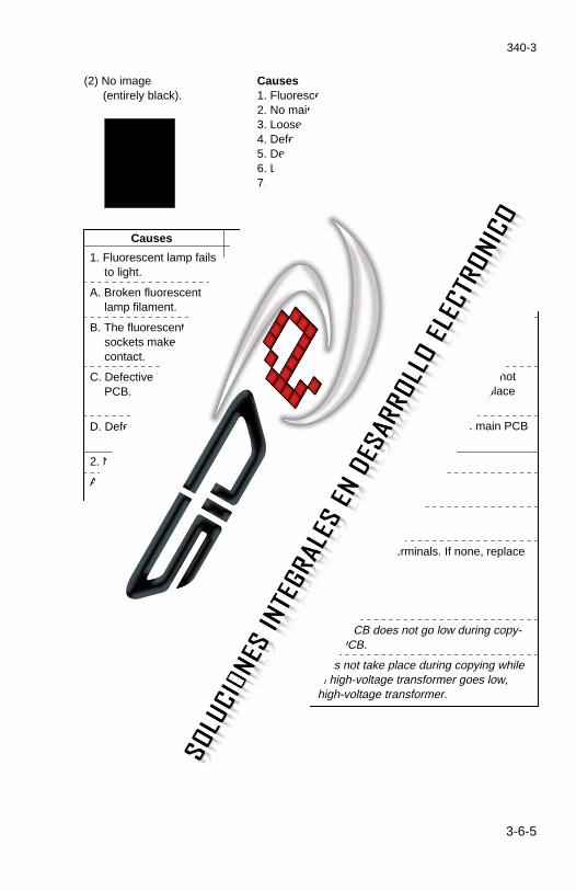
3-6-5
340-3
(2) No image (entirely black).
Causes 1. Fluorescent lamp fails to light. 2. No main charging. 3. Loose LPH data wire connectors. 4. Defective main PCB. 5. Defective LPH. 6.Loose ISU data wire connectors. 7.Defective ISU PCB.
1. Fluorescent lamp fails to light.
A. Broken fluorescent lamp filament.
B. The fluorescent lamp sockets make poor contact.
C. Defective inverter PCB.
D. Defective main PCB.
2. No main charging.
A. Broken main charger wire.
B. Leaking main charger housing.
C. The connector ter-minals of the main high-voltage trans-former make poor contact.
D. Defective main PCB.
E. Defective main high-voltage transformer.
Check for continuity across the fluorescent lamp filament. If none, replace the fluorescent lamp (see page 3-3-19).
Check for continuity across the sockets. If none, replace them.
Run simulation 110 and if the fluorescent lamp does not light while CN1-2 on the inverter PCB goes low, replace the inverter PCB.
Run simulation 110 and check if CN6-18 on the main PCB goes low. If not, replace the main PCB.
Replace the wire.
Clean the main charger housing.
Check for continuity across the terminals. If none, replace them.
If CN6-17 on the main PCB does not go low during copy-ing, replace the main PCB.
If main charging does not take place during copying while CN1-3 on the main high-voltage transformer goes low, replace the main high-voltage transformer.
Causes Check procedures/corrective measures

3-6-6
340-3
(3) Image is too light. Causes 1. Insufficient toner. 2. Deteriorated developer. 3. Dirty or deteriorated drum. 4. Misadjusted fluorescent lamp intensity. 5. Misadjusted developing section. 6. Misadjusted drum surface potential. 7. Dirty LPH. 8. Dirty main charger grid.
1. Insufficient toner.
2. Deteriorated devel-oper.
3. Dirty or deteriorated drum.
4. Misadjusted fluores-cent lamp intensity.
5. Misadjusted developing section.
6. Misadjusted drum surface potential.
7. Dirty LPH.
8. Dirty main charger grid.
If the add toner indicator is lit, replenish toner.
Check the number of copies made with the current devel-oper. If it has reached the specified limit, replace the devel-oper.
Clean the drum or, if the maintenance level has been reached, replace it (see page 3-3-13 or 3-3-10).
Readjust the exposure amount (see page 3-3-24).
Readjust the position of the magnetic brush or doctor blade (see page 3-3-35 or 3-3-33).
Readjust the drum surface potential (see page 3-3-18).
Clean the LPH.
Clean the main charger grid.
Causes Check procedures/corrective measures
3. Loose LPH data wire connectors.
4. Defective main PCB.
5. Defective LPH.
6. Loose ISU data wire connectors.
7. Defective ISU PCB.
Run simulation 159. If no test pattern is output, check the connection of the LPH data wire connectors and remedy if necessary.
Run simulation 159. If no test pattern is output after the LPH data wire connectors have been found to be correctly inserted, replace the main PCB.
Run simulation 159. If no test pattern is output after the LPH data wire connection and main PCB have been confirmed to be fine, replace the LPH.
Run simulation 159. If the test pattern is output, run sim-ulation 121. If the value of each channel is 255, check the connection of the ISU data wire connectors and remedy if necessary.
Run simulation 159. If the test pattern is output, run sim-ulation 121. If the value of each channel is close to 0, re-place the ISU PCB (check that the fluorescent lamp is lit).
Causes Check procedures/corrective measures

3-6-7
340-3
(4) Background is visible. Causes 1. Dirty lens array in the CIS. 2. Deteriorated developer. 3. Misadjusted fluorescent lamp intensity. 4. Misadjusted developing section. 5. Misadjusted drum surface potential. 6. Dirty main charger shield.
1. Dirty lens array in the CIS.
2. Deteriorated devel-oper.
3. Misadjusted
fluorescent lamp intensity.
4. Misadjusted developing section.
5. Misadjusted drum surface potential.
6. Dirty main charger shield.
Clean the lens array in the CIS.
Check the number of copies made with the current devel-oper. If it has reached the specified limit, replace the devel-oper.
Readjust the exposure amount (see page 3-3-24).
Readjust the doctor blade position (see page 3-3-33).
Readjust the drum surface potential (see page 3-3-18).
Clean the main charger shield first with a damp cloth and then with a dry cloth.
Causes Check procedures/corrective measures

3-6-8
340
(5) A white line appears longitudinally.
Causes 1. Dirty or flawed main charger grid. 2. Foreign matter in the developing section. 3. Flawed drum. 4. Dirty contact glass. 5. Dirty middle upper original roller. 6. Dirty LPH.
1. Dirty or flawed main charger grid.
2. Foreign matter in the developing assembly.
3. Flawed drum.
4. Dirty contact glass.
5. Dirty middle upper original roller.
6. Dirty LPH.
Clean the main charger grid. If the wire is flawed, replace it.
Check if the magnetic brush is formed uniformly. If not, replace the developer (see page 3-3-31).
Replace the drum (see page 3-3-10).
Clean the contact glass.
Clean the middle upper original roller.
Clean the LPH.
Causes Check procedures/corrective measures
(6) A black line appears longitudinally.
Causes 1. Dirty contact glass. 2. Dirty lens array in the CIS. 3. Dirty or flawed drum. 4. Deformed or worn cleaning blade. 5. Dirty middle upper original roller. 6. Dirty main charger wire.
1. Dirty contact glass.
2. Dirty lens array in the CIS.
3. Dirty or flawed drum.
4. Deformed or worn cleaning blade.
5. Dirty middle upper original roller.
6. Dirty main charger wire.
Clean the contact glass.
Clean the lens array in the CIS.
Clean the drum or, if it is flawed, replace it (see page 3-3-13 or 3-3-10).
Replace the cleaning blade (see page 3-3-42).
Clean the middle upper original roller.
Clean the main charger wire. If the wire is flawed, replace it (see page 3-3-14).
Causes Check procedures/corrective measures

3-6-9
340-3
(7) A black line appears laterally.
Causes 1. Flawed drum. 2. Dirty developing section.
1. Flawed drum.
2. Dirty developing section.
Replace the drum (see page 3-3-10).
Clean the developing section.
Causes Check procedures/corrective measures

3-6-10
340
(8) One side of the copy image is darker than the other.
Causes 1. Dirty main charger wire. 2. Dirty lens array in the CIS. 3. Defective fluorescent lamp.
1. Dirty main charger wire.
2. Dirty lens array in the CIS.
3. Defective fluorescent lamp.
Clean the main charger wire. If it is extremely dirty, replace it (see page 3-3-14).
Clean the lens array in the CIS.
Run simulation 110 and check the fluorescent lamp. If any problem exists, replace the fluorescent lamp (see page 3-3-19).
Causes Check procedures/corrective measures
(9) Black dots appear on the image.
Causes 1. Dirty or flawed drum. 2. Deformed or worn cleaning blade. 3. Dirty or flawed cleaning fur brush.
1. Dirty or flawed drum.
2. Deformed or worn cleaning blade.
3. Dirty or flawed cleaning fur brush.
Clean the drum or, if it is flawed, replace it (see page 3-3-13 or 3-3-10).
Replace the cleaning blade (see page 3-3-42).
Clean the cleaning fur brush or, if it is flawed, replace it (see page 3-3-46).
Causes Check procedures/corrective measures

3-6-11
340
(10) Image is blurred. Causes 1. Original is conveyed erratically. 2. Deformed press roller. 3. Paper conveying drive system problem.
1. Original is conveyed erratically.
A. Dirty or deformed front upper, middle upper, rear upper, front lower or rear lower original roller(s).
B. Original conveying drive system problem.
C. Original holding section installed incorrectly.
2. Deformed press roller.
3. Paper conveying drive system problem.
Clean or replace any of the front upper, middle upper, rear upper, front lower and rear lower original rollers if necessary.
Check the gears and belts. Grease the gears or readjust the belt tension if necessary (see page 3-3-63).
Reinstall.
Check visually and replace (see page 3-3-52).
Check the gears and belts. Grease the gears or readjust the belt tension if necessary (see pages 3-3-60 and 61).
Causes Check procedures/corrective measures
(11) The leading edge of the image is con-sistently misaligned with the original.
Causes 1. Misadjusted leading edge registration.
1. Misadjusted leading edge registration.
Readjust the leading edge registration (see page 3-3-23).
Causes Check procedures/corrective measures

3-6-12
340-1
(12) The leading edge of the image is spo-radically misaligned with the original.
Causes 1. Registration clutch or bypass registration clutch
installed or operating incorrectly. 2. Original feed clutch installed or operating
incorrectly. 3. Loose original feed drive belt 1.
1. Registration clutch or bypass registration clutch installed or operating incorrectly.
2. Original feed clutch installed or operating incorrectly.
3. Loose original feed drive belt 1.
Check the installation position and operation of each clutch; if it has any operation problem, replace it.
Check the installation position and operation of the original feed clutch. If it has any operation problem, replace the clutch.
Check original feed drive belt 1 and readjust the belt tension (see page 3-3-63).
Causes Check procedures/corrective measures
(13) Paper creases. Causes 1. Paper curled. 2. Paper damp. 3. Misadjusted fixing pressure.
1. Paper curled.
2. Paper damp.
3. Misadjusted fixing pressure.
Check the paper storage conditions.
Check the paper storage conditions.
Check if the fixing unit pressure adjustment nuts are tightened correctly and, if not, remedy.
Causes Check procedures/corrective measures
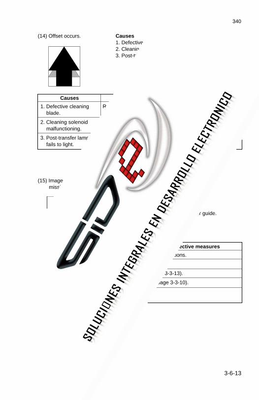
3-6-13
340
(15) Image is partly missing.
Causes 1. Paper damp. 2. Paper creased. 3. Drum condensation. 4. Flawed drum. 5. Deformed pre-transfer inner upper guide.
1. Paper damp.
2. Paper creased.
3. Drum condensation.
4. Flawed drum.
5. Deformed pre-transfer inner upper guide.
Check the paper storage conditions.
Change the paper.
Clean the drum (see page 3-3-13).
Replace the drum (see page 3-3-10).
Remedy or replace.
Causes Check procedures/corrective measures
(14) Offset occurs. Causes 1. Defective cleaning blade. 2. Cleaning solenoid malfunctioning. 3. Post-transfer lamp fails to light.
1. Defective cleaning blade.
2. Cleaning solenoid malfunctioning.
3. Post-transfer lamp fails to light.
Replace the cleaning blade (see page 3-3-42).
Run simulation 45 and if the cleaning solenoid does not operate correctly, replace it.
Run simulation 44 and if the post-transfer lamp does not light, replace it.
Causes Check procedures/corrective measures
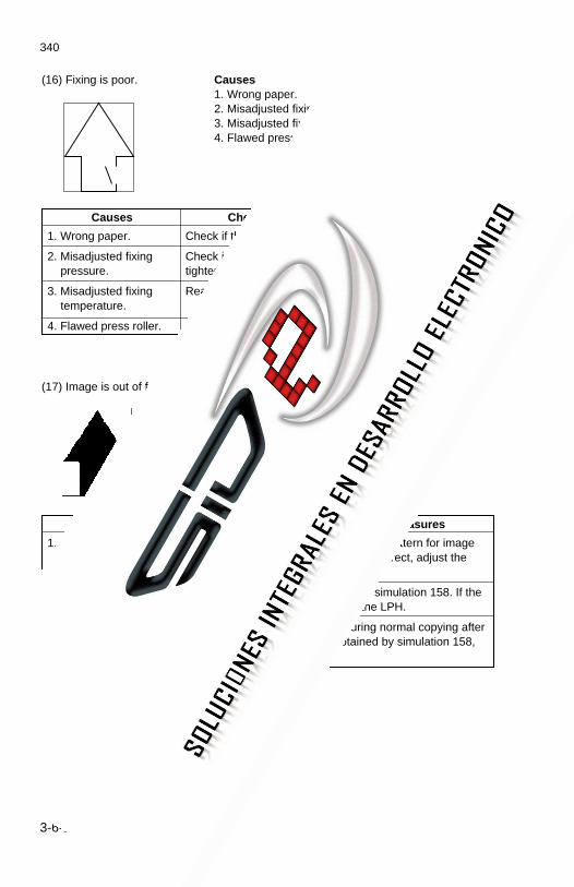
3-6-14
340
(16) Fixing is poor. Causes 1. Wrong paper. 2. Misadjusted fixing pressure. 3. Misadjusted fixing temperature. 4. Flawed press roller.
1. Wrong paper.
2. Misadjusted fixing pressure.
3. Misadjusted fixing temperature.
4. Flawed press roller.
Check if the paper meets specifications.
Check if the fixing unit pressure adjustment nuts are tightened correctly and, if not, remedy.
Readjust the fixing temperature.
Replace the press roller (see page 3-3-52).
Causes Check procedures/corrective measures
(17) Image is out of focus. Causes 1. LPH installed incorrectly. 2. Defective LPH. 3. Defective CIS.
1. LPH installed incorrectly.
2. Defective LPH.
3. Defective CIS.
Run simulation 158 and obtain the test pattern for image focus adjustment. If the image is not correct, adjust the LPH position (see page 3-3-28).
After adjusting the LPH position, run simulation 158. If the test pattern is not correct, replace the LPH.
If the image is still out of focus during normal copying after the correct pattern has been obtained by simulation 158, replace the CIS.
Causes Check procedures/corrective measures

3-6-15
340
(18) The center of the image is misaligned with the original.
Causes 1. Paper roll is not installed correctly on the roll shaft. 2. Paper is not placed correctly on the bypass table. 3. Original is not placed correctly.
1. Paper roll is not installed correctly on the roll shaft.
2. Paper is not placed correctly on the bypass table.
3. Original is not placed correctly.
Correct.
Correct.
Correct.
Causes Check procedures/corrective measures
(19) One forth the A0 width of the image is white.
Causes 1. Defective CIS or ISU PCB. 2. Defective LPH. See (20) One forth the A0 width of the image is black for check procedures and corrective measures.

3-6-16
340-2
(20) One forth the A0 width of the image is black.
Causes 1. Defective CIS or ISU PCB. 2. Defective LPH.
Example If there is a problem with CH1 (CN1) but CH2 (CN2) to CH4 (CN4) are normal, check by swapping the connections of CN1 and CN2 of the CIS and ISU PCB. If the image problem area shifts with the location of CN-1, replace the CIS. If the image problem area doesn't shift, replace the ISU PCB.
1. Defective CIS or ISU PCB.
2. Defective LPH.
Change the connections of CN1, CN2, CN3 and CN4 of the CIS and ISU PCB as shown in the following example to locate the problem.
Run simulation 102. If no gray pattern is output, replace the LPH.
Causes Check procedures/corrective measures

340
3-6-17
(1)J-04 appearsas soon asthe mainswitch isturned on.
(2)J-05 appearsas soon asthe mainswitch isturned on.
(3)J-06 appearsas soon asthe mainswitch isturned on.
A piece of paper torn from copypaper is caught around the by-pass registration roller alongthe paper conveying path.
Defective bypass registrationswitch.
A piece of paper torn from copypaper is caught around theoriginal trailing edge detectionswitch along the paper convey-ing path.
Defective original trailing edgedetection switch.
Roll paper is left uncut.
A piece of paper torn from copypaper is caught around the reg-istration switch, paper convey-ing switch or eject switch alongthe paper conveying path.
Defective registration switch.
Defective paper conveyingswitch.
3-6-2 Paper misfeeds
Problem Causes/check procedures Corrective measures
Check and remove it, if any.
If CN3-14 on the main PCBremains low when the bypassregistration switch is turned onand off, replace the bypass reg-istration switch.
Check and remove it, if any.
If CN3-13 on the main PCBremains low when the originaltrailing edge detection switch isturned on and off, replace theoriginal trailing edge detectionswitch.
Press the job stop/roll cut key tocut remaining paper and re-move it.
Check and remove it, if any.
If CN3-11 on the main PCBremains low when the registra-tion switch is turned on and off,replace the registration switch.
If CN3-15 on the main PCBremains low when the paperconveying switch is turned onand off, replace the paper con-veying switch.

340
3-6-18
(3)J-06 appearsas soon asthe mainswitch isturned on.
(4)Paper jam inthe 1st rollunit (J-01)occurs duringcopying fre-quently.
Defective eject switch.
Wrong paper.
A piece of paper torn from copypaper is left along the paperconveying path between the 1stroll unit and the registrationroller.
Guide plates or other compo-nents along the paper convey-ing path between the 1st rollunit and the registration rollerare deformed.
The roll paper feed upper rollerof the 1st roll unit is dirty withpaper powder.
The roll paper feed upper rollerof the 1st roll unit is deformedor worn.
Broken registration switch ac-tuator.
Defective registration switch.
Electrical problem with the up-per feed clutch.
If CN3-16 on the main PCBremains low when the ejectswitch is turned on and off, re-place the eject switch.
Check and, if the paper is ex-tremely curled or inappropriatefor copying, change it.
Check and remove it, if any.
Check and remedy or replaceany deformed parts.
Check the roll paper feed upperroller and, if it is dirty, clean itwith isopropyl alcohol.
Check and replace the roll pa-per feed upper roller if neces-sary.
Check and, if the actuator isbroken, replace the registrationswitch.
If the level of CN3-11 on themain PCB does not changewhen the registration switch isturned on and off, replace theregistration switch.
See page 3-6-42.
Problem Causes/check procedures Corrective measures

340
3-6-19
(5)Paper jam inthe 2nd rollunit (J-02)occurs duringcopying fre-quently.
(6)Paper jam inthe 3rd rollunit (optional)(J-03) occursduring copy-ing frequently.
Wrong paper.
A piece of paper torn from copypaper is left along the paper con-veying path between the 2nd rollunit and the registration roller.
Guide plates or other compo-nents between the 2nd roll unitand the registration roller aredeformed.
The roll paper feed upper rollerof the 2nd roll unit is dirty withpaper powder.
The roll paper feed upper rollerof the 2nd roll unit is deformedor worn.
Broken registration switch ac-tuator.
Defective registration switch.
Electrical problem with the mid-dle feed clutch.
Wrong paper.
A piece of paper torn from copypaper is left along the paper con-veying path between the 3rd rollunit and the registration roller.
Guide plates or other compo-nents between the 3rd roll unitand the registration roller aredeformed.
The roll paper feed upper rollerof the 3rd roll unit is dirty withpaper powder.
Check and, if the paper is ex-tremely curled or inappropriatefor copying, change it.
Check and remove it, if any.
Check and remedy or replaceany deformed parts.
Check the roll paper feed upperroller and, if it is dirty, clean itwith isopropyl alcohol.
Check and replace the roll pa-per feed upper roller if neces-sary.
Check and, if the actuator isbroken, replace the registrationswitch.
If the level of CN3-11 on themain PCB does not changewhen the registration switch isturned on and off, replace theregistration switch.
See page 3-6-42.
Check and, if the paper is ex-tremely curled or inappropriatefor copying, change it.
Check and remove it, if any.
Check and remedy or replaceany deformed parts.
Check the roll paper feed upperroller and, if it is dirty, clean itwith isopropyl alcohol.
Problem Causes/check procedures Corrective measures
340
3-6-20
(6)Paper jam inthe 3rd rollunit (optional)(J-03) occursduring copy-ing frequently.
(7)Paper jam inthe originalfeed section(J-05) occursduring copy-ing frequently.
The roll paper feed upper rollerof the 3rd roll unit is deformedor worn.
Broken registration switch ac-tuator.
Defective registration switch.
Electrical problem with thelower feed clutch.
Original is extremely curled.
The original is longer than themaximum length.
The surfaces of the front upper,middle upper, rear upper, frontlower or rear lower original roll-ers are dirty with paper powder.
The front upper, middle upper,rear upper, front lower or rearlower original rollers are de-formed or worn.
The original holding section isnot closed completely.
Electrical problem with the origi-nal feed clutch.
Defective original leading edgedetection switch.
Broken actuator of the originalleading or trailing edge detec-tion switch.
Check and replace the roll pa-per feed upper roller if neces-sary.
Check and, if the actuator isbroken, replace the registrationswitch.
If the level of CN3-11 on themain PCB does not changewhen the registration switch isturned on and off, replace theregistration switch.
See page 3-6-43.
Check and correct if necessary.
Use the original whose lengthmeets specifications.
Check and clean any dirty roll-ers with isopropyl alcohol.
Check each roller and, if neces-sary, replace it.
Close the original holding sec-tion completely.
See page 3-6-44.
If CN3-12 on the main PCBdoes not go low when the origi-nal leading edge detectionswitch is turned on and off, re-place the original leading edgedetection switch.
Check the actuator of eachswitch and, if it is broken, re-place the switch.
Problem Causes/check procedures Corrective measures

340
3-6-21
(8)Paper jaminside themain unit (J-06) occursduring copy-ing frequently.
A piece of paper torn from copypaper is left along the paperconveying path between theregistration roller and ejectroller.
Guide plates along the paperconveying path between theregistration roller and the ejectroller are deformed.
Dirty registration, pre-transferand/or eject rollers.
Deformed or worn registration,pre-transfer and/or eject roller.
Extremely dirty press roller orits separation claws.
Deformed press roller or itsseparation claws.
Broken separation charger wire.
Electrical problem with the pa-per conveying fan motor.
Electrical problem with the reg-istration clutch.
Electrical problem with the rollpaper conveying clutch.
Defective paper conveyingswitch.
Defective eject switch.
Check and remove it, if any.
Check and remedy or replaceany deformed guide plates.
Check and clean any dirty roll-ers with the isopropyl alcohol.
Check and replace the roller(s)if necessary.
Check and clean if dirty.
Check and replace if deformed(see page 3-3-52).
Check and replace the separa-tion charger wire if it is broken(see page 3-3-37).
See page 3-6-41.
See page 3-6-43.
See page 3-6-43.
If the level of CN3-15 on themain PCB does not changewhen the paper conveyingswitch is turned on and off, re-place the paper conveyingswitch.
If the level of CN3-16 on themain PCB does not changewhen the eject switch is turnedon and off, replace the ejectswitch.
Problem Causes/check procedures Corrective measures

340
3-6-22
(8)Paper jaminside themain unit(J-06) occursduring copy-ing frequently.
Defective fixing unit pulse sen-sor.
The eject switch actuator or thefixing unit pulse sensor disc isbroken.
If the level of CN3-17 on themain PCB does not changewhen the fixing unit pulse sen-sor is turned on and off, replacethe fixing unit pulse sensor.
Check the actuator and, if it isbroken, replace the ejectswitch. Check the disc and, if itis broken, replace the fixing unitpulse sensor.
Problem Causes/check procedures Corrective measures

340
3-6-23
3-6-3 PCB terminal voltages
Precautions• When handling the circuit boards, do not touch the components wth bare hands.• ICs can be damaged by static discharges. If a PCB contains ICs, do not touch the ICs,
cable connectors or edge connectors.• Store the circuit boards wrapped in aluminum foil, conductive spoge rubber, or similar
material.
(1) Power source PCB
C4C5
4CN1F1T6.3A/250V 1
3402805E1
C3
WA
RN
ING
FO
R C
ON
TIN
UE
D P
RO
TE
CT
ION
AG
AIN
ST
RIS
K
OF
FIR
E. R
EP
LAC
E O
NLY
WIT
H S
AM
E
TY
PE
AN
D R
AT
ING
OF
FU
SE
.
C2
L3
R1
L2C1
SQ
2
L1
SQ
3SQ
1
R7
+
+
TP
2
C13
R15
R8
C9
L5 D3R5 D1 ~ ~
C8
T1 CR1
R2
JP1
D2
L13R10
S Q1
R12JP4
C12
R11
R14
D5 Q2 5
JP3
L4
SG
Q3
S
R18
G
Q4
C14
S
G
R3
C7
GR16
JP5JP6
JP7JP8JP9
JP10
JP11
R44R43R42
C25
R40R41
R37R36
R39 R28
R32
R23
C17 C16R17
WH1 R01
R24
R26
101 C55R45
D10TS1
Z4
Z2
RC
D11R33
C26
C22
C23
JP15
JP33
Z9U2
1 1D28
D33
R76
C53
R73JP25R68 JP15
JP26C48
R56R55
Z11
C35
C39
CN2
CN4
CN3
C40
41
1 7
91
C37
R60 L14 D17 R61 Q5
C41
C42
L13
D16R63
L15
D18R64
ID20
Z7D22O D19 Z8
D21I O
C46
C47
CN7
L17
31
CN6
CN51 8
81 JP30
CR
R85R80
R57
R52
L10
L6 D12L7
C32
R47
C31R48
D13
L8 L9C33
R49
RD2 WH2
L11
D27R69R70R74
R71R75
R79R77R78
R82R81
Z10
R50JP21
D24 C28
R46
C27
C22
C23
C24
+R
29
R30JP
13JP12
R31
TP
1
RV
1
JP14
Z1
R34
R35
R90
R38
R91
Z5
++ 14
1
+
1Z
3
C15
D6
D8
C21
1
R25
R27
D9
C20 +
JP17
JP34
+
C18
6
7
5000949E
111
12
JP16
PS
C10
D7
R20
R22
JP32
R19
+
R5
R4
R13
C11
D4
R9
R21
C57
C56
C6
++
C19R
66JP
19JP
20
JP24
D26
D25
R72
D29 JP
27D
30D
32 D31
RV
2
JP18
C49
C51
R88
C50
C52
1Z12
R84
R87
R86
R89
R83
JP28
RC
C36
Z6
R54
D14
D15
R53
R51
+
+
++
R59
JP29
C38L12
C29
C30
C34 Y
EC
L19
C54 U
31
7
L15JP
31
R62
+
C43
C45
+
C44+
+
R65
D23
+
600878L-B U
1M
AD
E IN
JAP
AN
FS
-5V
-
C4C5
4CN1F1T10A/125V 1
3402804E1
C3
WA
RN
ING
FO
R C
ON
TIN
UE
D P
RO
TE
CT
ION
AG
AIN
ST
RIS
K
OF
FIR
E. R
EP
LAC
E O
NLY
WIT
H S
AM
E
TY
PE
AN
D R
AT
ING
OF
FU
SE
.
C2
L3
R1
L2C1
SQ
2
L1
SQ
3SQ
1
R7
+
+
TP
2
C13
R15
R8
C9
L5 D3R6 D1 ~ ~
C8
T1 CR1
R2
JP1
D2
L18R10
S Q1
R12JP4
C12
R11
R14
D5 Q2 G
JP3
L4
SG
Q3
S
R18
G
Q4
C14
S
G
R3
C7
GR16
JP5JP6
JP7JP8JP9
JP10
JP11
R44R43R42
C25
R40R41
R37R36
R39 R23
R32
R23
C17 C16R17
WH1 R01
R24
R26
101 C55R45
D10TS1
Z4
Z2
RC
D11R33
C26
C22
C23
JP22
JP33
Z9U2
1 1D28
D33
R76
C53
R73JP25R68 R67
JP26C48
R56R55
Z11
C35
C39
CN2
CN4
CN3
C40
41
1 7
91
C37
R60 L14 D17 R61 Q5
C41
C42
L13
D16R63
L15
D18R64
ID20
Z7D22O D19 Z8
D21I O
C46
C47
CN7
L17
31
CN6
CN51 8
81 JP30
CR
R85R80
R57
R52
L10
L6 D12L7
C32
R47
C31R48
D13
L8 L9C33
R49
RD2 WH2
L11
D27R59R70R74
R71R75
R79R77R78
R82R81
Z10
R50JP21
D24 C28
R46
C27
C23
C23
C24
+R
29
R30JP
13JP12
R31
TP
1
RV
1
JP14
Z1
R34
R35
R90
R38
R91
Z5
++ 14
1
+
1Z
3
C15
D6
D8
C21
1
R25
R27
D9
C20 +
JP17
JP34
+
C18
6
7
5000855E
111
12
JP16
PS
C10
D7
R20
R22
JP32
R19
+
R5
R4
R13
C11
D4
R9
R21
C57
C56
C6
++
C19R
66JP
19JP
20
JP24
D26
D25
R72
D29 JP
27D
30D
32 D31
RV
2
JP18
C49
C51
R88
C50
C52
1Z12
R84
R87
R86
R89
R83
JP28
RC
C36
Z6
R54
D14
D15
R53
R51
+
+
++
R59
JP29
C38L12
C29
C30
C34 Y
EC
L19
C54 U
31
7
L15JP
31
R62
+
C43
C45
+
C44+
+
R65
D23
+
6000728L-C U
1M
AD
E IN
JAP
AN
FS
-5V
-
220 – 240 V area 120 V area

340
3-6-24
Terminals (CN) Voltage Remarks
1-1 1-4 Local voltage AC supply, input
2-1 2-4 24 V DC 24 V DC supply, output
3-1, 2, 3, 4 3-5, 6, 7, 8 24 V DC 24 V DC supply, output
4-1, 2, 3, 4 4-5, 6 24 V DC 24 V DC supply, output
5-1, 2, 3 5-5, 6, 7 5 V DC 5 V DC supply, output
6-1, 2, 3, 4 6-5, 6, 7, 8 5 V DC 5 V DC supply, output
7-1 7-2 +12 V DC +12 V DC supply, output
7-3 7-2 –12 V DC –12 V DC supply, output
MADE IN JAPAN 7000267L-C U-2
C5
R14
R17R18C8
C7
C6R11
R12R10
R1
R7
R2
C2
R6 Z1
R3
R9
110
R4
D1
1
JP1C
N1
D2
JP2
C9
R15
R16
RV
1
C3
C1
R5
R8
JP3
D1 FS-1V
C4
R13
+
+
1
YEC
MADE IN JAPAN
7000268L-B
C4
C3
C8
R7
R8FS-1V
R12R10
+
YEC
R16
R5R4
C7
R6
R13 C6
R11
R17
R18
R19
D1
D2
R2
R1
JP1
R15
U-3
R9
CN11 7
Q1
C1
Z1 1
R3
Z2D3 RV1
C2
1
C5 R14

340
3-6-25
(2) LPH power source PCB
Terminals (CN) Voltage Remarks
A-1 A-3 24 V DC 24 V DC supply, input
B-1 B-5, 6, 7, 8 5 V DC 5 V DC supply to LPH, output
B-2 B-5, 6, 7, 8 5 V DC 5 V DC supply to LPH, output
B-3 B-5, 6, 7, 8 5 V DC 5 V DC supply to LPH, output
B-4 B-5, 6, 7, 8 5 V DC 5 V DC supply to LPH, output
MADE IN JAPAN3402806
YEC 6000727L-C
C26
C7
D4
C2
L1
R1
R19
R18
R9
C4 C3+ ++
R10
R7
R5
R15
JP1
R17
R13
C13C11 C
22
C10R12
R23
R26
R22
R21
R27
R30
R3
R11
R2
R31
R29
R32
R20
C24
JP3
R25
R24
R4
Z2
D6T1D7
C9
Z3
C20
C21
C19
CN8
C25
L5
81
1 1
R28
R CZ4
C12R14
C14
D8
CNV
RV11 2
R16
R6
SG
Q1
D3
Z1
C23
RC
Z5
D10
JP2
++
+
+
+
+ L2
C18
C16
C17
C28
C27
D1
F1 10A/125V
WARNING
FOR CONTINUED PROTECTION AGAINST RISK OF FIRE,REPLACE ONLY WITH SAME TYPE AND RATING OF FUSE.
3 1CNA
5
1
7
12
C15
L3L4
D9
TS
1
JP4
C6
R8 D
2
C1
C5
D5
D8 R
DW
H

340
3-6-26
(3) Main PCB
IC34
ALS
197
IC35
ALS
192
IC51
ALS
192
IC68
ALS
192
IC69
ALS
192
IC81
ALS
192
IC90
F24
5
IC91
F24
5
IC10
1 F
245
IC10
9
F24
5
IC18
A
LS19
2
CO
N19
CO
N20
IC12
A
LS19
2
IC13
A
LS19
2
IC23
A
LS19
7
IC43
U
PD
4228
0GU
IC44
U
PD
4228
0GU
IC24
F
374
IC25
A
C14
IC26
F
74
BS
8IC
14 A
LS19
2IC
15 A
LS19
7IC
16 A
LS19
2IC
27
F04
IC29
LS
07IC
29
ALS
192
IC30
A
LS19
7IC
31
ALS
197
IC32
A
LS19
7IC
33
ALS
192
IC45
F
374
IC46
F
04IC
47
HC
14IC
49
ALS
192
IC50
A
LS19
2
IC62
F
374
IC63
F
74IC
65
F04
IC66
F
157
IC48
A
LS19
7B
S9
BS
5
IC84
C
Y7C
185A
IC88
C
Y7C
185A
IC10
6 T
CS
5328
BJ
IC89
H
DC
G43
IC87
C
Y7C
185A
IC78
U
PD
4855
05G
IC87
C
Y7C
185A
IC79
CY
7C18
5AIC
80 C
Y7C
185A
RA
5
RA
10
RA
6R
A7
IC42
UP
D42
280G
U
IC60
UP
D42
280G
U
BS
4 B
S3
RA
12
RA
17
IC100
CH
TG
43R
A24
BS
12
CO
N21
BS
10 B
S11
X3
RA
11
IC77
F
245
IC85
F
245
IC97
F
04IC
86
F24
5
IC94
T
CZ
03
IC86
F
245
IC61
F
ILL1
7
IC12
1 LN
CG
43
IC18
7 F
245
CON22
RA
15
RA
20
RA
21
RA
22
RA
23
RA
18
RA
13
RA
14 RA
19
RA
29
RA
16
NF
357
NF
283 12
0NF
358
NF
359
NF
310
NF
315
NF503
NF
360
NF
285
81
108109
144
NF502
7372
37
36 1
208
1
NF135 NF138 NF160 NF184 NF185 NF209 NF250
NF247
NF248NF208
NF183
NF155
NF158
NF159
NF154
NF89
NF88
NF87
NF85
NF84
NF150
NF151NF177
NF205
NF245
NF152
NF153
NF181
NF182
NF207
NF206
NF246
NF282
NF284
A30
B30
B1 B16
A16 A1B1
A1A1
B1
NF
249
105
156
157
104
53
52
11
11111111
111
9999999
1 1 1 1 1 11
1515
15 15
1 1
111
13
1
11
11
1
11
11
111
11
11
118
89
1
99
99
118
8
89
999
99
99
9
11
11
1
1515
15
1
11
11
11
1
11
98
88
NF
180
158
157
104
105
208
52
53
11
11
15
1
NF
244
1111
1
11
11
81
88
NF
281
51
50 3118
8
1
8
30
A1
B30
A30 B1
51
52
1 2
99
100
49
50
NF90NF91
DI9
DI7DI6
K A C
K A C
K A C
C
C
C
C
C
K A
K A
K A
K A
K A
C
K A
C
K A
C
K A
C
K A
DI10
DI12
DI14
DI16DI15
DI18DI17
DI13
DI11
NF93 NF94
NF99
NF102NF103
NF97
NF101
NF105
NF92
NF98
NF120 NF122 NF124 NF126 NF128 NF130 NF132 NF134
NF26 NF27 NF29 NF31 NF33 NF34 NF36 NF37 NF38 NF39 NF40 NF41 NF43 NF45 NF46 NF48 NF49 NF51 NF52 NF53 NF55 NF57 NF58 NF60
NF
137
NF
138
NF
139
NF
140
NF
141
NF
142
NF
161
NF
162
NF
163
NF
164
NF
105
NF
166
NF
186
NF
187
NF
188
NF
189
NF
143
NF
144
NF
145
NF
146
NF
167
NF
168
NF
169
NF
170
NF
171
NF
172
NF
193
NF
194
NF
195
NF
196
NF110 NF121 NF123 NF125 NF127 NF129 NF131 NF133
NF73 NF74 NF75 NF76 NF77 NF78 NF79 NF80
NF
190
NF
191
NF
192
NF
210
NF
197
NF
198
NF
199
NF
216
NF
211
NF
212
NF
213
NF
214
NF
217
NF
218
NF
219
NF
220
NF
215
NF
253
NF
254
NF
255
NF
221
NF
258
NF
259
NF
260
1515
NF
251
NF
252
NF
286
NF
287
NF
289Z
N
F29
0Z
NF
291Z
N
F28
9 N
F31
6 N
F31
7 N
F31
8 N
F31
9 N
F30
3Z
NF
320
NF
256
NF
257
NF
290
NF
291
NF
292
NF
292Z
N
F29
3Z
NF
288
NF
295
NF
321
NF
322
NF
323
NF
324
NF
304Z
N
F30
5Z
NF396 NF398 NF399 NF400 NF401 NF402 NF403 NF404 NF405 NF406 NF407 NF408 NF410 NF411
IC10
8 A
LS19
7
IC12
5 A
LS19
7
IC12
6 A
LS19
7IC
124
F37
4
IC16
0 F
74
IC15
8 A
LS19
7
IC15
5 A
LS19
2IC
157
ALS
197
IC15
9 A
LS19
2
IC16
1 LS
07
IC15
6 A
LS19
7
ALS
192
IC11
4 U
PD
4855
05G
IC11
5 A
LS19
2
IC14
2 F
04
IC14
0 F
74
IC15
4
IC14
1 F
04
IC11
3 T
C55
328B
J
BS
2
IC12
3 T
C55
328B
J
IC12
2 T
C55
328B
J
IC13
9 T
C55
328B
J
IC13
8 T
C55
328B
J
IC15
2 U
PD
4288
0GU
IC13
7 T
C55
328B
J
RA
34
BS
1
CO
N18
CON17
A17
B17
IC15
3 F
374
IC15
1 F
374
IC16
2 F
374
RA
42
IC10
5 Y
C55
3288
JIC
104
CY
7C18
5A
IC13
6 T
C55
328B
J
IC150 AEPG43RA36
RA37
IC11
2
IUP
G43
C16
7C
170
CO
N5
••
••
••
••
••
•6
78DE
C 2
2V-O
YS
D-E
0005
10-0
01-A
RA
061Z
RA
48R
A46
RA
45R
A44
RA
062Z
8
1A
1
B1
11
11
1
11
98
9
99
A50
B50
11
1
1
1
1
NF
446
RA
064Z
RA
063Z
120
91
90
1
7
+
NF
394
RA
26N
F38
6
NF
352
NF
354
NF353
NF351NF350
31
60
30
13
1
15
361
144 109 108
15
1
60
61
91
90
19
31
37 72
73
NF395
NF392
NF393
NF432
NF433
NF412NF375 NF413
NF414
NF416
NF419NF421
NF422NF377 NF031Z
NF364
NF423
NF415 NF417 NF418 NF420
NF374NF361
1515
11
11
1115
1515
11
NF
397
NF
409
NF
373
4816
01
41
8012
1
1 1 1 1
15 1 15
15
1
15
9
9
9
9
8
1111
1
15
131
88
11
99
NF
380
NF
427
NF
381
NF
439
IC41
1Z
UP
C35
8G2
BS
103
IC22 M3881M2-061FP
CON16
CON15
IC53
F
32
IC75
F
245
IC95
F
373
IC94
F
245
IC96
F
373
IC76
F
245
IC56
F
138
IC54
F
04IC
58
F32
IC55
F
32IC
57
F32
IC59
F
32
IC74
C
XK
5825
7BM
-70L
L
IC84
C
XK
5825
7BM
-70L
LIC
83
M27
C40
02-1
20
IC93
M
27C
4700
2-12
0
IC4
HC
4052
IC6
M62
354P IC
41
N14
0115
0A
IC35
1Z
UP
C35
8G2
CO
N2
CO
N1
3402
801
RE
V:1
CON3 CON7 CON8
IC36
1Z
HC
14IC
2 H
C39
3IC
1 H
C14
IC38
H
C39
3
IC52
H
C14
IC72
LS
07
IC71
LS
07
IC82
LS
07
IC92
LS
07
IC40
1Z
UP
C35
8G2
IC37
LS
07IC
19
LS07
UP
C39
3 IC
3
TC
7W14
F
IC20
IC39
HC
32IC
40H
C08
C16
C22
X1
11
1
1111
11
NF298 NF299 NF300 NF301
NF302 NF303 NF304 NF305
NF228 NF229 NF230 NF231
NF232 NF233 NF234 NF235 NF236
NF237 NF238 NF239 NF240 NF241 NF242 NF243
NF265
NF266
NF267
NF268
NF269
NF270
NF271
NF272
NF273
NF274
NF275
NF277
NF278
NF279
NF280
NF276
CP58
NF227
NF204
NF173
NF176
CP44
2121
1
15
1111
1
11
1
88
9
11
11
15
88
88
NF
175
NF
174
NF
147
NF
148
NF
149
6564
80
24
25
4041
1
1
5
1 2
5 6
TP
1716
64
49
1
2 20
19
483332
1
12
2122
DI5K
A C
++1
2
8
59
58
8
8 8
8 8 8 8 8 8
5
88
9
DI1
DI2
1 2
19 20
11
11
11
1
5
1 111
DI8
KA C
KA C
3334
12
2324
12
78
12
NF226 NF264
DI10
1 1 1 1 1 1
1 1
1
RA
33
IC103ZMCG43
IC11
1 M
3770
2S1A
FP
IC11
9 H
C14
IC13
0 H
C08
IC13
1 H
C74
IC13
3 T
D62
382
IC14
8 T
D62
308
IC14
7 T
D62
382
IC14
4 T
D62
382
IC33
1Z
TD
6238
2
IC11
6 LS
07IC
117
HC
14
IC33
2Z
TD
6238
2
IC14
6 T
D62
308
IC12
7 T
D62
308
IC12
8 T
D62
308
IC14
5 T
D62
308
IC14
9 T
D62
308
IC13
4 T
D62
308
IC13
5 T
C55
328B
J
IC11
8 T
A80
30F
IC1A
H
C02
TR10TR18
TR14
L4
L5
TR19
TR20
TR16
TR13
TR2
CON14
CON13
TR4
TR001E
TR6
TR7
TR5
TR3L1
L2
C163
C137
BS104
IC110
CON10
IC102 N1401150A
TR9
X2
BS13
NF297
NF296
NF326
NF325NF367
DI001E
A1
B1
A10
B10
ECB
ECB
BCEA10B10
A1B1
40
2524 1
80 4948 33
32
1716
641
65
A1A2
B1B2
A15A14
B15B14
6441
TR11
TR12
C12
5
IC13
2 LB
1651
CO
N6
CO
N4
CO
N11
TR
8
X4
M3881M2-061FP
RG
001E
NF327
NF328
NF329
NF331
NF332
NF333
NF334
NF335
NF336
NF337
NF338
NF339
NF340
NF341
NF342
NF343
NF345
NF346
NF347
NF348
NF
344
NF
370
NF
371
NF
372
NF349 NF391
NF390
25
120
1 30
41
40
24
164 65
NF
330
NF
368
11
58+
80
1
+
11
188
4
DI2
0 DI004E DI002E DI003E
DI005E
TR15
DI24
DI26
DI25
DI29 DI30
B
6
CE
B
DI23
DI27
DI28
B
B
C
C
E
E
DI33 DI34
DI331Z
DI31
DI21
DI32
CE
B
EC
99
11
10
11
1
99
1
A17
B17
A1
B1
1912
20
1
10
DI2
2
99
11 1
1
1110
9
RA
002E
RA
001E
RA
003E
RA
421Z
RA
422Z
RA
424Z
RA
423Z
RA
004E
10
8
1
1
11
88
OG
I10
1 81
KA
KA
A
A
A
EB
C
EB
C
EB
C
EB
C
EB
C
KA C
EB
C
EB
EB
C
EB
C
EB
C
C
C
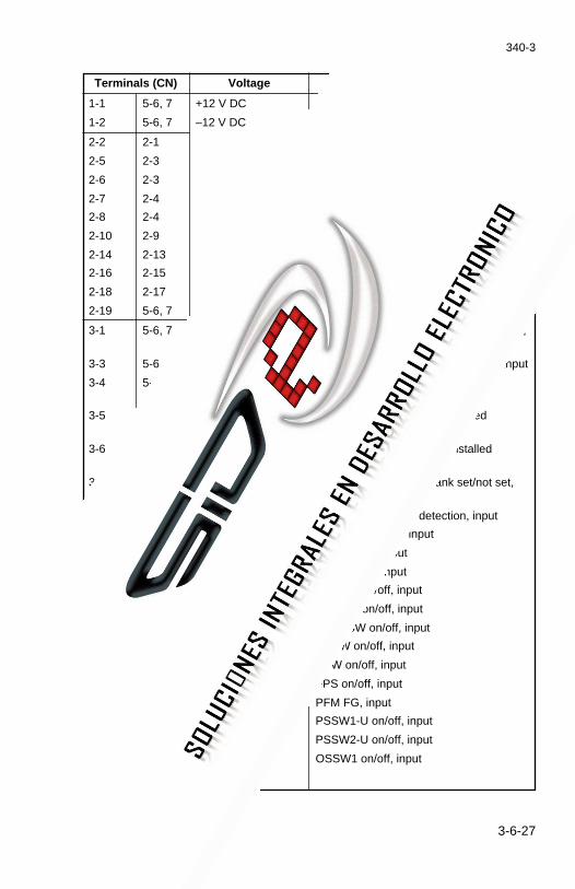
340-3
3-6-27
Terminals (CN) Voltage Remarks
1-1 5-6, 7 +12 V DC +12 V DC supply, input
1-2 5-6, 7 –12 V DC –12 V DC supply, input
2-2 2-1 DTH detection, input
2-5 2-3 FTH1 detection, input
2-6 2-3 FTH2 detection, input
2-7 2-4 FTH3 detection, input
2-8 2-4 FTH4 detection, input
2-10 2-9 ETTH detection, input
2-14 2-13 FLTH detection, input
2-16 2-15 DPS detection, input
2-18 2-17 TNS detection, input
2-19 5-6, 7 DB control, output
3-1 5-6, 7 0/5 V DC KC*1 connected/not connected detection,input
3-3 5-6, 7 0/5 V DC Transfer charger shorting detection, input
3-4 5-6, 7 0/5 V DC 1st roll unit installed/not installeddetection, input
3-5 5-6, 7 0/5 V DC 2nd roll unit installed/not installeddetection, input
3-6 5-6, 7 0/5 V DC 3rd roll unit*1 installed/not installeddetection, input
3-7 5-6, 7 0/5 V DC TDTDSW waste toner tank set/not set,input
3-8 5-6, 7 5/0 V DC OFS toner overflow detection, input
3-9 5-6, 7 5/0 V DC RLDSW-U on/off, input
3-10 5-6, 7 0/5 V DC (pulse) PS-U on/off, input
3-11 5-6, 7 0/ 5V DC RSW on/off, input
3-12 5-6, 7 0/5 V DC OLDSW on/off, input
3-13 5-6, 7 0/5 V DC OTDSW on/off, input
3-14 5-6, 7 5/0 V DC BYPRSW on/off, input
3-15 5-6, 7 0/5 V DC PCSW on/off, input
3-16 5-6, 7 5/0 V DC ESW on/off, input
3-17 5-6, 7 0/5 V DC (pulse) FPS on/off, input
3-18 5-6, 7 0/5 V DC (pulse) PFM FG, input
3-19 5-6, 7 0/5 V DC PSSW1-U on/off, input
3-20 5-6, 7 0/5 V DC PSSW2-U on/off, input
3-21 5-6, 7 0/5 V DC OSSW1 on/off, input
*1 Optional
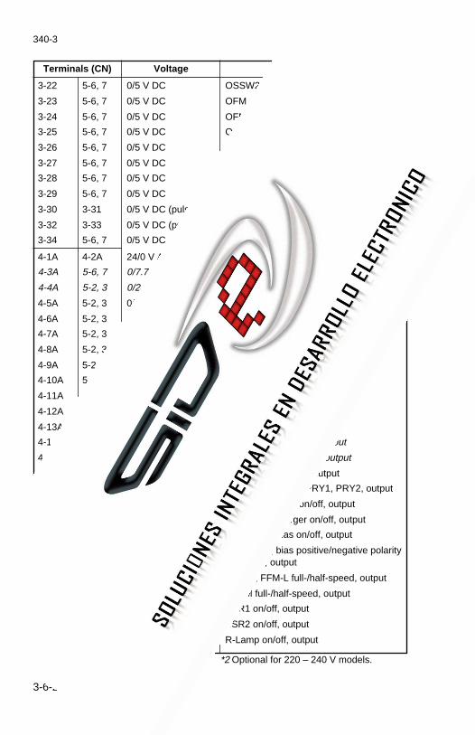
340-3
3-6-28
Terminals (CN) Voltage Remarks
3-22 5-6, 7 0/5 V DC OSSW2 on/off, input
3-23 5-6, 7 0/5 V DC OFM SPEED1, output
3-24 5-6, 7 0/5 V DC OFM ENA, output
3-25 5-6, 7 0/5 V DC OFM SPEED2, output
3-26 5-6, 7 0/5 V DC PFM SPEED1, output
3-27 5-6, 7 0/5 V DC DCM2PCB RESET, output
3-28 5-6, 7 0/5 V DC PFM SPEED2, output
3-29 5-6, 7 0/5 V DC PFM ENA, output
3-30 3-31 0/5 V DC (pulse) DCM2PCB serial communication, input
3-32 3-33 0/5 V DC (pulse) DCM2PCB serial communication, output
3-34 5-6, 7 0/5 V DC BYPTIMSW on/off, input
4-1A 4-2A 24/0 V AC TM on/off, output
4-3A 5-6, 7 0/7.7 V DC SSR3*1 on/off, output
4-4A 5-2, 3 0/24 V DC Auto shutoff on/off, output
4-5A 5-2, 3 0/24 V DC FFM-R, FFM-L on/off, output
4-6A 5-2, 3 0/24 V DC PCFM on/off, output
4-7A 5-2, 3 0/24 V DC OFCL on/off, output
4-8A 5-2, 3 0/24 V DC FCL-U on/off, output
4-9A 5-2, 3 0/24 V DC RWCL-U on/off, output
4-10A 5-2, 3 0/24 V DC KC count on/off, output
4-11A 5-2, 3 0/24 V DC TC count on/off, output
4-12A 5-2, 3 0/15.5 V DC PCHL on/off control, output
4-13A 5-2, 3 0/15.5 V DC DH on/off control, output
4-14A 5-2, 3 0/24 V DC RH-U*2 on/off control, output
4-15A 5-2, 3 0/24 V DC RH-L*2,3 on/off control, output
4-16A 5-2, 3 0/2.7 V DC PRY1, PRY2 on/off, output
4-17A 5-2, 3 24 V DC 24 V DC supply to PRY1, PRY2, output
4-1B 5-2, 3 0/24 V DC Transfer charger on/off, output
4-2B 5-2, 3 0/24 V DC Separation charger on/off, output
4-3B 5-2, 3 0/24 V DC Developing bias on/off, output
4-4B 5-2, 3 0/24 V DC Developing bias positive/negative polarityswitching, output
4-5B 5-2, 3 0/5.5 V DC FFM-R, FFM-L full-/half-speed, output
4-6B 5-2, 3 0/4.8 V DC PCFM full-/half-speed, output
4-7B 5-6, 7 0/7.7 V DC SSR1 on/off, output
4-8B 5-6, 7 0/7.7 V DC SSR2 on/off, output
4-9B 5-2, 3 0/18.7 V DC R-Lamp on/off, output
*1 For 230 V, 50 Hz models only. *2 Optional for 220 – 240 V models.*3 Optional for 120 V models.
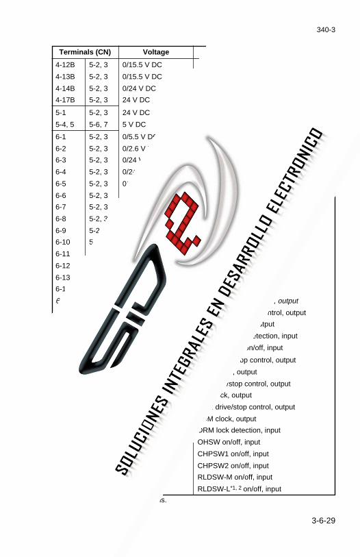
340-3
3-6-29
Terminals (CN) Voltage Remarks
4-12B 5-2, 3 0/15.5 V DC RTL on/off control, output
4-13B 5-2, 3 0/15.5 V DC FLH on/off control, output
4-14B 5-2, 3 0/24 V DC RH-M*1 on/off, output
4-17B 5-2, 3 24 V DC 24 V DC supply, input
5-1 5-2, 3 24 V DC 24 V DC supply, input
5-4, 5 5-6, 7 5 V DC 5 V DC supply, input
6-1 5-2, 3 0/5.5 V DC LPHFM1 full/half-speed, output
6-2 5-2, 3 0/2.6 V DC CFM full-/half-speed, output
6-3 5-2, 3 0/24 V DC CFM on/off, output
6-4 5-2, 3 0/24 V DC CSOL hold/off, output
6-5 5-2, 3 0/24 V DC CSOL pull/off, output
6-6 5-2, 3 0/24 V DC SSOL on/off, output
6-7 5-2, 3 0/24 V DC RCL on/off, output
6-8 5-2, 3 0/24 V DC CCL on/off, output
6-9 5-2, 3 0/24 V DC RPCCL on/off, output
6-10 5-2, 3 0/24 V DC FCL-M on/off, output
6-11 5-2, 3 0/24 V DC RWCL-M on/off, output
6-12 5-2, 3 0/24 V DC FCL-L*1, 2 on/off, output
6-13 5-2, 3 0/24 V DC RWCL-L*1, 2 on/off, output
6-14 5-2, 3 0/24 V DC BYPRCL on/off, output
6-15 5-2, 3 0/5.5 V DC LPHFM2 full/half-speed, output
6-17 5-2, 3 0/24 V DC Main chager on/off control, output
6-18 5-2, 3 0/24 V DC FL on/off control, output
6-19 5-6, 7 0/5 V DC MHVT shorting detection, input
6-20 5-2, 3 24/0 V DC SSW1, SSW2 on/off, input
7-1 5-6, 7 0/5 V DC DRM drive/stop control, output
7-2 5-6, 7 0/5 V DC (pulse) DRM clock, output
7-4 5-6, 7 0/5 V DC DM drive/stop control, output
7-5 5-6, 7 0/5 V DC (pulse) DM clock, output
7-6 5-6, 7 0/5 V DC FDM drive/stop control, output
7-7 5-6, 7 0/5 V DC (pulse) FDM clock, output
7-8 5-6, 7 0/5 V DC DRM lock detection, input
7-11 5-6, 7 0/5 V DC OHSW on/off, input
7-12 5-6, 7 5/0 V DC CHPSW1 on/off, input
7-13 5-6, 7 5/0 V DC CHPSW2 on/off, input
7-14 5-6, 7 0/5 V DC RLDSW-M on/off, input
7-15 5-6, 7 0/5 V DC RLDSW-L*1, 2 on/off, input
*1 Optional for 220 – 240 V models.*2 Optional for 120 V models.
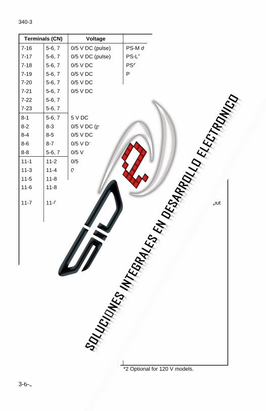
340-3
3-6-30
Terminals (CN) Voltage Remarks
7-16 5-6, 7 0/5 V DC (pulse) PS-M detection, input
7-17 5-6, 7 0/5 V DC (pulse) PS-L*1, 2 detection, input
7-18 5-6, 7 0/5 V DC PSSW1-M on/off, input
7-19 5-6, 7 0/5 V DC PSSW2-M on/off, input
7-20 5-6, 7 0/5 V DC PSSW1-L*3 on/off, input
7-21 5-6, 7 0/5 V DC PSSW2-L*3 on/off, input
7-22 5-6, 7 FL light intensity control, output
7-23 5-6, 7 Grid control, output
8-1 5-6, 7 5 V DC 5 V supply to OPCB, output
8-2 8-3 0/5 V DC (pulse) OPCB serial communication, input
8-4 8-5 0/5 V DC (pulse) OPCB serial communication, output
8-6 8-7 0/5 V DC (pulse) OPCB clock, output
8-8 5-6, 7 0/5 V DC Job stop/roll cut key on/off, input
11-1 11-2 0/5 V DC (pulse) ISUPCB serial communication, input
11-3 11-4 0/5 V DC (pulse) ISUPCB serial communication, output
11-5 11-8 0/5 V DC ISUPCB reset, output
11-6 11-8 0/5 V DC ISUPCB connected/not connecteddetection, input
11-7 11-8 FL light intensity feedback control, input
*1 Optional for 220 – 240 V models. *2 Optional for 120 V models.*3 Optional
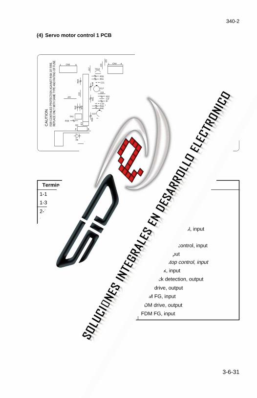
340-2
3-6-31
(4) Servo motor control 1 PCB
Terminals (CN) Voltage Remarks
1-1 1-2 24 V DC DM drive, output
1-3 1-4 0.5 V AC (sinusoidal) DM FG, input
2-1 2-2 24 V DC 24 V DC supply, input
2-4 2-5 5 V DC 5 V DC supply, input
3-1 2-5 0/5 V DC DM drive/stop control, input
3-2 2-5 0/5 V DC (pulse) DM clock, input
3-3 2-5 0/5 V DC FDM drive/stop control, input
3-4 2-5 0/5 V DC (pulse) FDM clock, input
3-5 2-5 0/5 V DC DRM drive/stop control, input
3-6 2-5 0/5 V DC (pulse) DRM clock, input
3-7 2-5 0/5 V DC DRM lock detection, output
4-1 4-2 24/0 V DC (pulse) DRM drive, output
4-3 4-4 0.5 V AC (sinusoidal) DRM FG, input
5-1 5-2 24/0 V DC (pulse) FDM drive, output
5-3 5-4 0.5 V AC (sinusoidal) FDM FG, input
CA
UT
ION
FOR
CONT
INUE
D PR
OTE
CTIO
N AG
AINS
T RI
SK O
F FI
RE.
REPL
ACE
ONL
Y W
ITH
SAM
E TY
PE A
ND R
ATIN
G O
F FU
SE.
DMCP
-050
-A15
E-
0757
A 34
0280
8
CN5 CN3 CN2CN4 CN1
C2
+J2
J1
C3
1 4 1 4 7 1 1 4 5 1
J7J8
J15
J16
J17
J19
J14
CX
2J1
3
R49
R43 R24
R28
R29
R6
R7
R23
R20
C11
C15
J12
R22
R39
R48
R47
TR
12
R41
R40
R30
R21
R57
R56
R13
R4
R5
R3
J4
125V
6.3A
F1C
X1
J5
IC3
IC2
R42
J20
J18
J11
+
+
+
+
+TP3
R38
R37
J23
R18
Q3 Q2
E B E B
IC1
Q1
E B
D6 D5 D3
R1
D1D4 D2
J22 +C1
J21
R50R51
R53R58
R19
R52C20
C19R44R45
R46
TR13
C17
C22
C21
TR14
TP2
TR11
C10
C14R31R32
TR6
TR10
J9J10
C16R35
R33R27
R25R26
R34R35 R2
C12
TR7
TR5
TR9
C13
J6
TP1
+R14R15
R3C7
C6
J3
R10
R17
R54
TR3
R8R9
C5
TR2
TR1
C4
C8
+

340
3-6-32
(5) Servo motor control 2 PCB
Terminals (CN) Voltage Remarks
1-1 1-4, 5 24 V DC 24 V DC supply, input
1-2 1-4, 5 24 V DC 24 V DC supply, input
1-3 1-6 5 V DC 5 V DC supply, input
2-1 1-6 0/5 V DC OFM SPEED1, input
2-2 1-6 0/5 V DC OFM ENA, input
2-3 1-6 0/5 V DC OFM SPEED2, input
2-4 1-6 0/5 V DC PFM SPEED1, input
2-5 1-6 0/5 V DC DCM2PCB RESET, input
2-7 1-6 0/5 V DC PFM SPEED2, input
2-8 1-6 0/5 V DC PFM ENA, input
2-10 2-11 0/5 V DC (pulse) DCM2PCB serial communication, output
2-12 2-13 0/5 V DC (pulse) DCM2PCB serial communication, input
3-1 3-2 0/24 V DC (pulse) PFM drive, output
3-3 3-5 5 V DC 5 V DC supply to PFM, output
3-4 3-5 0/5 V DC (pulse) PFM FG, input
4-1 4-2 0/24 V DC (pulse) OFM drive, output
4-3 4-6 0/5 V DC (pulse) OFM FG (A), input
4-4 4-6 0/5 V DC (pulse) OFM FG (B), input
4-5 4-6 5 V DC 5 V DC supply to OFM, output
CN
213
1C
N3
15
DA1 FT1 SDG
FT2 SDG
DA2 FT3 SDG
FT4 SDG
FT5 SDG
DA3
6172802R6
C
DA
6A
K
KU-42294V-O H C50R
1 C1
D1
D2
D3
R2 D
4D
5 D6
R3 D
7
D8
D9
D10
D11
D12
R4
C2
D27
D13
D14
D15
R5
D18
D19
D16
D17
D20
1
CN
45
C6
C7
µPC3935
1
IC5
C13
-
D23
-
TR14
C14
C15
-D25
FUSE1 125V 5A FUSE2 125V 5A
D22
R7
IC13 BCE
IC 0
74H
C14
1
8
IC111
8
IC10
74H
C05
74H
C07
5
1
IC12
C12
TD62304
1
8
IC9
µPC393 -
C11
-
CN1 16
C10
-
TR15B E
-C9
D24
TP2
TP1
JP1
TC57256AD-15
-C8
WARNING
FOR CONTINUED PROTECTION AGAINST RISK OF FIRE. REPLACE ONLY WITH SAME TYPE AND RATING OF FUSE.
AD
A5KC
TR
2E
TR
1E
D28C
4 - A
KD21
IC3
13 D26
K
A A
DA4
LBS-C5
-C3
3
1IC15
1
15IC14
1
11
IC6 74HC16
1
8
IC7
TH3B
74H
C00
1
8
IC2
74H
C14
1
8
IC4
µPC
324
uPD
7831
0AD
F1
182032
3351
52 64
-
X1
IC8
1
8
IC1 74HC14

340
3-6-33
(6) Output PCB
J1
J2
J3
J4 J5
J6
J7
R10
R
9 R
8
R7 R6 R5 R1 R2 R3 R4
J8
J9
J10
R14 R13 R12 R11
R15
R16
R17
R18
R19
R20
R21
TR1
TR2
TR3
TR4
TR5
TR6
TR7
BC
EB
CE
BC
EB
CE
BC
EB
CE
BC
E
CN1 CN2
CN
3C
N4
CN
5
CN6
CN
7
IC1
TD
6250
2
1
1
9
11
14
23
7
4
19
151
••
•
3402
809
RE
V:1
MC
S M
27A
94
V-0

340
3-6-34
Terminals (CN) Voltage Remarks
1-1 4-1 24 V DC 24 V DC supply, output
1-2 4-1 24 V DC 24 V DC supply, output
1-3 4-1 24 V DC 24 V DC supply, output
1-4 4-1 24 V DC 24 V DC supply, output
1-5 4-1 24 V DC 24 V DC supply, output
2-1 4-1 24 V DC 24 V DC supply, output
2-2 4-1 24 V DC 24 V DC supply, output
2-3 4-1 24 V DC 24 V DC suppy, output
2-4 4-1 24 V DC 24 V DC supply, output
3-1 4-1 24 V DC 24 V DC supply, input
3-2 4-1 24 V DC 24 V DC supply, input
3-3 4-1 24 V DC 24 V DC supply, input
3-4 4-1 24 V DC 24 V DC supply, output
4-3 4-1 24 V DC 24 V DC supply, input
5-1 6-9 0/24 V DC RH-L*1, 2 on/off control, input
5-2 6-9 0/24 V DC RH-M*1 on/off control, input
5-3 6-9 0/24 V DC RH-U*1 on/off control, input
5-4 6-9 0/15.5 V DC DH on/off control, input
5-5 6-9 0/15.5 V DC FLH on/off control,input
5-6 6-9 0/15.5 V DC RTL on/off control, input
5-7 6-9 0/15.5 V DC PCHL on/off control, input
6-1 6-9 24 V DC 24 V DC supply, input
6-2 4-1 0/24 V DC RH-L*1, 2 on/off, output
6-3 4-1 0/24 V DC RH-M*1 on/off, output
6-4 4-1 0/24 V DC RH-U*1 on/off, output
6-5 4-1 0/24 V DC DH on/off, output
6-6 4-1 0/24 V DC FLH on/off, output
6-7 4-1 0/24 V DC RTL on/off, output
6-8 4-1 0/24 V DC PCHL on/off, output
7-1 4-1 24 V DC 24 V DC supply, output
7-2 4-1 24 V DC 24 V DC supply, output
*1 Optional for 220 – 240 V models.*2 Optional for 120 V models.

340
3-6-35
(7) Operation unit PCB
Terminals (CN) Voltage Remarks
1-1 1-7 5 V DC 5 V DC supply, input
1-2 1-3 5/0 V DC (pulse) OPCB serial communication, output
1-4 1-5 5/0 V DC (pulse) OPCB serial communication, input
1-6 1-7 5/0 V DC (pulse) OPCB clock, input
1-8 1-7 0/5 V DC Job stop/roll cut key on/off, output
LED1LED4
LED5SW3
LED10
LED42
LED43
LED11
LED12
LED13
LED6
LED7
LED8
LED9
LED14
LED15
LED16
LED17
LED18
LED19
LED20
LED21
LED29
LED30
LED41
LED26
LED34 LED36
LED35 LED37 LED39
LED38 LED40
LED28
LED27
LED31
LED32
LED33
LED2
LED3
SW5 SW7 SW9
SW12
SW11 SW16
LED23
SW1
SW2
SW17
SW18
SW14
SW15
SW19
SW38
SW13
SW4
SW22
SW25
SW20 SW21 SW26 SW27 SW28
SW24SW23
SW6 SW8 SW10
SW29 SW30 SW31
SW32 SW33 SW34
SW35 SW36 SW37
LED24
LED25
LED22

340
3-6-36
(8) Inverter PCB
Terminals (CN) Voltage Remarks
1-1 1-3 FL light control, input
1-2 1-3 0/24 V DC FL on/off control, input
1-4 1-3 24 V DC 24 V DC supply, input
2-1 2-2 FL lighting, output
2-5 2-6 FL lighting, output
MATSUSHITA ELECTRIC WORKS, LTD. CAUTIONFor continued protection against risk of fire. Repiase only with same type and ratings of fuse.
R13-1 R13-2R20 C9 C4
C8C10
ZDR15
R18
R16
R17
IC
AD1C1
960903
Q1
Q2
C5
Q6
D
R19
R10
R14 C6
R9 C2 Q3
C7
B
E
B
E
E
B
R1 R2 R5 R6 R7 R8 R3 R4
OT
MG1
MG2
R11 AD2 R12
ICP
9609 18S
L2L1
B
E
Q5Q4
B
E C3
HTJ1
1
2
3
4
5
6
4
3
2
1
+24
GND
ons
Vrem
CN1
CN2
T125V 3A
Model No.CHF651HPA-20M DC24V 1.6A 3402807

340
3-6-37
(9) ISU PCB
Terminals (CN) Voltage Remarks
7-1 7-2 5/0 V DC (pulse) ISUPCB serial communication, output
7-3 7-4 5/0 V DC (pulse) ISUPCB serial communication, input
7-5 7-8 5/0 V DC ISUPCB reset, input
7-6 7-8 0/5 V DC ISUPCB connected/not connecteddetection, ouptput
7-7 7-8 FL light intensity feedback control, output
IC5
ALS
193
IC7
HC
14
IC8
HC
14
IC10
LS
07
IC70
F
521
IC71
F
245
IC28
T
C53
328J
IC29
T
C53
328J
IC31
T
C53
328J
IC40
T
C45
66F
DI1
0IC39
HC
4066
F
LM63
61M
IC
42
IC6
26LS
31
IC25
26
LS31
IC26
26
LS31
A17 B17
DI1
K A
C
A1 B1
TA
8030
F
IC27
D16
X2
BS9
NF7
NF5 NF29
IC11SHDG43
RA8
RA7
C79
IC9 M380221-4SKT
NF
37
RA
6 BS
7X1
CN
7
RA
1R
A2
RA
3
RA
4R
A5
IC12
F
245
IC30
T
C55
328J
BS
634
0280
3 R
EV
-2
F24
5 IC
13B
S8
LM74
1M
IC38
NF62
NF60
NF64NF63
NF61
8
8 72 1 8
11
115
1515
15
4
1
11
1
1
11
18
5
1111
1
8 5
1
9 999
1 1 1 1
11
A
1133
1208
157
156
105104
5253
4948
32
64 17161
CN
1C
N2
CN
3C
N4
C13
5
C71C72
IC36
LM
6361
MIC
34
LM63
61M
IC32
LM
6361
M
IC33
H
C40
66F
IC16
LM
6361
M
IC15
U
PC
4081
G2
UP
C40
81G
2 IC
14
BS
2
BS
1
VR
3
VR
1V
R5
C132
C134
C120
C109
C100
C99
C108
C121
BS
3
BS
4
CN5
VR
4
NF
10
NF
11
DI2
IC1 AGCZ10
IC3 AGCZ10
IC4 AGCZ10
IC2 AGCZ10
NF
16N
F13
NF
9N
F12
NF
14N
F15
UP
C40
81G
2 IC
23
IC
24
UP
2408
1G2
IC41
LM
6361
MIC
20
UP
C40
81G
2 IC21
U
PC
4081
G2
IC37
H
C40
66F
IC35
H
C40
66F
UP
C40
81G
2 IC
17U
PC
4081
G2
IC18
IC19
LM
6361
M
LM63
61M
IC
22D
I5
DI1
3
DI9
DI8
DI7
DI4
164
49
48 3332
17
16
164
49
48 3332
17
16
164
49
48 3332
17
16
164
49
48
1 7
3332
17
16
55
55
55
5
11
1
1
1
1
11
11
1
1
55
8
55
55
1 5
1
8
5
5
101
101
101
101
++
+
+
+
++
++
+
+

340
3-6-38
Measure the input voltage.
Check that the power cord is firmly con-nected to the outlet.
Check for continuity. If none, replace thepower cord.
Check for continuity across the input andoutput terminals. If none, replace the filter.
Check for continuity across the contacts. Ifnone, replace the switch.
Check for continuity across the contacts ofeach switch. If none, replace the switch.
Check for continuity across the fuse. If none,find the cause of fuse blowing and replace it.
Check if 24 V and 5 V DC are output whenAC is supplied. If not, replace the PCB.
Check for continuity across the coil of powerrelay 1. If none, replace the relay.
Check if power relay 1 operates whenCN4-16A on the main PCB is set to low. Ifnot, replace the relay.
Check for continuity across power relay 1. Ifnone with the relay on, replace it.
Check for continuity across the coil of powerrelay 2. If none, replace the relay.
Check if power relay 2 operates whenCN4-16A on the main PCB is set to low. Ifnot, replace the relay.
Check for continuity across power relay 2. Ifnone with the relay on, replace it.
Find and remove the cause of the breakertripping and reset the breaker.
(1)The machinedoes not op-erate at allwhen themain switch isturned on.
There is no powerat the wall outlet.
The power plug isnot connected cor-rectly.
The power cordhas a break.
The noise filter isdefective.
The main switch isdefective.
Safety switch 3, 4,5 or 6 is defective.
The fuse on thepower source PCBis blown.
The power sourcePCB is defective.
Power relay 1 isdefective.
Power relay 2 isdefective.
The noise filterbreaker hastripped.
3-6-4 Electrical problems
Problem Causes Check procedures/corrective measures

340-2
3-6-39
(2)The drive mo-tor does notoperate.
(3)The drummotor doesnot operate.
(4)The fixingdrive motordoes not op-erate.
The drive motorcoil is broken.
The main PCB isdefective.
Servo motor con-trol 1 PCB is de-fective.
The fuse on servomotor control 1PCB has blown.
The drum motorcoil is broken.
The main PCB isdefective.
Servo motor con-trol 1 PCB is de-fective.
The fuse on servomotor control 1PCB has blown.
The fixing drivemotor coil is bro-ken.
The main PCB isdefective.
Servo motor con-trol 1 PCB is de-fective.
The fuse on servomotor control 1PCB has blown.
Check for continuity across the coil. If none,replace the motor.
Run simulation 10. If no clock pulse is outputat CN7-5 on the main PCB with 24 V DCpresent at CN7-4, replace the PCB.
Run simulation 10. If CN3-1 on servo motorcontrol 1 PCB goes low but the drive motordoes not rotate, replace the PCB.
Check for continuity. If none, find the causeof fuse blowing and replace it.
Check for continuity across the coil. If none,replace the motor.
Run simulation 10. If CN7-1 on the mainPCB goes low but no clock pulse is output atCN7-2, replace the PCB.
Run simulation 10. If CN3-5 on servo motorcontrol 1 PCB goes low but the drum motordoes not rotate, replace the PCB.
Check for continuity. If none, find the causeof fuse blowing and replace it.
Check for continuity across the coil. If none,replace the motor.
Run simulation 10. If CN7-6 on the mainPCB goes low but no clock pulse is output atCN7-7, replace the PCB.
Run simulation 10. If when CN3-3 on servomotor control 1 PCB goes low but the fixingdrive motor does not rotate, replace thePCB.
Check for continuity. If none, find the causeof fuse blowing and replace it.
Problem Causes Check procedures/corrective measures
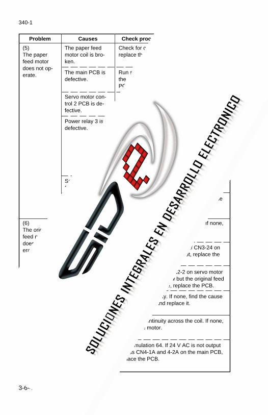
340-1
3-6-40
(5)The paperfeed motordoes not op-erate.
(6)The originalfeed motordoes not op-erate.
(7)The tonerfeed motordoes not op-erate.
The paper feedmotor coil is bro-ken.
The main PCB isdefective.
Servo motor con-trol 2 PCB is de-fective.
Power relay 3 isdefective.
Safety switch 1 or2 is defective.
The fuse on servomotor control 2PCB has blown.
The original feedmotor coil is bro-ken.
The main PCB isdefective.
Servo motor con-trol 2 PCB is de-fective.
The fuse on servomotor control 2PCB has blown.
The toner feedmotor coil is bro-ken.
The main PCB isdefective.
Check for continuity across the coil. If none,replace the motor.
Run simulation 11 and check if CN3-29 onthe main PCB goes low. If not, replace thePCB.
Run simulation 11. If CN2-8 on servo motorcontrol 2 PCB goes low but the paper feedmotor does not rotate, replace the PCB.
Check for continuity across the coil of powerrelay 3. If none, replace the relay.
Check if power relay 3 operates when CN6-20on the main PCB is set to high. If not, re-place the relay.
Check for continuity across power relay 3. Ifnone with the relay on, replace it.
Check for continuity across each safetyswitch. If none, replace it.
Check for continuity. If none, find the causeof fuse blowing and replace it.
Check for continuity across the coil. If none,replace the motor.
Run simulation 24 and check if CN3-24 onthe main PCB goes low. If not, replace thePCB.
Run simulation 24. If CN2-2 on servo motorcontrol 2 PCB goes low but the original feedmotor does not rotate, replace the PCB.
Check for continuity. If none, find the causeof fuse blowing and replace it.
Check for continuity across the coil. If none,replace the motor.
Run simulation 64. If 24 V AC is not outputacross CN4-1A and 4-2A on the main PCB,replace the PCB.
Problem Causes Check procedures/corrective measures

340-3
3-6-41
(8)The paperconveying fanmotor doesnot operate.
(9)The coolingfan motordoes not op-erate.
(10)The right orleft fixing unitfan motordoes not op-erate.
(11)LPH fan mo-tor 1 does notoperate.
(12)The upper rollwinding clutchdoes not op-erate.
The paper convey-ing fan motor isdefective.
The main PCB isdefective.
The cooling fanmotor is defective.
The main PCB isdefective.
The right or leftfixing unit fan mo-tor is defective.
The main PCB isdefective.
The coil of LPH fanmotor 1 has abreak.
LPH fan motor 1 isdefective.
The main PCB isdefective.
The upper rollwinding clutch coilis broken.
The connectorterminals of theupper roll windingclutch make poorcontact.
The main PCB isdefective.
Run simulation 18. If CN4-6A on the mainPCB goes low but the paper conveying fanmotor does not rotate, replace the motor.
Run simulation 18. If CN4-6A on the mainPCB does not go low, replace the PCB.
Run simulation 18. If CN6-3 on the mainPCB goes low but the cooling fan motordoes not rotate, replace the motor.
Run simulation 18. If CN6-3 on the mainPCB does not go low, replace the PCB.
Run simulation 18. If CN4-5A on the mainPCB goes low but the right or left fixing unitfan motor does not rotate, replace that mo-tor.
Run simulation 18. If CN4-5A on the mainPCB goes low replace the main PCB.
Check for continuity across the coil. If none,replace LPH fan motor 1.
Run simulation 18. If CN6-1 on the mainPCB goes low but LPH fan motor 1 does notrotate, replace the motor.
Run simulation 18. If CN6-1 on the mainPCB does not go low, replace the mainPCB.
Check for continuity across the coil. If none,replace the clutch.
Check for continuity across the terminals. Ifnone, replace them.
Run simulation 05. If CN4-9A on the mainPCB does not go low, replace the PCB.
Problem Causes Check procedures/corrective measures

340
3-6-42
(13)The middleroll windingclutch doesnot operate.
(14)The lower rollwindingclutch*1 doesnot operate.
(15)The upperfeed clutchdoes not op-erate.
(16)The middlefeed clutchdoes not op-erate.
The middle rollwinding clutch coilis broken.
The connectorterminals of themiddle roll windingclutch make poorcontact.
The main PCB isdefective.
The lower rollwinding clutch coilis broken.
The connectorterminals of thelower roll windingclutch make poorcontact.
The main PCB isdefective.
The upper feedclutch coil is bro-ken.
The connectorterminals of theupper feed clutchmake poor contact.
The main PCB isdefective.
The middle feedclutch coil is bro-ken.
The connectorterminals of themiddle feed clutchmake poor contact.
The main PCB isdefective.
Check for continuity across the coil. If none,replace the clutch.
Check for continuity across the terminals. Ifnone, replace them.
Run simulation 05. If CN6-11 on the mainPCB does not go low, replace the PCB.
Check for continuity across the coil. If none,replace the clutch.
Check for continuity across the terminals. Ifnone, replace them.
Run simulation 05. If CN6-13 on the mainPCB does not go low, replace the PCB.
Check for continuity across the coil. If none,replace the clutch.
Check for continuity across the terminals. Ifnone, replace them.
Run simulation 04. If CN4-8A on the mainPCB does not go low, replace the PCB.
Check for continuity across the coil. If none,replace the clutch.
Check for continuity across the terminals. Ifnone, replace them.
Run simulation 04. If CN6-10 on the mainPCB does not go low, replace the PCB.
Problem Causes Check procedures/corrective measures
*1 Optional.

340
3-6-43
(17)The lowerfeed clutch*1
does not op-erate.
(18)The roll paperconveyingclutch doesnot operate.
(19)The registra-tion clutchdoes not op-erate.
(20)The cutterclutch doesnot operate.
The lower feedclutch coil is bro-ken.
The connectorterminals of thelower feed clutchmake poor contact.
The main PCB isdefective.
The roll paper con-veying clutch coilis broken.
The connectorterminals of the rollpaper conveyingclutch make poorcontact.
The main PCB isdefective.
The registrationclutch coil is bro-ken.
The connectorterminals of theregistration clutchmake poor contact.
The main PCB isdefective.
The cutter clutchcoil is broken.
The connectorterminals of thecutter clutch makepoor contact.
The main PCB isdefective.
Check for continuity across the coil. If none,replace the clutch.
Check for continuity across the terminals. Ifnone, replace them.
Run simulation 04. If CN6-12 on the mainPCB does not go low, replace the PCB.
Check for continuity across the coil. If none,replace the clutch.
Check for continuity across the terminals. Ifnone, replace them.
Run simulation 06. If CN6-9 on the mainPCB does not go low, replace the PCB.
Check for continuity across the coil. If none,replace the clutch.
Check for continuity across the terminals. Ifnone, replace them.
Run simulation 06. If CN6-7 on the mainPCB does not go low, replace the PCB.
Check for continuity across the coil. If none,replace the clutch.
Check for continuity across the terminals. Ifnone, replace them.
Run simulation 06. If CN6-8 on the mainPCB does not go low, replace the PCB.
Problem Causes Check procedures/corrective measures
*1 Optional.

340
3-6-44
(21)The bypassregistrationclutch doesnot operate.
(22)The originalfeed clutchdoes not op-erate.
(23)The cleaningsolenoid doesnot operate.
(24)The separa-tion claw sole-noid does notoperate.
The bypass regis-tration clutch coil isbroken.
The connectorterminals of thebypass registrationclutch make poorcontact.
The main PCB isdefective.
The original feedclutch coil is bro-ken.
The connectorterminals of theoriginal feed clutchmake poor contact.
The main PCB isdefective.
The cleaning sole-noid coil is broken.
The connectorterminals of thecleaning solenoidmake poor contact.
The main PCB isdefective.
The separationclaw solenoid coilis broken.
The connectorterminals of theseparation clawsolenoid makepoor contact.
The main PCB isdefective.
Check for continuity across the coil. If none,replace the clutch.
Check for continuity across the terminals. Ifnone, replace them.
Run simulation 08. If CN6-14 on the mainPCB does not go low, replace the PCB.
Check for continuity across the coil. If none,replace the clutch.
Check for continuity across the terminals. Ifnone, replace them.
Run simulation 24. If CN4-7A on the mainPCB does not go low, replace the PCB.
Check for continuity across the coil. If none,replace the solenoid.
Check for continuity across the terminals. Ifnone, replace them.
Run simulation 45. If CN6-4 and CN6-5 onthe main PCB do not go low, replace thePCB.
Check for continuity across the coil. If none,replace the clutch.
Check for continuity across the terminals. Ifnone, replace them.
Run simulation 48. If CN6-6 on the mainPCB does not go low, replace the PCB.
Problem Causes Check procedures/corrective measures
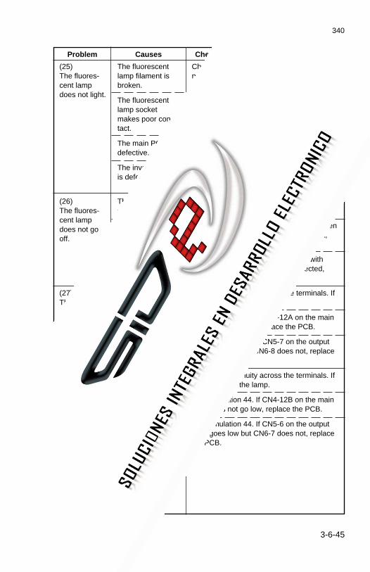
340
3-6-45
(25)The fluores-cent lampdoes not light.
(26)The fluores-cent lampdoes not gooff.
(27)The pre-charging lampdoes not light.
(28)The post-transfer lampdoes not light.
The fluorescentlamp filament isbroken.
The fluorescentlamp socketmakes poor con-tact.
The main PCB isdefective.
The inverter PCBis defective.
The main PCB isdefective.
The inverter PCBis defective.
The pre-charginglamp has a break.
The main PCB isdefective.
The output PCB isdefective.
The post-transferlamp has a break.
The main PCB isdefective.
The output PCB isdefective.
Check for continuity across the filament. Ifnone, replace the lamp.
Check for continuity across the right and leftlamp sockets.
Run simulation 110. If CN1-2 on the inverterPCB does not go low, replace the PCB.
Run simulation 110. If CN6-18 on the mainPCB goes low but the fluorescent lamp doesnot light, replace the inverter PCB.
Check if CN6-18 on the main PCB remainslow constantly. If so, replace the main PCB.
Check if the fluorescent lamp goes off whenCN1-2 on the inverter PCB is high. If not,replace the PCB.
If CN1-2 on the inverter PCB is low withCN6-18 on the main PCB disconnected,replace the inverter PCB.
Check for continuity across the terminals. Ifnone, replace the lamp.
Run simulation 44. If CN4-12A on the mainPCB fails to go low, replace the PCB.
Run simulation 44. If CN5-7 on the outputPCB goes low but CN6-8 does not, replacethe PCB.
Check for continuity across the terminals. Ifnone, replace the lamp.
Run simulation 44. If CN4-12B on the mainPCB does not go low, replace the PCB.
Run simulation 44. If CN5-6 on the outputPCB goes low but CN6-7 does not, replacethe PCB.
Problem Causes Check procedures/corrective measures

340
3-6-46
(29)Fixing heaterM or S doesnot turn on(C-630, C-631,C-640, C-641,C-650, C-660).
(30)Fixing heaterM or S fails toturn off (C-630,C-641, C-650,C-660).
Fixing heater M orS has a break.
Fixing unit thermalswitch 1 or 2 istripped.
Fixing unit thermis-tor 1 or 2 isshorted.
Solid state relay 1or 2 is defective.
The main PCB isdefective.
Solid state relay 1or 2 is defective.
The thermal sens-ing section of fixingunit thermistor 1 or2 is dirty.
Fixing unit thermis-tor 1 or 2 has abreak.
The main PCB isdefective.
Check for continuity across the terminals. Ifnone, replace the heater.
Check for continuity across the terminals. Ifnone, locate and remove the cause of theproblem and replace fixing unit thermalswitch 1 or 2.
Measure resistance. If it is 0 Ω, replace fix-ing unit thermistor 1 or 2.
Measure resistances across the terminals. Ifthey are other than ∞ Ω across 1 and 2 andcontinuity in one direction across 3 and 4,replace solid state relay 1 or 2.
Run simulation 47. If CN4-7B and CN4-8Bon the main PCB do not go low, replace thePCB.
Measure resistances across the terminals. Ifthey are other than ∞ Ω across 1 and 2 andcontinuity in one direction across 3 and 4,replace solid state relay 1 or 2.
Visually check and clean if necessary.
Measure the resistance. If it is ∞ Ω, replacethat thermistor.
Check if CN4-7B and CN4-8B on the mainPCB are low constantly. If so, replace thePCB.
Problem Causes Check procedures/corrective measures

340
3-6-47
(31)No maincharging.
(32)No transfercharging.
The main chargerwire is broken.
The main chargerhousing leaks.
The main high-voltage trans-former connectorsmake poor contact.
The main PCB isdefective.
The main high-voltage trans-former is defective.
The transfercharger wire isbroken.
The transfercharger housingleaks.
The ST high-volt-age transformerconnectors makepoor contact.
The main PCB isdefective.
The ST high-volt-age transformer isdefective.
See page 3-6-5.
See page 3-6-4.
Problem Causes Check procedures/corrective measures

340-1
3-6-48
(33)No separationcharging.
(34)No develop-ing bias.
(35)The job stop/roll cut keydoes not op-erate.
The separationcharger wire isbroken.
The ST high-volt-age transformerconnectors makepoor contact.
The main PCB isdefective.
The ST high-volt-age transformer isdefective.
The developingbias high-voltagetransformer con-nectors are notconnected cor-rectly or makepoor contacts.
The developingbias high-voltagetransformer is de-fective.
The main PCB isdefective.
The operation unitPCB is defective.
Visually check. Replace the wire if neces-sary.
Check if the connectors are securely con-nected. If not, remedy.
Check for continuity across the connectors.If none, replace them.
Run simulation 34 and, if CN4-2B on themain PCB does not go low, replace the mainPCB.
Run simulation 34. If separation charging isnot conducted with CN4-2B low, replace theST high-voltage transformer.
See page 3-6-9.
If CN1-8 on the operation unit PCB fails togo low when the job stop/roll cut key ispressed, replace the PCB.
Problem Causes Check procedures/corrective measures
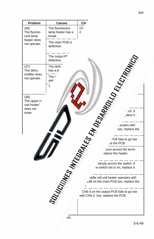
340
3-6-49
(36)The fluores-cent lampheater doesnot operate.
(37)The dehu-midifier doesnot operate.
(38)The upper rollunit heater*1
does not op-erate.
(39)The middleroll unit heater*1
does not op-erate.
The fluorescentlamp heater has abreak.
The main PCB isdefective.
The output PCB isdefective.
The dehumidifierhas a break.
The main PCB isdefective.
The output PCB isdefective.
The upper roll unitheater has abreak.
The upper roll unitheater switch isdefective.
The main PCB isdefective.
The output PCB isdefective.
The middle roll unitheater has abreak.
The middle roll unitheater switch isdefective.
The main PCB isdefective.
The output PCB isdefective.
Check the resistance across the terminals. Ifit is ∞ Ω, replace the heater.
If the fluorescent lamp heater operates withCN4-13B on the main PCB low, replace thePCB.
If CN6-6 on the output PCB fails to go lowwith CN5-5 low, replace the PCB.
Check the resistance across the terminals. Ifit is ∞ Ω, replace the heater.
If the dehumidifier operates with CN4-13Aon the main PCB low, replace the PCB.
If CN6-5 on the output PCB fails to go lowwith CN5-4 low, replace the PCB.
Measure the resistance across the termi-nals. If it is ∞ Ω, replace the heater.
Check for continuity across the switch. Ifnone with the switch set to on, replace it.
If the upper roll unit heater operates withCN4-14A on the main PCB low, replace thePCB.
If CN6-4 on the output PCB fails to go lowwith CN5-3 low, replace the PCB.
Measure the resistance across the termi-nals. If it is ∞ Ω, replace the heater.
Check for continuity across the switch. Ifnone with the switch set to on, replace it.
If the middle roll unit heater operates withCN4-14B on the main PCB low, replace thePCB.
If CN6-3 on the output PCB fails to go lowwith CN5-2 low, replace the PCB.
Problem Causes Check procedures/corrective measures
*1 Optional for 220 – 240 V models.

340-3
3-6-50
(40)The lowerroller unitheater*1 doesnot operate.
(41)LPH fan mo-tor 2 does notoperate.
The lower roll unitheater has abreak.
The lower roll unitheater switch isdefective.
The main PCB isdefective.
The output PCB isdefective.
The coil of LPH fanmotor 2 has abreak.
LPH fan motor 2 isdefective.
The main PCB isdefective.
Measure the resistance across the termi-nals. If it is ∞ Ω, replace the heater.
Check for continuity across the switch. Ifnone with the switch set to on, replace it.
If the lower roll unit heater operates withCN4-15A on the main PCB low, replace thePCB.
If CN6-2 on the output PCB fails to go lowwith CN5-1 low, replace the PCB.
Check for continuity across the coil. If none,replace LPH fan motor 2.
Run simulation 18. If CN6-15 on the mainPCB goes low but LPH fan motor 2 does notrotate, replace the motor.
Run simulation 18. If CN6-15 on the mainPCB does not go low, replace the mainPCB.
Problem Causes Check procedures/corrective measures
*1 Optional.
340-1
3-6-51
If they are, clean with iso-propyl alcohol.
Replace if necessary.
If they are, clean with iso-propyl alcohol.
Replace if necessary.
If they are, clean with iso-propyl alcohol.
Replace if necessary.
If it is, clean with isopropylalcohol.
Replace if necessary.
If CN3-14 on the mainPCB does not change lev-els when the bypass regis-tration switch is turned onand off, replace the switch.
If it is, replace the switch.
(1)No primarypaper feed.
Check if the surface of the roll paperfeed upper roller of the 1st roll unitand that of roll paper feed lowerroller A are dirty with paper dust.
Check if the roll paper feed upperroller of the 1st roll unit and roll pa-per feed lower roller A are deformedor worn.
Check if the surface of the roll paperfeed upper roller of the 2nd roll unitand that of roll paper feed rear rollerB are dirty with paper dust.
Check if the roll paper feed upperroller of the 2nd roll unit and roll pa-per feed rear roller B are deformedor worn.
Check if the surface of the roll paperfeed upper roller of the 3rd roll unit(optional) and that of roll paper feedrear roller C are dirty with paperdust.
Check if the roll paper feed upperroller of the 3rd roll unit (optional)and paper feed rear roller C are de-formed or worn.
Check if the surface of roll paperconveying rear roller A is dirty withpaper dust.
Check if roll paper conveying rearroller A is deformed or worn.
Check if the bypass registrationswitch operates correctly.
Check if the bypass registrationswitch actuator is broken.
3-6-5 Mechanical problems
Problem Causes/check procedures Corrective measures

340
3-6-52
(1)No primarypaper feed.(cont.)
(2)No secondarypaper feed.
(3)No originalconveying.
Check if the surface of the bypasspaper feed roller is dirty with paperdust.
Check if the bypass paper feed rolleris deformed or worn.
Check if the bypass registrationclutch, upper feed clutch, middlefeed clutch, lower feed clutch (op-tional), and roll paper conveyingclutch are installed correctly.
Check if the bypass registrationclutch, upper feed clutch, middlefeed clutch, lower feed clutch (op-tional) or roll paper conveying clutchoperates correctly.
Check if paper feed section drivebelts 1 and 2 are installed correctly.
Check if the surfaces of the regis-tration roller and registration pulleyare dirty with paper dust.
Check if the surfaces of the bypassregistration roller, bypass pulley andpre-transfer roller are dirty with pa-per dust.
Check if the registration clutch orbypass registration clutch is installedcorrectly.
Check if the registration clutch orbypass registration clutch operatescorrectly.
Check if the surfaces of the frontupper, middle upper, rear upper,front lower and rear lower originalrollers are dirty with paper dust.
Check if the front upper or rear up-per original roller is deformed orworn.
If it is, clean with isopropylalcohol.
If it is, replace the roller.
If not, reinstall.
If not, replace the compo-nent.
If not, reinstall (see pages3-3-60 and 61).
If they are, clean with iso-propyl alcohol.
If they are, clean with iso-propyl alcohol.
If not, reinstall.
If not, replace the clutch.
If they are, clean with iso-propyl alcohol.
If it is, replace.
Problem Causes/check procedures Corrective measures

340
3-6-53
Problem Causes/check procedures Corrective measures
(3)No originalconveying.(cont.)
(4)Original jam.
(5)Paper jam.
Check if the original leading edgedetection switch operates correctly.
Check if the actuator of the originalleading edge detection switch is bro-ken.
Check if the original feed clutch isinstalled correctly.
Check if the original feed clutch op-erates correctly.
Check if original drive belts 1 and 2are installed correctly.
Check if the original holding sectionis installed correctly.
Check if a guide plate or other com-ponent along the original conveyingpath is deformed.
Check the paper.
Check if the separation charger wireon the transfer charger assembly isbroken.
Check if the paper conveying fanmotor rotates correctly.
Check if a guide plate or other com-ponent along the paper conveyingpath is deformed.
Check if the press roller or the sepa-ration claws are extremely dirty.
Check if the press roller or a separa-tion claw is deformed.
Check if the oil roller is extremelydirty.
If CN3-12 on the mainPCB does not change lev-els when the original lead-ing edge detection switchis turned on and off, re-place the switch.
If it is, replace the switch.
If not, reinstall.
If not, replace the clutch.
If not, reinstall.
If not, reinstall.
If it is, correct or replace.
If the paper is extremelycurled or has other prob-lems, replace.
If it is, replace (see page3-3-37).
If not, replace the motor.
If it is, correct or replace.
If so, clean.
If so, replace (see page3-3-52).
If it is, replace (see page3-3-53).

340
3-6-54
Problem Causes/check procedures Corrective measures
(6)Toner fallsonto the pa-per conveyingsection.
(7)Abnormalnoise.
Check if the developing section isextremely dirty.
Check if the lower cleaning blade isdeformed.
Check if all the rollers and gearsrotate smoothly.
Check if all the drive belts aretensioned correctly.
If it is, clean the develop-ing section and aroundthat area.
If it is, replace.
If there is a problem,grease the bearings andgears.
If not, adjust (see pages3-3-60, 61, 62 and 63).

1-1-33
340
CONTENTS
3-7 Appendixes
Timing chart No. 1 ......................................................................................... 3-7-1Timing chart No. 2 ......................................................................................... 3-7-2Timing chart No. 3 ......................................................................................... 3-7-3Timing chart No. 4 ......................................................................................... 3-7-4Timing chart No. 5 ......................................................................................... 3-7-5Main PCB 1/44 .............................................................................................. 3-7-6Main PCB 2/44 .............................................................................................. 3-7-7Main PCB 3/44 .............................................................................................. 3-7-8Main PCB 4/44 .............................................................................................. 3-7-9Main PCB 5/44 ............................................................................................ 3-7-10Main PCB 6/44 ............................................................................................ 3-7-11Main PCB 7/44 ............................................................................................ 3-7-12Main PCB 8/44 ............................................................................................ 3-7-13Main PCB 9/44 ............................................................................................ 3-7-14Main PCB 10/44 .......................................................................................... 3-7-15Main PCB 11/44 .......................................................................................... 3-7-16Main PCB 12/44 .......................................................................................... 3-7-17Main PCB 13/44 .......................................................................................... 3-7-18Main PCB 14/44 .......................................................................................... 3-7-19Main PCB 15/44 .......................................................................................... 3-7-20Main PCB 16/44 .......................................................................................... 3-7-21Main PCB 17/44 .......................................................................................... 3-7-22Main PCB 18/44 .......................................................................................... 3-7-23Main PCB 19/44 .......................................................................................... 3-7-24Main PCB 20/44 .......................................................................................... 3-7-25Main PCB 21/44 .......................................................................................... 3-7-26Main PCB 22/44 .......................................................................................... 3-7-27Main PCB 23/44 .......................................................................................... 3-7-28Main PCB 24/44 .......................................................................................... 3-7-29Main PCB 25/44 .......................................................................................... 3-7-30Main PCB 26/44 .......................................................................................... 3-7-31Main PCB 27/44 .......................................................................................... 3-7-32Main PCB 28/44 .......................................................................................... 3-7-33Main PCB 29/44 .......................................................................................... 3-7-34Main PCB 30/44 .......................................................................................... 3-7-35Main PCB 31/44 .......................................................................................... 3-7-36Main PCB 32/44 .......................................................................................... 3-7-37Main PCB 33/44 .......................................................................................... 3-7-38Main PCB 34/44 .......................................................................................... 3-7-39Main PCB 35/44 .......................................................................................... 3-7-40Main PCB 36/44 .......................................................................................... 3-7-41Main PCB 37/44 .......................................................................................... 3-7-42Main PCB 38/44 .......................................................................................... 3-7-43Main PCB 39/44 .......................................................................................... 3-7-44

1-1-34
340
Main PCB 40/44 .......................................................................................... 3-7-45Main PCB 41/44 .......................................................................................... 3-7-46Main PCB 42/44 .......................................................................................... 3-7-47Main PCB 43/44 .......................................................................................... 3-7-48Main PCB 44/44 .......................................................................................... 3-7-49ISU PCB 1/10 .............................................................................................. 3-7-50ISU PCB 2/10 .............................................................................................. 3-7-51ISU PCB 3/10 .............................................................................................. 3-7-52ISU PCB 4/10 .............................................................................................. 3-7-53ISU PCB 5/10 .............................................................................................. 3-7-54ISU PCB 6/10 .............................................................................................. 3-7-55ISU PCB 7/10 .............................................................................................. 3-7-56ISU PCB 8/10 .............................................................................................. 3-7-57ISU PCB 9/10 .............................................................................................. 3-7-58ISU PCB 10/10 ............................................................................................ 3-7-59Backup PCB ................................................................................................ 3-7-60Servo motor control 1 PCB 1/3 ................................................................... 3-7-61Servo motor control 1 PCB 2/3 ................................................................... 3-7-62Servo motor control 1 PCB 3/3 ................................................................... 3-7-63Output PCB ................................................................................................. 3-7-64LPH power supply PCB ............................................................................... 3-7-65Servo motor control 2 PCB ......................................................................... 3-7-66Operation unit PCB ..................................................................................... 3-7-67Power source PCB 1/2 ................................................................................ 3-7-68Power source PCB 2/2 ................................................................................ 3-7-69Detachable unit wiring diagram ................................................................... 3-7-70General connection diagram ....................................................................... 3-7-71General wiring diagram ............................................................................... 3-7-72

AA A
A
AA A
A
E
E E
E
E
E E
E
EA
EA
Xi 3648/8020 (MCA/MCE)
3-7-1
340
Timing chart No. 1 From the main switch being turned on to copier stabilization
DB CHG (+) CN4-4B
DB REM CN4-3B
FDM CN7-6
CSOL 1 CN6-5
CSOL 2 CN6-4
FL CN6-18
SC REM CN4-2B
MC REM CN6-17
FFM-R FFM-L
CN4-5A CN4-5B
PCFM CFM
CN4-6A CN6-3
LPHFM1 LPHFM2
CN6-1 CN6-2
DM DRM PCHL REM RTL REM
CN7-6 CN7-1
CN4-12A CN4-12B
MS
W: O
n
Prim
ary
fixin
g
stab
iliza
tion*
1
Sec
onda
ry fi
st
abili
zatio
n*2
100 ms
200 ms1 s
1 s
3.534 s
*1 TETTH ≤ 15°C/59°F: 145°C/293°F 15°C/59°F < TETTH < 30°C/86°F: 165°C/329°F 30°C/86°F ≤ TETTH: 165°C/329°F
*2 TETTH ≤ 15°C/59°F: 165°C/329°F 15°C/59°F < TETTH < 30°C/86°F: 155°C/311°F 30°C/86°F ≤ TETTH: 155°C/311°F
100 ms
300 ms
100 ms
300 ms
200 ms
10 min
3.543 s × 2
1 s 1 s 1 s 1 s
TETTH: external temperature thermistor temperature

AA A A
A
AA A A
A
E
E E E
E
E
E E E
E
Xi 3648/8020 (MCA/MCE)
3-7-2
340
Timing chart No. 2 Bypass paper feed, with the paper inserted before the original
ESW CN3-16
OLDSW CN3-12
OTDSW CN3-13
BYPRSW CN3-14
BYPTIMSW CN3-34
PCSW CN3-15
DB CHG(+) CN4-4B
DB REM CN4-3B
FDM CN7-6
CSOL 1 CN6-5
CSOL 2 CN6-4
TC REM CN4-1B
SC REM CN4-2B
OFM CN3-23 – 25
OFCL CN4-7A
FL CN6-18
FFM-R CN4-5A FFM-L CN4-5B
PCFM CN4-6A CFFM CN6-3
LPHFM1 CN6-1 LPHFM2 CN6-2
MC REM CN6-17
BPRCL CN6-14
SSOL CN6-6
CCL CN6-8
PFM CN3-29
OSYNC signalPSYNC signal
DM CN7-2 DRM CN7-1 PCHL REM CN4-12A RTL REM CN4-12B
1 s
100 ms1 s
1 s
100 ms
300 ms
300 ms
1704 ms
540 ms
3.534 s
1.75 s
640 ms
1 s
Half speed
Half speed
Stop
Half speed
Half speedFull speed
Full speed
Full speedStop
944 ms
200 ms
450 ms
600 ms
1325 ms
3.543 s × 2
1680 ms
4.6 s
78P*
100 ms
300 ms 200 ms
1 s 1 s 1 s 1 s
10 min
5.2 s
450 ms
BY
PR
SW
: On
Inpu
t
BY
PR
TIM
SW
: O
nO
LDS
W: O
n
OT
DS
W: O
n
PC
SW
: On
ES
W: O
n
BY
PR
SW
: Off
BY
PT
IMS
W:
Off
OLD
SW
: Off
OT
DS
W: O
ff
PC
SW
: Off
ES
W: O
ff
Shading correction start * Varies depending on the setting in simulation 56.
Out
put

AA A
A
AA A
A
E
E E
E
E
E E
E
EA
EA
Xi 3648/8020 (MCA/MCE)
3-7-3
340
Timing chart No. 3 Bypass paper feed, with the original inserted before the paper
BY
PR
SW
: On
BY
PT
IMS
W: O
n
OLD
SW
: On
OT
DS
W: O
n
1704 ms
540 ms
Half speed
Half speedFull speed
Full speed
Full speedStop
Half speed
Half speed
Stop
944 ms
200 ms
450 ms
600 ms
1325 ms
3.543 s × 2
1680 ms
4.6 s
78P*
100 ms
300 ms 200 ms
1 s 1 s 1 s 1 s
10 min
5.2 s
450 ms
PC
SW
: On
ES
W: O
n
BY
PR
SW
: Off
BY
PT
IMS
W: O
ff
OLD
SW
: Off
OT
DS
W: O
ff
PC
SW
: Off
ES
W: O
ffShading correction start
* Varies depending on the setting in simulation 56.
ESW CN3-16
OLDSW CN3-12
OTDSW CN3-13
BYPRSW CN3-14
BYPTIMSW CN3-34
PCSW CN3-15
DB CHG(+) CN4-4B
DB REM CN4-3B
FDM CN7-6
CSOL 1 CN6-5
CSOL 2 CN6-4
TC REM CN4-1B
SC REM CN4-2B
OFM CN3-23 – 25
OFCL CN4-7A
FL CN6-18
FFM-R CN4-5A FFM-L CN4-5B
PCFM CN4-6A CFM CN6-3
LPHFM1 CN6-1 LPHFM2 CN6-2
MC REM CN6-17
BPRCL CN6-14
SSOL CN6-6
CCL CN6-8PFM CN3-29OSYNC signalPSYNC signal
DM CN7-2 DRM CN7-1 PCHL REM CN4-12A RTL REM CN4-12B
Inpu
tO
utpu
t
640 ms
1.75 s 750 ms
3.534 s
200 ms
1 s
1 s
100 ms 300 ms
100 ms750 ms

AA A A
A
AA A A
A
E
E E E
E
E
E E E
E
Xi 3648/8020 (MCA/MCE)
3-7-4
340
Timing chart No. 4 Roll unit paper feed, single copy
1 s
1 s
1 s
100 ms
100 ms 300 ms
200 ms
640 ms
3.534 s
100 ms
200 ms300 ms
10 min
1 s 1 s 1 s 1 s
1680 ms
5.2 s
1704 ms
574 ms*2 200 ms
4.6 s
3.534 s × 2
450 ms
600 ms
944 ms 78 P*1
1325 ms
OLD
SW
: On
OT
DS
W: O
n
RS
W: O
n
PC
SW
: On
ES
W: O
n
OLD
SW
: Off
OT
DS
W: O
ff
RS
W: O
ff
PC
SW
: Off
ES
W: O
ff
ESW
OLDSW
OTDSW
PCSW
RSW
DB CHG(+)
DB REM
FDM
CSOL 1
CSOL 2
TC REM
SC REM
PFM
FCL-UFCL-M
RPCCL
RCLDMDRMPCHL REMRTL REMMC REM
SSOL
CCL
OSYNC signalPSYNC signal
OFM
OFCL
FL
FFM-RFFM-LPCFMCFMLPHFM1LPHFM2
CN3-16
CN3-12
CN3-13
CN3-15
CN3-11
CN4-4B
CN4-3B
CN7-6
CN6-5
CN6-4
CN4-1B
CN4-2B
CN3-29
CN4-8ACN6-10
CN6-9
CN6-7CN7-6CN7-1
CN4-12ACN4-12B
CN6-17
CN6-6
CN6-8
CN6-18
CN3-23 – 25
CN4-7A
CN4-5ACN4-5BCN6-4ACN6-3A
CN6-1CN6-2
Out
put
Inpu
t
Half speed
Stop
Shading correction start
Half speed
Half speed
StopFull speed
Full speed
Full speed
Half speed
*1 Varies depending on the setting in simulation 56. *2 Varies depending on the setting in simulation 57.

AA A
A
AA A
A
E
E E
E
E
E E
E
EA
EA
Xi 3648/8020 (MCA/MCE)
3-7-5
340
Timing chart No. 5 Roll unit paper feed, continuous two copies
1 s
1704 ms
574 ms*2
944 ms
450 ms
500 ms48 ms
1325 ms
600 ms
78 P*1
4.6 s
200 ms3.534 s × 2
1680 ms
5.25 s1 s 1 s 1 s 1 s
10 min
200 ms
300 ms
100 ms
200 ms
500 ms
1 s
1 s
1 s
100 ms
300 ms
1704 ms 1680 ms
200 ms
100 ms
574 ms*2
3.534 s
944 ms
450 ms
640 ms
78 P*1
200 ms
600 ms
OLD
SW
: On
OT
DS
W: O
n
RS
W: O
n
PC
SW
: On
ES
W: O
n
OLD
SW
: Off
OLD
SW
: On
OT
DS
W: O
ff
PC
SW
: On
PC
SW
: Off
ES
W: O
n
ES
W: O
ff
OLD
SW
: Off
OT
DS
W: O
ff
OT
DS
W: O
n
OT
DS
W: O
n
RS
W: O
ff
RS
W: O
ff
OT
DS
W: O
ffR
SW
: Off
PC
SW
: Off
ES
W: O
ff
ESW
OLDSW
OTDSW
PCSW
RSW
DB CHG(+)
DB REM
FDM
CSOL 1
CSOL 2
TC REM
SC REM
PFM
FCL-UFCL-M
RPCCL
RCLDMDRMPCHL REMRTL REM
MC REM
SSOL
CCL
OSYNC signalPSYNC signal
OFM
OFCL
FLFFM-RFFM-L
PCFMCFM
LPHFM1LPHFM2
CN3-16
CN3-12
CN3-13
CN3-15
CN3-11
CN4-4B
CN4-3B
CN7-6
CN6-5
CN6-4
CN4-1B
CN4-2B
CN3-29
CN4-8ACN6-10
CN6-9
CN6-7CN7-6CN7-1
CN4-12ACN4-12B
CN6-17
CN6-6
CN6-8
CN6-18
CN3-23 – 25
CN4-7A
CN4-5ACN4-5B
CN6-4ACN6-3A
CN6-1CN6-2
Stop
Out
put
Inpu
t
*1 Varies depending on the setting in simulation 56. *2 Varies depending on the setting in simulation 57.Shading correction start
(+)
(–)
Half speed
Half speed
Full speed
Full speed
Full speed
Stop
Half speed
Half speed
Stop

AA A A
A
AA A A
A
E
E E E
E
E
E E E
E
A B C D E F G H I J
A B C D E F G H I J
1
2
3
4
5
6
7
8
1
2
3
4
5
6
7
8
PointSource Ai3030/Vi300(MCA/MCE) S/M
3-7-10
185
IPU PCB 1/20
+SVD0
-SVD0
-SVD1
+SVD1
-SVD2
+SVD2
-SVD3
+SVD3
-SVD4
+SVD4
-SVD5
+SVD5
-SVD6
+SVD6
-SVD7
+SVD7
iISUD(7:0)
S001 IPCK6 (013B10) (014B10) (020F11)
S002 IPCK5 (008J04) (009B02) (020F11)
S003 IPCK4 (005G16) (006E02) (007J01) (020E11)
S004 IPCK3 (003E02) (004C02) (020E11)
S005 FG1 (001D10) (001H10) (001I01)
FG1(001K09)
(002C01)
CON26A
CON626
CON26A
CON613
CON26A
CON625
CON26A
CON612
CON26A
CON624
CON26A
CON611
CON26A
CON623
CON26A
CON610
CON26A
CON622
CON26A
CON69
CON26A
CON621
CON26A
CON68
CON26A
CON620
CON26A
CON67
CON26A
CON619
CON26A
CON66
CON26A
CON618
CON26A
CON6 NF10C24 NF27
VPL5
NF28
VPL5
GPL5
GPL5
GPL5
IC3
GPL5
16
32 OUT A
OUT B
OUT C
OUT D
END
VCC
1141567
109
4
8
13
5
11
12
GND
EN
IND8IND1INC0INC1INB0INB1INA0INA1
GPL5
GPL5
RA4
IC4
GPL5
16
32 OUT A
OUT B
OUT C
OUT D
END
VCC
1141567
109
4
8
13
5
11
12
GND
EN
IND8IND1INC0INC1INB0INB1INA0INA1
C23R31
C22
C21R29
R56
R54
R55
R53
R49
R47
R48 5
4
0
1
1 2 3 4 5 6 7
2 3 4 5 6 7 8 9
7
6
1
0
3
2
R46
NF9
NF12
NF11
NF13
NF14
NF15
NF16
NF18
NF17
NF20
NF19
NF21
NF22
NF23
NF24 R28
R45
R50
R51
R30
R52
R57
R58
5
+SPGTCON26A
CON6 NF6
C26 NF25
NF26
TP4
TP5
VPL5
GPL5
GPL5
C25R32
R41
NF5
NF7
NF8 R40
3
-SPGTCON26A
CON616
+ADCKCON26A
CON64
-ADCKCON26A
CON617
FG1(001K09)
FG1
FG1
X1
(001K09)
GPL5
IC2
GPL5
GPL5
GPL5
16
32 OUT A
OUT B
OUT C
OUT D
END
VCC
1141567
109
4
8
13
5
11
12
GND
IC1
5 _DO
C27
6 DO7 _RI8
4321RI
GNDDI
RDVCC
EN
IND8IND1INC0INC1INB0INB1INA0INA1
iADCK (002D01)
TP3iOVSYNC (006B02)
TP11NF79
NF78
NF92
NF93
NF95
NF96
NF97
NF82
iPCK1 (002F01)(020E11)iPCK2 (002J01)(020E11)iPCK3
S004
iPCK5S002
iPCK6S001
_iPCK7(017H15)(020F11)
_iPCK8 (013B10)
iPCK4S003
_iOHSYNC (006E15)
iSPGT (002D01)
VPL5
VPL5
NF1
R33
+OVSYNCCON26A
CON61
NF2
R32
R31
-OVSYNCCON26A
CON614
NF3+OHSYNC
CON26A
CON62
NF4-OHSYNC
CON26A
CON615
GPL5
GPL5GPL5GPL5GPL5GPL5
1 NC
GND
VCC48MHz
OUT4
8C34
C29
C28
NF98
NF81
NF80
C35
5
GPL5 GMI5
VPL5 VPL5 VPL5
IC18
1213101114345
VCC1VCC2_PRE>CP_CLRGND1GND2GND3
O1O2O3O4O5O6
_O7_O8
1516126789
R17
R14
R65
R42

AA A
A
AA A
A
E
E E
E
E
E E
E
EA
EA
A B C D E F G H I J
A B C D E F G H I J
1
2
3
4
5
6
7
8
1
2
3
4
5
6
7
8
185
3-7-11
PointSource Ai3030/Vi300(MCA/MCE) S/M
IPU PCB 2/20
GPL5IC16
GPL5
GPL5
C31
C32VPL5
NF76
R59GPL5
C50
C51VPL5
NF90
R72GPL5
C66
C67VPL5
NF102
R83GPL5
C78
C79VPL5
NF107
R92
GPL5
C121
C122VPL5
NF128
R117GPL5
C103
C104VPL5
NF119
R113GPL5
C93
C94VPL5
NF113
R109
0 1 2 3 4 5 6 7
8 7 6 5 8 7 6 5
24 23 22 21 16 15 14 13
DI0 DI1 DI2 DI3 DI4 DI5 DI6 DI7 WE0 WCK RSTW0 GND
DO0 DO1 DO2 DO3 DO4 DO5 DO6 DO7 RE0 RCK
RSTR0 VCC
1 2 3 4 9 10 11 12
1 2 3 4 1 2 3 4
0 1 2 3 4 5 6 7
iSPGT(001C16)
iADCK(001C16)
iISUD(7:0)(001G08)
iMREOUTA(003G15)
iIDOUTA(7:0)(003H15)
RA34
2 3 4 5 6 7 8 9
0 1 2 3 4 5 6 7
GPL5
TP18
S001 IID12 (003F15) (005B01) (008J04)
iPCK2(001H15)
(001H15)
(007J08)
(001H15)
(007J08)
(001H15)
(007J08)iPCK1
(001H15)
iMREB1(007J08)
20 17 19 7
5 8 6 18
GPL5IC19
GPL5
0 1 2 3 4 5 6 7
8 7 6 5 8 7 6 5
24 23 22 21 16 15 14 13
DI0 DI1 DI2 DI3 DI4 DI5 DI6 DI7 WE0 WCK RSTW0 GND
DO0 DO1 DO2 DO3 DO4 DO5 DO6 DO7 RE0 RCK
RSTR0 VCC
1 2 3 4 9 10 11 12
1 2 3 4 1 2 3 4
0 1 2 3 4 5 6 7
20 17 19 7
5 8 6 18
GPL5IC27
GPL5
0 1 2 3 4 5 6 7
8 7 6 5 8 7 6 5
24 23 22 21 16 15 14 13
DI0 DI1 DI2 DI3 DI4 DI5 DI6 DI7 WE0 WCK RSTW0 GND
DO0 DO1 DO2 DO3 DO4 DO5 DO6 DO7 RE0 RCK
RSTR0 VCC
1 2 3 4 9 10 11 12
1 2 3 4 1 2 3 4
0 1 2 3 4 5 6 7
20 17 19 7
5 8 6 18
GPL5IC35
GPL5
0 1 2 3 4 5 6 7
8 7 6 5 8 7 6 5
24 23 22 21 16 15 14 13
DI0 DI1 DI2 DI3 DI4 DI5 DI6 DI7 WE0 WCK RSTW0 GND
DO0 DO1 DO2 DO3 DO4 DO5 DO6 DO7 RE0 RCK
RSTR0 VCC
1 2 3 4 9 10 11 12
1 2 3 4 1 2 3 4
0 1 2 3 4 5 6 7
20 17 19 7
5 8 6 18
GPL5IC54
GPL5
0 1 2 3 4 5 6 7
8 7 6 5 8 7 6 5
24 23 22 21 16 15 14 13
DI0 DI1 DI2 DI3 DI4 DI5 DI6 DI7 WE0 WCK RSTW0 GND
DO0 DO1 DO2 DO3 DO4 DO5 DO6 DO7 RE0 RCK
RSTR0 VCC
1 2 3 4 9 10 11 12
1 2 3 4 1 2 3 4
0 1 2 3 4 5 6 7
20 17 19 7
5 8 6 18
GPL5IC50
GPL5
0 1 2 3 4 5 6 7
8 7 6 5 8 7 6 5
24 23 22 21 16 15 14 13
DI0 DI1 DI2 DI3 DI4 DI5 DI6 DI7 WE0 WCK RSTW0 GND
DO0 DO1 DO2 DO3 DO4 DO5 DO6 DO7 RE0 RCK
RSTR0 VCC
1 2 3 4 9 10 11 12
1 2 3 4 1 2 3 4
0 1 2 3 4 5 6 7
20 17 19 7
5 8 6 18
GPL5IC44
GPL5
RA97 RA98
0 1 2 3 4 5 6 7
8 7 6 5 8 7 6 5
24 23 22 21 16 15 14 13
DI0 DI1 DI2 DI3 DI4 DI5 DI6 DI7 WE0 WCK RSTW0 GND
DO0 DO1 DO2 DO3 DO4 DO5 DO6 DO7 RE0 RCK
RSTR0 VCC
1 2 3 4 9 10 11 12
1 2 3 4 1 2 3 4
0 1 2 3 4 5 6 7
20 17 19 7
5 8 6 18
RA112 RA113
RA129 RA130
RA77 RA78
RA58 RA59
RA38 RA39
RA18 RA19
iID10(7:0)(003J15)
iID14(7:0)(005B16)
iID15(7:0)(005B16)
iID16(7:0)(005C16)
iID11(7:0)(003G15)
iID12(7:0)S001
iID13(7:0)(003D15) (005B16)

AA A A
A
AA A A
A
E
E E E
E
E
E E E
E
A B C D E F G H I J
A B C D E F G H I J
1
2
3
4
5
6
7
8
1
2
3
4
5
6
7
8
PointSource Ai3030/Vi300(MCA/MCE) S/M
3-7-12
185
IPU PCB 3/20
_iACPWRES(004C02)
_iACPRRES(004D02)
iACPRD1(7:0)(004E12)
iACPWD1(7:0) ACPWD1_0(7:0) ACPWD0_0(7:0)
iACPRD0(7:0)
RA50
RA55
RA60
RA61
(004E02)
iACPWD2(7:0)(004I02)
iACPRD2(7:0)(004I12)
iPCK3(001H15)
iOVST(006E15)
iPVST(006E15)
_iOHSYNC(006E15)
iMREAD(006D02)
iMREACP(005F16)
iCHAR(005E16)
iSCREEN(005E16)
iACPD(7:0)(006G02)
0 1 2 3
1 2 3 4
8 7 6 5
0 1 2 3
4 5 6 7
1 2 3 4
8 7 6 5
0 1 2 3
1 2 3 4
8 7 6 5
157 158 159 160 161 162 163 164 165 166 167 168 169 170 171 172 173 174 175 176 177 178 179 180 181 182 183 184 185 186 187 188 189 190 191 192 193 194 195 196 197 198 199 200 201 202 203 204 205 206 207 208
1 2 3 4 5 6 7 8 9 10
11
12
13
14
15
16
17
18
19
20
21
22
23
24
25
26
27
28
29
30
31
32
33
34
35
36
37
38
39
40
41
42
43
44
45
46
47
48
49
50
51
52
156
155
154
153
152
151
150
149
148
147
146
145
144
143
142
141
140
139
138
137
136
135
134
133
132
131
130
129
128
127
126
125
124
123
122
121
120
119
118
117
116
115
114
113
112
111
110
109
108
107
106
105
VDD13 FF2DW0 FF2DW1 FF2DW2 FF2DW3 GND30 FF2DW4 FF2DW5 FF2DW6 FF2DW7 GND31 TEST14 TEST15 VDD14 FF2DR0 FF2DR1 FF2DR2 FF2DR3 GND32 FF2DR4 FF2DR5 FF2DR6 FF2DR7 GND33 PCK GND34 VDD15 TEST16 TEST17 OVST PVST OHSYNC_ TEST18 TEST19 GND35 AOUT0 AOUT1 AOUT2 AOUT3 GND36 VDD16 AOUT4 AOUT5 AOUT6 AOUT7 GND37 VDD17 MREA0 MREACP CHAR SCREEN VDD18
GN
D1
GN
D2
RE
SE
T_
GN
D3
A0
A1
A2
A3
A4
AC
PC
S_
IDW
R_
IDR
D_
VD
D1
GN
D4
D0
D1
GN
D5
D2
D3
VD
D2
D4
D5
GN
D6
D6
D7
GN
D7
VD
D3
RE
GIN
0 R
EG
IN1
RE
GIN
2 R
EG
IN3
GN
D8
RE
GIN
4 R
EG
IN5
RE
GIN
6 R
EG
IN7
VD
D4
TE
ST
0 T
ES
T1
TE
ST
2 T
ES
T3
IDE
XT
0 ID
EX
T1
IDE
XT
2 ID
EX
T3
GN
D9
IDE
XT
4 ID
EX
T5
IDE
XT
6 ID
EX
T7
GN
D10
G
ND
11
104 103 102 101 100 99 98 97 96 95 94 93 92 91 90 89 88 87 86 85 84 83 82 81 80 79 78 77 76 75 74 73 72 71 70 69 68 67 66 65 64 63 62 61 60 59 58 57 56 55 54 53
VDD9 IDIND7 IDIND6 IDIND5 IDIND4 GND18 IDIND3 IDIND2 IDIND1 IDIND0
VDD8 TEST9 TEST8
MRE GND17 IDINC7 IDINC6 IDINC5 IDINC4 GND16 IDINC3IDINC2 IDINC1 IDINC0 TEST7 GND15
VDD7 TEST6 IDINB7 IDINB6 IDINB5 IDINB4 GND14 IDINB3IDINB2 IDINB1 IDINB0 VDD6 WRS_ TEST5 TEST4 GND13
IDOUTA7 IDOUTA6 IDOUTA5 IDOUTA4
GND12 IDOUTA3IDOUTA2 IDOUTA1 IDOUTA0
VDD5
GN
D29
G
ND
28
FF
1DR
7 F
F1D
R6
FF
1DR
5 F
F1D
R4
GN
D27
F
F1D
R3
FF
1DR
2 F
F1D
R1
FF
1DR
0 V
DD
12
TE
ST
13
TE
ST
12
GN
D26
F
F1D
W7
FF
1DW
6 F
F1D
W5
FF
1DW
4 G
ND
25
FF
1DW
3 F
F1D
W2
FF
1DW
1 F
F1D
W0
FF
RR
S_
GN
D24
V
DD
11
FF
WR
S_
FF
OD
R7
FF
OD
R6
FF
OD
R5
FF
OD
R4
GN
D23
F
FO
DR
3 F
FO
DR
2 F
FO
DR
1 F
FO
DR
0 V
DD
10
TE
ST
11
TE
ST
10
GN
D22
F
FO
DW
7 F
FO
DW
6 F
FO
DW
5 F
FO
DW
4 G
ND
21
FF
OD
W3
FF
OD
W2
FF
OD
W1
FF
OD
W0
GN
D20
G
ND
19
4 5 6 7
4 5 6 7
0 1 2 3
1 2 3 4
8 7 6 5
4 5 6 7
RA62
IC21
RA63
RA68
GPL5
GPL5
R78
C57
GPL5 GPL5 GPL5 GPL5
VPL5
NF83
C45 C44C65 C68
NF84NF103 NF104
TP27
TP54
TP55
TP56
RA64
0 1 2 3
0 1 2 3 4 5 6 71
2 3 4 5 6 7 8 9
1 2 3 4
8 7 6 5
4 5 6 7
1 2 3 4
8 7 6 5
1 2
4 3
_iRESET(017J15)
iA(23:0)(018J14)
_iCS0(006I15)
_iWR(017G15)
_iRD(017F15)
iDBASIC(7:0)(018C14)
0 1 2 3 4
0 1 2 3 4 5 6 7
(004B12)
iACPWD0(7:0)(004B02)
iID13(7:0)(002C15)
iID12(7:0)(002B15)
iID11(7:0)(002B15)
iIDOUTA(7:0)(002B01)
iEXPD8(7:0)(009H14)
iID10(7:0)(002B15)
iMREOUTA(002B01)
iMREB2(007K08)
7 6 5 4 3 2 1 0
7 6 5 4 3 2 1 0 7 6 5 4 3 2 1 0
7 6 5 4 3 2 1 0
7654
7654
3210
7654
3210
7654
3210
5678
4321
7654
3210
5678
4321
3210
1234
8765
7654
1234
0 1 2 3 4 5 6 7
0 1 2 3 4 5 6 7
8765
3210
RA42
RA35
RA20
RA21

AA A
A
AA A
A
E
E E
E
E
E E
E
EA
EA
A B C D E F G H I J
A B C D E F G H I J
1
2
3
4
5
6
7
8
1
2
3
4
5
6
7
8
185
3-7-13
PointSource Ai3030/Vi300(MCA/MCE) S/M
IPU PCB 4/20
iACPWD0(7:0)(003B15)
iACPWD1(7:0)(003B02)
iACPWD2(7:0)(003C02)
iPCK3(001H15)
_iACPWRES(003A02)
iACPRRES(003A02)
TP31
TP32
iACPRD2(7:0)(003D02)
iACPRD1(7:0)(003B02)
iACPRD0(7:0)(003B15)
GPL5
NF91
IC20
GPL5
RA54
RA40
RA41
VPL5C49
C48R71
GPL5GPL5
0 1 2 3 4 5 6 7
8765 8765
01234567
2 3 4 5 6 7 8 9
0 1 2 3 4 5 6 7
1234 1234
24232221161514132017197
1234910111258618
GPL5
NF108
IC36
GPL5
RA90
RA79
RA80
VPL5C77
C76R91
GPL5GPL5
0 1 2 3 4 5 6 7
8765 8765
01234567
2 3 4 5 6 7 8 9
0 1 2 3 4 5 6 7
1234 1234
24232221161514132017197
1234910111258618
GPL5
NF109
IC37
GPL5
RA91
RA81
RA82
VPL5C75
C74R90
GPL5GPL5
0 1 2 3 4 5 6 7
8765 8765
01234567
2 3 4 5 6 7 8 91
11
1234 1234
24232221161514132017197
DI0 DI1 DI2 DI3DI4DI5DI6DI7WE0 WCK RSTW0 GND
DO0DO1DO2DO3DO4DO5DO6DO7RE0 RCK
RSTR0 VCC
DI0 DI1 DI2 DI3DI4DI5DI6DI7WE0 WCK RSTW0 GND
DO0DO1DO2DO3DO4DO5DO6DO7RE0 RCK
RSTR0 VCC
DI0 DI1 DI2 DI3DI4DI5DI6DI7WE0 WCK RSTW0 GND
DO0DO1DO2DO3DO4DO5DO6DO7RE0 RCK
RSTR0 VCC
1234910111258618

AA A A
A
AA A A
A
E
E E E
E
E
E E E
E
A B C D E F G H I J
A B C D E F G H I J
1
2
3
4
5
6
7
8
1
2
3
4
5
6
7
8
PointSource Ai3030/Vi300(MCA/MCE) S/M
3-7-14
185
IPU PCB 5/20
iID12(7:0)(002B15)
iID13(7:0)(002C15)
iID14(7:0)(002F15)
iID15(7:0)(002F15)
iID16(7:0)(002G15)
iCHAR(003H02)
iSCREEN(003H02)
iMREACP(003H02)
iPCK4(001H15)
iPVST(006E15)
iOVST(006E15)
_iOHSYNC(006E15)
iMREB2(007K08)
iPHTCHR2(006E02)
iMRED2(006D02)
iID2(7:0)ID2_0(7:0)(006F02)
GPL5
RA92
R108
TP65
RA99
RA101
TP64
iA(23:0)(018J14)
iDBASIC(7:0)(018C14)
_iCS1(006I15)
_iWR(017G15)
_iRD(017F15)
_iRESET(017J15)
VCC3
NF114 NF129 NF130 NF115
C102
C99 C120 C119 C92
R112
GPL5 GPL5 GPL5 GPL5 GPL5
GPL5
GPL5
VPL5
NF110
GPL5
R99
C83
C82
IC38IC51
4 5
157158159160161162163164 165166167168169170171172173 174175176177178179180181182183184185186187188189190191192193194195196197198199200201202203204205206207208
1 2 3 4 5 6 7 8 9 10
11
12
13
14
15
16
17
18
19
20
21
22
23
24
25
26
27
28
29
30
31
32
33
34
35
36
37
38
39
40
41
42
43
44
45
46
47
48
49
50
51
52
156
155
154
153
152
151
150
149
148
147
146
145
144
143
142
141
140
139
138
137
136
135
134
133
132
131
130
129
128
127
126
125
124
123
122
121
120
119
118
117
116
115
114
113
112
111
110
109
108
107
106
105
GN
D54
G
ND
53
GN
D52
R
EG
IN3
RE
GIN
2V
DD
20
RE
GIN
1 R
EG
IN0
GN
D51
W
CL
K
GN
D50
W
RS
_ V
DD
19
GN
D49
ID
OU
T A
7 G
ND
48
IDO
UT
A6
GN
D47
ID
OU
T A
5 G
ND
46
IDO
UT
A4
GN
D45
ID
OU
T A
3 G
ND
44
IDO
UT
A2
GN
D43
V
DD
18
IDO
UT
A1
GN
D42
ID
OU
T A
0 V
DD
17
VD
D16
ID
INB
7 ID
INB
6G
ND
41
IDIN
B5
IDIN
B4
GN
D40
ID
INB
3ID
INB
2G
ND
39
IDIN
B1
IDIN
B0
VD
D15
G
ND
38
IDIN
C7
IDIN
C6
GN
D37
ID
INC
5ID
INC
4G
ND
36
GN
D35
GN
D1
GN
D2
A0
A1
VD
D1
A2
A3
VD
D2
A4
A5
GN
D3
A6
GN
D4
D0
D1
GN
D5
D2
D3
GN
D6
D4
D5
GN
D7
D6
D7
GN
D8
GN
D9
VD
D3
FIL
CS
_ G
ND
10
IOW
R_
VD
D4
IOR
D_
GN
D11
R
ES
ET
_ G
ND
12
FO
UT
0 G
ND
13
FO
UT
1 G
ND
14
FO
UT
2 G
ND
15
FO
UT
3 G
ND
16
FO
UT
4 G
ND
17
FO
UT
5 G
ND
18
FO
UT
6 G
ND
19
FO
UT
7 G
ND
20
GN
D21
0 1 2 3 4 5 6
0 1 2 3 4 5 6 7
0 1 2 3 4 5 6 7
VDD21 REGIN4 REGIN5 GND55 VDD22 REGIN6 REGIN7GND56VDD23IDEXT0 IDEXT1 GND57 IDEXT2 IDEXT3 GND58 IDEXT4 IDEXT5 GND59 IDEXT6IDEXT7 GND60 GND61 GND62 GND63GND64GND65VDD24 VDD25 VDD26 VDD27 VDD28 VDD29 VDD30VDD31VDD32VDD33VDD34VDD35VDD36VDD37GND66 GND67 GND68 GND69 GND70 GND71 GND72 GND73 GND74 GND75GND76 VDD38
6 7
5678 5678
76543210
76543210
2 3 4 5 6 7 8 91
0 1 2 3 4 5 6 7
43214321
12349
101112586
18
DO0 DO1DO2 DO3 DO4 DO5 DO6DO7 RE0 RCK RSTR0 VCC
DI0 DI1DI2DI3DI4DI5DI6DI7
WE0 WCK
RSTW0 GND
24232221161514132017197
1041031021011009998979695949392919089888786858483828180797877767574737271706968676665646362616059585756555453
VDD14 IDINC3IDINC2 GND34IDINC1 IDINC0 VDD13 GND33IDINO7 IDINO6GND32 IDINO5IDINO4VDD12
IDIN3IDIN2
GND31 IDINO1 IDINO0 GND30IDINE7 IDINE6VDD11 IDINE5IDINE4 GND29VDD10 VDD9
IDINE3IDINE2 GND28 IDINE1 IDINE0 VDD8
ARE A IN1 ARE A IN0
GND27 PCK
GND26PVST
GND25 OVST VDD7
OHSYNC_ GND24
MRE VDD6
GND23 MSSIG GND22 MREF0
VDD5
3 2 1 0
7 6 5 4
7 6 5 4
3 2 1 0
32
10
76
54
32
10
76
54
32
10

AA A
A
AA A
A
E
E E
E
E
E E
E
EA
EA
A B C D E F G H I J
A B C D E F G H I J
1
2
3
4
5
6
7
8
1
2
3
4
5
6
7
8
185
3-7-15
PointSource Ai3030/Vi300(MCA/MCE) S/M
IPU PCB 6/20
_iRDZM1(007I01)
iAZM2_0(13:0)(007C09)
iDZM2_0(8:0)(007B09)
iOVSYNC(001F16)
iPVSYNC(012G12)
_iHSORG(011B15)
iMRED2(005H16)
iMREAD(003H02)
iPHTCHR2(005H16)
iPCK4(001H15)
iID2(7:0)(005J16)
iACPD(7:0)(003F02)
_iRESET(017J15)
_iWRZM1(007I01)
_iWRZM2(007I09)
_iRDZM2(007I09)
iA(23:0)(018J14)
iDBASIC(7:0)(018C14)
_iRD(017F15)
_iWR(017G15)
_iE_CPU
S001 _IOHSYNC (001F16) (003F02) (005H16)
(008J04) (013C10)
S002 IOVST (003F02) (005H16) (008K04)
(008F15) (013D10)
S003 IPVST (003F02) (005G16) (008K04)
(010D01) (011C02) (013C10)
(017E15)
GPL5
VPL5
C47
R70
NF85
C43 C64 C63 C42
NF105 NF106NF86
GPL5 GPL5 GPL5 GPL5
VPL5R76
JPS13
JSW1
R77
NONE
iDZM1_0(8:0)(007B02)
iAZM1_0(13:0)(007C01)
iMRE(007J01)
_iPHSYNC(013C10)
_iOVCUT(008F15)
_iOHCUT(008E15)
iPPHW(008K04)
iPPVW(008K04)
_iOHSTHIN(008G04)
iMREREF(013C10)
iPHTCHR3(008J04)
iMRED3(008G04) (009J02)
iID3(7:0)ID3_0(7:0)(008I04)
_iBENMEM(018C02)
_iBENASIC(016C02) (018B02)
_iCS7(016F02)
_iCS5(011C15)
_iCS4(010K05)
_iCS3(008H15)
_iCS1(005K05)
_iCS0(003K05)
_iCSROM0(019B01)
_iCSRAM1(019B01)
_iCSRAM0(019B01)
_iOHSYNCS001
iPVSTS003
iOVSTS002
R86 TP43
TP14
TP15
TP16
TP17
TP23
TP24
TP25
TP28
TP33
TP34
TP35
TP41
TP42
TP66
TP67
TP40
TP39
TP38
TP37
RA65
RA67
RA66
RA43
RA51
RA56
RA57
GLP5
RA36
RA37
TP19
TP20
TP21
TP22
157158159160161162163164 165166167168169170171172173 174175176177178179180181182183184185186187188189190191192193194195196197198199200201202203204205206207208
156
155
154
153
152
151
150
149
148
147
146
145
144
143
142
141
140
139
138
137
136
135
134
133
132
131
130
129
128
127
126
125
124
123
122
121
120
119
118
117
116
115
114
113
112
111
110
109
108
107
106
105
1041031021011009998979695949392919089888786858483828180797877767574737271706968676665646362616059585756555453
1 2 3 4 5 6 7 8 9 10
11
12
13
14
15
16
17
18
19
20
21
22
23
24
25
26
27
28
29
30
31
32
33
34
35
36
37
38
39
40
41
42
43
44
45
46
47
48
49
50
51
52
GN
D1
GN
D2
A0
A1
A2
A3
A4
A5
A6
A7
VD
D1
A15
A
16
A17
A
18
A19
A
22
A23
V
DD
2 Z
MC
CS
_ IO
RD
_ IO
WR
_ E
_ E
XM
SE
T_
CS
CP
D_
GN
D3
VD
D3
D0
D1
GN
D4
D2
D3
GN
D5
D4
D5
GN
D6
D6
D7
GN
D7
VD
D4
CS
RA
M0_
C
SR
AM
1_
CS
RO
M0_
C
SR
OM
1_
GN
D8
CS
0_
CS
1_
VD
D5
CS
2_
CS
3_
GN
D9
GN
D10
VDD18 SDATA20 SDATA21 GND35 SDATA22 SDATA23 GND36SDATA24 SDATA25 GND37 SDATA26 SDATA27 GND38 SDATA28 VDD19 OVSYNC PVSYNC HSCRG_ MREZMC GND39 GND40 GND41 MSSIG GND42 PCK GND43 VDD20 REGIN0 REGIN1 REGIN2 REGIN3 VDD21 REGIN4 REGIN5 REGIN6 REGIN7 GND44 IDEXT0 IDEXT1 IDEXT2 IDEXT3 VDD22 IDEXT4 IDEXT5 IDEXT6 IDEXT7 VDD23 GND45 GND46 RESET_ GND47 VDD24
GN
D34
G
ND
33
WR
2_
OE
2_
GN
D32
S
AD
R21
3 S
AD
R21
2V
DD
17
SA
DR
211
SA
DR
210
SA
DR
29
GN
D31
S
AD
R28
S
AD
R27
S
AD
R26
G
ND
30
SA
DR
25
SA
DR
24
SA
DR
23
GN
D29
S
AD
R22
S
AD
R21
S
AD
R20
W
R1_
V
DD
16
GN
D28
V
DD
15
OE
1_
SD
AT
A18
S
DA
TA
17
GN
D27
S
DA
TA
16
SD
AT
A15
S
DA
TA
14
VD
D14
S
DA
TA
13
SD
AT
A12
S
DA
TA
11
GN
D26
S
DA
TA
10
SA
DR
113
SA
DR
112
GN
D25
S
AD
R11
1 S
AD
R11
0 S
AD
R19
V
DD
13
SA
DR
18
SA
DR
17
SA
DR
16
GN
D24
G
ND
23
VDD12 SADR15 SADR14 SADR13 GND22
SADR12 SADR11 SADR10 GND21
PHSYNC_ CVCUT_
VDD11 GND20
OHCUT_ PPHW PPVW
GND19 OHSTHIN_
MRE OHSYNC_
VDD10 GND18
PVST OVST
MREREF GND17
VDD9 CHPOT MREZO GND16 ZOUT7 ZOUT6 GND15 ZOUT5 ZOUT4
VDD8 GND14 ZOUT3 ZOUT2 GND13 ZOUT1 ZOUT0 GND12
BENMEM_ BENASIC_
VDD7 CS7_ CS6_
GND11 CS5_ CS4_ VDD6
01
1 2 3
2 3
45
67
8
0123
4567
0123
4567
0 1 2 3 4 5 6 7 15
16
17
18
19
22
23
0 1 2 3 4 5 6 7
13
12 11
10 9 8 7 6 5 4 3 2 1 0
8 7 6 5 4 3 2 1 013
12 11
10
9 8 7 6
543
210
76
54
32
10
8765
123 4
8765
123 4
8765
123 4
8765 8765
765 43210
123 4 123 4
765 43210
2 3 4 5 6 7 8 9
0 1 2 3 4 5 6 7
123 4
8765
123 4
8765
5678
4321
IC22
1

AA A A
A
AA A A
A
E
E E E
E
E
E E E
E
A B C D E F G H I J
A B C D E F G H I J
1
2
3
4
5
6
7
8
1
2
3
4
5
6
7
8
PointSource Ai3030/Vi300(MCA/MCE) S/M
3-7-16
185
IPU PCB 7/20
iDZM1_0(8:0) DZM1(8:0)(006B15)
iAZM1_0(13:0) AZM1(13:0)(006B15)
_iRDZM1(006A02)
_iWRZM1(006A02)
iMRE(006C15)
iPCK4(001H15)
S001 IMREB2 (003E15) (005H16) (008J04)
(009I02)
iMREB2S001
iMREB1(002E01)
R44
RA28
RA30
RA31
RA32
RA33
RA29
RA8 RA15
GPL5
GPL5
IC8
RA27
IC27
IC27
VPL5
R85TP44
R82TP50
GPL5 GPL5
GPL5
IC7
GPL5
RA7
GPL5
VPL5
VPL5
VPL5
GPL5
NF32
NF31
R25
C16 C15
R24
C14 C13
GPL5
RA2
TP7
GPL5
GPL5
8
76543210
8765 8765
0 1 2 3 4 5 6 71
8
2 3 4 5 6 7 8 91234 1234
8
76543210
1312
43
12
1312
012345678910111213
A0 A1 A2 A3 A4 A5 A6A7 A8A9A10 A11 A12A13A14
IO1 IO2 IO3IO4IO5IO6IO7IO8
VDD GND
WE_ OE_ CE_
11121315161718 19
2814
272220
109876543
252421232
261
012345678910111213
A0 A1 A2 A3 A4 A5 A6A7 A8A9A10 A11 A12A13A14
IO1 IO2 IO3IO4IO5IO6IO7IO8
VDD GND
WE_ OE_ CE_
11121315161718 19
8
2814
272220
109876543
252421232
261
01234567
11109876543210
8765 8765 8765
12 3412 34 12 34
11109876543210
9 8 7 6 5 4 3 2
13
12
11
10 9 8
9 8 7 6 5 4 3 2
7 6 5 4 3 2 1 0
1 1
34
4
2
3
5 D >CLK
_C
LR _
PR
E
Q
D >CLK
_C
LK _
PR
E
Q
6
1
10
12
11
9
8
13
21
51 2 3 4 9 8 7 6
10
iDZM2_0(8:0) DZM2(8:0)(006B02)
iAZM2_0(13:0) AZM2(13:0)(006B02)
_iRDZM2(006A02)
_iWRZM2(006B02)
R62
RA12
RA23
RA24
RA25
RA26
RA13
RA14 RA6
GPL5
GPL5
IC6
RA22
GPL5 GPL5
GPL5
IC5
GPL5
RA5
GPL5
VPL5
VPL5
VPL5
GPL5
NF30
NF29
R27
C20 C19
R26
C18 C17
GPL5
RA1
TP6
GPL5
GPL5
8
76543210
8765 8765
0 1 2 3 4 5 6 71
8
2 3 4 5 6 7 8 91234 1234
8
76543210
1312
43
12
1312
012345678910111213
A0 A1 A2 A3 A4 A5 A6A7 A8A9A10 A11 A12A13A14
IO1 IO2 IO3IO4IO5IO6IO7IO8
VDD GND
WE_ OE_ CE_
11121315161718 19
2814
272220
109876543
252421232
261
012345678910111213
A0 A1 A2 A3 A4 A5 A6A7 A8A9A10 A11 A12A13A14
IO1 IO2 IO3IO4IO5IO6IO7IO8
VDD GND
WE_ OE_ CE_
11121315161718 19
8
2814
272220
109876543
252421232
261
01234567
11109876543210
8765 8765 8765
12 3412 34 12 34
11109876543210
9 8 7 6 5 4 3 2
13
12
11
10 9 8
9 8 7 6 5 4 3 2
7 6 5 4 3 2 1 0
1 1
34
21
51 2 3 4 9 8 7 6
10
_Q
_Q

AA A
A
AA A
A
E
E E
E
E
E E
E
EA
EA
A B C D E F G H I J
A B C D E F G H I J
1
2
3
4
5
6
7
8
1
2
3
4
5
6
7
8
185
3-7-17
PointSource Ai3030/Vi300(MCA/MCE) S/M
IPU PCB 8/20
iMRED3
ERIN(7:0)
EROUT(7:0)
(006F15)
_iOHSTHIN(006D15)
iID3(7:0)(006G15)
iID12(7:0)(002B15)
iEXPD8(7:0)(009H14)
iOVST(006E15)
iPVST(006E15)
iPPHW(006D15)
iPPVW(006D15)
iPHTCHR3(006F15)
iPCK5(001I15)
_iOHSYNC(006E15)
_iMREB2(007K08)
iDBASIC(7:0)(018C14)
_iCS3(006I15)
_iRD(017F15)
_iWR(017G15)
iA(23:0)(018J14)
_iOVCUTL(013D10)
_iOVST(006E15)
_iOVCUT(006D15)
LONGEN(011H15)
_iOHCUT(006D15)
_iRESET(017J15)
iID4(7:0)(009B02) (014D10)
iMRED4(009B02) (014C10)
iID42(013D10)
iMRED42(013E10)
iPHTCHR4(009E02)
IC52
VPL5
GPL5
GPL5 GPL5
GPL5
RA103RA114
RA121
TP74
TP92
TP91
RA102
IC55
R116
RA125
RA126
C118
C117
NF124
01234567
24232221161514132017 19 7
DI0 DI1DI2DI3DI4DI5DI6DI7WE0 WCK RSTW0 GND
DO0 DO1 DO2 DO3 DO4DO5DO6DO7RE0 RCK
RSTR0 VCC
1234910111258618
12341234
8765 8765
0 1234567
1234
8765
7
8765
1234
8765
0123
0123
1234
0 1 2 3 4 5 6 71
2 3 4 5 6 7 8 9
GPL5
RA132
0 1 2 3 4 5 6 71
2 3 4 5 6 7 8 9
6 5 4 3 2 1 0
7 6 5 4 3 2 1 0
ID4_0(7:0)
5678
4321
RA124
TP90
TP89
TP88
TP87
GPL5
IC26
RA131
5678
7654
4321
7654
RA123
5678
3210
76543210
76
1
1
1
2 5
4
6
3
2
54
32
10
4321
3210
RA122
R95IC42
VPL5
0 1 2 3 4 5 6 7
2 3 4 5 6 7 8 9
TP60
VCC3
R111
GPL5GPL5GPL5GPL5GPL5
C101
C97C107C108C98
NF121NF132NF131NF120
Q D
CLK<
_CLR
_PR
E
_Q
0 1 2 3 4 5 6 7
0 1 2 3 4 5 6 7
0 1 2 3 4 5 6 7
109110111112113114115116117118119120121122123124125126127128129130131132133134135136137138139140141142143144
GND11 GND10
RESET_ COCUT_ CLCUT_
A7 A6 A5 A4 A3 A2 A1 A0
NC2 NC1
VDD5 GND9
D7 D6
GND8 D5 D4
VDD4 GND7
D3 D2
GND6 D1 D0
GND5 VDD3
IOWR_ IORD_
HTCCS_ GND4 GND3
727170696867666564636261605958575655545352515049484746454443424140393837
GND21 GND22 ERIN7 VDD11 GND23 RWRS1_ GND24 RCLK1 GND25 WCLK1 GND26 VDD12 EROUT0 EROUT1 EROUT2 GND27 EROUT3 EROUT4 GND28 EROUT5 EROUT6 EROUT7 GND29 VDD13 TEST1 TEST2 SMC SCK SIN AMC SOT NC3 MREHLF HSCHLF_ GND30 GND31
1 2 3 4 5 6 7 8 9 10
11
12
13
14
15
16
17
18
19
20
21
22
23
24
25
26
27
28
29
30
31
32
33
34
35
36
VD
D10
E
RIN
6 E
RIN
5 E
RIN
4 E
RIN
3 E
RIN
2 E
RIN
1 E
RIN
0 T
MC
2 T
MC
1 V
DD
9 G
ND
20
PA
GE
OU
T
GN
D19
C
HP
OT
OU
T
GN
D18
M
RE
NIT
I G
ND
17
VD
D8
NIT
IOU
T
GN
D16
M
RE
TA
TI
VD
D7
GN
D15
T
AT
IOU
T7
TA
TIO
UT
6 T
AT
IOU
T5
GN
D14
T
AT
IOU
T4
TA
TIO
UT
3 G
ND
13
TA
TIO
UT
2 T
AT
IOU
T1
TA
TIO
UT
0 G
ND
12
VD
D6
108
107
106
105
104
103
102
101
100
99
98
97
96
95
94
93
92
91
90
89
88
87
86
85
84
83
82
81
80
79
78
77
76
75
74
73
VD
D1
IDIN
0 ID
IN1
IDIN
2 ID
IN3
IDIN
4 ID
IN5
IDIN
6 ID
IN7
CH
PO
TIN
G
ND
1 P
CK
G
ND
2 H
SY
NC
_ M
RE
FU
LL
IDA
BC
0 ID
AB
C1
IDA
BC
2 ID
AB
C3
IDA
BC
4 ID
AB
C5
IDA
BC
6 ID
AB
C7
IDE
XT
0 ID
EX
T1
IDE
XT
2 ID
EX
T3
IDE
XT
4 ID
EX
T5
IDE
XT
6 ID
EX
T7
OR
ST
_ P
PS
T_
PP
HW
P
PV
W
VD
D2

AA A A
A
AA A A
A
E
E E E
E
E
E E E
E
A B C D E F G H I J
A B C D E F G H I J
1
2
3
4
5
6
7
8
1
2
3
4
5
6
7
8
PointSource Ai3030/Vi300(MCA/MCE) S/M
3-7-18
185
IPU PCB 9/20
iID4(7:0)(008C15)
iPCK5(001I15)
iMRED4(008C15)
iLSUOUT(011B15)
iVCK(011C15)
iIDEXP(013C08)
iPHTCHR4(008B15)
_iENFLGEXT(010G01)
iCKEXP(013D08)
iMREEXP(013C08)
iIDEXP8(7:0)(014D08)
iCKEXP8(014F08)
iMREEXP8(014C08)
_iENEXACP(010I15)
_iENEXHTC(010I15)
_iENEXVSE(010J15)
iMREB2(007K08)
iMRED3(006F15)
S001 IEXPD8 (003J15) (008K04) (010G15)
GPL5
NF89
GPL0 GPL5
IC25
R67
C37
C36
RA48
RA49
RA53
GPL0
GPL5
VPL5
iID5(7:0)(010I15)
iEXPD(010H15)
iPHTCHR5(010H15)
iEXPD8(7:0)S001
0 1 2 3 4 5 6 7
2 3 4 5 6 7 8 91
12341234
1234910111258618
24232221161514132017197
DO0 DO1 DO2 DO3DO4DO5DO6DO7RE0 RCK
RSTR0 VCC
DI0 DI1 DI2 DI3 DI4 DI5 DI6 DI7 WE0 WCK RSTW0 GND
DO0 DO1 DO2 DO3DO4DO5DO6DO7RE0 RCK
RSTR0 VCC
DI0 DI1 DI2 DI3 DI4 DI5 DI6 DI7 WE0 WCK RSTW0 GND
01234567
01234567
8765 8765
GPL5
NF87
GPL0 GPL5
IC23
R69
C41
C40
RA44
RA46
RA45
RA52
GPL0
GPL5
VPL5
VPL5
0 1 2 3 4 5 6 7
2 3 4 5 6 7 8 91
12341234
1234910111258618
24232221161514132017197
DO0 DO1 DO2 DO3DO4DO5DO6DO7RE0 RCK
RSTR0 VCC
DI0 DI1 DI2 DI3 DI4 DI5 DI6 DI7 WE0 WCK RSTW0 GND
01234567
01234567
8765 8765
GPL5
VPL5
RA47
RA17
IC29
IC29
NF88
GPL0 GPL5
IC24
R68
C39
C38
GPL0
VPL5
12
12
111213
8910
43
1234910111258618
24232221161514132017197
43
TP29
TP30
IC2932
1
IC3032
1
IC2965
4
IC3065
4
IC3089
10
IC301112
13
RA16
VPL5
1 2 3 4 9 8 7 6
0 1 2 3 4 5 6 7
105

AA A
A
AA A
A
E
E E
E
E
E E
E
EA
EA
A B C D E F G H I J
A B C D E F G H I J
1
2
3
4
5
6
7
8
1
2
3
4
5
6
7
8
185
3-7-19
PointSource Ai3030/Vi300(MCA/MCE) S/M
IPU PCB 10/20
iLSUOUT(011B15)
_iHSORG(011B15)
iPVST(006E15)
_iBSELFAX(013G10)
_iBSELMCP(013F10)
_iBSELPRT(013F10)
_iBSELEX1(013F10)
_iBSELEX2(013E10)
iSEMDEM(011I03)
iTEMLEM(011I03)
_iENFLGEXT(009E02)
_iENEXP2(013B03)
_iRESET(017J15)
iID6(7:0)(011E03)
RA104
TP81
TP82
TP83
TP84
GPL5
TP69
TP70
TP71
TP72
TP73
VPL5
C81
R96
C96
NF122 NF123 NF111 NF112
C70 C91 C69
GPL5 GPL5 GPL5 GPL5 GPL5
iA(23:0)(018J14)
iDBASIC(7:0)(018C14)
_iCS4(006I15)
_iWR(017G15)
_iRD(017F15)
RA100
RA
94
RA
93
GPL5
VSEWD(7:0)
VSERD(7:0)
VSERCK
_VSERRES
VSEWCK
_VSEWRESGPL5
GPL5
TP45
TP46
TP47
TP48
TP49
TP51
TP52
IC39
TP59
TP68
TP57
TP58
GPL5
GPL5
VPL5C88
C87R104
NF115
RA73
RA83
RA69
iVCK(011C15)
iEXPD8(7:0)(009H14)
_iBSEL83(014E10)
_iBSEL82(014E10)
_iBSEL81(014F10)
_iBSEL80(014F10)
iEXPD(009E14)
iPHTCHR5(009E14)
iID5(7:0)(009B14)
_iENEXACP(009I02)
_iENEXHTC(009I02)
_iENEXVSE(009I02)
0 1 2 3 4 5 6 71
2 3 4 5 6 7 8 9
7 6 5 4
1 2 3 4
8 7 6 5
3 2 1 0
7 6 5 4 3 2 1 0
1 2 3 4
8 7 6 5
0 1 2 3 4 5 6 71
2 3 4 5 6 7 8 9
01234567
1234 1234
8765 8765
01234567
DI0 DI1 DI2 DI3 DI4 DI5 DI6 DI7 WE0 WCK RSTW0 GND
DO0 DO1 DO2 DO3 DO4 DO5 DO6 DO7 RE0 RCK
RSTR0 VCC
24232221161514132017197
1234910111258618
7654
3210
7654
3210
0 1 2 3
0 1 2 3 4 5 6 7
4 5 6 7 8
01
2 3 4 5 6 7 8 9
0 1 2 3 4 5 6 71
23
45
67
121122123124125126127128129130131132133134135136137138139140141142143144145146147148149150151152153154155156157158159160
80797877767574737271706968676665646362616059585756555453525150494847464544434241
GND30 GND31LSUOUT RHSYNC_ PVST VDD15 GND32BSELFAX_ BSELMCP_ BSELPRT_ BSELEX1_ BSELEX2_ GND33 VDD16 IDOUT0 IDOUT1 GND34 IDOUT2 IDOUT3 GND35 VDD17 IDOUT4 IDOUT5 GND36 IDOUT6 IDOUT7 GND37 VDD18 GND38 SEMDEM TEMLEM GND39 VDD19 TEST2 ENCHPOT_ ENEXP2_ GND40 RESET_ GND41 GND42
GND19 GND18PVCLK GND17 GND16 TEST0
IDEXP87 IDEXP86IDEXP85IDEXP84
GND15 IDEXP83IDEXP82 IDEXP81 IDEXP80
GND14 VDD6
GND13 BSEL83_ BSEL82_
GND12 BSEL81_ BSEL80_
GND11 VDD5
IDEXP SIGMH GND10 GND9 IDIN7 IDIN6 IDIN5 IDIN4 GND8 IDIN3IDIN2 IDIN1 IDIN0 GND7 GND6
1 2 3 4 5 6 7 8 9 10
11
12
13
14
15
16
17
18
19
20
21
22
23
24
25
26
27
28
29
30
31
32
33
34
35
36
37
38
39
40
120
119
118
117
116
115
114
113
112
111
110
109
108
107
106
105
104
103
102
101
100
99
98
97
96
95
94
93
92
91
90
89
88
87
86
85
84
83
82
81
VD
D1
A0
A1
A2
A3
VD
D2
A4
A5
A6
A7
A8
GN
D1
D0
NC
1 D
1 N
C2
D2
NC
3 G
ND
2 V
DD
3 G
ND
3 D
3 N
C4
D4
NC
5 D
5 N
C6
D6
NC
7 D
7 N
C8
VS
EC
S_
IDW
R_
IDR
D_
GN
D4
EN
EX
P80
_ G
ND
5 E
NE
XP
81_
EN
EX
P82
_ V
DD
4
VD
D14
T
ES
T3
GN
D29
V
DD
13
GN
D28
F
FD
W7
FF
DW
6 V
DD
12
GN
D27
F
FD
W5
GN
D26
F
FD
W4
FF
DW
3 V
DD
11
GN
D25
F
FD
W2
GN
D24
F
FD
W1
FF
DW
0 G
ND
23
VD
D10
F
FD
R7
FF
DR
6 F
FD
R5
FF
DR
4 G
ND
22
FF
DR
3F
FD
R2
FF
DR
1 F
FD
R0
VD
D9
GN
D21
F
FR
CK
F
FR
RS
_ G
ND
20
TE
ST
1 V
DD
8 F
FW
CK
F
FW
RS
_ V
DD
7
IC40

AA A A
A
AA A A
A
E
E E E
E
E
E E E
E
A B C D E F G H I J
A B C D E F G H I J
1
2
3
4
5
6
7
8
1
2
3
4
5
6
7
8
PointSource Ai3030/Vi300(MCA/MCE) S/M
3-7-20
185
IPU PCB 11/20
_iBD(012J12)
iPVST(006E15)
_iLDEN(012I12)
iID6(7:0)(010E01)
_iRESET(017J15)
iCALEND(012F12)
iSEMDEM
S001 IVCK (009D02) (010F15) (012D03) (020F11)
(010G01)
iTEMLEM(010G01)
iLBON (012E03)_iADJUST
(012B03)
iVCKS001
iPMCLK(012B03) (012K08)
iLSUOUT(009D02) (010C01)
_iHSORG(006C02) (010C01)
_iCS5(006H15)
iDBASIC(7:0)(018C14)
iPWMD(7:0)(012C03)
iA(23:0)(018J14)
_iWR(017G15)
_iRD(017F15)
iLTMOUT(012F03)
iCALST(012F03)
iSDMOUT(012F03)
LONGEN(008F15)
TP75
TP76
TP77
TP78
TP79
TP80
C115C124C116C114C123
NF137NF138NF125NF127
NF126
GPL5
VPL5
GPL5GPL5GPL5GPL5GPL5
R115
TP104
TP103
TP26
TP99
RA142
GPL5RA133
RA134
VPL5
GPL5
X2
59.7090MHz
GPL5
NF133
R114
C112
NF134
PWMD_0(7:0)
C113
RA135
VTCMCA IC54
76543210
8NC
GND
1 VCC
OUT
1 2
43
8765 8765
01234567
1234 1234
012345674 5 6 70 1 2 3
54
2 3 4 5 6 7 8 9
0 1 2 3 4 5 6 71
43210
3210
7654
81828384858687888990919293949596979899
100
VDD7 XIB XCB GND16OP6IND7 IND6 IND5 IND4 IND3 IND2 IND1 IND0 VDD8GND17 CLKB TEST2 PVD0_ TEST3 RESET_
1 2 3 4 5 6 7 8 9 10
11
12
13
14
15
16
17
18
19
20
21
22
23
24
25
26
27
28
29
30
GN
D1
VD
D1
IP0
LDO
UT
_ G
ND
2 P
WM
D0
PW
MD
1 P
WM
D2
PW
MD
3 G
ND
3 P
WM
D4
PW
MD
5 P
WM
D6
PW
MD
7 G
ND
4 D
P0
DP
1 S
DM
IN
LTM
IN
SD
MO
UT
LT
MO
UT
IP
1 IP
2 V
DD
2 X
IA
XO
A
GN
D5
GN
D6
VD
D3
IOR
D_
80
79
78
77
76
75
74
73
72
71
70
69
68
67
66
65
64
63
62
61
60
59
58
57
56
55
54
53
52
51
GN
D15
V
DD
6 E
N_
LDO
N_
LBO
N
AD
JUS
T_
OP
5 O
P4
OP
3O
P2
GN
D14
P
MC
LK
LSU
OU
T
SC
DE
G
ND
13
PH
SY
NC
_ IP
4 IP
3 P
VC
LK
GN
D12
P
VS
YN
C_
EX
SC
LE
SC
LE
PP
ST
_ B
D_
MS
YN
C_
VT
CC
S_
GN
D11
V
DD
5 G
ND
10
504948474645444342414039383736 3534333231
D7 D6D5 D4
GND9 D3D2 D1 D0
VDD4 GND8 CLKA
TEST1 GND7
A5 A4 A3 A2 A1
IOWR_

AA A
A
AA A
A
E
E E
E
E
E E
E
EA
EA
A B C D E F G H I J
A B C D E F G H I J
1
2
3
4
5
6
7
8
1
2
3
4
5
6
7
8
185
3-7-21
PointSource Ai3030/Vi300(MCA/MCE) S/M
IPU PCB 12/20
_iTA1OUT(017I15)
_iADJUST(011B15)
iPMCLK(011B15)
iPWMD(7:0)(011J15)
iVCK(011C15)
iLBON(011B15)
_iLDON(012H12)
iCALST(011I15)
iLTMOUT(011H15)
iSDMOUT(011H15)
FG12
-BD
+BD
ENABLE
LD ON
PVSYNC
(012K08)
iPMCLK(011B15)
FG12 (012J03) (012F13)
_iBD(011C02)
_iLDEN(011C02)
_iPVSYNC(006B02)
_iCALEND(011H03)
_iLDON(012E03) (017G01)
FG12(012K08)
G(5V)
G(5V)
-VIDE0
+VIDE0
CLK
ADJUST
IC64
IC64
IC64
C150
VPL5
GPL5
GPL5
VPL5
VPL5
NF154
VPL5
R149
R134
R133
IC67
TP105
C128
C127
CON1 2
CON1 8
CON1 7
CON1 9
CON1 1
CN11ES
CN11ES
CN11ES
CN11ES
CN11ES
CN11ES
CON1 4
GPL5
GPL0 GPL5 GPL0
IC63
GPL5
R120
VPL5
NF145
NF153
NF151
NF152
NF146
NF148
GPL5
C149
IC53
D2
10
11
3
5
6
C139
IC57
IC57IC53
IC57
IC57 IC57
NF155
R132
R131
D3
C138
NF147
NF149
NF150
R139
R137
R136
R135
GPL5
GPL5
GPL5 GMI5
GPL5
VPL5
IC62
TP100
TP107
TP86
TP85
TP93
TP100
TP101
R138
R126
R125
R127
D1
C140
R130 R131
IC53
C148 C142 C143 C144
NF144
NF139
R150
CN11ES
CN11ES
CN11ES
CN11ES
CN11ES
CON1
CON1
CON1
CON1
CON1
34567
2827262524232221201918171615
D3 D4 D5 D6 D7 CLK VDD0 GND0 VDD1 GND1 CALO _PR GND2 RSET
123456789
1011121314
D2 D1 D0
SEM LEM
VDD4 GND5
OUT GND4 VDD3
RET CAL I VDD2 GND3
210
161514131211109
A1 Y1 Z1 G Z2 Y2 A2 GND
12345678
VCC A4 Y4 Z4 _G Z3 Y3 A3
21
65
10 811
8765
VCC RO DI
GND
1234
RI _RI DO _DO
9
31
2
3 4
1 2
3 4
5 6
13
12 10
98
11

AA A A
A
AA A A
A
E
E E E
E
E
E E E
E
A B C D E F G H I J
A B C D E F G H I J
1
2
3
4
5
6
7
8
1
2
3
4
5
6
7
8
PointSource Ai3030/Vi300(MCA/MCE) S/M
3-7-22
185
IPU PCB 13/20
_iENEXP2
IDEXP
MREEXP
CKEXP
(010G01)
FG13(013I15)
iPCK6(001I15)
_iPCK8(001I15)
_iOHSYNC(006E15)
_iPHSYNC(006C15)
iPVST(006E15)
iMREREF(006E15)
iOVST(006E15)
_iOVCUTL(008G15)
iID42(008C15)
iMRED42(008B15)
_iBSELEX2(010E01)
_iBSELEX1(010E01)
_iBSELPRT(010E01)
_iBSELMCP(010D01)
_iBSELFAX(010D01)
FG13(013I15)
iIDEXP(009E02)
iMREEXP(009F02)
iCKEXP(009F02)
CKIPU
-OHSYN
-PHSYNC
PVST
MREREF
OVST
-OVCUT
IDIPU
MREIPU
EXFG2
EXFG2
EXFG2
EXFG2
EXFG1
EXFG1
EXFG1
EXFG1
EXGND
EXGND
EXGND
EXGND
EXGND
EXGND
FG13S001
-BSEL2
-BSEL1
-BSELPRL
-BSELMCP
-BSELFAX
FG13(013I15)
GPL5GPL5GPL5GPL5
NF66
GMI5 GMI5 GMI5
R15R18R5
CON5
CON5
CON5
CON5
R10
CON32Y
CON32Y
CON32Y
CON32Y
CON5
CON5
CON5
CON5
CON32Y
CON32Y
CON32Y
CON32Y
CON5
CON5
CON5
CON5
CON32YCON5
CON32YCON5
CON32Y
CON32Y
CON32Y
CON32Y
R6R11
NF58
NF77
TP10
TP9
TP13
NF57
NF59
VPL5
GPL5
GPL5
IC13
IC17
R37R38
R36
R39
R66
CON5
CON32YCON5
CON32Y
CON5
CON32Y
GPL5
IC15
NF67
NF68
NF69
NF70
NF71
NF72
NF73
NF74
NF60
NF61
NF62
NF64
NF63
NF65 CON5
CON32YCON5
CON32YCON5
CON32YCON5
CON32YCON5
CON32YCON5
CON32YCON5
CON32YCON5
CON32YCON5
CON32Y
CON5
CON32YCON5
CON32YCON5
CON32YCON5
CON32YCON5
IC14
IC14
IC14
IC14
IC14
CON32Y
221 2
5 6
3 4
9 8
11
15
16
31
32
1
2
17
18
3
5
21
8
10
26
10
6
23
7
24
111
23456789
O0 O1 O2 O3 O4 O5 O6 O7
1918171615141312
_OE >CP D0 D1 D2 D3 D4 D5 D6 D7
111
3478
13141718
O0 O1 O2 O3 O4 O5 O6 O7
256912151619
_OE >CP D0 D1 D2 D3 D4 D5 D6 D7
1
2468
_Y1 _Y2 _Y3 _Y4
10
_G A1 A2 A3 A4
20
19
4
9
11
27
12
28
13
29
14
30
S001 FG13 (013G14) (013GJ09) (013D02) (014K06)

AA A
A
AA A
A
E
E E
E
E
E E
E
EA
EA
A B C D E F G H I J
A B C D E F G H I J
1
2
3
4
5
6
7
8
1
2
3
4
5
6
7
8
185
3-7-23
PointSource Ai3030/Vi300(MCA/MCE) S/M
IPU PCB 14/20
MREEXP8
IDEXP7
CON4
CON64YCON4
CON64Y
24
5 101 2 3 4 9 8 7 6
49
IDEXP6 CON4
CON64Y
17
IDEXP5 CON4
CON64Y
50
IDEXP4 CON4
CON64Y
18
IDEXP3 CON4
CON64Y
51
IDEXP2 CON4
CON64Y
19
IDEXP1 CON4
CON64Y
52
IDEXP0 CON4
CON64Y
20
CKEXP8 CON4
CON64Y
22
FG14(014H14)
iVCK(011C15)
NF42
NF40
NF39
NF38
NF37
NF36
NF35
NF34
NF33
NF45
VPL5
VPL5
R43
IC11
IC9
IC17
GPL5
RA11
TP8
TP12
NF75
GPL5
GPL0
RA9 RA10
RA3
R23 R22
4
1
2 5
6
256912151619
1234 1234
_OE > CP D0 D1 D2 D3 D4 D5 D6 D7
D Q
_PR
E_C
LR _Q
>CLK3
111
3478
13141718
8765 8765
76543210
O0 O1 O2 O3 O4 O5 O6 O7
9 753
_G A1 A2 A3 A4
19
11131517
_Y1 _Y2 _Y3 _Y4
iMREEXP8(009H02)
iPCK6(001I15)
iMRED4(008C15)
iID4(7:0)(008C15)
_iBSEL83(010G15)
_iBSEL82(010G15)
_iBSEL81(010G15)
_iBSEL80(010H15)
iIDEXP8(7:0)(009H02)
iCKEXP8(009H02)
0 1 2 3 4 5 6 7
2 3 4 5 6 7 8 91
-BSEL80
-BSEL81
-BSEL82
-BSEL83
IDIPU0
IDIPU1
IDIPU2
IDIPU3
IDIPU4
IDIPU5
IDIPU6
IDIPU7
MREIPU8
VPL5
IC11
IC12
IC10
IC10
IC10
IC10
NF46
NF44
NF43
NF41
NF55
NF54
NF53
NF52
NF51
NF50
NF49
NF48
NF47
GPL0
FG14(014H14)
FG14(014F14) (014F02)
1918 17 1615141312
76543210
_OE > CP D0 D1 D2 D3 D4 D5 D6 D7
111
23456789
O0 O1 O2 O3 O4 O5 O6 O7
10
13
12 9
8
D Q
_PR
E_C
LR _Q
>CLK11
21
43
89
65
GPL5 GMI5GPL5 GMI5GPL5
GPL5
NF56
GMI5
R12 R7 R13 R8 R19 R16
EX8FG1CON4
CON64Y
1
EX8FG1CON4
CON64Y
2
EX8FG1CON4
CON64Y
33
EX8FG1CON4
CON64Y
34
EX8FG2CON4
CON64Y
31EX8GND
CON4
CON64Y
7
EX8GNDCON4
CON64Y
11
EX8GNDCON4
CON64Y
16
EX8GNDCON4
CON64Y
21
EX8GNDCON4
CON64Y
23
EX8GNDCON4
CON64Y
26
EX8GNDCON4
CON64Y
39
EX8GNDCON4
CON64Y
43
EX8GNDCON4
CON64Y
48
EX8GNDCON4
CON64Y
53
EX8GNDCON4
CON64Y
58
EX8FG2CON4
CON64Y
32
EX8FG2CON4
CON64Y
63
EX8FG2CON4
CON64Y
64
FG13(013I15)
CON4
CON64Y
57
CON4
CON64Y
56
CON4
CON64Y
55
CON4
CON64Y
54
CON4
CON64Y
30
CON4
CON64Y
62
CON4
CON64Y
29
CON4
CON64Y
61
CON4
CON64Y
28
CON4
CON64Y
60
CON4
CON64Y
27
CON4
CON64Y
59
CON4
CON64Y
25

AA A A
A
AA A A
A
E
E E E
E
E
E E E
E
A B C D E F G H I J
A B C D E F G H I J
1
2
3
4
5
6
7
8
1
2
3
4
5
6
7
8
PointSource Ai3030/Vi300(MCA/MCE) S/M
3-7-24
185
IPU PCB 15/20
FG15(015I12) (015E03)
GPL5 GMI5
R142 R143
FG15 (015K08)
GPL5
NF159
NF157
NF161
IC64
IC64
NF156
IC65C135
C137
C136
IC65
IC65
R128
D6
D4
D5
R130
R129
GPL5GPL5
R122
R146
R145
NF160
TP95
TP94
NF158
NF162
R144
VPL5 VPL5
R124
R123
IC65
TP96
TP97
TP98
IC65
iPIN (017G01)
iRxD (017E01)
_iRESETIN (017J01)
TxDCON7 1
CN07ES
G(5V)CON7 2
CN07ES
G(5V)CON7 4
CN07ES
RxDACKCON7 6
CN07ES
9 8
11 10
11 1013 12
3 41 2
5 6
TxDACKCON7
CN07ES
7
RxDCON7
CN07ES
3
RESETCON7
CN07ES
5
FG15 (015K08)
iTXD (017D01)
iPOUT (017H01)

AA A
A
AA A
A
E
E E
E
E
E E
E
EA
EA
A B C D E F G H I J
A B C D E F G H I J
1
2
3
4
5
6
7
8
1
2
3
4
5
6
7
8
185
3-7-25
PointSource Ai3030/Vi300(MCA/MCE) S/M
IPU PCB 16/20
DB0mCON3
CN30AZ
10
1
2
3
4
5
6
7
DB1mCON3
CN30AZ
2
DB2mCON3
CN30AZ
3
DB3mCON3
CN30AZ
4
DB4mCON3
CN30AZ
5
DB5mCON3
CN30AZ
6
DB6mCON3
CN30AZ
7
DB7mCON3
CN30AZ
8
_RDmCON3
CN30AZ
17
_WRmCON3
CN30AZ
18
_CSmCON3
CN30AZ
15
_RESmCON3
CN30AZ
25
A0mCON3
CN30AZ
11
A1mCON3
CN30AZ
12
A2mCON3
CN30AZ
13
A3mCON3
CN30AZ
14
GNDmCON3
CN30AZ
19
GNDmCON3
CN30AZ
20
GNDmCON3
CN30AZ
21
GNDmCON3
CN30AZ
22
GNDmCON3
CN30AZ
26
GNDmCON3
CN30AZ
27
GNDmCON3
CN30AZ
30
+12VmCON3
CN30AZ
28
-12VmCON3
CN30AZ
29
VCCm2CON3
CN30AZ
23
VCCm2CON3
CN30AZ
24
iA(23:0) (018J14)
iDBASIC(7:0) (018C14)
iW_R (017F15)
_iBENASIC (006H15)
_iRESET (017J15)
_iCS7 (006H15)
_iWR (017G15)
_iRD (017F15)
DBMON(7:0)
VPL5
VPL5
VPL5
IC53IC43
IC43
VPL5
VPL5
IC60
GPL5
GPL0
VPL5
VP12
VM12
GPL5
IC61
RA145
RA144
RA141
RA140 RA143
1 2 3 4 9 8 7 6
0 1 2 3 4 5 6 7
5 10
11 10
9 4
5
86
191
23456789
01234567
1817161514131211
01234567
_OE T_R A0 A1 A2 A3 A4 A5 A6 A7
B0 B1 B2 B3 B4 B5 B6 B7
1 2 3 4 9 8 7 6
5 10
1 2 3 4 9 8 7 6
5 10
191
23456789
1817161514131211
_OE T_R A0 A1 A2 A3 A4 A5 A6 A7
B0 B1 B2 B3 B4 B5 B6 B7
1 2 3 4 9 8 7 6
5 10
0 1 2 3 4 5 6 7
1 2 3 4 9 8 7 6
5 10
0123

AA A A
A
AA A A
A
E
E E E
E
E
E E E
E
A B C D E F G H I J
A B C D E F G H I J
1
2
3
4
5
6
7
8
1
2
3
4
5
6
7
8
PointSource Ai3030/Vi300(MCA/MCE) S/M
3-7-26
185
IPU PCB 17/20
iTxD (015F04)
iRxD (015D12)
iPIN (015C12)
_iLDON (012H12)
_iRESETIN (015E12)
iPOUT (015F04)
_iRESETS003
_iTA1OUT (012A03)
_iPCK7 (001I15)
_iWRS002
_iRDS001
iW_R (016D02) (018C02)
_iE_CPU (006J05)
iALE_CPU (018G02)
iCPUAD_CPU(23:8) (018A02)
iCPUA_CPU(7:0) (018E02)
AD_P(23:8)
D_P(7:0)
IC49
S001 _IRD (003L05) (005K05) (006J05)
(008H15) (010K05) (011G15)
(016F02) (019C01)
S002 _IWR (003K05) (005K05) (006J05)
(008G15) (010K05) (011G15)
(016F02) (019C01)
S003 _IRESET (003J05) (005L05) (006G02)
(008D15) (010H01) (011G03)
(016F02)
C73
GPL5
VPL5
IC41
IC48
123
41
2
Vcc GND
RESET_
C95
NF117 NF135 NF136 NF118
C90 C106 C105
RA139
RA127
RA138
RA128
CMD(7:0)
STATRES(7:0)
C89
GPL5
VPL5
R110
GPL5
VPL5
GPL5
VPL5
GPL5
GPL5 GPL5 GPL5
0 1 2 3 4 5 6 7
5 101
1 2 3 4 9 8 7 6
9 8 7 6 5 4 3 2
7 6 5 4 3 2 1 076543210
65666768697071727374757677787980
40393837363534333231302928272625
A20D04P24 A21D05P25 A22D06P26 A23D07P27
RW_P30 BHE_P31
ALEP32 HLDA_P33
VSS1 E_
XOUT XIN
RESET_ CNVSS
BYTE HOLD_P40
P83TXD0 P82RXD0 P81CLK0 P80CRTS0_ VCC AVCC VREF AVSS VSS2 P77AN7ADTRG_ P76AN6 P75AN5 P74AN4 P73AN3 P72AN2 P71AN1
0 1 2 3 4 5 6 7
5 10
7 6 5 4 3 2 1 0
1 2 3 4 9 8 7 6
9 8 7 6 5 4 3 2
7 6 5 4 3 2 1 0
IC43
TP63
TP62R105
VPL5
TP53R87
R93
R94
R107
R106
TP61
43
IC43
1213
IC43
RA95
RA96
RA110
RA111
RA120
RA119
65
IC42
IC26
11
11
13
10129 D
CLK<
_PR
E_C
LR
Q
_Q8
12
13
IC42
89
10
IC42
65
4
23222120
1234
8765
23222120
19181716
1234
8765
19181716
15141312
1234
8765
15141312
111098
1234
20212223
8765
111098
7654
8765
1234
7654
3210
8765
0 1 2 3 4 5 6 78 9 10
11
12
13
14
15
16
17
18
19
1234
3210
1
P70
AN
0 P
67T
B2I
N
P66
TB
1IN
P
65T
B0I
N
P64
INT
2_
P63
INT
1_
P62
INT
0_
P61
TA
4IN
P
60T
A4O
UT
P
57T
A3I
N
P56
TA
3OU
T
P55
TA
2IN
P
54T
A2O
UT
P
53T
A1I
N
P52
TA
1OU
T
P51
TA
0IN
P
50T
A0O
UT
P
47
P46
P
45
P44
P
43
P42
F1
P41
RD
Y_
1 2 3 4 5 6 7 8 9 10
11
12
13
14
15
16
17
18
19
20
21
22
23
24
64
63
62
61
60
59
58
57
56
55
54
53
52
51
50
49
48
47
46
45
44
43
42
41
CR
TS
1_P
84
CLK
1P85
R
XD
1P86
T
XD
1P87
A
00P
00
A01
P01
A
02P
02
A03
P03
A
04P
04
A05
P05
A
06P
06
A07
P07
A
08D
08P
10
A09
D09
P11
A
10D
10P
12
A11
D11
P13
A
12D
12P
14
A13
D13
P15
A
14D
14P
16
A15
D15
P17
A
16D
00P
20
A17
D01
P21
A
18D
02P
22
A19
D03
P23

AA A
A
AA A
A
E
E E
E
E
E E
E
EA
EA
A B C D E F G H I J
A B C D E F G H I J
1
2
3
4
5
6
7
8
1
2
3
4
5
6
7
8
185
3-7-27
PointSource Ai3030/Vi300(MCA/MCE) S/M
IPU PCB 18/20
iCPUAD_CPU(23:8) (017C15)
_iBENASIC (006H15)
iW_R (017F15)
_iBENMEM (006H15)
iCPUA_CPU(7:0) (017B15)
iALE_CPU (017E15)
DBMEM_P(7:0)
DBASIC_P(7:0)
CPUA_P(23:0)
iDBASIC(7:0) S001
iDBMEM(7:0) (019C01)
iA(23:0) S002
RA137
VPL5
VPL5
0 1 2 3 4 5 6 7
5 101 2 3 4 9 8 7 6
RA136
VPL5
8 9 10
11
12
13
14
15
5 101 2 3 4 6 7 8 9
RA109
VPL5
IC45
16
17
18
19
20
21
22
23
5 10
GPL5
1 2 9 3 8 4 7 6
1617181920212223
256912151619
20212223
_OE LE D0 D1D2D3D4D5D6D7
O0 O1O2O3O4O5O6O7
3478
13141718
1617181920212223
1234
8765
20212223
16171819
1234
8765
16171819
12131415
1234
8765
12131415
891011
1234
8765
89
1011
4567
1234
8765
4567
0123
1234
8765
0123
0123
1234
8765
0123
4567
1234
8765
4567
0123
1234
8765
0123
4567
1234
8765
4567
111
IC58
89101112131415
256912151619
_OE LE D0 D1D2D3D4D5D6D7
O0 O1O2O3O4O5O6O7
3478
13141718
89
101112131415
111
IC47
1617181920212223
1817161514131211
_OE T_R A0 A1A2A3A4A5A6A7
B0 B1B2B3B4B5B6B7
23456789
01234567
191
IC46
RA86
RA87
RA88
RA89
RA117
RA118
RA115
RA116
RA84
RA85
1617181920212223
1817161514131211
_OE T_R A0 A1A2A3A4A5A6A7
B0 B1B2B3B4B5B6B7
23456789
01234567
191
IC59
01234567
1817161514131211
_OE T_R A0 A1A2A3A4A5A6A7
B0 B1B2B3B4B5B6B7
23456789
01234567
191
RA75
VPL5
0 1 2 3 4 5 6 7
5 101 9 2 8 3 7 4 6
RA71
GPL5
0 1 2 3 4 5 6 7
2 3 4 5 6 7 8 91
RA76
VPL5
0 1 2 3 4 5 6 7
5 101 9 2 8 3 7 4 6
RA72
GPL5
0 1 2 3 4 5 6 7
2 3 4 5 6 7 8 91
RA108
VPL5
0 1 2 3 4 5 6 7
5 101 9 2 8 3 7 4 6
RA106
VPL5
8 9 10
11
12
13
14
15
5 101 9 2 8 3 7 4 6
RA74
VPL5
GPL5
16
17
18
19
20
21
22
23
5 10
1
1 9 2 8 3 7 4 6
RA70
16
17
18
19
20
21
22
23
2 3 4 5 6 7 8 9
1RA105
8 9 10
11
12
13
14
15
2 3 4 5 6 7 8 9
1RA107
0 1 2 3 4 5 6 7
2 3 4 5 6 7 8 9
S001 IDBASIC (003L05) (005J05) (006J05)
(008H15) (010K05) (011F15)
(016E02)
S002 IA (003K05) (005J05) (006I05)
(008G15) (010J05) (011G15)
(016G02) (019D01)

AA A A
A
AA A A
A
E
E E E
E
E
E E E
E
A B C D E F G H I J
A B C D E F G H I J
1
2
3
4
5
6
7
8
1
2
3
4
5
6
7
8
PointSource Ai3030/Vi300(MCA/MCE) S/M
3-7-28
185
IPU PCB 19/20
_iCSROM0 (0289A)
_iCSRAM0 (0289A)
_iCSRAM1 (0289B)
_iRD (0289D)
_iWR (0289D)
_iDBMEM(7:0) (0279C)
_iA(23:0) (0279G)
NF99
C58 C59
R84
VPL5
VPL5
GPL5
GPL5
NF94
C46 C56
R75
VPL5
VPL0
GPL5
GPL5
NF100
C55 C54
R74
VPL5
GPL5
GPL5
NF101
C53 C52
R73
VPL5
GPL5
GPL5
GPL5
GPL5
IC32
IC33
R79
GPL5
IC34
GPL5IC31
GPL5
141276543210
012
123456789
1011121314
1389
11
10
76543
2827262524232221201918171615
141276543210
012
123456789
1011121314
1887654321
0123
123456789
1011121314 1516171819202122
91011121314151617
0
44434241403938373635343332313029282726252423
1389
11
10
76543
2827262524232221201918171615
7
6
5
4
16151276543210
012
123456789
1011121314 1516
Vcc A18 A17 A14 A13 A8 A9
A11 OE_ A10 CE_
D7 D6 D5 D4 D3
1817141389
11
10
32313029282726252423 222120191817
VDD A16 A15 A12 A7 A6 A5 A4 A3 A2 A1 A0 D0 D1 D2 GND
76543
RESET_ WE_
A8 A9
A10 A11 A12 A13 A14 A15 A16
BYTE_ Vss2
DQ15 DQ7
DQ14 DQ6
DQ13 DQ5
DQ12 DQ4 Vcc
N.C. RYBY_ A17 A7 A6 A5 A4 A3 A2 A1 A0 CE_ Vss1 OE_ DQ0 DQ8 DQ1 DQ9 DQ2 DQ10 DQ3 DQ11
VCC WE_ A13 A8 A9
A11 OE_ A10 CE_ IO8 IO7 IO6 IO5 IO4
A14 A12 A7 A6 A5 A4 A3 A2 A1 A0 IO1 IO2 IO3 GND
VCC WE_ A13 A8 A9
A11 OE_ A10 CE_ IO8 IO7 IO6 IO5 IO4
A14 A12 A7 A6 A5 A4 A3 A2 A1 A0 IO1 IO2 IO3 GND

AA A
A
AA A
A
E
E E
E
E
E E
E
EA
EA
A B C D E F G H I J
A B C D E F G H I J
1
2
3
4
5
6
7
8
1
2
3
4
5
6
7
8
185
3-7-29
PointSource Ai3030/Vi300(MCA/MCE) S/M
IPU PCB 20/20
5VR141
NF140
NF141
NF142 C1 C134
C133+
C2
+
C3
+
C4
+
C5
+
NF143
CON21
2
3
CN06EA
5VCON2
CN06EA
G(5V) CON2
CN06EA
4G(5V) CON2
CN06EA
5+12V
CON2
CN06EA
6-12V
CON2
CN06EA
R140
R151 R152
R121
GMI5
VPL5
VP12
VPL5
VCC3IC66
GNDVOUTVIN
23
1
VPL5
VP12
R89
R4
R154
R88
R9
R153
R155
GPL5GPL5 GPL5
GPL5 GPL5
GPL5
GPL5
VPL5
VPL5 VPL5 VPL5 VPL5 VPL5 VPL5 VPL5 VPL5
R103 R119 R64 R100 R97 R20 R61 R80
R102 R118 R63 R101 R98 R21 R60 R81
GPL5 GPL5 GPL5 GPL5 GPL5 GPL5 GPL5
TP102 TP108 TP109 TP2 TP1 TP36
GMI5 GMI5
VM12
VM12
GPL5
GPL5 GPL5
GPL5
VPL5
GPL5
C62 C61 C60 C126 C111 C100 C8 C30 C6 C7 C10 C12
C130 C131 C72 C71 C80 C85 C84 C109 C110 C86 C129 C33
C9 C11 C125
GPL5
C132
C141
C147
R3
C146C145
LED3A
KLED01
LED1A
KLED01
LED2A
KLED01
R2
R1
iPCK1 (001H15)
iPCK2 (001H15)
iPCK3 (001H15)
iPCK4 (001H15)
iPCK5 (001I15)
iPCK6 (001I15)
_iPCK7 (001I15)
iVCK (011C15)

AA A A
A
AA A A
A
E
E E E
E
E
E E E
E
A B C D E F G H I J
A B C D E F G H I J
1
2
3
4
5
6
7
8
1
2
3
4
5
6
7
8
Xi 3648/8020 (MCA/MCE)
3-7-26
340
Main PCB 21/44
157
163
158159160161162
1641650166167168169170171172173174175176
12
891011
1234
01234
1234
65
0123
54
67
177178179180181182183184185186187188189190191192
104
98
10310210110099
9796959493929190898887868584838281807978777675747372717069
IC89
156
7 6 45 3 2 01 4 3 2 1 0 1112 10 9 8
4 3 12 0
12 11 910 8 7 6 4 25 3
150
155
154
153
152
151
149
148
147
146
145
144
143
142
141
140
139
138
137
136
135
134
133
132
131
130
129
128
127
126
125
124
123
122
121
1 72 3 4 5 6 8 9 10 11 12 13 14 15 16 17 18 19 20 21 22 23 24 25 26 27 28 29
0 1 32 4 5 6 87
0 1 2 43
9 10 11 1312 14 15 16
30 31 32 33 34 35 36
VDO14
RAM1A12
NC6RAM1A8RAM1A9RAM1A10RAM1A11
GND29RAM1D0RAM1D1RAM1D2RAM1D3RAM1D4GND30VDO15ID0ID1ID2ID3ID4MREDINPGTIMENC7PLCUT_PDCUT_GND31VDO16GND32RESET_IOWR_IOWO_DSS_GND33A0A1
193A3194A4195A5196VDO17197GND34198D0199D1200D2201GND35202D3203D4204D5205GND36206NC8207NC9208VDO18
A2
GN
D28
RA
M1A
5
GN
D27
RA
M1W
E_
RA
M12
OE
_R
AM
1A7
RA
M1A
6
RA
M1A
4G
ND
26R
AM
1A3
RA
M1A
2R
AM
1A1
RA
M1A
0R
AM
2O4
RA
M2O
3R
AM
2O2
VD
O13
GN
D25
RA
M2O
1R
AM
2O0
RA
M2A
12R
AM
2A11
RA
M2A
10R
AM
2A9
RA
M2A
8G
ND
24V
DO
12G
ND
23R
AM
2WE
_R
AM
3O4
RA
M3O
3R
AM
3O2
RA
M3O
1R
AM
3O0
GN
D22
120
RA
M3A
1111
9R
AM
3A10
118
RA
M3A
911
7R
AM
3A8
116
RA
M3W
E_
115
GN
D21
114
VD
O11
113
RA
M34
OE
_11
2R
AM
3A7
111
RA
M3A
611
0R
AM
3A5
109
RA
M3A
410
8R
AM
3A3
107
RA
M3A
210
6G
ND
2010
5G
ND
19
RA
M3A
12
GN
D1
IED
OH
GN
D2
D6
D7
GN
D3
VD
O1
NC
1T
ES
TN
C2
NC
3G
ND
4H
SY
NC
_Y
DO
2S
CLK
OU
TG
ND
5S
CLK
GN
D6
XIN
GN
D7
YD
O3
RO
MA
0R
OM
A1
RO
MA
2R
OM
A3
GN
D8
YD
O4
RO
MA
4R
OM
A5
RO
MA
6R
OM
A7
RO
MA
8G
ND
9R
OM
A9
RO
MA
10
37R
OM
A12
38R
OM
A13
39Y
DO
540
GN
D10
41R
OM
A14
42R
OM
A15
43R
OM
A16
44R
OM
O0
45R
OM
O1
46R
OM
O2
47R
OM
O3
48R
OM
O4
49R
OM
OE
_50
SE
LEC
T51
GN
D11
52G
ND
12
RO
MA
11
VDO10
0
4321043
210432
1043210
64321
812111098
RAMD2
NC5RAM3A1RAM3A0RAMD4RAMD3
RAMD1GND18RAMD0
RAM4A12RAM4A11RAM4A10RAM4A9RAM4A8
VDO9GND17
RAM4LE_GND16
STBCLK4STBCLK3STBCLK2STBCLK1
LOADCLK
GND15VDO8
DATA44DATA43DATA42DATA41DATA40DATA34DATA33GND14
68DATA31 67DATA30 66DATA24 65DATA23 64DATA22 63GND13 62
VDO7 61DATA21 60DATA20 59DATA14 58DATA13 57DATA12 56DATA11 55DATA10 54
NC4 53VDO6
DATA32
NF247
C80
CLKZ CPUA CPUD DATA1 DATA2 DATA3 DATA4 DSS7 HSYNC1_ HSYNC2_
(023H01) (001D14) (001F14) (023A04) (023A04) (023B04) (023B04) (015B02) (004F06) (006G01) (007B01) (009B04) (010E12) (016E01) (018J01) (011B03) (014K06) (015B09)
HSYNC_ IMG_D5 IORD_ IOWR_ LEDON LOADZ MRED4 PDCUT_ PGRME PLCUT RAM12OE_ RAM1A RAM1D RAM1WE_ RAM2A RAM2D
(024H03) (021C13) (021L09) (015J11) (001H14) (001H14) (002D13) (023G01) (015F02) (024H14) (024T14) (024E14) (022E01) (022A01) (022B01) (022E01) (022A05) (022B05)
SCLK2 SELECT SIBCK1 SIBCK2 SIBCK3 SIBCK4 XIN
(024I03) (011B03) (014J06) (015D02) (019I10) (023G01) (023C01) (023D01) (023D01) (023D01) (021G16) (021K01)
C83 C100 C98
GPL5
RAM1D(4:0)
IMG_D5(7:0)
MRED4
PGMRE
PLCUT_
PDCUT_
RESET_
IOWR_
IORD_
DSS7_
CPUA(23:1)
R302R276
C81 C99
NF310 NF249 NF315
VPL5
19
C119C117
NF362
NF363
VPL5
BS10
R316
HSNYC1_
HSNYC2_
SCLK1
SCLK2
GPL0 GPL5
HSYNC_
VPL0
IC10720
1
2
456789
10
3
_OE VccT_R
A0
A2A3A4A5A6
GND
A7
A1B0
B2B3B4B5B6B7
B1
18
161514131211
21
17
SCLK
BS1121
C121
C12
0
GPL5
BS12XIN21
VPL5
R31
7
1
4
NC
XIL
X3
GND
VCC
OUT
8
5
CPUD(7:0)
LEDON
SCLK1
XIN
GPL0
RAM4D(4:0)
RAM3A(12:0)
RAM34OE_
RAM3WE_
RAM3D(4:0)
RAM2WE_
RAM2A(12:8)
RAM2D(4:0)
RAM1A(12:0)
RAM12OE_
RAM4A(12:8)
RAM4WE_
STBCK4
STBCK3
STBCK2
STBCK1
LOADZ
CLKZ
DATA4(4:0)
DATA3(4:0)
DATA2(4:0)
DATA1(4:0)
SELECT
ROMOE_
ROMA(16:0)
ROMD(4:0)
SCLK
HSYNC_

AA A
A
AA A
A
E
E E
E
E
E E
E
EA
EA
Xi 3648/8020 (MCA/MCE)
A B C D E F G H I J
A B C D E F G H I J
1
2
3
4
5
6
7
8
1
2
3
4
5
6
7
8
340
3-7-27
Main PCB 22/44
IC79 IC64
IC80 IC67
1
2
1
2
1
2
1
2
1
2
1
2
1
2
1
2
1
2
1
2
1
2
1
2
1
2
1
2
1
2
1
2
1
2
1
2
1
2
RA19
1 2 3 4 6 7 8 9
5 10
NCA4A5A6A7A8A9A10A11A12IO0IO1IO2GND
VCCWE_
CE2A3A2A1
OE_
A0CE1_
IO7IO6IO5IO4IO3
2827262524232221
1920
18171615
VPL5
CP63
R275
NF246
C79
VPL0
VPL51234567891011121314
456789101112
012
GPL0GPL5
321
0
43
RA14
1 2 3 4 6 7 8 9
5 10
NCA4A5A6A7A8A9A10A11A12IO0IO1IO2GND
VCCWE_
CE2A3A2A1
OE_
A0CE1_
IO7IO6IO5IO4IO3
2827262524232221
1920
18171615
CP53
R267
NF207
C73
VPL0
VPL51234567891011121314
4567
89101112
012
GPL0GPL5
GPL0
GPL5
GPL0
321
0
43
NCA4A5A6A7A8A9A10A11A12IO0IO1IO2GND
VCCWE_
CE2A3A2A1
OE_
A0CE1_
IO7IO6IO5IO4IO3
2827262524232221
1920
18171615
VPL5
CP64
R277
NF248
C82
VPL0
1234567891011121314
456789101112
012
GPL0GPL5
321
0
43
NCA4A5A6A7A8A9A10A11A12IO0IO1IO2GND
VCCWE_
CE2A3A2A1
OE_
A0CE1_
IO7IO6IO5IO4IO3
2827262524232221
1920
18171615
VPL5
CP54
R268
NF208
C74
VPL0
1234567891011121314
4567
89101112
012
GPL0GPL5
321
0
43
RA29
1 2 3 4 9 8 7 6
5 10
VPL5
VPL5
hROM_A0NF319
CON2128
0
hROM_A1NF324
CON2127
1
hROM_A2NF318
CON2126
2
hROM_A3NF323
CON2125
3
hROM_A4NF317
CON2124
4
hROM_A5NF322
CON2123
5
hROM_A6NF316
CON2122
6
hROM_A7NF321
CON2121
7
hROM_A8NF252
CON216
8
hROM_A9NF290
CON217
9
hROM_A10NF287
CON2110
10
hROM_A11NF286
CON218
11
hROM_A12NF289
CON2120
12
hROM_A13NF257
CON215
13
hROM_A14NF251
CON214
NF256
CON211
NF320
CON2132
14
hROM_A15NF293
CON2119
15
hROM_A16NF288
CON2118
16
hROM_CSoNF292
CON2111
17
hROM_D0 NF304Z
CON2129
hROM_D1 NF303Z
CON2130
hROM_D2 NF305Z
CON2131
hROM_D3 NF291Z
CON2116
hROM_D4 NF293Z
CON2115
hROM_D5 NF290Z
CON2114
hROM_D6 NF292Z
CON2113
hROM_D7 NF289Z
CON2112
hROM_OEo
hROM_VDD
hROM_GNDNF291
CON219
18
19
A0A1A2A3A4A5A6A7
B0B1B2B3B4B5B6B7
1
23456789
01234
1817161514131211
_OET_R
VPL0IC101
19
A0A1A2A3A4A5A6A7
B0B1B2B3B4B5B6B7
1
23456789
01234567
1817161514131211
01234567
_OET_R
IC109
19
A0A1A2A3A4A5A6A7
B0B1B2B3B4B5B6B7
1
23456789
89
101112131415
1817161514131211
89101112131415
_OET_R
IC90
19
A0A1A2A3A4A5A6A7
B0B1B2B3B4B5B6B7
1
23456789
161718
181617161514131211
_OET_R
IC91
VPL0
C85
R318
ROMD(4:0)
ROMOE_
hROM_IF(18:0)ROMA(16:0)
RAM2A(12:8)
RAM2D(4:0)
RAM4A(12:8)
RAM4D(4:0)
RAM1A(12:0)
RAM3A(12:0)
RAM3D(4:0)
RAM1D(4:0)
RAM12OE_
RAM1WE_
RAM2WE_
RAM3WE_
FG6
RAM4WE_
RAM34OE_
VPL5
FG6 RAM120E_ RAM1A RAM1D RAM1WE_ RAM2A RAM2D RAM2WE_ RAM34OE_ RAM3A RAM3D RAM3WE_ RAM4A RAM4D RAM4WE_ ROMA ROMD ROMOE_
(003K09) (021A12) (021A12) (021D03) (021A12) (021B12) (021B12) (021B12) (021C12) (021C12) (021B12) (021B12) (021E12) (021D12) (021E12) (021K09) (021K07) (021J10)

AA A A
A
AA A A
A
E
E E E
E
E
E E E
E
A B C D E F G H I J
A B C D E F G H I J
1
2
3
4
5
6
7
8
1
2
3
4
5
6
7
8
Xi 3648/8020 (MCA/MCE)
3-7-28
340
Main PCB 23/44
IC35
IC68
IC69
IC81
IC34
IC18
IC51
GPL5 GMI5
R57
R58
NON
VDDINA
INB
INC
IND
EN
OUTA1OUTA0OUTB1OUTB0OUTC1OUTC0OUTD1OUTD0
ENDGND
VDDINA
INB
INC
IND
EN
OUTA1OUTA0OUTB1OUTB0OUTC1OUTC0OUTD1OUTD0
ENDGND
236510111413
128
NF160
C53
VPL0
161
7
9
15
4
4
3
2
1
GPL0GPL5
CON22
DATA14NF163
11
CON22
DATA14_NF164
41
CON22
DATA13NF166
12
CON22
DATA13_NF165
42
CON22
DATA12NF169
13
CON22
DATA12_NF170
43
CON22
DATA11NF172
14
CON22
DATA11_NF171
44
VPL5
VDDINA
INB
INC
IND
EN
OUTA1OUTA0OUTB1OUTB0OUTC1OUTC0OUTD1OUTD0
ENDGND
236510111413
128
NF185
C66
VPL0
161
7
9
15
4
1
8
4
3
GPL0GPL5
CON22
DATA21NF190
19
CON22
DATA21_NF191
49
CON22
DATA20NF210
28
CON22
DATA20_NF192
50
CON22
DATA34NF197
21
CON22
DATA34_NF198
51
CON22
DATA33NF216
22
CON22
DATA33_NF199
52
VPL5
VDDINA
INB
INC
IND
EN
OUTA1OUTA0OUTB1OUTB0OUTC1OUTC0OUTD1OUTD0
ENDGND
236510111413
128
NF209
C75
VPL0
161
7
9
15
4
2
1
8
4
GPL0GPL5
CON22
DATA32NF211
23
CON22
DATA32_NF212
53
CON22
DATA31NF214
24
CON22
DATA31_NF213
54
CON22
DATA30NF217
25
CON22
DATA30_NF218
55
CON22
DATA44NF220
26
CON22
DATA44_NF219
56
VPL5
VDDINA
INB
INC
IND
EN
OUTA1OUTA0OUTB1OUTB0OUTC1OUTC0OUTD1OUTD0
ENDGND
236510111413
128
NF250
C84
VPL0
161
7
9
15
4
3
2
1
0
GPL0GPL5
CON22
DATA43NF215
27
CON22
DATA43_NF253
57
CON22
DATA42NF255
28
CON22
DATA42_NF254
58
CON22
DATA41NF221
29
CON22
DATA41_NF258
59
CON22
DATA40NF260
30
CON22
DATA40_NF259
60
VPL5VDDINA
INB
INC
IND
EN
OUTA1OUTA0OUTB1OUTB0OUTC1OUTC0OUTD1OUTD0
ENDGND
236510111413
128
NF136
C37
VPL0
161
7
9
15
4
GPL0GPL5GPL0GPL5
CON22
SELNF141
CON22
SEL14_NF142
CON22
LOADNF162
CON22
LOAD_NF161
CON22
CLKNF167
CON22
CLK_NF168
VPL5
VDDINA
INB
INC
IND
EN
OUTA1OUTA0OUTB1OUTB0OUTC1OUTC0OUTD1OUTD0
ENDGND
236510111413
128
NF135
C36
VPL0
161
7
9
15
4
GPL0GPL5
CON22
STBCLK1NF137
CON22
STBCLK1_NF138
CON22
STBCLK2NF140
CON22
STBCLK2_NF139
CON22
STBCLK3NF143
CON22
STBCLK3_NF144
CON22
STBCLK4NF146
CON22
STBCLK4_NF145
VPL5
236510111413
128
NF184
C65
VPL0
161
7
9
15
4
0
4
3
2
GPL0GPL5
CON22
DATA10NF186
15
CON22
DATA10_NF187
45
CON22
DATA24NF189
16
CON22
DATA24_NF188
46
CON22
DATE23NF193
17
CON22
DATA23 _NF194
47
CON22
DATA22NF196
18
CON22
DATA22_
FG1_2FG1_2FG1_2
STBCK1
STBCK2
STBCK3
STBCK4
SELECT
LOADZ
CLKZ
FG1_2
NF195
48
VPL5
R59
DATA1(4:0)
DATA2(4:0)
DATA3(4:0)
DATA4(4:0)
CLKZ DATA1 DATA2 DATA3 DATA4 FG1_2 LOADZ SELECT STBCK1 STBCK2 STBCK3 STBCK4
(021F12) (021H12) (021H12) (021G12) (021F12) (023J01) (023J05) (023J07) (023J13) (021F12) (021J10) (021E12) (021E12) (021E12) (021E12)

AA A
A
AA A
A
E
E E
E
E
E E
E
EA
EA
Xi 3648/8020 (MCA/MCE)
A B C D E F G H I J
A B C D E F G H I J
1
2
3
4
5
6
7
8
1
2
3
4
5
6
7
8
340
3-7-29
Main PCB 24/44
C97C88
R28
5
C87 NF306NF281
GPL5
1 2 3 4 6 7 8 9
RA23
VPL5
VPL5
5 10
RESET_
IC99
DSS8_
IOWR_
IORD_
HSYNC2_
OSYNC_
PSYNC_
SCLK1
PPST_
ORST_
PLCUT_
OLCUT_
AE_ALE
ODCUT_
PDCUT_
MRE_
BE
PGMRE
AE_ADE
CPUA(23:1)
CPUD(7:0)
TCI1TCI2TCI3TDNT0TDNT1TDNT2TDNT3TDNT4TDNT5TDNT6TDNT7TDNT8TDNT9TDNT10TDNT11TDNT12TDNT13TDNT14TDNT15TDNT16
VS
S5
VD
D4
PIS
7P
IS6
PIS
5P
IS4
PIS
3P
IS2
PIS
1P
IS0
PO
S7
PO
S6
PO
S5
PO
S4
PO
S3
PO
S2
PO
S1
PO
S0
ALE
10A
LE9
ALE
8A
LE7
ALE
6A
LE5
ALE
4A
LE3
ALE
2V
SS
4V
DD
3A
LE1
81828384858687888990919293949596979899
100
PPST_
ORST_
PLCUTOLCUTOOCUT
TCLKD7D6D5D4
VSS3D3D2D1D0
TCLKSELADE10
ADE9ADE8ADE7
5049484746454443424140393837363534333231
7654
3210
80 79 78 77 76 75 74 73 72 71 70 69 68 67 66 65 64 63 62 61 60 59 58 57 56 55 54 53 52 51
VS
S1
VD
D1
RE
SE
T_
A0
A1
A2
A3
A4
A5
A6
DS
S_
IOW
R_
IOR
D_
HS
YN
C_
OS
YN
C_
PS
YN
C_
BR
DE
MR
EA
PS
TO
UT
DW
EA
DE
1A
DE
2A
DE
3A
DE
4A
DE
5T
ES
TP
CLO
CK
VS
S2
VD
D2
AD
E6
1 2 3 4 5 6 7 8 9 10 11 12 13 14 15 16 17 18 19 20 21 22 23 24 25 26 27 28 29 30
1 2 3 4 5 6 7
AE_ADE AE_ALE BE CPUA CPUD DSS8 BSYNC2_ IORD_ IOWR_ MRE ODCUT_ OLCUT_ ORST_ OSYNC_
PDCUT_ PGMRE PLCUT_ PPST PSYNC_ RESET_ SCLK1
(010E12) (010E12) (007A01) (001D14) (001F14) (015H02) (021C16) (001H14) (001H14) (009B04) (011A03) (011C03) (011B03) (019I10) (007B01) (010E12) (015B09) (016E01) (002C13)
(021E01) (021E01) (021E01) (018I01) (002C13) (002D13) (021D16)

AA A A
A
AA A A
A
E
E E E
E
E
E E E
E
A B C D E F G H I J
A B C D E F G H I J
1
2
3
4
5
6
7
8
1
2
3
4
5
6
7
8
Xi 3648/8020 (MCA/MCE)
3-7-30
340
Main PCB 25/44
VPL5
GPL5
CP105 CP98
CP24
CP66
VPL5
GPL5
CP22 CP62CP21
VPL5
GPL5
CP50
CP23 CP35 CP37 CP34 CP33 CP32
VPL5
GPL5
CP1 CP72CP11 CP78 CP76CP77 CP46 CP48
VPL5
GPL5
CP107 CP61CP106 CP38 CP60
VPL5
GPL5
CP39 CP95CP55 CP13 CP12 CP90CP26 CP89 CP94
VPL5
GPL5
CP101 CP41CP108
VPL5
GPL5
CP47CP52 CP51 CP49
VPL5
GPL5
CP110 CP2CP109 CP6
VPL5
GPL5
CP70 CP99CP69 CP79 CP65CP80 CP71 CP81 CP82 CP96
VPL5
GPL5
CP100 CP111CP114 CP102 CP104CP103 CP112
CP4 CP16 CP15 CP14 CP40 CP93 CP20
VPL5
GPL5

AA A
A
AA A
A
E
E E
E
E
E E
E
EA
EA
Xi 3648/8020 (MCA/MCE)
A B C D E F G H I J
A B C D E F G H I J
1
2
3
4
5
6
7
8
1
2
3
4
5
6
7
8
340
3-7-31
Main PCB 26/44
NF330
GPL5
R331
6566
10k
R308
R330
R309
VPL5
C124
C125 C123
GPL5
NF368
VPL5
1
2
GPL5
VPL5
XTAL01
A B
2
1 2
GPL5
R335 R336
VPL5
X2C128 C127
C126
R332
GPL5 GPL5
GPL5
NF335
NF334
NF333
NF332
NF331
NF329
NF328
NF327
GPL5
AD_P(23:8)
D_P(7:0)
NF372
NF371
NF370
NF344
NF348
NF347
NF346
NF345
NF343
NF342
NF341
NF340
NF339
NF338
NF337
NF336
BS13
GPL5
GPL5
VPL5
1 2
IC117
TxD1_CPU
RxD1_CPU
CLK1_CPU
CLK0_CPU
AN_CPU(7:0)
RxD0_CPU
CSS_RXRDY
TXRDY
RXRDY
P66_CPU
TxD0_CPU
RxD0_CPU
R0261Z
R0262Z
ALE_CPU AN_CPU BHF_CPU_ CLK0_CPU CLK1_CPU CPUAD_CP CPUA_CPU CSS_RZRD F_CPU P4_CPU P5_CPU P60_CPU P61_CPU P66_CPU P67_CPU RESET_CP
(027G03) (034D16) (028F02) (041D01) (018D16) (027B03) (027B03) (043L05) (028G02) (002C03) (034J08) (037C01) (039C01) (040B10) (040A10) (039B01) (041F02) (002D03) (028I10)
RW_CPU_ RXD0_CPU RXD0_CPU RXD1_CPU RXRDY TXD0_CPU TXD1_CPU TXRDY
(027B03) (028E02) (041B01) (041B01) (018D16) (042H01) (041C01) (018H01) (042I01)
R0263Z
6768697071727374757677787980
40
23
22
21
20
19
18
17
16
15
14
13
12
11
10
9
8
23
22
21
20
19
18
17
16
15
14
13
12
11
10
9
8
393837
20212223
363534333231302928272625
A20D04P24A21D05P25A22D06P26A23D07P27
RW_P30BHE_P31
ALEP32HLDA_P33
VSS1E_
XOUTXIN
RESET_CNYSS
BYTEHOLD_P40
76543
12
P83TXD0P82RXD0P81CLK0P80CRTS0_VCCAVCCVREFAVSSVSS2P77AN7ADTRG_P76AN6P75AN5P74AN4P73AN3P72AN2P71AN1
IC111
R33
7
R33
4
R33
3
RW_CPU
CPUA_CPU(7:0)
CPUA_CPU(23:8)
BHE_CPU
ALE_CPU
E_CPU
RESET_CPU
P4_CPU(7:3)
P5_CPU(7:0)
P60_CPU
P61_CPU
P62_CPU
64 63 62 61 60 59 58 57 56 55 54 53 52
0 1 2 3 4 5 6 7
7 6 5 4 3
7 6 5 4 3
2 1 0
51 50 48 47 46 45 44 43 42 4149
1 2 3 4 5 6 7 8 9 10 11 12 13 14 15 17 18 19 20 21 22 23 2416
8 9 11 12 13 14 15 16 17 191810
CR
TS
1_P
84C
LK1P
85R
XD
1P86
TX
D1P
87A
00P
00A
01P
01A
02P
02A
03P
03A
04P
04A
05P
05A
06P
06A
07P
07A
08D
08P
10A
09D
09P
11A
10D
10P
12
A12
D12
P14
A13
D13
P15
A14
D14
P16
A15
D15
P17
A16
D00
P20
A17
D01
P21
A18
D02
P22
A19
D03
P23
A11
D11
P13
P70
AN
0P
67T
B2I
NP
66T
B1I
NP
65T
B0I
NP
64IN
T2_
P63
INT
1_P
62IN
T0_
P61
TA
4IN
P60
TA
4OU
TP
57T
A3I
NP
56T
A3O
UT
P55
TA
2IN
P54
TA
2OU
TP
53T
A1I
NP
52T
A1O
UT
P50
TA
0OU
TP
47P
46P
45P
44P
43P
42F
1P
41R
DY
_
P51
TA
0IN
7
6
5
4
3
2
1
0
7
6
5
4
3
2
1
0

AA A A
A
AA A A
A
E
E E E
E
E
E E E
E
A B C D E F G H I J
A B C D E F G H I J
1
2
3
4
5
6
7
8
1
2
3
4
5
6
7
8
Xi 3648/8020 (MCA/MCE)
3-7-32
340
Main PCB 27/44
VPL5
VPL5
510
1 2 3 4 6 7 8 9
01234567
89101112131415
89
101112131415
1817161514131211
2
119
3456789
B0B1B2B3B4B5B6B7
A0A1
T_R_DE
A2A3A4A5A6A7
0 1 2 3 4 5 6 7
RA25
VPL5
510
1 2 3 4 6 7 8 9
8 9 10 11 12 13 14 15
RA31
VPL5
510
1 2 3 4 6 7 8 9
16 17 18 19 20 21 22 23
RA32
ALE_CPU BUS_BUEF CPUAD_CP CPUA_CPU RW_CPU_ SCPUA SCPUD
(026F15) (028H14) (026H15) (026A15) (026E15) (001U03) (028G02) (029C01) (030I03) (031I02) (032F04) (033G05) (042I01) (043C12) (043E01) (001I03) (029C01) (030H03) (031H02)
(032E04) (033G05) (042C01) (043B01) (043B09)
111
3478
13141718
89101112131415
89
101112131415
256912151619
_DE
D0D1D2D3D4D5D6D7
O0O1O2O3O4O5O6O7
EL
IC95
111
3478
13141718
1617181920212223
1617181920212223
256912151619
_DE
D0D1D2D3D4D5D6D7
O0O1O2O3O4O5O6O7
EL
IC96
GPL5 GPL5
NF236
NF237
NF238
NF239
NF240
NF241
NF242
NF243
NF228
NF229
NF230
NF231
NF232
NF233
NF234
NF235
0
1
2
3
4
5
6
7
8
9
10
11
12
13
14
15
0
1
2
3
4
5
6
7
8
9
10
11
12
13
14
15
NF268
NF2693
4
3
4
NF2672 2
NF2661 1
NF2650 0
NF2705 5
NF2716 6
NF2727 7
NF2988 8
NF2999 9
NF30010 10
NF30111 11
NF27612 12
NF27513 13
NF27414 14
NF27315 15
NF30216 16
NF30317 17
NF30418 18
NF30519 19
NF28020 20
NF27921 21
NF27822 22
NF27723 23
BUS_BUFFER
RW_CPU_
CPUAD_CPU(23:8)
CPUA_CPU(7:0)
ALE_CPU
IC75
1617181920212223
01234567
CPUD_P(15:0)
CPUA_P(23:0)
1817161514131211
2
119
3456789
B0B1B2B3B4B5B6B7
A0A1
T_R_DE
A2A3A4A5A6A7
IC76
01234567
23456789
18
119
17161514131211
A0A1A2A3A4A5A6A7
B0B1
T_R_DE
B2B3B4B5B6B7
IC94
SCPUD(15:0)
SCPUA(23:0)

AA A
A
AA A
A
E
E E
E
E
E E
E
EA
EA
Xi 3648/8020 (MCA/MCE)
A B C D E F G H I J
A B C D E F G H I J
1
2
3
4
5
6
7
8
1
2
3
4
5
6
7
8
340
3-7-33
Main PCB 28/44
VPL5
R26
2
R26
3
VPL5
R36
1
VPL5
RW_CPU_
BHE_CPU_
SCPUA(23:0)
E_CPU_
PD_ASIC2(7:0)
BUS_BUFFER
WO_BRAM
WE_BRAM
WO_
WE_
RD_
RD_BRAM_
CSCSS_
CSTERM_
CSM3881_
CSASIC2
CSASIC1
CSROM2_
CSROM1_
CSRAM_
CSISU_
VPL5
23
22
1810
9
2
15
4
8
9
12
1311
9
108
8
3
6
17
16
15
192021
2223
18
3 4
0
IC58IC54
5 6
IC54
IC58
IC58
IC55
IC55
2
13
IC55
2
1 2 13
IC53IC54
4
56
IC55IC56
IC118
BHF_CPU BUS_BUFF CSASIC1_ CSASIC2_ CSCSS_ CSISU CSM38881 CSRAM_ CSROM1_ CSROM2_ CSTERM_ F_CPU_ BRST PD_ASIC2 RD_
(026E15) (027A03) (030J03) (031J02) (043I01) (033I05) (032H04) (029B01) (029B01) (029B01) (042H01) (026F15) (036H10) (031D02) (001H03) (029B01) (030I03) (031I02) (032G04)
WE_BRAM_ WO_ WO_BRAM_
(042H01) (043J01) (043C12) (029C01) (043C12)
RD_BRAM_ RESET RESET_CP RSL_ RST_ RW_CPU_ SCPUA WE_
(033H05) (042G01) (043J01) (043B12) (043B12) (026F15) (037D01) (043B12) (030H03) (031H02) (042T01) (026E15) (027J14) (001H03) (029H01) (030I03) (031I02) (032G04) (033H05)
IC54
1
3
645
2A0
A2
E3
A1
_E1_E2
_D0
_D2
_D4
_D1
_D3
_D7
_D5_D6
15
1314
12111097
13
1211
IC57
10
98
IC57
5
46
IC53
2
1
11 10
3
IC57
IC57
2
13
IC59
5
46
IC59
10
98
IC59
13
1211
IC59
10
98
IC53
13
1211
IC53
IC54
1 2
IC119
13 12
IC54
5
46
R36
2VPL5VPL5
13 12IC119
11 10IC119
9 8IC119
5 6IC119
3IC119
C1371
2 1
34
2 WD
RST1_GND
TCRST2_
ADJNC
VCC
8
65
717
2
C13
6
GPL5
HRST
RESET
RESET_CPU_
RSL_
RSL_

AA A A
A
AA A A
A
E
E E E
E
E
E E E
E
A B C D E F G H I J
A B C D E F G H I J
1
2
3
4
5
6
7
8
1
2
3
4
5
6
7
8
Xi 3648/8020 (MCA/MCE)
3-7-34
340
Main PCB 29/44
IC84
A14A12A7A6A5A4A3A2A1A0IO1IO2IO3GND
VCCWE_
A13A8A9
A11OE_
A10CE_I08I07I06I05I04
2827262524232221
1920
18171615
VPL5
CP59
R272
R273
NF227 CP58
1234567891011121314
151387654321
8910
GPL5
GPL5
914
1012
11
12131415
11
CSRAM_
CSROM1_
CSROM2_
RD_
WE_
WO_
SCPUD(15:0)
SCPUA(23:0)
IC74
A14A12A7A6A5A4A3A2A1A0IO1IO2IO3GND
VCCWE_
A13A8A9
A11OE_
A10CE_I08I07I06I05I04
2827262524232221
1920
18171615
VPL5
CP45
R260
R261
NF204 CP44
1234567891011121314
151387654321
012
GPL5
GPL5
914
1012
11
12131415
11
IC83
VooCE0D15D14D13D12D11D10D9D8GND1D7D6D5
VccA17A16A15A14A13A12A11A10
A9GND2
A8A7A6
D4 A5D3 A4D2 A3D1 A2D0 A1OE0 A0
4039383736353433
3132
30292827
VPL5
VPL5
CP56
R271
R28
3
NF226 CP57
123456789
1011121314
261525162417231822192120
15141312111098
76543210
GPL5 GPL5
GPL5
161718
1514131211
89
10
7654321
IC93
VooCE0D15D14D13D12D11D10D9D8GND1D7D6D5
VccA17A16A15A14A13A12A11A10
A9GND2
A8A7A6
D4 A5D3 A4D2 A3D1 A2D0 A1OE0 A0
4039383736353433
3132
30292827
VPL5
VPL5
CP67
R282
R28
4
NF264 CP68
123456789
1011121314
261525162417231822192120
15141312111098
76543210
GPL5 GPL5
GPL5
161718
1514131211
89
10
7654321
CSRAM_ CSROM1_ CSROM2_ RD SCPUA SCPOD WE_ WO_
(028A14) (028B14) (028B14) (028E14) (027J14) (027E14) (028E14) (028F14)

AA A
A
AA A
A
E
E E
E
E
E E
E
EA
EA
Xi 3648/8020 (MCA/MCE)
A B C D E F G H I J
A B C D E F G H I J
1
2
3
4
5
6
7
8
1
2
3
4
5
6
7
8
340
3-7-35
Main PCB 30/44
VPL5
GPL5
CP74 CP75 CP83 CP84
NF325NF297 NF296NF326
CP73 CP85
R297 R307
R306
R300
R299
R298
PA_ASIC1(7:0)
PB_ASIC1(7:0)
PE_ASIC(7:0)
PC_ASIC(7:0)
PD_ASIC1(7:0)
RST_
SCPUD(15:0)
SCPUA(23:0)
RD_
WE_
CSASIC1_
PF_ASIC1(7:0)
IC102
PA4PA3PA2PA1PA0PB0
VDD1GND1
PB1PB2PB3PB4PB5PB6PB7CS_
40393837363534333231302928272625
PD2PD3PD4PD5PD6PD7GND3VDD2PF0PF1PF2PF3PF4PF5PF6PF7
65666768697071727374757677787980
PD
1P
D0
Y3_
PE
7P
E6
PE
5P
E4
PE
3P
E2
PE
1P
E0
GN
D2
PC
7P
C6
PC
5P
C4
PC
3P
C2
PC
1P
C0
INIT
DP
A7
PA
6P
A5
64 63 62 61 60 59 58 57 56 55 54 53 52 51 50 49 48 47 46 45 44 43 42 41
MO
DE
RE
SE
T_
SE
LEC
TA
D0
AD
1A
D2
AD
3A
D4
AD
5A
D6
AD
7G
ND
A0
A1
A2
A3
A4
A5
A6
A7
ALE
RE
_
WR
_C
S
1 2 3 4 5 6 7 8 9 10 11 12 13 14 15 16 17 18 19 20 21 22 23 24
10 2 3 4 5 6 7
1 2 3 4 5 6 7 8
1234567
432100
7 6 5
7 6 5 4 03 2 1
7 6 5 4 02 1
01
234567
10
234567
VPL5
CSASIC1_ PA_ASIC1 PA_ASIC1 PB_ASIC1 PB_ASIC1 PC_ASIC1 PC_ASIC1 PD_ASIC1 PD_ASIC1 PD_ASIC1 PE_ASIC1 PE_ASIC1 PE_ASIC1 PE_ASIC1 PE_ASIC1 PE_ASIC1 PD PST SCPOA
SCPUD WE_
(028B14) (040F08) (036A15) (040F02) (036D15) (039F01) (037H01) (039C01) (038E09) (037F09) (042D10) (039F01) (037E01) (039B09) (038E09) (037J01) (028E14) (028J01) (027J14)
(027F14) (028F14)

AA A A
A
AA A A
A
E
E E E
E
E
E E E
E
A B C D E F G H I J
A B C D E F G H I J
1
2
3
4
5
6
7
8
1
2
3
4
5
6
7
8
Xi 3648/8020 (MCA/MCE)
3-7-36
340
Main PCB 31/44
VPL5
GPL5
GPL5
GPL5
CP17 CP27 CP19 CP29
NF147NF174 NF148NF173
CP28 CP18
R228 R164
R224
R0311Z
R225
R226
R227
PA_ASIC2(7:0)
PB_ASIC2(7:0)
PE_ASIC2(7:0)
PC_ASIC2(7:0)
PD_ASIC2(7:0)
RST_
SCPUD(15:0)
SCPUA(23:0)
RD_
WE_
CSASIC2_
PF_ASIC2(7:0)
IC41
PA4PA3PA2PA1PA0PB0
VDD1GND1
PB1PB2PB3PB4PB5PB6PB7CS_
40393837363534333231302928272625
PD2PD3PD4PD5PD6PD7GND3VDD2PF0PF1PF2PF3PF4PF5PF6PF7
65666768697071727374757677787980
PD
1P
D0
Y3_
PE
7P
E6
PE
5P
E4
PE
3P
E2
PE
1P
E0
GN
D2
PC
7P
C6
PC
5P
C4
PC
3P
C2
PC
1P
C0
INIT
DP
A7
PA
6P
A5
64 63 62 61 60 59 58 57 56 55 54 53 52 51 50 49 48 47 46 45 44 43 42 41
MO
DE
RE
SE
T_
SE
LEC
TA
D0
AD
1A
D2
AD
3A
D4
AD
5A
D6
AD
7G
ND
A0
A1
A2
A3
A4
A5
A6
A7
ALE
RE
_
WR
_C
S
1 2 3 4 5 6 7 8 9 10 11 12 13 14 15 16 17 18 19 20 21 22 23 24
10 2 3 4 5 6 7
1 2 3 4 5 6 7 8
1
34567
432100
7 6 5
7 6 5 4 03 2 1
7 6 5 3 02 1
234567
10
234567
VPL5
VPL5
VPL5
1 0
R165
R167
R166
R0312Z
R223
CSASIC2_ PA_ASIC2 PA_ASIC2 PA_ASIC2 PA_ASIC2 PB_ASIC2 PB_ASIC2 PB_ASIC2 PC_ASIC2 PC_ASIC2 PC_ASIC2 PD_ASIC2 PD_ASIC2 PE_ASIC2 PE_ASIC2 PE_ASIC2 PE_ASIC2 PE_ASIC2 RD_
PST SCPOA SCPOD WE_
(028B14) (042K05) (040A08) (039H16) (036A08) (039I08) (036K09) (036B08) (038E01) (035E02) (002J03) (036G10) (028I02) (002G03) (037C01) (033I05) (032B04) (002E03) (028E14)
(028J10) (027J14) (027F14) (028F14)

AA A
A
AA A
A
E
E E
E
E
E E
E
EA
EA
Xi 3648/8020 (MCA/MCE)
A B C D E F G H I J
A B C D E F G H I J
1
2
3
4
5
6
7
8
1
2
3
4
5
6
7
8
340
3-7-37
Main PCB 32/44
CP31
CP30
R229
R16
8
NF176
R16
9
R17
1
R00
9E
R00
1ER17
6
R17
7
R17
9
R17
8
R18
0
R18
1
R18
3
R18
2
R18
4
R185
R01
0E
GPL5
GPL5
GPL5
GPL5
GPL5
GPL5
GPL5
GPL5
X1
BS103
VPL5
VPL5
R03
21Z
R03
23Z
R03
25Z
R03
27Z
R03
28Z
R03
26Z
R03
24Z
R03
22Z
GPL5
IC22
SCPUA(23:0)
P0_SC1_3
PA_SC1(6:0)
PB_SC1(3:2)
SCPUD(15:0)
PF_ASIC2(7:0)
RxD3_SC1
TxD3_SC1
RxD1_SC1
TxD1_SC1
WE_
RD_
CSM38881_
HALARM
SHORT
A7A6A5A4A3A2A1A0VCCDO7DO6DO5DO4DO3DO2DO1
49505152535455565758596061626364
87654321
7654321
P00P01P02P03P04P05P06P07VSS
XOUTXINP10
INTP11RESET_
CNYSSP12
32313029282726252423222120191817
PA
0P
A1
PA
2P
A3
PA
4P
A5
PA
6P
A7
PB
0P
B1
PB
2P
B3
PB
4P
B5
PB
6P
B7
48 47 46 45 44 43 42 41 40 39 38 37 36 35 34 33
0 3 4 5 6
2 3
DO
0W
_
R_
S_
BM
INT
RR
XD
3T
XD
3R
XD
2T
XD
2R
XD
1T
XD
1P
16C
TS
3_
P15
CT
S2_
P14
CT
S1_
P13
CLK
1 2 3 4 5 6 7 8 9 10 11 12 13 14 15 16
1
1 3
2
2
0
6
4
CSM38881 HALARM P0_SC1_3 PA_SC1 PB_SC1 PE_ASIC2 PD PXD1_SC1 PXD3_SC1 SCPOA SCPOD SHORT TXD1_SC1 TXD3_SC1 WE_
(028B14) (034B08) (033E05) (033E05) (038F09) (043K01) (036H08) (031E02) (028E14) (036E08) (016F05) (027J14) (027E14) (038T07) (036G08) (016J01) (028F14)

AA A A
A
AA A A
A
E
E E E
E
E
E E E
E
A B C D E F G H I J
A B C D E F G H I J
1
2
3
4
5
6
7
8
1
2
3
4
5
6
7
8
Xi 3648/8020 (MCA/MCE)
3-7-38
340
Main PCB 33/44
CP87 R320
CP86
CP92CP91X4
NF367
GPL5
GPL5
BS104
GPL5
GPL5
GPL5
VPL5
R00
5E
R00
4E
R34
9
R34
7
R34
5
R34
4
R32
4
R34
3
R32
3
R34
6
R34
8
R321
IC110
R0333Z
R319
R0332Y
R002E
R003E
VCC0
RG001E
CP002EIC332Z
TR001ECP001E
VPL5
GPL5
R0332Z
IC332Z
R0331Z
DI331ZVCC8
VPL5
VCC8
VPL5
R0334Z
R0335Z
R0336Z
R0337Z
R0338Z
R0339Z
R033AZ
A7A6A5A4A3A2A1A0VCCDO7DO6DO5DO4DO3DO2DO1
49505152535455565758596061626364
7654321
87654321
P00P01P02P03P04P05P06P07VSS
XOUTXINP10
INTP11RESET_
CNYSSP12
PA
0P
A1
PA
2P
A3
PA
4P
A5
PA
6P
A7
PB
0P
B1
PB
2P
B3
PB
4P
B5
PB
6P
B7
DO
0W
_
R_
S_
BM
INT
RR
XD
3T
XD
3R
XD
2T
XD
2R
XD
1T
XD
1P
16C
TS
3_
P15
CT
S2_
P14
CT
S1_
P13
CLK
32313029282726252423222120191817
012345
48 47 46 45 44 43 42 41 40 39 38 37 36 35 34 33
0 1 2 3 4 5 6 7
3 2 1
1 2 3 4 5 6 7 8 9 10 11 12 13 14 15 16
0
75
1
3
5
7
9
11
13
15
16
14
12
8
10
6
4
2
6
7
8
2
1
3
4
5
13
12
11
17
18
16
15
14
19
18
17
2017 23
K A
KA
TR03
OU
T
GN
O
IN
(03868)
(0279G)
1E
2C
3 18 1B
A
1
B
2
P0_SC1_3
PA_SC1(6:0)
WE_
RD_
CSISU_
RXZ
TXZ
SCPUA(23:0)
SCPUD(15:0)
PF_ASIC2(7:0)
RxD1_SC2
TxD1_SC2
P0_SC2(5:0)
PA_SC2(7:0)
MainSWon
CON13
IC331ZRKEYS7
CON13
CON13
IC331ZRKEYS6
CON13
IC331ZRKEYS5
CON13
IC331ZRKEYS4
CON13
IC331ZRKEYS3
CON13
IC331ZRKEYS2
CON13
IC331ZRKEYS1
CON13
IC331ZRKEYS0
5V_CN13
CON135V_CN13
CON135V_CN13
CON135V_CN13
CON135V_CN13
CON135V_CN13
CON135V_CN13
CON135V_CN13
CON1324V_CN13
CON13SG_CN13
CON13KCARD DET
CON13KCARD DET
CSISU P0_SC1_3 P0_SC2 PA_ASIC2 PA_ASIC2 PA_ASIC2 PA_ASIC2 PA_SC1 PA_SC2 PF_ASIC2 PD PXD1_SC2 RX7 SCPUA SCPOD TXD1_SC2 TXZ
WE_
(028B14) (040F08) (036A15) (040F02) (036D15) (039F01) (037H01) (039C01) (038E09) (037F09) (042D10) (039F01) (037E01) (039B09) (038E09) (037J01) (028E14) (028J01) (027J14)
(028F14)

AA A
A
AA A
A
E
E E
E
E
E E
E
EA
EA
Xi 3648/8020 (MCA/MCE)
A B C D E F G H I J
A B C D E F G H I J
1
2
3
4
5
6
7
8
1
2
3
4
5
6
7
8
340-3
3-7-39
Main PCB 34/44
GPL5GPL5VPL5
VPL5
VPL5
VPL5
GPL5
VPL5
VPL5
R18
R159
VPL5
R6
R5
R16C11
DI1
C13
C38
GPL5GPL5
C3C2
GPL5GPL5 GPL5
R21
R10
R9
R20C15
DI2
C14
GPL5GPL5
C7C6
VPL5
R8
R7
GPL5GPL5GPL5
C5C4
R19
IC4
GPL5 GPL5
VPL5
GPL5
GPL5
X0X1X2X3Y0Y1Y2Y3
VDDXYAB
INHVCEVSS
121415111524
16133109678
34
67
R13
C10
C30 C29
R14
R12
C9
R91
R11
C8
R90
R15
C12
R89
R83R85
IC3IC20 IC20
R82
R84
R87
R81
C27C26
GPL5GPL5GPL5
0
P4_CPU(7:3)
AN_CPU(7:0)
CON2DPS
CON2GND_CN2
CON2DTH
CON2GND_CN2
16
CON2FTH1 HALARM
5
5
4
A1
A2
K1
6 122
1
-
+OUT 7
K2
A1
A2
K1
K2
15
2
1
CON2TNS
CON2GND_CN2
CON2FTH3
18 3
2
17
7
CON2GND_CN2
3
CON2GND_CN2
4
CON2FTH2 2
6
CON212
CON2GND_CN2
11
CON2ETTH
10
CON2GND_CN2
9
CON2FLTH
8
CON2FLTherm
14
CON2GND_CN2
Y1_4052
Y2_4052
13
AN_CPU HALARM P4_CPU Y1_4052 Y2_4052
(026G01) (032J04) (038C01) (026I15) (042B10) (041G09)

AA A A
A
AA A A
A
E
E E E
E
E
E E E
E
A B C D E F G H I J
A B C D E F G H I J
1
2
3
4
5
6
7
8
1
2
3
4
5
6
7
8
Xi 3648/8020 (MCA/MCE)
3-7-40
340
Main PCB 35/44
VPL5
GPL5
GPL5
R95
R96 R97
VP12
VM12
R03
51Z
R03
52Z
1234567
5
6
4
D0LDCLKDIA01A02GND
VCCVDDA06A05A04A03VSS
141312111098
IC6
1234
OUT1II1DN1VN
VPOUT2
II2DN2
8765
IC351Z
CON2
DB CONT19
A01_M62354
DA_LD
DA_CLK
DA_DATA
A04_M62354
PC_ASIC2(7:0)
A01_M623 A04_M623 PC_ASIC2
(040E10) (040E10) (031D14)

AA A
A
AA A
A
E
E E
E
E
E E
E
EA
EA
Xi 3648/8020 (MCA/MCE)
A B C D E F G H I J
A B C D E F G H I J
1
2
3
4
5
6
7
8
1
2
3
4
5
6
7
8
340
3-7-41
Main PCB 36/44
4
R79IC1
IC2
R76
R64
R68 C24
GPL5
3 13
12
8910 011
4
VPL5
CON3PS_U
10
R8010k
FR002
IC1R75
R63
R67 C25
GPL5
1 2
VPL5
CON3PFM FG
18
R78
R200
R199
FR002
IC1R77
R72
R69
9 8
IC15 6CON3
DCM2PCB RXD30
R212CON3KC DET
1
CON3DCM2PCB TXD
32
R101ER210
R198
R204 C101E
GPL5
C1
GPL5
VPL5
VPL5
CON3ST ALARM
3
R74
R62
R66
VPL5
CON3FPS
17
R007E
R006E
R008E
VPL5
CON3BYPTIMSW
34
GPL5
_CLK
CLR
ODOCOBOA
IC2
1
2
654
0
3
1
7
3
_CLK
CLR
ODOCOBOA
PA_ASIC2(7:0)
PB_ASIC2(7:0)
RxD1_SC1
TxD1_SC1
PB_SC1(3:2)
1110IC37
VPL5
COM KA
DI8
R206
R211CON3KCARD DET
2
CON3GND_CN3
31
CON3GND_CN3
33
R205
GPL5
R71
R70
R036CZ
CON3PSSW1-U
19
VPL5
R036DZ
CON3PSSW2-U
20
R036MZ
R036KZ
R036LZ
R036FZ
R036IZ
R036GZ
R036JZ
R036NZ
R036OZ C0361Z
R036PZ
R036EZ
CON3OSSW1
21
R036HZ
CON3OSSW2
22
IC361Z21
IC361Z3 5
1
0
6
4
IC361Z5 6
IC361Z9 8
C0362Z
GPL5 GPL5
P0_SC2(5:0)
R153
CON3RSW
11
VPL5
R138
CON3OFS
8
R147
R0361Z
R0362Z
R144
1
0
R157
CON3TDTDSW
7 R0363Z
R151
3
R137
CON3BYPRSW
14 R0364Z
R143
4
R135
CON3OLDSW
12 R0365Z
R141
5
R154
CON3PCSW
15 R0366Z
R148
6
R155
CON3OTDSW
13 R0367Z
R149
7
R136
CON3ESW
16 R0368Z
R142
0
R140
CON31STRU DET
4 R0369Z
R146
1
R158
CON32NDRU DET
5 R036AZ
R152
2
R139
CON33RDRU DET
6 R036BZ
R145
3
R156
CON3RLDSW-U
9 R0361Y
R150
4
PA_ASIC1(7:0)
PB_ASIC1(7:0)
PB_ASIC2(7:0)
4.7k
GPL5
VPL5
6
5
3
2
1
0
CON3PFM SPEED2
28PD_ASIC2(7:0)
HRST
STOP
5 6IC19
CON3PFM SPEED1
263 4IC19
CON3PFM ENA
291 2IC19
CON3DCM2PCB RESET
279 8IC37
CON3OFM SPEED2
255 6IC37
CON3OFM SPEED1
233 4IC37
CON3OFM ENA
241 2IC37
5
46
IC39
FG3 HRST P0_SC2 PA_ASIC1 PA_ASIC2 PA_ASIC2 PA_ASIC2 PB_ASIC1 PB_ASIC2 PB_ASIC2 PB_SCI PD_ASIC2 RXD1_SC1 STOP TXD1_SC1
(034K08) (028H10) (033E15) (030F14) (038D01) (033B13) (031E14) (030G14) (031G14) (031G14) (032B14) (031D02) (032I04) (041E02) (032I04)
2
13
IC39
R22
2

AA A A
A
AA A A
A
E
E E E
E
E
E E E
E
A B C D E F G H I J
A B C D E F G H I J
1
2
3
4
5
6
7
8
1
2
3
4
5
6
7
8
Xi 3648/8020 (MCA/MCE)
3-7-42
340
Main PCB 37/44
1519
1618
1721
1820
154
10
1
2
1
0
1
4
5
6
7
7
78
29
10
4
3
2
1
14
11
6
3
1128
GPL5
GND0 GND0 GND0
GND0
GPL5
VPL5
VPL5 VCC8
7623
6
BC
E
TR02
2
3
12C
31 E
5
6
B
K A12
K A12K A
12
R392
DI2
0
TR9
TR8
R391
GND0
VPL5 VCC8
2322
5
BC
E
TR02
2
3
12C
31 E
5
6
B
K A12
K A12K A
12
R425
DI2
3
TR16
TR15
R426
GND0
VPL5 VCC8
15
BC
E
TR02
2
3
12C
31 E
1B
K A12
R422
DI2
2
TR16
TR15
R423
VPL5
2
4
D
CP
O5
6
3
5
4
2
1
6
1_ C
LR_ S
O
_O
3
IC132
LB1651
DI25 DI24
DI27
C163
DI26
R397
IC130 IC120IC131
IC130
IC130
R399
R400
R398
K
A1
2K
A1
2
K
A1
2K
A1
20
0
8 4210
9
1 +
2
CON4
IC147SC REM
CON4
IC147TC REM
CON4
IC147DB CHG
CON4
IC147DB REM
CON4
IC145
CON4
IC145OFCL
CON4
IC145FCL-U
CON4
IC145RWCL-U
CON4
IC148
CON4
DI0
02E
DI0
03E
IC128PCFM H/L
CON4
PCFM
CON4
DI0
04E
DI0
05E
IC128FFM H/L
CON4
FFM-R·FFM-L
CON6
GND1SENS1OUT1IN1INH1VCC2IN4OUT4SENS4NC1
NC2SENS2
OUT2IN2
VCC1INH2
IN3OUT3
SENS3GND2
20191817
1516
14131211
123456789
10
CON4
TM1
CON4
TM2
C164L5
L4
1
1
2
2
1 2
SafetySWdetect
P5_CPU(7:0)
PD_ASIC1(7:0)
PF_ASIC2(7:0)
PF_ASIC1(7:0)
PC_ASIC1(7:0)
PF_ASIC1(7:0)
RSL_
FG4 P5_CPU PC_ASIC1 PD_ASIC1 PE_ASIC1 PE_ASIC1 PE_ASIC2 RSL SAFETYSW
(038I02) (025I15) (030D14) (030D03) (030C14) (030E03) (031F02) (028I10) (038D07)

AA A
A
AA A
A
E
E E
E
E
E E
E
EA
EA
Xi 3648/8020 (MCA/MCE)
A B C D E F G H I J
A B C D E F G H I J
1
2
3
4
5
6
7
8
1
2
3
4
5
6
7
8
340
3-7-43
Main PCB 38/44
3
25
6
5
IC1A
TR3
GND0
3E
CTR03
1
2
B
C2
B13
R382 TR2R383
CON4
PRY1,PRY2 24V
SafetySWdetect
17
L1
1 2
GPL5
GPL5
GPL5
VPL5
VPL5D
I31
A KCOP
1M
10k
10k
20 1/4W
34
K A
R454R453
R458
R454
DI3
2
CON4
SSW
33CON4
MSW
MainSWon
R456
R457
1011024 CON4
IC146SSR1 REM
76125 CON4
IC146SSR2 RE,
23326 CON4
IC146R-Lamp REM
GND0
VPL5
VPL5
16
BC
E
2
1
32C
31 E
2B
R387
TR5
TR4
R385
CON4
PRY1,PRY2 REM
BC
E
2
1
3
TR6
1SS193
R423
R38
8
R386
R384
L2
1 2
PC_ASIC2(7:0)
PA_ASIC2(7:0)
HALARM
SHORT
127014 CON4
IC144RH-U REM
PA_SC2(7:0)
2373 CON4
IC127
PD_ASIC1(7:0)
136131 CON4
IC144RH-M REM
145215 CON4
IC144RH-L REM
154330 CON4
IC144FLH REM
163413 CON4
IC144DH REM
172512 CON4
IC144PCHL REM
181629 CON4
IC144RTL REM
1514410 CON4
IC127KC COUNT
PA_SC1(6:0)
27 CON4
KCARD COUNT
1011511 CON4
IC127TC COUNT
6
76232 CON4
IC127
PF_ASIC1(7:0)
GND0GPL5
VPL5
BC
E
2
1
3
R342
TR7
2SC2712 R389
R390
HALARM PA_ASIC2 PA_ASIC2 PA_ASIC2 PA_ASIC2 PA_SC1 PA_SC2 PC_ASIC2 PD_ASIC1 PF_ASIC1 SAFETYSW SHORT
(034B08) (042K05) (040A08) (039H16) (036A08) (032B14) (033C15) (031D14) (030D03) (030F03) (037B01) (032J04)

AA A A
A
AA A A
A
E
E E E
E
E
E E E
E
A B C D E F G H I J
A B C D E F G H I J
1
2
3
4
5
6
7
8
1
2
3
4
5
6
7
8
Xi 3648/8020 (MCA/MCE)
3-7-44
340
Main PCB 39/44
2379 CON6
IC134RPCCL
PC_ASIC1(7:0)
PB_ASIC2(7:0)
1514613 CON6
IC148RWCL-L
1011512 CON6
IC148FCL-L
76411 CON6
IC148RWCL-M
23310 CON6
IC148FCL-M
181017 CON6
IC133MC REM
PE_ASIC1(7:0)
163116 CON6
IC133
P5_CPU(7:0)
15418 CON6
IC133FL REM
P61_CPU
PD_ASIC1(7:0)
17222 CON6
IC133CFM
1 CON6
LPHFM1·LPHFM2
3 CON6
GND_CN6
GND0
GND0
VPL5 VCC0
BC
E
2
3
12C
31 E
0B
R431
DI30
TR12
TR20
R432
K A
GPL5
GPL5
VPL5
194CON6
MC ALARM
R464
R462
R463
C102E
R102E
151408 CON6
IC149CCL
PF_ASIC1(7:0)
101137 CON6
IC149RCL
76414 CON6
IC149BYPRCL
234 CON6
IC149CSOL2
5 CON6
CSOL1
GND0
VPL5 VCC0
BC
E
2
1
32C
31 E
5
6
B
R429
DI29
TR11
TR19
R430
K A
6 CON6
SSOL
GND0
VPL5 VCC0
BC
E
2
1
3
4
2C
31 E
7B
R427
DI28
TR10
TR18
R428
K A
GPL5GPL5
VPL5
DI33
DI3
4
AK COR
20
KA
R459R460
R461
CON6
SSW1·SSW2
PA_ASIC2(7:0)
P5_CPU P6T_CPU PA_ASIC2 PA_ASIC2 PA_ASIC2 PB_ASIC2 PC_ASIC1 PD_ASIC1 PE_ASIC1 PF_ASIC1
(026I15) (026I15) (038D01) (033B13) (031F14) (031G14) (030D14) (030D03) (030C14) (030F03)

AA A
A
AA A
A
E
E E
E
E
E E
E
EA
EA
Xi 3648/8020 (MCA/MCE)
A B C D E F G H I J
A B C D E F G H I J
1
2
3
4
5
6
7
8
1
2
3
4
5
6
7
8
340
3-7-45
Main PCB 40/44
1371 CON7
DRM REM
P5_CPU(7:0)
A04_M62354
A01_M62354
2162 CON7
DRM CLK
8954 CON7
DM REM
6545 CON7
DM CLK
4346 CON7
FDM REM
2137 CON7
FDM CLK
22 CON7
FL CONT
23 CON7
GRID CONT
053 CON7IC71
IC71
IC71
IC72
IC72
IC72
IC72
P60_CPU
VP12
VM12
R216
1234
OUT1II1IN1VN
VPOUT2
II2IN2
8765
IC401Z
R217
R220R221
R219
R218
P0_SC2(5:0)
VPL5
18 2CON7PSSW1-M
R0407Z
19 3CON7PSSW2-M
R0408Z
R0401Z
20 4CON7PSSW1-L
R0409Z
21 5CON7PSSW2-L
R040AZ
R0402Z R040OZ
R040EZ
R040FZ
R040GZ
R0403Z
R0404Z
R203
R209
R215 R256
IC52
GPL5
GPL5
12
3 4
1
2
7
3
2
7
6
5
13
CLROAOBOCOD
111098
IC38
_CLK
2
1
CLROAOBOCOD
3456
IC38
_CLK
C671
2
GPL5
GPL5
R201
R207
R213 R257
IC52
1 2
R241
R248
R255
R238
R245
R252
R235
R242
R249
R237
R244
R251
R202
R208
R214
R236
R243
R250
C671
2
GPL5
GPL5
CON7PS-M
16
CON7PS-L
17
CON7LOCK ALARM
8
CON7OHSW
11
CON7CHPSW1
13
CON7CHPSW2
12
CON7RLDSW-L
15
CON7RLDSW-M
14
PA_ASIC2(7:0)
PA_SC2(7:0)
PA_ASIC1(7:0)
PB_ASIC1(7:0)
VPL5
A01_M623 A04_M623 FG3 P0_SC2 P5_CPD P60_CPU PA_ASIC1 PA_ASIC2 PA_ASIC2 PA_ASIC2 PA_SC2 PB_ASIC1
(035H14) (035H14) (034K08) (033E15) (026I15) (026I15) (030F14) (038D01) (033B13) (031F14) (033C15) (030G14)

AA A A
A
AA A A
A
E
E E E
E
E
E E E
E
A B C D E F G H I J
A B C D E F G H I J
1
2
3
4
5
6
7
8
1
2
3
4
5
6
7
8
Xi 3648/8020 (MCA/MCE)
3-7-46
340
Main PCB 41/44
2
GPL5
GPL5
DI191SS226
AK COR
R296IC92
IC92 IC82
R295
R294
R279
CON8
OPCB RXD2CON8
GND_CN8
4 CON8
OPCB TXD
5 CON8
GND_CN8
7 CON8
GND_CN8
1 CON8
+5V_CN8
RxD0_CPU
TxD0_CPU
VPL5
8 9
8R281
IC92
R280
R278
CON8
OPCB STOPP66_CPU
STOP
2 1
5 6 3 4
IC92 IC826 CON8
OPCB CLKCLK0_CPU
IC92
10 11
3 4 1 2
C96
GPL5
GPL5
C86
VPL5
4
DI5
AK COM
R37
R38
R36
R98
TP
TP1
5 TPTP2
6 TPTP3
1 TP+24V_TP
3 TP+5V_TP
2 TPSGND_TP
Y2_4052
VPL5
VPL5 VCC0
R99
VP12
VM12
R04
11Z
R04
12Z
1234
OUT1II1IN1VN
VPOUT2
II2IN2
8765
IC411Z
GPL5
GPL5
CLK0_CPU P66_CPU RXD0_CPU RXD0_CPU STOP TXD0_CPU Y2_4052
(026E01) (026J01) (026E01) (026B01) (036I10) (026D01) (034I08)

AA A
A
AA A
A
E
E E
E
E
E E
E
EA
EA
Xi 3648/8020 (MCA/MCE)
A B C D E F G H I J
A B C D E F G H I J
1
2
3
4
5
6
7
8
1
2
3
4
5
6
7
8
340
3-7-47
Main PCB 42/44
RA001E
1 2 3 4 6 7 8 9
5 10
VPL5
RA002E
1 2 3 4 6 7 8 9
510
RA003E
1 2 3 4 6 7 8 9
5 10
VPL5
RA004E
1 2 3 4 6 7 8 9
510
FG7
GPL5 GMI5
R34
R35
NO
N
11 CON10
RD_
1 CON10+5V_CN10
2 CON10NON
GND_CN10
3 CON10
D0
4 CON10
D1
5 CON10
D2
6 CON10
D3
7 CON10
D4
8 CON10
D5
9 CON10
D6
10
0
1
2
3
4
5
6
7CON10
D7
RD_
12 CON10
WE_WE_
13CON10
RxRDYRxRDY
14 CON10
CSTERM_CSTERM_
15CON10
TxRDYTxRDY
16 CON10
RST_RST_
171 CON10
A1_CON10
6
7
CON11
ISU_CONNECT
SCPUA(23:0)
SCPUD(15:0)
PA_ASIC2(7:0)
Y1_4052
PE_ASIC1(7:0)
TxD1_SC2
RxD1_SC2 1
GPL5
GPL5
GPL5
DI21
A2K1 3 COM
R417
IC117
R03
R04
R416
R414
R374
R415
CON11
ISUPCB RXD2CON11
GND_CN11
VPL5
VPL5
VPL5
4 3
IC117
6 5
C162
8 CON11
SGND_CN11
4 CON11
SGND_CN11
431
5 CON11
IC116
ISUPCB RESET
7CON11
ISUPCB FLFD
3 CON11
ISUPCB TXD21
IC116
R376
R375
R377
GPL5
GPL5
GPL5
R05
VPL5
GPL5
CSTERM_ FG7 PA_ASIC28 PA_ASIC2 PA_ASIC2 PE_ASIC1 RD RST RXDT_SC28 RXRDY SCPUA SCPOD TXD1_SC2 TXRDY WE_ Y1_4052
(028C14) (043I08) (038D01) (033B13) (031F14) (030C14) (028E14) (028J10) (033J05) (026I01) (027J14) (027E14) (033J05) (026I01) (028E14) (034I08)

AA A A
A
AA A A
A
E
E E E
E
E
E E E
E
A B C D E F G H I J
A B C D E F G H I J
1
2
3
4
5
6
7
8
1
2
3
4
5
6
7
8
Xi 3648/8020 (MCA/MCE)
3-7-48
340
Main PCB 43/44
RA421Z
1 2 3 4 6 7 8 9
5 10
VPL5
RA422Z
1 2 3 4 6 7 8 9
510
16 CON14
D0
2 CON14
D1
17 CON14
D2
18 CON14
D3
4 CON14
D4
19 CON14
D5
20 CON14
D6
21
0
1
2
3
4
5
6
7CON14
D7
SCPUD(15:0)
GPL5
RA421Z
1 2 3 4 6 7 8 9
5 10
VPL5
RA424Z
1 2 3 4 6 7 8 9
510
1 CON14
A0
10 CON14
A1
25 CON14
A2
24 CON14
A3
8 CON14
A4
23 CON14
A5
22 CON14
A6
6
1
2
3
4
5
6
7
8CON14
A7
26 CON14
30 CON14
29 CON14
SCPUA(23:0)
GPL5
VPL5
R0421Z
R0423Z
R0422Z
R0424Z
R0426Z
GPL5
R0425Z
WE_
RD_
CSCSS_
WE_
RD_
CSCSS_
3 CON14 CSS_RXRDYCSS_RXRDY
PA_SC1(6:0)
1630 5 CON14
IC332ZCSSRESET_
SCPUD(15:0)
13 CON145V_CN14
11 CON145V_CN14
FG7
WE_BRAM_
14 CON14GND_CN14
15 CON14GND_CN14
VPL5
GPL5
VPL5
GPL5
BRAMD0CON166
0
BRAMD1CON167
1
BRAMD2CON168
2
BRAMD3CON169
3
BRAMD4CON1610
4
BRAMD5CON1611
5
BRAMD6CON1612
6
BRAMD7CON1613
7
BRAMD8CON1614
8
BRAMD9CON1615
9
BRAMD10CON1616
10
BRAMD12CON1618
12
BRAMD11CON1617
11
BRAMD13CON1619
13
BRAMD14CON1620
14
BRAMD15CON1621
15
SCPUA(23:0)
BRAMA1CON163
BRAMA2CON164
1
BRAMA3CON165
2
BRAMA4CON1515
3
BRAMA5CON1514
4
BRAMA6CON1513
5
BRAMA7CON1512
6
BRAMA8CON1511
7
BRAMA9CON155
8
BRAMA10CON154
9
BRAMA11CON1522
10
BRAMA13CON1510
12BRAMA12
CON153
11
BRAMA14CON156
13
BRAMA15CON159
14
15
WE_BRAM_CON157
WO_BRAM_WO_BRAM_
CON158
RD_BRAM_RD_BRAM_
CON151
RESET
RSL_ BRESETCON152
32
1
IC40
R10
3E
VPL5
CON15
+5V_CN15NF175 20
CON15
GND_CN15NF149 2
(0425G1)
CSCSS_ CSS_RXRD FG7 PA_SC1 RD RD_BRAM_ RESET PSL SCPOA SCPOD WE_ WE_BRAM_ WO_BRAM_
(028C14) (026B01) (042B04) (032B14) (028E14) (028E14) (028I10) (028I10) (027J14) (027E14) (028E14) (028G14) (028G14)

AA A
A
AA A
A
E
E E
E
E
E E
E
EA
EA
Xi 3648/8020 (MCA/MCE)
A B C D E F G H I J
A B C D E F G H I J
1
2
3
4
5
6
7
8
1
2
3
4
5
6
7
8
340
3-7-49
Main PCB 44/44
VCC0
GPL5
CP3
VP12
VM12
CP25CP5CP9
VPL5
GPL5
CP36
VCC0
1 CON5+24V
2 CON5PGND
3 CON5PGND
GND0
C170 C169
C168
+
L3
1 2
R43
6
VP12
VM12
1 CON1+12V_CN1
2 CON1-12V_CN1
GPL5
GND0
C16
C19
C17
C120
C18
C21
+
C22+
R24
R23
VPL5
5 CON5+24V
6 CON5SGND_CN5
7 CON5SGND_CN5
GPL5
4 CON5VCC1
C167 C166
C165
+
R46
5

AA A A
A
AA A A
A
E
E E E
E
E
E E E
E
A B C D E F G H I J
A B C D E F G H I J
1
2
3
4
5
6
7
8
1
2
3
4
5
6
7
8
Xi 3648/8020 (MCA/MCE)
3-7-50
340
ISU PCB 1/10
C21C19
C23
GPL5GPL5
GPL5
VPL0VPL5
C24
R26
C23
R45
C22
C66IC24
GPL5
TP261
2
3
4
OFFSET1
Ij
In
V_M
V_P
NC
OUT
OFFSET2
78
6
5
GPL5
GPL5
VP12
VM12
VM12
C57
–+
C64IC23
GPL5
TP51
2
3
4
OFFSET1
Ij
In
V_M
V_P
NC
OUT
OFFSET2
78
6
5
VP12
C55
–+
C17
C181
21
0123
495051
535455565758596061626364
52
323130
282726252423222120191817
29
MTC1IOMR_IORO_
AO0AO1AO2AO3V556AO4AO5AO6AO7VDD4V557X1
ASB_
TO2TO1
MTEST
VREFL2VREFH2
DOUT1VREFL1VREFH1
VSS3AYSS
VREFLAIN
VREFHAVDOVDD2
DOUT2
4567
2
1
2
1
2
1
2
1
2
1
2
1
2
R65
R60
R59 TP
26
GPL5
VPL5
NF15 NF15
IC41
GPL5
R132
GPL5
GPL5
1
1
1 2
2
2
3
4
VO50
INV
NI
V_M
V_P
VOS1
VOUT
NC
78
6
5
VP12
–+
C129
C60
GPL5VM12
C202
GPL5
VPL5
GPL5
GPL5
VPL5
C123
R13
1
R67
VR
01
R13
3
R10
VR
3
2
R138IC39
R127
R134
GPL5
TP23
TP25TP28
TP30
TP29
C132 C131
C138
+
+
1
2
1
2
1
2
C1221
2
1
2
R13
6
C1341
C281
2
1
2
C1281
2
IC42
GPL5
DI10
A14
1X0
Y0X1
Y1X2
Y2X3
Y3
VCCCB
C1
C2
GNDC3
24
8
911
3
10
14
13
6
12
5
7
K11
A23
K22
1
2
3
4
VDS8
NV
NI
V_M
V_P
VOS1
VOUT
NC
78
6
5
VP12
–+
GPL5
IC38
GPL5
1
2
3
4
VOS1
INV
N1
V_R
V_P
VOS2
OUT
NC
78
6
5
VP12
–+
C119
GPL5VM12
GPL5
C80GPL5
C1271
2
GPL5
GPL5
IC40
C126
VPL5
C125
CM1
CM1DL5GND1
0
CM1
CM1DL5CCK1
8
CM1
CM1DL5GND1
7
CM1
CM1DL5SI1_0
6
CM1
CM1DL5VDD1
3
CM1
CM1DL5VDD1
5
CM1
CM1DL5GND1
10
CM1
CM1DL5AVSS
4
CM1
CM1DL5GND1
2
CM1
CM1DL5FLFD7
CM1
CM1DL5GND_FL2
CM1 R135
CM1DL5SIG1
1
BS_1
R138
VPL5
VPL5
VM12
VM12
R139
R300
BS1
C1241
2
1
2
3
5
4
I_OVCC
CON1
O_I
VSS
SHOLD1
FLS(0051O)
(00718)
IOWR_(0053C)
IORD_(0063B)
ASB_
IC4
0.1µF
(0052G)
RESET_(0065G)
SI(0051D)
SI1(0071D)
ADCCLK(0051E)
CCLK1(0071E)
AGCCS1_(0051C)
AD(7:0)(0051F)
ID1(7:0)(0051R)
DI5
A14
K11
A23
K22
1
0 1 2 3 4 5 6 7
2 3 5 6 7 8 9 10 11 12 13 14 15 164
XO
BV
DD
PO
WN
BU
SY
VS
S1
VD
D1
IO0
IO1
IO2
IO3
VS
S2
IO4
IO5
IO6
IO7
AT
CC
S2_
48 47 46 44 43 42 41 40 39 38 37 36 35 34 3345
VS
S5
AG
CC
S_
TE
ST
3
VD
D3
S1
TE
ST
2C
LKIK
TE
ST
1V
SS
4R
ES
ET
_M
TIN
IT
O6
TO
5T
O4
TO
3
AO
CC
LK
TP1

AA A
A
AA A
A
E
E E
E
E
E E
E
EA
EA
Xi 3648/8020 (MCA/MCE)
A B C D E F G H I J
A B C D E F G H I J
1
2
3
4
5
6
7
8
1
2
3
4
5
6
7
8
340
3-7-51
ISU PCB 2/10
C10C13
C9
GPL5GPL5
GPL5
VPL0
VPL5
C11
R26
C12
R27
C16
C60IC21
GPL5
1
2
3
4
OFFSET1
Ii
In
V_M
V_P
NC
OUT
OFFSET2
78
6
5
GPL5
VP12
VM12
C61
0.1µF
–+
C50IC20
GPL5
1
2
3
4
OFFSET1
Ii
In
V_M
V_P
NC
OUT
OFFSET2
78
6
5
VP12
–+
C14C15
1
2
1
0123
495051
535455565758596061626364
52
323130
282726252423222120191817
29
NTC1IOWR_IORD_
AO0AO1AO2AO3VSS6AO4AO5AO6AO7VDD4VSS7X1
ASB_
TO2TO1
MTEST
VREFL2VREFH2
DOUT1VREFL1VREFH1
VSS3AYSS
VREFLAIN
VREFHAVDOVDD2
DOUT2
4567
2
1
2
1
2
1
2
1
2
1
2
1
2
R62
R53 TP
4
GPL5
VPL5
NF13 NF14
IC22
GPL5
R120
GPL5
1
1
1 2
2
2
3
4
VOSO
INV
NI
V_M
V_P
VOS1
VOUT
NC
78
6
5
VP12
–+
C82
C69
GPL5
VM12
C205
GPL5
VPL5
GPL5
GPL5
VPL5
C113
R11
2
R64
VR
1
31
2
GPL5
R118IC37
R121
GPL5
TP20
TP21
TP24
TP22
C120 C118
C116
+
+
1
2
1
2
1
2
C1121
2
1
2R
124
C1211
C204
2
1
2
R1111
2
IC36
GPL5
D19
A14
1X0
Y0X1
Y1X2
Y2X3
Y3
VCCC0
C1
C2
GNDC3
24
8
911
3
10
14
13
6
12
5
7
K11
A23
K22
1
2
3
4
VDS8
INV
NI
V_M
V_P
VOS1
VOUT
NC
78
6
5
VP12
–+
GPL5
CM2
CM1DL5GND2
9
CM2
CM1DL5CCK2
8
CM2
CM1DL5GND2
7
CM2
CM1DL5SI2_0
6
CM2
CM1DL5VDD2
3
CM2
CM1DL5VDD2
5
CM2
CM1DL5GND2
10
CM2
CM1DL5AVSS
4
CM2
CM1DL5GND2
2
CM2 R117
CM1DL5SIG2
1
BS_1
R126
VPL5
TP01
VPL5
VM12
VM12
R122
R301
BS2
GPL5VM12
C59
C1141
2
SHOLD2(0071B)
IOWR_(0063C)
IORD_(0063B)
ASB_
IC3
(0052G)
SI(0051D)
SI2(0071D)
ADCCLK(0051E)
CCLK2(0071E)
AGCCS2_(0051C)
AD(7:0)(0051F)
ID2(7:0)(DOS1B)
D14
A14
K11
A23
K22
1
0 1 2 3 4 5 6 7
2 3 5 6 7 8 9 10 11 12 13 14 15 164
XO
BV
DD
PO
WN
BU
SY
VS
S1
VD
D1
IO0
IO1
IO2
IO3
VS
S2
IO4
IO5
IO6
IO7
AT
CC
S2_
48 47 46 44 43 42 41 40 39 38 37 36 35 34 3345
VS
S5
AG
CC
S_
TE
ST
3
VD
D3
S1
TE
ST
2C
LKIK
TE
ST
1V
SS
4R
ES
ET
_M
TIN
IT
O6
TO
5T
O4
TO
3
AO
CC
LK
RESET_(0065G)
1 2

AA A A
A
AA A A
A
E
E E E
E
E
E E E
E
A B C D E F G H I J
A B C D E F G H I J
1
2
3
4
5
6
7
8
1
2
3
4
5
6
7
8
Xi 3648/8020 (MCA/MCE)
3-7-52
340
ISU PCB 3/10
C54C5
C55
GPL5GPL5
GPL5
VPL0
VPL5C50
R50
C52
R53
C7
C51IC16
GPL5
1
2
3
4
OFFSET1
Ii
In
V_M
V_P
NC
OUT
OFFSET2
78
6
5
GPL5
VP12
VM12
C53
–+
C48IC17
GPL5
1
2
3
4
OFFSET1
Ii
In
V_M
V_P
NC
OUT
OFFSET2
78
6
5
VP12
–+
C3C5
1
2
1
0123
495051
535455565758596061626364
52
323130
282726252423222120191817
29
NTC1IOWR_IORD_
AO0AO1AO2AO3VSS6AO4AO5AO6AO7VDD4VSS7X1
ASB_
TO2TO1
MTEST
VREFL2VREFH2
DOUT1VREFL1VREFH1
VSS3AYSS
VREFLAIN
VREFHAVDOVDD2
DOUT2
4567
2
1
2
1
2
1
2
1
2
1
2
1
2
R61
R68
TP
3
GPL5
VPL5
NF12 NF9
IC19
GPL5
R107
GPL5
1
1
1
1 2
2
2
2
3
4
VOS0
INV
NI
V_M
V_P
VOS1
VOUT
NC
78
6
5
VP12
–+
C54
C57
GPL5
VM12
C207
GPL5
VPL5
GPL5
GPL5
GPL5 VPL5
C103
R10
6
R11
2
VR
5
31
2
GPL5
R105IC35
R108
GPL5
TP13
TP14
TP18
TP16
C108 C107C106+
+
1
2
1
2
1
2
C1121
2
1
2
C1091
R206
2
1
2
R1011
2
IC34
GPL5
D18
A14
1 1X0
Y0X1
Y1X2
Y2X3
Y3
VCCC0
C1
C2
GNDC3
24
8
911
3
10
14
13
6
12
5
7
2
1 2
K11
A23
K22
1
2
3
4
VDS0
INV
NI
V_M
V_P
VOS1
VOUT
NC
78
6
5
VP12
–+
GPL5
CM3
CM1DL5GND3
9
CM3
CM1DL5CCK3
8
CM3
CM1DL5SI3_0
6
CM3
CM1DL5VDD3
3
CM3
CM1DL5VDD3
5
CM3
CM1DL5GND3
10
CM3
CM1DL5AVSS
4
CM3
CM1DL5GND3
7
CM3
CM1DL5GND3
2
CM3 R104 TP01
CM1DL5SIG3
1
BS_1
R113
TP01
VPL5
VPL5
VM12
VM12
R111
1 2
1 2
R302
R11
0
BS3
TP12
GPL5VM12
C40
C1041
2
SHOLD3(0071C)
IOWR_(0063C)
IORD_(0063B)
ASB_
IC2
(0052G)
SI(0051D)
SI3(0071D)
ADCCLK(0051E)
CCLK3(0071F)
AGCCS3_(0051C)
AD(7:0)(0051F)
ID3(7:0)(DO51B)
D13
A14
K11
A23
K22
1
0 1 2 3 4 5 6 7
2 3 5 6 7 8 9 10 11 12 13 14 15 164
XO
BV
DD
PO
WN
BU
SY
VS
S1
VD
D1
IO0
IO1
IO2
IO3
VS
S2
IO4
IO5
IO6
IO7
AT
CC
52_
48 47 46 44 43 42 41 40 39 38 37 36 35 34 3345
VS
S5
AG
CC
S_
TE
ST
3
VD
D3
S1
TE
ST
2C
LKIK
TE
ST
1V
SS
4R
ES
ET
_M
TIN
IT
O6
TO
5T
O4
TO
3
AO
CC
LK
RESET_(0065G)

AA A
A
AA A
A
E
E E
E
E
E E
E
EA
EA
Xi 3648/8020 (MCA/MCE)
A B C D E F G H I J
A B C D E F G H I J
1
2
3
4
5
6
7
8
1
2
3
4
5
6
7
8
340
3-7-53
ISU PCB 4/10
C40C43
C42
GPL5GPL5
GPL5VPL0
VPL5
C37
R54
C35
R55
C38
C39IC15
GPL5
1
2
3
4
OFFSET1
Ii
In
V_M
V_P
NC
OUT
OFFSET2
78
6
5
GPL5
VP12
VM12
C41
–+
C36IC14
GPL5
1
2
3
4
OFFSET1
Ii
In
V_M
V_P
NC
OUT
OFFSET2
78
6
5
VP12
–+
C45C46
1
2
1
0123
495051
535455565758596061626364
52
323130
282726252423222120191817
29
NTC1IOWR_IORD_
AO0AO1AO2AO3VSS6AO4AO5AO6AO7VDD4VSS7X1
ASB_
TO2TO1
MTEST
VREFL2VREFH2
DOUT1VREFL1VREFH1
VSS3AYSS
VREFLAIN
VREFHAVDOVDD2
DOUT2
4567
2
1
2
1
2
1
2
1
2
1
2
1
2
R55
R57
TP
2
GPL5
VPL5
NF10 NF11
IC16
GPL5
R96
GPL5
1
1
1
1 2
2
2
2
3
4
VOS0
INV
NI
V_M
V_P
VOS1
VOUT
NC
78
6
5
VP12
–+
C44
C47
GPL5
VM12
C209
GPL5
VPL5
GPL5
GPL5
GPL5
VPL5
C93
R97
R56
VR
01
31
2
GPL5
R94IC33
R98
GPL5
TP7
TP8
TP11
TP9
C99 C97 C96+
+
1
2
1
2
1
2
C921
2
1
2
R10
0
C1001
C208
2
1
2
C911
2
IC32
GPL5
D17
A14
1X0
Y0X1
Y1X2
Y2X3
Y3
VCCC0
C1
C2
GNDC3
24
8
911
3
10
14
13
6
12
5
7K11
A23
K22
1
2
3
4
VDS0
INV
NI
V_M
V_P
VOS1
VOUT
NC
78
6
5
VP12
–+
GPL5
CM4
CM1DL5GND4
9
CM4
CM1DL5CCK4
8
CM4
CM1DL5SI4_0
6
CM4
CM1DL5VDD4
3
CM4
CM1DL5VDD4
5
CM4
CM1DL5GND4
10
CM4
CM1DL5AVSS
4
CM4
CM1DL5GND4
7
CM4
CM1DL5GND4
2
CM4 R95
CM1DL5SIG4
1
BS_1
R99
TP01
VPL5
VPL5
VM12
VM12
R102
R303
BS4
TP10
TP6100x2
GPL5VM12
C34
C941
2
SHOLD4(0071C)
IOWR_(0063C)
IORD_(0063B)
ASB_
IC1
(0052G)
SI(0051D)
SI4(0071D)
ADCCLK(0051E)
CCLK4(0071F)
AGCCS4_(0051C)
AD(7:0)(0051F)
ID4(7:0)(DO51C)
D12
A14
K11
A23
K22
1
0 1 2 3 4 5 6 7
2 3 5 6 7 8 9 10 11 12 13 14 15 164
XO
BV
DD
PO
WN
BU
SY
VS
S1
VD
D1
IO0
IO1
IO2
IO3
VS
S2
IO4
IO5
IO6
IO7
AT
CC
52_
48 47 46 44 43 42 41 40 39 38 37 36 35 34 3345
VS
S5
AG
CC
S_
TE
ST
3
VD
D3
S1
TE
ST
2C
LKIK
TE
ST
1V
SS
4R
ES
ET
_M
TIN
IT
O6
TO
5T
O4
TO
3
AO
CC
LK
RESET_(0065G)
0.1µF
0.1µF

AA A A
A
AA A A
A
E
E E E
E
E
E E E
E
A B C D E F G H I J
A B C D E F G H I J
1
2
3
4
5
6
7
8
1
2
3
4
5
6
7
8
Xi 3648/8020 (MCA/MCE)
3-7-54
340
ISU PCB 5/10
RAM3A(14:0)
RAM4A(14:0)
RAM3D(7:0)
RAM2D(14:0)
RAM1R(14:0)
RAM1D(7:0)
ISUD(7:0)
RAM3WE_
RAM4WE_
RAM4OE_
RAM3OE_
RAM2WE_
RAM1WE_
RAM1OE_
CS
HSYNC_
TCLOCK
SPGT
RAM2OE_
CPU_O(7:0)
AD(7:0)
RESET_
IORD_
IOWA_
ASB_
CLK44M
CPU_ADD(6:0)
ID4(7:0)
ID3(7:0)
ID2(7:0)
RAM4D(7:0)
ID1(7:0)
AGCCS4_
AGCCS3_
AGCCS2_
AGCCS1_
ADCCLK
SI
IC11CCLK
FLS
SHOLD
9 8 7 6 5 4 3 2
7 6 5 4 3 2 1 0
RA5
9 8 7 6 5 4 3 2
7 6 5 4 3 2 1 0
RA4
9 8 7 6 5 4 3 2
7 6 5 4 3 2 1 0
RA39 8 7 6 5 4 3 2
7 6 5 4 3 2 1 0
RA2
VPL5
11
11
C33 C31 C32
R52
NF
VPL5
C30
R51
NF
GPL5
GPL5
9 8 7 6 5 4 3 2
7 6 5 4 3 2 1 0
RA1
VPL5
1
GN
D1
GN
D2
AD
3A
D4
SM
CW
A_ S
INA
S0_
SO
UT
AD
5A
D6
AD
7A
D_
OS
S0_
GN
D3
CLK
YY
NG
ND
4R
ES
ET
_
HS
YN
C_
D0
D1
D3
D2
D4
D5
D6
D7
GN
D5
VD
D1
ICLO
CK
SP
GT
ISU
O2
ISU
O3
ISU
O4
GN
D6
ISU
O5
ISU
O6
ISU
O7
TE
ST
AN
CR
AN
ID0
RA
NID
1V
DD
2R
AN
ID2
RA
NID
3R
AN
ID4
RA
NID
5R
AN
ID6
RA
NID
7R
AN
IDE
_
GN
D7
GN
D8
ISU
O0
ISU
O1
GN
D18
GN
D17
SC
KID
27ID
26ID
25ID
24ID
23ID
22ID
21ID
20V
DD
9ID
17ID
16ID
15ID
14ID
13ID
12ID
11
RA
M4A
14ID
10
RA
M4A
13R
AM
4A12
RA
M4A
11R
AM
4A10
GN
D16
VD
D8
RA
M4A
9R
AM
4A8
RA
M4A
5R
AM
4A4
RA
M4A
3R
AM
4A2
GN
D15
RA
M4A
1R
AM
4A0
RA
M4W
E_
RA
M4O
E_
RA
M3O
7R
AM
3O6
RA
M3O
5V
DD
7R
AM
3O4
RA
M3O
3R
AM
3O2
RA
M3O
1R
AM
3O0
RA
M3A
14G
ND
14G
ND
13
RA
M4A
7R
AM
4A6
1 2 3 4 5 6 7 8 9 10 11 12 13 14 15 16 17 18 19 20 21 22 23 24 25 26 27 28 29 30 31 32 33 34 35 36 37 38 39 40 41 42 43 44 45 46 47 48 49 50 51 52
156
155
154
153
152
151
150
149
148
147
146
145
144
143
142
141
140
139
138
137
136
135
134
133
132
131
130
129
128
127
126
125
124
123
122
121
120
119
118
117
116
115
114
113
112
111
110
109
108
107
106
105
VDD6NC2
RAM3A13RAM3A12RAM3A11RAM3A10RAM3A9RAM3A8RAM3A7
GND12RAM3A6RAM3A5RAM3A4RAM3A3RAM3A2RAM3A1RAM3A0
VDD5RAM3WE_
RAM3OE_RAM2D7RAM2D6RAM2D5RAM2D4RAM2D3
GND11VDD4
RAM2D2RAM2D1
RAM2WE_RAM2OE_
RAM1A14RAM1A13RAM1A12
GND10RAM1A11RAM1A10RAM1A9RAM1A8RAM1A7RAM1A6RAM1A5
GND9RAM1A4RAM1A3RAM1A2RAM1A1RAM1A0
RAM1WE_
NC1VDD3
RAM2D0
VDD10NC3RAM4D0RAM4D1RAM4D2RAM4D3RAM4D4RAM4D5GND19RAM4D6RAM4D7ID30ID31ID32ID33ID34VDD11ID35ID36ID37ID40ID41ID42ID43ID44GND28VDD12ID45ID46
AGCC51_AGCC52_
AGCC53_AGCC54_GND21SHOLDFL5CCLKSIADCCLKA0A1A2A3A4A5A6AD0AD1AD2NC4VDD13
ID47
1041031021011009998979695949392919089888786858483828180797877767574737271706968676665646362616059585756555453
157158159160161162163164165166167168169170171172173174175176177178179180181182183184185186187188189190191192193194195196197198199200201202203204205206207208
012345
67
01234
567
01234
567
0123456
01234567
0 1 2 3 4 5 6 7
0 1 2 3 4 5 6 7
0 1 2 3 4 5 6 7
13121110987
543210
6
76543
0
21
1314
12
1110987
5
43210
6
NF37
BS_11 2
BS_11 2
BS_11 2
(0077E)
(0077G)
(0077G)
(0077A)
(0077B)
(0077D)
(0077D)
(0074D)
(0074G)
(0074G)
(0074D)
(0074D)
(0074A)
(0086C)
(0086B)
(0086A)
(0082A)
(S005)
(S004-100IXB. 002XB. 003XB. 004XB. 0073C)
(008XE)
(006XB)
(0065G1)
(0063B1)
(0063B1)
(S002)
(0063C1)
(S001)
(0069A)
(0073E)
(001XG)
(0074B)
(004XA)
(003XA)
(002XA)
(001XA)
(004XF)
(002XF)
(0077D)
(003XE)
(001XE)
(S003)
(S004)
7 6 5 4 3 2 1 0
7 6 5 4 3 2 1 0
14 13 12 11 10 9 8 7 6 5 4 3 2 1 0
7 6 5 4 3 2 1 0

AA A
A
AA A
A
E
E E
E
E
E E
E
EA
EA
Xi 3648/8020 (MCA/MCE)
A B C D E F G H I J
A B C D E F G H I J
1
2
3
4
5
6
7
8
1
2
3
4
5
6
7
8
340
3-7-55
ISU PCB 6/10
0
1
2
3
4
5
6
7
0
1
2
3
4
5
6
7
RA7
R11
R21
R31
R41
R51
R61
R71
R81
R12
R22
R32
R42
R52
R62
R72
R82
0
1
2
3
4
5
6
0
1
2
3
4
5
6
RA6
R11
R21
R31
R41
R51
R61
R71
R81
R12
R22
R32
R42
R52
R62
R72
R82
GPL0
A0
A1
A2
A3
A4
A5
A6
A7
B0
B1
B2
B3
B4
B5
B6
B7
1
2
4
6
8
11
13
15
17
8
9
10
11
12
13
14
15
3
5
7
9
12
14
16
18
_AEB_1
_AEB_O
VPL0
IC70
VPL0
VPL5
VPL5
VPL5
VPL5
C4
VPL5
VPL0
R70
1
2
3
4
OUT1
II1
IN1
VN
NC
GND
1
4
8
5
VCC
OUT
VP
OUT2
II2
IN2
8
7
6
5
IC411Z
R15
R69
R50
R33
R43
R35
R37
R44
R38
R45
R81
R83
R82
R84
R85
R86
R87
R42
R36
R16 R17
R43
C79+1
2
1
2
1
2
GPL0 GPL5
GPL0
GPL5
IC7
DI6
IC7
IC7 IC7 IC7
IC7
GPL5
GPL0
GPL5
NF5
C30
C82C81
C70
5 CN7
CNB8DBIPU_RESET
C2
C28
NF29
C29
65
21
43 89 1811
1213
K
A
3
2
IORD_
IOWR_
CLK44M
44MHz
(S002)
(0052H)
(S001)
CPU_AD(6:0)
IC9
CPU_ADD(6:0)
DB(7:0)
DSS0_(8:15)CPU_D(7:0)
CS
ISU_RXD
ISU_TXD
RESET_
GPL0
GPL0GPL0
GPL5
NF5
8
9
10
11
12
13
14
15
9
8
7
6
5
4
3
2
RA
18
VPL5
1
X2
A
1
B
2
X1
DB0DB1DB2DB3DB4DB5
DB6DB7Y55
XOUTXIN
P40_INT4P41_INT0
RESET_
CNY55P42_INT1
32313029282726252423
222120191817
P37_RD_
P36_WR_
P35_STNCP34P33_RESETOUT_
P32_OMM_
P31_DA2_
P30_DA1_
VCC
VREFAYSSP67_AN7P66_AN6P65_AN5P64_AN4P63_AN3
49505152535455
5657
5859
6061626364
AO
0A
O1
AO
2
AO
3A
O4
AO
5A
O6
AO
7A
O8
AO
9A
O10
AO
11A
O12
AO
13A
O14
AO
15
48 47 46 45 44 43 42 41 40 39 38 37 36 35 34 33
PG
2_A
N2
PG
1_A
N1
PG
0_A
N0
P57
_ IN
T3
P56
_ PH
MP
55_ C
NT
R1
P54
_ CN
TR
0P
53_ S
AD
T2_
P52
_ SC
LK2
P51
_ SO
UT
2
P50
_ SIN
2P
47_ S
AD
Y1_
P46
_ SC
LK1
P45
_ TX
DP
44_ R
XD
P43
_ IN
T2
1 2 3 4 5 6 7 8 9 10 11 12 13 14 15 16
1
234567
0
(S003)
(0093C)
(0056H)
(0052H)
(0093D)
19
(0051E)
1 2 3 4 5 60
8 9 10 11 12 13 14 15
1
2
1
2
1
2
1
2
1
2

AA A A
A
AA A A
A
E
E E E
E
E
E E E
E
A B C D E F G H I J
A B C D E F G H I J
1
2
3
4
5
6
7
8
1
2
3
4
5
6
7
8
Xi 3648/8020 (MCA/MCE)
3-7-56
340
ISU PCB 7/10
109876543
252421232
261
01234567891011121314
01234567
1112131516171819
28
VPL5
14
272220
IC28
GPL5GPL0
C83C84
NF50
R88
A0A1A2A3 A4A5A6A7A8A9A10A11A12A13A14
IO1IO2IO3IO4IO5IO6IO7IO8
VDDGND
WE_
OE_CE_
RAM1D(7:0)
RAM1A(14:0)
RAM1OE_
SHOLDSHOLD1
SHOLD2
SHOLD3
SHOLD4
RAM1WE_
SC181KT
(005XG)
(005XD)
(005ID)(001XG)
(002XF)
(003XE)
(004XF)
(005XG)
(005XF)
109876543
252421232
261
01234567891011121314
01234567
1112131516171819
28
VPL5
14
272220
IC29
GPL5
GPL0
C85 C86
NF57
R89
A0A1A2A3 A4A5A6A7A8A9A10A11A12A13A14
IO1IO2IO3IO4IO5IO6IO7IO8
VDDGND
WE_
OE_CE_
RAM2D(7:0)
RAM1A(14:0)
RAM2OE_
RAM2WE_
SC181KT
(005XG)
(005XD)
(005XD)
(005XC)
109876543
252421232
261
01234567891011121314
01234567
1112131516171819
28
VPL5
14
272220
IC31
GPL5
GPL0
C89 C90
NF55
R91
A0A1A2A3 A4A5A6A7A8A9A10A11A12A13A14
IO1IO2IO3IO4IO5IO6IO7IO8
VDDGND
WE_
OE_CE_
RAM3D(7:0)
RAM3A(14:0)
RAM3OE_
RAM3WE_
(0059R)
(005XB)
(005XB)
(005XB)
109876543
252421232
261
01234567891011121314
01234567
1112131516171819
28
VPL5
14
272220
IC30
GPL5
GPL0
C87 C88
NF53
R90
A0A1A2A3 A4A5A6A7A8A9A10A11A12A13A14
IO1IO2IO3IO4IO5IO6IO7IO8
VDDGND
WE_
OE_CE_
RAM4D(7:0)
RAM4A(14:0)
RAM4OE_
RAM4WE_
(0053B)
(0058A)
(0058A)
(0058A)
VPL0
IC1319
A0A1
A2A3A4A5A6A7
B0B1
B2B3B4B5B6B7
1
2345678
9
18171615141312
11
GPL0
_OET_R
SI
SI1
SI2
SI3
SI4
(005ID)
(001XA)
(002XB)
(003XA)
(004XB)
VPL0
IC12191
2345678
9
18171615141312
11
GPL0
_OET_R
CCLKCCLK1
CCLK2
CCLK3
CCLK4
(005ID)(001XA)
(002XA)
(003XA)
(004XA)
VPL0
IC71191
2345678
9
18171615141312
11
GPL0
_OET_R
A0A1
A2A3A4A5A6A7
B0B1
B2B3B4B5B6B7
A0A1
A2A3A4A5A6A7
B0B1
B2B3B4B5B6B7
1
2
1
2
1
2
1
2
1
2
1
2
1
22

AA A
A
AA A
A
E
E E
E
E
E E
E
EA
EA
Xi 3648/8020 (MCA/MCE)
A B C D E F G H I J
A B C D E F G H I J
1
2
3
4
5
6
7
8
1
2
3
4
5
6
7
8
340
3-7-57
ISU PCB 8/10
VP12
VM12
5 CN5
CN5
CN5
CN5
CN5
CN5
AVCC
7 CN5
CON07F
CON07F
CON07F
CON07F
CON07F
CON07F
CON07F
AYSS1
GPL5
GPL5
GPL5
GPL5
C71
C139
C137
C70
C133
C69
+
C135+
R70
R146
NF73
VPL5
2
VCC2
3
4
6
SGND
SGND
SGND
GPL5
GPL5
1
VCC1
C72 C74
C73
+
R74
NF40
NF39
NF17
R145
R73
R29
R7
18 CN5
GND6
27 CN5
GND6
29 CN5
GND6
31 CN5
GND6
33 CN5
GND6
1 CN5
GND6
10 CN5
GND6
12 CN5
GND6
14 CN5
GND6
16 CN5
GND6
HSYNC_
HSYNC_I
VPL5 VPL5
GPL5
GPL5GPL5
IC5
NF2312345678
161514131211109
CN6 15
HSYNC_I_NF23
NF1
CN6 32
B1A1Y1G
Y2A2B2
GND
VCCB4A4Y4_GT3A3B3
(005XG)
(005XG)
(005XG)
(005XG)
IC6
IC26
IC25
VDDINA
INB
INC
IND
EN
OUTA1OUTA0OUTB1OUTB0OUTC1OUTC0OUTD1OUTD0
EN0GND
236510111413
128
C26
C25
VPL0
161
7
9
15
4
GPL0 GPL5GPL0
CN6
TCLOCK_ONF25
NF18
NF25
NF22
NF50
NF45
NF43
NF45
NF48
NF45
NF47
NF42
NF46
NF41
NF20
NF21
NF27
NF29
NF26
NF19
11
CN6
TCLOCK_O_20
CN6
SPGT_O13
CN6
CN6
CN6
CN6
CN6
CN6
CN6
CN6
CN6
CN6
CN6
CN6
CN6
CN6
CN6
CN6
CN6
SPGT_O_30
VPL5
VDDINA
INB
INC
IND
EN
OUTA1OUTA0OUTB1OUTB0OUTC1OUTC0OUTD1OUTD0
EN0GND
236510111413
128
NF209
C77
VPL0
161
7
9
15
4
0
1
2
3
GPL5
GPL5
ISUD0
ISUD0_
ISUD1
ISUD1_
ISUD2
ISUD2_
ISUD3
ISUD3_
ISUD4
ISUD4_
ISUD5
ISUD5_
0.1uF
0.01uF
ISUD6
ISUD6_
ISUD7
ISUD7_
SC100KT2
19
3
20
4
21
5
22
VPL5
VDDINA
INB
INC
IND
EN
OUTA1OUTA0OUTB1OUTB0OUTC1OUTC0OUTD1OUTD0
ENDGND
236510111413
128
VPL0
161
7
9
15
4
3
2
1
0
GPL5GPL5
5
23
7
24
8
25
9
26
ISUD(7:0)
TCLOCK
SPGT
C76
R78
R32
C27
GPL5
VPL5
C75
R77

AA A A
A
AA A A
A
E
E E E
E
E
E E E
E
A B C D E F G H I J
A B C D E F G H I J
1
2
3
4
5
6
7
8
1
2
3
4
5
6
7
8
Xi 3648/8020 (MCA/MCE)
3-7-58
340
ISU PCB 9/10
ISU_RXD 3
GPL5
GPL5
DI1
A2K1 3 COM
R11IC8
R12
R13
CN7
CN88O8
CN88O8
CN7
RxD_TTL_IPU
4
GND7
CN88O8
CN7 6
GND7
VPL5
VPL5
2 1
IC8
4 3
ISU_TXD 1 CN7
CN88O8TxD_TTL_IPU
2 CN7
CN88O8GND7
IC10
1 2
C3
R20
NF4
NF3(0068F)
(0068G)

AA A
A
AA A
A
E
E E
E
E
E E
E
EA
EA
Xi 3648/8020 (MCA/MCE)
A B C D E F G H I J
A B C D E F G H I J
1
2
3
4
5
6
7
8
1
2
3
4
5
6
7
8
340
3-7-59
ISU PCB 10/10
VPL5
GPL5
CP2 CP45CP11
2
1
2
1
2
1
2
1
2
1
2
1
2
1
2
CP3 CP5CP4 CP7 CP34

AA A A
A
AA A A
A
E
E E E
E
E
E E E
E
A B C D E F G H I J
A B C D E F G H I J
1
2
3
4
5
6
7
8
1
2
3
4
5
6
7
8
Xi 3648/8020 (MCA/MCE)
3-7-60
340
Backup PCB
CN2 - 6D0D1D2D3D4D5D6D7D8D9
D10D11D12D13D14D15
CN2 - 7CN2 - 8CN2 - 9CN2 - 10CN2 - 11CN2 - 12CN2 - 13CN2 - 14CN2 - 15CN2 - 16CN2 - 17CN2 - 18CN2 - 19CN2 - 20CN2 - 21
CN1 - 20CN1 - 2
CN1 - 1CN1 - 7
–BRD
–BWE
–RSL CN2 - 2
–BWO
–OE
–CE
–WEA0A1A2A3A4A5A6A7A8A9A10A11A12A13A14
CN1 - 8
CN1 - 16
NO CONNECT
CN1 - 17CN1 - 18CN1 - 19CN2 - 1
10272022
9876543
252421
11
14
20
12131516171819
D8D9D10D11D12D13D14D15
232
261
A1
Vcc
GND
I/00I/01I/02I/03I/04I/05I/06I/07
A2A3A4A5A6A7A8A9
A10A11A12A13A14A15
CN2 - 3A1A2A3A4A5A6A7A8A9
A10A11A12A13A14A15
CN2 - 4CN2 - 5CN1 - 15CN1 - 14CN1 - 13CN1 - 12CN1 - 11CN1 - 5CN1 - 4CN2 - 22CN1 - 3CN1 - 10CN1 - 6CN1 - 9
S
S
S S G
S G
S G
S G
S G
S G
IC3
–OE
–CE
–WEA0A1A2A3A4A5A6A7A8A9A10A11A12A13A14
10272022
9876543
252421
1112
14
20
131516171819
D0D1D2D3D4D5D6D7
232
261
A1
Vcc
GND
I/00I/01I/02I/03I/04I/05I/06I/07
A2A3A4A5A6A7A8A9
A10A11A12A13A14A15
IC1
S
+
C1
C3
C5R2
R1
BAT1
R3
DA1
R4
C6
R8
TR1
R7
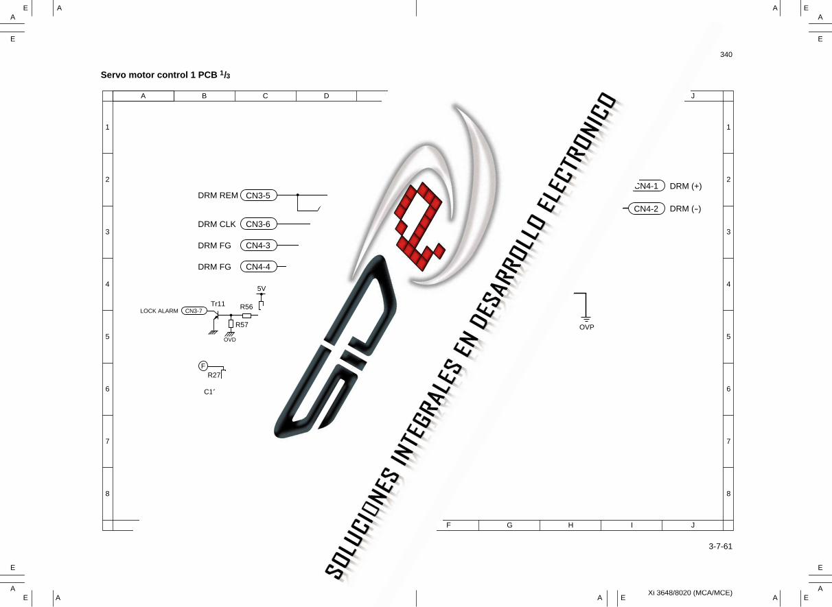
AA A
A
AA A
A
E
E E
E
E
E E
E
EA
EA
Xi 3648/8020 (MCA/MCE)
A B C D E F G H I J
A B C D E F G H I J
1
2
3
4
5
6
7
8
1
2
3
4
5
6
7
8
340
3-7-61
Servo motor control 1 PCB 1/3
CN3-5CN4-1
CN3-6
CN4-3
CN4-4
CN3-7LOCK ALARM
G
H
F
F
G
E
E
E
206 12
11
18
19
15
OVD
OVDOVP
ST Cout
TP2-1
IC2
Dout Pout FBout ADD
5V
5V
5V
PWM
CL
RE
CLOCK
FG
FG
GND
TP2-2
17
5V24V
CN4-2
D3
Q2
D4
R19
R18
R20
C11
OVD
1
2
3
910716
OVDR33
R32
R31R30
C14
R34
R28R27
Tr7Tr10
Tr9
Tr5
Tr6
R55C15
C13 OVD
OVDOVD
OVD
OVD
R21 R22R23 R24
R35
C12
C10R25 R26
OVD
OVD
OVD
OVD
OVD
OVD
R57
R56
OVD
+
5V
5V
5V
Tr11
OVDOVD
R29
C15
C16
DRM REM
DRM CLK
DRM FG
DRM FG
DRM (+)
DRM (-)

AA A A
A
AA A A
A
E
E E E
E
E
E E E
E
A B C D E F G H I J
A B C D E F G H I J
1
2
3
4
5
6
7
8
1
2
3
4
5
6
7
8
Xi 3648/8020 (MCA/MCE)
3-7-62
340
Servo motor control 1 PCB 2/3
CN3-1CN1-1
CN3-2
CN1-3
CN1-4
C
D
B
B
C
A
D
A
206 12
11
18
19
15
OVD
OVDOVP
ST Cout
TP1-1
IC1
Dout Pout FBout ADD
5V
5V
5V
PWM
CL
RE
CLOCK
FG
FG
GND
TP1-2
17
5V
OVP
CN2-1
CN1-2
CN2-2
24V
5V
D1
C1
F1
Q1
D2
R2
R1
JP1
OVP
CN2-3NC
CN2-45V
CN2-5OVD
24V
R3
C5
CX1~3 C3 C2
OVD
1
2
3
910716OVD
OVD
OVDR16
R15
R14R13
C8
R17
R12R11R10
Tr3
Tr1
Tr2
R54C9
C7OVD
OVDOVD
OVD
OVD
R4 R5R6 R7
C6
C4R8 R9
OVD
OVD
OVD
+
5V
5V
OVDOVD
DM REM
DM CLK
DM FG
DM FG
DM (+)
24V
DM (-)
5V
GS
GP

AA A
A
AA A
A
E
E E
E
E
E E
E
EA
EA
Xi 3648/8020 (MCA/MCE)
A B C D E F G H I J
A B C D E F G H I J
1
2
3
4
5
6
7
8
1
2
3
4
5
6
7
8
340
3-7-63
Servo motor control 1 PCB 3/3
CN3-3FDM REM
FDM CLK
FDM FG
FDM FG
CN5-1 FDM (+)
FDM (-)
CN3-4
CN5-3
CN5-4
K
L
J
J
K
I
L
I
206 12
11
18
19
15
OVD
OVDOVP
ST Cout
TP3-1
IC3
Dout Pout FBout ADD
5V
5V
5V
PWM
CL
RE
CLOCK
FG
FG
GND
TP3-2
17
5V
CN5-2
24V
D5
Q3
D6
R38
R37
R39
C18
OVD
1
2
3
910716
OVDR52
R51
R50R49
C21
R53
R48R47R46
Tr14
Tr12
Tr13
R58C22
C20 OVD
OVDOVD
GD
OVD
R40 R41R42 R43
C19
C17R44 R45
GD
GD
GD
+
5V
5V
GDGD

AA A A
A
AA A A
A
E
E E E
E
E
E E E
E
A B C D E F G H I J
A B C D E F G H I J
1
2
3
4
5
6
7
8
1
2
3
4
5
6
7
8
Xi 3648/8020 (MCA/MCE)
3-7-64
340
Output PCB
CN5-7
CN6-1
GND
24V
CN4-3 24V
CN7-1 24V
CN7-2 24V
CN1-124VR
CN1-2
CN3-3
CN3-424VR
CN1-3
CN1-4
CN2-124VR
CN2-2
CN3-1
CN3-224VR
CN2-3
CN1-5
CN2-4
CN4-1 GND
CN5-6CN6-7
CN6-8
CN5-5CN6-6
CN5-4CN6-5
8
CN5-3CN6-4
CN5-2CN6-3
CN5-1CN6-2
CN6-9
R11 16
2 15
3 14
4 13
5 12
6 11
7 10
R2
R3
R4
R5
R6
R7
R8
R9
R10
R11
R12
R13
R14
R15
R16
R17
R18
R19
R20
R21
TR1
TR2
TR3
TR4
TR5
TR6
TR7
PCHL REM
RTL REM
FLH REM
DH REM
RH-U REM
RH-M REM
RH-L REM
PCHL
RTL
FLH
DH
RH-U
RH-M
RH-L

AA A
A
AA A
A
E
E E
E
E
E E
E
EA
EA
Xi 3648/8020 (MCA/MCE)
A B C D E F G H I J
A B C D E F G H I J
1
2
3
4
5
6
7
8
1
2
3
4
5
6
7
8
340
3-7-65
LPH power supply PCB
P4
1
2
3
C2
+
NC
-
CN-AD1
D2
D3
T1 2/3
C5
F1
C1
L1
C3 C4
C9
C8
R1
R2
R3
C26
+ +
P3
R4 R6
R5
R7
Q1
+ +
D4
D5
D8
C27 C28
R9
R25R23
R22
R10
R15
R16
R17
D7 D6C10 R12
Z3 2/2C11
C12
+
C14
R14
C13
R13
Z2 2/2
Z18
1 2 3 4
7 6 5
R11
P1
P2
T1 3/3
C6
C23
R8
R30R28R24
C7
S1
L3
D9
L4
R19
C18 C19
C17
R18 C15 C16
T1 1/3
+
C20 C21R20
+ +
L2
Heat sink
Heat sinkZ2 1/2
Z4
R21
RV1
C22
R26
CN-V
R32
D10
TS1
Z3 1/2
R31R27
Z5
R29
C24
L5
C25
+
CN-B
1234
5678
+5V
GND
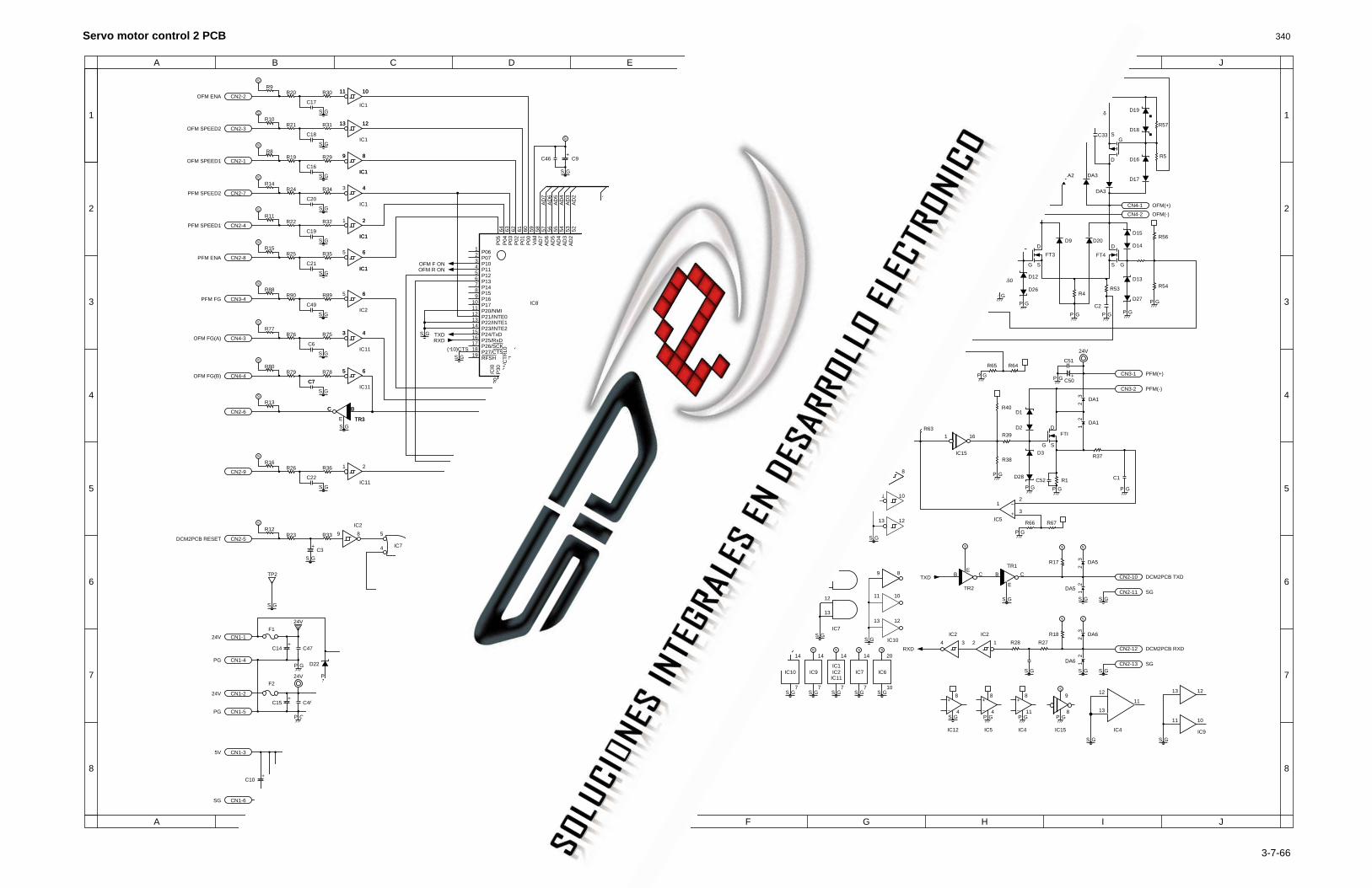
A B C D E F G H I J
A B C D E F G H I J
1
2
3
4
5
6
7
8
1
2
3
4
5
6
7
8
3-7-66
340Servo motor control 2 PCB
P G
S
OFM ENA
S
OFM SPEED2
IC1S
OFM SPEED1
R8R19
IC1C16
S
PFM SPEED2
R14R24 R34
IC1C20
S
PFM SPEED1
R11R22 R32
IC1S
PFM ENA
R15R25 R35
IC1C21
S
PFM FG
R88R90 R89
C49
S
OFM FG(A)
R77
S
OFM FG(B)
R80
C7
S
R13
S
R16R26 R36
C3
C22
C B
E
S G
S
S G
S G
S G
S G
S G
S G
S G
S G
S G
S G
S G
S G
S G
S G
S G
S
S G
+
S G
+
S G
S
S G
S
S
S G
S
S G
S G
–
+
–
+
–
+
S
S G S
S G
S
S G
P G
24V
S
S
SS
S
P G
–
+
P G
PFM(+)
PFM(-)
P G P G P G
–
+
P G
DCM2PCB TXD
SG
B C
S G
E
B CE
S S S
S G S G
DCM2PCB RXD
SG
S S
S G S GS G
+
–S G
8
4
+
–
8
4
+
–
8
11P G P G
S
S G
14
7
S
S G
14
7
S
S G
14
7
S
S G
14
7
S
S G
20
10
S
S G S G S G
–
+
OFM F ON
OFM R ON
SS
P G
P G
P G
P G
P G P G
S
S
–
+
S
S G
24V
S
S
S
R12R23 R33
S
S G
+
S G
S G
+
P G
24V
S G
+
S
S G
+
S
S G
S
+ +
+
P G
+
P G
S G
P G
+
OFM F ON
21
3456789
101112131415
19181716
20
OFM R ON
TXDRXD
( 10)CTS*
P07P06
P10P11P12P13P14P15P16P17P20/NMIP21/INTE0P22/INTE1P23/INTE2P24/TxD
RFSHP27/CTSP26/SCKP25/RxD
21 22 23 24 25 26 27 28 29 30 31 32A
Vss
/CI0
P30
P31
/CT
RL0
P32
/CI1
P33
/CT
RL1
X1
X2
Vss
AN
0A
N1
AN
2A
N3
AV
ref
64 63 62 61 60 59 58 57 56 55 54 53A
D2
P05
P04
P03
P02
P01
P00
Vdd
AD
7A
D6
AD
5A
D4
AD
3
52
AD
7A
D6
AD
5A
D4
AD
3A
D2
AD
1A
D0
RESET
5150494847464544 A1543 A1442 A1341 A1240 A1139 A1038 A9
34353637 A8
AD0AD1
ALEWRRD
RESETEA
A15A14A13A12A11A10A9A8
PWM0/P34PWM1/P35
TO0/CLR0/P36TO1/CLR1/P37
33
AD0 3AD1 4AD2 7AD3 8AD4 13AD5 14AD6 17AD7 18
111
D1D2D3D4D5D6D7D8
C-EN-OC
2 A05 A16 A29 A312 A415 A516 A619 A7
Q1Q2Q3Q4Q5Q6Q7Q8
1A12 2A7 3A6 4A5 5A4 6A3 7A2 8A1 9A0 10
AD0 11AD1 12AD2 13
14
2827 A1426 A1325 A824 A923 A112221 A1020 A1519 AD718 AD617 AD516 AD415 AD3
VPPA12A7A6A5A4A3A2A1A0D0D1D2GND
VCCA14A13A8A9
A11OE
A10CED7D6D5D4D3
GS
D
GS
D
S
D
G S
D
G
CN4-1 OFM(+)
CN4-2 OFM(-)
G S
D
23
12
12
23
12
23
F ON
TXD
RXD
32
12
CN1-3
CN1-6
CN3-3PCM 5V
CN3-5PCM SG
CN4-5SM 5V
CN4-6SM SG
CN1-124V
CN1-4PG
CN1-224V
CN1-5PG
5V
SG
DCM2PCB RESET
CN2-2
CN2-3
CN2-1
CN2-7
CN2-4
CN2-8
CN3-4
CN4-3
CN4-4
12MHz
VCC
GNDOut
I OG
CN3-1
CN3-2
CN2-10
CN2-11
CN2-12
CN2-13
CN2-9
CN2-5
CN2-6
RESET
2
1
3
24V
24V
TR3
11 10
13 12
9 8
3 4
1 2
5 6
5 6
3 4
5 6
IC11
1 2
IC2
9 8 5
4 IC76
1
2 IC73
IC2
10 11
IC2
12 13 R41D21
R42C4
R43
R9R20 R30
IC1C17
R10R21 R31
C18
R29
IC1
IC1C19
IC1
IC2
R76 R75
IC11C6
R79 R78
IC11C7
C B
TR3
11 10
13 12
9 8
4
2
6
6
3 4
5 6
IC3
TP2
F1
C14 C47
F2
C15 C48
D22
D25
TR15
R109
R108C10 C44
D24
R110
C45 C11
C8
C13
R87
R7 TR14
C41 C40 C12
D23
IC13
IC8
X1
C30 C29
C5
R97R91R92
R103R95R96R94R93
TP1
R81
C36
C46 C9
R107
JP1
IC14
C43
IC6
R104R105R106R102R101R100R99R98
R45
R44DA4
C28IC4 IC4
89
10
R48
D5
IC4
76
5
R47
R46
C27
DA4
C24
C25 C35 C38
C31 C37 C42
C39 C26 C32
IC10 IC9 IC2 IC7 IC6IC1
IC11
IC12 IC5 IC4
IC2
4 3
IC2
2 1
R28 R27
R18 DA6
R17 DA5
R67R66IC5
12
3
TR1
TR2
R1
D3
FTI
DA1
DA1
R37
C1
R64R65
R40
R391 16
IC15
3 410
R73 R63
R38
5 610
5 69
R68
R74
76
5
IC5
R82
3 49
1 29
9 89
1 210
R71 R72 R70 R69
4 13
IC15
3 14
IC15
R50
R51
R52
D11
D10
FT3
D9 D20
FT4
R4R53
C2
D26
D12
R54
R56
D14
D15
D27
D13
DA2 DA3
DA3
D17
DA2
D16
D8
D7R3
R49
R2 R6
C23 C33D18
D19
R57
R5
D6
D4
2 15
IC15
5 12
IC15
R83
R84
5
67
IC12
3
21
IC12
R85
R86
D1
D2
D28
9
12
IC7
10
13
S GS G
S G
9 8
11 10
13 12
13 12
11 10
9 8
IC10
IC11
9
8
S
S G S G
12
13
11
IC4
11 10
13 12
IC9
DA5
DA6
IC15
FT2
P G
+
C51
C50
C52
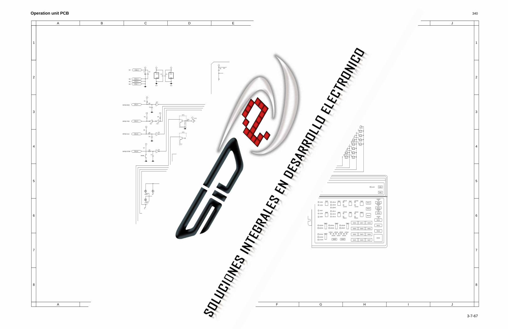
A B C D E F G H I J
A B C D E F G H I J
1
2
3
4
5
6
7
8
1
2
3
4
5
6
7
8
3-7-67
340Operation unit PCB
LED1LED4
LED5SW3
LED10
LED42
LED6
LED43
LED11
LED12
LED13
LED6
LED7
LED8
LED9
LED14
LED15
LED16
LED17
LED18
LED19
LED20
LED21
LED29
LED30
LED41
LED26
LED34 LED36
LED35 LED37 LED39
LED38 LED40
LED28
LED27
LED31
LED32
LED33
LED2
LED3
SW5 SW7 SW9
SW12
SW11 SW16
LED23
SW1
SW2
SW17
SW18
SW14
SW15
SW19
SW38
SW13
SW4
SW22
SW25
SW20 SW21 SW26 SW27 SW28
SW24SW23
SW6 SW8 SW10
SW29 SW30 SW31
SW32 SW33 SW34
SW35 SW36 SW37
LED24
LED25
LED22
LED14
LED22
LED29
LED37
LED5 LED4 LED3
4 4
LED2 LED1
(1/1)LEFT PCB
R12DT4
DT3
R1
C1 C2
IC3 IC4
C3 C4VCC
GND
VCC
GND
14
7 7
6
5 4 3 2 1 42 41 40 39 38
17 18 19 20 21 22 23 24 25 26
7
8
9
10
11
12
13
14
15
16
37
14
2
4
5
6
3
1
13121110987
36
35
34
33
32
31
30
29
28
27
14
R2IC4
IC3
C5
IC4
IC4
IC4
R3
R5
R7
SW38
R4
RIGHT PCB (2/2)
LED13
LED21
LED28
LED36
LED43 LED42 LED41 LED40 LED39 LED38
R21
R61
R22
R62
R23
R63
R24
R64
R25
R65
R26
R66
R27
R67
R28
R68
LED12
LED20
LED27
LED35
LED11
LED19
LED26
LED34
LED10
LED18
LED33
LED9
LED17
LED25R G
LED32
LED8
LED16
LED24
LED31
LED7
LED15
LED23
LED30
DT28DT27DT26DT25DT24DT23DT22DT21
LD7
LD6
LD4
LD3
LD2
LD1
LD0
LD5
R14DT6
DT5
R16DT8
DT7
R10DT2
EMC
C9
C8
R29
RS
LCD MODULE
C15
Vdd
V0
Vss
R/W
E
D0
D1
D2
D3
D4
D5
D6
D7
RSP81
P80
3
4 5
1GND
RS
Key4
Dig5
Dig4
P81
P80
SB1
SB0
SCK
Stop Key
Key3
P50
P51
P52
P53
P60/KR0
P61/KR1
P62/KR2
P63/KR3
P70/KR4
P71/KR5
P72 /KR6
Key
2
Key
1
Key
0
NC
VD
D
Dig
3
Dig
2
Dig
1
Dig
0
P73
/KR
7
X2
X1
RE
SE
T
XT
2
XT
1
VS
S
P40
P41
P42
P43
OUT
Vdd
IC2
DT1
CN1-2
CN1-6
CN1-8
CN1-4
CN1-1
CN1-7
CN1-5
CN1-3
OPCB RXD
IC1
SG
SG
SG
SV
OPCB TXD
OPCB CLK
OPCB STOP
C6
C7
C13
R6
R8
+
R18
DT10
DT9
R51R56
R20 DT12
DT11
R52R57
R53R58
R54R59
R55R60
R35
C14
LD4
LD0
LD1
LD2
LD3
LD5
LD6
LD7
R30
R31
R32
R36
R431
2 SW1
RIGHTPCB
(1/2)
SW2
SW3
SW4
SW5
SW6
SW7
SW8
R44
R45
R46
R47
R48
R49
R50
R37
DT14
R38
R39
R40
R41
R42
DT13
DT15
DT16
DT17
DT18
DT19
DT20
SW9
SW10
SW11
SW12
SW13
SW14
SW15
SW16
SW17
SW18
SW19
SW20
SW21
SW22
SW23
SW24
SW25
SW26
SW27
SW28
SW29
SW30
SW31
SW32
SW33
SW34
SW35
SW36
SW37
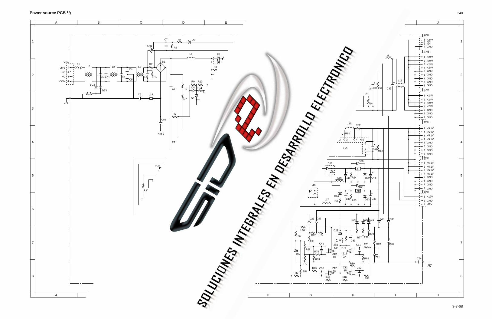
A B C D E F G H I J
A B C D E F G H I J
1
2
3
4
5
6
7
8
1
2
3
4
5
6
7
8
3-7-68
340Power source PCB 1/2
NC
NC
LIVE
COM
D1
F1L1
D2
Z1
11 14
12 13 8 7 4 6 5
9 10 1 2 3R44
L2
CN1
1
2
3
4
L3
C1BG1
BG2
BG3
E1
C2
C4
C5
C6 L18
R1
D1R2
C3
CR1
C7 R4
R3
L4
C8 R6
R7
R5
C56
H.B 2 H.B A
C57
R9 R10
D4 R11
D5
R12 R13
Q1Q2
C11
C12
R14
C13
R8 C9 C10
L5TP1
R15
R16
R27
R28
R29
R30
C20
R32
R31
TB1RV1
R43
R42
R41
U-2
R40+
C26R37R36
Z5 1/2
Z2 2/2 Z9 2/2
Z5 2/2
R91 R39
R38
R90
C22
C23
+R33
D11
R34 R35
C24+ C25
R24 D6
Z2 1/2
C55
R45
D9
Z3 2/2
Z10 2/2
5 3 2 7 5 4
10 9 8 1
+-
+-
+-
+-
+-
+-
C15D6
T1 2/3
T1 /1/3
C16
C17
R23
Q4R18
R19 Q3
D7
R17
C14
+
TP2
R20 R21
R22
C18
Z4
C19
R26
Z3 1/2
C21
T1 3/3
D10
R88R87R86
R83 R84R85 C50 Z12
3/4
Z12 4/4
C52
R89
UV UV
UV UV
R74
R70
R75
C49
Z12 1/4
Z12 2/4
R82
R81 R80
Z11
C51
+R72 R73
D28
R71
R68
R67
R68
D27
Z10 1/2 R76
C53R77 R78
R79
+
C48
D33D32D31D30D29D26D25
+
C45D23
Z8
Z7
D21
R65
D24+
C46R66L17
D19
D18D20
+
L16 C44 R64 D22 C45
+
+ +
U-3
1 2 3 4 5
6
7
+
R63C43
C41
C42
R60D17
C40C37
L14
R61
Q5L15
R62L13
L11L9
D13
R49
C34
C33 D16
C32C31R48
L8
R46 C27 C28
C29
C30
R47L10
L7
D12
L6
Z9 1/2
R50
L12
R51
R52D14
R53 D15
RV2
L13+
C39
CN2
+24VNCNCGND
CN3
CN4
CN5
CN6
CN7
R59C38R57
R55
Z6
C35 R54 +
+
C36
R56
1234
+24V
+24V+24V
GND+24V
+24V
+24V+24V+24V
+5.1V
+5.1V
+5.1V+5.1V+5.1V
+12V
-12V
+5.1V+5.1V
+5.1V
GND
1
23456
GND7
1
23456
7
1
23456
7
8
1
23
1
23
456
7
8
GND8GND
GNDGND
GND
GND
GND
GND
GND
GND
GNDGND
GND
GND
9
C54
+
+

A B C D E F G H I J
A B C D E F G H I J
1
2
3
4
5
6
7
8
1
2
3
4
5
6
7
8
3-7-69
340Power source PCB 2/2
D1
45723
C4
6
CN1
R1
R2
R3
C1
+
Q2
R9R8
C5
R11
R10 R12
C6
R13
R14 C7
+
78 6 5 4 3 2 1
109 11 12 13 14 15 16Z1
C8
+
C9 R15 R18
R17
R16
RV1
R7
R4
R5
C3
R6C2
Q1
10 9 8 1
D1
D2
D3
1 2 3 4 5 6
7
C3
C8
C6
C5
CN1
9 10 11 12 13 14 15 16
8 7 56 4 3 2 1Z1
8 7 6 5
1 2 3 4Z1
C7
RV1
R1 R2
R12
R7
R8 R9
R15
R14
R17
R18
R11
R16
R19
R13
R10
R3
R4
R5 R6
C2
C4
C1
Q1
+
+

A B C D E F G H I J
A B C D E F G H I J
1
2
3
4
5
6
7
8
1
2
3
4
5
6
7
8
3-7-70
340
1
2
RD
YW24VR
RTL REM
RD
BE
1
2
3
4
5
6
RD
YW
OE
PK
BE
PE
RD
YW
OE
GN
BE
WE
RD
YW
WE
BE
GN
OE
1
2
3
1
2
3
24VR
PCFM
PCFM H/L
RTL
PCFM
PCSW
FTH3
FTH4
BYPTIMSW
STHVT
BYPRSW
GS
PCSW
5V
LB
GN
OE
RD
BK
BE
YW
BE
GY
BE
1
2
3
4
FTH3
GS
FTH4
GS
YW
BE1
2
BK
BK
YW
BE1
2
BK
BK
OE
PE
BE
1
2
3
1
2
3
OE
GY
BE
5V
BYPTIMSW
GS
RD
BE
YW
YW
GN
GN
BE
RD
BE
YW
YW
GN
GN
BE
1
2
3
4
5
6
7
YW
YW
GN
RD
BE
1
2
3
4
5
6
TC REM
SC REM
ST ALARM
24VR
GP
GN
BK
YW
RD
BE
RD
BE
GN
BK
YW
1
2
3
4
5
BLACK
GRAY
YELLOW
GREEN
BLUE
WHITE
PINK
RED
ORANGE
LIGHT BLUE
PURPLE
BK
GY
YW
GN
BE
WE
PK
RD
OE
LB
PE
BE
GN
1
2
3
4
GS
BYPRSW
BK
BK
1 2 3 4 5 6 7 8 9 10
11
12
13
14
15
16
17
18
19
20
21
22
23
24
BK
PE
YW
YW
BE
GY
PE
GN
OE
YW
BK
YW
PK
PE
BE
YW
YW
GN
RD
1 2 3 4 5 6 7 8 9 10
11
12
13
14
15
16
WE
BE
PE
GN
YW
RD
WE
YW
BE
GY
GN
YW
C10
2
C10
1
AC
(L)
FF
M H
/L
R-L
amp
RE
M
FT
H1
GS
FT
H2
ES
W
EP
S
5V
FF
M-R
•FF
M-L
AC
(L)
PC
FM
PC
SW
PC
FM
H/L
GP
TC
RE
M
SC
RE
M
ST
ALA
RM
24V
R
H1
GS
BY
PT
IMS
W
BY
PR
SW
OS
SW
1
24V
R
H2
FT
H3
GS
FT
H4
OS
SW
2
RT
L R
EM
WE
WE
WE
FT
SW
2
145˚
C/2
93˚F
145˚
C/2
93˚F
FT
SW
1
WE
WE
H1
H2
WE
WE
BK
1 1
1 1
BK
BK
1 2
GY
GY
BK
BK
1 2
GY
GY
BK
BK
1 2 3 4
FT
H1
GS
FT
H2
GS
YW
BE
GY
BE
1 2
GS
ES
W
BE
PE
1 2 3
1 2 3
1 2 3
5V
FP
S
GS
OE
YW
BE
OE
GN
BE
RD
BK
BE
RD
BK
BE
24V
R
FF
M-L
FF
M-L
H/L
1 2 3
RD
BK
BE
RD
BK
BE
24V
R
FF
M-R
FF
M-R
H/L
1 2 3 4
1 2 3
1 2 3
1 2 3
1 2 3
1 2
RD
BK
BE
GN
RD
YW
PE
YE
24V
R
R-L
amp
RE
M
RD
GN
5V
OS
SW
1
GS
5V
OS
SW
2
GS
OE
YW
BE
OE
YW
BE
OE
YW
GN
BE
OE
YW
GN
BE
1 2 3 4 5
OE
GN
BE
OE
GN
BE
OSSW2OSSW1
R-Lamp
FFM-L
FPS
FFM-R
ESW
FTH1 FTH2
1 1
1 1
Detachable unit wiring diagram

A B C D E F G H I J
A B C D E F G H I J
1
2
3
4
5
6
7
8
1
2
3
4
5
6
7
8
General connection diagram 340-3
3-7-71
E
E
A
A
E
A
E
A
A
E
E
A
E
A
E
A
1
2
3
4
5
6
7
5V
GS
12V
GS
-12
C17C11C19C20
C6
C5
C1C2C3C4
C7
(OR C12)
1 601 100
C15
C16
C14
C13
C4-10A
C3-1
C4-11A
C2-12
C2-11
C2-14
C2-13
1
2
3
4
1
2
3
4
1
2
1
2
3
4
KC COUNT
24VR
KC DET
GS
TC COUNT
24VR 24VR
24V
DH
FLTH
GS
24V
FLH REM
24V
24V
X
W
1 2 3 4 5 6 7 8 9
1 2 3 4 5 6 7
1 2 3 4 5 6
1 2 3 4 5 6 1 2 3 4 5
1 2 3 41 2
1 2 3 4 5 6 7 8 1 2 3
T U V W X Y Z GP
24V
CN6
CN5CN3
CN724VR
24VR
24VR
24VR
24VR
1
2
3
4
5
24VR
24VR
24VR
24VR
1
2
3
4
CN2
CN1
1 2 3 4 5 6 7 8 9 10 11 12 13
CN43
2
1
2
1
4
3
2
1
24V(H)
GP(H)
24V(H)
24V(H)
24VR
24VR
CN4
CN2
CN1DCM2PCB
CN31
2
3
4
5
6
OFM
(+)
OFM
(-)
OFM
A
OFM
B
5V
GN
D
24VR
5V
GP
GS
GP
24VR
24V
R
OFM
SP
EE
D1
OFM
EN
A
OFM
SP
EE
D2
PFM
SP
EE
D1
DCM
2PCB
RES
ET
PFM
SP
EE
D2
PFM
EN
A
DCM
2PCB
TXD
GS
DCM
2PCB
RXD
GS
C8-
1
C8-
2
C8-
3
C8-
4
C8-
5
C8-
6
C8-
7
C8-
8
C6-
20
SS
W1
SS
W2
C3-
23
C3-
24
C3-
25
C3-
26
C3-
27
C3-
28
C3-
29
C3-
30
C3-
31
C3-
32
C3-
33
C3-
18
C4-
15A
C4-
14B
C4-
14A
C4-
13A
C4-
13B
C4-
12B
C4-
12A
PFM
(+)
PFM
(-)
5V
PFM
FG
GN
D
SV
OP
CB
TX
D
GS
OP
CB
RX
D
GS
OP
CB
CLK
GS
OP
CB
STO
P
1
2
3
4
5
6
7
8
LPH
C22
C21
GS
GS
GS
GS
5V
5V
5V
5V
L
N
F.G
1 2 3 4 1 2 3 4
1 2 3 4
1 2
1 2 31 2 3 4 5 6 7
1 2 3 4 5 6 7 8 9 1 2 3 4 5 6 7 8
1 2 3 4 5 6 7 8
1 2 3
1
2
3
4
5
6
7
8
1
2
3
5V
5V
5V
5V
GS
GS
GS
GS
+12
GS
-12V
24V
GP
L N 24V
24V
24V
24V
GP
GP
GP
24V
24V
24V
24V
GP
GP
GP
GP
GP
5V
5V
5V
5V
GS
GS
GS
GS
CN6CN3
CN2 CN1 CN4
CN
7
SS
W6
SS
W3
SS
W4
CN
5
GS
RH-L
REM
RH-M
REM
RH-U
REM
DH R
EM
FLH
REM
RTL
REM
PCHL
REM
S
Z
2 1 2 1 2 1
5V 5V 5V
SS
R3 *
2
24VR
24VR
LPH
L
N
L
N
24V
GP
5V
5V
5V
5V
GS
GS
GS
GS
S2 S3
S1 S4
S2 S3
S1 S4
SS
R2
SS
R1
4 3 2 1
1
2
3
4
C4-
16B
C5-
1
C5-
2
C5-
3
C5-
4
C5-
5
C5-
6
C5-
7
C1-
1
C1-
2
C4-
17B
C4-
17A
C4-
16A
C4-
8B
C4-
7B
C4-
3A C4-5A
C4-5B
C4-9B
C2-5
C2-3
C2-6
C3-16
C3-17
C4-6A
C3-15
C4-6B
C4-1B
C4-2B
C3-3
C3-14
C3-34
C2-7
C2-4
C2-8
C3-21
C3-22
C1-1
C1-13
C2-1
C2-9
C1-12
C1-4
C1-5
C1-6
C1-7
C1-8
C1-9
C1-10
C1-16
C1-11
C1-17
C1-18
SV
24VR
GP
C1-24
C1-19
C1-20
C1-21
C1-22
C2-6
C2-4GS
C2-5
C2-12
C2-13
C2-14
C2-7
C2-15
24VR C2-8
C2-16
1
2
3
4
1
2
3
4
1
2
3
1
2
3
1
2
3
1
2
3
4
5
6
1
2
1
2
3
4
5
6
1
2
3
4
5
6
7
1
2
3
4
1
2
3
1
2
3
1
2
3
4
1
2
1
2
1
2
3
4
1
2
1
2
3
4
5
6
1
2
3
1
2
3
1
2
3
1
2
3
1
2
1
2
24VR
FFM-R
FFM-R H/L
24VR
FFM-L
FFM-L H/L
24VR
R-Lamp REM
FTH1
GS
1
2
FTH2
GS
GS
ESW
5V
FPS
GS
24VR
RCFM
H/L
GS
PCSW
5V
TC REM
SC REM
ST ALARM
24VR
GP
GS
BYPRSW
5V
BYPTIMSW
GS
FTH4
GS
FTH3
GS
5V
OSSW1
GS
5V
OSSW2
GS
24VR
RTL REMY
C6-
9
C4-
8A
C4-
9A
C3-
19
C3-
20
C3-
10
C3-
9
C3-
4
C3-
5
C6-
10
C6-
11
C7-
16
C6-
8
C3-
6
C6-
12
C6-
13
C7-
17
C7-
15
C7-
20
C7-
21
24V
R
24V
R24
VR
FCL-
M
24V
R
RW
CL-
M
24V
R
CC
L
24V
R
FCL-
L
24V
R
RW
CL-
L
24V
R
24V
R
24V
R
24V
R
24V
R
RP
CC
L
5V
GS
5V
PS
-L
GS
5V
GS
5V
GS
5V
PS
-M
GS
5V
RLD
SW
-L
GS
5V
PS
SW
1-L
GS
5V
PS
SW
2-L
GS
1 2 3 4 5 1 2 3 4 5
1 2 3 4 5
1 2 31 2 31 2 31 2 31 21 2
1 2
1 2 3 1 2 3 1 2 3 1 2 3 1 2 3 1 2 3
1 2 31 2 3 1 2 3 1 2 1 21 21 21 2
1 2 3 4 5 6 7 8 9 10 11 12
1 2 3 4 5 6 7 8 9 10 11 12 1 2 3 4 5 6 7 8 9 10 11 12 1 2 3 4 5 6 7 8 9 10 11 12
1 2 3 4 5
1 2
1
2
24V
RH-U REM
V
U T
24V
R
FCL-
U
24V
R
RW
CL-
U
24V
R
24V
24V
RH
-M R
EM
24V
PH
-L R
EM
24V
5V
PS
SW
1-U
GS
5V
PS
SW
2-U
GS
5V
PS
-U
GS
5V
RLD
SW
-U
GS
5V GS
GS
24V
GS
C7-
14
C7-
18
C7-
19
C7-
13
C7-
12
C6-
5
C6-
4
C6-
6
C6-
3
C6-
2
C6-
1
C6-
14 C6-
7
C6-
18
C7-
22
5V
GS
5V
GS
5V
GS
5V
CH
PS
W2
GS
5V
CH
PS
W1
GS
24V
R
CFM
24V
R
24V
R
LPH
FM
24V
R
24V
R24
VR
BY
PR
CL
24V
R24
VR
RC
L
1 2 3 1 2 3 1 2 3 1 2 3
1 2 3 1 2 3 1 2
1 2 1 2
1 2 3 4 5 6 7 8 9
1 2 3 4 5 6
4 3 2 1
F.G
F.G
FL
S5V
RLD
SW
-M
GS
5V
PS
SW
1-M
GS
5V
PS
SW
2-M
GS
24V
R
24V
R
24V
R
CS
OL1
24V
R
CS
OL2
24V
R
SS
OL
24V
R
PC
HL
24V
R
GP
24V
R
GP
FL R
EM
FL C
ON
T
C7-
4
C7-
5
C7-
6
C7-
7
C7-
1
C7-
2
C7-
8
C6-
17
C7-
23
C6-
19
C4-
3B
C4-
4B
C2-
19
C2-
18
C2-
17
C2-
1
C2-
2
C4-
1A
C4-
2A
C2-
16
C2-
15
C2-
9
C2-
10
C3-
12
C3-
13
C3-
7
C3-
8
C4-
7A
C3-
11
C7-
11
1 2 3 4 5 6 7 1 2 3 4 5
1 2 3 4 5 6 7 1 2 3 4 5 6 1 2 3 41 2 31 2 3 4 5
3 2 1 1 2
1 2 3 4
1 2 3 4 5
1 2
1
2
1
21 2 3
1 2 3 4 1 2 3 4 1 2 3 4
CN3 CN2
CN1 CN4 CN5
F.G
24VR24VR
OFCL
GS
GS
24V
R
GP
24V
R
GP
MC
RE
M
GR
ID C
ON
T
MC
ALA
RM
1 2 3 4 5
24V
R
GP
24V
R
GP
DB
RE
M
DB
CH
G
DB
CO
NT
24V
24V
TNS
GS
GS
DTH
24V
DP
S
GS
GP
GS
ETT
H
24V
GP
5V
GS
5V
OLD
SW
GS
5V
OTD
SW
GS
1 2 3
5V
GS
GS
GS
TDTD
SW
GS
OFS
24V
R
GP
5V
GS
24V
R
GP
5V
GS
DM
RE
M
DM
CLK
FDM
RE
M
FDM
CLK
DR
M R
EM
DR
M C
LK
LOCK
ALA
RM
DM
(+)
DM
(-)
DM
FG
DM
FG
DR
M(+
)
DR
M(-
)
DR
M F
G
DR
M F
G
FDM
(+)
FDM
(-)
FDM
FG
FDM
FG
1 42 3
1 42 3
2 41 3
1
12
2
1
BUPCB
ISUPCB
INTERFACE
CONTROLLER
(OPTION)
MEMORY
UNIT
(OPTION)
CIS UNIT
LPHROMPCB
OPCB
PRY3
OFM PFM
OPPCB
PSPCB ISUPCB
SSW5
PRY2
PRY1
LPHPSPCB
FTSW1
145˚C/293˚F
FTSW2
145˚C/293˚F
H1 H2
DETACHABLE UNIT
TNS DTH
DBHVT
DB
TM
DEVELOPING UNIT
DPS
DPSPCB
ETTH
OFCL
RSW
OHSW
OLDSW OTDSW TDTDSW OFS
RTL
OSSW1
OSSW2
FTH4
FTH3
BYPTIMSW
BYPRSW
STHVT
PCSW
PCFM
ESW
FPS
FTH2
FTH1
R-Lamp
FFM-L
FFM-R
MC GRID
DCM1PCB
INPCB
CFM BYPRCL
C6-
1524
VR
RE
M
24V
R
1 2
LPHFM2 RCLLPHFM1
DM DRM FDM
MPCB
KC
(OPTION)
TC
24VR
GS
DH
FLTH
FLH
RPCCLFCL-M RWCL-M PS-M CCL FCL-L*1 RWCL-L*1 PS-L*1
RLDSW-L*1 PSSW1-L*1 PSSW2-L*1
*1: OPTION *2: 230 V, 50 Hz models only.
RLDSW-M PSSW1-M PSSW2-M
CHPSW2 CHPSW1
PCHLSSOLCSOL
CLEANING UNIT
RH-U
RHSW-U
FCL-U RWCL-U PSSW1-U PSSW2-U PS-U RLDSW-U
FIRST ROLL UNIT
SECOND ROLL UNIT THIRD ROLL UNIT (OPTION)
RHSW-M RHSW-L
RH-M RH-L
NF
21
S2 S3
S1 S4
1 2
FR*2
24V
C4-
4A
CN2
DRPCB
CN1
1
2
3
4
L
N
1
2
3
GP(H)
24V(H)
1
2
3
4
+ –
L
N
L
N
MSW
L
N
L
N
DRSW
1
2
3
1
2
3
L
N
F.G
MEMORY UNIT (OPTION)
MPCB
(C19)
1 2 3

A B C D E F G H I J
A B C D E F G H I J
1
2
3
4
5
6
7
8
1
2
3
4
5
6
7
8
General wiring diagram 340-3
3-7-72
E
E
A
A
E
A
E
A
A
E
E
A
E
A
E
A
PK
PE
OE
YW
BE
1
2
3
4
5
6
1
2
3
4
(R.M)
PFM(-)
PFM(+)
5V
PFM FG
Gs
ETTH
Gs
Gp
Gs
DPS
24V
(JC6)
(JC4)
(JC) JUNCTION CONNECT
1 2YW
BE6
5
4
3
2
1
BE.C1-4(SP.P)
BE.C1-3(SP.P)
YW.C1-2(SP.P)
YW. -9(C.U)
RD. (LD.SSW)
RD. -1 (H.SSW)
RD.C1-1(SP.P)
PK.C3-2 (ORM.P)
PE.C3-1 (ORM.P)
OE.C3-3 (ORM.P)
YW.W15
BE.C3-5(ORM.P)
YW.C2-10(M.P)
BE.C2-9(M.P)
BE.W14
BE.C2-15(M.P)
YW.C2-16(M.P)
RD.W17
YW.C6-8(OUT.P)
RD. (C.SSW)
PK.C4-17B(M.P)
24VR
Gp
5V
Gs
1
2
3
4
5
1
2
3
4
5
6
7
RD.C1-4(OUT.P)
BE.W3
OE.W5
BE.W8
PE.C7-4(M.P)
YW.C7-5(M.P)
PE.C7-6(M.P)
YW.C7-7(M.P)
PE.C7-1(M.P)
YW.C7-2(M.P)
PK.C7-8(M.P)
C2
C3
(M.D.F.M.P) DCM1PCB
1
2
3
4
1
2
3
4
1
2
3
4
PK
PE
BN
BN
PK
PE
BN
BN
PK
PE
BN
BN
C1
C4
C5
1
2
3
4
1
2
3
4
2
1
3
4
RD
BK
BN
BN
RD
BK
BN
BN
BK
RD
BN
BN
(D.M)
(F.M)
(M.M)
W11 W12
PK
.C7-
1(D
C.P
)
PK
.C1-
1(M
.P)
PK
. -
5(IS
U9)
PK
.C7-
3(D
C.P
)
PK
.C1-
2(M
. P)
PK
. -
7(IS
U9)
PFM
(R.M)ETTH
PCHL
SSW 24V
SSW 24V
DM
DRM
FDM
DRM REM
DM CLK
FDM REM
FDM CLK
DRM REM
DRM CLK
LOCK ALARM
DM(+)
DM(-)
DM FG
DM FG
FDM(+)
FDM(-)
FDM FG
FDM FG
DRM(+)
DRM(-)
DRM FG
DRM FG
RD.C4-1(DC.P)
RD.C4-2(DC.P)
RD. 2(DC.RY)
RD.C4-3(DC.P)
RD.C4-4(DC.P)
RD. 6(DC.RY)
W1
W2
W3
W4
W5
W10
W9
W8
W6
W7
BE.C4-5(DC.P)
BE. 6(R.M.RY)
BE.C2-2(MDFM.P)
BE.C4-6(DC.P)
BE.C1-2(MHV.P)
BE.C1-3(INV.P)
OE.C5-3(DC.P)
OE.C2-4(MDFM.P)
OE. -1(MRP.SW)
OE. -1(LRP.SW)
RD.C6-20(M.P)
RD. -1(FC.SSW)
RD. 5(RM.RY)
W13
OE.C5-1(DC.P)
OE. -1(ISU9)
OE. -2(ISU9)
OE.C5-2(DC.P)
OE. -1(CUT.SW1)
OE. -1(CUT.SW2)
OE. -1(M.PE.SW)
OE. -1(L.PE.SW)
BE.C5-5(DC.P)
BE.C2-5(MDFM.P)
BE. -5(MRP.SW)
BE. -5(LRP.SW)
BE.C5-6(DC.P)
BE. -3(ISU9)
BE. -4(ISU9)
BE.C5-7(DC.P)
BE. -3(CUT.SW1)
BE. -3(CUT.SW2)
BE. -3(M.PE.SW)
BE. -3(L.PE.SW)
BE. -2(OF.USW)
CL
CL
CL
CL
CL
CL
CL
CL
(L.PF.CL)
(L.SR.CL)
(M.PF.CL)
(M.SR.CL)
(CUT.CL)
(R.F.CL)
(R.R.CL)
(B.R.CL)
(L.PE.SW)
(M.PE.SW)
(HOME POSISION)
(F.C.SSW)
CUT SW
2 (HP)
CUT
SW1
PE
SW
PE
SW
24VR
FCL-L
24VR
RWCL-M
24VR
FCL-M
24VR
RWCL-M
24VR
CCL
24VR
RPCCL
24VR
RCL
24VR
BYPRCL
5V
PS-L
Gs
5V
PS-M
Gs
5V
CHPSW2
Gs
5V
CHPSW1
Gs
1
2
3
1
2
1
2
1
2
3
1
2
3
1
2
1
2
1
2
1
2
1
2
3
1
2
3
1
2
3
1
2
RD.W28
PE.C6-12(M.P)
RD.W28
PK.C6-13(M.P)
RD.W28
PE.C6-10(M.P)
RD.W28
PK.C6-11(M.P)
RD.W28
PK.C6-9(M.P)
RD.W31
GN.C6-7(M.P)
RD.W26
GN.C6-14(M.P)
RD.W31
PE.C6-8(M.P)
OE.W7
YW.C7-17(M.P)
BE.W10
OE.W7
YW.C7-16(M.P)
BE.W10
OE.W7
GN.C7-13(M.P)
BE.W10
OE.W7
YW.C7-12(M.P)
BE.W10
RD.W31
RD.W26
SSW1SSW2SSW1•SSW2
24VR
FCL-L*1
RWCL-L*1
*1:OPTIONPS-L*1
FCL-M
PWCL-M
PS-M
CCL
CHPSW2
CHPSW1
RPCCL
RCL
BYPRCL
(CENT.FAN)
(OF.U.SW)
(H.SSW)
PE
PD
PE
PD
1
1
2
2
1
1
2
2
1
2
3
(MC)
GRID
(SP.SENS)
C2
(SP.P)
C2
C1
(MHV.P)
1
2
3
4
5
1
2
3
4
5
1
2
3
1
2
3
1
2
3 2 1
1
2
3
4
#187
3
2
1
CFM REM
CFM H/L
24VR(L.D.SSW)
OHSW
Gs
LPHFM
24VR
(LPH.FAN)
F.G
24VR
Gp
MC REM
GRID CONT
MC ALARM
24VR
DPS
Gs
Gp
C1
PE.C6-3(M.P)
GN.C6-2(M.P)
RD.W26
RD. -2(JC4)
RD
PE.C7-11(M.P)
BE.W10
RD RD. -4(JC4)
PE.C6-1(M.P)
RD.W31
1 2 3 1 2 3 1 2
RD.W27
BE.W4
PE.C6-17(M.P)
GN.C7-23(M.P)
YW.C6-19(M.P)
RD. -1(JC6)
YW. -2(JC6)
BE. -3(JC6)
BE. -4(JC6)
F.G
F.G
PHCL (C.U)
(C.U)
(B.SOL) CSOL
(S.SOL) SSOL
1 2 3 4 5 6 7 8 9
YWRD
GN
YW
RD
PE
RD
GN
CS
OL1
24V
CS
OL2
24V
R
SS
OL
FG
24V
R
PH
CL
YW
.C6-
5(M
.P)
RD
.W27
BN
.C6-
4(M
.P)
RD
.W27
GN
.C6-
6(M
.P)
GN
RD
.W27
YW
.
-1(J
C4)
CFM
LPHFM1
LPHFM2
SSW5
OHSW
SSW6
DPS
DPSPCB
MHVT
MC
RESISTOR
SSW 24
SSW 24
SSW 24V
SSW 24V
CLEANING UNIT
(D.U)
(DU16) (D.U24)
WE
.
-3(A
C4)
BE
.W25
YW
.C3-
34(M
.P)
GN
.C3-
14(M
.P)
YW
.C3-
21(M
.P)
RD
.W32
(M
.P)
WE
.
-4(
AC
4)
YW
.C2-
7(M
.P)
BE
.C2-
4(M
.P)
GY
.C2-
8(M
.P)
GN
.C3-
22(M
.P)
YW
.C6-
7(O
UT.
P)
1 2 3 4 5 6 7 8 9 11 12 13 14 15 1610 1 2 3 4 5 6 7 8 9 11 12 13 14 15 1610 17 18 19 20 21 22 23 24
BK
.
-1(A
C4)
PE
.C4-
5B(M
.P)
YW
.C4-
9B(M
.P)
YW
.C2-
5(M
.P)
BE
.C2-
3(M
.P)
GY
.C2-
6(M
.P)
PE
.C3-
16(M
.P)
GN
.C3-
17(M
.P)
OE
.W21
(M.P
)
YW
.C4-
5A(M
.P)
BK
.
-2(A
C4)
YW
.C4-
6A(M
.P)
PK
.C3-
15(M
.P)
PE
.C4-
6B(M
.P)
BE
.W14
YW
.C4-
1B(M
.P)
YW
.C4-
2B(M
.P)
GN
.C3-
3(M
.P)
RD
.W32
H1 Gs
BY
PTI
MS
W
BY
PR
SW
OS
SW
1
24V
H2
FTH
3
Gs
FTH
4
OS
SW
2
RTL
AC
(L)
FFM
H/L
R-L
amp
RE
M
FTH
1
Gs
FTH
2
ES
W
FPS
5V
FFM
-R•F
FM-L
AC
(L)
PC
FM
PC
SW
PC
FM H
/L
Gp
TC R
EM
SC
RE
M
ST
ALA
RM
24V
R
DETACHABLE UNIT
1
2
3
4
5
6
7
8
9
10
11
12
13
14
15
16
17
18
19
20
21
22
23
24
1
2
3
4
5
6
7
8
9
10
11
12
13
14
15
16
17
18
19
20
PE.C3-5(MDFM.P)
YW.C3-6(MDFM.P)
PE.C3-1(MDFM.P)
YW.C3-2(MDFM.P)
PE.C3-3(MDFM.P)
YW.C3-4(MDFM.P)
PK.C3-7(MDFM.P)
PE. -1(OF.U.SW)
YW. -2(CUT.SW1)
GN. -2(CUT.SW2)
PK. -2(MRP.SW)
PK. -2(LRP.SW)
YW. -2(MPE.SW)
YW. -2(LPE.SW)
YW. -3(MRP.SW)
PE. -4(MRP.SW)
YW. -3(LRP.SW)
PE. -4(LRP.SW)
BN. -1(INV.P)
GN.C1-4(MHV.P)
PE. -1(LPH.FAN)
GN. -2(CENT.FAN)
PE. -1(CENT.FAN)
BN. -3(C.U)
YW. -1(C.U)
GN. -5(C.U)
PK. -2(RR.CL)
PE. -3(CUT.CL)
GN. -2(RF.CL)
PE. -2(MPF.CL)
PK. -2(MSR.CL)
PE. -2(LPF.CL)
PK. -2(MPF.CL)
GN. -2(BYR.CL)
PE.C1-3(MHV.P)
PE.C1-2(INV.P)
YW.C1-5(MHV.P)
RD.W13
C7
C6
DRM REM
DRM CLK
DM REM
DM CLK
FDM REM
FDM CLK
LOCK ALARM
OHSW
CHPSW2
CHPSW1
RLDSW-M
RLDSW-L
PS-M
PS-L
PSSW1-M
PSSW2-M
PSSW1-L
PSSW2-L
FL CONT
GRID CONT
LPHFM
CFM
Gp
CSOL2
CSOL1
SSOL
RCL
CCL
RPCCL
FCL-M
RWCL-M
FCL-L
RWCL-L
BYPRCL
MC REM
FL REM
MC ALARM
SSW1•SSW2
1 2 3 4 5 6 7 8 91 2 3 4 5 6 7 81 2 3 4 5 6 7 81 2 3 1 2 3 4 5 6 7 1 2 3 4
1
2
3
4
C7 C5 C4 C6 C3 C2
C1
BK
WE
RIGHT MAIN WIRE
LEFT MAIN WIRE
(60) CABLE
(34) CABLE
(DC.P) PSPCB
12V
Gs
-12V 5V
5V
5V
5V
Gs
Gs
Gs
Gs
5V
5V
5V
5V
Gs
Gs
Gs
Gs
24V
24V
24V
24V
Gp
Gp
Gp
24V
24V
24V
24V
Gp
Gp
Gp
Gp
Gp
24V
Gp
A.AC(L)
A.AC(N)
PK
.W11
BE
.-6(IS
U9)
PE
.W12
OE
.W6
OE
.W7
OE
.W5
BE
.W8
BE
.W9
BE
.W10
PD
.W1
PD
.W1
PD
.W2
PD
.W2
PD
.W3
PD
.W4
OE
.W20
OE
.W21
OE
.C1-
3(O
RM
.P)
OE
.W22
BE
.W23
BE
.C1-
6(O
RM
.P)
BE
.W24
BE
.W25
RD
.C5-
1(M
.P)
RD
.W16
RD
.-1(A
.MS
W2)
RD
.W17
BE
.W18
BE
.W19
BE
.C1-
2(D
B.P
)
BE
.W14
RD
.
10(D
C.R
Y)
BE
.
14(D
C.R
Y)
YW.-5(RM)
YW.C3-18(M.P)
YW.C3-4(ORM.P)
W15
W14
BE
.C3-
8(D
C.P
)
BE
.C6-
9(O
UT.
P)
BE
.
-4(J
C6)
BE
. -1
9(D
.U24
)
W16
W17
W18
W19 W23
W22
W21
W20RD.C3-2(DC.P)
RD.C6-1(OUT.P)
RD. -3(L.H)
RD. (RD.SSW)
RD.C3-4(DC.P)
RD. -1(DEV.U)
RD. -1(JC6)
BE.C3-5(DC.P)
BE.C5-2(M.P)
BE.C5-3(M.P)
BE.C3-6(DC.P)
BE.C1-4(ORM.P)
BE.C1-5(ORM.P)
W24
W25
OE.C6-1(DC.P)
OE. -8(UR.U)
OE. -1(SSR1)
OE. -1(SSR2)
OE. -1(SSR3)
BE.C6-7(DC.P)
BE. -4(LR.U)
BE. -4(MR.U)
BE. -11(UR.U)
BE. (M.SW)
BE. -4(KC)
BE. -3(K.CARD)
BE.C6-8(DC.P)
BE. -2(RRSW)
BE. -1(D.TANK)
BE. -3(D.TANK)
BE. -3(FO.SW)
BE. -3(RO.SW)
BE. -4(D.U16)
OE.C6-2(DC.P)
OE. -1(FO.SW)
OE. -1(RO.SW)
OE. -11(D.U24)
OE.C6-4(DC.P)
OE.C5-4(M.P)
OE.C5-5(M.P)
BE.C6-5(DC.P)
BE.C5-6(M.P)
BE.C5-7(M.P)
1 2 3 4 5 6 7 8 1 2 3 4 5 6 7 1 2 3 4 51 2 3 41 2 3 1 2 3 1 2 1 2
(O.P)
DRUM
OPCB
DRUM GND
F.G
(O.CL) OFCL
(F.OSW) OLDSW
(R.OSW) OTDSW
(DEV.U)
MAGNET ROLL
DEVELOPING UNIT
D.B
(D.H)
1
1
3
YW
C1(D.B.P) DBHVT
(R.R.SW)
D.B
C2
1 2
1 2
3 2 1
OE
YW
BE
OE
YW
BE
WE
BK
5V
OTD
SW
Gs
5V
OLD
SW
Gs
24V
R
OFC
L
5V
OP
CB
TX
D
Gs
OP
CB
RX
D
Gs
OP
CB
CLK
Gs
OP
CB
STO
P
DR
TH
Gs
24V
DH
24V
TNS
Gs
Gs
DTH
TM
TM
RS
W
Gs
24V
R
Gp
DB
RE
M
DB
CH
G
DB
CO
NT
GN
BE
RD
YW
BE
BE
PE
BN
GY
BE
BE
WE
WE
OE
.W21
PE
.C3-
13(M
.P)
BE
.W25
OE
.W21
PK
.C3-
12(M
.P)
BE
.W25
RD
.W32
YW
.C4-
7A(M
.P)
OE
.C8-
1(M
.P)
YW
.C8-
2(M
.P)
BE
.C8-
3(M
.P)
PE
.C8-
4(M
.P)
BE
.C8-
5(M
.P)
PK
.C8-
6(M
.P)
BE
.C8-
7(M
.P)
GN
.C8-
8(M
.P)
YW
.C2-
12(M
.P)
BE
.C2-
11(M
.P)
RD
.W35
PK
.C6-
5(O
UT.
P)
RD
.W17
YW
.C2-
18(M
.P)
BE
.C2-
17(M
.P)
BE
.C2-
1(M
.P)
PE
.C2-
2(M
.P)
BN
.C4-
1A(M
.P)
GY
.C4-
2A(M
.P)
YW
.C3-
11(M
.P)
BE
.W25
RD
.W34
BE
C3-
7(D
C.P
)
GN
.C4-
3B(M
.P)
PK
.C4-
4B(M
.P)
PE
.C2-
19(M
.P)
TNS
DR
TH
DH
TM
RSW
DTH
1 2 3 4 5 6 1 2 3 4
1 2 3 4 5 6 1 2 3 4 5
1 2 3 4 1 2 1 2 3 4 5 6 7 8 9 10 11 12 13
1 2 3 4
1 2 3 4
1
2
3
4
1
2
C2
C4 C3
C1
(K.C)
(K.C) KC
(OPTION)
(C.SSW) SSW3
(M.SW) MSW
(R.D.SSW) SSW4
RD
BY
YW
GN
OE
BE
BE. -6(R.M)
YW.W15
OE. -4(R.M)
PK. -1(R.M)
PE. -3(R.M)
(D.TANK)
OFM
(O.M)
PK
PE
YW
GN
OE
BE
OFM
(+)
OFM
(-)
OFM
A
OFM
B
5V
Gp
PFM
(+)
PFM
(-)
5V
PFM
FG
Gs
TC C
OU
NT
24V
R
SS
W 2
4V
24V
KC
CO
UN
T
24V
R
KC
DE
T
Gs
Gs
MS
W
OFM
SP
EE
D1
OFM
EN
A
OFM
SP
EE
D2
PFM
SP
EE
D1
DCM
2PCB
RES
ET
PFM
SP
EE
D2
PFM
EN
A
DC
M2P
CB
TXD
Gs
DC
M2P
CB
RXD
Gs
OFM
24V
R
PFM
24V
R
5V
Gp
Gp
Gs
BN
.C4-
10A
(M.P
)
RD
.W33
GY
.C3-
1(M
.P)
BE
.W24
BN
.C4-
11A
(M.P
)
RD
.W33
RD
.
-2(J
C4)
RD
RD
RD
.W16
BE
.W24
YW
.C4-
16B
(M.P
)
PK
.C3-
23(M
.P)
YW
.C3-
24(M
.P)
PE
.C3-
25(M
.P)
BN
.C3-
26(M
.P)
GY
.C3-
27(M
.P)
YW
.C3-
28(M
.P)
GN
.C3-
29(M
.P)
PK
.C3-
30(M
.P)
BE
.C3-
31(M
.P)
YW
.C3-
32(M
.P)
BE
.C3-
33(M
.P)
RD
.C2-
4(O
UT.
P)
RD
.
1(R
M.R
Y)
OE
.C6-
3(D
C.P
)
BE
.W19
BE
.W19
BE
.C6-
6(D
C.P
)
BE
.W25
PK
.C3-
7(M
.P)
BE
.W25
PE
.C3-
8(M
.P)
Gs
TDTD
SW
Gs
OFS
PK
PK
PE
P
E
Gs
SW Gs
SW
TC
SS
W 2
4V
SS
W 2
4V
(O.R.M.P)
DCM2PCB
TDTDSW OFS
1 2 3 4 5 6 7 1 2 1 2 3 4 5 6 1 2 3 4 5 6 7 8 1A
1B
2A
2B
3A
3B
4A
4B
5A
5B
6A
6B
7A
7B
8A
8B
9A
9B
10A
10B
24V
GP
Gp
5V
5V
Gs
Gs
12V
-12V
24V
Gs
5V
TP1
TP2
TP3
ISU
PC
B R
XD
Gs
ISU
PC
B T
XD
Gs
ISU
PC
B R
ES
ET
ISU
PC
B D
ET
ISU
PC
B F
LFD
Gs
5V
S0
5V
S1
5V
S2
5V
S3
5V
S4
5V
S5
5V
S6
5V
S7
KC
AR
D D
ET
Gs
24V
KC
AR
D D
ET
RD
.C3-
1(D
C.P
)
BE
.W18
BE
.W18
OE
.W22
OE
.W22
BE
.W23
BE
.W23
PK
.W11
PE
.W12
YW
.
-1(IS
U8)
BE
.
-2(IS
U8)
PE
.
-3(IS
U8)
BE
.
-4(IS
U8)
GN
.
-5(IS
U8)
BE
.
-6(IS
U8)
GY
.
-7(IS
U8)
BE
.
-8(IS
U8) C6(
ISU
) C1(
LPH
)
C5 C1
CTP C11 C13 C10
C17 C22 C19 C20
C14 C21
(1:1) (1:1)
34P 60P 60P
20P 30P 32P
100P
ISUPCB DATA
LPHROMPCB
LPH DATA
1A
1B
2A
2B
3A
3B
4A
4B
5A
5B
6A
6B
7A
7B
8A
8B
9A
9B
10A
10B
11A
11B
12A
12B
13A
13B
14A
14B
15A
15B
16A
16B
17A
17B 1 2 3 4 5 6 7 8 9 10
11
12
13
14
15
16
17
18
19
20
21
22
23
24
25
26
27
28
29
30
31
32
33
34
C3C4
BN
.
-6(D
EV
.U)
YW
. -
20(D
.U24
)
GY
.
-7(D
EV
.U)
YW
. -
21(D
.U24
)
BN
.
-2(S
SR
3)
GN
.C1-
3(D
B.P
)
PE
.
-2(A
.MS
W2)
PK
.C1-
4(D
B.P
)
YW
. -
12(D
.U24
)
PE
.
-4(D
.U24
)
YW
. -
16(D
.U24
)
PE
. -
18(D
.U24
)
YW
.
-2(O
.CL)
BN
.
-2(S
SR
1)
GY
.
-3(U
R.U
)
BN
.
-2(S
SR
2)
YW
.
-4(U
R.U
)
YW
.
-5(D
.U24
)
BN
.
-1(K
C)
BN
.
-1(K
.CA
RD
)
BN
.
-1(T
OTA
L)
GN
.C5-
7(O
UT.
P)
PK
.C5-
6(O
UT.
P)
YW
.C5-
4(O
UT.
P)
BN
.C5-
5(O
UT.
P)
PE
.C5-
3(O
UT.
P)
GY
.C5-
2(O
UT.
P)
BN
.C5-
1(O
UT.
P)
PK
.W38
YW
.
(M
.SW
)
RD
.W37
PK
.
-4(J
C4)
GY
.
-3(K
C)
GY
.
-4(K
.CA
RD
)
GN
. -
22(D
.U24
)
BE
. -
12(U
R.U
)
BE
.
-5(M
R.U
)
BE
.
-5(L
R.U
)
PK
.
-2(D
.TA
NK
)
PE
.
-4(D
.TA
NK
)
GN
. -
10(U
R.U
)
PE
.
-9(U
R.U
)
YW
.
-1(R
R.S
W)
PK
.
-2(F
O.S
W)
PE
.
-2(R
O.S
W)
GN
.
-6(D
.U16
)
PK
. -
17(D
.U24
)
PE
.
-9(D
.U24
)
GN
. -
10(D
.U24
)
YW
.W15
YW
.
-5(U
R.U
)
PE
.
-6(U
R.U
)
YW
.
-7(D
.U16
)
GN
. -
15(D
.U16
)
PK
.C2-
1(O
RM
.P)
YW
.C2-
2(O
RM
.P)
PE
.C2-
3(O
RM
.P)
BN
.C2-
4(O
RM
.P)
GY
.C2-
5(O
RM
.P)
YW
.C2-
7(O
RM
.P)
GN
.C2-
8(O
RM
.P)
PK
.C2-
10(O
RM
.P)
BE
.C2-
11(O
RM
.P)
YW
.C2-
12(O
RM
.P)
BE
.C2-
13(O
RM
.P)
YW
.
-5(D
.U16
)
TM
TC R
EM
TM
SC
RE
M
SS
R3
RE
M
DB
RE
M
AU
TO S
HU
T R
EM
DB
CH
G
FFM
-R•F
FM-L
FFM
H/L
PC
FM
PC
FM H
/L
OFC
L
SS
R1
RE
M
FCL-
U
SS
R2
RE
M
RW
CL-
U
R-L
amp
RE
M
KC
CO
UN
T
TC C
OU
NT
PC
HL
RE
M
RTL
RE
M
DH
RE
M
FLH
RE
M
RH
-U R
EM
RH
-M R
EM
RH
-L R
EM
PR
Y1•
PR
Y2
RE
M
MS
W
PR
Y1•
PR
Y2
24V
SS
W
KC
DE
T
ST
ALA
RM
1STR
U D
ET
2ND
RU
DE
T
3RD
RU
DE
T
TDTD
SW
OFS
RLD
SW
-U
PS
-U
RS
W
OLD
SW
OTD
SW
BY
PR
SW
PC
SW
ES
W
FPS
PFM
FG
PS
SW
1-U
PS
SW
2-U
OS
SW
1
OS
SW
2
OFM
SP
EE
D1
OFM
EN
A
OFM
SP
EE
D2
PFM
SP
EE
D1
DC
M2P
CB
RE
SE
T
PFM
SP
EE
D2
PFM
EN
A
DC
M2P
CB
RX
D
G
s
DC
M2P
CB
TX
D
G
s
BY
PTI
MS
W
1 2 3 4 5 6 7 8 9 10 111 2 3 4 5 6 7 8 9 10 11
9 8 7 6 5 4 3 2 11011
9 8 7 6 5 4 3 2 110
9 8 7 6 5 4 3 2 110
9 8 7 6 5 4 3 2 110
9 8 7 6 5 4 3 2 110
9 8 7 6 5 4 3 2 110
9 8 7 6 5 4 3 2 110
9 8 7 6 5 4 3 2 110
8 7 6 5 4 3 2 17 6 5 4 3 2 1 9 8 7 6 5 4 3 2 110
9 8 7 6 5 4 3 2 11011
1 2 3 4 5 6 7 8 9 10 11
9 8 7 6 5 4 3 2 11011
1 2 3 4 5 6 7 8 9 10 11
9 8 7 6 5 4 3 2 11011
8
7
6
5
4
3
2
1
1
2
3
4
5
6
7
8
1
2
3
4 3 2 1
1 2
LEFTC3
60P
(1:1)C1
(LPH)
C4 C5 C6RIGHT
C17(M.P)
C5 C7(ISU)
34P
C6
(CIS)
(LEFT) C4 C3 C2 C1 (RIGHT)
(LPH.P)
RD. 12(DC.RY)
BE. 16(DC.RY)
24VR
Gp
5V
5V
5V
5V
Gs
Gs
Gs
Gs
OE
OE
OE
OE
BE
BE
BE
BE
WE
(L.H)
WE
BE
BE
FLH
24V
Gs
FLTH
PK
.C6-
6(O
UT.
P)
RD
.W16
BE
.C2-
13(M
.P)
YW
.C2-
14(M
.P)
BK
WE
YW
GN
BN
PK
PE
BLACK
WHITE
YELLOW
GREEN
BROWN
PINK
PURPLE
GY
RD
OE
BE
GN/YW
GRAY
RED
ORANGE
BLUE
GREEN/YELLOW
LPH
ISUPCB
FL
CIS UNIT
FLH FLTH
LPHPSPCB
1
2
3
4
5
6
7
8
1
2
3
4
5
6
7
8
9
1
2
3
4
1
2
3
4
1
2
3
4
5
6
(60)CABLE
(34)CABLE
C22(M.P)
C17(M.P)
(ISU 8)
(ISU 9)
YW
BE
YW
BE
YW
BE
YW
BE
YW
YW
YW
YW
C2
C1
(INV.P) INPCB
OE
OE
BE
BE
PK
BE
PE
BK
BK
BK
BK
ISUPCB TXD
Gs
ISUPCB RXD
Gs
ISUPCB RESET
ISUPCB DET
ISUPCB FLFD
Gs
5V
5V
Gs
Gs
12V
Gs
-12V
FL CONT
FL REM
Gp
24V
BN.C7-22(M.P)
PE.C6-18(M.P)
BE.W4
RD.W31
OE.W6
OE.W6
BE.W9
BE.W9
PK.W11
BE.C7-2(DC.P)
PE.W12
FL
FL
FL
FL
FL
FL
FL
FL
YW.C11-1(M.P)
BE.C11-2(M.P)
PE.C11-3(M.P)
BE.C11-4(M.P)
GN.C11-5(M.P)
BE.C11-6(M.P)
GY.C11-7(M.P)
BE.C11-8(M.P)
BK
WEAC(L)
AC(N)
AC(L)
AC(N)
(F.G)(N.F) GN/YW
F.G
F.G
(AC.RY) RY1
BK
WE
BK
WE
BK
WE
BK
WE
2
6
10
14
0
4
8
12
16
1
2
6
10
14
0
4
8
12
16
1
AC(L)
AC(N)
AC(L)
AC(N)
RY1 24V
AC(L)
AC(N)
AC(L)
AC(N)
RY1 REM
(DC.RY)
24V
24V
24V
Gp
RY2 24V
24V
24V
24V
Gp
RY2 REM
RD.W1
RD.W2
RD.C2-1(DC.P)
BE.C2-4(DC.P)
W37
W38
RD.C4-17A(M.P)
PK.C4-16A(M.P)
RD.W29
RD.W30
RD. -1(LPH.P)
BE. -3(LPH.P)
24VR
Gp
RD.W292
1
5
4
3
6
(R.M.RY)
RD.C1-2(ORM.P)
PD.W13
BE.W3
NF
RY2
RY3
PFM 24V
SSW 24V
1
2
3
4
C2
C8
1
2
3
4
5
6
7
8
9
10
11
12
13
14
15
16
17
18
19
20
1
2
3
4
5
6
7
8
5V
OPCB RXD
Gs
OPCB TXD
Gs
OPCB CLK
Gs
OPCB STOP
Gs
DTH
Gs
Gs
FTH1
FTH2
FTH3
FTH4
Gs
ETTH
Gs
DRTH
Gs
FLTH
Gs
DPS
Gs
TNS
DB CONT
BN.C4-10B(M.P)
RD.W33
BE.W24
GY.C3-2(M.P)
BE. -4(DEV.U)
PE. -5(DEV.U)
BE. -7(D.U24)
BE -13(D.U16)
YW. -6(D.U24)
GY. -8(D.U24)
YW. -12(D.U16)
GY. -14(D.U16)
BE. -5(JC6)
YW. -6(JC6)
BE. -2(D.H)
YW. -1(D.H)
BE. -2(L.H)
YW. -1(L.H)
BE. -3(JC6)
YW. -2(JC6)
BE. -3(DEV.U)
YW. -2(DEV.U)
PE. -5(DB.P)
OE. -1(O.P)
YW. -2(O.P)
BE. -3(O.P)
PE. -4(O.P)
BE. -5(O.P)
PK. -6(O.P)
BE. -7(O.P)
GN. -8(O.P)
1
2
3
4
5
6
7
8
9
1
2
3
4
5
1
2
3
4
5
6
7
1
2
3
1
2
1
2
3
4
1
2
3
4
W28
W27W26
W31
W32
W33 W34
W35
W36
(OUT.P)
C3
C1
C5
C6
C4
C7
C2
RD.C1-3(DC.P)
RD. -1(RF.CL)
RD. -1(MSR.CL)
RD. -1(MPF.CL)
RD. -1(LSR.CL)
RD. -1(LPF.CL)
24VR
24VR
24VR
24VR
24VR
24VR
24VR
24VR
24V(H)
24V(H)
24VR
24VR
24VR
24VR
24VR
RD.W29
RD.W29
RD.W30
RD.W30
Gp(H)
24V(H)
24V
RH-L
RH-M
RH-U
DH
FLH
RTL
PCHL
Gp
RD.W27
RD.W26
RD.W28
RD.C2-1(MDFM.P)
RD.W31
BN.C4-15A(M.P)
GY.C4-14B(M.P)
PE.C4-14A(M.P)
YW.C4-13A(M.P)
BN.C4-13B(M.P)
PK.C4-12B(M.P)
GN.C4-12A(M.P)
RD.W16
GY. -2(LR.U)
GY. -2(MR.U)
GY. -7(UR.U)
PK. -4(L.H)
PK. -4(D.H)
YW. -16(D.U16)
YW. -1(JC4)
BE.W14
BE.C2-1(H.DC.P)
RD.C2-3(H.DC.P)
RD.W35
RD.W36
RW.W32
RD.W33
RD.W34
RD.C1-1(ORM.P)
RD.C7-1(OUT.P)
RD. -1(UR.U)
RD. -3(D.H)
RD.C7-2(OUT.P)
RD. -1(MR.U)
RD. -1(LR.U)
RD
.C1-
2(O
UT.
P)
RD
.
-1(B
YR
.SW
)
RD
.
-3(C
EN
T.FA
N)
RD
.
-3(F
C.S
SW
)
RD
.C1-
1(O
UT.
P)
RD
.C1-
1(M
HV
.P)
RD
.
-2(C
.U)
RD
.
-4(C
.U)
RD
.
-8(C
.U)
RD
.C1-
5(O
UT.
P)
RD
.
-1(C
UT.
CL)
RD
.
-1(R
R.C
L)
RD
.C1-
4(IN
V.P
)
RD
.
-3(L
PH
.FA
N)
RD
.C2-
1(O
UT.
P)
RD
.
-1(O
.CL)
RD
.
-8(D
.U16
)
RD
. -
24(D
.U24
)
RD
.C2-
2(O
UT.
P)
RD
.
-2(T
OTA
L)
RD
.
-2(K
.C)
RD
.
-2(K
.CA
RD
)
RD
.C2-
3(O
UT.
P)
RD
.
-2(U
R.U
)
RD
.C1-
1(D
B.P
)
OPPCB
RH-L REM
RH-M REM
RH-U REM
DH REM
FLH REM
RTL REM
PCHL REM
1 2 3 4 5 6 7 8 9 10 11 12
1 2 3 4 5 6 7 8 9 10 11 12
1 2 3 1 2 31 2 31 2 31 2
1 2
1 2
(UR.U) FIRST ROLL UNIT
(UPF.CL) FCL-U
(U.SR.CL) RWCL-U
24V
RH
-U
24V
R
FCL-
U
24V
R
RW
CL-
U
5V
PS
SW
1-U
Gs
5V
PS
SW
2-U
Gs
5V
PS
-U
Gs
5V
RLD
SW
-U
Gs
RD
RD
GY
YW
GY
YW
GY
OE
PE
GN
BE
RD
RD
GY
YW
GY
YW
GY
OE
PE
GN
BE
BE
24V
24V
R
FCL-
U
RW
CL-
U
PS
SW
1-U
PS
SW
2-U
RH
-U
5V
PS
-U
RLD
SW
-U
Gs
UR
U D
ET
RD
.W35
RD
.W34
GY
.C4-
8A(M
.P)
YW
.C4-
9A(M
.P)
YW
.C3-
19(M
.P)
PE
.C3-
20(M
.P)
GY
.C6-
4(O
UT.
P)
OE
.W20
PE
.C3-
10(M
.P)
GN
.C3-
9(M
.P)
BE
.W24
BE
.C3-
4(M
.P)
RHSW-U
RH-U
PSSW1-U PSSW2-U RLDSW-UPS-U
1 2 3 4 5 6 7 8 9 10 11 12
1 2 3 4 5 6 7 8 9 10 11 12
1 2 3
12
12
1 2 3
1 2 3 1 2 3 1 2 3
1 2 3
1 2 3 4 5 1 2 3 4 5
1 2 3 4 5
1 2 3 4 5
(L.R.P.SW)
(M.R.P. SW)
(LR.U) THIRD ROLL UNIT
(MR.U) SECOND
ROLL UNIT
RH-L
24V
RH-M
24V
24V
RH
-M
Gs
MR
U D
ET
24V
RH
-L
Gs
LRU
DE
T
5V
RLD
SW
-M
PS
SW
1-M
PS
SW
2-M
Gs
5V
RLD
SW
-L
Gs
5V
PS
SW
1-L
Gs
5V
PS
SW
2-L
Gs
5V
RLD
SW
-L
PS
SW
1-L
PS
SW
2-L
Gs
5V
RLD
SW
-M
Gs
5V
PS
SW
1-M
Gs
5V
PS
SW
2-M
Gs
OE
PK
YW
PE
BE
OE
PK
YW
PE
BE
RD
.W36
GY
.C6-
3(O
UT.
P)
BE
.W24
BE
.C3-
5(M
.P)
RD
.W36
GY
.C6-
2(O
UT.
P)
BE
.W24
BE
.C3-
6(M
.P)
OE
.W5
PK
.C7-
14(M
.P)
YW
.C7-
18(M
.P)
PE
.C7-
19(M
.P)
BE
.W8
OE
.W5
PK
.C7-
15(M
.P)
YW
.C7-
20(M
.P)
PE
.C7-
21(M
.P)
BE
.W8
RHSW-M
RH-M
RH-L
RHSW-L
RLDSW-M PSSW1-M PSSW2-M
PSSW1-L*1RLDSW-L*1 PSSW2-L*1
RD
G
Y
BE
B
E
RD
GY
BE
BE
2 1 2 1
4 3 2 1
(SSR2)SSR2
(SSR1)SSR1
S4 S2
S3 S1
S4 S2
S3 S1
W29 W30
5V
AC
(N)
5V H1
H2
AC
(N)
WE
WE
BK
BK
GN
BN
YW OE
OE
WE
BN
.C4-
7B(M
.P)
OE
.W20
OE
BN
.C4-
8B(M
.P)
OE
.W20
RD
.C3-
3(D
C.P
)
PE
.C4-
4A(M
.P)
RD
PE
1 2
24V
A.S
HA
T.R
EM
(A.M
SW
2)
WE
.
-9(D
.U16
)
WE
.
-1(D
.U16
)
BK
. -
13(D
.U24
)
BK
.
-1(D
.U24
)
WE
WE
BK
BK
WE
WE
BK
BK
RD
.C3-
1(O
UT.
P)
RD
.C3-
2(O
UT.
P)
RD
.
4(D
C.R
Y)
RD
.
3(R
M.R
Y)
RD
.C3-
3 (O
UT.
P)
RD
.C3-
4(O
UT.
P)
RD
.
8(D
C.R
Y)
(AC
4-2)
H2
H1
AC
(L)
AC
(L)
SS
R1
RE
M
2 1
(SSR3*2)
S4 S2
S3 S1
5V OU
TIN
WE
GN
BN
BN
.C4-
3A(M
.P)
OE
.W20
SS
R3
RE
M
SS
R2
RE
M
A.A
C(N
)-4
(A.M
SW
4)
-3(A
.MS
W4)
-2(A
.MS
W4)
-1(A
.MS
W4)
WE
BK
WE
BK
AC
(L)
MS
W
(A.M
SW
)
A.A
C(L
)
AC
(N)
24V
REM
(M.P) MPCB
(OPTION)
*1:OPTION
1
2
3
BK
WE
A.AC(L)
———
A.AC(N)
OUTLET*1
1
2
3
4
BK
WE
BK
WE
BK
WE
BK
WE
3(A.MSW)
1(A.MSW)
4(A.MSW)
2(A.MSW)
AC(L)
AC(N)
A.AC(L)
A.AC(N)
1
2
3
Gp(H)
24V(H)
1
2
3
4
BK
WE
AC(L)
———
———
AC(N)
(A.MSW4)
C-2 C
-1
DRSW
(H.DC.P)DRPCB
AC(L)
AC(N)
2
1
2A
1A
AC(L)
AC(N)
BK
WE
BE.C4-1(OUT.P)
RD.C4-3(OUT.P)
4 3 2 1
(AC
4-1)
H2
H1
AC
(L)
AC
(L)
1
2
BK
BK
FR*2WE
WE
1
3
4
5 +
– 6
2
*2: 230 V, 50 Hz models only.

330/331CLASSFICATION OF THE SCREWS IN ILLUSTRATION
REF. ITEM # DESCRIPTIONREF. ITEM # DESCRIPTION
AAF B0003140 ROUND HEAD SCREW M3X14AAR B0004060 ROUND HEAD SCREW M4X6AAS B0004080 ROUND HEAD SCREW M4X8AFF B0704120 ROUND HEAD SCREW M4X12 (STAINLESS)AVN B0023080 ROUND HEAD SCREW WITH SW.W M3X8AXD B0004350 ROUND HEAD SCREW M4X35AXE B0004400 ROUND HEAD SCREW M4X40BAA B1003040 BINDING SCREW,CVM3X4BAC B1003080 BINDING SCREW M3X8BAD B1004120 BINDING SCREW CVM4X12BAJ B1003120 BINDING SCREW CVM3X12BAK B1003030 BINDING SCREW,CVM3X3BAL B1003050 BINDING SCREW CVM3X5BAM B1004140 BINDING SCREW CVM4X14BAN B1004060 BINDING SCREW CVM4X6BAO B1004100 BINDING SCREW CVM4X10BAP B1003100 BINDING SCREW CVM3X10BAW B1004080 BINDING SCREW M4X8BAX B1004040 BINDING SCREW CVM4X4BAY B1004200 BINDING SCREW CVM4X20BAZ B1004250 BINDING SCREW CVM4X25(CHROMATING)BBB B1303050 BINDING SCREW BVM3X5 (BLACK)BBE B1304060 BINDING SCREW BVM4X6 (BLACK)BBF B1304080 BINDING SCREW BVM4X8 (BLACK)BBH B1304140 BINDING SCREW BVM4X14 (BLACK)BBI B1305080 BINDING SCREW BVM5X8 (BLACK)BBM B1304120 BINDING SCREW BVM4X12 (BLACK)BBQ B1300100 BINDING SCREW BVM2.3X10 (BLACK)BBR B1303080 BINDING SCREW BVM3X8 (BLACK)BBX B1305120 BINDING SCREW BVM5X12 (BLACK)BBY B1306140 BINDING SCREW BVM6X14 (BLACK)BCF B1104080 BINDING SCREW VM4X8 (CR)BEA B1603050 BINDING SCREW M3X5 (BRASS,NI)BEB B1603060 BINDING SCREW M3X6 (BRASS,NI)BEC B1603080 BINDING SCREW M3X8 (BRASS,NI)BEE B1604040 BINDING SCREW M4X4 (BRASS,NI)BEF B1604060 BINDING SCREW M4X6 (BRASS,NI)BGB B1244080 BINDING SCREW WITH LOCK TVM4X8BGG B1243060 BINDING SCREW WITH LOCK TVM3X6BHC B3024060 BINDING TAP-TIGHT SCREW M4X6BHD B3024080 BINDING TAP-TIGHT SCREW M4X8BHQ B3003060 TAPPING SCREW M3X6(B TYPE)BMF B1003140 BINDING SCREW CVM3X14BVM B1303300 BINDING SCREW BVM3X30(BLACK)BVV B1324080 BINDING SCREW WITH SW (BLACK) M4X8CAB B2003050 COUNTER-SUNK HEAD SCREW FHM3X5CBJ B2304060 COUNTER-SUNK HEAD SCREW BFHM4X6 (BLACK)CHE B2803120 COUNTER-SUNK HEAD POLYESTER SCREW FHPVM3X12
DJB B5003040 HEX. SOCKET HEAD SCREW HHM3X4DJE B5004040 HEX. SOCKET HEAD SCREW HHM4X4DJG B5004060 HEX. SOCKET HEAD SCREW HHM4X6EAG B3063060 TAPPING SCREW M3X6 (B TYP)EAI B3064080 TAPPING SCREW M4X8 (B TYP)EAW B3063120 TAPPING SCREW M3X12(B TYP)EFA B3003080 TAPPING SCREW M3X8 (B TYP)EFD B3004080 BINDING SCREW M4X8EGE B3304100 BIND TAPPING SCREW M4X10(BTYP.BLACK)E03 D1000300 STOP RING (E-3)E04 D1000400 STOP RING (E-4)E05 D1000500 STOP RING (E-5)E06 D1000600 STOP RING (E-6)E07 D1000700 STOP RING (E-7)E09 D1000900 STOP RING (E-9)E2E D1000250 STOP RING (E-2.5)GEA B9604080 GROUNDING SCREW M4X8 (BRASS,N;)GEF B9604060 GROUNDING SCREW M4X6 (BRASS,N;)HAD B4003050 TRIPLE SCREW M3X05HBA B4303050 TRIPLE SCREW M3X5 (BLACK)HBC B4304060 TRIPLE SCREW M4X6 (BLACK)HBO B4304080 TRIPLE SCREW M4X8(BLACK)HCG B4104120 TRIPLE SCREW M4X12(CHROMIUM)KAK E0020080 SPRING PIN 2X8KAL E0020100 SPRING PIN 2X10KAM E0020120 SPRING PIN 2X12KAN E0020140 SPRING PIN 2X14KAV E0030120 SPRING PIN 3X12KAY E0030180 SPRING PIN 3X18KKA E0030220 SPRING PIN 3X22NAB C1003000 NUT NM3NAD C1004000 NUT NM4NAE C1005000 NUT NM5NAL C1015000 NUT NSM5NBB C1304000 NUT NSM4NBC C1305000 NUT BNM5 (BLACK)RAA D2002200 STOP RING C-22RCS D3001900 CIRCLIP 19RDC D4000300 STOP RING CSTW-3SAA C3003000 SPRING WASHER SWM3WAC C2004100 PLAIN WASHER PWM4WBC C2304100 PLAIN WASHER BPWM4 (BLACK)WEB C2603080 PLAIN WASHER M3-8 (BRASS,N:)WEC C2604100 PLAIN WASHER M4-10 (BRASS,N:)XBL C2891180 SHIM,12X18X0.25TXBH C2896110 SHIM,10.2-0.25TXCF C2895130 SHIM 8.2-0.5TXDG C2895140 SHIM 8.2X0.8T

MITA COPYSTAR AMERICA, INC. Headquarters: 225 Sand Road, P.O. Box 40008 Fairfield, New Jersey 07004-0008 TEL : (973) 808-8444 FAX : (973) 882-6000 New York Show Room: 149 West 51st street, New York, NY 10019 TEL : (212) 554-2679 FAX : (212) 554-2625 Northeastern Region: 225 Sand Road, P.O. Box 40008 Fairfield, New Jersey 07004-0008 TEL : (973) 808-8444 FAX : (973) 882-4401 Midwestern Region: 225 Spring Lake Drive, Itasca, Illinois 60143 TEL : (630) 250-7447 FAX : (630) 250-8787
Western Region: 14101 Alton Parkway, P.O.Box 57006,lrvine, California 92618-7006 TEL : (714) 457-9000 FAX : (714) 457-9119 Southeastern Region: 1500 Oakbrook Drive, Norcross, Georgia 30093 TEL : (770) 729-9786 FAX : (770) 729-9873 Southwestern Region: 2825 West Story Road, Irving, Texas 75038-5299 TEL : (972) 550-8987 FAX : (972) 570-4704 Dallas Parts Distribution Center & National Training Center: 2825 West Story Road, Irving, Texas 75038-5299 TEL : (972) 659-0055 FAX : (972) 570-5816
MITA COPYSTAR CANADA, LTD. 6120 Kestrel Road, Mississauga, Ontario L5T 1S8 TEL : (905) 670-4425 FAX : (905) 670-8116 MITA COPYSTAR MEXICO, S.A. DE C.V. Av. 16 de Septiembre #407 Col. Santa Inés, Delegación Azcapotzalco México, D.F. C.P. 02130 TEL : 3-83-27-41 FAX : 3-83-78-04
MITA COPYSTER SOUTH AMERICA S.A. Av. Mitre 1345 Florida (1602) Pcia, Buenos Aires,Argentina TEL : (54) 1-730-1070 FAX : (54) 1-760-2071
© 1998 MITA INDUSTRIAL CO., LTD.
MITA and are registered trademarks of MITA INDUSTRIAL CO., LTD. Printed in U.S.A.