xerox alto i - progettosnaps.net alu is a sl\'74181 type, restricted so that it can do only 16...
TRANSCRIPT

ALTO: A Personal Computer System Hardware Manual
May, 1979
Abstract
This manual is a revision of the original description of the Alto: "Alto, A Personal Computer System." It includes a complete description of the Alto I and Alto II hardware and of the standard microcode (I: 24, II:3).
Xerox Corporation © 1978, 1979 All rights reserved.
XEROX PALO ALTO RESEARCH CENTER 3333 Coyote Hill Road / Palo Alto . / California 94304

Alto Hardware Manual
Table of Contents 1.0 Introduction 2.0 Microprocessor 2.1 Arithmetic section
. 2.2 Constant Memory 2.3 Main Memory 2.4 Microprocessor control 3.0 Emulator 3.1 Standard Instruction Set 3.2 Interrupts 3.3 Bootstrapping 3.4 Hardware 4.0 Display Controller 4.1 Programming Characteristics 4.2 Hardware 4.3 Display Controller Microcode 4.4 Cursor 5.0 Miscellaneous Peripherals 5.1 Keyboard 5.2 Mouse 5.3 Keyset 5.4 Diablo Printer 5.5 Parity Error Detection 6.0 Disk and Controller 6.1 Disk Controller Implementation 7.0 Ethernet 7.1 Programming Characteristics 7.2 Ethernet Hardware . 7.3 Ethernet Microcode 8.0 Control RAM, ROM, and S Registers 8.1 RAM-Related Tasks 8.2 Processor Bus and ALU Interface 8.3 Microinstruction Bus Interface 8.4 Microinstruction Memory Banks 8.5 Standard Emulator Access 8.6 Interpretation of Emulator Traps 8.7 M and S Registers 8.8 Restrictions and Caveats 9.0 Nuts and Bolts for the Microcoder 9.1 Standard Microcode Conventions 9.2 Microcode Techniques Which Need Not Be Rediscovered A Microinstruction Summary B Standard Reserved Memory Locations C Standard Reserved SIO (STARTF) Bits D Standard Tasks E S-Group Instruction Summary F Alto II Alto II Differences G Summary of Known FeatureslBugs in Released Microcode Versions

1.0 INTRODUCTION
This document is a description of the Alto, a small personal computing system originally designed at PARCo By "personal computer" we mean a non-shared system containing sufficient processing power, storage, and input-output capability to satisfy the computational needs of a single user.
A basic Alto system is:
*
* * * *
*
* *
*
Some
* * * * * * *
An 875-line television monitor, with a viewing area of about 8%" x 11", oriented with the long tube dimension vertical. The controller provides a 606 by 808 point display which is refreshed from main memory at 60 fields (30 frames) per second. It has programmable polarity, a low . resolution mode which conserves memory space, and a 16 by 16 cursor whose position and content are under program control.
An unencoded 64-key keyboard.
A mouse (pointing device) and five-finger key set.
Up to two Diablo Model 31 disk drives or a Model 44 disk drive.
An interface to the Ethernet, a 3 Mbps local network that can connect up to 256 Altos and other computers separated by as much as a mile. Most Ethernets are interconnected by gateways and leased lines to form a nationwide internet.
A microprogrammed processor which controls the disk, display and Ethernet, and emulates an instruction set. The standard instruction set for which emulation microcode is supplied in the microinstruction ROM is described in. section 3.0.
64K 16 bit words of 850ns error corrected semiconductor memory, expandable to 256K.
1K microinstruction RAM that can be read and written with special microcode to extend the standard instruction set or to emulate a different instruction set or to drive special I/O devices.
The processor, disk, and their power supplies are packaged in a small cabinet. The other I/O devices may be a few feet away, and are pleasingly packaged for desk top use.
options:
An expanded microinstruction memory consisting of either 2K of PROM or 3K of RAM.
A Diablo HyType printer.
A Versatec Printer/Plotter.
A controller for CalComp Trident disk drives.
A controller for MDS and Kennedy tape drives.
An Orbit, the controller for a vast array of laser-scanned printers.
Communications controllers for BBN-1822, SDLC, BiSync and Async.
The remaining sections of this document will discuss the hardware and microcode of the standard configuration Alto. At present, two slightly different versions of the Alto exist: the Alto I and the Alto II. Most passages of this document pertain to both machines; those that apply to one only are clearly marked.
This document does not deal with the numerous non-standard peripheral devices that have been interfaced to the Alto. Non-standard interfaces and their designers are tabulated in an appendix.

Alto Hardware Manual Section 1: Introduction 2
1.1 Guide to this Document
This document is a comprehensive description of the Alto. Information about hardware, microcode, and CPU programming is sprinkled throughout. Programmers interested primarily in the CPU emulator should concentrate on the sections labeled with an asterisk in the table of contents.
1.2 People
The Alto was originally designed by Charles P. Thacker and Edward M. McCreight and was based on requirements and ideas contributed by Alan Kay, Butler Lampson and other members of PARC'S Computer Sciences Laboratory and Systems Sciences Laboratory. Bob Metcalfe and David Boggs designed the Ethernet; Severo Ornstein and Bob Sproull designed the Orbit; Roger Bates designed the Trident controller; David Boggs designed the tape controller; Tat Lam, Dick Lyon, Ed McCreight and Dan Swinehart designed the Audio Board; Larry Stewart designed the BBN-1822 interface.
The machine was re-engineered as the Alto II for ITG/SDD to a specification developed by John Ellenby. The engineering and production were carried out by EOD Special Programs Group, managed by Doug Stewart and coordinated on behalf of PARC and SDD by John Ellenby. The members of EOD/SPG who worked on the project are Doug Stewart, Ron Cude, Ron Freeman, Jim Leung, Tom Logan, Bob Nishimura, Abbey Silverstone, Nathan Tobol, and Ed Wakida.
This hardware manual has had a long history of modification and extension and has benefited from endless toil by numerous individuals. The original manual was written by Chuck Thacker and Ed McCreight. The last major revision was edited by Bob Sproull and Diana Merry. The present document is the responsibility of Ed McCreight, David Boggs, and Ed Taft.
1.3 Conventions and Notation
Numbers in this document are decimal unless followed by "B"; thus 10 = 12B.
Bits in registers are numbered from the most significant bit (0) toward the least significant bit. Fields within registers are given by following the register name with a pair of numbers in brackets: IR[a-b] describes the b-a+ 1 bit field of the IR register beginning with bit a and ending with bit b inclusive. IR[a]· is short for IR[a-a].
The symbol" t-" is used to mean "is replaced by." Thus IR[4-5] t- 2 means that the 2-bit field of IR including bits 4 and 5 is replaced by the bit values 1 and 0 respectively. The symbol" =" is used as an equality test.
Memory is by convention divided into 256-word "pages." Page n thus contains addresses 256*n to 256*n + 255 inclusive. The notation "rv(adr)" is used, as in BCPL, to denote "the contents of the memory location with address adr."

Alto Hardware Manual Section 2: Microprocessor 3
2.0 MICROPROCESSOR
This section describes the Alto microprocessor structure. If your programming needs on the Alto do not extend to writing new microcode, this section is best left untackled. If you do need to decipher what follows, it may be helpful to have a listing of the "standard" Alto microcode at your side.
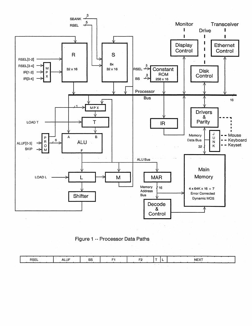
The microprocessor is shown schematically in Figures 'I and 2. A principal design goal in this system was to achieve the simplest structure adequate for the required tasks. As a result, the central portion of the processor contains very little application-specific logic, and no specialized data paths. The entire system is synchronous, with a clock interval of approximately 170 nsec. All microinstructions require one -cycle for their execution.
A second design goal was to minimize the amount of hardware in the liD controllers. This is achieved by doing most of the processing associated with 110 transfers with microprograms. To allow devices to proceed in parallel with each other and with CPU activity, a control structure was devised which allows the microprocessor to be shared among up to 16 fixed priority tasks. Switching among tasks requires very little overhead, and occurs typically every few microseconds.
2.1 Arithmetic Section
The arithmetic section of the processor consists of two 32-word by 16-bit register files Rand S, and five registers, T, L, M, MAR, and IR, The registers are connected to the memory and to an ALU with a 16-bit parallel bus. For historical reasons, the sand M registers are viewed as part of the microinstruction RAM and are described in section 8.
The ALU is a sl\'74181 type, restricted so that it can do only 16 arithmetic and logical functions. The ALU output feeds the L, M, and MAR registers. T may also be loaded from the ALU output under certain conditions. L is connected to a shifter capable of left and right shifts by one place, and cycles of 8. It has a mode in which it does the peculiar 17-bit shifts of the standard instruction set, and a mode which allows double-length shifts to be done.
The IR register is used by the emulator to hold the current emulated instruction -- see section 3.5.
Attached to the bus is a 256-word read only memory (ROM) which holds arbitrary 16-bit constants.
The fields of the 32-bit microinstruction are:
FIELD NAME MEANING
0-4 RSELECT R Register Select 5-8 ALUF ALU Function 9-11 BS Bus Data Source 12-15 Fl Function 1 16-19 F2 Function 2 20 T Load T 21 L Load L & M 22-31 NEXT Next microinstruction address (subject to modifiers)
When microprogramming the Alto, it is important to understand where the machine's state resides and how it changes. At the beginning of a microinstruction cycle, the various registers (principally T, L, M, and IR, but also various bits of state such as ALUCO) contain values that remain unchanged throughout execution of the microinstruction. During this time, the various non-state-retaining data paths and elements, such as the bus, ALU, and shifter, compute results based entirely on the initial values of these
RSEL[O·2] ---~ .... ~ ~
RSEL[3·4] ~ M
IR[1·2] . ~ P I--~
IR[3.4] ~ x ---
LOADT
r--P I--
ALUF[O·3] ~ R 6
0 SKIP ~ M ---
LOADL
3 SBANK ---,
L RSEL -.-
t
R S 4 ~ 8x
32x 16 32x 16
" " L t ~
j 1 .. MPX I
t I ..... T I
I t A B
ALU
F
,
I .... .1 L M I
I
Shifter I
5 RSEL -4 Constant
3 ROM BS -4 256 x 16
Processor , .
Bus
, IR
- ALU Bus
MAR
Memory Address Bus II
16
Decode &
Control
Figure 1 -- Processor Data Paths
Monitor Transceiver I Drive I I I I
I Display Ethernet Control I Control·
I I' f'
I
Disk Control
f'
I II W ,
I' 16
\11
Drivers & --- ..
Parity • • I~ • - •
Memory J - - Mous e Data Bus I--
U - - Keybo ard N
32 K
,It -
Main Memory
4x64Kx 16 + 7 Error Corrected
DynamicMOS
t
- - Keyse t

Alto Hardware Manual Section 2: Microprocessor 4
registers. However, the registers themselves do not change.
At the end of the cycle, if the microinstruction specifies that one or more registers be loaded, they are loaded instantaneously and simultaneously with the newly-computed values. These then serve as the initial register values for the next microinstruction. As a result, it is possible (and in fact very common) to both read and load a register during the same microinstruction. The R registers behave similarly except that it is not possible to both read and load an R register during the same microinstruction.
R SELECT
The R select field specifies one of the 32 R cells to be loaded or read under control of the bus source field,or, in conjunction with the bus source field, one of the 256 locations to be read from the constant· ROM. The R field is also used to address registers in S -- see section 8.
The low order two bits of the R address (but not the constant ROM address) may be taken from fields in IR under control of the functions. This allows the emulator to address its central registers easily.
ALU FUNCTIONS
The ALUF field controls the sN74181 ALU. This device can do a total of 48 arithmetic and logical operations, most of which are relatively useless. The 4-bit field is mapped by a PROM into the 16 most useful functions.
ALUF T FUNCTION S3 S2 Sl SO M C OPERA.TION
0 * BUS 1 1 1 1 1 0 A 1 T 1 0 1 0 1 0 B 2 * BUS OR T 1 1 1 0 1 0 A+B 3 BUS AND T 1 0 1 1 1 0 AB 4 BUS XOR T 0 1 1 0 1 0 AXORB 5 * BUS + 1 0 0 0 0 0 0 A PLUS 1 6 * BUS -1 1 1 1 1 0 1 A MINUS 1 7 BUS + T 1 0 0 1 0 1 A PLUS B lOB BUS - T 0 1 1 0 0 0 A MINUS B llB BUS - T - 1 0 1 1 0 0 1 A MINUS B MINUS 1 12B * BUS + T + 1 1 0 0 1 0 0 A PLUS B PLUS 1 l3B * BUS + SKIP 0 0 0 0 0 SKIP A PLUS 1 14B * BUS. T (AND) 1 0 1 1 1 0 AB 15B BUS AND NOTT 0 1 1 1 1 0 A & NOT B 16B-17B UNDEFINED
If T is loaded in an instruction containing an ALUF with a * in the T column, it will be loaded from the ALU output rather than from BUS.
S3-S0 selects the function; M selects logical or arithmetic mode by controlling carry propagation; C is the carry into the LSB. The carry output is forced to zero during logical operations (M = 0). input to the ALU; T is the B input.
BUS SOURCES
The bus data source (BS) field
BS NAME
o <-RName 1 RName<-2 (None) 3 Task-specific
specifies one of 8 data sources for the bus:
SOURCE
Read R Load R from shifter output (see below) Enables no source to the BUS, leaving it all ones Performs different functions in different tasks.
BUS is the A

Alto Hardware Manual
4 5 6 7
Task-specific "'MD ... MOUSE "'DISP
Section 2: Microprocessor
Performs different functions in different tasks. Memory data Bus[12-15]+- MOUSE; BUS[O-13]+- -1 IR[8-15], possibly sign extended (see section 3.5)
5
RName+- is not logically a source, but because it is gated to the bus during both reading "and writing, it is included in the source specifiers. Loading R forces the BUS to 0 so that an ALU function of 0 and T may be executed simultaneously.
The bus has the property that if more than one source is gated to it during a single microinstruction, it computes the AND of the source values. This is true regardless of the means by which the sources are enabled (BS, Fl, or F2).
This bus source decoding is not performed if Fl=7 or F2=7. These functions use the BS field to provide part of the address to the constant ROM.
SPECIAL FUNCTIONS
The two function fields specify the address modifiers, register load signals (other than those for R, S, L, M and T), and other special conditions required in the processor. The first eight conditions specified by each field (except BLOCK) are interpreted identically by all tasks, but the interpretation of the second eight depends on the active task. The task-independent functions are given below; the task-specific functions are included with the task descriptions.
FUNCTION 1:
Fl o 1
2 3
4 5 6 7
NAME
MAR'"
TASK BLOCK
"'L LSH 1
"'L RSH 1
"'L LCY8 "'CONSTANT
MEANING No Activity Load MAR from ALU output; start main memory reference (see section 2.3). Switch tasks if higher priority wakeup is pending (see section 2.4). Disable the current task until re-enabled by a hardware-generated condition. Note: this function is reserved by convention only; it is not done by the microprocessor. SHIFTER OUTPUT will be L shifted left one place* SHIFTER OUTPUT will be L shifted right one place* SHIFTER OUTPUT will be L rotated left 8 places* Put on the bus the constant from the constant ROM location addressed by RSELECT.BS
*Modified by DNS (DO Novel Shifts) function, and MAGIC function. L LSH land L RSH 1 ordinarily shift a zero into the vacated bit position.
FUNCTION 2:
F2 NAME MEANING 0 No Activity 1 BUS=O NEXT'" NEXT OR (if (BUS=O) then 1 else 0). 2 SH(O NEXT'" NEXT OR (if (SHIFTER OUTPUT(O) then 1 else 0).* 3 SH=O NEXT'" NEXT OR (if (SHIFTER OutPUT=O) then 1 else 0).* 4 BUS NEXT'" NEXT OR Bus[6-15]

Alto Hardware Manual Section 2: Microprocessor 6
5
6 7
ALUCY
MD<<-CONSTANT
NEXT<- NEXT OR ALUco. ALUCO is the carry produced by the ALU during the most recent microinstruction that loaded L. It is not the carry produced during execution of the microinstruction that contains the ALUCY function. Deliver BUS data to memory (see section 2.3) Same as Fl=7
*Note that the value of the SHIFTER Ourpur is determined by the value of L as the microinstruction begins execution and the shifter function (L LSH 1, L RSH 1, or L LCY 8) specified during the current microinstruction (if no shifter function is specified, the shifter output is equal to L).
2.2 Constant Memory
The constant memory is a 256 x 16 PROM that holds arbitrary constants. The constant memory is gated to the bus by Fl=7, F2=7, or BS>4. The constant memory is addressed by the (8 bit) concatenation of RSELECT and BS. The intent in enabling constants with Bs>4 is to provide a masking facility, particularly for the <-MOUSE and <-DISP bus sources. This works because the processor bus ANDS if more than one source is gated to it. Up to 32 such mask constants can be provided for each of the four bus sources >4.
Alto I: Note that it is not possible to use a constant other than -1 with the +- MD bus source, because memory parity is calculated on the bus, and a parity error will result if bits are masked off in a word fetched from memory.
2.3 Main Memory
Main memory references are handled differently on Alto I and Alto II. It is, however, possible to write most microcode so that it will operate correctly on both machines.
BASICS
Memory is addressed by a 16-bit number that refers to a 16-bit word in the memory. Addresses 0 through 176777B are true memory storage locations; addresses 177000B through 177777B are used to control 1/0 devices that are attached to the Alto memory bus. Some operations on memory are performed on "double-words." The double-word beginning at location adr (adr is even) is a 32-bit quantity equivalent to the 16-bit contents of location adr, together with the 16-bit contents of location adr+ 1. (Double-word references operate correctly only on true memory locations, not on I/O device locations.)
MEMORY REFERENCES
Alto I and Alto II: A memory reference is initiated by executing Fl = 1, MAR <-. The results of a read operation are delivered somewhat later onto the bus with BS = 5, "MD. A store into the addressed memory location is achieved with F2=6, MD<-. The microprogram partially controls memory timing, and must observe certain rules to insure correct operation.
a) A minimum of one microinstruction must intervene between the initiation of a memory reference and an MD<- or <-MD.
b) On both Alto I and Alto II, memory cycles last a total of 5 micro-cycles, although doubleword operations may extend the memory cycle to take a total of 6 micro-cycles. Although the exact details of memory timing differ on Alto I and Alto II, both machines share the property that the processor will suspend execution of microinstructions if the memory

Alto Hardware Manual Section 2: Microprocessor 7
interface cannot process the function (MAR <-, MD<- or <- MD) specified; processing will resume as soon as the interface is free. It is permissible to "abandon" a memory reference that has already been started simply by not referencing MD within the first 5 cycles, or by starting a new memory reference with MAR ~ .
c) The memory checks parity on all fetches, unless the cycle is a refresh cycle or the address is between 177000B and 177777B inclusive, in which case an I/O device is being referenced. Parity errors result in activation of a high-priority task (task number 15B) whose purpose is to deal with the error (see section 5.5). The Alto II checks memory parity on store as well as fetch cycles.
d) If RSELECT = 37B during the instruction which starts the memory, a refresh cycle is assumed and all memory cards are activated. . This is used by the refresh task.
e) MAR<- cannot be invoked in the same instruction as <-MD of a previous access.
In the discussion that follows, we assume that a memory reference has been started with MAR <-, and we designate this instruction (micro)cycle 1. Examples of proper sequences are given below.
Alto I
Alto II
f) During cycle 5, if F2=6,. MD<-, a store of bus data into the word addressed by MAR will occur. The MD<- may not be issued later than cycle 5. (Note: Some Alto 1's have been modified to allow a "double-word store." On these machines, it is permissible to issue two MD<- instructions in a row, the first coming in cycle 5, and the second in cycle 6. If MAR is loaded with an even address adr, the two words will be stored at adr and adr+ 1 respectively.)
g) During cycle 5 of a reference, if BS = 5, <- MD, the reference is a fetch of the word addressed by MAR. During cycle 6, if BS = 5, <- MD, the odd word of the doubleword addressed by MAR is delivered. If MD is referenced during cycle 6, it also must have been referenced (by either +-MD or MD+-) during cycle 5.
f) During cycle 4, if F2=6, MD<-, a store of bus data into the word addressed by MAR will occur. The MD<- may not be issued later than cycle 4. Alto II's allow a "double-word store:" it is permissible to issue two MD<- instructions in a row, the first coming in cycle 3, and the second in cycle 4. If MAR is loaded with an address adr, the two words will be stored at adr and (adr XOR 1) respectively.
g) During cycle 5, if Bs=5, <-MD, the reference is a fetch of the word addressed by MAR. During cycle 6, if Bs=5, <-MD, the other word of the doubleword addressed by MAR is delivered. Again, if MAR is loaded with address adr, the two words fetched will be from location adr and (adr XOR 1) respectively.
h) Because the Alto II latches memory contents, it is possible to execute <- MD anytime after cycle 5 of a reference and obtain the results of the read operation.
EXAMPLES
Because the description above is a bit terse, we shall give several examples for Alto I operation, for Alto II operation, and for coding schemes that will work properly on both kinds of Altos. In the coding examples, REQUIRED stands for some microinstruction (you supply it) that must appear in the sequence; SUSPEND stands for a microinstruction which if omitted will cause execution to suspend for one cycle because the memory interface is not ready; OPTIONAL stands for a microinstruction which may be omitted without penalty. The notation ANY will be used to stand for an arbitrary 16-bit address; EVEN will stand for an even 16-bit address. All of these examples apply to extended memory references also (described in the next section); simply substitute XMAR for MAR.

Alto Hardware Manual
Simple
Simple
Simple
fetch:
Alto I
MAR+-ANY; REQUIRED; SUSPEND; SUSPEND; whereever+-MD;
store:
Alto I
MAR+-ANY; REQUIRED; SUSPEND; SUSPEND; MD+-whatever;
store, followed
Alto I
MAR+-ANY; REQUIRED; SUSPEND; SUSPEND; MD+-whatever; MAR+-ANY;
Double-word fetch:
Alto I
MAR+-EVEN; REQUIRED; SUSPEND; SUSPEND; whereever+-MD; whereever+-MD;
Alto II
MAR+-ANY; REQUIRED; SUSPEND; SUSPEND; whereever+-MD;
Alto II
MAR+-ANY; REQUIRED; OPTIONAL; MD+-whatever;
immediately by another
Alto II
MAR+-ANY; REQUIRED; REQUIRED; MD+-whatever; SUSPEND; MAR+-At-.'Y;
Alto II
MAR+-ANY; REQUIRED; $USPEND; SUSPEND; whereever+-MD; whereever+-MD;
Double-word store/fetch:
Alto I
MAR+-EVEN; REQUIRED; SUSPEND; SUSPEND; MD+-whatever; whereever+-MD;
Alto II
MAR+-ANY; REQUIRED; SUSPEND; MD+-whatever; whereever+-MD;
Double-word store (only on modified Alto Is):
Alto I Alto II
MAR+-EVEN; REQUIRED; SUSPEND;
MAR +- Al\'Y; REQUIRED; MD+-whatever;
Section 2: Microprocessor
memory cycle:
Alto II
MAR+-ANY; REQUIRED; MD+-whatever; SUSPEND; SUSPEND; MAR+-ANY;
8

Alto Hardware Manual
SUSPEND; MD+-whatever;
. MD+-whatever;
Section 2: Microprocessor
MD+-whatever;
The Alto II memory buffering permits a double-word "exchange":
MAR+-ANY; REQUIRED; MD+-newcontents1; MD+-newcontents2; L+-MD; T+-MD; 0idContents1 +-L, L+-T; 0ldContents2+-L;
address address address address
=. adr = adr XOR 1 = adr = adr XOR 1
Microcode which uses the memory timings below will work on either vintage of Alto:
Simple fetch: (as Alto I).
Simple store: (as Alto II). ««( Nota Bene
Double-word fetch: (as Alto I).
Double-word store/fetch: (as Alto II).
Others are not possible.
EXTENDED MEMORY
9
Main memory on Alto lIs can be optionally expanded to up to 256K words in 64K banks. Each task has associated with it four extra bank bits which are presented to the memory along with the 16 bit addresses generated by the task's microcode. Normal memory references are microcoded in the usual way and use two of the bank bits to specify the task's normal bank. Extended memory references are microcoded slightly differently and use the two other bank bits to specify the task's alternate bank. Thus a task can reference 64K very easily, another 64K with a little difficulty, and the other two 64K banks only after loading its bank registers appropriately.
To signal that a memory reference should go to the alternate bank, the microinstruction which loads MAR must also contain F2=6 (MD+-). The microassembler will generate this conbination of functions for a clause whose left hand side is XMAR (i.e., XMAR+- address will generate an instruction with Fl=l and F2=~ .
The bank registers appear as 16 words in the liD area which can be read and written. Location (177740B + N) is the bank register location for task N. Booting the Alto clears the registers to zeros making all references for all tasks go to bank zero, thus making the machine operate as a standard Alto without the extended memory option. Within a bank register, the layout is as follows:
BR[O-U] BR[12-13] BR[14-15] .
undefined normal reference bank number extended reference bank number
The highest 512 locations in each bank are not mapped by the bank registers and always refer to the 110 area. That means that location 177740B is the emulator's bank register regardless of what the referencing task's bank register contains and regardless of whether it is referenced with a normal or an extended memory reference.
No changes are necessary in order to run the display, disk, or Ethernet in different banks. The easiest and least confusing way to do this is to load the bank registers for all concerned tasks (e.g. DVT, DHT and DWT for the display, or KSEC and KWD for the disk) with some other bank number. Then the device is

Alto Hardware Manual Section 2: Microprocessor 10
controlled by the relevant words of page 1 in its bank.
Programs which use the extended memory must fIrst initialize it to have correct parity. This involves disabling parity interrupts, storing something in every word, flushing any parity interrupts that result, and then reenabling parity interrupts. The standard bootstrap loaders initialize bank zero only.
All Alto lIs manufactured starting with the 7th build have the extended memory option but are normally shipped with memory chips for bank zero only. Some earlier Alto lIs have been modifIed in the fIeld. Machines with the extended memory option have engineering number 3 -- see the description of the VERS instruction.
2.4 Microprocessor Control
Control of the Alto microprocessor is shared among 16 "tasks" arranged in a priority order. The tasks are numbered 0 to 15: 0 is the lowest priority task and 15 is the highest. The lowest priority task is the emulator task which fetches instructions and executes them.
The only state saved for each task is a "micro program counter," MPC. The current task number, saved in the current task register, addresses a 16 by 12 MPC RAM. The result is an MPC for the current task; it is used to address a lK by 32-bit read-only microinstruction memory (MI ROMO) or a 1K by 32-bit writeable microinstruction memory (MI RAMO), described in section 8. An optional feature of Alto lIs extends the MI ROM to 2K or the RAM to 3K -- see section 8.
BRANCHING
The microprocessor offers a limited branching capability which, although somewhat cumbersome, has proven adequate for chores undertaken by Alto microcode. The basic idea is that special microprocessor functions may. modify the NEXT fIeld, and consequently alter the flow Of control. Modification is accomplished by DRing various bits into the NEXT field.
Address modification is complicated slightly because the Alto pre-fetches one microinstruction ahead. Consequently, a branch condition modifies the NEXT field of the microinstruction following the one in which the condition test is placed. This property i~~ best" illustrated ... with an example:
MI location MI
100B 10lB 102B 103B
F2=2 (SH<O). NEXT=101B ... , NEXT = 102B
When the instruction at location 100B is being executed, the instruction at location 101B has already been fetched. Therefore, the SH<O test modifies the NEXT field of the on-deck instruction, the one at 10lB. Thus the two possible execution sequences are: (1) if L>O on entering the code above: 100B, 100B, 102B; (2) if L<O on entering the code: 100B, 10lB, 103B.
TASK SWITCHING
Only one of the 16 tasks is executing microinstructions at anyone time. Once a task begins execution, it continues to execute until it invokes a task switch function that enables switching to another task. A task is considered eligible for execution if its hardware-generated "wakeup signal" is asserted (these signals are not accessible to the microprogram). The wakeup signals enter a' priority encoder that calculates the number of the highest-priority eligible task. When a running task invokes a task switch, control will

W A S K I E G U N P A
L S
== == == :::::::::::::
=== == == ==
II
D E C 0 D E R
p R E
I N
0 C
R 0 I D
T E Iv R
C U R T
R A MPCRAM ... S 4 E 4
N K 16x12
T 2 ,10
I . Address
........ Modification /'
Logic
CRAM Address I
-, _J I MPX I
\It \
Address Address
Control Control Next Microinstruction
RAM ROM Address Bus
.... 1Kx32 ~ 1Kx32
or or 3Kx32 2Kx32
Data Out Data Out
I I I 10
22
il
I MIR I t
Instruction
Figure 2 -- Processor Control

Alto Hardware Manual Section 2: Microprocessor 11
switch to another task only if a higher priority task has a wakeup signal held true, or if the current task no longer has a wakeup signal true. In the latter case, control goes to a lower priority task. The lowest priority task is the CPU emulator, which is always requesting wakeup.
If the processor executes the TASK function (Fl=2) during an instruction, the current task register is loaded (at the end of the instruction) with the number of the highest priority task currently requesting a wakeup. This causes the next instruction to be fetched from the ROM location specified by the saved task's MPC. One additional instruction is executed by the current task before the switch becomes effective. This instruction may execute task-specific functions, but it must do no NEXT address modification, since· any such modification would affect the new task. The situation for two streams of instructions A-F and J-M in two different tasks is shown below:
Instruction Instruction Address stored in being executed being fetched MPC at end of cycle
A B C B C D C1 D E D J K J2 K L K3 L M L E F E F G
lInstruction C allows task switching. New task's MPC = J. 2Instruction J does an operation which removes its task's wakeup request. 3Instruciion K allows task switching, and the original task is now highest priority.
The BLOCK function (Fl=3) is used, by convention, to signal a hardware device associated with the currently running task to remove its wakeup signal. This function is not accomplished by the Alto microprocessor, but rather by the individual device interfaces.
Task switches must occur only at times when the current task has no state in any register (except R registers dedicated to the task) and has no main memory operation in progress, since there is no provision in the hardware for saving this information. That is, all state important to the task must have been stored in safe places by the end of the microinstruction after the one containing the TASK function. It is not legal to place TASK functions in two consecutive microinstructions.
INITIALIZATION
The only way in which the microprogram can affect the task structure is to request a task switch. In particular, it cannot affect the MPCS of tasks other than itself. This presents an initialization problem which is solved by having each task start at the location which is its task number (thus the emulator task finds its first instruction to execute at MPC = 0). Task numbers are written into the MPC RAM during a reset cycle, which may be initiated manually or by a CPU instruction (see SID instruction in section 3.3). Tasks ordinarily begin execution in ROMO. In order to start tasks in the RAM, there is a mechanism for modifying the initial MPC'S of tasks so that they will begin execution in RAMO (see section 8.4)
STANDARD TASKS
The standard Alto and its associated device controllers use many of the available tasks. Detailed descriptions of the operation of most tasks· are found in the sections of this manual relevant to the hardware devices. Appendix D is a list of the standard tasks.

Alto Hardwa.re Manual Section 3: Emulator 12
3.0 EMULATOR
The lowest-priority Alto task is called the Emulator task. This task is always requesting wakeup, but can be interrupted by a wakeup request from any other task. In effect, the emulator task is the "background job." The standard Alto microcode ROM includes standard emulator task microcode for fetching from Alto memory, decoding,· and interpreting instructions from the Standard Instruction Set. In the rest of this chapter we shall frequently use the term "emulator" to mean "standard emulator task microcode." This standard microcode can be extended or replaced, usually by executing special emulator task microcode in the microinstruction RAM.
This section describes microcode versions installed after June 1976. To determine the vintage of a machine's microcode, see descriptions of SIO and VERS (section 3.2).
3.1 Standard Instruction Set
REGISTERS
The emulator state is carried from instruction to instruction in several registers:
PC: The "program counter," which contains the 16-bit address of the next instruction to be fetched and executed. It is actually implemented as R -register 6.
ACO, ACl, AC2, Ac3: The accumulators, each of which contains 16 bits. Instructions are available for transferring contents of accumulators to and from memory registers and for performing arithmetic and logical operations among accumulators. The notation AC(n) is often used to refer to the contents of accumulator n (n= 0,1,2,3). These accumulators are implemented as R -registers 3-0 respectively.
C: The "carry" bit which is modified by most arithmetic operations. It is implemented as special hardware (see section 3.5).
MEMORY: The Alto has "64K" 16-bit memory words, addressed by values ranging from 0 to 176777B. Addresses 177000B to 177777B are reserved for various I/O device uses (see Appendix B). Memory on Alto IIs can be extended to 256K in 64K banks (see Section 2.3).
Additional R - and S-registers may be used temporarily during emulation of a single instruction.
INSTRUCTION FORMAT
The standard instruction set is best described by breaking it into four groups according to the way the instructions are formatted (see Figure 3).
Several of the instructions compute an "effective address" based on the values of the I (indirect), X (index) and DISP (displacement) fields of the M-group, J-group and some s-group instructions. The effective address calculation is best described by a brief "program." First we define the function SignExtend(x) to represent the sign-extension of the 8-bit number x:
SignExtend(x) = if x > 200B then x+177400B else x.
Then EffAddrO, the function to compute the effective address is:

o I) 2
o I MFunc I DestAC I I x
M-Group LDA (MFunc = 1)
ST A (MFunc = 2)
o IJFUnC I I X
J-Group JMP (JFunc = 0)
JSR (JFunc = 1) ISZ (JFunc = 2)
DSZ (JFunc = 3)
1 I SrcAC I DestAC I AFunc A-Group
1 1
S-Group
COM (AFunc = 0) NEG (AFunc = 1)
MOV (AFunc = 2)
INC (AFunc = 3)
ADC (AFunc = 4) SUB (AFunc = 5)
ADD (AFunc = 6)
AND (AFunc = 7)
AugmentedFunc
8 )) 12 113
DISP
x = 0: Page 0 addressing
X = 1: PC-relative addressing
X= 2: Base-register (AC2)
X = 3: Base-register (AC3)
DISP
14
SH CY INL I . SK
L(SH= 1) R (SH=2)
S (SH=3)
Z(CY=1) O(CY=2)
C(CY=3)
DISP·
--# (NL=1) SKP(SK=1)
SZC(SK=2)
SNC(SK=3) SZR (SK=4)
SNR(SK=5) SEZ(SK=6)
SBN(SK=7)
Figure 3 -- Instruction Formats

Alto Hardware Manual
EffAddrO = [ E+- (
if elseif elseif elseif )
Section 3: Emulator
liThe symbol "E"denotes effective address I IValues of I,X, and DISP are from the instruction
x = 0 then DISP x=l then SignExtend(DIsP)+PC x = 2 then SignExtend(DIsP) + AC(2) x=3 then SignExtend(DIsP)+AC(3)
I/"page 0 addressing" I I"relative addressing" I /"base register addressing" I /"base register addressing"
13
if I ;t: a then E+-rv(E) ].
IINow do single-level indirection
The notation for these addressing modes is demonstrated below. The DISP value is always specified first; . the x value is not given explicitly, but is determined either by the address of the label or by a modifier ",2" or ",3" which specifies base register indexing:
JMP LABEL2 JMP 15,3 JMP @3
; If LABEL2 is in page 0, X=O; otherwise X=l. ; OISP=15; 3 means use AC3 as base register. ; The character @ causes I to be 1.
Note that instructions which compute an effective address always do so before any other operations. Thus JSR 1,3 computes the effective address of 1 + Ac(3) before saving PC+ 1 in AC3.
MEMORY GROUP OPERATIONS
The DestA.C field specifies one of the four accumulators (DestA.C = a for ACO, DestAC = 1 for Ac1, etc.). The MFunc field specifies one of two operations:
Mnemonic MFunc Action
LDA STA
1 2
This operation loads an accumulator from memory. This operation stores an accumulator into memory.
AC(DeStAc)+-rv(E). rv(E)+-AC(DeStAc).
These instructions are written by giving the mnemonic, followed by the accumulator number (DeStAC), followed by an effective address notation:
STA 3 .+4 LOA 0 4,2 LOA 0 @.+2
Store AC3 in the fourth location following here Load ACO from address=4+AC(2) Load ACO from address contained in second location following here
JUMP AND MODIFY GROUP OPERATIONS
The JFunC field specifies one of four operations:
Mnemonic JFunc
1MP a JSR 1
ISZ 2
DSZ 3
Action
This operation causes a "jump" by changing the value of the PC. PC+-E. This operation is useful when calling subroutines because it saves a return address in Ac3. AC(3)+-pc+1; PC+-E. This operation increments the contents of a memory cell and skips if the new contents are zero. rv(E)+-rv(E)+ 1; if rv(E) = 0 then PC+-PC+ 1. This instruction does not alter the C bit. This instruction decrements the contents of a memory cell and skips if the new contents are zero. rv(E)+-rv(E)-l; if rv(E) = 0 then PC+-PC+1. This instruction does not alter the C bit.

Alto Hardware Manual Section 3: Emulator 14
These instructions are written by giving the mnemonic and the effective address notation:
JSR SUBR JMP 1,3
AC3 is left pOinting to the location after this one Jump to AC(3)+1
ARITHMEfIC GROUP OPERATIONS
All 8 of these instructions operate on the contents of the accumulators and the carry bit. Typically, a binary operation involves the contents of the "source accumulator" (srcAc) and the "destination accumulator" (DeStAc) and leaves the result in the destination accumulator. The carry bit (c bit) and the PC can also be modified in the process.
The operation of the instructions is best explained by following the flow in Figure 4. The 16-bit contents of the source and destination accumulators are fetched and passed to the function generator.
The carry generator produces an output that depends on the value of the C bit and the CY field of the instruction:
Mnemonic CY Output
none 0 C Z 1 0 0 2 1 C 3 l-C (Le., the complement of c).
The function generator is controlled by the AFUnc field; various values will be described below. It takes two 16-bit numbers and a carry input and generates a 16-bit Result and a carryResult.
The shifter is controlled by the SH field in the instruction:
Mnemonic SH
none 0 L 1
R 2
S 3
Action
No shifting; the 17 output bits are the same as the 17 input bits. Rotate the 17 input bits left by one bit. This has the effect of rotating bit o left into the carry position and the carry bit into bit 15. Rotate the 17 bits right by one bit. Bit 15 is rotated into the carry position and the carry bit into bit O. Swap the 8-bit halves of the 16-bit result. The carry is not affected.
The skip sensor tests various of the 17 bits presented to it and may cause a skip (pc+-PC+ 1) if an appropriate condition is detected:
Mnemonic SK
none 0 SKP 1 SZC 2 SNC 3 SZR 4 SNR 5 SEZ 6 SBN 7
Action
Never skip Always skip Skip if the carryResult is zero Skip if the carryResult is non-zero Skip if the 16-bit Result is zero Skip if the 16-bit Result is non-zero Skip if either carryResult or Result is zero Skip if both carryResult and Result are non-zero
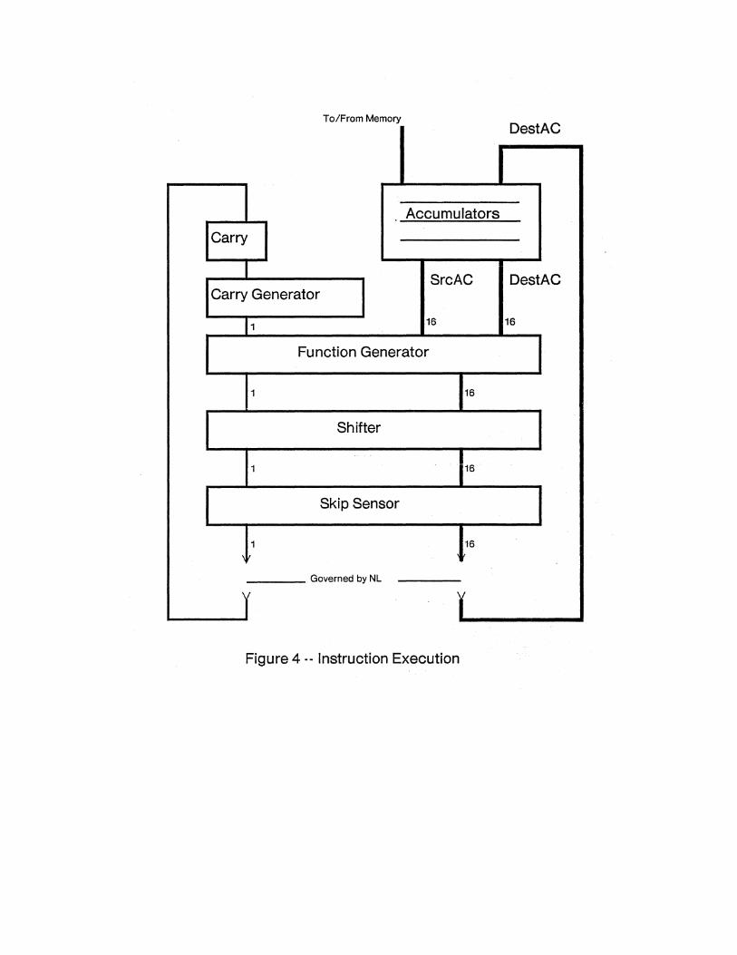
To/From Memory D tAC es
Accumulators
Carry
SrcAC DestAC Carry Generator
1 16 16
Function Generator
1 16
Shifter
1 16
Skip Sensor
1 16
Governed by NL
Y I Figure 4 ee Instruction Execution

Alto Hardware Manual Section 3: Emulator 15
The alert reader will detect that the SK field is microcoded. The skip condition can be described as:
skip = (SK[2):;e0) XOR «SK[O):;eO AND result = 0) OR (sK[l):;eO AND carryResult= 0))
where SK[O) is the first bit of the field, SK[1] the second and SK[2]the third.
The NL bit in the instruction controls the operation of the switch in the illustration. If NL= 1, neither the destination accumulator nor the carry bit is loaded; otherwise the destination accumulator is loaded from Result and the carry bit from carryResult The "no-load" feature is useful for instructions whose only use is testing some value. The character # is appended to the mnemonic for operations if the NL bit is to be set
The AFUnc operations are described below. Note that "Result" will be stored into the destination accumulator (DeStAc) unless NL=l.
Mnemonic AFUnc Operation Description
COM
NEG
MOV
INC
ADC
SUB
ADD
AND
o
1
2
3
4
5
6
7
COMPLEMENT The function generator produces the logical complement of Ac(srcAc). It passes the carry bit unaffected.
NEGATE The function generator produces the two's complement of Ac(srcAc). If Ac(srcAc) contains zero, complement the value of the carry supplied to the function generator, otherwise supply the specified value.
MOVE The function generator passes Ac(srcAc) and the carry bit unaffected.
INCREMENT The Result produced ·.is AC(SrcAC) + 1; the carry is complemented if Ac(srcAc) = 177777B.
ADD COMPLEMENT The Result produced is the sum of AC(DeStAc) and the logical complement of AC(SfCAC). The carry bit is complemented if the addition generates a carry.
SUBTRACT Subtracts by adding the two's complement of Ac(srcAc) to AC(DeStAc). The carry bit is complemented if the addition generates a carry ..
ADD Adds Ac(srcAC) to AC(DestAc). The carry bit is complemented if the addition generates a carry.
AND The Result is the logical and of Ac(srcAC) and AC(DeStAc). The carry is passed unaffected.
The arithmetic instructions are written by citing. the AFUnc mnemonic, followed optionally by the CY mnemonic, followed optionally by the SH mnemonic, followed optionally by the NL mnemonic. Then after a space, the source accumulator number is given, the destination accumulator number, and optionally an SK mnemonic. For example:
SUB 0 0 MOVZ 2 1 SUBZL 1 1 ADC 0 0 SUB# 2 3 SNR
COM# 1 1 SZR SUBZ# 1 0 SZC ADCZ# 1 0 SZC
Zero ACO by subtracting it from itself Move AC2 to AC1, and zero C Set AC1 to 1 Set ACO to 177777B Skips if AC2 and AC3 are unequal but affects neither Skips if AC1 is 177777B but leaves it unchanged Skips if ACO(AC1 unsigned. Skips if ACOiAC1 unsigned
To subtract the constant 1 from Ac1:

Alto Hardware Manual Section 3: Emulator
NEG 1 1 COM 1 1
To OR together the contents of ACO and Ac1; result in ACO:
COM 1 1 AND 1 0 ADC 1 0
To XOR together the contents of ACO and- Ac1; result in ACO:
MOV 0 2 ANDZL 1 2 ADD 1 0 SUB 2 0
To negate a double-length number in ACO and Ac1:
NEG 1 1 SNR NEG 0 0 SKP COM 0 0
To add the double-length number in Ac2,AC3 to one in ACO,AC1:
ADDZ 3 1 SZC INC 2 2 ADD 2 0
To subtract the double-length number in Ac2,AC3 from one in ACO,AC1:
SUBZ 3 1 SZC SUB 2 0 SKP ADC 2 0
16
The Bcpl construct "if a gr b then ..... uses code which does a subtract and checks the sign. Unfortunately, this is not a true signed compare because the subtract may overflow. With this code, 2 gr 0 is true, but 077777B gr 100000B is false (077777B is the largest positive number and 100000B the largest negative). The code generated by Bcpl looks like:
LDA 0 4,2 LDA 1 5,2 ADCL# 1 0 SZC JMP falsePart JMP truePart
Pick up a Pick up b Subtract and check sign Not true True
The "true signed compare" for vb is:
LDA 0 4,2 LDA 1 5,2 SUBZR 2 2 AND 1 2 ADDL 0 2 ADC# 1 0 SNC JMP falsePart JMP truePart
S-GROUP INSTRUCTIONS
Pick up a Pick up b Place 100000B in AC2 AC2=(if b<O then 100000B else 0) CARRY=(if a and b signs differ then 1 else 0)
Opcodes in the range 60000B-77777B, are assigned to the s-group, which comprises a variety of miscellaneous instructions and unimplemented operations. Bits 3 through 7 of the instruction determine 32 opcodes, each of which may use the displacement field (bits 8-15 of the instruction). One of these opcodes (61xxx, O<xxx::S;377B) uses the displacement field to represent up to 256 instructions which do not require a displacement or a parameter as part of the opcode.

Alto Hardware Manual Section 3: Emulator 17
Currently, only a small number of the available s-group instructions have been implemented. The remaining unimplemented instructions all trap in one of two ways:
ROM trap PC is saved in location TRAPPC, and then a JMP@ TRAPVEC+OP instruction is simulated. OP is bits 3-7 of the trapping instruction.
TRAPPC 527B
TRAPVEC 530B-567B
When an unimplemented opcode is executed by the emulator, the PC is saved here. It points to the location after the trapping instruction.
Contains pointers to the trap routines for the 32 opcodes (bits 3-7 of· the . trapping instruction). The first word corresponds to opcode 6Oxxx, O<xxx<377B.
RAM trap If no microinstruction RAM is present, the trap is handled as a ROM trap. If a RAM is present, the microcode transfers to location TRAPl in the RAM with the trapping instruction in L, the instruction cycled by 8 bits in the R-register XREG, and PC pointing to the location after the trapping instruction.
This arrangement makes it convenient to extend the Alto's standard instruction set by implementing additional functions in software which is dispatched to via TRAPVEC, or in microcode which is dispatched to via a RAM trap. An appendix tabulates the s-group instruction set opcodes and what each does or how it traps.
MUL
DIV
CYCLE
JSRII
JSRlS
61020B Unsigned multiply:
Multiply the unsigned integers in Ac1 and Ac2 to generate-a- 32-bit product; add the product to the integer in ACO. Leave the high-order part of the result in ACO and the low-order part in ACl. Ac2 is unaffected.
61021B Unsigned divide:
The double-length unsigned integer in ACO and Ac1 is divided by the unsigned integer in Ac2. The quotient is left in Ac1; the remainder in ACO. Ac2 is unaffected. The instruction normally skips the next instruction; if overflow occurs (ACO > Ac2 unsigned), DIV does not skip.
60000B Left cycle ACO:
Left cycle (rotate) the contents of ACO by the amount specified in instruction bits 12-15, unless this value is zero, in which case cycle ACO left by the amount specified in bits 12-15 of Acl.
64400B Jump to subroutine double indirect, PC relative:
AC3+-PC+l PC+- rv(rv(pc+ SignExtend(DIsP»)
65000B Jump to subroutine double indirect, AC2 relative:
AC3+-PC+l PC+-rv(rv(AC2+ SignExtend(DISP»)
Alto Hardware Manual Section 3: Emulator 18
CONVERT 67000B Scan convert a font character:
The CONVERT instruction does scan conversion of characters, i.e., it transfers data between an area of main memory containing a font and an area of memory containing a bit map to be displayed on the TV monitor.
CONVERT takes a number of arguments:
ACO contains the address of the destination' word into which the upper left corner of the character is to be placed, offset by NWRDS, the number of words to be displayed on each scan line (ACO=DWA-NWRDS).
Ac3 points to a character pointer in the font for the character to be displayed (Ac3 = FONTBASE + CHARACTER CODE).
Ac2+SignExtend(DISP) is the address of a two-word table:
word 0:
word 1:
NWRDS (number of words per to scan line); NWRDS < 128.
DBA, the destination bit address corresponding to the left hand edge of the character. CONVERT interprets this bit address reversed from the normal convention, i.e., 0 is the least significant bit, 15 the most significant bit.
CONVERT requires that a 16 word mask table be set up starting at MASKTAB (460B) in page l. rv(MAsKTAB+n)= (21'(n + 1»-1 (~ns...15).
The format of an Alto font designed for use with CONVERT is given below; names of font files in this format conventionally have an extension ".AL". The CONVERT instruction does not examine the words at FONTBASE-2 and FONTBASE-l; these are provided solely for convenience of software.
FONTBASE-2:
The height of a line of text in scan lines. This number incorporates the effects of the highest and lowest character in the font, i.e. it is max(HD+xH)-min(HD) where the max and min are taken independently and HD and XH are defined below.
FONTBASE-l:
Bit 0: 0 = Fixed width font. 1 = Proportional width font.
Bits 1-7: Baseline -- number of scan-lines from top of highest character in font to the baseline.
Bits 8-15: The width of the widest character in raster points.
FONTBASE to FONTBASE+ 377B:
Self-relative pointers to word xw of the character descriptor block for the character codes 0-377B.
FONTBASE+400B to FONTBASE+400B+EXTCNT-l:
These locations contain self-relative pointers to word xw of the character descriptor blocks for extensions, i.e., portions of characters which are wider than 16 bits. EXTCNT is the total number of character extensions.
Alto Hardware Manual Section 3: Emulator 19
RCLK
SIO
FONTBASE+400B+ EXTCNT to end:
Contains a number of character descriptor blocks of the form:
word 0 to word xw-I: The bit map for the character and surrounding spaces. The bit map does not include O's at the top and bottom of the character, as the character will be vertically positioned by CONVERT. The upper left-hand bit of the character is in the MSB of word O.
word xw: If the character is ~ 16 bits wide, this word contains (2*width)+1. If the character is > 16 bits wide, this word contains 2* a pseudo-character which is used as a character code to index an extension character in the font. If this is the last extension block of a character, this word contains (2* the width of the fmal extension), rather than the total width. The pointer indexed by the character code points to this word.
word xw+I: In the left byte, HD. In the right byte, XH. HD is the number of scan lines to skip before displaying the character, XH is the height of the bit map for this character.
The CONVERT instruction ORS the character bitmap into the display area. If the character does not require an extension, CONVERT skips, with the following information in the AC'S:
ACO: unchanged ACI: DBA AND 17B Ac2: unchanged Ac3: the width of the character in bits
If the character requires an extension, CONVERT returns does not skip. Ac3 contains the pseudocharacter code for the extension, and AC'S 0-2 are as above.
6I003B Read Clock:
The microcode maintains a 26 bit real time clock which is incremented by the memory refresh task at 38.08 microsecond intervals (more precisely, once every 224 ticks of the system clock, whose nominal frequency is 5.880000 MHz). The high-order 16 bits of this clock are maintained in location RTC (430B) in page 1 The low-order 10 bits are kept in R37. The remaining 6 bits of R37 contain state information unrelated to the time. RCLK loads ACO with the contents of location RTC, and loads AcI with the contents of R37. The period of the full 26-bit clock is about 40 minutes.
The contents of R37 are slightly different on Alto I and Alto II: on Alto I, R37[0-9] contain. the low order clock bits; on Alto II, R37[4-13] are used. Consequently, on the Alto I, the contents of ACO and AcI returned by RCLK may be viewed as a 32-bit clock in units of .595 microseconds, provided AcI[IO-I5] is first zeroed.
61004B Start 110:
Start I/O is included to facilitate 110 control. It places the contents of ACO on the processor bus and executes the STARTF function (Fl= 17B). By convention, bits of ACO must be "1" in order to signal . devices. See Appendix C for a· summary of assigned bits.

Alto Hardware Manual Section 3: Emulator 20
BLT
BLKS
SIT
If bit 0 of ACO is 1, and if an Ethernet board is plugged into the Alto, the machine will boot, just as if the "boot button" were pressed (see sections 3.4, S.4, and 9.2.2 for discussions of bootstrapping).
SIO also returns a result in ACO. If the Ethernet hardware is installed, the serial number and/or Ethernet host address of the machine (0-377B) is loaded into AcO[S-lS]. (On Alto I, the serial number and Ethernet host address are equivalent; on Alto II, the value loaded into ACO is the Ethernet host address only.) If Ethernet hardware is missing, AcO[S-lS] = 377B. Microcode installed after June 1976, which this manual describes, returns ACO[O]=O. Microcode installed prior to June 1976 returns ACO[O] = 1; this is a quick way to acquire the approximate vintage of a machine's microcode. .
6100SB
61006B
Block transfer:
Block store:
These instructions use tight microcode loops to move a block of memory from one place to another (BLT) or to store a constant value into a block of memory (BLKS). Block transfer and block store take the following arguments:
ACO: Address of the first source word-1 (BLT), or data to be stored (BLKS). Ac1: Address of the last word of the destination area. Ac3: Negative word count.
Because these instructions are potentially time consuming, and keep their state in the AC'S, they are interruptable. If an interrupt occurs, the PC is decremented by one, and the AC'S contain the intermediate state. On return, the instruction continues. On completion, the AC'S are:
ACO: Address of last source word + 1 (BLT), or unchanged (BLKS). Ac1: Unchanged. Ac2: Unchanged. Ac3: O.
The first word of the destination area (Ac1 + Ac3 + 1) is the first to be stored into.
61007B Start interval timer:
The microcode implements an interval timer which has a resolution of 3S.0S microseconds, and a maximum period of 10 bits. Because the principal application for this timer is to do bit sampling for a serial EIA-RS232 compatible communications line, the timer is specialized for this purpose. It uses three dedicated locations in page 1:
ITTIME S2SB Contains the time at which the next timer interrupt should be caused. On
mBITS
ITQUAN
Alto I, the lO-bit time is stored in ITTIME[0-9], and the remaining bits must be zero. On Alto II, the time is stored in ITTIME[4-13], and the remaining bits must be zero.
423B This word contains one or more bits specifying the channel or channels on which the timer interrupt is to occur.
422B When the interval timer interrupt is caused, the microcode stores a quantity in this location which depends on the mode.
The SIT instruction ORS the contents of ACO into R37. The high 14 bits should be 0; the loworder 2 bits determine the interval timer mode:

Alto Hardware Manual Section 3: Emulator 21
R37[14-1S]
o Off.
1 Normal mode. Every 38.08 microseconds, test to see if (R37 AND TIMEMASK)=ITIIME (on Alto I, TIMEMASK=177700B; on Alto II, the proper value for TIMEMASK is 7774B, but version 23 of Alto II microcode uses a value of 7700B). If they are equal, cause an interrupt on the channel specified by ITIBITS. Store the current state of the EIA interface in ITQUAN, and set R37[14-1S] to zero. The state of the EIA interface is bit IS of location EIALOC (17770lB) in page 377B. This bit is 0 if the line is spacing, 1 if it is marking.
2 Same as O.
3 Every 38.08 microseconds, check the state of the. EIA line by reading EIALOC. If the line is marking (EIALOC is non zero), do nothing. If the line is spacing, cause an interrupt on the channel specified by ITIBITS. Store the current value of R37 in ITQUAN, and set R37[14-1S] to zero.
The intention is that a program which does EIA input can use mode 3 to monitor the line for the arrival of a character, and can then use mode 1 to time the center of each bit. By storing the state of the line, the interrupt latency can be as much as 1 bit time without errors.
JMPRAM 610l0B Jump to RAM: (see section 8.S for details)
RDRAM
Switches the emulator task micro PC to another microinstruction bank ih ROM or RAM . The next emulator microinstruction will be determined from the value in ACI (mod 1024) -- see the discussion of bank switching in section 8.4. . .
61011B Read RAM: (see section 8.5 for details)
Reads· the control RAM halfword addressed by ACI into ACO.
Note: In Alto lIs running microcode version 2, this instruction does not work reliably if the Ethernet interface is running.
WRTRAM 610l2B Write RAM: (see section 8.S for details)
VERS
Writes ACO into the high-order half and AC3 into the low-order half of the control RA.M word addressed by ACl.
61014B Version:
ACO is loaded with a number which is coded as follows:
bits 0-3 Alto engineering number
00r1 Alto I 2 Alto II 3 Alto II with extended memory
bits 4-7 Alto build number.
bits 8-lS Version number of the microcode.
This instruction permits programs to know the differences among various kinds of Altos. Use of the Alto build number (bits 4-7) has been abandoned; its contents are undefined. The two flavors of Alto maintain separate enumerations of microcode versions (see section 9 for some

Alto Hardware Manual Section 3: Emulator 22
conventions).
DREAD 610lSB Double-word read (Alto II only):
ACO+- rv(AC3); ACI +- rv(Ac3 XOR 1)
DWRITE 61016B Double-word write (Alto)! only):
rv(AC3)+- ACO; rv(Ac3 XOR I)+-Acl
DEXCH 610l7B Double-word exchange (Alto II only):
t+- rv(AC3); rv(AC3)+- ACO; ACO+-t t+- rv(Ac3 XOR 1); rv(Ac3 XOR I)+- Acl; Acl +- t
DIAGNOSEl 61022B Diagnostic instruction (Alto II only):
This instruction starts a special double-word write cycle that also writes the Hamming code check bits.
rv(177026B)+- Ac2 (set Hamming code) rv(Ac3)+- ACO; rv(Ac3 XOR I)+- Acl
DIAGNOSE2 61023B Diagnostic instruction (Alto II only):
BITBLT
This instruction writes the same memory location with two different values in quick succession:
rv(AC3)+- ACO rv(AC3)+- ACO xor Acl ACO+- ACO xor ACI
61024B Bit-boundary block transfer:
An instruction for moving bits around in memory. It is particularly helpful for dealing with the display bit map. BITBLT requires the RAM to be present in order to use some S registers (41B through SIB). If the RAM is not present, BITBLTwill trap as if it were an unimplemented operation.
CALLING SEQUENCE
The BITBLT function is invoked with:
ACl: 0 AC2: pointer to BBTable, which. must be even.
Only Ac2 is preserved by BITBLT.
The most common errors when using this instruction are failing to align the BBTable on an even word boundary, failing to zero Acl, and failing to zero FUNCI10N[O-9].
The format of the BBTable is:

Alto .Hardware Manual Section 3: Emulator 23
Word Name Remarks
O· FUNCTION Operation, SourceType, Bank, etc 1 unused 2 DBCA Destination BCA 3 DBMR* Destination BMR 4 DLX* Destination LX 5 DTY* Destination TY 6 DW* Destination W 7 DH* Destination H 8 SBCA Source BCA 9 SBMR Source BMR 10 SLX* Source LX ' ..
11 STY* Source TY 12 GrayO ' Four words to specify gray block ... 13 Grayl 14 Gray2 15 Gray3
*These should all be positive values, although if DH<O or DW<O then BITBLT is a NOP.
Trick: since BITBLT uses all of the accumulators, BCPL programmers must save AC2, the stack pointer, somewhere. Put it in word 1 of the BBTable, since AC2 still points at the table after the instruction finishes, making it easy to recover.
'The instruction is interruptable as it begins consideration of each scan line. If an interrupt happens, the state of its progress is saved in Acl and the PC is backed up so that on return from the interrupt, BITBLT will finish its job. This isthe reason w4y Aclmust be zero when starting the instruction.
DEFINITIONS
A bit map is a region of memory defined by BCA and BMR, where BCA is the base core address (starting location) and BMR is the bit map raster width in words; the number of scan lines is irrelevant for our purposes. (If both BMR and BCA are even, then the bit map may be displayed on the screen using standard Alto facilities.)
A block is a rectangle within a bit map. It has four corners which need not fall on word boundaries. A block is described by 6 numbers:
BCA Bit map's base core address BMR Bit map's width in words LX Block's left X ("x offset" from first bit of scan-line) TY Block's top Y ("y offset" from first scan-line) W Block's width in bits H Block's height in scan-lines
Example: A block is used to designate a sequence of bits in memory, such as a 16 wide 14 high region containing the bit pattern of a font character. In this . case, BCA points to the font character, BMR is 1, LX and TY are 0, W is 16, and H is 14. If source and destination blocks overlap, they had better have the same BCA. .

Alto Hardware Manual Section 3: Emulator 24
BLOCK OPERATIONS
The basic block operations operate by storing some bits into a "destination block." The source of these bits varies; often it is another block, the "source block." There are various functions that BITBLT can perform.
The FUNCTION word of the BBTabie contains a number of fields:
FUNCTION[O-9] FUNCTION[lO] FUNCTION[ll] FUNCTION[12-13] FUNCTION[14-15]
Must be zero Source block is in the alternate bank Destination block is in the alternate bank SourceType Operation
The operation field specifies the operation to be performed on the source and destination blocks:
Operation Name Action
0 Replace Destination Block +- Source 1 Paint Destination Block +- Source OR Destination 2 Invert Destination Block +- Source XOR Destination 3 Erase Destination Block +- (NOT Source) AND Destination
The SourceType specifies how the Source as used in the above 4 operations is to be computed. The encodings are:
SourceType Meaning
o 1 2
3
Source is a block of a bit map Source is the complement of a block of 'a bit map Source is the logical "and" of a source block and the "gray block" (see below). Source is the "gray block.".
The "gray block" is conceptually a block of infinite extent in which a pattern of dots is repeated. The pattern is specified by four words (GrayO through Gray3). These give the patterns to write into the destination. block where called for, one gray word per scan line. The words will align with destination block word boundaries, but BITBLT will use GrayO through Gray3 in the order in which BITBLT processes scanlines (either top to bottom (DTY(STY) or bottom to top (DTY> STY».
The most common use of these gray values is to generate a uniform pattern. While the BITBLT instruction takes care of going through these values appropriately, the table must be phased properly to eliminate seams. Specifically, if ABC D are the desired 16-bit word-aligned values of gray for scan-lines 0 1 2 3 (mod 4), then two adjustments must be made:
Let Q = DTY + l. If DTY ( STY, then exchange Band D and let Q = -(DTY + DR + 2). Rotate the pattern left (Le., A+- B, B +- C, etc) a total of (Q AND 3) times. Set GrayO+-A, Grayl+-B, Gray2+-c, Gray3+-D
When the source is a block of bit map, the width and height parameters of the block are not needed: the width and height. of the destination block are· also used as the width and height of the source block. It is permissible for the source and destination blocks to overlap, such as when sliding an existing block around within a bit map; BITBLT will move words in the order required for the correct results. However, if the source and destination blocks do overlap, they must belong to the same bit map (Le., DBCA=SBCA and DBMR=SBMR).

Alto Hardware Manual Section 3: Emulator 25
XMLDA
XMSTA
TIMING DETAILS
The microcode has roughly the following speed characteristics:
Horizontally, along one raster line (so to speak):
store constant move block if skew not zero if source not zero 1st or last word function not store
13 cycles/word 23 cycles/word add 6 add 7 add 13 add 6.
Vertical loop overhead (time to change· raster lines):
14-21 cycles/scanline, depending on source/dest alignment add 6 if function uses gray
Initial setup overhead (time to start or resume from interrupt):
approximately 240 cycles
Total for a typical character, 8 wide by 14 high:
approximately 1500 cycles
These timings all in units of Alto microinstruction cycles and, do include all memory wait time and do not include any degradation due to competing tasks, such as the display or disk. For typical characters on the Alto screen, BITBLT is about 2/3 the speed of CONVERT.
61025B Extended Memory Load Accumulator (Alto II only)
Loads ACO from the location addressed by ACI in the alternate bank.'
61026B Extended Memory Store Accumulator (Alto II only)
Stores ACO into the location addressed by Acl in the alternate bank. If the the addressed bank of memory has not been installed, the instruction yields undefined results and will probably cause a .parity error. See section 2.3.

Alto Hardware Manual Section 3: Emulator 26
3.2 Interrupts
The emulator microcode provides 15 channels of vectored interrupts. The microcode implements only a single level of interrupts; however, a multi-level priority interrupt system may easily be implemented in software (see below).
Interrupts may be caused in two ways:
microcode
software
This method is used by I/O device microcode. A device usually has a dedicated location in which the CPU program places a word containing ones in the bit positions corresponding to the channels on which to cause interrupt(s) upon completion of I/O activity. The emulator is guaranteed to notice an interrupt caused in this way within one instruction.
This method is used by a CPU program. A program causes interrupts by oRing into location ww one bits corresponding to the channels on which interrupts should occur. The emulator is not guaranteed to notice an interrupt caused in this way until an EIR instruction is executed.
When an interrupt occurs, further interrupts are disabled and the state of the interrupted CPU program is contained in ACO-3, CARRY, and PC, which must be saved and restored by the interrupt routine. Interrupts can occur between instructions or during long instructions, in which case the instruction's intennediate state is saved in the accumulators and PC is backed up so that the interrupted instruction is re-executed when the interrupt is dismissed.
If two interrupts are requested simultaneously, the one with the highest-numbered channel will be serviced first.
The interrupt system uses a number of fixed locations in page 1:
ACTIVE 453B
ww 452B
PCLOC 500B
INTVEC 501B-517B
This word contains ones for the channels on which interrupts are permitted to occur. Bit N is set to one to enable channel N. Bit 0 is reserved and should not be set by any program.
This word contains bits for channels on which interrupts are pending. This· information is only valid while the interrupt system is enabled. Bit conventions are the same as. for ACTIVE. WW is not updated when intemlpts are disabled -- wakeups caused from microcode accumulate in }..rww until interrupts are enabled.
When an interrupt is initiated, the PC is saved here. If the CPU program allows nested interrupts, this location must be saved before re-enabling interrupts.
Contains pointers to the service routines for the 15 interrupt channels. The first word corresponds to channel 15 (bit 15) and the last corresponds to channel 1 (bit 1). Channel 15 is permanently assigned to handling main memory parity errors.
The interrupt system uses four instructions:

Alto Hardware Manual Section 3: Emulator 27
DIR 61000B Disable interrupts:
Disables the interrupt system. If more than one interrupt is initiated on a channel while interrupts are disabled, only one will occur when interrupts are re-enabled.
DIRS 61013B Disable interrupts and skip if on:
Disables the interrupt system and skips the next instruction if interrupts were enabled at the start of this instruction.
ErR 6100lB Enable interrupts:
Enables the interrupt system. Interrupts initiated while interrupts were disabled occur after this instruction. . .. . . .. ..
BRI 61002B Branch and return from interrupt:
Simulates a JMP @PCLOC instruction, and then enables the interrupt system. Interrupts initiated while interrupts were disabled occur after this instruction.
EXAMPLES
The code below is a sample interrupt handler for one channel, say channel 10. It permits nested interrupts from higher priority channels, where the priority is determined by software. This is accomplished by turning off all lower-priority channels and re-enabling interrupts (which were disabled by· the microcode at the onset of this interrupt). Before dismissing the interrupt.; it is necessary to disable the interrupt system and tum the lower-priority channels back on.
Interrupt:
SavedACO SavedACl SavedAC2 SavedAC3
STA 0 SavedACO STA 1 SavedACl STA 2 SavedAC2 STA 3 SavedAC3 MOVR 0 0 STA 0 SavedCarry LOA 0 @PCLOC STA 0 SavedPC
LOA 0 @ACTIVE STA 0 SavedActive LOA 1 ChanMask AND 1 0 STA 0 @ACTIVE
EIR
OIR
LOA 0 SavedActive STA 0 @ACTIVE
LOA 0 Saved PC STA 0 @PCLOC LOA 0 SavedCarry MOVL 0 0 LOA 3 SavedAC3 LOA 2 SavedAC2 LOA 1 SavedACl LOA 0 SavedACO BRI
o o o o
; save the interrupted program state
disable lower priority channels
re-enable interrupts service the interrupt disable interrupts
re-enable lower priority channels
restore the interrupted program state
dismiss the interrupt
these locations must be private to this channel

Alto Hardware Manual
SavedCa r ry: 0 SavedPC: 0 SavedAct ive: ·0
PCLOC: ACTIVE: ChanMask:
500 453 37
Section 3: Emulator 28
; contains ones for higher priority channels
It is customary (though not essential) to assign interrupt channel priorities such that channel 15 has the highest priority and channel 1 the lowest. In this case, the ChanMask for channel ts interrupt routine will consist of 15-i one bits right-justified. In any case, ChanMask must contain zero in the bit corresponding to the· interrupt channel being serviced.
The code below initiates interrupts on the channels corresponding to one bits in ACO. It must disable interrupts to prevent ww from being changed by microcode-initiated interrupts.
CauseInt:
WW:
COM 0 0 DIR LDA 1 @WW AND 0 1 ADC 0 1 STA 1 @WW EIR
452
AC1 ~ ACO OR AC1
the interrupt happens after this
If a channel's ACTIVE bit is 0 when viewed from non-interrupt level, u1.en u1.e channel is not in use. The code below searches ACTIVE for the highest priority free channel. It is careful not to assign the parity interrupt channel. It then initializes an interrupt handler on that channel and returns a word with a one in the bit position of the assigned channel. It must not be called from interrupt level.
; enter with ACO = the address of the interrupt handler InitChan: STA 0 INTHANDLER
FFC:
SUB 1 1 SUBZL 0 0 LDA 2 @ACTIVE MOVZL 0 0 SZC
JMP fail INC 1 1 AND# 0 2 SZR
JMP FFC
LDA 2 INTVEC ADD 1 2 LDA 3 INTHANDLER STA 3 0 2
AC1 ~ 0 ACO ~ 1
no interrupt channels free.
free? no.T ry the next one
install handler in INTVEC
LDA 2 @ACTIVE ; turn on the channel ADD 0 2 ; cant carry: equivalent to OR STA 2 @ACTIVE
; ACO = one-bit mask designating the assigned channel
INTVEC: 501 INTHANDLER: 0 ; temp
The code below destroys the interrupt channels corresponding to one bits in ACO. It must not be called from interrupt level.
DestroyInt: COM 0 0 LDA 1 @ACTIVE AND 0 1
Alto Hardware Manual Section 3: Emulator 29
STA 1 @ACTIVE
IMPLEMENTATION
In addition to the main memory locations, the interrupt system uses one R-register: NWW, new interrupts waiting. Bit 0 of NWW is 0 if the interrupt system is enabled and one if it is disabled. This is why there are only 15 channels of interrupts and why ww[O] should never be set. lIO device microcode ORS bits into this register to cause interrupts. (NWW OR WW) expresses all pending interrupts.
The main loop of the emulator checks NWW during the fetch of each emulated instruction. If hTWW is greater than zero (i.e., NWW[O] is not set meaning the interrupt system is on, and at least one bit is set in NWW[I-IS] meaning an interrupt is pending on some channel) then the microcode computes (NWW OR ww) AND ACTIVE. If this quantity is nonzero (Le., an interrupt is pending and its channel is active) then an interrupt is caused. If not, NWW OR WW is stored in WW, NWW is zeroed, and the instruction is restarted.
If an interrupt is caused, the microcode stores the program counter in PCLOC, sets NWW[O] to disable further interrupts, clears the bit in NWW and in WW corresponding to the channel on which the interrupt is occurring, and loads PC with rv(INTVEC+ IS-CHANNEL).
When the interrupt system is disabled (by executing DIR or DIRS or initiation of an interrupt), the microcode sets NWW[O]. When the interrupt system is enabled (by executing EIR or BRI), the microcode clears NWW[O] and ORS WW into NWW.
This organization is optimized to minimize the cost (in additional microinstructions in the emulator main loop) of the most common case where the interrupt system is enabled and no interrupts are pending. When a . bit appears in hTWW while the interrupt system is· active, it is either cleared by causing an interrupt or flushed into WW where it is checked less often, since the cost of deciding that an interrupt is pending but that the channel is inactive is too high to tolerate on each pass through the main loop. The assumption in flushing inactive bits into WW is that the CPU program will enable interrupts shortly after changing· ACTIVE, and doing so will cause the pending bits in WW to be reconsidered.
3.3 Bootstrapping
The emulator contains microcode for initializing the Alto in certain ways, and thereby "bootstrapping" a runnable program into the machine. A "boot," which is invoked either by pressing the small button at the rear of the keyboard or by executing an appropriate 8IO instruction (see section 3.3), simply resets all micro-PC's to fixed initial values determined by their task numbers. Unless the Reset Mode Register specifies otherwise (see section 8.4), the emulator task is started in the PROM and performs a number of operations:
1. The current value of PC is stored in memory location O. The emulator accumulators are not ·altered during booting.
2. The display is turned off; Le. rv(420B) +-0.
3. Interrupts are disabled.
4. The first keyboard word (KBDAD, 177034B) is read to determine what sort of boot is to be done: .
Disk Boot: If the (BS) key is not depressed, the microcode interprets any depressed keys reported in this keyboard word as a real disk address. If no keys are depressed, this results in a real disk address . of O.

Alto Hardware Manual
Ether Boot:
3.4 Hardware
Section 3: Emulator 30
The single disk sector at the given address is read: the 256 data words are read into locations 1 to 400B inclusive; the label is read into locations 402B to 411B inclusive. When the transfer is complete, pc+-1, and the emulator is started. The disk status is stored in location 2, so the bootstrapping code must skip this location.
If the <BS) key is depressed, the microcode anticipates breathing life into the Alto via the Ethernet. The Ethernet hardware is set up to read any packet with destination Alto number 377B' into locations 1 to 400B inclusive. If a packet arrives with good status and with memory location 2 (Le., the second word of the packet) equal to 602B (a "Breath-of-Life" packet), pc+-3, and the emulator is started.
More information regarding boot loaders and boot file formats is found with Buildboot documentation in the Alto Subsystems Manual.
There is a small amount of special hardware which is used exclusively by the emulator. This hardware is controlled by the task specific F2's, and by the ~ DISP bus source.
The IR register is used to hold the current instruction. It is loaded with IR~ (F2=14B). IR~ also merges bus bits 0,5,6 and 7 into NEXT[6-9], which does a first level instruction dispatch.
The high order bits of IR cannot be read directly, but the displacement field of IR (8 low order bits), may be read with the .. DISP bus source. If the x field of the instruction is zero (Le., it specifies page 0 addressing) then the DISP field of the instruction is put on Bus[8-15] and BUS[O-7] is zeroed. If the x field of the instruction is nonzero (Le. it specifies pC-relative or base-register addressing) then the DISP field is sign-extended and put on the bus.
Bus[8-15]~ IR[8-15] Bus[0-7] +- if IR[ 6-7] = 0 then 0 elseif IR[8] = 0 then 0 else-1
There are two additional F2'S which assist in instruction decoding, IDISP and +-ACSOURCE. The Imsp function (F2= 15B) does a 16 way dispatch under control of a PROM and a multiplexer. The values are tabulated below:
Conditions
if IR[O] = 1 elseif IR[l-2] = 0 elseif IR[l-2] = 1 elseif IR[l-2] = 2 elseif IR[4-7] = 0 elseif IR[4-7] = 1 elseif IR[4-7] = 6 elseif IR[4-7] = 16B else
ORed onto NEXT
then 3-IR[8-9] then IR[3-4] then 4 then 5 then 1 then 0 then 16B then 6 IR[4-7]
Comment
complement of SH field of IR JMP, JSR, ISZ, DSZ IDA STA
CONVERT
~ACSOURCE (F2=16B) has two roles. First, it replaces the two-low order bits of the R select field with the complement of the SrcAC field of IR, (IR[1-2] XOR 3), allowing the emulator to address its accumulators (which are assigned to RO-R3). Second, a dispatch is performed:

Alto Hardware Manual
Conditions
if IR[O] = 1 elseif IR[l-2] :;t:. 3 elseif IR[3-7] = 0 elseif IR[3-7] = 1 elseif IR[3-7] = 2 elseif IR[3-7] = 3 elseif IR[3-7] = 4 elseif IR[3-7] = llB elseif IR[3-7] = 12B elseif IR[3-7]::;: 16B elseif IR[3-7] = 37B else
ORed onto NEXT
then 3-IR[8-9] then IR[S] then 2 then 5 then 3 then 6 then 7 then 4 then 4 then 1
. then 17B 16B
Section 3: Emulator
Comment
the complement of the SH field of IR the Indirect bit of IR CYCLE RAMTRAP NOPAR -- parameterless opcode group RAMTRAP RAMTRAP JSRII JSRIS CONVERT
31
ROMTRAP -- used by Swat, the debugger RAMTRAP
ACDEST, F2= l3B, causes (IR[3-4] XOR 3) to be used as the low-order two bits of the RSELECT field. This addresses the accumulators from the destination field of the instruction. The selected register may be loaded or read.
The emulator has two additional bits of state, the SKIP and CARRY flip flops. CARRY is distinct from the microprocessor's ALUCO bit, tested by the ALUCY function. CARRY is set or cleared as a function of IR and many other things (see section 3.1) when the DNS~ (do novel shifts,F2=12B) function is executed. In particular, if IR[12] is true, CARRY will not change. DNS also addresses R from (3-IR[3-4]), causes a store into Runless IR[12] is set, and sets the SKIP flip flop if appropriate (see section 3.1). The emulator microcode increments PC by 1 at the beginning of the next emulated instruction if SKIP is set, using BUS+SKIP (ALUF=13B). IR~ clears SKIP .
. Note that the functions which replace the low bits of RSELECT with IR affect only the selection of R; they do not affect the address supplied to the constant ROM.
Two additional emulator specific functions, BUSODD (F2= lOB) and MAGIC (F2= llB), are not peculiar to emulation, but are included for their general usefulness. BUSODD merges Bus[lS] into NEXT[9]. MAGIC is a modifier applied to L LSH 1 and L RSH 1 to allow double length shifts. L LSH 1 and L RSH 1 normally shift zero into the vacated bit position in the shifter output. MAGIC places the high order bit of T into the low order bit of the shifter output on left shifts, and places the .low order bit of T into the high order bit position of the. shifter output on right shifts. (The microassembler accepts L MLSH 1 to specify the combination of L LSH 1 and MAGIC, and similarly for L MRSH 1.)
The STARTF function (Fl=17B) is generated by the SIO instruction, and is used to define commands for I/O hardware, including the Ethernet.
The RSNF function (F1=16B) is decoded by the Ethernet interface, which gates the host address wired on the backplane onto Bus[8-1S]. Bus[O-7] is not driven and will therefore be -1. If no Ethernet interface is present, BUS will be -1. .

Alto Hardw~re Manual Section 4: Display Controller 32
4.0 DISPLAY CONTROLLER
4.1 Programming Charactelistics
The display controller handles transfers between the main memory and the CRT. The CRT is a standard 875 line raster-scanned TV monitor, refreshed at 60 fields per second from a bit map in main memory. The CRT contains 606 points horizontally, and 808 points vertically, or 489,648 points total.
The basic way in which information is presented on the display is by fetching a series of words from Alto main memory, and serially extracting bits to become the video signal. Therefore, 38 16-bit words are required to represent each scan line; 30704 words are required to fill the screen.
The display is defined by one or more display control blocks in main memory. Control blocks (DCB'S) are linked together starting at location DASTART(420B) in page 1:
DASTART:
DASTART+1:
Pointer to word 0 of the first (top on the screen) DCB, or 0 if display is off.
Vertical field interrupt bit mask. Every 1/60 second, this word is OR'ed into NWW to cause interrupts, even if the display is off (Le., rv(DASTART) = 0).
Display control blocks must begin at even addresses in memory, and have the following format:
DCB: Pointer to next DCB, or 0 if this is the last
DCB+l: Bit 0: 0 = high resolution mode 1 = low resolution mode
Bit 1: 0 = black on white background presentation 1 = white on black background
Bits 2-7 (HTAB): On each scan line of this block, wait 16*HTAB bits before displaying information from memory.
Bits 8-15 (NWRDS): Each scan line in this block is defined by NWRDS 16 bit words. (NWRDS must be even). In order to skip space on the screen without requiring bit-map, set NWRDS to O.
DCB+2 (SA): Bit map starting address, which must be even.
DCB+ 3 (SLC): This block defmes 2*SLC scan lines, SLC in each field.
At the start of each field, the display controller inspects DASTART and DASTART+ 1. An interrupt is initiated on the channel(s) specified by the bites) in DASTART+ 1. The controller then executes each DCB sequentially until the display list or the field ends. At normal resolution, the first scan line of the first (even) field of a block is taken from location SA to SA + NWRDS-l, the first scan line of the odd field is taken from locations SA + NWRDS to SA + 2*NWRDS-1. During each display field, the bit map address is incremented by an extra NWRDS between each pair of scan lines. In low resolution mode, the video is generated at half speed, and each scan line is displayed twice (once in each field). During each field, the bit map address is not incremented by an extra NWRDS between the display of adjacent scan lines. This makes the format of the bit map in memory identical for both modes--only the size of the presentation is affected by the mode.
4.1 Hardware
The display controller consists of a sync generator, a data buffer and serializing shift register, and three microcode tasks which control data handling and communicate with the Alto program. The hardware is shown in block form in Figure 5. The 16 word buffer is loaded from the Alto bus with the DDR+-

Alto Hardware Manual Section 4: Display Controller 33
function (F2=10B, specific to the display word task DWT, illegal in an instruction which stops the clocks). The purpose of the intermediate buffer is to synchronize data transfers between the main buffer, which is synchronous with ·the 170ns. master clock, and the shift register, which is clocked with an asynchronous bit clock. The sync generator provides this clock and the vertical and horizontal synchronization signals required by the monitor .
. The bit clock is disabled by vertical and horizontal blanking, and its rate can be set by the microcode to either 50 or 100 ns. by the function SETMODE (F2 = llB, specific to the display horizontal task DHT). This function examines the two high order bits of the processor bus. If bit 0=1, the bit clock rate is set to lOOns period (at the start of the next scan line), and a 1 is merged into NEXT[9]. SE1MODE also latches bit 1 of the processor bus and uses the value to control the polarity of the video output. A third function, EVENFIELD (F2 = lOB, specific to DHT and to the display. vertical task DVT), merges a 1 into NEXT[9] if the display is in the even field.
The display control hardware also generates· wakeup requests to the microprocessor tasking hardware. The vertical task DVT is awakened once per field, at the beginning of vertical retrace. The display horizontal task is awakened once at the beginning of each field, and thereafter whenever the display word task blocks. DHT can block itself, in which case neither it nor the word task can be awakened until the start of the next field. The wakeup request for the display word task (DWT) is controlled by the state of the 16 word buffer. If DWT has not executed a BLOCK, if DHT is not blocked, and if the buffer is not full, DWT wakeups are generated. The hardware sets the buffer empty and clears the DWT block flip-flop at the beginning of horizontal retrace for every scan line.
4.3 Display Controller Microcode
. The display controller microcode is divided into three tasks. The highest prioiitytask is DVT, the display vertical task, the next is DHT, the horizontal task, and the third is DWT, the display word task. The display controller uses 6 registers in R:
CBA: Holds the address of the currently active DCB+ 1. AECL: Holds the address of the end of the currently active scan line's bit map in main
memory. SLC: Holds the number of scan lines remaining in the currently active DCB. HTAB: Holds the number of tab words remaining on the current scan line. DWA: Holds the address of the bit map doubleword currently being fetched for
transmission to the hardware buffer. MTEMP: Is a temporary cell.
The vertical task initializes the controller by setting SLC to 0 and CBA to DASTART+ 1. It also merges the contents of DASTART+ 1 into NWW, which will cause an interrupt if the specified channel is active. DVT also sets up information required for the cursor (see below), TASKS and becomes inactive until the next field.
DHT starts by initiating a fetch to the word addressed by CBA. It checks SLC, and if it is zero, the controller is finished with the current DCB, and the link word of the DCB is fetched. If this word is nonzero, it replaces CBA and processing of a new DCB is begun. If the link word is zero, DHT blocks until the start of the next field.
If the check of SLC indicates that more scan lines remain in the current DCB, SLC is decremented by one· and the fetch of (CBA) is used to obtain the second word of the DCB, rather than the link word. The contents of this word are used to set the display mode and polarity, and the tab count is extracted and put into HTAB. NWRDS is extracted, and used to increment DWA and AECL by the appropriate amount, depending on the mode and field. All the registers required by DWT have now been set up, and DHT TASKS and becomes inactive until DWT blocks.

Alto Hardware Manual Section 4: Display Controller 34
If a new DCB is required, DHT fetches all four words of the new DCB, and initializes all the registers. During all scan lines of a DCB except the first, DHT only accesses the first doubleword of the block.
DWT has the sole task of transferring words from memory to the hardware. When it first awakens during horizontal retrace, it checks HTAB. If it is non-zero, it enters a loop which outputs HTAB D'S to the display. When HTAB is zero, a second loop is entered which fetches a doubleword from the location specified by DWA. DWA is compared with AECL, and if they are equal, DWT blocks until the next scan line. DWA is incremented by 2, in preparation for the fetch of the next doubleword. If DWA:;CAECL, DWT continues to supply words to the buffer whenever it becomes non-full.
4.4 Cursor
Because of the difficulty of inserting a cursor at the appropriate place in the display bit map at reasonable speed, a hardware cursor is included in the Alto. The cursor consists of an arbitrary 16x16 bit patch, which is merged with the video at the appropriate time. The bit map for the cursor is contained in 16 words starting at location CURMAP(431B} in page one, and the X,y coordinates of the cursor are specified by location CURLOC (426B) and CURLOC+1 (427B) in page 1. The coordinate origin for the cursor is the upper left hand comer of the screen. The cursor presentation is unaffected by changes in display resolution. Its polarity is that of the current DCB, or the last DCB processed if it is located on an area of the screen not defined by a DCB. The cursor may be removed from view in a number of ways. The most efficient in terms of processing time is to set the x coordinate to -1.
The cursor hardware consists of a 16-bit shift register which holds the information to be displayed on the current scan line, and a counter which is incremented by the bit clock, and determines the x coordinate at which the shift register begins shifting. .
The hardware is loaded during horizontal retrace by the cursor task microcode, which simply copies the x coordinate and bit map segment from the R memory into the hardware.
The values of x and the bit map are set up in R by a section of the memory refresh task, whose wakeup and priority are arranged so that it runs during every scan line after DWT has done all necessary output and DHT has set up the information required by DWT for the next scan line. MRT checks the current y position of the display, and if it is in the range in which the cursor should be displayed, fetches the appropriate bit map segment from CURMAP. When the cursor y position is exceeded by the display, a flag is set in MRT to disable further processing. The x and y coordinates of the cursor are fetched from CURLOC and CURLOC+ 1 at the beginning of each display field by a section of the display vertical task microcode.
Cursor processing is distributed as it is to minimize the amount of processing which must be done during the monitor's horizontal retrace time. This time is approximately 6 microseconds, and it must include the worst case latency imposed by tasks at lower priority than the display, plus the worst case disk word processing time (the disk word task is at higher priority than the display), plus the time necessary for DWT to partially fill the display buffer, plus cursor processing time.

Alto Processor Bus ,
I
16
16-word ,...--
Buffer
Cursor Shift Register ~
f-- 1 -word Buffer
Video f-- Display Digital , ,
Shift Register .- Mixer ,
.. Bit Clock ., Sync Sync .. .- .' - . -- _. - - ".---
Generator ... /
Buffer / Control
Figure 5 -- Display Control
· · . · . · · Pointer to next DeB
• I • .1. I J • · . · · · Resol BkGnd Horizontal Tab Words per Scan Line
• • , • • - · I · · Bit map address
• • , ., • • I · · I · · · Scan Lines
• • I • • •

Alto Hardware Manual Section 5: Miscellaneous Peripherals 35
5.0 MISCELLANEOUS PERIPHERALS
The Alto can have a number of slow peripherals which appear to programs as memory locations in the range 177000-177777B. The standard peripherals are described here.
5.1 Keyboard
The Alto keyboard contains 61 or 64 keys. It appears 'to the program as four 16 bit words in 4 adjacent locations starting at KBDAD (177034B). Depressed keys correspond to zeroes in memory, idle keys correspond to ones. Figure 6 shows layouts of the Microswitch and ADL keyboards, including key tops and the word number, bit number corresponding to each key. All Alto Is and the more recent Alto IIs_ have Microswitch keyboards; earlier Alto lIs have ADL keyboards, which are somewhat larger and have columns of function keys on the left and right sides.
MICROS~TCHKEYBOARD
Bit KBDAD (177034B) KBDAD+1 (177035B) KBDAD+2 (177036B) KBDAD+3 (177037B)
0 5 3 1 R 1 4 2 ESC T 2 6 W TAB G 3 E Q F Y 4 7 S CTRL H 5 D A C 8 6 U 9 J N 7 V I B M 8 o (zero) X Z LOCK 9 K 0 . <shift-left> SPACE 10 L . (period) [ 11 P . (comma) , + 12 / " (quote) RETURN <shift-right> 13 \ 1 <- <blank-bottom> 14 LF <blank-middle> DEL xxx 15 BS <blank-top> xxx xxx
ADL KEYBOARD Bit KBDAD (177034B) KBDAD+l (177035B) KBDAD+2 (177036B) KBDAD+3 (177037B)
0 5 3 1 R 1 4 2 ESC T 2 6 W TAB G 3 E Q F y 4 7 S CTRL H 5 D A C 8 6 U 9 J N 7 V I B M 8 o (zero) X Z LOCK 9 K 0 <shift-left> SPACE 10 L . (period) [ 11 P . (comma) , + 12 / " (quote) RETURN <shift-right> 13 \ (FR2) 1 <- (FR3) FRI 14 LF (FL2) FR4 DEL(FLl) FL4 15 BS BW FL3 FR5
FL stands for the function keys at the left of the keyboard; FR for those at the right.
Figure 6

Alto Hardware Manual Section 5: Miscellaneous Peripherals 36
Note: Connecting an Alto I keyboard to an Alto II or an Alto II Microswitch keyboard to an Alto I requires rewiring a connector or installing an adaptor cable. An ADL keyboard requires additional logic to connect to an Alto 1.
5.2 Mouse
The mouse is a hand-held pointing device which contains two encoders which digitize its position as it is rolled over a table-top. It also has three buttons which may be read as the three low-order bits of memory location UfILIN (177030B), in the manner of the keyboard. The bit/button correspondences in UfILIN are (depressed keys correspond to O's in memory):
UfILIN[13] UfILIN[14] UfILIN[lS]
Top or Left Button (RED) Bottom or Right Button (BLUE) Middle Button (YELLOW)
The mouse coordinates are maintained by the MRT microcode in locations MOUSELoc(424B)=X and MOUSELOC+1(42SB)=Y in page one of the Alto memory. These coordinates are relative, i.e., the hardware only increments and decrements them. The resolution of the mouse is approximately 100 points per inch.
5.3 Keyset
The standard Alto includes a five-finger keyset which is presented to the program as S bits of memory location· UTILIN (177030B), similar to the keyboard. .... The·· bit/key correspondences in UfILIN are (depressed keys correspond to O's in memory):
UfILIN[8] UfILIN[9] UfILIN[10] UfILIN[ll] UfILIN[12]
5.4 External Device Interface
Key 0 (left-most) Key 1 Key 2 Key 3 Key 4 (right-most)
Two memory locations, UTILIN (177030B) and UTlLOUf (1770l6B), provide an interface to external devices through a connector on the rear of the Alto. If a quantity is stored into UTILOUf, it is latched and appears as 16 output signals; if a 1 bit is stored; a more negative logic level is generated (TTL "low"). For input, bits 0 to S and bit 7 of UTILIN are available; more positive logic levels (TTL "high") are reported as 1 bits. The remaining bits of this location are used by the mouse, keyset and memory configuration switch.
On the Alto I, this connector also provides various power supply voltages. These are absent on Alto II.
The Alto II provides an additional 16-bit input port (the x bus), which can be read by accessing memory locations 177020B-177023B. The connector on the rear of the Alto II provides the low 2 bits of memory address and a signal that indicates the x bus is being read, together with the 16 input data signals. More positive logic levels (TIL "high") are reported as 1 bits.
The two sections below describe two common devices connected to UfILIN/UTILOUf, the Diablo HyType printer and Versatec printer/plotter. The descriptions are for the programmer: the bit values (0 or 1) refer to values that will be stored into UTlLOUT or read from UfILIN by an Alto program.

Alto Hardware Manual Section 5: Miscellaneous Peripherals 37
5.4.1 Diahlo Printer
The Diablo HyType printer plugs into a connector on. the rear of the Alto, and is controlled by referencing two locations in Alto memory. None of the timing signals required by the printer are generated automatically--all must be program generated. For detailed infonnation on the printer, refer to the Diablo manuaL
Location UTILIN (177030B):
UTILIN[O] Paper ready bit. 0 when the printer is ready for a paper scrolling operation.
UTILIN[l]
UTILIN[2]
UTILIN[3]
UTILIN[4]
UTILIN[5]
UTILIN[6]
UTILIN[7]
Printer check bit Should the printer find itself in an abnonnal state, it sets this bit to O.
Unused.
Daisy ready bit. 0 when the printer is ready to print a character.
Carriage ready bit. 0 when the printer is ready for horizontal positioning.
Ready bit.· Both this bit and the appropriate other ready bit (carriage, daisy, etc.) must be 0 before attempting any output operation.
(Memory configuration switch -- see section 5.5)
Unused.
Location UTlLOUT (177016B):
Several of the output operations are invoked by "toggling" a bit in the output status word. To toggle a bit, set it first to 1, then back to 0 immediately.
UTILOUT[O] Paper strobe bit. Toggling this bit causes a paper scrolling operation.
UTILOUT[l] Restore bit. Toggling this bit resets the printer (including clearing the "check" condition if present) and moves the carriage to the left margin.
UTILOUT[2] Ribbon bit. When this bit is 1 the ribbon is up (in printing position); when 0, it is down.
UTlLOUT[3] Daisy strobe bit. Toggling this bit causes a character to be printed.
UTlLOUT[4] Carriage strobe bit. Toggling this bit causes a horizontal positioning operation.
UTlLOUT[5-15] Argument to various output operations:
1. Printing characters. When the daisy bit is toggled bits 9-15 of this field are interpreted as an ASCII character code ·to be printed (it should be noted that all codes less than 40B print as lower case "w").
2. For paper and carriage operations the field is interpreted as a displacement (-1024 to +1023), in units of 1/48 inch for paper and 1/60 inch for carriage. Positive is down or to the right, negative up or to the left. The value is represented as sign-magnitude (Le., bit 5 is 1 for negative numbers, 0 for positive; bits 6-15 are the absolute value of the number).
The printer is initialized by toggling the restore bit, then waiting for all ready bits to be O. A typical output sequence, say printing a character,' involves examining the check bit for abnonnal status, waiting for both the ready and daisy ready bits to be 0, then writing in the printer output location the character code, the character code oRed with the daisy strobe bit, and the unmodified code again.
The device behaves more or less like a plotter, i.e. you must explicitly position each character in software; a print operation does not affect the position of either the carriage or the paper. All coordinates

Alto Hardware Manual Section 5: Miscellaneous Peripherals 38
in paper or carriage operations are relative; the device does not know its absolute position. Again, you must keep track. of this in software.
WARNING: On Alto I, the printer cable should not be changed (connected or disconnected) while Alto power is on. The printer power is derived from the Alto power supplies; changing the cable causes a large transient which usually crashes the processor and does bad things to the disk drive. On Alto II, the printer is independently powered and may therefore be connected or discoIltlected at any time.
5.4.2 Versatec Plotters and Printer/Plotters
Because of their delightfully simple hardware interface, -all manner of Versatec equipment may be driven from the Alto with ease. The description below gives the signal assignments and a small number of coding tricks; the programmer should consult a Versatec manual for details (bulletin 6002, Matrix Basic Interface Description is particularly helpful). The notation * is used below to indicate a signal whose sense is inverted.
Location UTILIN (177030B):
UfILIN[I] ONLINE* UTILIN[2] NOPAP UfILIN[3] READY*
Location UTlLOUT (177016B):
UfILOUT[O] RFFED UfILOUT[1 ] CLEAR UTlLOUT[2] RLTER UfILOUT[3] PICLK* UTlLOUT[4] PRINT* UfILOUT[5] SPP UTlLOUT[6] RESET UfILOUT[7] REOTR
On-line (inverted). No paper. Ready (inverted).
Remote form feed. Clear print line; Remote line terminate. Print clock (inverted). Print select (inverted) -- print = 0, plot = 1 Simultaneous print/plot. Remote reset Remote end of transmission.
UfILOUT[8-15] !N08'" to INOI * Data bits to be sent to the Versatec (inverted). Bit 8 is the most significant bit of the nibble; bit 15 is the least significant.
None of the timing _ signals (PICLK) are generated automatically by the Alto--the programmer must cause -. the signals to wave appropriately. The Alto II DIAGNOSE2 instruction is particularly helpful for generating the clock signals. The control functions (RFFED, CLEAR, RLTER, RESET, REOTR) are generated by raising and then lowering them:
LOA 0 FORMFEED LOA 1 FORMTOGGLE LOA 3 UTILOUTADR DIAGNOSE2
FORMFEED: 114000 FORMTOGGLE: 100000 UTILOUTADR: 177016
RFFED + PICLK* + PRINT* RFFED
Data bytes must be sent with care, because the UfILOUT data lines take a little time to set up. The data is first set, then the _ clock bit is toggled, and then . the clock bit is toggled again:

Alto Hardware Manual
LDA 0 DATA COM 0 0 LDA l·DATAMASK AND 1 0 LDA 3 UTILOUTADR STA 0 0 3 LDA 1 DATATOGGLE DIAGNOSE2
DATA: 111 DATAMASK: 014377 DATATOGGLE: 010000 UTILOUTADR: 177016
Section 5: Miscellaneous Peripherals
Note that data must be inverted
Save IN08*-IN01*,picLK*,PRINT*. We're plotting
Let data settle--clock is "off"
Toggle clock "on" then "off"
ASCII code for "I". PICLK* + PRINT* + data mask PICLK*
On Alto I; DIAGNOSE2 is not available, but its effect may be emulated.
5.5 Parity Error Detection
39
The detection and reporting of parity errors is accomplished somewhat differently on Alto I and Alto II. In both machines, the processing of errors is undertaken by a high-priority microtask, which is invoked very soon after an error occurs. The microtask reports a parity error by causing an interrupt on emulator interrupt channel 15, i.e., by ORing a one into NWW[15j. Bear in mind that parity errors can be generated by memory references undertaken by any microtask; as a result, it may be some time between the occurrence of the error and the next execution of the emulator task and consequent servicing of the interrupt
When a parity error happens, the parity task stores the contents of various R registers into some page 1 reserved locations given below. Unfortunately, the information recorded by the parity task is not sufficient to determine precisely where the parity error occurred. The intent of the collection is to save values of the R registers most likely to be used as a source of memory addresses.
Alto II
Address
614B 615B 616B 617B 620B 621B
R-Register
DCBR KNMAR DWA CBA PC SAD
Use
Disk control block fetch pointer Disk word fetch/store pointer Display word fetch address Display control block fetch address Current program counter in the emulator Temporary register for indirection in emulator
The Alto II memory contains circuitry for correcting single-bit errors and detecting double-bit errors. The logic expects a good deal of set-up and in turn reports copious error information. Interaction with the error control is effected through three memory locations (177024B, 177025B and 177026B). Detailed information on the operation of the error correction mechanism is best obtained from the logic drawings.
Memory Error Address Register (MEAR = 177024B). This register is a 'shadow MAR': it holds the address of the first error since the error status was last reset. If no error has occurred, MEAR reports the address of the most recent memory access. Note that MEAR is set whenever an error of any kind (singlebit or double-bit) is detected.
Memory Error Status Register (MESR = 177025B). This register reports specifics of the first error that occurred since MESR was last reset. Storing anything into this register resets the error logic and enables it to detect a new error. Bits are "low true," i.e. if the bit is 0, the condition is true.

Alto Hardware Manual Section 5: Miscellaneous Peripherals 40
MESR[0-5] Hamming code reported from error MESR[6] . Parity Error MESR[7] Memory parity bit MESR[8-13] Syndrome bits MESR[14-15] Bank number in which error occurred
MESR[14-15] is an extension to the most significant end of MEAR. This field is only present if the extended memory option is installed (see section 2.3), otherwise it reads out -1.
Memory Error Control Register (MECR = 177026B). Storing into this register is the means for controlling the memory error logic. This register is set to all ones (disable all interrupts) when the Alto is bootstrapped and when the parity error task first detects an error. When an error has occurred, MEAR and MESR should be read before setting the MECR. Bits are "low true," Le. a 0 bit enables the condition.
MECR[O-3] Spare MECR[4-10] Test Hamming code (used only for special diagnostics) MECR[ll] Test mode (used only for special diagnostics) MECR[12] Cause interrupt on single-bit errors if zero MECR[13] Cause interrupt on double-bit errors if zero MECR[14] Do not use error correction if zero MECR[15] Spare
Note that MECR[12]. and [13] govern only the initiation of interrupts; MEAR and MESR hold information about the first error that occurs after reseting MESR regardless of what kind of errors are to cause interrupts.
ADDRESS MAPPING
The mapping of addresses to memory chips can be altered by the setting of the "memory configuration switch." This switch is located on the front of Alto 1's, and at the top of the backplane of the Alto II. The current setting of the switch is reported in bit 6 of UTILIN (location 177030B): if this bit is 0, the switch is in the "normal" position ("up" on Alto I, "back" on Alto II), otherwise the switch is in the "alternate" position. On Alto I, if the switch is in the alternate position, the first two 16K portions of memory are exchanged (i.e., the memory address is modified by the algorithm: if MAR[O] = 0 then MAR[l]+-MAR[l] XOR 1). On Alto II, if the switch is in the alternate position, the first and second 32K portions of memory are exchanged (Le., the memory address is. modified by the algorithm: MAR[O]+-MAR[O] XOR 1).
In order to fix many memory problems, it is necessary to know the mapping between memory admesses (and bit numbers) to actual memory chips on the memory boards. Herewith the mapping, given in the style of a program: the algorithm is given the memory address (address) and the bit position in the word (bit). The function odd(x) returns true if the 16-bit number x is odd. The variable switch corresponds to the setting of the memory configuration switch (Le., switch +-UTILIN[6]). .
Alto I
The variables row and column are the "coordinates" of the memory chip on the given cardSlot, as printed by the memory diagnostic. The chipNumber is the chip number on the memory board. Bit 16 is the parity bit.
if address[O]=O then (if switch=l then address[l]+-address[l] xor 1) row +-address[2-4] cardSlot+-(address[0-1])*4 + 13 if odd(address) then card+-card+2 column +- bit if bit ~ 12 then [ card+-card+1; column+-bit-5 ]

Alto Hardware Manual Section 5: Miscellaneous Peripherals 41
chipNumber+- 15 + column + 14*row
Alto II
The Alto II memory system is organized around 32-bit doublewords. Stored along with each double word is 6 bits of hamming code and a parity bit for a total of 39 bits:
bits 0-15 bits 16-31 bits 32-37 bit 38
even data word odd data word Hamming code parity bit
Things are further complicated by the fact that two types of memory chips are used: 16K chips in machines with the extended memory option (see section 2.3), and 4K chips for all others.
The bits in a I-chip deep slice of memory are called a group. A group contains 4K or 16K double words, depending on chip type. The bits of a group on a single board are called a subgroup. Thus a subgroup contains 10 of the 40 bits in a group. There are 8 subgroups on a memory board. Subgroups are numbered from the high 3 bits of the address: for 4K chips this means MAR[0-2]; for 16K chips (Le. an Alto with extended memory) this means BANK.MAR[O]:
Subgroup chip positions
7 6 5 4 3 2 1 o
81-90 71-80 61-70 51-60 41-50 31-40 21-30 11-20 Nearest the edge connector
The location of the bits in group 0 is:
CARD 1 CARD 2 32 24 16 08 00 I 33 25 17 09 01 36 28 20 12 04 I 37 29 21 13 05
chip posltlon 11
CARD 3 34 26 18 10 02 38 30 22 14 06
l'
CARD 4 35 27 19 11 03 XX 31 23 15 07
l'
Chips 15, 25, 35, 45, 55, 65, 75, and 85 on board 4 aren't used. If you are out of replacement memory· chips, you can use one of these, but then the board with the missing chips will only work in Slot 4.
The algorithm for converting address and bit into cardSlot and chipNumber is (the variable 'xm' is true if the Alto has extended memory):
if odd(address) then bit+-bit+16 a: if switch = 1 then address[O] +- address[Ol xor 1
cardSlot+- (bit mod 4) + 1 chipNumber+- bitl8 + 16 - (if odd(bitl4) then 5 else 0) +
10 * (if xm then address[O] else address[O-2]) + (if xm then bank*20 else 0)
A second entry to this algorithm is with an address (usually read from MEAR), and a syndrome (usually read from MESR, but remember that it must be complemented: syndrome+-(rv(MESR»)[8-13] XOR 77B».

Alto Hardware Manual Section 5: Miscellaneous Peripherals 42
bit+- syndromeMapping[syndrome] (see table below) if bit= -1 then error ("impossible" syndrome) enter the algorithm above at 0:.
The syndromeMapping maps a 6-bit number (range 0 to 63) into the number of the bad bit (0 to 38) or -1 if the syndrome is incorrect:
0 1 2 3 4 5 6 7
0 38 37 36 -1 35 -1 18 -1 (syndrome values 0 to 7) 10 34 29 14 -1 7 -1 22 -1 20 33 27 12 -1 5 -1 20 -1 30 2 31 16 -1 9 -1 24 -1 40 32 26 11 -1 4 -1 19 -1 50 1 30 15 -1 8 -1 23 -1 60 0 28 13 -1 6 -1 21 -1 70 3 -1 17 -1 10 -1 25 -1

Alto Hardware Manual Section 6: Disk and Controller 43
6.0 DISK AND CONTROLLER'
The disk controller is designed to accommodate one of a variety of DIABLO disk drives, including models 31 and 44. Each drive accommodates one or two disks. Each disk has two heads, one per side. Information is recorded on each disk in a 12-sector format on each of up to 406 (depending on the disk model) radial track positions. Thus, each disk contains up to 9744 recording positions (2 heads x 12 sectors x 406 track positions). Figure 7 tabulates various useful information about the performance of the disk drives. .
DEVICE DIABLO 31 DIABLO 44
Number of drives/Alto 1 or 2 1 Number of packs 1 removable 1 removable
1 fixed
Number of cylinders 203 406 Tracks/cylinder/pack 2 2 Sectors per track 12 12 Words per sector 2 header 2 header
8 label 8 label 256 data 256 data
Data words/track 3072 3072 Sectors/pack 4872 9744
Rotation time 40 25 ms Seek time (approx.) 15 + 8.6*sqrt(dt) 8 + 3*sqrt( dt) ms*
min-avg-max 15-70-135 8-30-68 ms Average access to 1 megabyte 80 32 (using both packs) ms
Transfer rate: . peaklavg 1.6/1.22 2.5/1.9 MHz peaklavg 10.2/13 6.7/8. Its/word per sector 3.3 2.1 ms for full display .460 .266 sec for 64k memory 1.03 .6 sec whole drive 19.3 44(both packs) sec * The notation dt stands for the number of tracks traveled during the seek.
Figure 7
The disk controller records three independent data blocks in each sector. The first is two words long, and is intended to include the address of the sector. This block is called the Header block. The second block is eight words long, and is called the Label block. The third block is 256 words long, and is the Data block. Each block may be independently read, written, or checked, except that writing, once begun, must continue until the end of the sector.
When a block is checked, information on the disk is compared word for word with a specified block of main memory. During checking, a main memory word containing 0 has special significance. When this word is encountered, the matching word read from the disk is stored in its place and does not take part in the check. This feature permits a combination of reading and checking to occur in the same block. (It also has the drawback of making it impossible to use the disk controller to check for words containing o on the disk.)
The Alto program communicates with the disk controller via a four-word block of main memory beginning at location KBLK (521B). The first word is interpreted as a pointer to a chain of disk command blocks. If it contains 0, the disk controller will remain idle. Otherwise, the disk controller will commence execution of the command contained in the first disk command block. When a command is completed successfully, the disk controller stores in KBLK a pointer to the next command in the chain and the cycle repeats. If a command terminates in error, a 0 is immediately stored in KBLK and the disk

Alto Hardware Manual Section 6: Disk and Controller 44
controller idles. At the beginning of each sector, status information, including the number of the current sector, is stored in KBLK + 1. . This can be used by the Alto program to sense the readiness of the disk and to schedule disk transfers, for example. When the disk controller begins executing a command, it stores the disk address of that command in KBLK + 2. This information is later used by the disk controller to decide whether seek operations or disk switches are necessary. It can be used by the Alto program for scheduling disk arm motion. If the Alto program stores an illegal disk address (like -1) in this word, the disk controller will perform a seek at the beginning' of the next disk operation. (This is useful, for example, when a disk driver wants to force a restore operation.) The disk controller also communicates with the Alto program by interrupts (see Section 3.2). At the beginning of each sector interrupts are initiated on the channels specified by the bits in KBLK + 3.
KBLK (521B): Pointer to first disk command block. KBLK + 1 (522B): Status at beginning of current sector. KBLK+2 (523B): Disk address of most-recently started disk command. KBLK+3 (524B): Sector interrupt bit mask.
A disk command block is a ten-word block of memory which describes a disk transfer operation to the disk controller, and which is also used by the controller to record the status of that operation. The first word is a pointer to the next disk command block in this chain. A 0 means that this is the last disk command block in the chain. When the command is complete, the disk controller stores its status in the second word. The third word contains the command itself, telling the disk controller what to do. The fourth word contains a pointer to the block of memory from/to which the header block will be transferred. The fifth word contains a similar pointer for the label block. The sixth word contains a similar pointer for the data block.
The seventh and eighth words of the disk command block control the initiation of interrupts when the command block is finished. If the command terminates without error, interrupts are initiated on the channels specified by the bits in DCB+6. However, if the command term..inates with an error, the bits in DCB + 7 are used instead.
The ninth word is unused by the disk controller, and may be used by the Alto program to facilitate chained disk operations. The tenth word contains the disk address at which the current operation is to take place.
DCB: DCB+l: DCB+2: DCB+3: DCB+4: DCB+5: DCB+6: DCB+7: DCB+8: DCB+9:
Pointer to next command block. Status. Command. Header block pointer. Label block pointer. Data pointer. Command complete no-error interrupt bit mask~ Command complete error interrupt bit mask. Currently unused. Disk address.
A disk address word A contains the following fields:
FIELD RANGE A[O-3] O-13B
A[4-12] 0-625B (Model 44) 0-312B (Model 31)
A[13] 0-1
A[14] 0-1
SIGNIFICANCE
Sector number.
Cylinder number.
Head number.
Disk number (see also C[15]). 0 is removable pack on Model 44. 1 is optional second Model 31 drive.

Alto Hardware Manual
A[15] 0-1
Section 6: Disk and Controller 45
o normally. 1 if cylinder 0 is to be addressed via a hardware "restore" operation.
A disk command word C contains the following fields:
FIELD RANGE
C[0-7] 110B
C[8-9] 0-3
C[1O-11] 0-3
C[12-13] 0-3
C[14] 0-1
C[15] 0-1
A disk status word S has the following fields:
FIELD VALUES
S[0-3] 0-13B
S[4-7] 17B
S[8] 0-1
S[9] 0-1
S[10] 0-1
S[11] 0-1
S[12] 0-1
S[13] 0-1
S[14-15] 0-3
SIGNIFICANCE
Checked to verify that this is a valid disk command.
o if Header block to be read. 1 if Header block to be checked. 2 or 3 if Header block to be written.
o if Label block to be read. 1 if Label block to be checked. 2 or 3 if Label block to be written.
o if Data block to be read. 1 if Data block to be checked. 2 or 3 if Data block to be written.
o normally. 1 if the command is to terminate immediately after the correct cylinder position is reached (before any data is transferred).
xOR'ed with A[14] to yield hardware disk number.
SIGNIFICANCE
Current sector number.
One can tell whether status has been stored by setting this field initially to 0 and then checking for non-zero.
1 means seek failed, possibly due to illegal cylinder address.
1 means seek in progress.
1 means disk unit not ready.
1 means data or sector processing was late during the last sector. Data and current sector number unreliable.
1 means disk interface was not transferring data last sector.
1 means checksum error. Command allowed to proceed.
o means command completed correctly. 1 means hardware error (see S[8-11]) or sector overflow. 2 means check error. Command terminated instantly. 3 means disk command specified illegal sector.
Several clever programming tricks have been suggested to drive the disk controller. For an initial program load, KBLK should be set to point to a. disk command block representing a read into location

. I
. I
0
1
2
3
4
5
6
7
10
11
Disk Address
. . . . Command Seal (110B)
I I I I I I
Disk Command
. . . Sector -1 if done
I I I
Disk Status
Pointer to next KCB
Disk status
Disk command
Header record memory address
Label record memory address
Data record memory address
No-Error Interrupt bit mask
Error Interrupt bit mask
Reserved
Disk address
Disk Command Block (KCB)
Header Action
I
Seek Seek Fail
521
522
523
524
:
. . Label Data Action Action
I
0: Read 1: Check
2or3: Write
Not Data Rdy Late Idle
Pointer to next KCB
I
ChSm Error
Status at beginning of sector
Disk address of most recent KCB
Sector interrupt bit mask
Reserved Page 1 Locations
Figure 8 -- Disk Data Structures
Rst
No Drive Xfer
Completion Code
I
0: Good status 1: Hardware error 2: Check error 3: Illegal sector

Alto Hardware Manual Section 6: Disk and Controller 46
STRT. Before setting KBLK, the Alto program should put a JMP STRT instruction in STRT; afterward it should jump to STRT. The disk controller transfers data downward, from high to low addresses, so that when location' STRT is changed the reading of the block is complete. (See section 3.4 on the standard bootstrap loading microcode.)
Another trick is to chain disk reads through their label blocks. That is, the label block for sector n contains part of the disk command block for reading sector n + 1, and so on.
6.1 Disk Controller Implementation
The following walk-through of an average day in the life of the standard disk controller is not intended for the casual reader, but rather as a roadmap to ease the pain of learning the innermost workings of the controller. If you really want to benefit from this next section, you should have a copy of the standard disk controller microcode and logic drawings close at hand.
The disk controller consists of a modest amount of hardware and two microcode tasks (the sector task and the word task). Communication with the emulator is via the four special main memory words, the disk command blocks, and the interrupts described earlier. In following few paragraphs the actions of the standard disk controller microcode are described. Occasionally it may be unclear whether the actor is microcode or hardware. Referring to microcode listings and/or logic drawings will resolve any such questions.
The sector task is awakened by a sector signal from the disk. When awakened, it stores the status of the disk and controller in the special disk status word (KBLK + 1). In addition, if this sector signal terminates a disk command (for example; a data transfer during the previous sector), the status of the disk and controller are stored in the status word of the disk command block containing the terminated command, and the command block pointer (KBLK) is advanced. If a command was terminated with an error, KBLK (DeB pointer) is set to 0 and KBLK + 2 (current disk address) is set to -1. The effect of this is to cause the disk controller to abandon the current disk command chain and to forget where the disk arm is positioned. '
Next, the sector task considers the first command on the disk command block chain (by using KBLK). If there is none, or if the disk unit is not ready to accept a command, the sector task goes to sleep until the next sector pulse. Otherwise, the sector specified in the new command is verified to be less than 13. Then, the disk and cylinder specified in the new command are compared with those stored in KBLK + 2 (current disk address), and then the new disk address is stored in KBLK+2 and in the disk controller hardware. Part of the new command is also stored in the hardware. If the comparison is unequal, a seek is initiated and the sector task goes to sleep until the next sector pulse.
If the comparison was equal, the SEEKOK hardware flag is tested. If that is OK, then the no-transfer bit of the disk command (bit 14 of the command word of the current disk command block) is tested to see whether a data transfer is required. If not, the sector task goes to sleep such that the command will terminate at the next sector pulse. If a data transfer is required, the specified sector number and the current disk sector number are compared. If unequal, the sector task goes to sleep until the next sector pulse. If sector numbers are equal, awakening of the word task is enabled and the sector task goes to sleep such that the command will terminate at the next sector pulse.
The word task awakens when a word has been processed by the disk controller hardware and the word task has been enabled by the sector task. First, a starting delay is computed, based on whether the current record is to be read or written. Second, control is dispatched based on the current record number. A record length and main memory starting address are computed based on the record number. In addition, special starting delays are computed for record number O. The disk unit is set into the delay mode appropriate for the operation (read/write) and the word task goes to sleep the appropriate number of times;

Alto Hardware Manual Section 6: Disk and Controller 47
Then a sync word is written (if writing) or awaited (if reading). Finally the main transfer loop is entered. Here the word count is decremented, a memory operation is started, and control is dispatched on the transfer type. If read, the disk word is stored in memory. If write, the memory word is sent to the disk. If check, the memory word is compared with O. If non-zero, the disk and memory words are compared. An unequal compare here terminates this sector's operation 'with an error immediately. If the memory word is 0, it is replaced by the disk word. In any case, the checksum is updated and control returns to the main transfer loop. Due to the ALU functions available, the main transfer loop moves in sequence from high to low main memory addresses.
After. the word count reaches 0, the checksum is written or checked. A checksum error will be noted in the status word, but will not terminate this sector's operation. A finishing delay is computed, based on the current operation, the disk unit is set into a delay mode appropriate to the operation, and the delay happens. Finally, all disk transfers are shut off, the record number is incremented, and control returns to the beginning of the word task.
To accomplish all this, the disk controller hardware communicates with the microprocessor in four ways: first, by task wakeup signals for the sector and word tasks; second, by five task-specific F2'S which modify the next microinstruction address; third, by seven task-specific Fl'S, four of which activate bus destination registers, and the remaining three of which provide useful pulses; and fourth, by two task-specific BS'S. The following tables describe the effects of these.
Fl VALUE
17B
16B
15B
14B
13B
12B
NAME
KDATA~
KADR~
KCOM+-
CLRSTAT
INCRECNO
KSTAT~
EFFECT
The KDATA register is loaded from Bus[0-15]. This register is the data output register to the disk, and is also used to hold the disk address during KADR+- and seek commands. When used as a disk address it has the format of word A in section 6.0 above.
This causes the KADR register to be loaded from BuS[8-14].This register has the format of word C in section 6.0 above. In addition, it causes the head address bit to be loaded from KDATA[13].
This causes the KCOM register to be loaded from BUS[1-5]. The KCOM register has the following interpretation:
(1) XFEROFF = 1 inhibits data transmission to/from the disk. ,
(2) WDINHIB = '1 prevents the disk word task from awakening.
(3) BCLKSRC = 1 takes bit clock from disk input or crystal clock, as appropriate. BCLKSRC = 1 forces use of crystal clock.
(4) WFFO = 0 holds the disk bit counter at -1 until a I-bit is read. WFFO = 1 allows the bit counter to proceed normally.
(5) SENDADR = I causes KDATA[4-12] and KDATA[15] to be transmitted to disk unit as track address. SENDADR = 0 Inhibits such transmission.
Causes all error latches in disk controller hardware to reset, clears KSTAT[13].
Advances the shift registers holding the KADR register so that they present the number and read/write/check status of the next record to the hardware.
KSTAT[12-I5] are loaded from Bus[12-I5]. (Actually, BUS[13] is ORed into' KSTAT[13].) This enables the microcode to enter conditions it detects into the status register.

Alto Hardware Manual
llB
F2 VALUE
lOB llB
12B
l3B
14B
15B
16B
BS VALUE
3
4
STROBE
NAME
INIT
RWC
RECNO
XFRDAT
SWRNRDY
NFER
STROBON
NAME
"KSTAT
"KDATA
Section 6: Disk and Controller 48
Initiates a disk seek operation. The KDATA register must have been loaded previously, and the SENDADR bit of the KCOMM register previously set to 1.
EFFECT
NEXT .. NEXT OR (if WDTASKACT AND WDINIT) then 37B else 0)
NEXT" NEXT OR (if current record to be written then 3 elseif current record to be checked then 2 else 0)
NEXT"NEXT OR MAP (current record number) where
MAP(O) = 0 MAP(l) = 2 MAP(2) = 3 MAP(3) = 1
NEXT"NEXT OR (if current command wants data transfer then 1 else 0)
NEXT"NEXT OR (if disk not ready to accept command then 1 else 0)
NEXT"NEXT OR (if fatal error in latches then 0 else 1).
NEXT"NEXT OR (if seek strobe still on then 1 else 0).
EFFECT
The KSTAT register is placed on BUS. It has the format of a disk status word.
The disk mput data register is placed on BUS.
A feature of interest mostly to the diagnostic microcode writer is that if one reads the disk input data register while writing, what should appear is delayed written data correctly aligned on word boundaries. This is a painless way of checking most of the data paths in the disk controller hardware.

Alto Hardware Manual Section 7: Ethernet 49
7.0 ETHERNET
An Ethernet is the principal means of communications between an Alto and the outside world. The object was to design a communication system which could grow smoothly to accommodate several buildings full of personal computers and the facilities needed for their support. The Ethernet is a broadcast, multi-drop, packet-switching, bit serial, digital communications network: it connects up to 256 nodes, separated by as much as 1 kilometer, with a 2.94 megabits/sec channel. Control of the Ethernet is distributed among the communicating computers to eliminate the reliability problems of an active central controller, to avoid a bottleneck in a system rich in parallelism, and to reduce the flxed costs which make small systems uneconomical.
The Ethernet is intended to be an· efficient, low-level ·packet transport mechanism which gives its best efforts to delivering packets, but it is not error free. Even when transmitted without source-detected interference, a packet may not reach its destination without error; thus, packets are delivered only with high probability. Stations requiring a residual error rate lower than that provided by this bare packet transport mechanism must follow mutually agreed upon packet protocols.
Alto Ethernets come in three pieces: the transceiver, the interface, and the microcode. The transceiver is a small device which taps into the passing Ether, inserting and extracting bits under the control of the interface while disturbing the Ether as little as possible. The same device is used to connect all types of Ethernet interfaces to the Ether, so the transceiver design is not specific to the Alto, and will not be described here. The following sections describe the programming characteristics of the Alto Ethernet, and then the implementations. of the interface a..'ld microprogram.
7.1 Programming Characteristics
Programs communicate with the interface and the microcode via the emulator instruction SIO and 9 reserved locations in page 1. Word counts, buffer addresses, etc., are put in the appropriate locations and then SIO is executed with an Ethernet command in ACO.
The special page 1
EPLOC = 600B:
EBLOC = 601B:
EELOC = 602B:
ELLOC = 603B:
EICLOC = 604B:
EIPLOC = 605B:
memory locations and their functions are:
~ost location. Microcode and interface status information is posted in this location when a command completes.
Interrupt Qit location. The contents of this location is ORed into NWW when a command completes, thereby causing interrupt(s) on the channels corresponding to the one bits in EBLOC.
gnd count location. The number of words remaining in the main memory buffer at command completion is stored here as part of the posting operation.
Load location. This location is used by the microcode to hold a mask of ones shifted in from the right for generating random retransmission intervals. ELLOC should be zeroed before starting the transmitter.
Input fount location. The emulator program should put the size of the input buffer (in words) into this location before starting the receiver. If a packet arrives that is longer than EICLOC, the receiver will post an Input Buffer Overrun error status.
Input 120inter location. The emulator program should put a pointer to the beginning of the input buffer into this location before starting the receiver.

Alto Hardware Manual
EOCLOC = 606B:
EOPLOC = 607B:
EHLOC = 610B:
Section 7: Ethernet 50
Output fount location. The emulator program should put the size of the output buffer (in words) into this location before starting the transmitter. By convention, packets should not be substantially longer than 256 words.
Output Qointer location. The emulator program should put a pointer to the beginning of the output buffer into this location before starting the transmitter.
Host address location. This location must contain zero in the left byte and the host address in the rigbt byte. The microcode matches this host address against the first byte of a passing packet to decide whether to accept it.
SIc) passes commands to the interface and returns the host address of the Alto. Commands to the. Ethernet interface are encoded in the two low order bits of ACO and have the following meaning (the remaining bits of ACO may be interpreted by other devices and thus should be zero):
AcO[14-15]: 0 Do nothing 1 Start the transmitter 2 Start the receiver 3 Reset the interface and microcode.
The host address, returned in AcO[8-15] by SIO, is set by wires on the Alto backpanel. This number is normally put in EHLOC thereby causing packets with destination addresses matching the address set with the wires to be accepted by the receiver. For more on addressing, see below.
Upon completion of a command, EPLOC contains the status of the microcode in the left byte and the status of the interface in the right byte. The possible values of the microcode status byte, EPLoc[0-7], and their meanings are:
EPLoc[0-7] = 0:
EPLOc[0-7] = 1:
EPLOc[0-7] = 2:
Input done. If the hardware status byte is 377B, the interface believes the packet was received without error.
Output done. If the hardware status byte is 377B, the interface believes the packet was sent without error. The number of collisions experienced while sending the packet is log2(ELLOCl2 + 1)-1.
Input buffer overrun. The received packet was longer than the buffer, and the excess words were lost. Buffer overrun causes an early exit from the microcode input main loop, so it is likely that the CRC error and Jncomplete ,!ransmission bits in the hardware status byte will be set.
EPLoc[O-7] = 3: Load overflow. The transmitter experienced 16 consecutive collisions (assuming ELLOC was zeroed before starting the transmitter) while trying to transmit the packet described by EOPLOC and EOCLOC. ELLOC[O] will be one.
EPLoc[0-7] = 4: The command (input or output) specified a zero length buffer.
EPLoc[0-7] = 5: Reset. Generally indicates that a reset command (SIO with AcO[14-15] = 3) was issued to the interface when it was idle or any command was issued when it was not idle.
EPLOc[O-7] = 6: Microcode branch conditions that should never happen cause this code to be posted if they do happen.
EPLOC[O-7] = 7-377B: The microcode does not generate these values for status.
Note that the microcode statuses are small integers and not individual bits as in the interface status byte. Bits in the interface status byte, EPLOc[8-15], are low true. When zero, their meanings are:

Alto Hardware Manual
EPLoc[8-9]
EPLoc[lO]
EPLOc[ll]
EPLOC[12]
EPLOC[13]
EPLOC[14]
EPLOc[lS]
Section 7: Ethernet 51
Unused. These should always be one.
Input data late. The interface did not get enough processor cycles.
Collision.
Input CRC bad.
Input command issued. (AcO[14] in last SIO)
Output command issued. (AcO[lS] in last SIO)
Incomplete transmission. The received packet did not end on a word boundary.
Command completion can be detected in two ways: (1) zero EPLOC and wait for it to go non-zero, or (2) set bits in EBLOC corresponding to the channels on which interrupts are desired at command completion.
When a program wishes to send a packet, it must first tum off the receiver if it is on. If the receiver is actively copying a packet into memory, the transmitter should wait for the receiver to finish (a maximum of about loS ms. assuming 2S0-300 word packets). The program can tell whether the receiver is actively transferring or idle by zeroing the first word of the input buffer before starting the receiver. When the program wants to start the transmitter, it checks the first word of the input buffer: if it is still zero, input has not yet begun and the interface may be reset and the transmitter started with a high probability of not missing an incoming packet There is still a small window between testing the word and starting the transmitter when a packet can arrive and be missed, but paragraph two of this chapter warned that the Ethernet is not error free anyway, so missing a few more packets should be harmless.
A program can determine the size of an input message (and though not too useful, the number of words transferred to the interface by the output microcode) by subtracting.the contents of EELOC from the original buffer count in EICLOC or EOCLOC. The microcode never modifies the buffer count or pointer locations.
To keep the receiver listening as much of the time as possible, if EICLoe is non-zero when an output command is issued, the microcode will start the receiver 'under' the transmitter: while the transmitter is counting down a random retransmission interval after a collision, the receiver is listening. If a message arrives addressed to the receiver, the transmission attempt is aborted and the incoming message is received into the buffer described by EICLOC and EIPLOC. The transmit command is not executed in this case, and must be reissued. The microcode status byte in EPLOC will have an 'input done' status value if the transmission attempt was aborted by an incoming packet.
The first word of all Ethernet packets must contain the address to which the packet is destined in the left byte, and the address of the sender (or 'source') in the right byte. Receivers examine at least the destination byte, and in some cases (not in Altos) the source byte to determine whether to copy the message into memory as it passes by. Address zero has special meaning to the Ethernet. Packets with destination zero are broadcast packets, and all active receivers will receive them. If a program wishes to receive all packets on the Ether regardless of address (useful for debugging and diagnostic programs). it should put zero into EHLOC instead of the host number returned by SIO. A host which does this is said to be promiscuous. Address 377B is reserved for Ethernet booting (see section 3.4). Address 376B is reserved as the destination for diagnostic messages.
By convention, the second word of all Ethernet packets is the packet type. Communication protocols using the Ethernet should set· the type word to describe the protocol to which the packet belongs (for example Pup protocol packets have 1000B in the type word). 'The type word is purely a software convention; no Ethernet hardware or microcode interprets it.

Alto Hardware Manual Section 7: Ethernet 52
7.2 Ethernet Hardware
The Ethernet hardware consists of a FIFO buffer, an output shift register· and phase encoder, a clock recovery circuit, an input shift register, a eRe register, and one microcode task. The hardware is shown in block diagram form in Figure 8. Packets on the Ether are phase encoded and transmitter synchronous: it is the responsibility of the receiver to decide where a packet begins (and thus establish the phase of the data clock), separate the clock from the data, and deserialize the incoming bit stream. The purpose of the write register is to synchronize data transfers between the input shift register whose clock is derived from the incoming data, and the FIFO which is synchronous to the processor system . clock. The large FIFO is necessary because the Ethernet task has relatively low priority, and the worst case latency from request to task wakeup is on the order of 20 microseconds. The phase encoder uses the system clock (one Ethernet bit time is two clock periods).
Included in the clock recovery section is a one-shot which is retriggered by each level transition of a passing packet. This detects the envelope of a packet and is called its 'carrier'. Ethernet phase encoders mark the beginning of a packet by prefixing a single 1 bit, called the sync bit, to the front of all transmissions. The leading edge of the sync bit of a packet will trigger the carrier one-shot of a listening receiver and establish the receiver clock phase. The sync bit is clocked into the input shift register and recirculated every 16 bit times thereafter to mark the presence of a complete word in the register. If carrier drops without the sync bit at the end of the register, the transmission was incomplete, and is flagged in the hardware status bits. When the shift register is full, the word is transferred to the write register where it sits until the FIFO control has synchronized its presence and there is room to accept it. If the shift register fills up again before the word has been transferred from the write register to the FIFO, data has been lost and the .!nput gata late flip flop is set.
Ethernet transmitters accumulate a 16 bit grc1ic redundancy .£hecksum on the data as it is serialized, and append it to an outgoing packet after the last data word. As a receiver deserializes an incoming packet it recomputes the checksum over the data plus the appended eRe word. If the resulting receiver checksum is non-zero, the received packet is assumed to be in error, and the condition is flagged in the hardware status byte. Since the eRe is of no interest to the emulator program, a wakeup request to empty data from the FIFO is only made when it contains two or more words. This reduces the effective size of the FIFO by one word, but insures that the eRe will be left behind at the end of a packet.
The phase encoder is started when the microcode has decremented the countdown to zero, there is no carrier present, and either the FIFO is full, or if the message is less than 16 words long, all of it has been transferred to the FIFO. The phase encoder will not start up while there is carrier present. This means that collisions can only happen because of delay in sensing carrier between widely spaced transmitters. Collisions are detected at the transceiver by comparing the data the interface is supplying to the data being received off the Ether. If the two are not identical, a signal is returned to the interface which sets the collision flip flop causing a wakeup request to the microcode which resets the interface. Countdowns are accomplished by setting a flip flop from the microcode which will cause a wakeup request on the next occurrence of SWAKMRT. This makes the grain size of countdowns about 38 microseconds.
The interface and the transceiver are connected together by three twisted pairs for signals plus two supply voltages and ground supplied from the interface. The signals are (1) transmitted data to the transceiver, (2) received data from the transceiver, and (3) the collision signal from the transceiver indicating interference.
7.3 Ethernet Microcode
The Ethernet microcode uses a single task and 2 registers in R:

16 ,
16 ,
Input Shifter
Clock
Phase Decoder
Read data
. Microcode Status
I I I
0: Normal input completion
1: Normal output completion
2: Input buffer overrun
3: Load overflow
4: Zero ,length buffer
5: Reset by software
I
6: Impossible microcode condition
7 ·377b: Reserved
Alto Processor Bus 1\
~
Interface Buffer
... 16 (16 words) 16
II
..... Output Shifter
Write register
II
Phase Encoder
Transceiver Write data
1 1
I Ethernet
Figure 9-- Ethernet Control
IDL Coli CRC ICmd OCmd IT I . .
Hardware Status
Alto Hardware Manual Section 7: Ethernet 53
ECNTR: The number of words remammg in the buffer. EPNTR: Points at the word prior to that next to be processed.
The task and R registers are shared by input and output so that at any time they are (1) unused, (2) transmitting a packet, or (3) receiving a packet. When an Ethernet SIO is issued while the Ethernet microcode is reset, the code . dispatches on whether it is an input, output, or reset command.
Each Ethernet SIO has a result which is posted when the command. completes. The state of the microcode and hardware at the time of the post is deposited in EPLOC, the contents of ECNTR is deposited in EELOC, and the contents of EBLOC is ORed into NWW. Note that resetting the interface with EBLOC non-zero will result in an interrupt.
An input command (SIO with AcO[14:1S] = 2) causes the microcode to start the input hardware searching for the start of a packet and then block. When a packet begins to arrive, the hardware wakes up the microcode which compares the packet's address against the filtering instructions left in EHLOC by the emulator program. The packet will be accepted if any of three conditions is true: (1) If EHLOC is zero, the receiver is said to be promiscuous - all packets are accepted; (2) if the destination address (left byte of the first word) of the packet is zero, the packet is a broadcast packet - all receivers accept broadcast packets; or (3) if the destination byte matches the right byte of EHLOC - the packet was sent to that specific host. If none of these conditions is met, the packet is rejected by restarting the receiver, which causes it to ignore the current packet and to hunt for the beginning of the next packet. If the packet is accepted, the microcode enters the input main loop.
The input main loop first loads ECl\'TR and EPl\'TR from EICLOC and EIPLOC. Note that EICLOC and EIPLOC are not read until the receiver is committed to transferring data to memory, which may be long after the receiver was started; therefore, these locations should not be disturbed while the receiver is on. The main loop repeatedly counts down the buffer size in ECNTR and advances the buffer pointer in EPNTR depositing packet words until either the hardware says that the packet has ended or the buffer overflows; in either case, the input operation terminates and. posts.
An output command (SIO with AcO[14-1S] = 1) causes the microcode to compute a random retransmission interval, wait that long, and then start transmitting the packet described by EOCLOC and EOPLOC. The retransmission interval is computed by ANDing the contents of ELLOC with the contents of R37, the low part of the real time clock (ELLOC is not modified). Then a one bit is left shifted into ELLOC and the high order bit of the result is tested. If the high order bit is on, the transmission attempt is aborted with a 'load overflow' microcode status. The above process is repeated each time the transmitter detects a collision while transmitting the packet. If ELLOC started out zero, each collision will double the value of ELLOC, thus doubling the mean of the random number generated by ANDing ELLOC with the real time clock. If 16 consecutive collisions occur without successfully transmitting the packet, the attempt is aborted.
The retransmission interval is decremented every 38.08 microseconds (the memory refresh task wakeup signal is used for this) until it reaches zero, at which time ECNTR and EPNTR are loaded from EOCLOC and EOPLOC and the transmitter part of the interface is started. This may occur long after the emulator program issued the output command, so EOCLOC and EOPLOC should not be changed while the transmitter is on. Note that the mean of the first retransmission interval will be zero, so the first transmission attempt will begin immediately. Actual transmission of the packet does not begin until the BFO has been filled by the output main loop (or if the packet is smaller than the· FIFO, until all of the packet is in the FIFO) and there is silence on the Ether. IfEICLOC is non zero while the transmitter is counting down a retransmission interval, the receiver is turned on and if a packet arrives with an acceptable address, the transmission attempt is forgotten and the microcode enters the input main loop as if an input command had been issued.
The output main loop repeatedly counts down the packet length in ECNTR and advances the address in EPNTR taking words from the output buffer and putting them in the FIFO. until either the main memory buffer is emptied or a hardware condition aborts the operation. The output main loop is awakened for a

Alto Hardware Manual Section 7: Ethernet 54
data word once every 5.44 microseconds on the average. The microcode signals the hardware when the main memory buffer is empty and waits for the hardware to terminate; it then posts status.
A reset cominand (SIO with AcO[14-15] = 3) will always bring the interface back to a reset state. If the receiver was on, it is stopped even if a packet was pouring into memory. If the transmitter was on, it is stopped, even if it was in the middle of transmitting a packet (the result to the receiver of the interrupted packet will almost certainly be an incomplete transmission and incorrect CRC). - Status will immediately be -posted in EPLOC: the microcode will post the reset status (5) in the microcode status byte, and the hardware will post the conditions at the time of the reset in the hardware status byte. The contents of the ECNTR R register will be deposited in EELOC, and the contents of EBLOC will be ORed into NWW, possibly causing interrupts. After doing this, the interface and microcode are reset and ready for another command.
The task specific microcode functions for the Ethernet interface are summarized below.
EIDFCT * BS = 4 Input Data function. Gates the contents of the FIFO to Bus[O-15], and increments the read pointer at the end of the cycle.
EILFCT * Fl=13B Input Look Function. Gates the contents of the FIFO to BUS[O-15] but does not increment the read pointer.
EPFCT Fl = 14B Post Function. Gates interface status to Bus[S-15]. Resets the interface at the end of the cycle. -
EWFCT
EODFCT
EOSFCT
ERBFCT
EEFCT
EBFCT
ECBFCT
EISFCT
Fl=15B
F2=10B
F2=llB
F2=12B
F2=13B
F2=14B
F2=15B
F2=16B
Countdown Wakeup function. Sets a flip flop in the interface that will cause a wakeup to the Ether task on the next tick of SWAKMRT. This function must be issued in the instruction aftet -a TASK. The· resulting wakeup is cleared when the Ether task next runs,
- - -
Output Data fun£!ion. -Loads theHFo-from-Bus[O-15], then increments the write pointer at the end of the cycle.
Output §tart funf!ion. Sets the OBUSY flip flop in the interface, starting data wakeups to fill the FIFO for output. When the FIFO is full, or EEFct has been issued, the interface will wait for silence on the Ether and begin transmitting.
Reset Branch Function. This command dispatch function merges the ICMD and 00.10 flip flops, into NEXT[6-7]. These flip flops are the means of communication between the emulator task and the Ethernet task. The emulator task sets them from BUS[14-15] with the STARTF function, causing the Ethernet task to wakeup, dispatch on them and then reset them with EPFCT.
End of transmission Function. This function is issued when all of the main memory output buffer has been transferred to the FIFO. EEFCT disables further data wakeups.
Branch Function. ORs a one into NEXT[7] if an input data late is detected, or an SID with AcO[14:1S] non-zero is issued, or if the transmitter or receiver goes done. ORs a one into NEXT[6] if a collision is detected.
Countdown !!ranch funf!ion.oRs a one into NEXT[7] if the FIFO is not empty.
Input Start Function. Sets the !Busy flip flop in the interface, causing it to hunt fur the beginning of a packet: ·silence -on the Ether followed by a transition. When the interface has collected two words, it will begin generating data wakeups to the microcode.

Alto Hardware Manual Section 7: Ethernet 55
* These functions have a peculiar timing restriction associated with them. The microinstruction that executes one of them must stop the clock for one cycle. On Alto I, the microprogrammer must do this using memory timing (i.e., by referencing MD in the same microinstruction, during the third or fourth cycle of a memory reference). On Alto II, the hardware automatically stops the clock for one cycle when necessary; however, due to a design error, the instruction following the one specifying EIDFCf or EILFCT is occasionally stopped instead. Consequently, the programmer must not permit a task switch to occur between these two microinstructions, nor start a memory reference in the following microinstruction.

Alto Hardware Manual Section 8: Control RAM, ROM, and s Registers 56
8.0 CONTROL RAM, ROM, AND S REGISTERS
In addition to the lK microinstruction ROM containing the standard emulator and I/O microcode, an Alto may contain additional microinstruction memory in the form of either ROM or RAM; these are accompanied by additional registers, called S registers, whose purpose and operation are similar to the standard R registers.
Several different configurations exist, depending on the Alto vintage:
lKRAM
2KROM
3K RAM
All Altos have at least lK of read/write microinstruction memory and one bank of 31 S registers. (At one time these were optional_on Alto !, but they are now considered standard.)
Certain Alto IIs have 2K of read-only microinstruction memory rather than lK. The first lK contain the standard emulator and I/O microcode, and the second lK may be programmed with additional microcode. This configuration includes the lK RAM and 31 S registers described previously.
Certain other Alto IIs have 3K of read/write microinstruction memory and 8 banks of 31 S registers.
8.1 RAM-Related Tasks
The control RAM and S registers perform data manipulation (as distinct from microcode fetching) functions in response to certain values of the FI and BS fields of the microinstruction. Not all tasks are likely to· be interested in these functions. Moreover, not· all tasks will have the appropriate values of the F1 and BS fields uncommitted. A RAM-related task is defined as one during whose execution the control RA.M: card will respond to FI and BS fields of microinstructions. The standard Alto is wired so that the emulator task is the only RAM-related task. At most two other tasks can be made RAM-related by a simple backpanel wiring change.
8.2 Processor Bus and ALU Interface
The Alto's ALU output and processor bus are each 16 bits wide and its microinstruction bus is 32 bits wide, so loading the control RAM from the ALU output and reading the control RAM (or ROM) onto the processor bus is slightly clumsy. It is done by using the RAM-related Fl'S WRTRAM and RDRAM (see Appendix A).
For both reading and writing, the control RAM address is specified by the control RAM address register (see Figure 2), which is loaded from the ALU output whenever T is loaded from its source. This load may take place as late as the microinstruction in which WRTRAM or RDRAM is asserted. The bits of the ALU output have the following significance as a control RAM address:
BIT USE
0-1 Ignored (should be zero).
2-3 BANKSEL - Selects RAM bank in 3K RAM configuration; ignored when operating on ROM. o RAMO 1 RAMI
·2 RAM2 3 Undefined

Alto Hardware Manual . Section 8: Control RAM, ROM, and s Registers 57
4 RAM/ROM o Means operate on the control RAM. 1 Means operate on the control ROM. (This doesn't quite work the way you might
think. See section 8.8 for details.)
5 HALFSEL - Ignored when writing o Means read out the low-order 16-bits of the addressed word. 1 Means read out the high-order 16-bits of the addressed word.
6-15 Word address (0-1023).
Since it is expected that reading the control RAM will be a relatively infrequent operation, a single assertion of RDRAM reads out only one half of a 32-bit control RA.l\1 (or ROM) word onto the processor. bus. To read out both halves, the control RAM address register must be loaded twice and RDRAM invoked twice. Data resulting from RDRAM is AND'ed onto the processor bus during the microinstruction following that in which the RDRAM was asserted.
In contrast, it is expected that writing into the control RAM will occur frequently. Therefore a single application of WRTRAM writes both halves of a control RAM word at once. The M register contents (see section 8.7) after the microinstruction containing the WRTRAM will be written into the high-order half of the addressed control RAM word. The ALU output during the microinstruction following the WRTRAM will be written into the low-order half. This protocol mates well with doubleword main memory reads.
8.3 Microinstruction Bus Interface
The correspondence of ALU. output bits with microinstruction fields appears in the following table:
High/Low Order Bit of ALU Meaning Value in Halfword Output Example
H 0-4 R Register Select 0 H 5-8 ALU Function Select 0 H 9-11 Bus Data Source 5 H 12-15* Function 1 2 L 0-3 * Function 2 0 L 4 LoadT 0 L 5* Load L 1 L 6-15 Next micro address 325B
Fields denoted by * are represented with their high-order bit inverted; this is an artifact of hardware microinstruction decoding.
As an example, consider the representation of the· microinstruction
L+-MD, TASK, :LOCA;
where LOCA is 325B. The values for the various microinstruction fields are listed in the table above. After complementing the appropriate high-order bits and concatenating, we see that the microinstruction above would be represented as 132B in its high-order halfword and 100325B in its low-order halfword.
8.4 Microinstruction Memory Banks
An alert reader will by now have noticed that the NEXT field of each microinstruction provides a lO-bit address, and that more bits are required to fully address the microinstruction memory. The Ml memory is divided into up to four banks of 1024 instructions each:

Alto Hardware Manual
NAME
MI RaMO· MI RaMI MI RAMO MI RAMI MI RAM2
Section 8: Control RAM, ROM, and s Registers
WHAT
The standard microcode ROM. Second bank of ROM in the 2K ROM configuration. The standard microcode writeable RAM. Second bank of RAM in the 3K RAM configuration. Third bank of RAM in the 3K RAM configuration.
58
Switching among banks is controlled in two ways: (1) a RAM related task already running may "switch" banks, and (2) it possible to initiate a task in either ROMO or RAMO.
Bank switching is accomplished with a special transfer mechanism, available only to the emulator task, in the form of SWMODE, a RAM-related Fl. SWMODE will'switchthe bank cjf the running task, taking effect after the microinstruction following that in which the SWMODE appears. In other words, the emulator task SWMODE behaves much like an address modifier. Tasks other than the emulator cannot switch banks. The effect of SWMODE depends on the ROMIRAM configuration, the bank in which the task is currently executing, and the value of NEXT in the instruction following the one that asserts SWMODE.
In the 1K RAM configuration (neither the 2K ROM nor the 3K RAM option installed):
If currently go to NEXT in' executing in
RaMO RAMO
RAMO ROMO
In the 2K ROM configuration (which includes 1K of RAM):
If currently and NEXT[l J = 0 then else executing in go to NEXT in go to NEXT in
RaMO RAMO ROMI RaMI . RaMO RAMO RAMO RaMO ROMI
In the 3K RAM configuration:
If currently executing in
NEXT[lJ=O NEXT[lJ=l
ROMO RAMO RAMI RAM2
NEXT[2J=0 NEXT[2J=1
RAMO ROMO ROMO ROMO
RAM2 RAM2 RAM2 RAMI
NEXT[2] =0 NEXT[2J=1
RAMI RAMI RAMO RAMO·
RAMO RAMI RAMO RAMO
If the table above determines that control is to be transferred to the RAM, and the RAM is not installed. control remains in the bank in which the task is currently executing.
Many Alto IIs have the 2K ROM capability but contain nothing in ROMI. In these Altos, the SWMODE operation is normally configured so that it behaves as if RaMI didn't exist (Le., according to the first table rather than the second). This is determined by the chip in position 51 on the control board. If it is labelled SW2K then RaMI exists, but if SWIK then it does not. The alternate chip is kept in unused socket 76.
SWMODE is actually defined in all RAM-related tasks, not just the' emulator; however, it does not work correctly in tasks other than the emulator in Altos with the 2K ROM or 3K RAM configuration.
Each of the 16 micro-tasks may be started either in RaMO or in RAMO when a hardware reset ("bootstrap") operation is performed, regardless of whether the task is RAM-related A 16-bit "reset mode

Alto Hardware Manual . Section 8: Control RAM, ROM, and s Registers 59
register" is used to detennine which tasks will start in ROMO and which will start in RAMO. The emulator Fl RMR +- causes the reset mode register to be loaded from the processor bus. The 16 bits of the processor bus ·correspond to the 16 Alto tasks in the. following way: the low order bit of the processor bus.specifies the initial mode of task 0, the lowest priority task (emulator), and the high-order bit of the bus specifies the initial mode of task 15, the highest priority task (recall that task i starts at location i; the reset mode register detennines only which microinstruction bank will be used at the outset). A task will commence in ROMO if its associated bit in the reset mode register contains the value 1; otherwise it will start in RAMO. Upon initial power-up of the Alto, and after each reset operation, the reset mode register is automatically set to all ones, corresponding to 'Starting all tasks in ROMO.
8.5 Standard Emulator Access
The . standard emulator includes three instructions allowing basic access to the control RAM. More sophisticated access may be implemented by using the basic access primitives to write other access microcode into the control RAM and theri transferring control to that microcode.
RDRAM (61011B) Read from Control RAM:
Reads the control RAM (or ROM) halfword addressed by ACI into ACO. The microcode is:
T+-ACl, RDRAM; L+-ALLONES; (AND'ed with control RAM data) ACO+-L, : START;
Note: In Alto IIs running microcode version 2, this instruction does not work reliably if the Ethernet interface is running.
WRTRAM (61012B) Write into Control RAM:
Writes ACO into the high-order half and AC3 into the low-order half of the control RAM word addressed by ACl. The microcode· is: .
T+-ACl; L+-ACO, WRTRAM; (This loads the M register) L+-AC3; :START;
JMPRAM (61010B) Jump to Control RAM:
This emulator instruction provides a software interface to the SWMODE instruction so that the emulator task may enter another bank in RAM or ROM. The next emulator microinstruction will be detennined from the value in ACI (mod 1024) -- see the discussion of bank switching in section 8.4. Note that the instruction name (jump to fUM) is misleading, as SWMODE may jump to other places as well. The microcode for JMPRAM is:
T+-ACl, BUS, SWMODE; :NOVEM; (NOVEM = 0)
This operation is fraught with peril. If done in error it is the one of the few emulator instructions which can cause the machine to plunge completely off the deep end. Although clever coders can use JMPRAM to detennine whether or not a control RAM is installed, they are better advised to make this detennination using WRTRAM and RDRAM (see section 9.2.4).

Alto Hardware Manual Section 8: Control RAM, ROM, and s Registers 60
8.6 Interpretation of Emulator Traps
All unused opcodes except 77400B-77777B (which is used by Swat, the Alto debugger) and 61xxxB, where xxx is between 0 and 377B, transfer to microlocation RAMTRAP with the instruction in L, the instruction cycled by 8 bits in the R-register XREG, and the emulator's R-register PC counted one beyond the trapping instruction:
RAMTRAP: SWMODE, :TRAP;
... TRAP: :TRAPl;
The result of this is that if your machine has a control RAM, these instructions will cause control to enter it at a location which is equal to TRAPl in the ROM microcode. If no RAM is present, the unimplemented opcode will be handled as described in Section 3.3.
8.7 M and S Registers
The control RAM card also includes an M register and 31 S registers. If the 3K RAM option is installed, there are 8 banks of 31 S registers (see below). The M register is the analog of the basic Alto's L register. It provides data for the S registers, which are analogous to the basic Alto's R registers. These additional registers are provided to ease the tight constraint on R register availability which might limit the utility of the control RAM.
The similarities between the M and L registers and between the R and S registers are striking. Both M and L are loaded from the output of the ALU, and only when _the Load L bit of the microinstruction is active. R registers are loaded from L, and S registers are loaded from M. Both Rand S registers output data onto the processor bus. Both R and S registers are addressed by the RSELECT field of the microinstruction. (Thus the same caveats which apply to the use of R37 apply to S37 (see section 2.3 f).) Loading and reading of both Rand S registers are controlled by the BS field of the microinstruction.
Nevertheless there are considerable differences. To begin with, the M and S registers are active only when a RAM-related task is executing. This means, for example, that in the highest-priority RAI\1-related task it is not necessary to save the value of M across a TASK, since no higher-priority task can change the value of M. (It is perilous to take advantage of this "feature", however, since several non-standard Alto peripherals make use of RAM-related tasks.)
Unlike the data path from the L register to the R registers, the data path from the M register to the S registers contains no shifter. When an S register is being loaded from M, the processor bus receives an undefined value rather than being set to zero. The emulator-specific functions ACSOURCE and ACDEST have no effect on S register addressing. And finally, when reading data from the s registers onto the processor bus, the RSELECT value 0 causes the current value of the M register to appear on the bus. (This explains why there are only 31 useful S registers.)
For the purposes of writing microcode, the S registers are assigned numbers 40B through 77B, and appear to the microassembler as if they simply extended the R register address space. Hence, for example, the M register is defined as R40.
In the 3K RAM configuration, there are 8 banks of 31 S registers rather than only a single one. Each RAM-related task has associated with it a 3-bit register bank number that determines which bank is referenced when a microinstriction specifies that an S register be read or loaded. There is an emulator Fl called ESRB<- and a RAM-related Fl called SRB<- that sets the register bank number for the currentlyexecuting task from Bus[12-14]. It is illegal to execute ESRB<- or SRB<- in the last cycle before a task switch; i.e., in the microinstruction after a TASK is executed.

Alto Hardware Manual . Section 8: Control RAM, ROM, and s Registers 61
Note that the function code is different for emulator and non-emulator tasks: ESRB~ is F1=15 and is defined only in the emulator task, while SRB .. is F1= 13 and is defined in all RAM-related tasks besides the emulator .. (Fl=13 corresponds to RMR~ in the emulator. In Altos without the 3K RAM option, F1=13 performs RMR~ in all RAM-related tasks, including the emulator.)
The register bank numbers are all reset to zero by a reset (bootstrap) operation, thereby causing the Alto to behave the same as a standard Alto with a single bank of S registers shared among all RAM-related tasks.
8.8 Restrictions and Caveats
1. Both RDRAM and WRTRAM cause the microprocessor's system clock to stop for one cycle. This may yield unspecified results if the system clock is also stopped for some other reason (e.g., waiting for memory data). As a general rule, the system clock should run without hesitation during the microinstruction following a RDRAM or WRTRAM, except for the effect of the RDRAM or WRTRAM itself. On Alto I, there is an additional timing problem which manifests itself in some machines, for example, in the following microcode sequence:
MAR"FOO; Starts memory reference T" FIE; Loads the control RAM address register L .. MD, WRTRAM; Save away the high-order word in M L" MD; Completes the write into the RAM
What happens is that the last instruction suspends the system clock for one microinstruction, and some Alto I memories cannot keep the memory data good for two microinstruction times, so a parity error may occur. The data is actually stored in the RAM at the end of the first microinstruction time, so there is probably no error in the data even if a parity interrupt subsequently occurs. This "phantom" parity error may be averted by the following code, which takes three more microinstruction times, but does not invoke the horrendous microcode overhead of parity error recording:
MAR" FOO; NOP; L~MD;
T~MD;
TEMP" L, L"T; T"FIE, WRTRAM; L<-TEMP;
Starts memory reference Required for· memory timing Save away the low-order word Save away the high-order word
. Loads the address register, starts the write. Complete the write into the RAM
2. Unlike the control RAM, which can be addressed from 2 places, the control ROM gets its address only from the MPC RAM. Consequently, to read ROM location x, the instruction following the one with F1 = 12B (RDRAM) must reside at location (x mod 1024). Therefore, you'll probably want to put the "reading" code in the RAM:
T<-ACl, RDRAM, :X; X: L" ALLONES;
ACO~L, ...
Only ACl[4-5] are relevant Here the read takes place
Note also that only RaMO can be read by these means. There is no known way to read RaMI.
3. Some Alto Is have been observed not to evaluate the BUS=O function correctly when reading an Sregister during the first microinstruction after a task switch. The same operation in other than the first microinstruction causes no difficulty.

Alto Hardware Manual Section 9: Nuts and Bolts for the Microcoder 62
9.0 NUTS AND BOLTS FOR THE MICROCODER
9.1 Standllrd Microcode Conventions
The microassembler which assembles microcode for the Alto is called Mu. By convention, microcode source files have the extension .MU, and binary files have the extension .MB. Standard Alto I ROM microcode versions will be called AltoCodex.MU; those for Alto II will be called AltoIICodex.Mu. A microcode source file can be divided into three largely separable pieces: the language definitions, which tell Mu what names will be used for what octal values of what microcode fields; the constant definitions, which declare all constants that may later be referenced, and which cause the constant memory to be laid out; and the register declarations, microinstruction" label declarations, and microinstructions.
In order for microprograms written to execute in the RAM to be compatible with those in the ROM, at a minimum the constants assumed by the RAM microcode must be a subset of those declared by the ROM microcode, and the subset must reside in the same addresses. As a practical matter, one should preface one's RAM microcode by the same constant definitions which were used in the assembly of one's ROM microcode. In order to facilitate and encourage this compatibility, the file AltoConstsx.MU will be maintained (the x corresponding to the latest AltoCodex) containing definitions and constants for both Alto I and Alto II. These can be logically incorporated into other microcode assemblies via the "include" feature of Mu (# AltoConstsx.Mu;).
If one or more microcode tasks pass control back and forth between ROM and RAM, it becomes necessary to associate addresses with microinstruction labels. It is possible to do this completely generally, based on the microcode version number. A more limited solution is simply to fix the addresses of certain useful labels. The following addresses are guaranteed in all standard Alto I microcode versions after 20, and all standard Alto II microcode versions (and are included ill· AltoConstsx.Mu): .
ADDRESS
20B
37B
22B l05B l06B 120B 121B 124B 160B 777B
LABEL
START
TRAP!
RAMCYCX BLT BLKS MUL DIY BITBLT LO SWRET
SEMANTICS
Beginning of emulator's main loop; starts a new emulated instruction. RAM location to which unfamiliar traps are sent; ROM location which implements trap sequence. Fast cyclic shift subroutine. Block transfer subroutine. Block store subroutine. Multiply subroutine. Divide subroutine. BITBLT subroutine. Cyclic shift dispatch table. In ROM! only -- see below
A standard convention requires that location SWRET in ROM! have the following microcode:
SWRET: SWMODE; : START;
This sequence enables a program to discover whether ROM! exists, i.e., whether the Alto has the 2K PROM option (see section 9.2.4).

Alto Hardware Manual Section 9: Nuts and Bolts for the Microcoder 63
9.2 Microcode Techniques Which Need Not Be Rediscovered
For the most part, since the Alto is such a simple machine, writing Alto microcode is a straightforward exercise in rule-following. However, during the course of writing the few-odd thousand microinstructions which have ever been written by anybody for the Alto, a few microcoding techniques have emerged as particularly ingenious or useful or both. They are recorded here for posterity.
The beginning microcoder is advised to acquire a copy of the standard microcode (AltoCodex.MU), and to study it carefully in conjunction with this manual. The knack comes easily.
9.2.1 Microcode Subroutines
You have probably already noticed that that the Alto hardware does not provide an easy way of doing microcode-level subroutine calls and returns. Several subroutine-call techniques have evolved. Two of these are used for RAM-tO-ROM subroutine calls, and these will be presented first.
PC CALL (used with BLT, BLKS, MUL, DIV, BITBLT)
This call takes advantage of the assumption that nobody in his right mind would want the emulator to execute in the non-memory 1/0 area from 177000B to 177777B. Therefore when one of these ROM subroutines terminates, the R-register PC is examined. If it is outside the range 177000B-177777B, then control is passed to the beginning of the emulator'S main loop in the ROM. Otherwise, control is passed to location PC AND 777B in RAM or ROMI. The bank dispatched to is determined by the SWMODE rules described in section 8.4.
Warning: Some of these ROM subroutines modify PC during execution. If BLT or BLKS or BITBLT is terminated by an interrupt condition, PC is decremented by 1 so that the instruction can be resumed later. If a DIV is successful, PC is incremented by 1 to cause a skip.
REGISTER CALL (used with RAMCYCX)
This call uses an R-register, in this case CYRET (R-register 5), to dispatch into a table of successor instructions. The cyclic shift subroutine, for example, is called from six places in the ROM. Each of these places sets CYRET to the index of its successor instruction in the return dispatch table [OS], and then dispatches into the cycle table beginning at 1.0. The successor corresponding to RAMCYCX dispatches into RAM or ROMlusing the low-order 10 bits of the PC register, according to the SWMODE rules described in section 8.4. .
IR CALLS
These calls use the emulator'S IR register in various ways: some straightforward and some devious. The main advantages of IR calls are that
1) several levels of return can be encoded into a single number, because it is fairly easy to dispatch on various parts of IR, and
2) unlike R-registers, IR can be loaded in one microinstruction.
The most straightforward use of IR is dispatching on its low-order 8 bits using the DISP bus source. Since DISP is a bus source )3, a constant may be "and-ed" onto the bus with DISP, allowing one to dispatch on sub-fields of DISP.

Alto Hardware Manual Section 9: Nuts and Bolts for the Microcoder 64
The most devious use of IR involves a group of constants labeled srO to sr12, sr14 to srl7, and sr20 to sr37 (as you might suspect, the numbers on these constant names are octal). If the constant sri has been loaded into IR, then the following code will cause control to transfer to location FOO OR i:
IDISP; (see section 3.5) :FOO;
The statement above is only true if i is less than 20B; otherwise an additional dispatch on the DISP field of IR is required to get the desired effect:
F00l3: SINK~DISP, BUS; :F0020;.
(This explains why there is no srB. Any of sr20-sr37 will carry control to the 13Bth entry in FOO'S dispatch table, where an additional level of dispatch can be used to differentiate among them if necessary .. You may be wondering what is special about 13B. You are in good company.)
9.2.2 The Silent Boot
Many of the effects of a hardware "reset" operation (invoked by the boot button, or BUS[O] = I in conjunction with the emulator-specific Fl STARTF (17B» can be faithfully simulated by emulated software. At least two important ones cannot A reset operation is the only way of moving non-RAM-related tasks back and forth between ROMO and RAMO, and the only way of guaranteeing tllat all tasks are initialized. However, the time required for a reset operation is not necessariiy longer than a few microseconds. On both Alto Is and Alto lIs a reset operation does not alter the contents of the Alto's R or S registers, its
. microinstruction RAM, or its main memory. Therefore if these memories contain appropriate contents it is not really necessary to go through the full disk or Ethernet bootstrap load sequence, since the major purpose of those sequences is to initialize these memories with desired. contents.
The "silent boot" consists first of getting the desired contents into the RAM and main memory. RAMO should contain an emulator task (beginning with address 0) which, for example, simply jumps into the main loop of the ROM emulator code, skipping all . the bootstrap code. For example:
NOVEM: SWMODE; (RAMO location 0, task O's reset location,) :START; (to ROMO location ·20B)
Second, the reset mode register should be set so that the reset operation will begin execution of the emulator task in RAMO, and the other tasks wherever they are desired,Finally, the reset operation is initiated, the emulator hiccoughs momentarily into RAMO, and then proceeds in ROMO as if p.othing had happened.
9.2.3 Debugging the Emulator
As someday it may happen that a bug must be. found in a new version of the emulator, microcodes should be aware of a nice trick. Suppose you have an Alto with a working emulator in its ROM, and load the suspect emulator into the RAM. Your courage leads you to execute a JMPRAM with Acl = 20B (START), and hope that the new emulator behaves. But alas, the machine dives into oblivion. Now the trick applies: before jumping into the RAM version, plant a JMPRAM (with Acl=20B) somewhere in the Nova code that you know will be executed. Now go to the RAM with the horrid JMPRAM. If the suspect emulator has not died by the time it executes· the JMPRAM you planted, control will return to the benign ROM. This method, together with the obvious search technique, may locate an offending emulator instruction.

Alto Hardware Manual Section 9: Nuts and Bolts for the Microcoder 65
9.2.4 How to tell if extended ROM or RAM exists
A standard convention assures that location 777B in RaMI, if it exists, contains the code:
SWRET: SWMODE; :START;
First, we store the following snatch of code in RAMO, with INRAM located at location 777B:
INRAM: L+-ACO+ 1, SWMODE; ACO ... L, :START;
Now we store 0 in ACO, and use the JMPRAM emulator instruction to branch to location 777B. This will cause either the SWRET or INRAM code to be executed; in any case, the emulator instruction following the JMPRAM will eventually be executed. If ACO has been set to 1, RaMI does not exist; otherwise RaMI does exist.
To determine whether the 3K RAM option is present, use WRTRAM to write different values into corresponding locations in two different RAM banks, then use RDRAM to read back the first location written. If the 3K RAM option is present, the location will still contain the value written into it; if the option is absent, it will have been clobbered by the value intended for the second RAM bank.
9.2.5 RAM Utility Area
It sometimes happens that a small piece of microcode must be loaded into the RAM so that the emulator can execute it by doing a JMPRAM to it; it will then return to the emulator. For example, such a piece of code is required in order to set the reset mode register. By convention, we reserve a utility area of RAMO for this purpose. The normal procedure is to save the contents of this area (using RDRAM), store the piece of code that is to be executed (using WRTRAM), execute the code (using JMPRAM), and then restore the original contents. Writers of microcode should avoid placing code in the utility area that is not part of the emulator task, as it may be temporarily altered for these utility operations.
The normal utility area is 774B through 1003B inclusive. The alert reader will recognize that JMPRAM can successfully transfer into this area in RAMO when coming from RaMO (locations 1000B-1003B are accessible) or from RaMI (locations 774B-777B are accessible). A program will therefore need to know where it is executing (RaMO or RaMI) and use an appropriate entry point to the utility area.
9.2.6 Other Information
Correct operation of most Alto peripherals depends vitally on their tasks receiving adequate service. This in tum depends on two things: '
l. A task must have sufficient priority to gain however many cycles it needs for service, at the expense of lower-priority tasks. The choice of priority must be made carefully when the interface is designed.
2. Other tasks at the same and lower priorities must be well-behaved. In particular, they must perform task switches no further apart than the maximum latency permitted for the task in question.

Alto Hardware Manual Section 9: Nuts and Bolts for the Microcoder 66
It is believed that the standard Alto peripheral most sensitive to task latency is the Diablo disk controller when connected to a Model 44 disk drive. This is due to the fact that the data rate is relatively high and the controller has only 16 bits of buffering.
It has been determined empirically that task latency greater than 20 microinstruction times causes Diablo Model 44 disks to encounter data-late errors. Therefore, when writing microprograms, it is essential that you issue a TASK at least once every 20 microinstructions (preferably once every 15). When counting microinstruction times, do not forget to include the cycles during which the processor is suspended due to memory references.

Alto Hardware Manual
FIELDS: 0-4. 5-8 9-11 12-15 16-19 20
APPENDIX A - MICROINSTRUCTION SUMMARY RSELECT
21 22-31
ALUF BS Fl* F2* LOADT LOADL&M* NEXT
*High-order bit complemented by RDRAM and WRTRAM.
All subsequent numbers on this page are in octal.
ALUF:
0: BUS 1: T 2: BUS OR T* 3: BUS ANDT
*Loads T from ALU output
BUS SOURCE (standard):
0: ~RLOCATION 1: RLOCA TION ~ 2: None (BUS~-I) 3: (task-specific)
Fl (standard):
0: -1: MAR~ 2: TASK 3: BLOCK
F2 (standard):
0: -·1: BUS=O
2: SH( 0 3: SH = 0
BUS SOURCE (task-specific):
4: BUS XOR T 5: BUS+l* 6: BUS-l* 7: BUS+T
4: (task-specific) 5: ~MD 6: ~MOUSE 7: ~DISP
4: ~L LSH 1 5: ~L RSH 1 6: ~L LCY 8 7: ~CONSTANT
4: BUS 5: ALUCY 6: MD+-7: ~CONSTANT
4.16 7
10: BUS-T 11: BUS-T-l 12: BUS+T+l* 13: BUS+SKIP*
RAM o CPU KSEC,KWD EfHER Related
14: BUS.T* 15: BUS AND NOT T 16: UNDEFINED 17: UNDEFINED
3: ~SLOCATION 4: SLOCATION~
~KSTAT ~KDATA EIDFCT
+-SLOCATION SLOCATION+-
Fl (task-specific):
0 4, 16 7 11 12 13 14 CPU KSEC,KWD EfHER DWT CURT DHT DVT
10: SWMODE 11: ·WRTRAM STROBE 12: RDRAM KSTAT+-13: RMR+- INCRECNO ELFCT 14: - CLRSTAT EPFCT 15: ESRB~ KCOMM+- EWFCT 16: RSNF KADR+-17: STARTF KDATA~
F2 (task-specific):
0 4,16 7 11 12 13 14 CPU KSEC,KWD EfHER DWT CURT DHT DVT
10: BUSODD INIT EODFCT DDR+- XPREG+- EVENFIELD EVENFIELD 11: MAGIC RWC EOSFCT CSR+- SEIMODE 12: DNS+- RECNO ERBFCT 13: ACDEST XFRDAT EEFCT 14: IR~ SWRNRDY EBFCT 15: IDISP NFER ECBFCT 16: ACSOURCE STROBON EISFCT 17: -
67
RAM Related
(SWMODE) WRTRAM RDRAM SRB+-
RAM Related

Alto Hardware Manual
APPENDIX B· STANDARD RESERVED MEMORY LOCATIONS All numbers are in octal.
Location
Page 0: 0-17 Page 1: 400-412 420 421 422 423 424 425. 426 427 430 431-450 452 453 457 460-477 500 501-517 521 522 523 524 525 527 530-567 570-577 600 601 602 603 604 605 606 607 610 611-612 613 614 615 616 617 620 621
DASTART
ITQUAN ITBITS MOUSEX MOUSEY CURSORX CURSORY RTC CURMAP WW ACTIVE
MASKTAB PCLOC INTVEC KBLK KSTAT KADDR
ITTIME TRAPPC TRAPVEC
EPLOC EBLOC EELOC ELLOC EICLOC EIPLOC EOCLOC EOPLOC EHLOC
DCBR KNMAR DWA CBA PC SAD
Contents
Set to 77400B by OS (Swat)
Used by standard bootstrap operation Display list header (Std. Microcode) Display vertical field interrupt bitword (Std. Microcode) Interval timer stored quantity (Std. Microcode) Interval timer bitword (Std. MIcrocode) Mouse X coordinate IStd. Microcodel Mouse Y coordinate Std. Microcode Cursor X coordinate Std. Microcode Cursor Y coordinate Std. Microcode Real Time Clock (Std. Microcode) Cursor bitmap (Std. Microcode) Interru:pt wakeups waitin~(Std. Microcode) Active mterrupt bitword Std. Microcode) Zero (Extension of MAS TAB by convention; set by OS) Mask table for convert (Std. Microcode; set by OS) Saved interrupt PC (Std. Microcode) Interrupt Transfer Vector (Std. Microcode) Disk command block address (Std. Microcode) Disk status at start of current sector (Std. Microcode) Disk address of latest disk command (Std. Microcode) Sector interrupt bit mask (Std. Microcode) Interval timer time (Std. Microcode) Trap saved PC (Std. Microcode) Trap vector (Std. Microcode) Timer data (OS) Ethernet post location (Std. Microcode) Ethernet mterrupt bit mask (Std. Microcode) Ethernet ending count (Std. Microcode). Ethernet load. location (Std. Microcode) Ethernet input buffer coun~ (Std. Microcode) Ethernet input buffer poinier (Std. Microcode) Ethernet output buffer count (Std. Microcode) Ethernet output buffer pointer (Std. Microcode) Ethernet host address (Std. Microcode) Reserved for Ethernet expansion (Std. Microcode) Alto IIII indication that microcode can interrogate (O=Alto I, -l=Alto II) Posted by parity task when a main memory parity error is detected. :: (Std. Microcode)
(Note: Disk and Ethernet bootstrap loaders run in 622-777.) 700-707 Saved registers (Swat) Page 376B: 177016-177017 177020-177023 177024 177025 177026 177030-177033 177034-177037 Page 377B: 177740-177757
UTILOUT XBUS MEAR MESR MECR UTIUN KBDAD
Printer output (Std. Hardware) Utility input bus (Alto II Std. Hardware) . Memory Error Address Register (Alto If Std. Hardware) Memory error status register (Alto II Std. Hardware) Memory error control register (Alto II Std. Hardware) Printer status, mouse, keyset (all 4 locations return same thing) Undecoded keyboard (Std. Hardware) . .
BANKREGS Extended memory option bank registers -- see section 2.3
68

Alto Hardware Manual
Bit 0 Bit 14 Bit 15
Task o 1 2 3 4 5 6 7 lOB llB 12B l3B 14B 15B 16B 17B
APPENDIX C . RESERVED SIO BITS ·100000B 000002B OOOOOlB
Standard Alto: Software boot feature -- See SID, section 3.3 Standard Alto: Ethernet Standard Alto: Ethernet
Name Section Emulator 3
KSEC 6
ETHER 7 MRT DWT. 4 CURT 4 DHT 4 DVT 4 PART 5.5 KWD 6
APPENDIX D· STANDARD TASKS Description Lowest priority. Wakeup always true. unused unused unused Disk sector task unused unused Ethernet task Memory refresh task. Wakeup every 38.08 microseconds. Display word task Cursor task Display horizontal task Display vertical task. Wakeup every 16.666 milliseconds. Panty task. Wakeup generated by parity error. Disk word task unused
69

Alto Hardware Manual 70
APPENDIX E - S-GROUP INSTRUCTION SUMMARY
Opcode Trap location Name
60000-60377 CYCLE 60400-60777 531 RAM trap 61000-61377 532 Parameterless opcodes to 61026, ROM trap for rest 61400-61777 533 RAM trap 62000-62377 534 RAM trap 62400-62777 535 RAM trap 63000-63377 536 RAM trap 63400-63777 537 RAM trap 64000-64377 540 RAM trap 64400-64777 JSRII 65000-65377 JSRIS 65400-65777 543 RAM trap 66000-66377 544 RAM trap 66400-66777 545 RAM trap 67000-67377 CONVERT 67400-67777 . 547 RAM trap 70000-70377 550 RAM trap 70400-70777 551 RAM trap 71000-71377 552 RAM trap 71400-71777 553 RAM trap 72000-72377 554 RAM trap 72400-72777 555 RAM trap 73000-73377 556 RAM trap 73400-73777 557 RAM trap 74000-74377 560 RAM trap 74400-74777 561 RAM trap 75000-75377 562 RAM trap 75400-75777 563 RAM trap 76000-76377 564 RAM trap 76400-76777 565 RAM trap 77000-77377 566 RAM trap 77400-77777 567 ROM trap, reserved for Swat
APPENDIX F - ALTO I / ALTO II DIFFERENCES
The minor differences between Alto I and Alto II are explained in this manual. This appendix serves as an index of those differences:
Memory reference timing (section 2.3) Certain emulator instructions (RCLK, SID, SIT, VERS, DREAD,
DEXCH, DIAGNOSE1, DIAGNOSE2; section 3.3) Keyboard layout (section 5.1) External device connector (section 5.4) Memory. configuration switch (section 5.5) Memory parity error detection (section 5.5) 2K ROM and 3K RAM options (section 8.4) Extended memory option (section 2.3)

Alto Hardware Manual
APPENDIX G - SUMMARY OF KNOWN FEATURESIBUGS· IN RELEASED MICROCODE VERSIONS
Alto I version 23:
VERS instruction:
BITBLT instruction:
Alto II version 2:
VERS instruction:
BITBLT instruction:
RDRAM instruction:
DEXCH instruction:
SIT instruction:
ACSOURCE function:
Alto I version 24:
No known bugs.
Alto II version 3:
SIT instruction:
returns engineering number 0, microcode version 1.
doesn't work reliably if some ram-related task is running (e.g., the Trident disk).
returns engineering number 2, microcode version O.
doesn't work reliably if some ram-related task is running (e.g., the Trident disk). Expects L to be zeroed by the caller.
does not work. reliably when the Ethernet interface is active.
does not work at all.
TIMEMASK is 7700B but should be 7774B. Fails to store into ITQUAN.
does not work precisely as documented. McCreight if you really need to know.
Fails to store into ITQUAN.
Consult
71

Alto Hardware Manual
APPENDIX H • PARC/SDD RESERVED MEMORY LOCATIONS
All numbers are in octal.
Location Name Page 0: 451 456 526 622 630-640 631-661 640-644 640-651 720-777 776-777 Page 376B: 177100 177101 177140-177157 177200-177204 177234-177237 177240-177257 177244-177247 Page 377B: 177400-177405 177400 177420 177440 177460 177600-177677 177700
Contents
Color map pointer Mesa disaster flag SamllTaik trap exit instruction Tape control block list Second Ethernet control block Hexadecimal floating-point microcode Trident disk control block Third Ethernet control block SLOT devices Music
Summagraphics tablet X Summagraphics tablet Y Organ keyboard PROM programmer Experimental cursor control Alto II debugger Graphics keyboard
Maxc2 maintenance interface !,Jto DLS input
Alto DLS output
177701 177720-177737 177764-177773
EIALOC EIA interface output bit EIA interface input bit
- 177776 177776 177777
TV Camera Interface Redactron tape drive Digital-Analog Converter -Digital-Anslog Converter, Joystick Digital-Analog Converter, Joystick
APPENDIX I • PARC/SDD RESERVED 8IO (8TARTF) BITS
Bit 1 Bit 2 Bit 3 Bit 4 Bit 5 Bit 6 Bit 8 Bit 9 Bit 10 Bit 11 Bit 12 Bit 13
O4OO00B 020000B O10000B OO4000B oo2000B oo1000B 000200B 000looB 000040B ooOO20B 000010B 000004B
Maxc2 Memory Interface Maxc2 Memory Interface Maxc2 Memory Interface Aurora . Arpanet Interface Arpanet Interface Tape controller available Trident disk interface Trident disk interface available Printer interfaces (Orbit, Slot)
Bits 10-11 Second Ethernet interface Bits 12-13 Third Ethernet interface
APPENDIX J. PARC/SDD TASKS
Devices
Trident Disk Controller Orbit Slot Tape Controller Audio Aurora Maxc2 Memory Interface
Tasks
3 and 17B 1 1 5 and 6 ? ? 17B
72

Alto Hardware Manual 73
APPENDIX K - OPTIONAL ALTO PERIPHERALS
This appendix· lists hardware items that have been interfaced to the Alto in quantities greater than one. EOD/SPG is the source for information about many of these interfaces and devices, and may be willing to contract to provide necessary hardware. Sources in PARe are not committed to producing any hardware. No software guarantees are made about any of these devices, except as noted.
HyType Printer. A spinning daisy printer can be ordered from Diablo Systems, Inc. Arrangements can be made with SPG to build a cable that will connect the printer to the "printer connector" on the rear of the Alto. No additonal hardware is required, although printers attached to Alto II are required to be self-powered. Software: Bravo prints on the Diablo printer, and a Bcpl subroutine package (DiabloPrinter.Br) is available to drive the interface.
Versatec PrinterlPlotter. The Versatec plotters and printer/plotters can be connected to the Alto II without additional hardware. Contact SPG to get a cable (PIN 216540).
Tape Controller. A two-card processor-bus interface to MDS and Kennedy tape drives. It will handle 1600 bpi phase-encoded tapes only. Contact ASD-South.
Trident Disk Interface. An interface to the Trident family of disk drives, manufactured by Calcomp. Alto II owners should contact SPG, Alto I owners contact PARC/CSL. Software: The Trident disks may be accessed in conjunction with Operating-System routines, using the TFS software package (see Alto Subsystems documentation).
Orbit. A piece of hardware which can be used to drive a variety of SLOT printers that obey the "9-wire standard ROS interface." Contact ASD·South.
Extra Ethernets. Up to two extra Ethenets can be installed in an Alto of any vintage. Contact PARC/CSL.
Ethernet Repeaters. Many miles of Ethernet can be hooked together with these. Contact PARC/CSL.
ArpaNet (BBN 1822) Interface. An interface to ArpaNet Imps and Packet Radio Units. Contact PARC/SSL.
EIA Interface. An interface to an AMI S1883 UART and an AMI S2350 USRT. Contact ASD-South.
Communications Processor. Terminates up to 16 lines at many speeds, codes and line control disciplines. Contact ASD·South.