xbert specifications - preliminary file · web view(double-click on the page numbers to go to that...
TRANSCRIPT
Xbert Bit Error Rate Tester
Fermilab ESE GroupDocument # xxxxx (Preliminary version. Not for distribution.)Author: Don HusbyPrinted: 14-May-23Revised: 21-Oct-97Also available on the WWW as:http:// www-ese.fnal.gov/projects/svx/bert/Xbert.htm
IntroductionThe XBERT is a general-purpose Bit Error Rate Tester for high speed links. It can generate and check arbitrary data patterns as large as 32K by 32 bits at speeds up to 63.5 Mwords/Sec.
ContentsHREF="#Interfacing(double-click on the page numbers to go to that item)
Introduction...........................................User Guide.............................................
Installation.................................................Installing the Pbert.................................Installing the software............................Installing the Tbert and Rbert.................
User Interface............................................Startup...................................................Display Screen.......................................Commands.............................................
Notes on Supported Links..........................ECL 50-Pin Connector...........................Finisar / G-link.......................................Quad G-link receiver (Qbert)................TTL-Level Xbert...................................
Interfacing Guide...................................Daughterboard Adapter..............................
Transmitter Signals................................Receiver Signals....................................Clocking Schemes..................................Mechanical............................................
Integrated Adapter.....................................Debugging Guide...................................
Common Elements.....................................Control Link Protocol............................Power Connector....................................FPGA files.............................................
PBERT......................................................TBERT......................................................RBERT......................................................Software....................................................
Hardware Register Formats....................Program Flow........................................Subroutine Descriptions.........................Error Messages......................................
Appendix L: Logbook............................Appendix W: Windows issues...............
Installing under Win95..............................Registering the xbr file type.......................

As shown in Fig 1, the Xbert consists of three modules: a transmitter (Tbert), a receiver (Rbert), and a PC host interface (Pbert). The Tbert sends a continuous pattern out through the test link. The Rbert receives the pattern and checks it. The Pbert controls the other two modules via a 1-MHz electrically-isolated serial link. This three-card architecture allows the transmitting end of a test-link to be electrically and physically isolated from the receiving end.
Since the circuitry is implemented using FPGAs, it can be easily modified to accommodate most types of clocking and handshake protocols. The standard 50-pin single-ended ECL connector should be sufficient to support most links. When timing is critical, the Xbert circuitry can be customized and placed on the same PC board as the link circuitry. The HREF="#List_of_links section lists links that are currently supported.
The user interface software runs under MS-Dos (or in a Dos window) and allows the user to configure and monitor the Xbert. Basic operations include creating and loading test patterns, starting and stopping a test, monitoring error statistics, and setting operating characteristics such as clock speed.
Fig 1 Xbert block diagram
PBERT: PC Host cardTBERT: Transmitter cardRBERT: Receiver card
PBERT1 Mbs control
links (RS-485) TBERT Test Link
RBERT Test Link

3User Guide
InstallationUse the following simple steps to install the Xbert.1) HREF="#pbert_install2) HREF="#software_install3) HREF="#Tbert_install
4) Power up PC, Tbert and Rbert, and run xbert.exe.
Installing the PbertBefore installing the Pbert, set its base address via the dip-switch . The Pbert requires 16 bytes of I/O register space on a 16-byte boundary. The default base address of 310 should be used whenever possible. If an address other than 310 is used, then the environment variable XBERT_BASE should be set to the proper value by adding the following line to your autoexec.bat file:
SET XBERT_BASE=### (Where ### is the base address)
If you’re running under Windows95, you can check for free I/O space and reserve I/O space using the Control Panel/System applet (HREF="#Appendix_W).
Installing the softwareThe latest software for the Xbert can be found at the web site:
HREF="http://www-ese.fnal.gov/eseproj/svx/bert/soft.htm
SpecificationsPattern length 32K WordsPattern width 1 to 32 bitsWord rate 16 to 63.5 MHz
variable by 0.5 MHzHost Computer MS-Dos PC with
16-bit ISA slotSupported Links:HREF="#L_CableHREF="#L_FinisarHREF="#L_GRTHREF="#L_Cable
Fig 2 Pbert Base Address Setting
Fig 3 Pbert connector locationsRbert Control Link
Tbert Control Link
Auxiliary Control Links
Base Address Dipswitch
Shown with default setting = 310h
PC Address bits
12 Register Select3456 Base Address789
Unused
On12345678

4The software includes the user interface program (xbert.exe) and a number of data files. All of these files should be copied to a directory on your hard disk. The software should be run from that directory. Under Windows95, you can register the .xbr type so that clicking on a .xbr script will automatically start xbert.exe (HREF="#Appendix_W).
Xbert.exe uses several types of data files:
*.XCF Xbert Chip files. These are configuration files for the Xbert gate arrays. The default chip files are xbert_p.xcf, xbert_t.xcf, and xbert_r.xcf. HREF="#List_of_links may require different xcf files.
*.PAT Pattern Files. These are user-generated pattern files. Note that many useful patterns are built-in to the software and do not require PAT files.
*.XBR Xbert script files. These are startup scripts that contain configuration information. You can create scripts that automatically setup the Xbert, load patterns, and run tests. An XBR script can be specified on the command line when xbert.exe is started.
Installing the Tbert and RbertDepending on your test requirements, the Tbert and Rbert can be installed in separate boxes with separate power supplies, or they can reside in the same box and share a power supply. Install all cables and link adapters before turning on the power.
Fig 4 Rbert/Tbert connectors.Power Connector
G-Link Adapter
50-Pin ECL
Clock Jumper
Control Link

5There is one jumper on the Rbert that inverts the received strobe. Fig 5 shows how to configure the jumper for true or inverted clocking. Fig 5 Rbert clock inversion jumper
True Clock Inverted Clock

Xbert User Guide 6User Interface
StartupUnder DOS: Xbert.exe should be run from the directory in which it was installed. It can be started by simply typing “XBERT” at a DOS prompt. An optional startup script (.xbr file) can be specified on the command line. If no startup script is specified, then Xbert tries to execute commands from xbert.xbr.
Under Windows: The user interface can be started by double-clicking on the xbert.exe icon or by double-clicking on a .xbr script file icon. If you click on an xbr file, Xbert will execute that startup script. If you click on Xbert.exe, it will try to run the Xbert.xbr startup script. Note that if you are running Xbert for the first time, windows may respond with the “Start With” dialog box. See HREF="#Appendix_W for instructions on how to register the .xbr file type.
The startup script configures the hardware and other test parameters. The typical startup script should have the following elements:1) Specify chip files (.xcf) to configure the programmable
gate arrays. (This step is required and should be done first).2) Configure clock hardware (Speed, edge, etc.)3) Set flag names and handshake protocol.4) Configure pattern5) Load Pattern
During startup several sanity checks are made on the hardware to insure that it is working properly. The debugging guide lists HREF="#Error_Messages HREF="#Error_Messages and possible causes.
Display ScreenFigure 5 shows the display screen immediately after a typical startup. The following describes elements of the display screen:
1 Hardware flags show the current status of the remote modules. Flag names are highlighted if the flag is on. Flag names are user-defined and can be associated with any bit of the 16-bit Tbert or Rbert status word. A description of the status word can be found in the HREF="#C_Flag description below.
2 Error statistics include the total number of errors, the total number of words transferred, the error rate (errors per word) and the total test time.
3 Clock configuration includes clock speed and synchronization settings. See the HREF="#C_Clock description below for more details.
4 Chip files are the names of the firmware files that are currently downloaded into the Tbert and Rbert. If the names are dimmed, then the files have not been successfully loaded.
5 Port and Dev indicate which of the 4 control ports and which of the four links are selected. The Pbert has 4 control link ports. Some versions of the Tbert or Rbert may have control up to four devices. Currently, the software supports the selection of Port and Device, but does not support the running of tests on more than one port or device at the same time.
6 Pattern indicates the name of the currently loaded pattern. If the name is dim, then the pattern has not been successfully loaded. The mask indicates which of the 32 bits in the pattern word are being used. The offset indicates the number of words required by the receiver before it should start checking the pattern. See the HREF="#C_Pattern, HREF="#C_Mask, and HREF="#C_Offsetcommands below for more details.
7 The Log area contains detailed error and status messages. It is a scrolling window. Each message is preceded by the current date and time. Messages can also be sent to a log file by using the HREF="#C_Logfile.
8 Commands are displayed in the command window.
Fig 6 Xbert Display Screen╔═ Status ═════════════════════════════════════════════════════════════════════╗║ TBERT: RUN_T READY_T RESET_T DIV1_T M20_T FILL_FRAME ║TBERT: RUN_T READY_T RESET_T DIV1_T M20_T FILL_FRAME ║TBERT: RUN_T READY_T RESET_T DIV1_T M20_T FILL_FRAME ║║ RBERT: RUN_R READY_R RESET_R DIV1_R M20_R SYNCED ║RBERT: RUN_R READY_R RESET_R DIV1_R M20_R SYNCED ║RBERT: RUN_R READY_R RESET_R DIV1_R M20_R SYNCED ║║ 0 Errors / 0.0e+00 Words =0.0e-00 E/W ( 0 Days 0.00 Hours) ║╠═╠═ Configuration ══════════════════════════════════════════════════════════════╣║║ Clock: 44.0 MHz sync dav_free one_edge ║Clock: 44.0 MHz sync dav_free one_edge ║Clock: 44.0 MHz sync dav_free one_edge ║Clock: 44.0 MHz sync dav_free one_edge ║Clock: 44.0 MHz sync dav_free one_edge ║Clock: 44.0 MHz sync dav_free one_edge ║║ Chip: tbert.xcf / rbert.xcf Port=0 Dev=0 ║Chip: tbert.xcf / rbert.xcf Port=0 Dev=0 ║Chip: tbert.xcf / rbert.xcf Port=0 Dev=0 ║Chip: tbert.xcf / rbert.xcf Port=0 Dev=0 ║Chip: tbert.xcf / rbert.xcf Port=0 Dev=0 ║║Pattern: =random Mask: 0000FFFF.FFFF0000 Offset: 1 ║║Pattern: =random Mask: 0000FFFF.FFFF0000 Offset: 1 ║║Pattern: =random Mask: 0000FFFF.FFFF0000 Offset: 1 ║╠═ Log ══════ TEST3.LOG ════════════════════════════════════════════════════╣Log ══════ TEST3.LOG ════════════════════════════════════════════════════╣Log ══════ TEST3.LOG ════════════════════════════════════════════════════╣║0820 11:34:16 Reading commands from glink.xbr ║║0820 11:34:16 Reading commands from glink.xbr ║║0820 11:34:16 Reading commands from glink.xbr ║║0820 11:34:16 Log file TEST3.LOG opened ║║0820 11:34:16 Log file TEST3.LOG opened ║║0820 11:34:16 Log file TEST3.LOG opened ║║0820 11:34:16 Loading file PBERT.XCF ║║0820 11:34:16 Loading file TBERT.XCF ║║0820 11:34:16 Loading file RBERT.XCF ║║0820 11:34:16 Sanity check: System appears to be working ║║0820 11:34:16 Pattern successfully transferred to remote modules ║║0820 11:34:16 RUN 44Mhz tbert.xcf rbert.xcf =random[000FFFFF.00000000] ║╚══════════════════════════════════════════════════════════════════════════════╝> handshake READY_R> offset 1> mask 000FFFFF> pattern random> run
1
2
3
54
6
7
8

Xbert User Guide 7CommandsCommands can be entered from the keyboard or they can be used in a .xbr script file.
Configuration and Control Commandsstop [f5] Stop the testrun [f6] Start the testclear [f7] Clear errorsload [f8] Load the current pattern into the remote modulescheck [f4] Check the current pattern at the remote moduleshelp [f1] Display help fileexit [alt-x] or [alt-f4] Exit program
source <file>[.xbr]Accept further commands from <file>. Default file type is .xbr. If executed from a script, then the current file is closed and the new one is opened.
logfile <file>[.log] ["new"]Open <file> as a log file. If “new” then start a new file, otherwise append to existing file. If no file is specified, then the log file is closed. Default file type is .log.
chip <xmit bit file> <recv bit file> <pbert_file>[.xcf]Configure FPGAs with these files. This resets and reconfigures the whole system. The default type is .xcf.
port 0-3Set the Pbert control-link port. Port 0 is the default phone-jack. Ports 1-3 are on the auxiliary control link connector. Currently, software only supports one port at a time.
dev 0-3Select one of four link devices. Some versions of the Tbert or Rbert may control as many as four test links. This command selects which link to use. In particular, this is used with the GRT to select which of 4 G-link receivers is checked.
xrmask 1-3Turns off the transmitter or receiver to aid in debugging or remote tests.1 Transmit only. Ignore the receiver.2 Receive only. Ignore the transmitter.3 Normal. Transmitter and receiver are both used.
burst <limit>Number of errors in 3 seconds that is considered a fatal link problem. When this limit is reached, the link is reset and patterns are checked and reloaded if necessary. If this happens twice, a fatal error is declared, and the whole system is reset and re-configured. If burst is set to 0, then no burst detection is done.
Clock <speed> two_edge/one_edge async/sync dav_hold/dav_free PLL/Xtal Rising/Falling
Set clock speed and configuration. The speed can be any number from 16.0 to 63.5. The other flags determine how the clock is used by the receiver: (See
HREF="#Clocking_Schemes in the User Guide for more information).two_edge Data is valid on both edges of the clock. This
can be used in parallel links so that the clock signal has the same bandwidth as the data signals.
one_edge Data is valid at the rising edge of the clock.sync The clock is synchronous and runs continuously
even when no data is transmitted.async The clock only transitions when valid data is
sent.dav_hold Latch the data-available signal on its first
transition. Used when DAV is embedded in the test data.
dav_free DAV should be used to qualify every data word.Rising Output data is clocked on TCLK rsing edgeFalling Output data is clocked on TCLK falling edgePLL Enable PLL clock generatorXtal Disable PLL clock generator
Pattern commandspattern <file>[.pat] / random / seq / alt / pspike / nspike
Generate a test pattern from a file or from one of the pre-programmed patterns, and apply the current mask, offset, davbit, and clkbit settings. Preprogrammed patterns include:
random Random data. This uses the rand() function and is always the same random pattern.
seq Sequential. Bits 14:0 and 29:15 contain the word’s address.
alt Alternating. Words alternate from all 0 to all 1.pspike Positive spike. All words are zero except for
location 1 which is all ones.nspike Negative spike. All words are ones except for
location 0 which is all zero.
offset <offset> This sets the pattern offset at the receiver. When data starts coming into the receiver, it may be necessary to toss out one or two words in order to synchronize the memory pattern to the incoming pattern. The offset tells how many words to ignore.
mask <valid> <set>Pattern mask. This determines the word width and sets the unused bits to a known state. The first hex number specifies which bits are valid - all other bits are set to zero unless they are set in the <set> field.
clkbit 0-31 or -1This allows one of the bits in the data to be used as a two-edged clock. When specified, the bit is forced to an alternating 0/1 pattern.
davbit 0-31 or –1 <inv>This allows one of the data bits to be used as a Data-Available signal. When used, this bit is forced to a 0 at location 0 and a 1 at location 1. All other locations are set

Xbert User Guide 8by the pattern type. If the Inv is specified, then the davbit is active low instead of high.
davoffset <offset> This controls how many words occur before the davbit is toggled. The davbit is toggled on word offset+1.
load [f8] Load the current pattern into the remote modules
list <location>Lists 10 lines of the pattern starting at <location>

Xbert User Guide 9Flag and Handshake CommandsThe Tbert and Rbert each have a 16-bit status word. Some of the bits in the status word are user defined and depend on the link being tested. The Xbert software allows you to assign arbitrary names to these flags and to specify how they are used in startup handshake sequences.
flag <flag number> <Name>Assigns a name to one of the general purpose flags. The Tbert and Rbert each have 4 general purpose inputs and 4 general purpose outputs. The flags are displayed in the order that they are named. The following table lists flag numbers and their function in the status word. See information on HREF="#List_of_links for detailed bit usage. Numbers are in hexidecimal.
Bits FunctionTbert Rbert3:0 13:10 General-purpose output handshake signals7:4 17:14 General-purpose input handshake signals
8 18 Data Link ready to send/receive data9 18 Data Link ErrorA 1A Control-link errorB 1B Data compare error - Received wrong data.C 1C Run – Data link test is runningD 1D Data AvailableE 1E Error – one of the error bits is on
Note that the Link_Ready flag is special. It is a fast hardware trigger that will stop the transmitter or receiver immediately. It’s polarity can be set in hardware by putting a slash (/) in front of its name.
handshake flag, flag … = [/]flag [/]flag …Specifies a step in the startup handshake sequence. Each step is a kind of if-then statement: “wait for the input flags to match the specified state then set the output flags as specified and then move to the next step.” After the last step is satisfied, then the Tbert will start sending data on the link.
If an input flag name is preceded by a / then it must be low to match the condition. If an output flag is preceded by a / then it is driven low when the condition is matched. If no input flags are specified then the condition is always matched.Note that the handshake sequence is done in software. The maximum speed for executing a handshake step is 40 microseconds (limited by the speed of the control link)
new_flagsClears the existing flag definitions.
new_handshakeClears the existing handshake definition.
Example Startup Script.
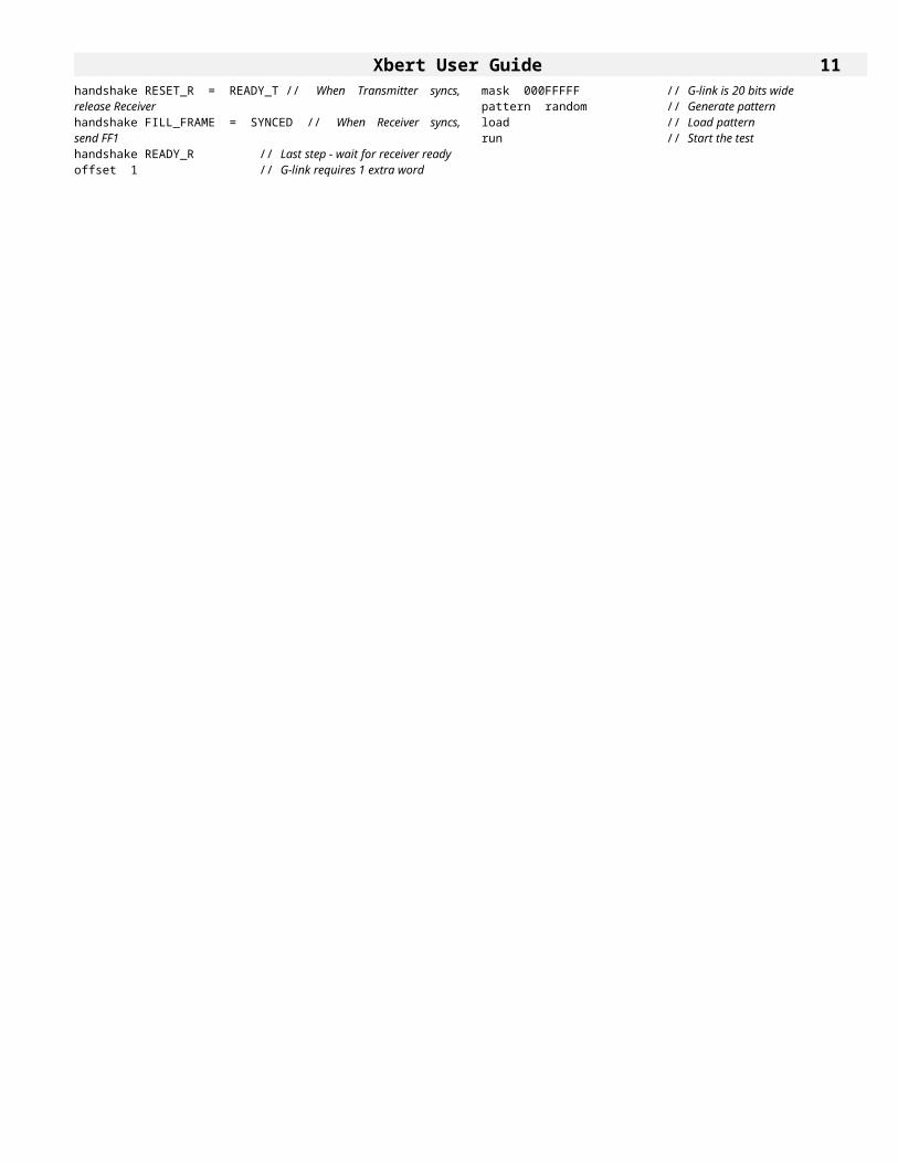
logfile test3.log // Open Log filechip tbert.xcf rbert.xcf pbert.xcf // Load new FPGA filesclock 44 one_edge sync dav_free // Set clock parametersnew_flags // Clear existing definitionsflag C RUN_T // Define RUN flagflag 8 READY_T // Transmitter readyflag 0 RESET_T // Transmitter resetflag 2 DIV1_T // PLL speedflag 3 M20_T // 16/20 bit selectflag 1 FILL_FRAME // Fill frame controlflag 1C RUN_R // Receiver RUNflag 18 READY_R // Receiver readyflag 10 RESET_R // Receiver Resetflag 11 DIV1_R // PLL speedflag 12 M20_R // 16/20 bit selectflag 5 SYNCED // Receiver is synchronizednew_handshake // Define a new handshake sequencehandshake /DIV1_T /DIV1_R M20_T M20_R = // Set operating modes handshake /RESET_R /RESET_T /FILL_FRAME = // Reset deviceshandshake RESET_T = // Release transmitterhandshake RESET_R = READY_T // When Transmitter syncs, release Receiverhandshake FILL_FRAME = SYNCED // When Receiver syncs, send FF1handshake READY_R // Last step - wait for receiver readyoffset 1 // G-link requires 1 extra wordmask 000FFFFF // G-link is 20 bits widepattern random // Generate patternload // Load patternrun // Start the test

Xbert User Guide 10
Notes on Supported Links
ECL 50-Pin ConnectorThe 50-pin connector is intended to be used with adapter cards and very short cables. It has 32 data bits, strobe, and some handshake signals. It also has pins that supply +/- 5 volts. Signal levels are 100K ECL.
Using the loopback test cableOnly use the loopback cable that is supplied with the Xbert. It has been modified so that it doesn’t pass the +/- 5 volt power and so that asserts the READY signal. Other cables will not work properly. If you need to make a loopback cable, simply cut the outer 2 wires on each edge of the cable, and short wires 33 and 34 together.
To run a loopback test, use the LOOPBACK.XBR startup script.
See the HREF="#Interfacing for a complete description of signal names and functions.
Fig 7 ECL 50-pin connector pinoutsTransmitter Receiver
+5V 50 49 +5V +5V 50 49 +5VD31 48 47 D30 D31 48 47 D30D29 46 45 D28 D29 46 45 D28D27 44 43 D26 D27 44 43 D26D25 42 41 D24 D25 42 41 D24D23 40 39 D22 D23 40 39 D22D21 38 37 D20 D21 38 37 D20
GPI3 36 35 GPO3 GPO3 36 35 GPI3GPO0 34 33 READY GPO0 34 33 READYGPI2 32 31 GPO1 GPO2 32 31 GPI1GND 30 29 GND GND 30 29 GNDSTB+ 28 27 STB- STB+ 28 27 STB-GND 26 25 GND GND 26 25 GNDDAV 24 23 GND DAV 24 23 GNDD19 22 21 D18 D19 22 21 D18D17 20 19 D16 D17 20 19 D16D15 18 17 D14 D15 18 17 D14D13 16 15 D12 D13 16 15 D12D11 14 13 D10 D11 14 13 D10
D9 12 11 D8 D9 12 11 D8D7 10 9 D6 D7 10 9 D6D5 8 7 D4 D5 8 7 D4D3 6 5 D2 D3 6 5 D2D1 4 3 D0 D1 4 3 D0
-5V 2 1 -5V -5V 2 1 -5V
Xbert User Guide 11Finisar / G-linkFinisar G-link modules connect directly to the Rbert and Tbert via 60-pin high-density connectors. The G-link uses a single-edged, synchronous, inverted clock.The Rbert clock jumper (Fig 5) should be set to “inverted” and the startup script should set the clock to SYNC, ONE_EDGE, and DAV_FREE.
As shown in Fig 8 the Xbert has access to handshake lines as well as the 16/20-bit word width selection (M20SEL) and one of the PLL clock range signals (DIV1). Fig 10 shows how the handshake signals should be sequenced at startup. Table 1 shows available operating speeds and word widths. Note that the G-link specification says that the maximum word rate in 20-bit mode is 62.5 MHz. This rate can be exceeded if external cooling is used.
Fig 8 Connections from Xbert to Finisar
Data FinisarSTB G-LinkDAV ReceiveRESETDIV1M20SELSTAT0STAT1
Data FinisarSTB G-LinkDAV TransmitRESETFFDIV1M20SELLOCKED
DataTbert STB
DAVGPO0GPO1GPO2GPO3
READY
DataRbert STB
DAVGPO0GPO2GPO3
READYGPI1

Xbert User Guide 12To run a test with the Finisar / G-link module, use the GLINK16.XBR or GLINK20.XBR startup script.
Fig 9 G-Link / Finisar Connector pinouts
Table 1 Finisar/G-link Operating Speeds
Width (M20SEL) DIV1=0 DIV1=116-Bit (0) 42-63.5 16-25 MHz20-Bit (1) 35-62.5 16-21 MHz
ReceiverGnd (D) 31 1 Vcc (D)
DIV1 32 2 DIV0ERR 33 3 Gnd (E)D 1 34 4 D 0D 3 35 5 D 2D 5 36 6 D 4D 7 37 7 D 6
Gnd (E) 38 8 D 8D 10 39 9 D 9D 12 40 10 D 11D 14 41 11 D 13D 16 42 12 D 15D 18 43 13 D 17
Gnd (E) 44 14 Gnd (E)CAV~ 45 15 D 19
LinkRdy~ 46 16 FlagLoopEn 47 17 FF
Active 48 18 DAV~FDis 49 19 Rx_Sig_Det
Gnd (E) 50 20 Strb-Eqen 51 21 Strb+
Opt_Pwr 52 22 SimClk-Sys2 53 23 SimClk+Sys1 54 24 Stat1
FlagSel 55 25 Gnd (E)VEE 56 26 Stat0VEE 57 27 M20Sel
SmRst1~ 58 28 VTTSmRst2~ 59 29 VTT
Gnd (E) 60 30 Gnd (D)
TransmitterGnd (E) 31 1 Gnd (D)
Lock 32 2 VTTM20sel 33 3 VTTVee (E) 34 4 FlagselVee (E) 35 5 Gnd (E)CAV~ 36 6 DAV~Strb+ 37 7 FFStrb- 38 8 EDFlag 39 9 D 0
Gnd (E) 40 10 D 1D 2 41 11 D 3D 4 42 12 D 5D 6 43 13 D 7D 8 44 14 D 9
D 10 45 15 Gnd (E)D 12 46 16 D 11D 14 47 17 D 13D 16 48 18 D 15D 18 49 19 D 17
Gnd (E) 50 20 D 19NC2 51 21 Gnd (E)
Ofc_Stat 52 22 DIV1Reset~ 53 23 Loopen
DIV0 54 24 Opt PwrCS~ 55 25 SYS1
SI 56 26 ReadySO 57 27 NC3
SCLK 58 28 SYS2Gnd (E) 59 29 Vcc (D)Gnd (D) 60 30 NC1

Xbert User Guide 13
SVX GRT Quad G-link receiver (Qbert)
This is a special adapter created to test the G-Link Fiber Receiver Transition Board (GRT). Documentation for the GRT can be found on the HREF="http://www-ese.fnal.gov at:
HREF="http://www-ese.fnal.gov/eseproj/svx/vrb/vrb.htm
Fig 10 G-link Startup Handshake
RESET_T Release Trans.LOCKED Xmit PLL lockedRESET_R Release Receiver
STAT1 PLL Freq. LockFF Send Fill Type 1
STAT0 PLL Phase Lock(RUN) Start Test
Fig 11 GRT Quad G-link Receiver
RESET
GLINK 3
GLINK 2
GLINK 1
GLINK 0SWITCH
DataSTBDAVREADYERROR
DataRbert STB
DAVREADY
GPI1GPO0

Xbert User Guide 14The Qbert uses the standard Rbert hardware with a 4-way switch at the front end. This allows the Qbert to select one of four G-links from the GRT card. The length of the Qbert has been extended to accommodate the GRT power connector and data connector.
To run a test with the Qbert, attach a Finisar transmitter to the Tbert and connect its optical cable to one of the G-Link receivers on the GRT. Execute the QBERT.XBR startup script. Select one of the four G-links using the DEV command and start the test using the RUN command.
Since the GRT doesn’t use the G-link handshake signals, the handshake protocol is “open loop” and must rely on timed steps. The Transmitter’s FF signal should be asserted unconditionally one step after the receiver RESET is released.
Fig 12 GRT J3 Data Connector PinoutPIN A B C D E Link O Link 21 D0 GND rsrv GND D02 D1 D2 rsrv D2 D13 GND D3 rsrv D3 GND4 D5 D4 rsrv D4 D55 D6 GND rsrv GND D66 D7 D8 rsrv D8 D77 GND D9 rsrv D9 GND8 D11 D10 rsrv D10 D119 D12 GND rsrv GND D1210 D13 D14 rsrv D14 D1311 GND D15 rsrv D15 GND12 D16 D16 rsrv D16 D1613 D17 GND rsrv GND D1714 D17 D18 rsrv D18 D1715 GND D18 rsrv D18 GND16 D19 D19 rsrv D19 D1917 CAV* GND rsrv GND CAV*18 DAV* READY* rsrv READY* DAV*19 GND READY* rsrv READY* GND20 STRB GND rsrv GND STRB21 STRB* ERROR rsrv ERROR STRB*22 GND ERROR rsrv ERROR GND
Link 1 Link 323 (GND) GND rsrv GND (GND)24 (GND) (GND) rsrv (GND) (GND)25 GND (GND) rsrv (GND) GND26 CAV* GND rsrv GND CAV*27 DAV* READY* rsrv READY* DAV*28 GND READY* rsrv READY* GND29 STRB GND rsrv GND STRB30 STRB* ERROR rsrv ERROR STRB*31 GND ERROR rsrv ERROR GND32 D0 GND rsrv GND D033 D1 D2 n/c D2 D134 GND D3 n/c D3 GND35 D5 D4 n/c D4 D536 D6 GND (GND) GND D637 D7 D8 (GND) D8 D738 GND D9 (GND) D9 GND39 D11 D10 (GND) D10 D1140 D12 GND (GND) GND D1241 D13 D14 n/c D14 D1342 GND D15 n/c D15 GND43 D16 D16 n/c D16 D1644 D17 GND n/c GND D1745 D17 D18 n/c D18 D1746 GND D18 RESET* D18 GND47 D19 D19 MODID D19 D19

Xbert User Guide 15
Fig 13 GRT J0 Power ConnectorPIN Z A B C D E F1 Gnd +5V +5V +5V +5V +5V Gnd2 Gnd rsrvd rsrvd +5V rsrvd rsrvd Gnd3 Gnd rsrvd rsrvd rsrvd rsrvd rsrvd Gnd4 Gnd Vt User User User User Gnd5 Gnd Vt User User User User Gnd6 Gnd RET_ZT User User User User Gnd7 Gnd AREF_AT User User User User Gnd8 Gnd RET_ZT User User User User Gnd9 Gnd Vz User User User User Gnd10 Gnd Vz User User User User Gnd11 Gnd -5.2V (Vy) User User User User Gnd12 Gnd -5.2V (Vy) User User User User Gnd13 Gnd RET_XY User User User User Gnd14 Gnd AREF_XY User User User User Gnd15 Gnd RET_XY User User User User Gnd16 Gnd -5.2V (Vx) User User User User Gnd17 Gnd -5.2V (Vx) User User User User Gnd18 Gnd rsrvd User User User User Gnd19 Gnd rsrvd User User User User Gnd

Xbert User Guide 16
TTL-Level XbertThe TTL Xbert is almost identical to the ECL version
except that it has TTL-level signals. Connector pinouts are shown in Fig 14 TTL Xbert Transmitter connectors and Fig 17.
Some of the timing relationships of the signals are also different, since TLL is somewhat slower technology. Timing diagrams will be included in the HREF="#Interfacing when they are available.
Fig 14 TTL Xbert Transmitter connectors
Fig 15 Jumper Settings for TTL R-bert ClockThe jumper block allows independent selection of the clock source for the FPGA and input register.The input register can be configured as an edge-triggered register, a latch, or a buffer.
Fig 16 Jumper Settings for TTL T-bert ClockJ3 allows you to select the on board PLL or Crystal as the system clock source.
Note also that the software clock modes allow selection of PLL/XTAL and RISING/FALLING. Selecting XTAL will disable the PLL output. Selecting FALLING will invert the output clock (TCLK) relative to the output register’s clock.
50-Pin connectorD0 1 2 GNDD2 3 4 D1D4 5 6 D3D6 7 8 D5D8 9 10 D7
GND 11 12 D9D10 13 14 D11D12 15 16 D13D14 17 18 D15D16 19 20 D17D18 21 22 GNDD20 23 24 D19D22 25 26 D21D24 27 28 D23D26 29 30 D25
GND 31 32 D27D28 33 34 D29D30 35 36 D31
DAV 37 38 GNDGND 39 40 TCLK+RDY 41 42 GND
CNT1 43 44 CNT2STAT1 45 46 STAT2
GND 47 48 GND+5V 49 50 +5V
60-Pin connectorD0 31 1 GNDD2 32 2 D1D4 33 3 D3D6 34 4 D5
GND 35 5 D7D8 36 6 D9
D10 37 7 D11D12 38 8 GNDD14 39 9 D13D16 40 10 D15D18 41 11 D17
GND 42 12 D19D20 43 13 D21D22 44 14 D23D24 45 15 D25D26 46 16 GNDD28 47 17 D27D30 48 18 D29
DAV 49 19 D31GND 50 20 GND
TCLK+ 51 21 TCLK-GND 52 22 GNDRDY 53 23 CNT0
CNT2 54 24 CNT1GND 55 25 CNT3
STAT0 56 26 STAT1STAT2 57 27 STAT3
GND 58 28 GND+5V 59 29 +5V
nc 60 30 nc
GndReg LE
VccReg ClkFPGA Clk
RCLK-RCLK50
RCLK+
Registered
Latched
Buffer
Input Register Mode
Edge Select
Rising Edge
Falling
Clock Source
J3PLL
XtalClock

Xbert User Guide 17
Fig 17 TTL Xbert reciever connectors
50-Pin connectorD0 1 2 GNDD2 3 4 D1D4 5 6 D3D6 7 8 D5D8 9 10 D7
GND 11 12 D9D10 13 14 D11D12 15 16 D13D14 17 18 D15D16 19 20 D17D18 21 22 GNDD20 23 24 D19D22 25 26 D21D24 27 28 D23D26 29 30 D25
GND 31 32 D27D28 33 34 D29D30 35 36 D31
DAV 37 38 GNDGND 39 40 RCLK50RDY 41 42 GND
STAT1 43 44 STAT2CNT1 45 46 CNT2GND 47 48 GND+5V 49 50 +5V
60-Pin connectorD0 31 1 GNDD2 32 2 D1D4 33 3 D3D6 34 4 D5
GND 35 5 D7D8 36 6 D9
D10 37 7 D11D12 38 8 GNDD14 39 9 D13D16 40 10 D15D18 41 11 D17
GND 42 12 D19D20 43 13 D21D22 44 14 D23D24 45 15 D25D26 46 16 GNDD28 47 17 D27D30 48 18 D29
DAV 49 19 D31GND 50 20 GND
RCLK+ 51 21 RCLK-GND 52 22 GNDRDY 53 23 CNT0
CNT 2 54 24 CNT1GND 55 25 CNT 3
STAT 0 56 26 STAT1STAT 2 57 27 STAT 3
GND 58 28 GND+5V 59 29 +5V
nc 60 30 nc
Note that the pinout of CNT[3:0] and STAT[3:0] shown here is different from earlier documents. This is the correct pinout as of May, 1998

18Interfacing Guide
There are two ways to interface a new link type to the Xbert. HREF="#Daughterboard: If the link can use ECL signal levels and has minimal space and power requirements, then it can be attached as an adapter card to the ECL 50-pin Connector. HREF="#Integrated If it needs TTL level signals or has very tight timing requirements, then a link interface can be integrated with the Xbert circuitry and placed on a custom PC card.
Daughterboard AdapterFig 7 shows the pinouts for the 50-pin ECL connector. All signals are 100K ECL levels. Outputs are terminated with 510 Ohms to VEE. Inputs are terminated with 100 Ohms to -2.5V, except for STB on the Rbert which is a differential signal and is terminated with 100 Ohms across STB+ and STB-.
Transmitter SignalsSTB The strobe is a free-running clock that sets the data
word rate. It is synchronous to DATA and DAV. Fig19 shows the relationship between STB, DATA, and DAV for the Tbert.
DATA The 32 DATA lines are synchronized to the STB via a registered TTL-to-ECL converter. Their timing is such that they should meet a 10ns setup time and 0ns hold time relative to a 16ns STB signal. While a test is starting, the DATA lines contain the contents of pattern word 0 until DAV- is asserted.
DAV- This indicates that data is valid. It is active low. It has the same timing as DATA. This signal remains high until all of the handshake requirements are met and a run signal is sent to the Tbert. When the first valid data word is sent, DAV- drops low and stays low until an error occurs or the test is stopped.
READY This signal is an active-high input. It signals when the test link is synchronized and ready to accept data. If this signal goes low after DAV is low, then the transmitter is stopped and the Data_link_error flag (bit 9) is set in the status register.
GPO[3:0]These are general-purpose software-controlled outputs. They are controlled using the handshake
commands. GPO2 is not available on the 50-pin connector.
GPI[3:0] These are general-purpose input flags. They can be used by the handshake commands. GPI0 and GPI1 are not available on the 50-pin connector.
+5V,-5V These are power supply pins. A daughterboard should not draw more than 4 amps from them. They should not be used with a cable.
Receiver SignalsSTB Timing requirements for the STB, DAV, and DATA
signals are shown in Fig 18. Also see the discussion on HREF="#Clocking_Schemes below.
DATA 32 data inputs. Since these are terminated to -2.5V, any unused inputs should be left floating. Use the HREF="#C_Mask command to mask off unused inputs.
DAV- This active-low signal can be used to qualify the STB signal. It also has an internal latch that allows it to be used as a start-of-test signal (see HREF="#Clocking_Schemes).
READY This signals when the test link is synchronized and ready to accept data. If this signal goes low after the test has started, then the receiver is stopped, the current data word and pattern address are latched, and the Data_link_error flag (bit 25) is set in the status register.
GPO[3:0]General-purpose outputs. GPO1 is not available on the 50-pin connector.
GPI[3:0] general-purpose inputs. GPI0 and GPI2 are not available on the 50-pin connector.
Fig 18 Receiver clock timing
Fig 19 Transmitter Timing
XCLKSTB
DATA
0.4ns1.4ns
4.0ns2.0ns
5nsRCLK
STBDAV-
Dual Edged
RCLKSTB
DAV-
Single Edged
8ns3ns
STB
DAV-
RCLK
DATA
XCLK
DATADAV-
PatternRAM
STB+STB-
50-PinConnectorTTL
toECLREG
.
15ns5ns
STB
DAV-
RCLK
DATA

19Clocking SchemesThe Rbert can handle several variations on the clock/data relationship. These variations are controlled by three flags (See the HREF="#C_Clock command) and the Clock Inversion Jumper (Fig 5). Variations include:
Single Edged:
Data is sampled near the falling edge of the STB. This is typically used for links that re-synchronize data at the receiver. Data can change on the rising STB and has at least ½ clock cycle to settle.
Dual Edged:Data is sampled 5-10ns after either clock edge. This can be used with parallel links that don’t re-synchronize data. The clock is embedded in the pattern and so has the same bandwidth as the data bits and very little skew relative to the data bits. The HREF="#C_Clkbitcommand will set a selected pattern bit to be a dual-edged clock.
Synchronous:The clock is a constant frequency and does not stop. Valid data is indicated by a low on DAV-. This is typical of serial links.
Asynchronous:The clock transitions only when valid data is sent or when the link is active. DAV- is not necessary, but it may be used to qualify data.
DAV Hold:Some links may not have a DAV signal. In this case, a signal is needed to indicate the start of a test. A selected data bit can be used for this purpose by tying it to the DAV- pin. The first transition on the data bit will be latched and used to gate the clock.Use the HREF="#C_Davbit command to embed a DAV signal into a pattern. Note that since the first transition occurs on word 1, the HREF="#C_Offsetcommand should be used to make sure the receive pattern is aligned correctly with the received data.
DAV Free:The DAV- signal is not latched internally and is used to qualify every clock.
MechanicalTo fit in the standard Xbert box, an adapter card should have the dimensions shown in Fig 20.
The connector should be a standard 50-pin .1” female header. (3M part #?????? Fermilab stock #??????)
Fig 21 DAV-HOLD timing
Fig 20 Adpater card dimensions
STBDATA
(internal DAV-)RCLK
Word 1Word 0
0“
Top ViewMechanical Drawing to be
added later 0“
Side view 0“
0“

20Integrated AdapterAll of the signals described in the HREF="#Daughterboard section are available for use by an integrated adapter. The signals can be TTL or ECL levels. The TTL-level data lines from the Tbert come directly from the pattern RAM chip and have an 8ns clock to output delay.The TTL circuits of the Tbert and Rbert require +5V. An on board 3.3V converter is used for the memory chip and could supply an extra 500ma of 3.3V to other devices. The -5V supply is not necessary if no ECL circuits are used.
The total size of an integrated adapter should be 3.9 x 9.9 inches in order to fit in the standard Xbert box.
Fig 22 TTL Tbert timing
XCLKDATA
8.0ns2.0ns
XCLK
DATA
DAV-
PatternRAM

21Debugging Guide
This section contains a map of the hardware and software modules with a brief description of each. Schematics are all in PDF format.
Common Elements
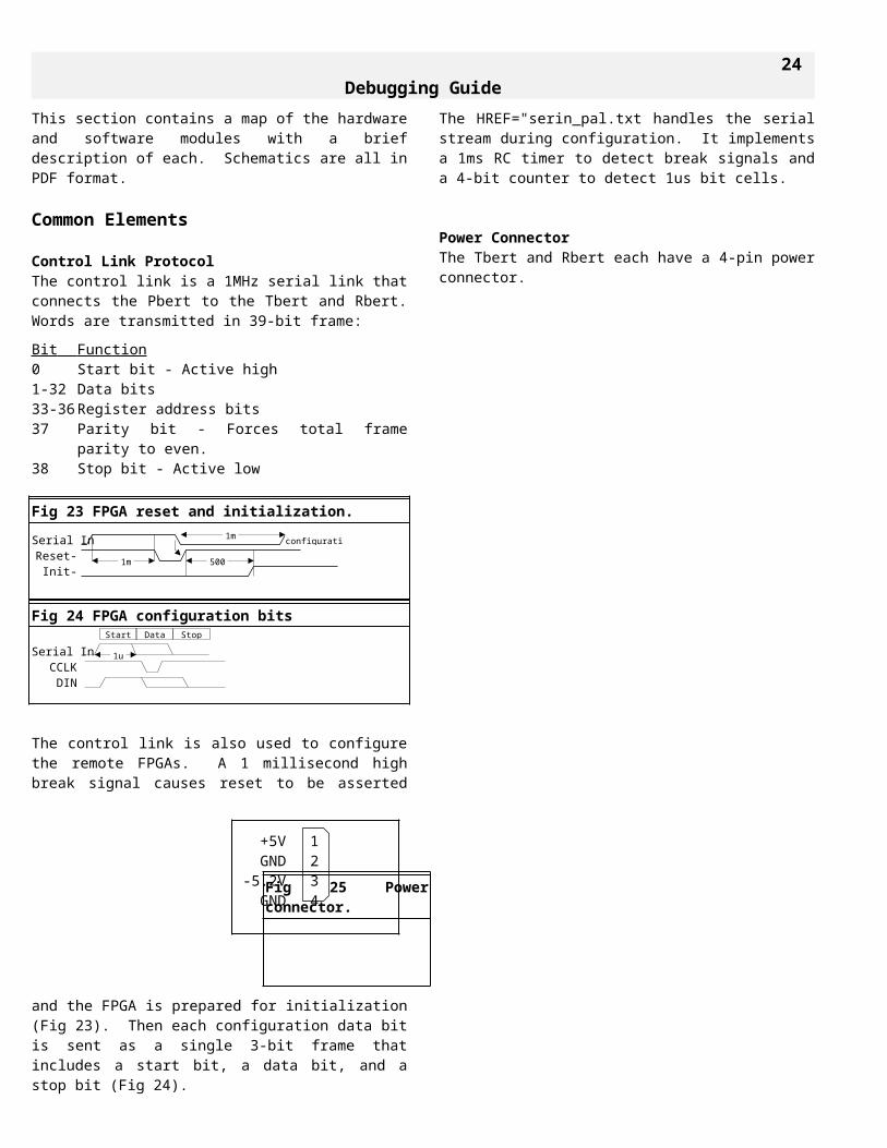
Control Link ProtocolThe control link is a 1MHz serial link that connects the Pbert to the Tbert and Rbert. Words are transmitted in 39-bit frame:
Bit Function 0 Start bit - Active high1-32 Data bits33-36 Register address bits37 Parity bit - Forces total frame parity to even.38 Stop bit - Active low
The control link is also used to configure the remote FPGAs. A 1 millisecond high break signal causes reset to be asserted and the FPGA is prepared for initialization (Fig 23). Then each configuration data bit is sent as a single 3-bit frame that includes a start bit, a data bit, and a stop bit (Fig 24).
The HREF="serin_pal.txt handles the serial stream during configuration. It implements a 1ms RC timer to detect break signals and a 4-bit counter to detect 1us bit cells.
Power ConnectorThe Tbert and Rbert each have a 4-pin power connector.
FPGA filesFpga files are developed using Workview/Office and Orca Foundry 7.1. Source files are in the Xbert/fpga directory. Routed FPGA files are in the Xbert/fpga/routed directory. Do
not make any changes in the routed directory unless you are sure you know what you are doing.
Reading the FPGA schematicsThe schematics contain a large number of function generator symbols. A function generator is a single output pin associated with a logic equation. They come it two varieties: combinatorial (UFUNC) and registered (QFUNC). The QFUNC can take attributes to specify register control signals.
Compiling FPGA schematicsIf you need to make minor changes to the FPGAs, you can edit and re-compile the FPGA schematics. Editing schematics requires the Workview/Office software to be installed. Compiling schematics requires the ORCA Foundry software to be installed. Each FPGA file has an associated .bat file for compiling, place, and route. The .bat files should be run in a DOS window.
To compile a schematic to an un-routed .ncd file, use the .bat file with the CHECK option. This creates a mapping log file (.mog) which should be checked for error messages and resource usage. Resource usage should be close to that in Table 2. If it’s much less, then check the .mrp file for reports of removed logic.
To place and route, use the PAR or PARG option. The PARG option uses the existing part as a guide and works best if minor changes were made to the schematics. If major changes are made, then the PAR option should be used. The router makes several attempts and saves them in a separate folder (T1.dir, R1.dir, or P1.dir). A summary file (*.par) lists the results. The
Table 2 FPGA resource usage
PFUs TBUFs External PICsTBERT 79 107 68RBERTPBERT 84 64 49
Fig 24 FPGA configuration bits
Serial InCCLK
DIN
Fig 26 Function generator symbols
UFUNC: U=<equation> Output
QFUNC: Q=<equation> Registered_Output
Qfunc Attributes:K=<clock_signal> Default clock name is “CLK”CE=<clock_enable>RD=<reset_direct> Asynchronous resetSD=<reset_direct> Asynchronous setRS=<reset_direct> Synchronous resetSS=<reset_direct> Synchronous set
Fig 23 FPGA reset and initialization.
Serial InReset-
Init-
+5V 1GND 2-5.2V 3GND 4Fig 25 Power connector.
configuration bits
1ms
500us
1ms
StopDataStart
1us

22best result should be tested before moving it to the routed folder.
To create a bit file, use the BIT option.
PBERTHREF="unavailable.HTMThe Pbert consists of an ISA connector, an ISA address decode PAL, an FPGA, and several RS-485 drivers for the control link.
HREF="isapal.txt (Current Checksum = 73AE)
FPGA Schematics:HREF="pbert_fpga.pdf Top level schematic.HREF="serinh.pdf Serial input port (Control Link).HREF="serofif.pdf Serial output port with FIFO.
TBERTHREF="unavailable.htm
FPGA Schematics:HREF="tbert_fpga.pdf Top level schematicHREF="clkspeed.pdf Clock speed control circuitHREF="serin.pdf Serial input port (Control Link).HREF="serout.pdf Serial output port.
RBERTHREF="unavailable.htm
HREF="clock_pal.txt
FPGA Schematics:HREF="rbert_fpga.pdf Top level schematicHREF="rcmp.pdf Comparator Pipeline.HREF="cmp_reg.pdf Comparator register primitive.HREF="serin.pdf Serial input port (Control Link).HREF="serout.pdf Serial output port.
Fig 28 RBERT block diagram
Fig 27 TBERT block diagram
32Synchronous
SRAM
ReadyStatusControl
Link Circuitry
Data
ClockDav-
32
FPGA
AddressSequencer
ControlLink
Compare
FLAGS4
4
15
TRANSLATORS
32
ReadyStatusControlDav-
Link Circuitry
Clock
Data32
ClockPAL
SynchronousSRAM
ClockGenerator
4TRANSLATORS15
4
FPGA

Debugging Guide 23SoftwareThe software was developed using Borland C 5.0. To build a new version, use the makefile, Xbert.mak, or the ide file Xbert.ide. The following source files are needed:
HREF="xbert_c.txt Main source code.HREF="box_c.txt Routines for drawing boxes and menus.HREF="xbert_h.txt Include file for register definitions.HREF="box_h.txt Box include file.HREF="bit2brt_c.txtSource code for fpga bit-file converter
Hardware Register Formats
Pbert registersThe Pbert is essentially a dual serial link controller. Its registers are used to send and receive 36-bit words from the Tbert and Rbert. Each word consists of 32 data bits and 4 address bits which specify the remote Tbert or Rbert register.
The Pbert has eight 16-bit registers starting at the location set by the base address dipswitch.
Writeable Pbert registersTo send a data word requires three writes: two 16-bit halves of the data word and one 4-bit write to set the remote register address and send it out the serial link.Offset Name Function
0 Lconfig Local configuration (reset, parity enable, etc.)2 SendX Set 4-bit register address and send current data to Tbert.4 SendR Send Rbert6 SendXR Send to botha DataX Set transmitter data for Tbert 16 bits at a time.c DataR Set transmitter data for Rbert 16 bits at a time.e DataXR Set transmitter data for Both 16 bits at a time.
Readable Pbert registers A remote module sends the contents of one of its registers when it receives a read request (remote registers 8-f). That data is saved in the 32-bit Xdata or Rdata register. When there is no request, the remote modules send status and cycle count. These are saved in the Xcycle, Rcycle, Xstatus, and Rstatus registers:Offset Name Function
0 Xcycle Tbert cycle count2 Xstat Tbert Status
4,6 Xdata 32-bit Tbert Data8 Rcycle Rbert cycle counta Rstat Rbert Status
c,e Rdata 32-bit Rbert data
Lconfig register bit definitionsMask Name Function 001 Break Send break signal (Reset remote modules - clear FPGA)002 Parity Disable parity - (used to download FPGA)004 ErClr Clear Pbert Errors (overrun / parity errors)008 Reset Clear Pbert FPGA and prepare to reload0e0 ChSel Channel select - Select channels 0-3 or use 4 for loopback.100 SetCh Set Channel - must be 1 to change the ChSel field.
Status register bit definitions (Xstat, Rstat)Bits 3:0 are local to the Pbert interface:0001 Sempty No Status received since last read.0002 Rempty No data received since last read.0004 Full Control link output FIFO is full.0008 C_err Control link got an error.Bits 15:4 come from the remote module00f0 Gpi[3:0] State of Gpi inputs0100 Ready Link ready0200 Lnk_Err Link Error0400 Si_Err Control Link Error at remote end.0800 Cmp_Err Compare Error1000 Run Run/Idle state2000 Dav Data available is asserted8000 Error One of the Error bits is on.
Remote writeable registers1 State Set operating state (Run, Stop, Flags)2 Config Set clock configuration4 Wram Write 32 bits to RAM using internal Addr pointer5 Cram Compare 32 bits to RAM. Set Cmp_Err if different.6 Wram+ Write to RAM and increment Addr7 Cram+ Compare to RAM and increment Addr
Remote readable registers9 Eword Send tha data word that caused a compare error (RBERT only)A Addr Send contents of Addr in bits 14:0C Rram Read from RAM and send 32-bit dataE Rram+ Read from RAM and increment Addr
Remote register #1: State register bits0001 Idle Set device to Idle0002 Run Start test0010 ErClr Clear Errors0020 AdClr Clear Addr register to 00040 CyClr Clear Cycle counter to 00080 GpoSet Set Gpo outputs0f00 Gpo[3:0] State of Gpo outputs1000 SoHold Hold Serial link
Remote register #2: Clock configuration register7f0000 Clock speed from 16.0 to 63.5mhz in .5mhz steps.000030 Receiver device select - Select one of 4 devices.000004 ASYNC000002 DAV_HOLD000001 TWO_EDGE
Program FlowThe main program loop does three things:Check for fatal: if some routine has detected a fatal error, it
sets the global Fatal flag. Try to re-initialize all of the hardware.
Decode status: update status and statistics display. Log errors.Accept command: Characters are accepted from the keyboard
one at a time without interrupting the main loop. The command is processed when enter is pressed.
Debugging Guide 24Subroutine Descriptions
Hardware access macros:Xcycle Return current hardware cycle countRcycleXstat Return Current hardware statusRstatXdata Return Current DataRdataLconfig(Dat) Set local configurationSendX(Reg,Dat) Send Data to remote registerSendR(Reg,Dat)SendXR(Reg,Dat)WaitX Wait for serial link FIFO to be un-fullWaitRWaitXR
Subroutines:void Plog(char *S) Print to logPlog1(T,V) Formatted Plog with 1 variablePlog2(T,V1,V2) Formatted with two variables
void ABox(int X1, int Y1, int X2, int Y2, int Type)Draw an ASCII box (Type= single or double)
void More(char *File)Display a file
void Set_port(int N)Set serial port to 0-3 or local (4)
void NameFlag(int F, char *N) Attach a user-supplied name to a flag
void Set_ext(char *Name, char *Ext, int Flag)Set or force file extension
void Pattern(char *Type) Make a pattern
int Parse(char *S)Split line into words
void Clink_msg(char *T, char M, int S )Decode control link errors
long Valid_Status(char *Txt)Fetch a valid status from the remotes
int ReadReg(int Reg, int Rx)Read a remote register and place in DataX or DataR global
int Sanity_check(int Level) Level 0: All 1: Local only
void ComFile(char *F)Open command file
FILE * OpenFile(char *Name)Open bit file
int Load_bit(void)Reset and load ORCA chips, Do a sanity check. Return 0 if successful. Update Loaded global.
int Load_pat(int Check)Load or check pattern into remote modules(Check=1) => Check only(Check=2) => Load then check(Check=3) => Check then load if necc.
void Draw_screen( int Level )Draw boxes and fill in configuration data
int Decode_Status(char *Txt)Detect and log errors and bursts. Do handshake steps. Update flags and statistics on screen
int Make_Idle(void)Make remotes idle. Return 0 if success
void Run(void)void Stop(void)void Clear(void)
Error Messages%s <RT>bert Control link error.
When trying to access a remote module, there was a data-overrun or parity error. This is probably due to a program error, but could be caused by faulty connections.
%s Not Receiving status from <RT>bert.The remote modules should report their status every 80 microseconds. This error indicates that the remote module has probably failed.
%s <RT>bert Control link error at remote end.The remote module received a parity error or overrun error. This is probably due to noise, but could be a program error.
There is a fatal control link error.A permanent control-link problem makes it impossible to communicate with the remote modules. The software will attempt to re-initialize the system.
Invalid register (%d) in ReadRegParameter error in ReadReg (Rx=%d)
These two messages indicate a software error. You should find the programmer and smack him in the head.
ReadReg failedThe software issued a read request but never got a response. This indicates a hardware problem.
Couldn't set <TR>bert to idle.Wrote to the Idle bit, but the status won’t change.
Sanity Check Data Error: %s: expect %lx, got %lxThe sanity check first checks that it can send data in local loopback mode, and then tries to write and read the remote memory. If these fail, it indicates a hardware problem.
Local sanity check failed with error status %xThis indicates a problem either the control-link hardware. Since this is mostly in the FPGA, the system should be re-initialized.
Remote Sanity check failedSanity check of remote modules failed.

Debugging Guide 25Timeout while loading PBERT bit file. Check Hardware
The very first step of initializing the Pbert has failed. This indicates the Pbert is missing or has the wrong base address.
Pattern file is wrong sizeA pattern file must be exactly 128Kbytes.
Unrecognized pattern type [name]The = character is used to indicate standard pattern types, however the name is not recognized. If you want to load a pattern file, don't include the =.
Load_pat: No pattern has been specifiedLoad has been requested before a pattern has been set.
Check <TR>bert: Adr=%4.4x Got %8.8lx Expect 8.8lxThe pattern at the remote node got corrupted.
data tsync rsync Adr=#### Got=######## Expect=######## Link error. This was caused by the link being tested.
Burst error....Several link errors in a row. The software will check the pattern in case this was caused by a corrupted pattern.
Fatal burst error....Several more link errors. The software will reset and reload the FPGA files.
Attempting to re-initializeIf a fatal error occurs, then the system is reset and re-initialized.
Program Halt. Press ENTER to continueIf too many fatal errors, then stop and wait for user intervention.
Invalid clock speed [%s]The clock speed must be 16.0 to 63.5 MHz.
Unknown clock configuration [%s]One of the clock configuration words is mis-spelled.
Handshake: Flag <xxx> not foundA Flag name was mis-spelled or never named.
Unrecognized command [%s]A command was misspelled