x-ray magnetic circular dichroism study of oxide-based...
TRANSCRIPT

X-ray magnetic circular
dichroism study of oxide-based
magnetic materials and
half-metallic alloys
Doctor Thesis
Vijay Raj Singh
Department of Physics, University of Tokyo
July, 2011


Abstract
The study of spintronics materials such as diluted magnetic semiconduc-
tor (DMSs), multiferroic and half-metallic alloys is one of the most attractive
fields in science from the viewpoints of both academic research and applica-
tions. In order to clarify the origin of ferromagnetism of these spintronics, it is
necessary to investigate the electronic structure. In this thesis, we have inves-
tigated the electronic structure of spintronics materials using x-ray absorption
spectroscopy (XAS) and x-ray magnetic circular dichroism (XMCD).
The first discovery of room-temperature ferromagnetism in Co-doped
TiO2 by Matsumoto et al. [1] has arisen great interest in the search for such
materials and a number of studies have been carried-out to investigate whether
the ferromagnetism is carrier-mediated or not [2-3], but the issue still remains
controversial. XMCD at the Co 2𝑝 → 3𝑑 absorption (Co 𝐿2,3) edge is an ideal
technique to clarify this issue because it is an element-specific magnetic probe.
Our previous XMCD study has revealed that the ferromagnetism is not due
to segregated Co metal clusters but is due to Co2+ ions in the TiO2 matrix
[4]. However, the XMCD signal intensities were an order of magnitude lower
than that expected from the bulk magnetization [4]. We performed XAS and
XMCD studies on rutile Co-doped TiO2 by the surface-sensitive total electron
yield (TEY) mode and the bulk-sensitive total fluorescence yield (TFY) mode
and found that Co ions in the bulk indeed have a large moment of 0.8-2.2 𝜇𝐵
/Co [5]. Then we extended the same approach to anatase Co-doped TiO2 and
studied the correlation between magnetism and transport properties.
Further we performed the XAS and the XMCD studies of (1-𝑥) BiFeO3-
𝑥BiCoO3 (BFCO) thin films (where 𝑥 = 0 to 0.30) grown on LaAlO3(001)
substrates using a chemical solution deposition technique. The XAS results
indicated that the Fe ions were in the Fe3+ state and that the Co ions were in
the Co3+ state. XMCD results showed that the Fe ions were in ferromagnetic
state and the Co ions were in the paramagnetic state at room-temperature.
The XMCD measurements also revealed that antiferromagnetically coupled
Fe3+ ions were at the 𝑂ℎ and 𝑇𝑑 sites. The magnetic moment of the Fe ions
increased up to 20% Co content and after that it decreased. However, the Co
magnetic moment was nearly independent of Co content unlike Fe, and the
peak at 20% Co showed only a minor influence. The magnetization deduced
from XMCD is larger than that obtained by SQUID measurements, indicates

the enhancement of ferromagnetism within ∼ 5 nm from the surface, probed
by the total electron yield (TEY) method.
Finally we studied the magnetic and electronic states of Co2Mn𝛽Si0.88(CMS)/MgO and Co2Mn𝛽Ge0.38(CMG)/MgO magnetic tunnel junctions by
means of XMCD measurements. In particular, the Mn composition (𝛽) depen-
dences of the Mn and Co magnetic moments were investigated. As 𝛽 increases
in the CMG films, the spin magnetic moment of Mn decreases, consistent with
Picozzi et al.’s calculations [6] which predicts that the Mn magnetic moment
couples antiferromagnetically at MnCo site, leading to a reduction of saturation
magnetization. The Mn 𝐿2,3-edge XAS showed for higher 𝛽 values a Mn2+-
like multiplet structure in MnO, however, for lower values of 𝛽 we did not
obtain Mn2+-like multiplet structure. The Co spin magnetic moment for all
the samples was obviously larger and/or equal to theoretical value of 1.06 𝜇𝐵
[7]. For the Co-rich region, there is the possibility of the existence of CoMn
antisite because experimental value 𝑚spin(Co)=1.3 𝜇𝐵 is larger than that the
calculated value of the bulk, which is 1.06 𝜇𝐵 for Co at the regular Co site,
CoCo, consistent with Picozzi et al. [6]. These Co-rich films composition im-
ply the presence of Co antisites that would lower the spin polarization at the
Fermi level. For the Mn-rich region, 𝑚spin(Co) slightly decreases which is also
consistent with theoretically predicted value. A Co2+-like multiplet structure
in CoO was not observed in any films, indicating that the Co atoms were not
oxidized. For CMS, the 𝑚spin(Mn) behavior was similar to CMG and in this
case we did not observe oxidation of Mn. However, 𝑚spin(Co) was almost in-
dependent of 𝛽. Because the amount of CoMn in Co-rich CMS may be more
or less than that obtained in Co-rich CMG [8].
References
[1] Y. Matsumoto, M. Murakami, T. Shono, T. Hasegawa, T. Fukumura,
M. Kawasaki, P. Ahmet, T. Chikyow, S.-Y. Koshihara and H. Koinuma, Sci-
ence 291, 854 (2001).
[2] H. Toyosaki, T. Fukumura, Y. Yamada, K. Nakajima, T. Chikyow, T.
Hasegawa, H. Koinuma and M. Kawasaki, Nat. Mat. 3, 221 (2004).
[3] S. R. Shinde1, S. B. Ogale, J. S. Higgins, H. Zheng, A. J. Millis, V.N.
Kulkarni, R. Ramesh, R. L. Greene, and T. Venkatesan, Phys. Rev. Lett. 92,
66601 (2004).
[4] K. Mamiya, T. Koide, A. Fujimori, H. Tokano, H. Manaka, A. Tanaka,
H. Toyosaki, T. Fukumura, and M. Kawasaki, Appl. Phys. Lett. 89, 062506
(2006).
[5] V. R. Singh, Y. Sakamoto, T. Kataoka, M. Kobayashi, Y. Yamazaki,
A. Fujimori, F.-H. Chang, D.-J. Huang, H.-J. Lin, C. T. Chen, H. Toyosaki,

T. Fukumura and M. Kawasaki, J. of Phys.: Conds. Matt. 23, 176001 (2011).
[6] S. Picozzi, A. Continenza and A. J. Freeman, Phys. Rev. B 69, 094423,
(2004).
[7] S. Picozzi, A. Continenza and A. J. Freeman, Phys. Rev. B 66, 094421
(2002).
[8] D. Asakura, T. Koide, S. Yamamoto, K. Tsuchiya, T. Shioya, K.
Amemiya, V. R. Singh, T. Kataoka, Y. Yamazaki, Y. Sakamoto, A. Fujimori,
T. Taira and M. Yamamoto, Phys. Rev. B 82, 184419 (2010).
5

Contents
1 Introduction 1
1.1 Spintronics . . . . . . . . . . . . . . . . . . . . . . . . . . . . . . 1
1.2 Diluted magnetic semiconductors . . . . . . . . . . . . . . . . . 1
1.2.1 Theoretical models for carrier-mediated ferromagnetism . 3
1.2.2 Possibility of ferromagnetism in Co-doped TiO2 dilute
magnetic oxide . . . . . . . . . . . . . . . . . . . . . . . 8
1.3 Multiferroics . . . . . . . . . . . . . . . . . . . . . . . . . . . . . 14
1.3.1 Multiferroic materials and magnetoelectric effect . . . . . 14
1.3.2 Single phase multiferroic materials: a brief history [59] . 14
1.3.3 Multiferroic composites . . . . . . . . . . . . . . . . . . . 14
1.3.4 Magnetoelectric effects . . . . . . . . . . . . . . . . . . . 15
1.3.5 Physical properties of BiFeO3 . . . . . . . . . . . . . . . 16
1.3.6 Substitution studies of transition-metal ions in BiFeO3 . 19
1.4 Heusler Alloys . . . . . . . . . . . . . . . . . . . . . . . . . . . . 21
1.4.1 Physical properties of Heusler alloys . . . . . . . . . . . . 21
1.4.2 Heusler half-metals in devices . . . . . . . . . . . . . . . 27
1.4.3 Heusler alloys: disorder and interfaces . . . . . . . . . . 29
2 Experimental Methods and Principles 31
2.1 Principles of x-ray magnetic circular dichroism and sum rules . . 31
2.1.1 X-ray absorption spectroscopy and x-ray magnetic cir-
cular dichroism . . . . . . . . . . . . . . . . . . . . . . . 31
2.1.2 XMCD sum rules . . . . . . . . . . . . . . . . . . . . . . 33
2.1.3 Analysis of x-ray magnetic circular dichroism spectra . . 34
2.2 Experimental setup . . . . . . . . . . . . . . . . . . . . . . . . . 34
2.2.1 NSRRC BL-11A . . . . . . . . . . . . . . . . . . . . . . 34
2.2.2 KEK-PF BL-16A . . . . . . . . . . . . . . . . . . . . . . 36
2.2.3 SPring-8 BL23SU . . . . . . . . . . . . . . . . . . . . . . 36
i
3 X-ray magnetic circular dichroism study of ferromagnetic Ti1−𝑥Co𝑥O2−𝛿
thin films 40
3.1 Introduction . . . . . . . . . . . . . . . . . . . . . . . . . . . . . 40
3.2 Experimental . . . . . . . . . . . . . . . . . . . . . . . . . . . . 41
3.3 Results and Discussion . . . . . . . . . . . . . . . . . . . . . . . 42
3.3.1 Results on rutile Co-doped TiO2 . . . . . . . . . . . . . 42
3.3.2 Results on anatase Co-doped TiO2 . . . . . . . . . . . . 49
3.4 Conclusion . . . . . . . . . . . . . . . . . . . . . . . . . . . . . . 55
4 X-ray magnetic circular dichroism study of ferromagnetic BiFe1−𝑥Co𝑥O3
thin films 56
4.1 Introduction . . . . . . . . . . . . . . . . . . . . . . . . . . . . . 56
4.2 Experimental . . . . . . . . . . . . . . . . . . . . . . . . . . . . 58
4.3 Results and Discussion . . . . . . . . . . . . . . . . . . . . . . . 58
4.4 Conclusion . . . . . . . . . . . . . . . . . . . . . . . . . . . . . . 67
5 Effect of off-stoichiometry in Heusler alloy thin films on spin-
dependent tunneling characteristics of Co2Mn𝛽𝑍/MgO (𝑍=
Ge, Si) magnetic tunnel junction studied by x-ray magnetic
circular dichroism 68
5.1 Introduction . . . . . . . . . . . . . . . . . . . . . . . . . . . . . 68
5.2 Experimental . . . . . . . . . . . . . . . . . . . . . . . . . . . . 70
5.3 Results and discussion . . . . . . . . . . . . . . . . . . . . . . . 71
5.3.1 Magnetic properties of Co2Mn𝛽Si0.88/MgO MTJs as a
function of Mn composition 𝛽 . . . . . . . . . . . . . . . 71
5.3.2 Magnetic properties of Co2Mn𝛽Ge0.38 MTJs as a func-
tion of Mn composition 𝛽 . . . . . . . . . . . . . . . . . 77
5.3.3 Mn and Co antisite defects in Co2MnSi and Co2MnGe . 83
5.3.4 Atom exchange in Co2MnSi and Co2MnGe . . . . . . . . 84
5.3.5 Comparison between Co2MnSi and Co2MnGe . . . . . . 86
5.3.6 Formula unit composition model for nonstoichiometric,
Ge-deficient Co2Mn𝛽Ge0.38 films . . . . . . . . . . . . . . 87
5.4 Conclusion . . . . . . . . . . . . . . . . . . . . . . . . . . . . . . 89
6 Summary and Outlook 91
ii


Chapter 1
Introduction
1.1 Spintronics
Spintronics (a neologism meaning “spin transport electronics”), also known
as magnetoelectronics, is an emerging technology that exploits both the intrin-
sic spin of the electron and its associated magnetic moment, in addition to its
fundamental electronic charge, in solid-state devices [1, 2]. Spintronics is ex-
pected to improve upon traditional electronics and photonics devices, allowing
for enhancement in the form of reduced power consumption, faster device op-
eration, and new form of information computation. Thus new multifunctional
devices including spin valves, quantum bits for quantum computing, spin po-
larized light-emitting diodes and spin polarized field-effect transistors can be
and partially have already been realized [3]. Increased functionalities are also
expected, such as integrated magnetic and electronics operations on the same
chip.
1.2 Diluted magnetic semiconductors
Dilute magnetic semiconductors (DMS) are semiconductors doped with a
small amount of transition metal ions that introduce local magnetic moments.
The coupling between the localized moments and delocalized band-electrons
renders unique properties of DMS, such as a giant spin-splitting of electronic
states and indirect ferromagnetic exchange interactions between magnetic mo-
ments [1]. The latter is controlled by the manipulation of carriers by means
of, e.g., doping, electric fields, optical excitation, and quantum structures,
which are all key technologies within the well-established field of conventional,
charge-based electronics. Therefore, the tunable ferromagnetism attainable in
DMS is one of the leading areas of semiconductor spintronics.
1

The reported DMS materials are summarized in Table 1.1. Most of the
early dilute magnetic semiconductors such as tellurides, selenides and sulfides
were based on Mn-doped II-VI semiconductors. The valence match (i.e. iden-
tical charge state) of the cation of the II-VI host semiconductors to the dopant
(Mn), if they can be doped with charge carriers, makes it easy to prepare
samples with a large amount of Mn [2, 3]. The model materials (i.e. II-VI
materials) in which localized spins and delocalized holes can be introduced
and controlled independently, while dimensional effects can be tested by using
quantum heterostructures [4]. The previous studies showed that the dominant
magnetic interaction between Mn spins is antiferromagnetic in the II-VI type
DMS. It has also been proven difficult to create 𝑝- or 𝑛-type carriers to me-
diate ferromagnetic interactions, resulting in paramagnetic, antiferromagnetic
or spin glass behavior [2, 3]. Irrespective of their effects on fueling magnetism
research, II-VI DMS already found their applications in flat panel displays,
since efficient electroluminescence can be obtained by doping Mn and optical
isolators which allow the transmission of light in only one direction. Ferro-
magnetism was observed at temperatures below 2 K in Mn-based zinc-blende
III-V compounds such as CdMnTe after the result of carrier induced ferro-
magnetism in Mn-based zinc-blende III-V compounds [5]. Recently, Kuroda
et al. [6,7] suggested that Cr rich phases of ZnCrTe showed room temperature
ferromagnetism, causing a stimulation of II-VI DMS. However, its origin at
room-temperature is controversial so far.
In III-V DMS, divalent transition metal ions (Mn) substitute for trivalent
cations, thus generating holes whereas in II-VI DMS, additional doping of 𝑝-
type or 𝑛-type elements is required. The holes introduced by the magnetic ions
mediate ferromagnetic interaction between the magnetic ions in III-V DMS.
The reported Curie temperatures of III-V DMS are generally higher than II-
VI DMS but are still too low below room-temperature and thus for industrial
applications. For (GaMn)As, the highest record Curie temperature in III-V
DMS is 173 K [8]. Recently, room-temperature ferromagnetism have been
reported by several oxides and nitrides. As a matter of fact, the studies by
mean-field Zener model based on RKKY exchange interaction developed by
Dietl et al. [9] aimed at searching robust room-temperature DMS were trig-
gered, which predicts 𝑝-type GaN and 𝑝-type ZnO as promising candidates for
room-temperature DMS. Also because oxides and nitrides were already com-
mon materials for light-emitting devices in industry, this prediction triggering
tremendous works to dope transition metal ions into oxides and nitrides. How-
ever, oxides are naturally 𝑛-type because of oxygen vacancies formed during
the growth, while the mean field Zener model concerns 𝑝-type wide band gap
materials. As an alternative theoretical model, Coey et al. [10] suggested that
2

oxygen vacancies forming a spin-split impurity band may play a vital role in
forming carrier-induced ferromagnetism. It is also reported, however, that
oxygen vacancies act as active sites for forming clusters [11]. In fact, there are
comparable amounts of reports that indicate that the magnetism originates
from segregated clusters magnetic materials in oxides against and reports that
claim intrinsic magnetism. It should be noted that in the latter case a careful
study of the structural properties of the materials is often lacking [12,13].
Table 1.1: Representative dilute magnetic semiconductors.Material Class Material References
II-VI 𝑝-Cd1−𝑥Mn𝑥Te:N [5]
II-VI 𝑝-Zn1−𝑥Mn𝑥Te:N [4]
II-VI Zn1−𝑥Cr𝑥Se [14]
II-VI Zn1−𝑥Cr𝑥Te [15]
IV-VI Pb1−𝑥−𝑦Sn𝑦Mn𝑥Te [16]
III-V In1−𝑥Mn𝑥As [17]
III-V Ga1−𝑥Mn𝑥As [18]
III-V GaMnN [19]
III-V GaCrN [20]
III-V GaMnP:C [21]
III-V GaMnSb [22]
IV Ge1−𝑥Mn𝑥 [23]
Oxide Co-TiO2 [24]
Oxide Mn-ZnO [25]
Oxide Co-SnO2 [26]
Oxide Fe-SnO2 [27]
Oxide Cr-In2O3 [28]
1.2.1 Theoretical models for carrier-mediated ferromag-
netism
1.2.1.1 Mean-field and Zener model [29]
Dietl et al. [9] have shown that, for carrier densities lower than in metals,
the double exchange or RKKY cannot be the mechanism leading to carrier-
3
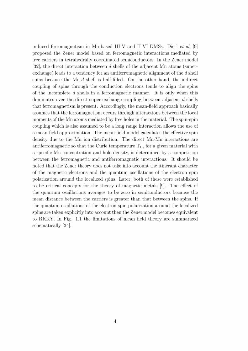
induced ferromagnetism in Mn-based III-V and II-VI DMSs. Dietl et al. [9]
proposed the Zener model based on ferromagnetic interactions mediated by
free carriers in tetrahedrally coordinated semiconductors. In the Zener model
[32], the direct interaction between 𝑑 shells of the adjacent Mn atoms (super-
exchange) leads to a tendency for an antiferromagnetic alignment of the 𝑑 shell
spins because the Mn-𝑑 shell is half-filled. On the other hand, the indirect
coupling of spins through the conduction electrons tends to align the spins
of the incomplete 𝑑 shells in a ferromagnetic manner. It is only when this
dominates over the direct super-exchange coupling between adjacent 𝑑 shells
that ferromagnetism is present. Accordingly, the mean-field approach basically
assumes that the ferromagnetism occurs through interactions between the local
moments of the Mn atoms mediated by free holes in the material. The spin-spin
coupling which is also assumed to be a long range interaction allows the use of
a mean-field approximation. The mean-field model calculates the effective spin
density due to the Mn ion distribution. The direct Mn-Mn interactions are
antiferromagnetic so that the Curie temperature TC, for a given material with
a specific Mn concentration and hole density, is determined by a competition
between the ferromagnetic and antiferromagnetic interactions. It should be
noted that the Zener theory does not take into account the itinerant character
of the magnetic electrons and the quantum oscillations of the electron spin
polarization around the localized spins. Later, both of these were established
to be critical concepts for the theory of magnetic metals [9]. The effect of
the quantum oscillations averages to be zero in semiconductors because the
mean distance between the carriers is greater than that between the spins. If
the quantum oscillations of the electron spin polarization around the localized
spins are taken explicitly into account then the Zener model becomes equivalent
to RKKY. In Fig. 1.1 the limitations of mean field theory are summarized
schematically [34].
4

Figure 1.1: A schematic phase diagram as a function of the exchange coupling
strength (abscissa) relative to the band Fermi energy (𝜖𝐹 ) and the carrier
concentration (ordinate) relative to the Mn concentration for carrier-induced
ferromagnetism in diluted magnetic semiconductors [34].
1.2.1.2 Bound magnetic polaron model
A drawback of the mean field Zener model is that charge carriers are treated
as free carriers. It does therefore not explain the experimentally observed
transport properties of insulating and ferromagnetic (GaMn)As, in particular
the observation of a Mott variable range hopping behavior at low temperatures
[37].The bound magnetic polaron (BMP) model is the opposite approach of
the mean field Zener model, which treats the carriers as quasi-localized states
in an impurity band. In this limit, a localized hole in (GaMn)As exhibits
antiferromagnetic exchange interaction with a number of magnetic impurities
within its localization radius, leading to the formation of a bound magnetic
bound polaron, illustrated in Fig. 1.2. In contrast to the antiferromagnetic
exchange interactions between the local spins and the holes leading to the
existence of BMP, the interaction between magnetic polarons is ferromagnetic.
Since the ratio of the exchange and thermal energy governs the effective radius
of the magnetic polaron, BMPs overlap at sufficiently low temperature. This
gives rise to a ferromagnetic exchange interaction between percolated BMPs
5

at low temperature. The disorder effects play a crucial role in the magnetic
properties [38] if the hole localization radius is less than the distance between
BMPs.
Figure 1.2: Interaction of two bound magnetic polarons (BMP). The shaded
region indicates overlap affected by fields from the two BMPs. The small and
large arrows show impurity and hole spins, respectively [37].
1.2.1.3 Donor impurity band model
The finding promising candidates for room temperature DMS, such as Mn-
doped 𝑝-ZnO and 𝑝-GaN, was of much interest in the scientific community
after the mean field Zener model prediction. Beside the above predicted can-
didates, several oxides such as TiO2, ZnO, SnO2, and In2O3 [24, 25, 27, 28]
have been reported to show room-temperature ferromagnetism. However, the
mean field Zener model predicted 𝑝 type DMS systems to be ferromagnetic,
while the reported materials are 𝑛-type, except for a few cases so a controversy
arises. Furthermore, many of the reported dilute magnetic oxides have Curie
temperatures above 300 K. Later, Coey et al. [10] suggested the donor impu-
rity band model to describe the properties of defect (e.g. oxygen vacancies)
derived 𝑛-type dilute magnetic oxides, which is the extension of the BMP the-
ory above described. Many oxides are 𝑛-type, due to oxygen vacancies, and
have a high dielectric constant. The main ingredients of the donor impurity
band model are as follows. Shallow donors associated with the defects form
6

BMPs, via which ferromagnetic ordering of magnetic moments of dopants is
mediated. The polarons overlap at a sufficiently high BMP concentration, thus
leading to a spin-split impurity band in the band gap and ferromagnetic order-
ing throughout the material. The ferromagnetic coupling between magnetic
ions via an impurity band is illustrated in Fig. 1.3 [10]. According to this
theory, if the donor electron resides in the vicinity of a magnetic impurity a
high Curie temperature is possible, even if the hybridization between the 3𝑑
levels and the conduction band states is just 1 ∼ 2 % [10]. There are two
possibilities for BMP formation by considering that the 3𝑑 levels of transition
metals in the series from Ti to Cu are below the conduction band. The first
occurs near the beginning of the 3𝑑 series, where the majority 3𝑑 level crosses
the Fermi level as shown in the impurity band in Fig. 1.3 (c), and the second is
towards the end of the 3𝑑 series where the minority 3𝑑 level crosses the Fermi
level as shown in Fig. 1.3 (b). This donor impurity band model relies on the
donor formation from defects, which however, are also favored sites of forming
metallic clusters. In addition, the weak 𝑠-𝑑 exchange interaction renders the
model rather impractical. The exchange interaction between band electrons
and the 3𝑑-electrons of the magnetic ions attributed to potential exchange and
kinetic exchange due to the hybridization. The potential exchange interaction
always exists which is induced by the repulsive Coulomb interaction between
the band and 𝑑-electrons. This process tends to align the spins of the band elec-
trons parallel to that of the dopant magnetic moments. The kinetic exchange
contribution stems from a reduction of kinetic energy by delocalization. The
kinetic exchange contribution is due to the hybridization of 3𝑑 levels with the
𝑠- and 𝑝-bands. At the Γ point, 𝑠-𝑑 hybridization is symmetry forbidden [39]
but 𝑝-𝑑 hybridization is always allowed, which may be a reason why 𝑝-type
materials are favored for DMS research. In summary, it is by now generally
accepted that the impurity band model cannot explain the Curie temperatures
above room temperature that have been observed in transition metal doped
magnetic oxides and nitrides [40]. In 𝑛-type DMS with Mn2+/3+ impurities
the exchange mechanism is rather close to the kinematic exchange proposed
by Zener for mixed-valence Mn ions [41].
7
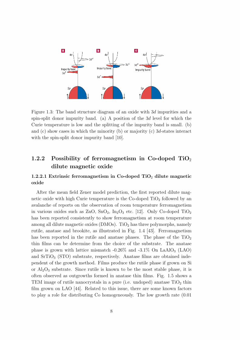
Figure 1.3: The band structure diagram of an oxide with 3𝑑 impurities and a
spin-split donor impurity band. (a) A position of the 3𝑑 level for which the
Curie temperature is low and the splitting of the impurity band is small. (b)
and (c) show cases in which the minority (b) or majority (c) 3𝑑-states interact
with the spin-split donor impurity band [10].
1.2.2 Possibility of ferromagnetism in Co-doped TiO2
dilute magnetic oxide
1.2.2.1 Extrinsic ferromagnetism in Co-doped TiO2 dilute magnetic
oxide
After the mean field Zener model prediction, the first reported dilute mag-
netic oxide with high Curie temperature is the Co-doped TiO2 followed by an
avalanche of reports on the observation of room temperature ferromagnetism
in various oxides such as ZnO, SnO2, In2O3 etc. [12]. Only Co-doped TiO2
has been reported consistently to show ferromagnetism at room temperature
among all dilute magnetic oxides (DMOs). TiO2 has three polymorphs, namely
rutile, anatase and brookite, as illustrated in Fig. 1.4 [43]. Ferromagnetism
has been reported in the rutile and anatase phases. The phase of the TiO2
thin films can be determine from the choice of the substrate. The anatase
phase is grown with lattice mismatch -0.26% and -3.1% On LaAlO3 (LAO)
and SrTiO3 (STO) substrate, respectively. Anatase films are obtained inde-
pendent of the growth method. Films produce the rutile phase if grown on Si
or Al2O3 substrate. Since rutile is known to be the most stable phase, it is
often observed as outgrowths formed in anatase thin films. Fig. 1.5 shows a
TEM image of rutile nanocrystals in a pure (i.e. undoped) anatase TiO2 thin
film grown on LAO [44]. Related to this issue, there are some known factors
to play a role for distributing Co homogeneously. The low growth rate (0.01
8

nm/s) in molecular beam epitaxy (MBE) leads to a layer-by-layer growth and
homogeneous Co distribution in the film as suggested by Chambers et al. [44].
In contrast, a higher rate (0.04 nm/s) leads to a large density of rutile phases
to which Co segregates above 823 K. Post-annealing is reported to result in
redistribution of Co atoms but also an increased clustering of Co within the
film [43]. Another possible factor for influencing the Co distribution could
be the oxygen vacancies. With decreasing oxygen pressure during growth, an
increasing tendency of Co to cluster is reported [43].
Figure 1.4: Structure of TiO2: (A) rutile, (B) anatase, and (C) brookite.
Initially, Chambers et al. [44] suggested carrier mediated ferromagnetism
in anatase Co-doped TiO2 thin films by showing that ferromagnetic behavior is
enhanced by increasing the carrier concentration. The anomalous Hall effects
(AHE) and magneto optical dichroism in rutile, and anatase Co-doped TiO2
also support carrier mediated ferromagnetism [45–48]. AHE is the well known
ferromagnetic response of carriers in ferromagnetic materials. In Fig. 1.6,
it is shown that rutile Co-doped TiO2 represents the anomalous Hall effect,
while its magnetic field dependence is similar to that of the magnetization
measured by magnetometry [49]. The AHE and magneto optical dichroism
measured by Toyosaki et al. [50] in rutile samples, and found a correlation
between them as a function of carrier concentration and external magnetic
field. These measurements suggest that carriers enhance the ferromagnetic
exchange interactions between isolated Co magnetic moments in Co-doped
TiO2.
9

Figure 1.5: Bright-field TEM image of 50-nm pure TiO2 at LaAlO3(001) sub-
strate. Rutile nanocrystals are indicated by R1 and R2 [44].
Figure 1.6: For rutile Co-doped TiO2, the magnetic field dependence of the
Hall resistivity at 300 K. The inset figure is the magnetic field dependence of
the magnetization for the same sample at 300 K [49].
Shinde et al. [51] suggested, that observing an AHE is not a robust test for
confirming carrier mediated ferromagnetism because the co-occurrence of super
10

Figure 1.7: XMCD spectra of anatase Co-doped TiO2 for different post an-
nealing times in comparison with those of Co metal: 0 (as grown), 2, 10, and
20 min. (a) Co 𝐿2,3-edge XAS spectra (Co 10%) (b) Co 𝐿2,3-edge XAS spec-
tra recorded with right- and left circular polarization (Co 10%) (c) Resulting
difference spectra that is, X-ray magnetic circular dichroism (XMCD).
Figure 1.8: For a rutile Co-doped TiO2 thin film (3% Co) (a) Co 𝐿3-edge region
with right- and left circular polarization. (b) Co 𝐿3-edge XMCD. Alleged
multiplet features are denoted by arrows [53].
11

paramagnetic Co clusters and the AHE is possible in Co-doped TiO2 films.
Since XMCD is a useful probe since it reflects element specific contributions
to magnetism so Kim et al. [52] investigated the origin of ferromagnetism of
anatase Co-doped TiO2 with x-ray absorption spectroscopy (XAS) and x-ray
magnetic circular dichroism (XMCD). They found that the ionic multiplet
structure of the Co 𝐿-edge is smeared out gradually with increasing annealing
time, and finally the spectral shape becomes identical to that of Co metal,
suggesting that Co metal clusters are the cause for ferromagnetism as shown in
Fig. 1.7 (a), In Fig. 1.7 (c), the weak XMCD signal increases with annealing
time at 400∘C, indicating that most Co is segregated during the annealing
process. In contrast, Mamiya et al. [53] reported multiplet features in Co 𝐿-
edge XMCD spectra in Fig. 1.8, suggesting that Co2+ ions, and not metallic
Co which is characterized by featureless spectra, contribute to magnetism.
1.2.2.2 Intrinsic ferromagnetism in Co-doped TiO2 dilute magnetic
oxide
Several theories proposed to explain the origin of room temperature ferro-
magnetism in dilute magnetic oxides. However, the local spin density approx-
imation (LSDA) is well known to overestimate the 𝑠𝑝-𝑑 hybridization and the
energy of the transition metal 3𝑑 level relative to the band edges, due to the
underestimation of the band gap. Consequently, this approach leads to a lot
of conflicting results in DMS studies [2, 10]. Coey et al. [10] proposed an im-
purity band model which may be a possible explanation for carrier mediated
magnetism, but a recent calculation shows that oxygen vacancies in oxides
induce deep levels, and cannot lead to long range ferromagnetic exchange in-
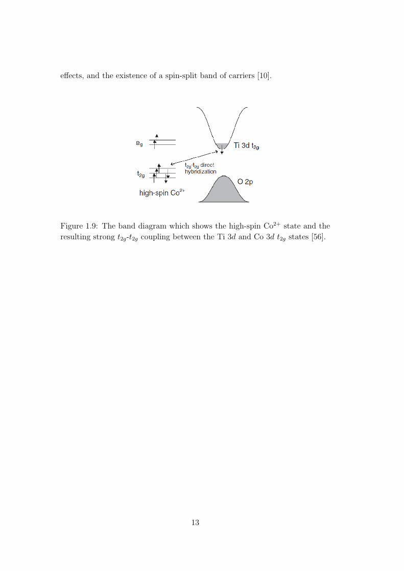
teraction [54, 55]. Quilty et al. [56] suggested a strong hybridization between
the conduction band and 𝑡2𝑔-states of a high spin Co2+ ion in rutile Co-doped
TiO2,. The direct 𝑑 − 𝑑 hybridization as illustrated in Fig. 1.9. by X-ray
photoelectron spectroscopy (XPS) measurements showed that Co2+ is with
high-spin state in which an unoccupied 𝑡2𝑔 state is expected to hybridize with
the Ti 3𝑑 𝑡2𝑔 derived conduction band. The authors observed a shift of the
conduction band, which may be expected due to its exchange splitting with
increasing Co doping up to 10%.
For proving intrinsic DMS behavior, carrier-mediated ferromagnetism
such as tunable ferromagnetism and control of magnetization direction by elec-
tric fields should be demonstrated, along with the measurement of AHE. So far,
these have not yet been demonstrated and the mystery the origin of magnetism
in dilute magnetic oxides still remains. If the reported room-temperature di-
lute magnetic oxides are real DMS, they should show electric tunability of fer-
romagnetism, large tunnel magnetoresistance effects, strong magneto-optical
12
effects, and the existence of a spin-split band of carriers [10].
Figure 1.9: The band diagram which shows the high-spin Co2+ state and the
resulting strong 𝑡2𝑔-𝑡2𝑔 coupling between the Ti 3𝑑 and Co 3𝑑 𝑡2𝑔 states [56].
13

1.3 Multiferroics
1.3.1 Multiferroic materials and magnetoelectric effect
Multiferroics are materials in which at least two of the ferroelectric, ferro/anti
ferromagnetic and ferroelastic phases coexist. Though the mechanisms that
allow ferroelectricity and ferromagnetism seem to be incompatible, there are
a select few materials in which ferroelectricity and ferromagnetism are both
present, namely BiFeO3, Cr2O3, yttrium- iron-garnets, boracites, rare-earth
ferrites and manganese-based perovskites. In these materials, the ferroelectric
and ferro/antiferromagnetic phases are coupled in such as way as to produce
a cross phenomenon known as the magnetoelectric (ME) effect. This allows
manipulation of the magnetic phase with an external electric field and/or ma-
nipulation of the electric phase with external magnetic field. The integration
of the ME effect into device technology would have substantial implications,
however the above mentioned single phase materials exhibit prohibitively small
ME effect [57, 58].
1.3.2 Single phase multiferroic materials: a brief history
[59]
Nickel iodine boracites, Ni3B7O13I were discovered as first ferromagnetic
ferroelectric material. Many more multiferroic boracites compounds were syn-
thesized by the above compound, these compounds have complex structures
with many atoms per formula unit and more than one formula unit per unit
cell. The isolation can be prevented in these materials by the large number of
inter-ionic interactions, both of the essential factors causing multiferroism and
of the nature of the coupling between the magnetic, electric, and structural
order parameters. Nickel iodine boracites can be thought of as the “Rochelle-
salt” of magnetic ferroelectrics. It has wide applicability or to contribute to
our increased understanding in the field.
Other Perovskites: A number of other perovskites are known to have
ferroelectric and magnetic (mostly of the Antiferromagnetic type) ordering.
These include the manganites of the small rare earth elements and yttrium
and a few compounds in which Bi is the large cation. Table 1.2 lists some of
the known Multiferroic materials adapted from [58]
1.3.3 Multiferroic composites
There is only few number of single-phase materials which exhibit the coexis-
tence of strong ferro/ferrimagnetism and ferroelectricity at room temperature.
14

Table 1.2: Examples of materials that exhibit ME effect. Nota-
tion: FE-Ferroelectric, AFE-Antiferroelectric, FM-Ferromagnetic, AFM-
Antiferromagnetic and WFM-weak Ferromagnetic [58].
Compound Type of electric order Type of magnetic order TC (K) TN (K)
Pb(Fe2/3W1/3)O3 FE AFM 178 363
Pb(Fe1/2Nb1/2)O3 FE AFM 387 143
Pb(Co1/2W1/2)O3 FE WFM 68 9
Pb(Mn2/3W1/3)O3 AFE? AFM 473 203
Pb(Fe1/2Ta1/2)O3 FE AFM 233 180
Eu1/2Ba1/2TiO3 FE FM 165 4.2
BiFeO3 FE AFM 1123 650
BiMnO3 AFE FM 773 103
YMnO3 FE AFM 913 80
YbMnO3 FE AFM/WFM 983 87.3
HoMnO3 FE AFM/WFM 873 76
ErMnO3 FE AFM 833 79
Ni3B7O13I FE WFM 64 64
Ni3B7O13Br FE WFM 398 30,40
Co3B7O13I FE WFM 197 38
Van Suchtelen et al. [60] proposed that composites of piezoelectric and mag-
netostrictive phases can be electromagnetically coupled via stress mediation
.
1.3.4 Magnetoelectric effects
The coupling between magnetic and electric properties of a material gives rise
to magneto-electric effects. The Magnetoelectric (ME) effects were very popu-
lar in the beginning of 19th century after their discovery by Curie and Rontgen.
However, the progress understanding ME effects seems to have stopped since
about 1970 because of the lack of materials and degrees of freedom to modify
these effects.
BiFeO3 (BFO) is the only single phase material which shows simulta-
neously ferroelectric and ferromagnetic properties at room temperature. BFO
was first synthesized by Royen and Swars. Various studies have been done to
15

this compound, mostly on ceramics motivated by the potential high magneto-
electric property. However, for many researchers it was the matter of contro-
versies to discuss relationship between the structural and physical properties
of BFO.
1.3.5 Physical properties of BiFeO3
1.3.5.1 Structural Properties of BiFeO3
The structure of BFO is characterized by two distorted perovskite unit cells
(a𝑟 = 3.96 A, 𝛼𝑟 = 0.6∘) connected along their body diagonal, denoted by
the pseudocubic < 111 >, to form a rhombohedral unit cell as shown in Fig.
1.10 (a) [61, 62]. The ferroelectric state is realized by a large displacement
of the Bi ions relative to the FeO6 octahedra. This structure results in two
important considerations. First, the ferroelectric polarization lies along the
pseudocubic < 111 > leading to the formation of eight possible polarization
variants, corresponding to four structural variants [63, 64]. Second, the anti-
ferromagnetic ordering of BFO is G-type, in which the Fe magnetic moments
are aligned ferromagnetically within the(111) plane and antiferromagnneti-
cally between adjacent (111) plane. Additionally, BFO is known to exhibit
a spin cycloid structure in the bulk [64] and the preferred orientation of the
antiferromagnnetically aligned spins lies within the (111) plane, perpendicular
to the ferroelectric polarization direction with six equivalent easy axes within
that plane. The magnitude of the ionic shifts are Bi: 0.62Aalong [111], Fe:
0.23Aalong [111], O: 0.30Aalong [111] (all values ± 0.03A). The nature of the
oxygen shifts is more easily visualized by considering the atomic positions and
shifts on a (111) rhombohedral plane. It is seen that the oxygen shifts are
essentially along a line between the projections of two Bi atoms on this plane.
In the ideal perovskite structure, Bi atoms would lie in this (111) plane, but
in BFO Bi shifts by 0.62Anormal to the plane.
The unit cell of BFO is not the unit molecular cell as shown in Fig. 1.10
(b), but may be represented by a rhombohedron, having twice the volume of
the unit molecular cell, and generated by taking three face diagonals meeting
at a vertex of the cube shown as three intersecting edges of the rhombohedron.
16
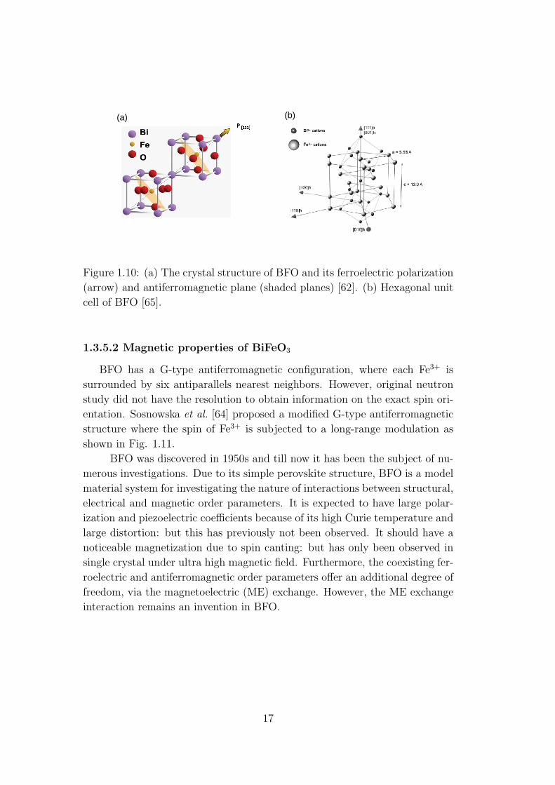
(a) (b)
Figure 1.10: (a) The crystal structure of BFO and its ferroelectric polarization
(arrow) and antiferromagnetic plane (shaded planes) [62]. (b) Hexagonal unit
cell of BFO [65].
1.3.5.2 Magnetic properties of BiFeO3
BFO has a G-type antiferromagnetic configuration, where each Fe3+ is
surrounded by six antiparallels nearest neighbors. However, original neutron
study did not have the resolution to obtain information on the exact spin ori-
entation. Sosnowska et al. [64] proposed a modified G-type antiferromagnetic
structure where the spin of Fe3+ is subjected to a long-range modulation as
shown in Fig. 1.11.
BFO was discovered in 1950s and till now it has been the subject of nu-
merous investigations. Due to its simple perovskite structure, BFO is a model
material system for investigating the nature of interactions between structural,
electrical and magnetic order parameters. It is expected to have large polar-
ization and piezoelectric coefficients because of its high Curie temperature and
large distortion: but this has previously not been observed. It should have a
noticeable magnetization due to spin canting: but has only been observed in
single crystal under ultra high magnetic field. Furthermore, the coexisting fer-
roelectric and antiferromagnetic order parameters offer an additional degree of
freedom, via the magnetoelectric (ME) exchange. However, the ME exchange
interaction remains an invention in BFO.
17

Figure 1.11: Portion of the BFO lattice and the arrows indicate the Fe3+
moment direction of the proposed model. The spiral period is reduced for
illustration purpose. Figure is taken from Sosnowska et al. [64].
1.3.5.3 Electrical properties of BiFeO3
Due to the low resistivity of samples the electrical characterization on bulk
BFO has been very difficult. The controversy about whether it is ferroelectric
or antiferroelectric was finally settled based on the hysteresis loop measured
by Teague et al. [66]. He performed an experiment in liquid nitrogen which
shows lower leakage current due to lower charge carrier density and mobility.
The measured spontaneous polarization was 3.5 𝜇C/cm2 along the < 100 >
direction, which represents 6.1 𝜇C/cm2 in the < 111 > direction. This value
is much smaller than what would be expected for a ferroelectric material.
The leakage problem, likely due to defects and non-stoichiometry, has been
hampering more comprehensive studies about the bulk BFO and has limited
applications of this material. To solve this problem, recent work has focused
on solid solutions of BFO with other ABO3 materials, such as BaTiO3, which
can prevent second phase formation and increase sample resistivity. For ex-
ample, Ueda et al. have reported a remnant polarization of 2.5 𝜇C/cm2 from
(Bi0.7Ba0.3)(Fe0.7Ti0.3)O3 film [67–69]. The various measured values for the
18

polarization in BFO are summarized in following table-
Table 1.3: The values for the polarization in BiFeO3 is taken from litrature,
in chronological order with the oldest at the top.P [𝜇C/cm2] Sample type Ref.
6.1 Bulk single crystals [66]
2.5 (Bi0.7Ba0.3)(Fe0.7Ti0.3)O3 films (300 nm) on Nb-doped SrTiO3 [67]
2.2 Polycrystalline films (200 nm) [70]
50-90 Thin films (400-100 nm) on SrRuO3 /SrTiO3 [68]
35.7 Polycrystalline films (350 nm) [71]
8.9 Bulk ceramics [72]
158 Polycrystalline films (300 nm) [73]
The controversies concerning BFO can be summarized as follows-
(1) Due to the samples high conductivity, electrical characterization of
bulk single crystal/ceramics has been difficult. The spontaneous polarization
value measured Teague et al. [66] is much smaller than what would be expected
for a ferroelectric material with such a high Curie temperature and large dis-
tortion. Later, scientists tried to mix other ABO3 materials into BFO forming
solid solutions; this helps to increase the sample resistivity. Ueda et al [67]
reported a P𝑟 of ∼ 2.5 𝜇C/cm2 from BFO/BaTiO3 thin films. More recently,
BFO thin films with high resistivity have also been made [74].
(2) Early neutron diffraction study revealed a 𝐺-type antiferromagnetic
spin order for BFO with a small canting between neighboring antiparallel Fe3+
ions [70]. It was concluded that BFO should show weak ferromagnetic prop-
erty at room temperature. But no such behavior has been reported. Later,
Sosnowska et al. [64, 70] reported that the antiferromagnetic order of BFO is
subjected to a spiral modulation that cancels out the net magnetization. By
breaking this cycloidal structure, one could release the magnetization due to
canting [75,76].
1.3.6 Substitution studies of transition-metal ions in BiFeO3
As we know that BFO is a ferroelectric and an antiferromagnet with spa-
tially modulated spin structure. This structure does not allow net magneti-
zation and inhibits the observation of a notable linear magnetoelectric effect.
This problem can be solved by substitution of Fe3+ by other transition-metal
ions. Unfortunately, 𝐵-site ion doping decreases magnetic ordering temper-
ature drastically [77]. Moreover, a high pressure synthesis is necessary to
prepare the ceramic samples [77]. An alternative way to induce a net mag-
19

netization in the BFO is a rare-earth (RE) substitution in the 𝐴 sublattice
of the ABO3 structure. Gd3+, Tb3+, etc., possess a large magnetic moment,
causing significant increase in magnetization even in the lightly doped com-
pounds. More recently, enhancement of magnetization has been reported in
Bi1−𝑥RE𝑥FeO3 (RE=Nd3+,Sm3+), materials [78, 79]. Moreover, the appear-
ance of net magnetization has been observed in La3+ and Ba2+-doped samples
(i.e., under diamagnetic doping) [80, 81]. It has been suggested that the sub-
stitution suppresses an incommensurate spin configuration and causes a small
spin canting [82].
In addition to studies on pure BFO, doping of BFO with a foreign atom
at either 𝐴- or 𝐵-site of the perovskite (ABO3) structured BFO lattice, has
been shown to play an important role in altering its properties. For exam-
ple, substitution of Bi, the bigger 𝐴-site cation, with lanthanide elements such
as lanthanum (La), neodymium (Nd) has been shown to result in remark-
able improvement of the properties of BFO thin films although results varied
from one group to another. On the other hand, Fe, smaller 𝐵-site cation,
has been substituted by elements such as Cr which resulted in an increase
in the polarization but also led to substantial increase in the coercive field.
By using smaller Nd3+ ions (radius=0.983A) in substitution for larger Bi3+
ions (radius=1.03A) in the BFO composition, it is possible to create single-
phase multiferroic Bi1−𝑥Nd𝑥FeO3 (𝑥=0-0.15) ceramics possessing an improved
spatial uniformity of magnetic structure, and a rather linear ferromagneto-
electric behavior [78, 83]. Compared with La3+ ion (radius=1.032A), Sm3+
ion (radius=0.958A) possesses a much smaller radius. This suggests that the
effect of 𝐴-site substitution may further be enhanced if Sm3+ ion is used in
substitution for Bi3+ ion (radius=1.030A) in the ordinary BFO composition.
In Bi1−𝑥Sm𝑥FeO3 system, residual magnetization (M𝑟) may be enhanced by
increasing the 𝐴-site Sm substitution. These modifications in the functional
properties are expected to occur due to the changes in the electronic or crys-
tal structure of BFO, as reported previously for bulk BFO [85]. Nakamura et
al. [84] studied the effect of Co-doping, using a reasonably large range (up to
30 atom%) as compared to previous reports [85–88], on the structural prop-
erties of BFO thin films on LaAlO3 (001) substrate synthesized by chemical
solution deposition and here they report on the structural changes observed
in the BFO thin films induced by Co doping on 𝐵-site which also affected the
electrical and magnetic behavior of these films. To minimize the substrate
induced texture effects, we employed SrRuO3 for growing epitaxial thin films
of BFO which also serves as a base electrode.
20

1.4 Heusler Alloys
The Heusler compounds have a very old story regarding magnetism, starting
more than 100 years ago with the invention of the ternary metallic compound
Cu2MnAl by A. Heusler in 1903 [89]. Remarkably, without none of its elements
is ferromagnetic even though this alloy is a ferromagnet. Further investigations
showed that the general composition 𝑋2𝑌 𝑍 exists as a class of isostructural
ternary metallic alloys, where 𝑋 denotes a transition metal element such as
Ni, Co, Fe or Pt, 𝑌 is a second transition metal element, e.g., Mn, Cr or Ti
and 𝑍 is an atom from 3rd, 4th or 5th group of the periodic table such as Al,
Ge, Sn or Sb. More than thousands different Heusler compounds have been
synthesized until now, a widespread evaluation of experimental work until the
year 1987 can be found in Ref [90]. Due to their very versatile magnetism
Heusler compounds have attracted considerable amount of interest. Actually
the Heusler compound is the predicted half-metallic ferromagnetic nature for
some of these alloys which is the driving force for the intense study of these
alloys [91–95]. Half-metals can be considered as hybrids between metals and
semiconductors since we know that Half-metals are ferromagnetic materials.
The Heusler compounds possess a wide energy gap for minority spin direction
at the Fermi level (𝐸𝐹 ) which give a complete spin polarization at 𝐸𝐹 . This
makes them ideal candidates for applications in spintronics.
This chapter gives a short review of structural, magnetic and elec-
tronic properties of the Heusler compounds in general with emphasis on the
half-metallic Heusler alloys, especially the Co-based ones, since Co2MnSi and
Co2MnGe are the alloys studied in this thesis. After the basic properties of
the bulk Heusler compounds are discussed, some of the recent results and open
problems are presented.
1.4.1 Physical properties of Heusler alloys
1.4.1.1 Structural Properties of Heusler alloys
Heusler alloys are ternary intermetallic compounds. At the stoichiometric
composition, the full Heusler alloys 𝑋2𝑌 𝑍 and the half Heusler 𝑋𝑌 𝑍 struc-
tures are 𝐿21 and 𝐶1𝑏, respectively. The 𝑋 and 𝑌 elements are magnetic
elements; the atom 𝑍 is non-magnetic element. The unit cell have four inter-
penetrating fcc sublattices at (000) and (1/2, 1/2, 1/2) for 𝑋, (1/4, 1/4, 1/4)
for 𝑌 and (3/4,3/4,3/4) for 𝑍 atom. For half-Heusler compounds the site (1/2,
1/2, 1/2) is empty. The two structures are closely related with vacant sites.
The 𝐶1𝑏 structure can be obtained from the 𝐿21 one by replacing the half of
the 𝑋 sites in an ordered manner as shown in Fig 1.12.
21

Figure 1.12: Crystal structures of Heusler alloys (a) 𝐿21 full-Heusler and (b)
𝐶1𝑏 half-Heusler ordered structures. The structure consists of 4 interpene-
trating fcc lattices. One of the four sub lattices is empty in the case of the
half-Heusler alloys. Disordered Heusler phases: (c) 𝐵2 disorder due to the
𝑌 -𝑍 exchange and (d) 𝐴2 disorder caused by the 𝑋-𝑍 or 𝑋-𝑌 intermixing.
One notices that if all atoms are identical, the lattice is simply bcc.
The Heusler compounds are the low temperature equilibrium phase for
the ordered 𝐿21 structure. In the majority of Heusler alloy like the original
Heusler phase Cu2MnAl there exist several structural modifications with dif-
ferent degree of site disorder of the atoms on the 𝑋, 𝑌 and 𝑍 sites. At high
temperatures the crystal structure of Heusler compound is bcc with random
occupation of the atoms on the lattice sites of a simple bcc lattice with half
of the lattice parameter compared to the 𝐿21 structure. For the Heusler com-
pounds, an intermediate structure with 𝐵2 symmetry often occurs. 𝐵2 has
the same lattice parameter as the 𝐿21 phase, but the distribution of 𝑌 and
𝑍 atoms are random on the corresponding sublattices, whereas the two 𝑋
sublattices remain intact.
22

1.4.1.2 Magnetic properties of Heusler alloys
Heusler alloys possess attractive magnetic properties because it is very in-
teresting materials. Anyone can study in the same family of alloys a series
of interesting diverse magnetic phenomena like itinerant and localized mag-
netism, antiferromagnetism, heavy-fermion behavior, helimagnetism and Pauli
paramagnetism [96–99].
The majority of Heusler alloys with a magnetic element at the 𝑌 site
order ferromagnetically, on the other hand, a number of antiferromagnetic
compounds also exist, e.g. Ni2MnAl or Pd2MnAl [100, 101]. The major in-
put to the magnetic moments in the Heusler phases usually stems from the
atoms at the 𝑌 site. If the 𝑋 sites are also occupy by the magnetic atoms,
their moment is usually quite small or even vanishing. For example the Ni
atoms are non-magnetic as mentioned in the above Ni2MnAl compound. A
few Heusler compound with rather large magnetic moments both on the 𝑋
and the 𝑌 sites are also exist. For such case the ferromagnetic Curie tem-
perature 𝑇C becomes exceptionally high and the ferromagnetic state is very
stable. The best examples which show the Co moment of about 1 𝜇𝐵 and the
Curie temperature of 985 K [102] and 1100 K [103] are provided by the Heusler
phases Co2MnSi and Co2FeSi, respectively, the highest 𝑇C values known for the
Heusler alloys. The mechanism which stabilizes the ferromagnetism is a strong
next-nearest neighbor ferromagnetic exchange interaction between the spins at
the 𝑋 and the 𝑌 site [91, 104]. If a non-magnetic element is at 𝑋 site, the
leading exchange interaction between the 𝑌 spins is of weaker super-exchange
type due to hybridization, mediated by the electrons of the non-magnetic 𝑍
atoms. Depending on the valence of 𝑍 the magnetic interaction can have either
sign [104].
Table 1.4: From generalized gradient approximation (GGA) lattice constant,
total spin moment and predicted spin magnetic moments of Co2MnGe are
calculated and their experiment values, taken from Ref. [94].
a[nm] 𝜇tot[𝜇𝐵] 𝜇Mn[𝜇𝐵] 𝜇Co[𝜇𝐵] 𝜇Ge[𝜇𝐵]
experiment 0.574 [101] 5.11 - - -
theory 0.574 5.0 2.98 1.02 -0.03
In Table 1.4, the spin magnetic moments for Co2MnGe are listed. It
possess a spin moment of ∼ 1.0 𝜇𝐵 because the Co atoms are ferromagnetically
coupled to the Mn spin moments and. The Ge atoms have orbital hybridization
which is two orders of magnitude smaller than the Co moment and hence it
has a very small negative moment. The orbital moments absolute values are
23

negligible with respect to the spin magnetic moments [94, 105] because they
are completely quenched.
Heusler compounds such as Cu2MnAl with a magnetic moment only on
the 𝑌 site are considered as good examples of localized 3𝑑 metallic magnetism.
Since there are no Mn-Mn nearest neighbors in the ideal 𝐿21 structure, the
magnetic moments remain essentially localized at the Mn position and the
Mn 3𝑑 wave functions overlap only weakly. However, the magnetic moments
only on the 𝑋 sites for the compound Co2TiSn exhibits weak itinerant ferro-
magnetism with strongly delocalized magnetic moments [106]. As it is clear
from the crystallographic structure as shown in Fig 1.12, the overlapping of
the nearest neighbor X atoms are making of the 3𝑑 wave functions and the
delocalized character of the 𝑑 electrons much larger than in the case of only
the atoms at the 𝑌 site being magnetic. By replacing the Co atoms to Ni
in Co2TiSn, this delocalization effect proceeds further, making the compound
Ni2TiSn a Pauli paramagnet [107].
1.4.1.3 Electronic properties of Heusler alloys
By electron energy-band calculations the spectacular property of full spin
polarization at the Fermi level 𝐸𝐹 was first predicted in 1983 for the NiMnSb
[108]. It have been predicted that PtMnSb and CoMnSb posses this property.
NiMnSb, PtMnSb and CoMnSb have been half-metals [108], since only for ma-
jority spin there is metallic conductivity and for the minority spin the conduc-
tivity is of semiconducting type. In a ferromagnetic transition metal alloys, this
half-metallicity is a very rare property, since usually 𝑠 or 𝑝 bands with a small
exchange splitting cross the Fermi energy and contribute states of both spin
directions. The half-Heusler alloys PtMnSb, NiMnSb and CoMnSb remained
the only ferromagnetic alloys with half-metallic character for several years.
The half-metallic Heusler alloys, Co2MnSi, Co2MnGe and Co2Mn(Sb𝑥Sn1−𝑥)
was found theoretically in the starting of 1990 [93, 109, 110]. The calculated
indirect band gap for the minority carriers is smaller in these materials than
in the half-Heusler compounds [105], for Co2MnSi and Co2MnGe one derives
𝐸gap=0.81eV and 𝐸gap=0.54 eV, respectively. This spin-projected density of
states for Co2MnGe is shown in Picozzi et al. [94].
The origin of the gap in the minority spin band is quite subtle, how-
ever recently band-structure calculations allowed to disclose the fundamental
mechanism for the formation of the gap. The 𝑑− 𝑑 hybridization between the
transition atoms composing Heusler alloys is essential for the formation of the
gap at 𝐸𝐹 . The gap in the case of half-Heusler compounds (e.g., NiMnSb) is
created by the hybridization and bonding-antibonding splitting between the
Mn 𝑑 and the Ni 𝑑 states. However, the gap in the case of full Heusler al-
24

loys (e.g., Co2MnGe) originates from the hybridization between the 𝑑 states
of the two Co atoms and subsequent interaction of these hybrids with the Mn
𝑑 states [91].
The experimental proof of these Heusler alloys is a long and still on-
going controversial issue for the half-metallicity. The electron transport mea-
surement to test the existence of a gap in the spin down electron band was
the first attempts to prove the half-metallicity [111, 112]. Since in the half-
metal for temperatures small compared to the gap in the minority spin band
there is only one spin direction at the Fermi level available, it is expected
that electronic scattering processes involving spin flips and longitudinal spin
wave excitations are inhibited. Thus one should suppose increasing electron
mobility and a change of power law describing the temperature dependence
of the resistivity, when the gap for the minority spin band becomes larger
than the thermal energy. Actually such type of behavior for temperatures
below 80 K has been detected for NiMnSb compound. Additionally the Hall
coefficient shows an anomalous temperature dependence in this temperature
range, strongly suggesting across a gap a thermal excitation of charge car-
riers coexisting with metallic conductivity [111, 112]. Finally, by analyzing
the current-voltage (𝐼 − 𝑉 ) characteristic below the superconducting gap of
a point contact between a Nb superconductor and a bulk PtMnSb sample,
which is dominated by Andreev reflections at the ferromagnet/superconductor
interface, spin polarization of 90% at the Fermi level derived [113].
The spin polarized neutron diffraction measurements on the Co2Mn(Si,
Ge, Sn) samples have been employed to determine the degree of spin polariza-
tion at the Fermi level [114]. This methods probe the spatial distribution of
the magnetization and so it depend sensitively on the spin polarization. The
results imply a finite density of states in the minority spin 𝑑 band of man-
ganese. Hence the spin polarization approaches to larger value, but not 100%.
Recently superconducting/ferromagnetic measurements on a Co2MnSi single
crystal gave a spin polarization of 55% [115]. Similarly, the degree of spin
polarization determined from spin resolved photoemission spectra and it was
always found to be definitely below 100% [116,117].
During the first years after the discovery of the half-metallic character
in the Heusler compounds were considered as exotic ferromagnets for mainly
academic interest. With the development of new ideas of data storage and pro-
cessing designed the attitude have changed completely to use both the charge
and the spin degree of freedom of the conduction electrons, currently call spin-
tronics [118–120]. The non-volatility, increased processing speed and decreased
electric power consumption these are advantages by adding the spin degree of
freedom to conventional electronic devices in these alloys [118, 121]. There is
25

a strong belief in the spintronics community that in future these new concepts
have the perspective to complement or even substitute conventional Si tech-
nology. How valuable it would be for spintronic devices was rapidly realized by
spintronics community to have a ferromagnet available with only one conduc-
tion electron spin direction at the Fermi level. With an electrode possessing
100% spin polarization, the generation of a fully polarized current for spin
injection into semiconductors would be possible [122] and in metallic thin film
systems spin filtering and spin accumulation would be most effective [123]. The
giant magnetoresistance (GMR) [124] as well as the tunneling magnetoresis-
tance (TMR) [125] of a device prepared of two half-metallic electrodes should
be high, since electrical current for one spin direction is totally blocked to first
order, if the two electrodes have opposite magnetization directions.
The novel concepts of spintronics started an upsurge of interest in fer-
romagnetic half-metals in the literature. In addition the half and full Heusler
alloys, there are some binary oxides (e.g., CrO2 and Fe3O4) [113], manganites
(e.g. La0.7Sr0.3MnO3) [113], transition metal chalcogenides (e.g., CrSe) and
pnictides (e.g., CrAS) in the zinc-blende or wurtzite structures [126], diluted
magnetic semiconductors (e.g. GaAs and ZnO doped with magnetic transition
metal ions) [127,128], and the fully spin polarized Heusler alloys.
For several technical reasons and/ or applications the Heusler alloys
seems to be very attractive. Their crystal structure and lattice constant are
closely related to the diamond and zinc-blende structures of most industri-
ally relevant semiconductors and the lattice mismatch is low, for instance for
Co2MnSi with GaAs it is less than 0.4% [129]. The preparation of Heusler
thin films are compatible with current semiconductor technology and can be
carried out by conventional metal film preparation methods. An additional
advantage of these alloys is their high ferromagnetic Curie temperatures, even
at 300 K the half-metallic Heusler alloys are close to ferromagnetic satura-
tion. This is of particular importance, since the temperature dependence of
the spin polarization scales with the corresponding magnetic moment of the
material [130].
Recent deep theoretical investigations using electronic energy band struc-
ture calculations increased the number of Heusler compounds with predicted
half-metallic properties to more than 20, among them Co2CrAl, Fe2MnSi,
Co2CrAl, Co2Cr0.6Fe0.4Al, and Co2FeSi, to mention a few of the new com-
pounds [91, 92]. The experimental work in the literature mostly has been in-
tensed on the classical Heusler half-metallic phases NiMnSb and PtMnSb, the
alloys Co2MnSi and Co2MnGe and the recently exposed compound Co2(CrFe)Al
[131], leaving a huge field for advance experimental investigations.
However, as already stated above the half-metallicity of the Heusler
26

compounds is a subtle property which is easily lost in a real sample.
1.4.2 Heusler half-metals in devices
Its promising application in spintronic devices is the main motivation be-
hind the experimental research on the fully spin polarized Heusler compounds.
Among the most promising materials to be integrated into technologically rel-
evant magnetic tunnel junctions (MTJs) as magnetic electrodes are the half-
metallic Heusler alloys. The effective amplitude of the magnetoresistance in a
simple layered system, consisting of two ferromagnetic metals, separated by a
thin insulating layer, which serves as a tunnel barrier [133], can be expressed
as:
TMR= 𝑅𝐴-𝑅𝑃/𝑅𝑅= 2𝑃1𝑃2/1-𝑃1𝑃2,
where 𝑅𝐴 and 𝑅𝑃 represent the resistance of the two ferromagnetic layers
with their magnetizations aligned antiparallel or parallel to each others and
𝑃1 and 𝑃2 are the spin polarizations at the Fermi level for electrodes 1 and 2,
respectively. Thus, by employing high spin polarized ferromagnetic electrodes
on both side of MTJ, high TMR values can be achieved.
Thin films of Heusler compounds are obviously needed but bulk samples
are not very useful. However, thin film preparation in general, especially thin
film heterostructures preparation, often imposes limits on the process param-
eters and this might severely interfere with the needs to have a high degree of
spin polarization. In order to obtain a large spin polarization, it is important to
have a perfect crystal structure with a small number of grain boundaries. This
can be best achieved by keeping the substrate at high temperature during the
thin film deposition. However, at high temperatures, most Heusler phases grow
in the Vollmer-Weber mode (three-dimensional islands), thus there might be a
strong roughening of the surfaces when using high preparation temperatures,
which for spintronic devices should be avoided. Furthermore, high preparation
temperatures are forbidden in thin film heterostructures combining different
metallic, semiconducting or insulating layers with the Heusler compounds to
avoid excessive inter-diffusion at the interfaces.
TMR devices and thin films was first investigated systematically using
the half-Heusler compounds PtMnSb and NiMnSb [133, 134]. The result was,
however, not encouraging. The spin polarization of NiMnSb integrated in a
MTJ was measured to be 25% at 4.2 K corresponding to a TMR amplitude
of 19.5% [134]. At room temperature the TMR value was 9%. Later, it was
found that Co2MnSi- and Co2MnGe-based TMR devices have shown much
better performance. For tunnel junctions of textured Co2MnSi with an Al
oxide tunnel barrier, a maximum TMR ratio of 108% at 20 K and 33% at room
27

temperature was achieved, corresponding to 72% and 41% of spin polarization,
respectively [135–137]. Recently, Yamamoto et al. [138] used high quality
epitaxially grown Co2MnSi electrodes and they were able to obtain a further
improvement to 1135% (92% spin polarization) at 4.2 K and 236% at room-
temperature. This is actually the highest TMR value observed for junction
using a MgO tunnel barrier. MTJs using a Co2MnGe electrode were recently
developed by the same group. The epitaxial tunnel junctions using MgO as
tunneling barrier showed strongly temperature dependent characteristics with
TMR ratios of 220% at room temperature and 650% at 4.2 K. For the newly
predicted half-metal Co2Cr0.6Fe0.4Al as a magnetic electrode using a MgO
tunneling barrier, a TMR ratio of 74% at 55 K was found [139–141]. The
maximum TMR value obtained for an Al oxide barrier are 52% and 83% at
5 K [142]. The spin polarization was found to be 81% [143]. Among the
MTJs with an amorphous Al oxide tunnel barrier, MTJ with the 𝐵2 ordered
Co2MnAl obtained a large TMR ratio of 83% at 2 K suggesting that one 𝐵2
ordered Co2MnAl may exhibit a high spin polarization [144]. In junctions
using a Co2FeSi electrode, smaller values for the TMR ratio were obtained, i.e.
41% at room temperature and 60% at 5 K.
Regarding the GMR effect in antiferromagnnetically coupled metallic
multilayers or in spin valves consisting of Heusler compounds, only a few ex-
periments have been performed. Current-in-plane (CIP) GMR effect at room
temperature has been measured in a [Co2MnGe/ Rh2CuSn]10 multilayer and
was found to be very small, giving a value of only 0.26%. The situation is even
worse for spin value structures employing the same material combination. This
result is in good agreement with GMR measurements on [Co2MnGe/V]𝑁 mul-
tilayers [105]. The GMR values are far below the values obtained in transition
metal multilayer system, which can be as large as 150% at room temperature
theoretically [145].
To date, efficient electrical spin injection into semiconductor has been
demonstrated only from magnetic semiconductors [146, 147] and conventional
ferromagnetic metals [148,149]. In principle, full spin polarized Heusler alloys
are ideal candidates for epitaxial contacts. In addition they are an alterna-
tive solution to the conductivity mismatch [122]. Results from spin injection
experiments from the epitaxially grown half-Heusler NiMnSb into a spin LED
have shown injected spin polarization up to 2.2% at 80 K. However, this is
rather not a good thing, since even a MnSb reference injector works better.
Using the alloy Co2MnGe as spin injector gives a more encouraging results.
The injected spin polarization at 2 K is calculated to be 27% [150].
28
1.4.3 Heusler alloys: disorder and interfaces
Heusler-based magnetic alloys are promising candidates as discussed above
in TMR results. The experimentally determined spin polarization of TMR
results is always smaller than theoretical predictions. This occurrence leads
to the doubt that at least for a few monolayers at the interfaces the full spin
polarization is lost.
For spintronic devices, a very delicate problem encounter at the inter-
faces of the Heusler compounds with other materials. The spin polarization
of the first few monolayers at the interfaces is of extreme importance for spin
injection into semiconductors or a tunneling magnetoresistance. The large
spin polarization in the bulk of a Heusler compound does not assurance of
a good spintronic material, unless it keeps its spin polarization down to the
interface. Hence in order to reach high spin polarization we have to overcome
all problems in real devices. The perfect 𝐿21 point symmetry is disturbed by
site disorder within the sublattices of the Heusler compounds and this may
cause to destroy the half-metallicity. An important question is, which type of
disorder is most unfavorable for the spin polarization. Therefore the effects of
numerous type of defects in Heusler alloys Co2MnSi and Co2MnGe have been
studied by theoretical model calculations [92]. According to experiment, the
most common defects are: (1) Mn antisites where a Co atom is replaced by
Mn, (2) Co antisites where a Mn atom is replaced by Co, and (3) Co-Mn ex-
change where a Mn-Co nearest neighbor pair shows exchanged sites compared
to the ideal bulk.
It is of special significance to restore the half-metallic ferromagnetism
(HMF) behavior at the interfaces with an insulator or semiconductor for high-
performance spintronic devices. The loss of half-metallicity were first car-
ried out for NiMnSb/ semiconductor interfaces [151, 152], except in the case
of NiMnSb/CdS by theoretical model calculations. Further calculations re-
vealed the presence of interface states at almost all Heusler/semiconductor
contacts [153, 154]. Here for a few atomic layers close to the interface, the
half-metallicity is destroyed and completely restored far away from it.
The half-metallic materials suffer from a tendency of the surface to
adopt a different composition than the bulk except the fundamental problem
of surface states. Segregation occurs in order to minimize the surface energy
and this surface segregation is determined by a difference in the free energy
[156]. Experimentally and theoretically both for the case of the half-Heusler
compounds, it has been proven that segregation, too, has the tendency to
destroy the half-metallic behavior [105,155].
From the above discussion, It is clear that not only the bulk but the
surface/interface properties have to be taken into account for device design.
29

A controlled surface and interface engineering is required. However, the use
of Heusler alloys in device applications is still promising; if material combi-
nations can be found that preserve the half-metallicity even at the interface.
Theoretical calculations have already verified that this is possible in the case
of the NiMnSb(111) surface [151]. To summary of the introductory part, there
are challenges and difficulties, but the gate to Heusler based spintronic devices
has been opened.
30

Chapter 2
Experimental Methods and
Principles
2.1 Principles of x-ray magnetic circular dichro-
ism and sum rules
2.1.1 X-ray absorption spectroscopy and x-ray magnetic
circular dichroism
The measurements of photo-absorption by excitation of a core-level electron
into unoccupied states as a function of photon energy is called x-ray absorption
spectroscopy. The photo-absorption intensity is given by
𝐼(ℎ𝜈) =∑𝑓
∣⟨𝑓 ∣𝑇 ∣𝑖⟩∣2𝛿(𝐸𝑖 − 𝐸𝑓 − ℎ𝜈), (2.1)
where 𝑇 is the dipole transition operator. In the 3𝑑 transition-metal com-
pounds, transition-metal 2𝑝 XAS spectra reflect the 3𝑑 states such as the
valence, the spin state and the crystal-field splitting.
There are two measurement modes for X-ray absorption spectroscopy
(XAS), the transmission mode and the yields mode. In the transmission mode,
the intensity of x-ray is measured in front of and behind the sample and the
ratio of the transmitted x-ray is determined. The transmission mode is stan-
dard for hard x-rays, while, for soft x-rays, the transmission mode is difficult
to perform because of the strong interaction of soft x-rays with the sample.
An alternative to the transmission-mode experiments has been provided
by measuring the decay products of the core hole. The core hole gives rise
to an avalanche of electrons, photons, and ions escaping from the surface of
the sample. This is the yield-mode experiment and is standard for soft x-
rays. The yield mode can be classified into the Auge electron yield, the total
31

fluorescence yield , the ion yield and the total electron yield (TEY). The total
fluorescence yield (TFY) mode suffers from self-absorption because of its long
probing depth and data analysis may become complicated.
In the Auger electron yield mode, one detects Auger electrons of a specific
Auger decay channel of the core hole. The mean free path of 500 eV electron
is of the order of 20 A. Since the mean free path of photon is of the order of
1000A, the Auger electron yield in the soft x-ray range effectively surveys the
region of about 20Adepth from the surface.
Instead of Auger decay, the fluorescence decay is also used for absorption
measurements. Because the fluorescence yield mode has a large detection depth
(>1000A), it is particularly suited for the studies of bulk electronic structure.
When the absorption process takes place at the surface, the atoms which
absorbs the x-ray can be ionized by Auger decay and can escape from the
surface. Detecting the escaping ions as a function of x-ray energy, one can
obtain the signals related to the absorption cross section. This is the ion yield
mode. This is a highly surface sensitive method, whose detection depth is of
the order of 2A.
The TEY mode is the most widely used yield detection technique because
of the easy of detection and the large signal. The difference from the Auger
electron yield mode is that the energy of the outgoing electrons are not selected
and simply the all escaping electrons are counted. Estimated detection depth
of the TEY mode using x-rays for transition metal oxide is about 40 A. In the
present work, we have employed the TFY and the TEY mode.
When the relativistic electrons in the storage ring are deflected by the
bending magnets that keep them in a closed circular orbit, they emit highly
intense beams of linearly polarized x-rays in the plane of the electron orbit
(bremsstrahlung) but they emit circularly elliptically polarized light out of
the plane. Currently, an number of alternative sources for circularly polarized
synchrotron radiation are under development. The most notable are so-called
insertion devices like helical wigglers [157] and crossed [158] undulator, which
are complex arrays of magnets with which the electrons in a storage ring are
made to oscillate in two directions perpendicular to their propagation direction,
with the result that they emit circularly polarized light.
Using circularly polarized x-rays in XAS, x-ray magnetic circular dichro-
ism (XMCD) is defined as the difference in absorption spectra between right-
handed and left-handed circularly polarized x-rays when the helicity of the
x-rays are parallel and antiparallel to the magnetization direction of the mag-
netic materials such as ferromagnet or ferrimagnet. XMCD is sensitive to
magnetic polarization, and therefore enable us to study the magnetic proper-
ties of particular orbitals on each element.
32

Figure 2.1: Schematic diagram of x-ray magnetic circular dichroism (XMCD).
(a) Experimental set up for XMCD measurements. (b) Transition probability
of 2𝑝 → 3𝑑 absorption with circularly polarized x rays for less-than-half filled
3𝑑 electronic configuration. (c) Circularly polarized x-ray absorption spectra.
2.1.2 XMCD sum rules
XMCD reflects the spin and orbital polarization of local electronic states.
Using integrated intensity of the 𝐿2,3-edge XAS and XMCD spectra of a
transition-metal atom, one can separately estimate the orbital [159] and spin
[160] magnetic moments by applying XMCD sum rules given by
𝑀orb = −4∫𝐿3+𝐿2
(𝜇+ − 𝜇−)𝑑𝜔3∫𝐿3+𝐿2
(𝜇+ + 𝜇−)𝑑𝜔(10−𝑁𝑑), (2.2)
𝑀spin + 7𝑀T = −6∫𝐿3(𝜇+ − 𝜇−)𝑑𝜔 − 4
∫𝐿3+𝐿2
(𝜇+ − 𝜇−)𝑑𝜔∫𝐿3+𝐿2
(𝜇+ + 𝜇−)𝑑𝜔(10−𝑁𝑑), (2.3)
where 𝑀orb and 𝑀spin are the spin and orbital magnetic moments in units
of 𝜇𝐵/atom, respectively, 𝜇+(𝜇−) is the absorption intensity for the positive
(negative) helicity, 𝑁𝑑 is the 𝑑 electron occupation number of the specific
transition-metal atom. The 𝐿3 and 𝐿2 denote the integration range. 𝑀T is
the expectation value of the magnetic dipole operator, which is small when
33

the local symmetry of the transition-metal atomic site is high and is neglected
here with respect to 𝑀spin.
2.1.3 Analysis of x-ray magnetic circular dichroism spec-
tra
First we normalized XAS spectra by incident-photon-flux and then for giving
information relating to the absorption edge of the element of interest, the
absorption spectra contain a background of absorption from the other elements
in the sample. Undesirable contaminants and oxides may add to the unwanted
background information. Other factors which may affect the spectra include
diminishing beam intensity (from the gradual decay of storage ring current),
and secondary electron events (such as scattering and vibrational processes).
Generally absorption from the other elements is only very weakly de-
pendent upon energy and may be accounted for by removing a linear function
and/or two-step-like function [161]. However, it is not unusual to encounter
spectra with nonlinear backgrounds. These can prove problematic, because to
fit a function to the background relies on some sense of aesthetic and is very
much subject to human judgment.
It was necessary to fit and remove a background signal from most of
the spectra before it was possible to perform integration, and thereby use sum
rules or determine the branching ratios. The background removal was done
with the greatest possible care, yet it should be noted that doing this can easily
and drastically change the calculated spin and orbital magnetic moments. A
reasonable fit is made to the background using a two-step-like function [161]
as shown in Fig. 2.2.
2.2 Experimental setup
2.2.1 NSRRC BL-11A
A Dragon beam line 11A at National Synchrotron Radiation Research Center
(NSRRC) has been constructed for photoemission, x-ray absorption, XMCD
and magnetic linear dichroism (MLD) measurements. A schematic diagram
of the beamline is shown in Fig 2.3. The light source is a bend magnet.
Synchrotron radiation with horizontal acceptance of 12 mrad was reflected
by horizontally and vertically focusing spherical mirrors (HFM and VFM)
to a grating (6m-GSM). The monochromatic light was reflected by toroidal
refocusing mirror (RFM), and introduced to the end station. Two vertical
plane mirrors (VPM) between the gratings and the exit slit to extend the
34

0.8
0.6
0.4
0.2
0XA
S in
ten
sity
(ar
b. u
nit
s)
(a)
120
100
80
60
40
20
0
600
400
200
0
(b)
XA
S in
ten
sity
(ar
b. u
nit
s)
Integ
ral of X
AS
r=69
6.46
-40
-30
-20
-10
0
10
810800790780770
-100
-80
-60
-40
-20
0
20(c)
XM
CD
inte
nsi
ty (
arb
. un
its)
Photon energy (eV)
Integ
ral of X
MC
D
p=-
114.
85
q=-
73.1
09
Figure 2.2: 𝐿2,3-edge XAS and XMCD spectra of Cobalt (a) XAS spectra
(solid black lines are linear background, blue line is two-step type background,
Red solid line spectrum is raw data and red dotted line spectrum is after
background subtraction) (b) and (c) are the XAS and XMCD spectra and their
integrations calculated from the spectra shown in (a). The doted line shown
in (c) is two-step-like function for edge-jump removal before integration. The
𝑝 and 𝑞 shown in (b) and 𝑟 shown in (d) are three integrals need in sum-rule
analysis.
35

lowest photon energy to 10 eV. In this beamline, six spherical gratings are used
to cover an energy range from 10 eV to 1700 eV. In practical measurements,
the photon energy was scanned using a grating which have 1200 lines/mm and
covers the photon energy range 400 − 1200 eV. Photon flux is 1 × 10¹⁰ with
the energy resolution 𝐸/Δ𝐸 = 10, 000. The degree of circular polarization
(𝑃𝑐) was evaluated to be 𝑃𝑐= ± 55% ± 5% on BL-11A of the NSRRC. The
measurement chamber is located at the end station of the beamline as shown
in Fig 2.3.
2.2.2 KEK-PF BL-16A
BL-16A at the Photon Factory (PF) has been constructed for XMCD mea-
surements. A schematic diagram of the beamline is shown in Fig 2.4. The
light source is a double-array undulator of APPLE-II type. The variation of
the phase between the two magnet arrays leads to change of the polarization
of the light. It generates left- and right-handed circular polarized light. This
undulator covers photon energy range of ℎ𝜈 = 0.3 to 1 keV in the circular
polarization mode by the first harmonic radiation. The photon energy was
scanned using a varied-line-spacing plane grating (VLSPG) grazing-incidence
monochromator (600 lines/mm). Photon flux is better than 1× 10¹¹ with the
energy resolution 𝐸/Δ𝐸 = 8, 000. The degree of circular 𝑃𝑐 was evaluated to
be 𝑃𝑐= ± 95% ± 4% on BL-16A of the Photon Factory.
2.2.3 SPring-8 BL23SU
BL-23SU at SPring-8 1 has been designed and constructed for various spec-
troscopic studies on actinide compounds, semiconductor surfaces and biological
materials, etc., in the soft x-ray region [162–164]. A schematic diagram of the
beamline is shown in Fig 2.6. The light source is a double-array undulator of
APPLE-II type. The variation of the phase between the two magnet arrays
leads to change of the polarization of the light. It generates horizontally and
vertically linear, left- and right-handed circular polarized light. This undulator
covers photon energy range of ℎ𝜈 = 0.28 to 3 (0.5−3) keV in the linear (circu-
lar) polarization mode by the first harmonic radiation. The photon energy was
scanned using a varied-line-spacing plane grating (VLSPG) grazing-incidence
monochromator (600 lines/mm). Photon flux is better than 1× 10¹¹ with the
energy resolution 𝐸/Δ𝐸 = 10, 000. The degree of circular 𝑃𝑐 was evaluated
to be 𝑃𝑐= ± 95% ± 4% on BL-16A of the Photon Factory. The XAS-MCD
station are located at the end station ST3 shown in Fig 2.5. At each station,
1The name of “SPring-8” comes from Super Photon ring for 8 GeV.
36
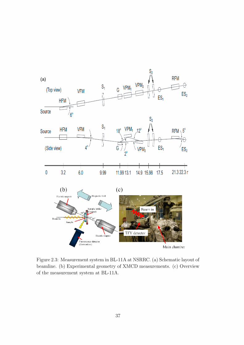
(a)
Figure 2.3: Measurement system in BL-11A at NSRRC. (a) Schematic layout of
beamline. (b) Experimental geometry of XMCD measurements. (c) Overview
of the measurement system at BL-11A.
37

Figure 2.4: Measurement system in BL-16A at PF-KEK. (a) Schematic lay-
out of beamline. (b) Experimental geometry of XMCD measurements. (c)
Overview of the measurement system at BL-16A.
preparation chamber for sample surface cleaning was connected to the mea-
surement chamber to enable transfer without breaking the ultra-high vacuum.
38
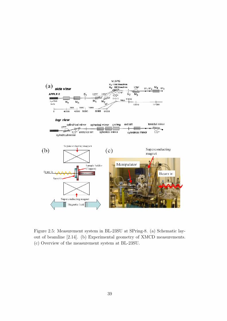
Figure 2.5: Measurement system in BL-23SU at SPring-8. (a) Schematic lay-
out of beamline [2.14]. (b) Experimental geometry of XMCD measurements.
(c) Overview of the measurement system at BL-23SU.
39

Chapter 3
X-ray magnetic circular
dichroism study of
ferromagnetic Ti1−𝑥Co𝑥O2−𝛿
thin films
3.1 Introduction
Semiconductors partially substituted with magnetic ions are called diluted
magnetic semiconductors (DMSs) are expected to be useful in spintronics
devices, where electron spins can be controlled by electric field and/or by
photons. Ferromagnetic DMS’s with Curie temperatures (𝑇C’s) higher than
room temperature are highly desirable for the development of spintronic de-
vices. To date, much work in this area has been done, mainly on II-VI
and III-V compounds doped with magnetic ions such as (Cd,Mn)Te [165]
and (Ga,Mn)As [166, 167], but their 𝑇C’s are far below room temperature.
Recently, room temperature ferromagnetism in Co-doped titanium dioxide
(TiO2) [168–171] has attracted much attention. Room-temperature ferromag-
netism was also reported in such materials as (Zn,Cr)Te [172], (Ga,Mn)N [173]
and (Al,Cr)N [174]. The near edge x-ray absorption fine structure study of
Co-doped TiO2 by Griffin et al. [175] claims that ferromagnetism is due to
𝑑-𝑑 double exchange mediated by tunneling of 𝑑 electrons within the impurity
band. Some studies that also claim the ferromagnetism of Co-doped TiO2 is
due to Co metal clusters [176–179]. The recent theoretical study by Calderon
et al. [180], electric field-induced anomalous Hall effect (AHE) study by Ya-
mada et al. [181] and x-ray photoemission spectroscopy study by Ohtsuki et
al. [182] suggested the ferromagnetism of Co-doped TiO2 is due to carrier me-
diated. However, direct information about the magnetization as a function
40

of carrier density has been lacking. Soft x-ray magnetic circular dichroism
(XMCD) at the Co 2𝑝 → 3𝑑 absorption (Co 𝐿2,3) edge is a powerful technique
to clarify this issue because it is an element-specific magnetic probe [179]. Our
previous XMCD study on rutile Co-doped TiO2 has revealed that the ferro-
magnetism is not due to segregated Co metal clusters but is due to Co2+ ions
in the TiO2 matrix [170]. However, the XMCD signal intensities were an order
of magnitude lower than that expected from the bulk magnetization [170].
In a more recent work [171], we performed x-ray absorption spectroscopy
(XAS) and XMCD studies on rutile Co-doped TiO2 not only by the surface-
sensitive total electron yield (TEY) mode but also the bulk-sensitive total
fluorescence yield (TFY) mode and found that Co ions in the bulk indeed have
a large magnetic moment of 0.8-2.2 𝜇𝐵/Co. In this work we have extended
the same approach to anatase Co-doped TiO2 and studied correlation between
magnetism and transport properties. Magnetization measurements of anatase
Ti1−𝑥Co𝑥O2−𝛿 thin films reveal ferromagnetic hysteresis behavior in the M-H
loop at room temperature with a saturation magnetization. In the bulk region
probed by the TFY mode, strong XMCD spectra with similar spectral line
shapes were obtained for all the samples. The magnetization and the XMCD
intensity increased with carrier density, consistent with the carrier-induced
origin of the ferromagnetism.
3.2 Experimental
Rutile Ti1−𝑥Co𝑥O2−𝛿 (101) epitaxial thin films with 𝑥 = 0.03, 0.05 and 0.10
were synthesized by the pulsed laser deposition method on r-Al2O3 (101) sub-
strates at 673K at different oxygen pressures, 𝑃O2= 10−6 or 10−7 Torr [183].
The samples fabricated in oxygen pressure 𝑃O2=10−6 and 10−7 Torr are named
as low-𝛿 and high-𝛿, respectively, since the number of oxygen vacancies in-
creases with decreasing oxygen pressure. The Fermi wavelength for high-𝛿 and
low-𝛿 is in the range of 1.06 nm and 3.46 nm. The carrier densities 𝑛𝑒 for high-𝛿
and low-𝛿 were in the range of 7 × 10²¹ to 2 × 1020 cm−3. Segregation of sec-
ondary phases were not observed under careful inspection by x-ray diffraction
(XRD), AFM, scanning electron microscopy (SEM), and transmission electron
microscopy (TEM). Its ferromagnetism at room temperature was confirmed by
Hall-effect measurements, magnetization measurements, and magnetic circular
dichroism (MCD) measurements in the visible region [169,183,184].
Anatase Ti1−𝑥Co𝑥O2−𝛿 (001) epitaxial thin films with 𝑥 = 0.05 were
synthesized by the pulsed laser deposition method on LaAlO3 (001) substrates
at 523 K and oxygen pressures (𝑃O2) of 5 × 10⁻⁷, 1 × 10⁻⁶ and 2 × 10⁻⁶
Torr. The resistivity increases in this order and these samples are hereafter
41

referred to metallic, intermediate, insulating samples, respectively. The carrier
densities 𝑛𝑒 were 4.1 × 10¹⁹, 1.1 × 10¹⁹ and 4.0 × 1018 cm−3, respectively and
the Fermi wavelength is 5.92 nm, 9.13 nm and 12.78 nm, respectialy. Reflection
high-energy electron diffraction was monitored during the in-situ growth. An
intensity oscillation was observed at the initial stage of the growth. The surface
morphology of the resulting films of∼40 nm thickness observed by ex-situ AFM
showed atomically flat surfaces consisting of steps and terraces. Segregation
of secondary phases were not observed under careful inspections by XRD and
TEM [181]. Ferromagnetism at room temperature was confirmed by Hall-effect
measurements and magnetization measurements.
XAS and XMCD measurements were performed at the BL-11A beamline
of the National Synchrotron Radiation Research Center, Taiwan. In XMCD
measurements, magnetic fields (H) were applied parallel to the direction of
anatase (001) and for rutile it was applied to the sample along out-of-plane.
The monochromator resolution was E/ΔE>10000, the circular polarization of
x-rays was 55%. The base pressure of the chamber was about 10−9 Torr and
the sample temperature was maintained at 300 K. The samples were placed in
an ultra-high-vacuum (UHV) experimental chamber. XAS and XMCD spectra
were obtained in the TEY and TFY modes without surface treatment in order
to avoid possible destruction of the sample surfaces. The probing depths of
the TEY mode and TFY mode were ∼5 and 100 nm, respectively.
3.3 Results and Discussion
3.3.1 Results on rutile Co-doped TiO2
Figure 3.1(a)-(b) shows magnetic properties of Ti1−𝑥Co𝑥O2−𝛿 at 300 K with
different x and electron carrier density (𝑛𝑒). It is clear from Fig 3.1 that the
magnetization M(H) was in the range 1.0-1.5 𝜇𝐵/Co with coercive force around
several tens of Oersted, and increases with 𝛿 or 𝑛𝑒. In M(H) measurements,
magnetic field was applied to the sample along out-of-plane i.e. direction of
rutile (101). AHE measurements for Ti1−𝑥Co𝑥O2−𝛿 with different 𝑛𝑒 and x also
showed the same magnetic field dependences. The resultant magnetic “phase
diagram” shows that higher 𝑛𝑒 and x induce the ferromagnetic phase as shown
in Fig 3.1(b).
In Figure 3.2, we show the Co 𝐿2,3-edge XAS and XMCD spectra of
Ti1−𝑥Co𝑥O2−𝛿 (x=0.03, 0.05 and 0.10 with low- and high-𝛿) thin films taken in
the TEY mode. In the figure, 𝜇+ and 𝜇− stand for the absorption coefficients
for photon helicity parallel and antiparallel to the Co majority spin direction,
respectively. The XMCD spectra (Δ𝜇= 𝜇+ - 𝜇−) have been corrected for the
42
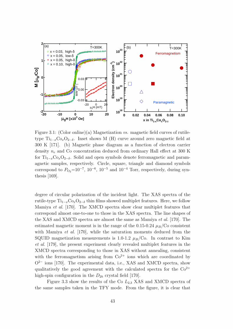
-2
-1
0
1
2
M [m
B/C
o]
-20 -10 0 10 20m0H [x103 Oe]
x = 0.03, high-δx = 0.05, low-δx = 0.05, high-δx = 0.10, high-δ
(a) T=300K
1018
1019
1020
1021
1022
1023
Ele
ctro
n d
ensi
ty (
cm-3
)0.100.080.060.040.020
x in Ti1-xCoxO2-d
Ferromagnetism
Paramagnetic
(b) T=300K
-0.03
0.00
0.03
-20 0 20
M/M
' [2T
]
µ0H (mT)
Figure 3.1: (Color online)(a) Magnetization vs. magnetic field curves of rutile-
type Ti1−𝑥Co𝑥O2−𝛿. Inset shows M (H) curve around zero magnetic field at
300 K [171]. (b) Magnetic phase diagram as a function of electron carrier
density 𝑛𝑒 and Co concentration deduced from ordinary Hall effect at 300 K
for Ti1−𝑥Co𝑥O2−𝛿. Solid and open symbols denote ferromagnetic and param-
agnetic samples, respectively. Circle, square, triangle and diamond symbols
correspond to 𝑃O2=10−7, 10−6, 10−5 and 10−4 Torr, respectively, during syn-
thesis [169].
degree of circular polarization of the incident light. The XAS spectra of the
rutile-type Ti1−𝑥Co𝑥O2−𝛿 thin films showed multiplet features. Here, we follow
Mamiya et al. [170]. The XMCD spectra show clear multiplet features that
correspond almost one-to-one to those in the XAS spectra. The line shapes of
the XAS and XMCD spectra are almost the same as Mamiya et al. [170]. The
estimated magnetic moment is in the range of the 0.15-0.24 𝜇𝐵/Co consistent
with Mamiya et al. [170], while the saturation moments deduced from the
SQUID magnetization measurements is 1.0-1.2 𝜇𝐵/Co. In contrast to Kim
et al. [179], the present experiment clearly revealed multiplet features in the
XMCD spectra corresponding to those in XAS without annealing, consistent
with the ferromagnetism arising from Co2+ ions which are coordinated by
O2− ions [170]. The experimental data, i.e., XAS and XMCD spectra, show
qualitatively the good agreement with the calculated spectra for the Co2+
high-spin configuration in the 𝐷2ℎ crystal field [170].
Figure 3.3 show the results of the Co 𝐿2,3 XAS and XMCD spectra of
the same samples taken in the TFY mode. From the figure, it is clear that
43

400
300
200
100
0
800790780Photon Energy (eV)
µ+
µ−
x = 0.03, high-δ
x = 0.05, high-δ
x = 0.05, low-δ
x = 0.10, high-δ
(a) Ti1-xCoxO2-δ, Co L2,3 XAS TEY, 300K
Inte
nsi
ty (
arb
. un
its)
100
80
60
40
20
0
x = 0.05, high-δ TEY, 300K
(b) XAS
Inte
nsi
ty (
arb
. un
its)
µ+
µ−
-4
-3
-2
-1
0
784782780778Photon Energy (eV)
(c) XMCD
Figure 3.2: (Color online) (a) Co 𝐿2,3 XAS and (b)-(c) XAS and XMCD
spectra of rutile-type Ti1−𝑥Co𝑥O2−𝛿 samples for x=0.05, high-𝛿 taken in the
TEY mode at T = 300 K and H = 1 T.
the XMCD intensities are much higher than those taken in the TEY mode.
The large difference between the bulk-sensitive TFY and surface-sensitive TEY
modes indicates that there is a magnetically dead layer of ∼ 5 nm, at the sur-
faces of the samples, which is consistent with recent measurements of the film
thickness dependence of AHE [185]. The spectral line shapes of the XAS and
XMCD spectra of the x = 0.05, high-𝛿 sample shows a clear multiplet feature
while the other samples show relatively weak multiplet features. A possi-
ble origin of the weakness of the multiplet features of other samples might
be the limited S/N ratio. The fine structure, which is indicative of Co2+,
is more pronounced in the TEY than in the TFY modes. This is because
in this compound, there should be at least as many oxygen vacancies as Co
and electrostatic interaction from the oxygen vacancies may affect Co position
significantly [186] and hence we incorporated the random crystal field in our
calculations. In the surface region, which is observed by the TEY mode, the
44

400
300
200
100
0
800790780Photon Energy (eV)
x = 0.03, high-d
x = 0.05, low-d
x = 0.05, high-d
x = 0.10, high-d
µ+
µ−
(a) Ti1-xCoxO2-d, Co L2,3 XAS
TFY, 300K X
AS
Inte
nsi
ty (
arb
. un
its)
70
60
50
40
30
20
x = 0.05 , high-d
TFY, 300K (b) XAS
In
ten
sity
(ar
b. u
nit
s)
µ+
µ−
-10
-5
0
784782780778776Photon Energy (eV)
(c) XMCD
Figure 3.3: (Color online) (a) Co 𝐿2,3 XAS and (b)-(c) XAS and XMCD
spectra of rutile-type Ti1−𝑥Co𝑥O2−𝛿 samples for x=0.05, high-𝛿 taken in the
the TFY mode at T = 300 K and H = 1 T. (d),(e) Comparison of XAS and
XMCD spectra shown in (b) and (c) with cluster-model calculation [187]
45

position of Co atoms may be optimized in a similar way because of the oxida-
tion and less structural constraint at the surface, resulting in relatively uniform
crystal field. On the other hand, in the bulk, probed by the TFY mode, the
position of Co atoms might be frozen in various local structures. The random
crystal fields in the 3D crystal lattice make the TFY spectra broad and differ-
ent from the TEY spectra. The XAS and XMCD spectra taken in the TFY
mode also show good agreement with the calculated spectra for the Co2+ in
bulk Ti1−𝑥Co𝑥O2 with random crystal fields [187].The parameters used in the
calculations listed in Table 3.1.
3.0
2.5
2.0
1.5
1.0
0.5
0
Cluster model
SQUID
TFY
x = 0.03, high-δ
TEY
(a)
Mag
net
izat
ion
(µ B
/ C
o)
T=300K
Cluster model
SQUID
TFY
x = 0.05, low-δ
TEY
(b)T=300K
3.0
2.5
2.0
1.5
1.0
0.5
01.00.80.60.40.20
Cluster model
TFY
SQUID
x = 0.05, high-δ
TEY
(c)
Magnetic field (T)
T=300K
1.00.80.60.40.20
Cluster model
x = 0.10, high-δ
SQUID
TFY
TEY
(d)
T=300K
Figure 3.4: (Color online) M-H relation of SQUID magnetization and magne-
tization estimated from the XMCD spectra Ti1−𝑥Co𝑥O2−𝛿.
Figure 3.4 shows the magnetization estimated from the XMCD spectra
46

Table 3.1: Electronic structure parameters for rutile Co-doped TiO2 thin film
used in the cluster-model calculations in units of eV : the charge-transfer energy
Δ, the on-site 3𝑑-3𝑑 Coulomb energy 𝑈𝑑𝑑, and the 3𝑑-2𝑝 Coulomb energy 𝑈𝑑𝑐
on the Co ion, the hopping integral between Co 3𝑑 and O 2𝑝 𝑉E𝑔 , and the
crystal-field 10Dq.Crystal symmetry Δ 𝑈𝑑𝑑 𝑈𝑑𝑐 𝑉E𝑔 10Dq weight(%)
𝐷2ℎ low spin 4 5 7 1.1 1.1−1.2 38%
𝑂ℎ low spin 3 6 7.5 1.1 1.1−1.2 38%
𝑂ℎ high spin 2 5 7.5 1.1 0.8−0.9 24%
taken in the TFY and TEY modes using optical sum rules [188] compared it
with M-H curves from magnetization measurements as well as cluster model
calculations. For the validity of sum rule in this case we divided the obtained
spin-magnetic moment by a correction factor 0.92 [189]. The magnetic mo-
ment obtained from cluster model calculation is 1.48 𝜇𝐵/Co. Nevertheless,
the Co magnetic moment is found to be obviously much larger in the bulk
region than in the surface region. Since the TFY suffers from self-absorption
so the magnetic moment obtained by optical sum-rule is not so accurate like
TEY mode. The magnetization estimated from the XMCD spectra taken in
the bulk-sensitive TFY mode are similar to those estimated from the SQUID
measurements as well as cluster model calculations, which strongly suggest
that the Co ions in the bulk region are responsible for the ferromagnetism
while the surface layer of the film looks like magnetically dead layer, as con-
firmed by the XMCD taken in the surface-sensitive TEY mode. TiO2 has
an extraordinary chemical stability, hence we can rule out possible surface
degradation as a cause of decrease in surface magnetization. From surface
characterization techniques such as AFM and reflection high energy electron
diffraction, we have not observed any change in the surface state. Also, from
spectroscopic techniques, we have not observed a significant time dependence
of XMCD and x-ray photoemission spectroscopy. Figure 3.1(a) shows mag-
netic hysteresis of Ti1−𝑥Co𝑥O2−𝛿 with different x. The coercive force is so
small that the hysteresis is difficult to resolve by XMCD setup. The magnetic
anisotropy with out-of-plane easy axis is not so strong in Ti1−𝑥Co𝑥O2−𝛿. As
reported by Fukumura et al. [169] , even the out-of-plane anisotropy depends
on Co content and carrier density. Thus, it is difficult to draw unified explana-
tion of the magnetic anisotropy at present. The experimental absorption and
optical MCD spectra of the Co-doped anatase and rutile TiO2 [190, 191] are
similar to the spectra obtained from the first principle calculations [192]. The
first principles calculations are found to be qualitatively or even semiquantita-
47
tively consistent with the experimental absorption and MCD measurements,
indicating that the band-structure of the Co-doped TiO2 is similar to that of
the host TiO2 [192]. The experimental MCD signals of Co-doped anatase and
rutile TiO2 are well identified by theoretical calculation [192] and they do come
from the energy band structure of the system, giving further support on the
intrinsic ferromagnetism in the Co-doped TiO2 system.
Fig 1.1 of chapter 1 shows the phase diagram for (Ga,Mn)As. In the
simple estimation we found “Y-axis = Co-band exchange/Fermi energy” for
all rutile samples were in the range of 1.5 to 16.7. Since we know that effective
mass (𝑚★) of rutile is 20𝑚0, where 𝑚0 is mass of electrons [193] and Co-band
exchange is a constant which is of order 0.1 eV for 𝑛-type carriers [56]. The
“X-axis = Carrier concentration/Co concentration” for these samples were in
the range of 0.4 to 6. Since the a few values are out of the range of the phase
diagram for (Ga,Mn)As so it is necessary to predict phase diagram for rutile
Co-doped TiO2 in future.
48

3.3.2 Results on anatase Co-doped TiO2
2
1
0
-1
-2
-1.0 -0.5 0.0 0.5 1.0
Metallic Intermediate Insulating
M [m
B/C
o]
m0H [ T ]
Ti0.95Co0.05O2-δ
(a) Anatase
T= 300K
-1.0 -0.5 0.0 0.5 1.0
Ti0.95Co0.05O2-δ
(b) Rutile
m0H [ T ]
Metallic
T= 300K
Figure 3.5: (Color online) M-H curves of Ti0.95Co0.05O2−𝛿 at 300 K. (a) Metal-
lic, intermediate and insulating anatase samples [195]. (b) Metallic rutile sam-
ple.
Figure 3.5(a) shows the magnetization curves of anatase Ti1−𝑥Co𝑥O2−𝛿
(𝑥 = 0.05) at 300 K for various carrier densities (𝑛𝑒). The 𝑛𝑒 for metallic,
intermediate and insulating samples were 4.1 × 10¹⁹, 1.1 × 10¹⁹ and 4.0 ×1018 cm−3, respectively. That of metallic rutile thin films which has the carrier
density of 7 × 1021 cm−3 is also shown in Fig 3.5(b). The saturation mag-
netization of the anatase sample is 0.6-2.1 𝜇𝐵/Co with a coercive force of ∼100 to 200 Oe. In the M(H) measurements, magnetic field was applied parallel
to the the direction of anatase (001). Anomalous Hall-effect (AHE) measure-
ments for anatase Ti1−𝑥Co𝑥O2−𝛿 with various 𝑛𝑒 also show similar magnetic
field dependences [181]. From Fig. 3.5, it is clear that the magnetization of the
anatase thin films is larger than the rutile thin films, which may be attributed
to the fact that anatase films in this study have a mobility ∼ 2-11 cm2V−1s−1
which is two orders of the magnitude higher than the mobility of rutile thin
films [169] and also anatase films have larger conductivity than rutile films.
The systematic behavior of conductivity and saturation magnetization (𝑀𝑠)
could be explained by the carrier-induced ferromagnetism mechanism; namely,
as more carriers are induced at lower (𝑃O2), the magnetic interaction becomes
stronger and results in ferromagnetism. According to the RKKY model [34],
which explains the exchange interaction between the magnetic impurity atoms
in DMS as mediated by free charge carriers, the increase in charge carrier
density can enhance the magnetic ordering.
49

300
250
200
150
100
50
0
795790785780775
XA
S In
ten
sity
(ar
b. u
nit
s)
Insulating
Intermediate
Metallic
(a)
µ+ µ-
Photon energy (eV)
Ti0.95Co0.05O2-δ
XAS in TEY mode 120
100
80
60
40
20
0 XA
S In
ten
sity
(ar
b. u
nit
s)
Metallic
(b) XAS in TEY mode
5
0
-5
784782780778Photon energy(eV)
XM
CD
Inte
nsi
ty (
arb
. un
its)
(c) XMCD in TEY mode
Metallic
300
250
200
150
100
50
0795790785780775
Co2+
high spin D2h
Calc.
Co2+
high spin Oh
Calc.
Metallic Expt.
(d)
Photon energy (eV)
XA
S In
ten
sity
(ar
b. u
nit
s)
-20
-10
0
795790785780775
Co2+
high spin D2h
Calc.
Co2+
high spin Oh
Calc.
MetallicExpt.
(e)
Photon energy (eV)
XM
CD
Inte
nsi
ty (
arb
. un
its)
Figure 3.6: (Color online) Co 𝐿2,3-edge of anatase Ti0.95Co0.05O2−𝛿 taken in the
TEY mode at T = 300 K and H = 1 T. (a) XAS. (b),(c) XAS and XMCD spec-
tra of the metallic anatase Ti0.95Co0.05O2−𝛿 sample. (d),(e) Comparison of the
XAS and XMCD spectra shown in (b) and (c) with cluster-model calculation.
50

Table 3.2: Electronic structure parameters for the anatase Co-doped TiO2
thin film used in the cluster-model calculations in units of eV to analyze the
spectra taken in the TEY mode. Δ: Charge-transfer energy, 𝑈𝑑𝑑: On-site 3𝑑-3𝑑
Coulomb energy, 𝑈𝑑𝑐: 3𝑑-2𝑝 Coulomb energy, 𝑉E𝑔 : Hopping integral between
the Co 3𝑑 and O 2𝑝 orbitals of 𝐸𝑔 symmetry, 10Dq: Crystal-field splitting.
Crystal-field symmetry Spin Δ 𝑈𝑑𝑑 𝑈𝑑𝑐 𝑉E𝑔 10Dq
𝐷2ℎ High 4 5 7 1.1 0.9
𝑂ℎ High 2 5 7.5 1.1 0.8
In Fig. 3.6(a), we show the Co 𝐿2,3-edge XAS (metallic, intermediate and
insulating thin films) and Fig. 3.6(b)-(c) XAS and XMCD spectra of (metallic
thin film) anatase Ti1−𝑥Co𝑥O2−𝛿 obtained in the TEY mode. In the figure,
𝜇+ and 𝜇− refer to the absorption coefficients for photon helicity parallel and
antiparallel to the Co majority spin direction, respectively. The XMCD spectra
Δ𝜇 = 𝜇+ - 𝜇− have been corrected for the degree of circular polarization. The
XAS and XMCD spectra of the metallic anatase Ti1−𝑥Co𝑥O2−𝛿 sample showed
multiplet features as shown by Fig 3.6(a)-(c) and agree with our cluster model
calculations using the parameter values listed in Table 3.2, as shown in Fig.
3.6(d)and (e). The multiplet features of the XMCD spectra show almost one-
to-one correspondence to those in the XAS spectra. The XAS and XMCD
spectra taken in the TEY mode for the intermediate samples also show clear
multiplet features. The spectral line shapes of the XAS and XMCD spectra for
the metallic and intermediate anatase Ti1−𝑥Co𝑥O2−𝛿 samples are also similar
to those of rutile Co-doped TiO2 results which were reported in our previous
work [170, 171]. For the insulating sample, we observed an XAS spectrum
similar to those of the metallic and intermediate samples. The estimated
magnetic moments for all samples obtained from XMCD in the TEY mode
were < 0.3 𝜇𝐵/Co. These values are larger than the 0.1 𝜇𝐵/Co which is
reported by Mamiya et al. [170]. But they are still smaller than the saturation
magnetic moments 0.6-2.1 𝜇𝐵/Co deduced from magnetization measurements.
Figures 3.7(a),(b) and (c) shows the Co 𝐿2,3 XAS and XMCD spectra of
the same samples taken in the TFY mode. From the figure, it is clear that the
XMCD intensities are much higher than those taken in the TEY mode. The
large difference between the bulk-sensitive TFY mode with ∼ 100 nm probing
depth and the surface-sensitive TEY mode with ∼5 nm probing depth suggests
that there is a magnetically dead layer of ∼ 5 nm thickness or more at the sur-
face of the samples as in the case of rutile [170,171]. The presence of a surface
dead layer of ∼ 5 nm thickness is consistent with the recent measurements
of the film-thickness dependence of AHE [195]. The spectral line shapes of
51

120
80
40
0
Metallic
XA
S In
ten
sity
(ar
b. u
nit
s) (b) XAS in TFY mode
-20
-10
0
10
784782780778 XM
CD
Inte
nsi
ty (
arb
. un
its)
Photon energy(eV)
(c) XMCD in TFY mode
Metallic
350
300
250
200
150
100
50
0
795790785780775
Metallic
Intermediate
Insulating
XA
S In
ten
sity
(ar
b. u
nit
s)
(a) XAS in TFY mode
µ+, µ-
Photon energy (eV)
Ti0.95Co0.05O2-δ
300
200
100
0
800795790785780775
Co2+
high spin D2h
Calc.
Co2+
high spin Oh
Calc.
35% D2h LS+ 35% Oh LS+30% Oh HS
MetallicExpt.
(d)
Photon energy (eV)
XA
S In
ten
sity
(ar
b. u
nit
s)
Calc.
-50
-40
-30
-20
-10
0
10
20
800795790785780775
Co2+
high spin D2h
Calc.
Co2+
high spin Oh
Calc.
35% D2h LS+ 35% Oh LS+ 30% Oh HS Calc.
Photon energy (eV)
(e)
MetallicExpt.
XM
CD
Inte
nsi
ty (
arb
. un
its)
Figure 3.7: (Color online) Co 𝐿2,3-edge of anatase Ti0.95Co0.05O2−𝛿 taken in
the TFY mode at T = 300 K and H = 1 T. (a) XAS. (b),(c) XAS and
XMCD spectra of anatase Ti0.95Co0.05O2−𝛿 for metallic sample in the TFY
mode. (d),(e) Comparison of XAS and XMCD spectra shown in (b) and (c)
with cluster-model calculation [196].
52
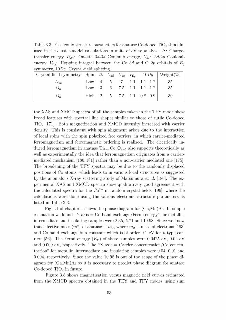
Table 3.3: Electronic structure parameters for anatase Co-doped TiO2 thin film
used in the cluster-model calculations in units of eV to analyze. Δ: Charge-
transfer energy, 𝑈𝑑𝑑: On-site 3𝑑-3𝑑 Coulomb energy, 𝑈𝑑𝑐: 3𝑑-2𝑝 Coulomb
energy, 𝑉E𝑔 : Hopping integral between the Co 3𝑑 and O 2𝑝 orbitals of 𝐸𝑔
symmetry, 10Dq: Crystal-field splitting.Crystal-field symmetry Spin Δ 𝑈𝑑𝑑 𝑈𝑑𝑐 𝑉E𝑔 10Dq Weight(%)
𝐷2ℎ Low 4 5 7 1.1 1.1−1.2 35
𝑂ℎ Low 3 6 7.5 1.1 1.1−1.2 35
𝑂ℎ High 2 5 7.5 1.1 0.8−0.9 30
the XAS and XMCD spectra of all the samples taken in the TFY mode show
broad features with spectral line shapes similar to those of rutile Co-doped
TiO2 [171]. Both magnetization and XMCD intensity increased with carrier
density. This is consistent with spin alignment arises due to the interaction
of local spins with the spin polarized free carriers, in which carrier-mediated
ferromagnetism and ferromagnetic ordering is realized. The electrically in-
duced ferromagnetism in anatase Ti1−𝑥Co𝑥O2−𝛿 also supports theoretically as
well as experimentally the idea that ferromagnetism originates from a carrier-
mediated mechanism [180, 181] rather than a non-carrier mediated one [175].
The broadening of the TFY spectra may be due to the randomly displaced
positions of Co atoms, which leads to in various local structures as suggested
by the anomalous X-ray scattering study of Matsumura et al. [186]. The ex-
perimental XAS and XMCD spectra show qualitatively good agreement with
the calculated spectra for the Co2+ in random crystal fields [196], where the
calculations were done using the various electronic structure parameters as
listed in Table 3.3.
Fig 1.1 of chapter 1 shows the phase diagram for (Ga,Mn)As. In simple
estimation we found “Y-axis = Co-band exchange/Fermi energy” for metallic,
intermediate and insulating samples were 2.35, 5.71 and 10.98. Since we know
that effective mass (𝑚★) of anatase is 𝑚0, where 𝑚0 is mass of electrons [193]
and Co-band exchange is a constant which is of order 0.1 eV for 𝑛-type car-
riers [56]. The Fermi energy (𝐸𝐹 ) of these samples were 0.0425 eV, 0.02 eV
and 0.009 eV, respectively. The “X-axis = Carrier concentration/Co concen-
tration” for metallic, intermediate and insulating samples were 0.04, 0.01 and
0.004, respectively. Since the value 10.98 is out of the range of the phase di-
agram for (Ga,Mn)As so it is necessary to predict phase diagram for anatase
Co-doped TiO2 in future.
Figure 3.8 shows magnetization versus magnetic field curves estimated
from the XMCD spectra obtained in the TEY and TFY modes using sum
53

3.0
2.5
2.0
1.5
1.0
0.5
0.01.00.80.60.40.20.0
Cluster model
XM
CD
Inte
nsity
(µ
B/C
o)
(a) Metallic
SQUIDTFY
TEY
Magnetic field (T)1.00.80.60.40.20.0
Cluster model
(b) Intermediate
Magnetic field (T)
SQUIDTFY
TEY
1.00.80.60.40.20.0
Cluster model
(c) Insulating
SQUID
TFY
TEY
Magnetic field (T)
Figure 3.8: (Color online) Magnetization as a function of magnetic field ob-
tained from the XMCD intensities of anatase Ti0.95Co0.05O2−𝛿 compared with
M-H curves obtained using a SQUID.
rules [170], as compared with the M-H curves measured using a SQUID. We
have divided the obtained spin-magnetic moment by a correction factor of
0.92 given by Teramura et al. [189]. The Co magnetic moment is found to be
obviously much larger in the bulk region than in the surface region. These
results are also consistent with the x-ray photoemission spectroscopy study by
Yamashita et al. [197]. Since we know that TFY suffers from self-absorption
and therefore it will saturate the XAS signal. This saturated XAS signal will
reduce XMCD signal. Because of this very fact, we can conclude that the real
value of magnetic moment in bulk should be even higher than the measured
TFY value in metallic and intermediate samples which are reported in the
present work. Accordingly, our observation by using the TEY and TFY modes
are validated. The magnetic moment obtained from cluster-model calculation
(Table 3.3) is 1.6 𝜇𝐵/Co, which is similar to the magnetization of ∼ 2 𝜇𝐵/Co
deduced from the TFY results and the SQUID measurement as shown in Fig
3.8. These results suggest that the Co ions in the bulk region are responsible
for the ferromagnetism in anatase Ti1−𝑥Co𝑥O2−𝛿.
54

3.4 Conclusion
In conclusion, we have studied the high temperature ferromagnetism observed
in rutile-type Ti1−𝑥Co𝑥O2−𝛿 films using x-ray magnetic circular dichroism at
the Co 𝐿2,3 edges (both in the TEY and TFY mode). These results represent
that the high temperature ferromagnetism is originated from the Co2+ atoms,
most probably charge carriers induce the ferromagnetism. The magnetic mo-
ment of the Co ions as long as 0.82-2.25 𝜇𝐵/Co was first observed by the bulk
sensitive TFY method. The magnetic moment value deduced with the TEY
mode ( 0.15-0.24 𝜇𝐵/Co) indicates the presence of a magnetically dead layer
of ∼ 5 nm thickness on the sample surface.
We have also provided experimental evidence for carrier-induced ferro-
magnetism of cobalt-doped anatase TiO2 thin films using XMCD at the Co
𝐿2,3 edges in both the TEY and TFY modes. The large magnetic moment of
the Co ions, 0.6-2.4 𝜇𝐵/Co, was observed by the bulk-sensitive TFY method.
The carrier-induced origin of ferromagnetism at room-temperature in anatase
Ti1−𝑥Co𝑥O2−𝛿 is confirmed on the basis of the element-specific XMCD study
at the surface as well as in bulk. In the bulk-sensitive TFY mode, the position
of Co2+ atoms seems to be displaced from the Ti4+ sites, resulting in more
random crystal fields. Good agreement is demonstrated not only in magneti-
zation and AHE but also in the magnetic field dependences of XMCD. The
magnetic moment values deduced with the TEY mode was < 0.3 𝜇𝐵/Co, in-
dicating the presence of a magnetically dead layer of ∼5 nm thickness at the
sample surfaces.
55
Chapter 4
X-ray magnetic circular
dichroism study of
ferromagnetic BiFe1−𝑥Co𝑥O3
thin films
4.1 Introduction
Multiferroics have attracted tremendous interest in recents years, which
simultaneously show spontaneous electric and magnetic ordering in the same
phase, [198–201] because of their potential applications in the fields of infor-
mation storage, spintronics, and sensor, and also because of their underlying
fascinating fundamental physics [198]. There are not many natural multiferroic
materials exist because of the incompatibility between the conventional cation
off-center distortion mechanism in ferroelectrics and the formation of magnetic
moments [199] at the cation sites. Most of multiferroics have, however, very
different ferroelectric and magnetic ordering temperatures and the magnetic
ordering is usually antiferromagnetic. BiFeO3 (BFO) is a rare multiferroic ma-
terial which is both ferroelectric (𝑇C ∼1103 K) and antiferromagnetic (𝑇N ∼643 K) at room temperature, and exhibits weak ferromagnetism because of the
canted spin structure [202]. The magnetic structure is a nearly 𝐺-type antifer-
romagnet, i.e., the Fe magnetic moments are coupled ferromagnetically within
the pseudocubic (111) planes and coupled antiferromagnetically between ad-
jacent planes. However, the additional incommensurate spin modulation leads
to the cancellation of macroscopic magnetization. This incommensurate spiral
spin structure can be suppressed by applying high magnetic field [204], chem-
ical substitution [205] or epitaxial strain in the case of thin films [206], which
prohibits the linear magnetoelectric effect from being observed [203].
56
It has been predicted that spontaneous magnetization can be induced in
BFO by mixed valence or chemical substitution either changing the Fe-O-Fe
bond angle or a statistical octahedra distortion of the FeO6 [198,201,207]. In
the case of thin films, it has been shown that heteroepitaxially strained BFO
films are ferromagnetic at room temperature and show a remarkably large
magnetoelectric effect [208]. The structure and properties of the bulk single
crystals form have been extensively studied [209–214], and they have been
shown to possess a rhombohedrally distorted perovskite structure (a = b = c
= 5.63 A, 𝛼 = 𝛽 = 𝛾 = 59.4∘) at room temperature. Wang et al. [206] recently
reported multiferroic behavior, with ferromagnetic and ferroelectric polariza-
tions that are both large at room temperature, in thin strained films of BFO.
They reported that a 70-nm film shows both an enhanced ferroelectric polariza-
tion (90 𝜇C.cm−2) and a substantial magnetization (1 𝜇𝐵/Fe). This remains
the only report of a robust room temperature multiferroic and suggests the
potential for novel devices that exploit the anticipated strain-mediated mag-
netoelectric coupling between the two ordered ground states. Sakamoto et al.
have reported that the resistivity of BFO improves markedly with substitution
of a small amount of Mn ions for Fe. The electrical properties of Mn-doped
BFO have been attributed to its characteristic electronic structure, including
its band gap, degree of hybridization, and the valence state [215]. So far the
electronic structure and magnetic properties of Co-doped BFO (BFCO) has
not been clarified experimentally.
X-ray absorption spectroscopy (XAS) and magnetic circular dichroism
(XMCD) are effective techniques for probing the electronic and magnetic prop-
erties of complex solids. The optical process involved in XAS and XMCD is
a local one because of the localized core state and the dipole selection rules.
Several studies have utilized these techniques to examine the electronic and
magnetic states of such materials [210–213]. These studies have focused on
multiferroic BFO-based materials and investigated the electronic and magnetic
structure at the Fe 2𝑝 core absorption edge [210–213].
In this thesis, we investigated the electronic structure and the magnetic
properties of BFCO thin films grown on single-crystal LaAlO3 (LAO) (001)
substrates using XAS and XMCD. XAS and XMCD enabled us to study the
element-specific electronic properties of the BFCO thin films. Based on our
experimental results, we discuss the origin of ferromagnetism at room temper-
ature in BFCO thin films.
57

4.2 Experimental
BFCO thin films with a thickness of ∼ 260 nm were grown on LAO (001) sub-
strates using a chemical solution deposition technique. Prior to the deposition
a 100-nm-thick SrRuO3 (SRO) was grown using the pulsed laser deposition
method to serve as a base electrode. These substrates were spin-coated (for
30 s at 4000 rpm) using a solution containing Bi, Co, and Fe organometallic
compounds (Koujundo Chemical Laboratory Co. Ltd.) in a xylene carrier in
the desired ratio at a concentration of 0.2 mol/kg. The samples were then
heated in air at 250∘C for 5 min. Repeating this coating-heating sequence
13 times yielded BFCO films that were about 260 nm thick. After the films
were annealed for 60 min in a 5% ozone-oxygen mixture in a tube furnace at
420∘C, the BFCO/SRO(001)/LAO(001) samples were subjected to a second
annealing stage at 435∘C for 30 min to improve their crystallinity. Structural
characterization was carried out using x-ray diffraction (XRD), which demon-
strated a clear single phase [214]. This XRD experiments confirmed that, as
the Co content grows, BFCO moves from rhombohedral (R) to tetragonal (T)
symmetry and both phases (R and T) exists for Co content= 0.10 to 0.20.
However, it converted to T phase after Co content= 0.20. Transmission elec-
tron spectroscopy (TEM) images show that the existence of secondary phases
in the form of cluster.
The XAS and XMCD measurements were performed at the undulator
beam line BL-23SU of SPring-8, Japan. The measurements were performed
at room temperature in an applied magnetic field over the range up to ± 3T.
The propagation vector of photons with circular polarization was parallel to
the magnetic field and perpendicular to the sample surface. The spectra were
collected in the total electron yield (TEY) mode which has a probing depth of
∼5 nm. The monochromator resolution was E/ΔE>10000, and the circular
polarization of the x-rays was 95%. The base pressure of the chamber was
about 10−9 Torr. The XAS and XMCD spectra were obtained in the TEY
mode without surface treatment.
4.3 Results and Discussion
Figure 4.1 shows the Fe 2𝑝-3𝑑 XAS spectra of the BFO sample consisting
of 𝐿3 (2𝑝3/2) and 𝐿2 (2𝑝1/2) regions. This Fe 2𝑝-3𝑑 XAS spectrum of BFO is
compared with the Fe 2𝑝 XAS spectra of 𝛼-Fe2O3, Fe3O4, and FeO [216,217].
The line shape of the XAS spectrum of the BFO sample shows a two-peak
structure at the 2𝑝3/2 (𝐿3) edge is similar to 𝛼-Fe2O3, indicating that the Fe
ions in BFO were in the trivalent state (𝑂ℎ) site [212, 218]. This result is
58

250
200
150
100
50
0
-50
730725720715710705Photon energy(eV)
XA
S in
ten
sity
(ar
b. u
nit
s)
Fe 2p3/2
Fe 2p1/2
a-Fe2O3, Fe3+
BiFeO3 thin film
Fe 2p-3d XAS at 300K
Fe3O4 Mixed Fe3+
& Fe2+
FeO, Fe2+
Regan et al
Regan et al
Regan et al
Figure 4.1: (Color online) Fe 2𝑝-3𝑑 XAS spectra of the BiFeO3 thin film com-
pared with those of 𝛼-Fe2O3, FeO, Fe3O4 [216,217].
consistent with the electron spin resonance study of BFO [219]. Therefore, the
XAS spectrum of the BFO sample indicated that the valence state of Fe is 3+.
Our experimental results do not include the presence of Fe2+ ions, as has been
suggested by the previous XAS and XMCD studies of BFO thin films [211].
Figures 4.2(a) and (b) show the Fe 2𝑝-3𝑑 XAS spectra of BFO and
BFCO samples with opposite magnetization directions recorded using circular
polarized x-rays. Their difference spectra, i.e., XMCD spectra, are shown in
Figs. 4.2(c). Here, the XAS spectra obtained in applied magnetic fields of
+3.0 and -3.0 T are denoted by 𝜇+ and 𝜇−, respectively. Three sharp peaks
occurred in the XMCD spectra around ℎ𝜈 = 708.5, 709.7, and 710.5 eV. Figure
4.2(d) shows that the Fe 2𝑝-3𝑑 XMCD spectrum of BFCO films were different
from those of the FeO [220], indicating that the magnetism in these samples
did not arise from Fe metal segregation. Also XMCD spectra of BFCO films
are compared with those of GaFeO3 (GFO), where the Fe3+ ions are located
at the 𝑂ℎ sites [221], 𝛾-Fe2O3 nanoparticles, where the Fe3+ ions are located
at both octahedral (𝑂ℎ) and the tetrahedral (𝑇𝑑) sites [222] and Fe3O4, where
Fe3+ ions are located at both the 𝑇𝑑 and 𝑂ℎ sites and Fe2+ ions are located at
59

140
120
100
80
60
40
20
0
XA
S in
tens
ity (
arb.
uni
ts) BiFeO3 thin film
Fe 2p-3d XAS at 300K
s+
s-H= ±3.0 T
(a)
350
300
250
200
150
100
50
0730725720715710705
XA
S In
tens
ity (
arb.
uni
ts)
Co=30%
Co=20%
Co=15%
Co=05%
Co=0%
Fe 2p-3d XAS at 300K, H= ±3T
BiFe1-xCoxO3 (x = 0 to 30%)
σ+
σ−
(b)
Photon Energy(eV)
-20
-10
0
10
Co=30% Co=20% Co=15% Co=5.0% Co=0.0%
XM
CD
Inte
nsity
(ar
b. u
nits
)
Fe 2p-3d XMCDBiFe1-xCoxO3 (x = 0 to 30%)
(c)
150
100
50
0
-50
-100
730725720715710705
A
B
C
Fe 2p-3d XMCD at 300K
GaFeO3 J.-Y. Kim et al.,
γ−Fe2O3 nano-particles
S.B. Profeta et al.,
BiFe1-xCoxO3
Fe3O4 J.Chen et al.,
XM
CD
Inte
nsity
(ar
b. u
nits
)
Photon Energy(eV)
Fe3+
(Oh)
Fe3+
(Oh), Fe2+
(Oh)
Fe3+
(Td)
Fe3+
(Oh)Fe
3+(Oh)
Fe3+
(Td)
Fe3+
(Oh)Fe
3+(Oh)
(d)
Figure 4.2: (Color online) Fe 2𝑝-3𝑑 XAS and XMCD spectra of the
BiFe1−𝑥Co𝑥O3 thin films. (a) XAS spectra in magnetic fields of ± 3T at
300 K. (b) XAS spectra of the BiFe1−𝑥Co𝑥O3 (𝑥 = 0 to 0.30) thin films in
magnetic fields of ± 3T at 300 K. (c) XMCD spectra of the BiFe1−𝑥Co𝑥O3
(𝑥 = 0 to 0.30) thin film in magnetic fields of ± 3T at 300 K. (d) Compari-
son of the experimental XMCD spectra of BFCO with the XMCD spectra of
GaFeO3 [221], 𝛾-Fe2O3 [217], Fe3O4 [222] and FeO [220].60
the 𝑂ℎ sites [217]. The XMCD spectrum of Fe3O4, which displays overlapping
contributions of the Fe3+ and Fe2+ ion, and that of GFO with Fe3+ ions at the
𝑂ℎ sites are different from the spectra of BFCO thin films. On the other hand,
the spectral line shape of the 𝛾-Fe2O3 thin films, where the XMCD signals arose
from the antiferromagnetically coupled Fe3+ (𝑂ℎ) ions and Fe3+(𝑇𝑑), was nearly
identical to that of the BFCO thin films. This indicates that the magnetism
in the BFCO thin films is mainly originated from antiferromagnetially coupled
Fe3+ ions located at both the 𝑂ℎ and 𝑇𝑑 sites. Since in BFCO, Fe ions do not
occupy 𝑇𝑑 sites, this result suggests that the observed ferromagnetism and/or
superparamagnetic behavior in the BFCO thin films is mainly arose from 𝛾-
Fe2O3 like species as a secondary phase, as has been discussed as the origin of
the magnetic moment in BFCO thin films [223].
Figure 4.3(a) shows the Fe 2𝑝-3𝑑 XMCD spectrum of BiFe0.80Co0.20O3
thin films measured in various applied magnetic fields. It can be seen that
the XMCD peak intensity remains high down to an applied field of 0.1 T
[Figs. 4.3(a) and (b)], indicating that the ferromagnetism exists in this sam-
ple. In Fig. 4.3(a), peaks from the Fe3+ ions located at the 𝑇𝑑 and 𝑂ℎ sites
had different signs. This clearly implies the presence of Fe3+ (𝑇𝑑)- Fe3+ (𝑂ℎ)
antiferromagnetic coupling. This XMCD line shape is independent of the mag-
netic field, indicating that the ferromagnetism originates from the antiferro-
magnetic coupled Fe3+ ions at the 𝑂ℎ and 𝑇𝑑 sites. The Fe3+ ions occupy
two sets of nonequivalent positions are (𝑇𝑑 and 𝑂ℎ sites) in unequal numbers
and are oriented in the antiparallel directions, so that there is a net magnetic
moment [218], i.e., the ferromagnetism is caused by the difference in the num-
ber of Fe atoms between the up and down spins on the 𝑇𝑑 (𝑂ℎ) and 𝑂ℎ (𝑇𝑑)
sites respectively. Indeed, room-temperature ferromagnetism in 𝛾-Fe2O3 arises
from such Fe3+-Fe3+ antiferromagnetic coupling [224]. The magnitude of the
magnetic moment was quantitatively estimated using the XMCD spin sum
rule [220] to be ∼ 0.03 𝜇𝐵/Fe for BFO, consistent with our SQUID measure-
ment. This magnetic moment is also consistent with the canted moment in
bulk BFO (0.03 𝜇𝐵/Fe) [225]. Therefore, the magnetic moment of Fe in BFCO
samples may arises from 𝛾-Fe2O3 as a secondary phase, although we could not
observe peaks from 𝛾-Fe2O3 in the XRD spectra. This may be because of
the nanosized dimensions of 𝛾-Fe2O3 [223]. It is to note that existence of the
secondary phases were been confirmed by TEM by our collaborator.
The magnetic moment of Fe in the BiFe0.80Co0.20O3 thin film obtained
from the sum rule and the magnetization data are shown in Figs. 4.4(b).
Since the value of saturation magnetization was ∼1.25𝜇𝐵/Fe for 𝛾-Fe2O3, the
proportion of the 𝛾-Fe2O3 phase in the BiFe0.80Co0.20O3 sample was was es-
timated to be more than ∼11%. The M-H curve obtained from the XMCD
61

-30
-20
-10
0
10
20
30
730725720715710705
B
AC
3.0T2.0T1.0T0.5T0.1T
XM
CD
Inte
nsity
Photon Energy(eV)
(a) Fe 2p-3d XMCD
Fe3+
(Td)
Fe3+
(Oh)Fe3+
(Oh)
BiFe0.80Co0.20O3 thin film at 300K
1.4
1.2
1.0
0.8
0.6
0.4
0.2
0.03.02.52.01.51.00.50.0
Mag
netic
mom
ent (
µB
/Fe)
Magnetic field (T)
(b) BiFe0.80Co0.20O3 thin film at 300K
Fe
Figure 4.3: (Color online) Magnetic field dependence of the Fe 2𝑝-3𝑑 XMCD
spectra of the BiFe0.80Co0.20O3 thin film. (a) Spectra measured at various
magnetic fields. (b) Magnetic moment of Fe obtained from the XMCD intensity
as a function of magnetic field.
62

1.4
1.2
1.0
0.8
0.6
0.4
0.2
302520151050
(b) H= ±3T
Fe
% Co in BFO
Mag
netic
mom
ent (
µB
/ ion
)
XMCD
T=300K
0.3
0.2
0.1
0.0
Mag
neiz
atio
n (µ
B/ f
.u.)
SQUID
(a) H=±1
T=300K
Figure 4.4: (Color online) (a) Magnetization of BiFe1−𝑥Co𝑥O3 (𝑥 = 0 to 0.30)
thin films as a function of Co content in BiFeO3 obtained from SQUID. (b)
Magnetization of Fe in BiFe1−𝑥Co𝑥O3 (𝑥 = 0 to 0.30) thin films as a function
of percent of Co content in the BFCO thin films obtained from XMCD.
63
measurements was larger than those from the SQUID measurements. A pos-
sible reason for this discrepancy is that the surfaces of the films had a higher
magnetization than the bulk. Since TEY mode is surface sensitive and probing
depth of ∼5 nm however, SQUID is bulk sensitive. The shape of Fe magnetic
moments with Co content obtained from XMCD as well as SQUID are same
which is clear from Fig.4.4. From the shape of M-H curve we calculated the
Curie constant of Fe from the paramagnetic part of the XMCD intensity, and
found the Curie constant to be ∼ 591 J.K/mol T2, which is much larger than
the Curie constant of Fe3+(S = 5/2) ∼ 32 J.K/mol T2. This means that there
is strong ferromagnetic interaction between the Fe ions. Hence, we may also
consider that BFCO/𝛾-Fe2O3 forms a nanocomposite and can show a strong
magnetoelectric coupling response, because BFCO is strongly ferroelectric and
𝛾-Fe2O3 is strongly ferromagnetic.
Figure 4.5(a) shows the Co 2𝑝 XAS spectrum of BFCO. Because the Co
concentration was low, the intensities were low. The XMCD data are shown
in Fig. 4.5(b). The spectrum is derived from the 𝐿3 (2𝑝3/2) edge occuring at
∼ 642 eV and the 𝐿2 (2𝑝1/2) edge occurring at ∼ 653 eV. It can be clearly
seen that the Co 2𝑝 XAS spectrum of BFCO thin films was similar to that of
LaCoO3 (with Co3+) at high temperatures (650 K) but different from that of
CoO [226] (with Co2+), whose spectra are shown in Fig. 4.5(c). Thus the result
indicates that the Co ions are mainly in the trivalent high-spin states [227].
In addition, the spectra of other Co content are identical, indicating that the
valence state of the Co ions did not change with Co content. Similarly, the
XMCD peak intensity was also nearly independent of Co content. It can be
seen that the XMCD peak intensity approached zero as the magnetic field
goes to zero, as shown in Fig. 4.5(d), indicating that the Co ions were in the
paramagnetic. We calculated the Curie constant of Co from the data shown
Fig. 4.5(d) and found the value of the Curie constant was ∼ 67 J.K/mol T2
at 300 K which is smaller than the Curie constant of Co3+ (S = 2) of ∼ 100
J.K/mol T2. This means that most of the Co ions have an antiferromagnetic
interaction, and the participation of Co ions in the magnetism of BFCO thin
films is low.
The magnetic moment of the Fe and Co ions estimated using the XMCD
spin sum rule [219] are shown in Fig. 4.6(a). The Co magnetic moment was
nearly independent of Co content unlike Fe, and the peak at 20% Co content
showed only a minor influence.
Now we discuss the mechanism of ferromagnetism in the BFCO thin
films. The presence of magnetism in the BFCO thin film, at room temperature
is explained by the existence of nearest-neighbour Fe-Co pairs which cause
the ferromagnetic alignment of the Fe and Co 𝑑-moments under 180∘ super-
64
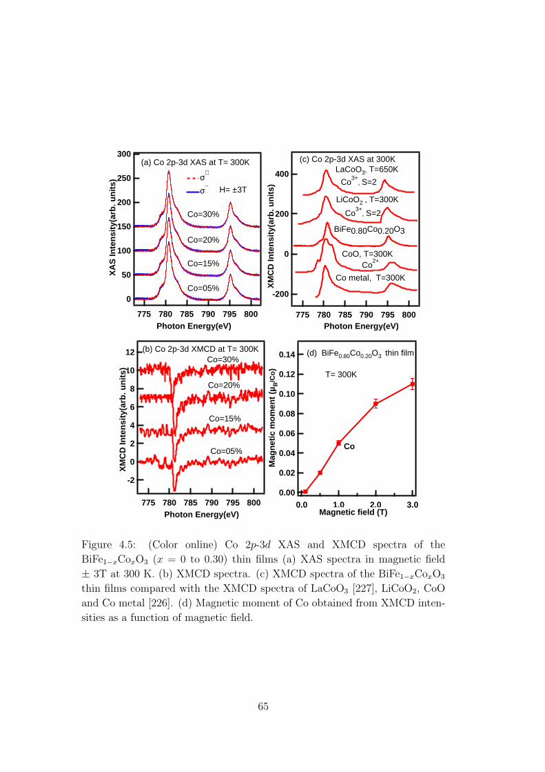
300
250
200
150
100
50
0
800795790785780775
XA
S In
tens
ity(a
rb. u
nits
)
Co=05%
Co=15%
Co=20%
Co=30%
(a) Co 2p-3d XAS at T= 300K
H= ±3T
σ+
σ−
Photon Energy(eV)
12
10
8
6
4
2
0
-2
800795790785780775
Co=05%
Co=15%
Co=20%
Co=30%
XM
CD
Inte
nsity
(arb
. uni
ts)
Photon Energy(eV)
(b) Co 2p-3d XMCD at T= 300K
400
200
0
-200
800795790785780775
LaCoO3, T=650K
LiCoO2 , T=300K
CoO, T=300K
Co metal, T=300K
BiFe0.80Co0.20O3
(c) Co 2p-3d XAS at 300K
Photon Energy(eV)
Co3+
, S=2
Co3+
, S=2
Co2+
XM
CD
Inte
nsity
(arb
. uni
ts)
0.14
0.12
0.10
0.08
0.06
0.04
0.02
0.003.02.01.00.0
Magnetic field (T)
Mag
netic
mom
ent (
µB
/Co)
(d) BiFe0.80Co0.20O3 thin film
Co
T= 300K
Figure 4.5: (Color online) Co 2𝑝-3𝑑 XAS and XMCD spectra of the
BiFe1−𝑥Co𝑥O3 (𝑥 = 0 to 0.30) thin films (a) XAS spectra in magnetic field
± 3T at 300 K. (b) XMCD spectra. (c) XMCD spectra of the BiFe1−𝑥Co𝑥O3
thin films compared with the XMCD spectra of LaCoO3 [227], LiCoO2, CoO
and Co metal [226]. (d) Magnetic moment of Co obtained from XMCD inten-
sities as a function of magnetic field.
65
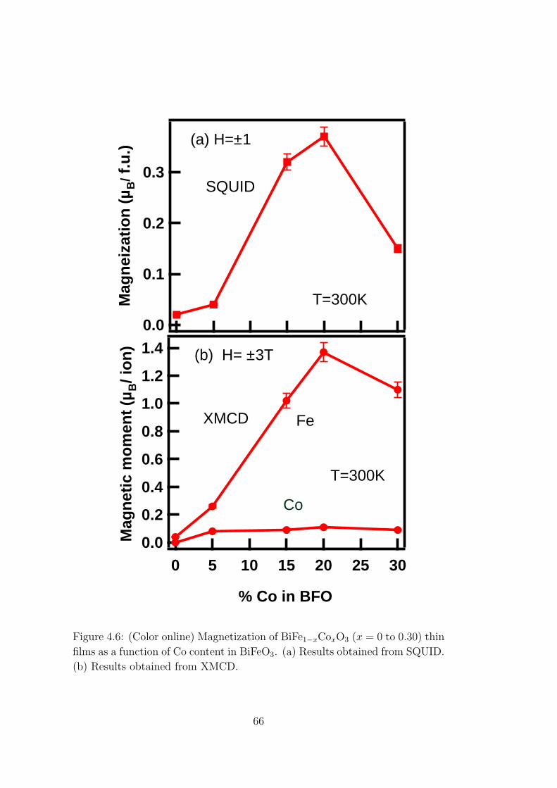
0.3
0.2
0.1
0.0
Mag
neiz
atio
n (µ
B/ f
.u.)
SQUID
(a) H=±1
T=300K
1.4
1.2
1.0
0.8
0.6
0.4
0.2
0.0302520151050
(b) H= ±3T
Fe
Co
% Co in BFO
Mag
netic
mom
ent (
µB/ i
on)
XMCD
T=300K
Figure 4.6: (Color online) Magnetization of BiFe1−𝑥Co𝑥O3 (𝑥 = 0 to 0.30) thin
films as a function of Co content in BiFeO3. (a) Results obtained from SQUID.
(b) Results obtained from XMCD.
66

exchange interaction. Since both Fe and Co ions are formally in the 3+ valance
states, BFCO is an example of a 𝑑5-𝑑6 orbital combination, and the magnetic
coupling between Fe3+ and Co3+ was predicted to be ferromagnetic in terms of
super-exchange [228–230]. If some of the Fe3+ (𝑑5)ions in the cubic structure
are replaced by Co3+ (𝑑6), the antiferromagnetic part of the nearest neighbor
coupling -now between Fe3+ (𝑑5) and Co3+ (𝑑6)−is slightly reduced and, in fact,
ferromagnetic interaction wins. This can be explained by the last electron of
𝑡2𝑔 of the Co3+, which will jump to 𝑡2𝑔 of the Fe3+ and will return back to 𝑡2𝑔of Co3+ and so it will gain ferromagnetism.
4.4 Conclusion
We have performed XAS and the XMCD measurements on BFCO thin films,
which exhibit ferromagnetism at 300 K. The XAS and XMCD line shape of
Fe ions in BFCO thin films are independent of the magnetic field, indicating
that the ferromagnetism originates from the antiferromagnetic coupled Fe3+
ions at the 𝑂ℎ and 𝑇𝑑 sites and ferromagnetism behavior in the BFCO thin
films is mainly arose from 𝛾-Fe2O3 like species as a secondary phase (i.e. fer-
romagnetism behavior in the BFCO thin films is mainly arose from extrinsic
behavior). The magnetic moment of Fe increases with Co content up to 20%
and after that it decreases. The Co ions are in the trivalent high-spin states
and are largely paramagnetic. The Co magnetic moment is nearly independent
of Co content, unlike Fe, and the peak at 20% Co has only a minor influence.
Surface Fe ions in these films also showed a significant enhancement compared
with a bulk sample probed by XMCD.
67

Chapter 5
Effect of off-stoichiometry in
Heusler alloy thin film on
spin-dependent tunneling
characteristics of
Co2Mn𝛽𝑍/MgO (𝑍= Ge, Si)
magnetic tunnel junctions
studied by x-ray magnetic
circular dichroism
5.1 Introduction
Magnetic tunnel junctions (MTJs) have recently been widely studied as mag-
netic storage devices and magnetic sensors. To improve their performance, it is
very important to understand the nature of spin-dependent conduction and de-
velop MTJs having a high tunnel magnetoresistance (TMR) ratio with highly
spin-polarized ferromagnetic electrodes. In this context, a fully epitaxial MTJ
made of an MgO tunnel barrier and half-metallic ferromagnetic electrodes is
very promising because the single-crystalline MgO enables coherent tunneling
through the Δ1 band that is conserving the highly polarized electron spins of
the half-metallic ferromagnetic electrodes. Fully epitaxial Fe/MgO/Fe MTJs,
in which Fe electrodes feature a half-metallic nature for the Δ1 band electrons,
have experimentally shown a TMR ratio of 180% (Ref. [231]) at room temper-
68

ature (RT) owing to coherent tunneling of the Δ1-band electrons. This value
is much higher than those in conventional MTJs consisting of polycrystalline
electrodes and an amorphous AlO𝑥 tunnel barrier.
Co-based full Heusler alloys Co2𝑌 𝑍 such as Co2MnGe and Co2MnSi
are also promising candidates for ferromagnetic electrodes in MTJs, because
theories have predicted that they are ideal half metals [93, 94, 232, 233]. In
fact, TMR ratios of several hundred percent in Co-based full Heusler alloys
with an MgO tunnel barrier have recently been reported [234–238]. Here,
the TMR ratio is defined as [TMR ratio]=(𝑅𝐴𝑃 -𝑅𝑃 ) /𝑅𝑃 in terms of the
resistances for the parallel (𝑅𝑃 ) and antiparallel (𝑅𝐴𝑃 ) geometries [239]. The
(anti) parallel geometry means that electrode 1 is (anti) ferromagnetically
coupled with electrode 2 across the thin nonmagnetic tunnel barrier. Assuming
ideal half metals without interface state (Jullieres model), [240] the formula
can be written as [TMR ratio]=2𝑃1𝑃2 / (1-𝑃1𝑃2), where 𝑃1 and 𝑃2 are the spin
polarizations at the Fermi level (𝐸𝐹 ) of electrodes 1 and 2, respectively [175].
In this model, if the Co-based full Heusler alloys are perfectly half metallic,
i.e., if 𝑃1 and 𝑃2 are equal to 1, the TMR ratio must be infinite. The TMR
ratio of several hundred percent in real Heusler alloy/MgO MTJs implies that
the half metallicity might have been deteriorated for some reason.
A disorder-free 𝑋2𝑌 𝑍 full Heusler alloy has the 𝐿21 crystal structure
having four fcc sublattices. When the elements 𝑌 and 𝑍 are randomly located,
the crystal structure changes to 𝐵2. When 𝑌 , 𝑍, and 𝑋 are disordered, it
changes to 𝐴2. The crystal structure change from 𝐿21 to 𝐵2 or 𝐴2 is one
of the possible reasons to reduce the spin polarizations at 𝐸𝐹 . In addition
a numerical study [241] suggests that lattice distortions and the existence of
impurities at the interfaces could also reduce the spin polarization. Hence,
high-quality interfaces are the key for obtaining high TMR ratios. Thus, it is
very important to characterize the interfacial magnetic and electronic states
of Heusler alloy/MgO MTJs.
Asakura et al. [37] studied the CMG film-thickness dependence of XMCD
and magnetic moments of seven CMG/MgO samples with various CMG thick-
nesses ranging from 1 to 172 monolayers (MLs). They reported that the XAS
and XMCD spectral shapes for thick samples (𝑡CMG ≥ 4 ML) were similar
to those for bulk CMG, [243] and neither the Mn nor Co atoms were oxi-
dized. We have found that about 70% of the Mn atoms in the 1-ML sam-
ple were oxidized. The lattice distortions and disorder in the ultrathin sam-
ples would be related to oxidation. In contrast, Co atoms in the ultrathin
samples were not oxidized and more strongly spin polarized. The enhanced
𝑚spin(Co) for the ultrathin samples could be due to the Fe/Co interfacial ef-
fect as in CMS/MgO heterostructures [244] The existence of Co antisites is
69

suggested by considering theories on Co antisites [91, 92] and the observed
𝑚spin(Co) of 1.40-1.77 𝜇𝐵, which was larger than theoretical values for ideal
compounds. CMG composition-dependent XMCD studies was desirable to
fully understand the electronic states of CMG with an MgO barrier so we
studied non-stoichiometic Co2Mn𝛽Si0.88 (CMS) and Co2Mn𝛽Ge0.38(CMG) thin
films with different compositions of Mn. Nonstoichiometry in Co2𝑌 𝑍 certainly
leads to the introduction of defects in the Co2𝑌 𝑍 host. The effect of defects
in Co2𝑌 𝑍 on the spin-dependent electronic structure has been investigated
theoretically [92,95,245–250]. Picozzi et al. [92] predicted from first principles
calculation that half-metallicity in Co2MnSi is lost for CoMn antisites, where a
Mn site is replaced by a Co atom, because of the appearance of minority-spin
gap states near 𝐸𝐹 , while half-metallicity is retained for MnCo antisites, where
a Co site is replaced by a Mn atom. In this study, we investigated the magnetic
and electronic structures of Mn and Co atoms in CMS/MgO and CMG/MgO
samples with various Mn compositions. XMCD is a very powerful tool to ex-
tract the information about the interfacial magnetic and electronic states of
CMS and CMG-MTJs fabricated with various Mn compositions. It also ex-
plains the origin of the observed magnetization in term of defects, associated
with non-stoichiometry in the prepared CMS and CMG electrodes.
5.2 Experimental
The samples which we studied had layer structures were as follows: (from
the substrate side) MgO buffer layer (10 nm)/ CMS or CMG (30nm)/MgO
barrier (2 nm) /AlO𝑥 (1 nm) capping. The preparation of the samples is
described in detail elsewhere [138]. Each sample layer was successively de-
posited in an ultrahigh vacuum chamber with a base pressure ∼ 6 x 10⁻⁸
Pa through the magnetron sputtering for electron beam evaporation of CMS
for MgO. The CMS films were deposited at RT by rf magnetron sputtering
from a stoichiometric CMS target and the films deposited on the MgO buffer
were subsequently annealed in situ at 600∘C (325∘C for CMG) for 15 min.
The transmission electron microscopy (TEM) images show very smooth and
abrupt interfaces and all layers were grown epitaxially. It is also clear that
it has 𝐿21 structure [138]. The X-ray absorption spectroscopy (XAS) and
XMCD measurements were performed at BL-16A of Photon Factory, Japan.
The monochromator resolution was 𝐸/Δ𝐸 > 10000, the circular polarization
of X-rays was 87%, the base pressure of the chamber was about 10−9 Torr
and the sample temperature was maintained at 300 K. The samples were in-
troduced into an ultra high vacuum experimental chamber. XAS and XMCD
spectra were obtained in the TEY modes without surface preparation in order
70

to avoid possible destruction of the sample surface. The probing depth of the
TEY mode was ∼ 5 nm and the XMCD was measured with a magnetic field
(± 3 T) applied perpendicular to the films at 300 K and 20 K.
5.3 Results and discussion
5.3.1 Magnetic properties of Co2Mn𝛽Si0.88/MgO MTJs
as a function of Mn composition 𝛽
Figure 5.1(a) shows the photon flux-normalized polarization dependent XAS
spectra (𝜇+ and 𝜇−) at the Mn 𝐿3,2 edges (2𝑝3/2,1/2 → 3𝑑 absorption). Fig
5.1(b) displays the Mn 𝐿3,2-edge XMCD (Δ𝜇 = 𝜇+-𝜇−) spectra. Here 𝜇+ and
𝜇− stand for the absorption coefficient for the photon helicity parallel and
antiparallel to the Mn 3𝑑 majority spin. The background subtraction of the
XAS and CMCD spectra are shown in Chapter 2 [see Fig 2.2]. In the XAS
spectra for Mn composition 𝛽 from 0.69 to 1.29, a shoulder-like structure was
observed on the higher energy side of the Mn 𝐿3 peak, and the Mn 𝐿2 peak was
split into a doublet. These features are characteristics observed for Co2MnSi
and Co2MnGe [243]. These features are due to interplay of two effects, namely,
the exchange and Coulomb interactions between the core holes and unpaired
electrons in the valence band, and strong hybridization between the 3𝑑 and
surrounding electronic states [243]. Here Mn atom was not oxidized in the
interfacial region which is clear from XAS spectrum. The XAS and XMCD
intensities at both 20 K and 300 K showed 𝛽 dependence, that is, the XAS and
XMCD intensities are constant with 𝛽 from 0.69 to 1.0 and then decreased for
𝛽 beyond 1.0 both at 20K and 300K.
By applying the sum rules [252,253], we obtained the spin- and orbital-
magnetic moments of the Mn atom from the XAS and XMCD spectra. We
assumed the contribution of the dipole operator term 𝑇𝑧 in the spin sum rule
to be negligibly small because the Mn site in CMS has 𝑇𝑑 symmetry [37]. Since
there are overlapping regions of 𝐿3 and 𝐿2 due to strong exchange interaction
between the Mn 2𝑝 core hole and the Mn 3𝑑 electrons in Mn 𝐿2,3 XAS and
XMCD, we divided the obtained spin-magnetic moment by a correction factor
0.68 given by Teramura et al. [254]. We assumed, on the basis of a band-
structure calculation, a 3𝑑 hole number (𝑛ℎ) of 4.5 for Mn. [135,255]. As shown
in Fig 5.2, the deduced spin magnetic moment 𝑚spin(Mn) was 3.07 𝜇𝐵 at 300
K and 3.32 𝜇𝐵 at 20 K for 𝛽 =1.29. For 𝛽 =1.29, 𝑚spin (Mn) was nearly the
as same the theoretical value of 3.04 𝜇𝐵 [92] for bulk. Also the trend of 𝑚spin
(Mn) with 𝛽 was consistent with theoretical calculation by Picozzi et al. [92]
which predicts the Mn magnetic moment is now coupled antiferromagnetically
71
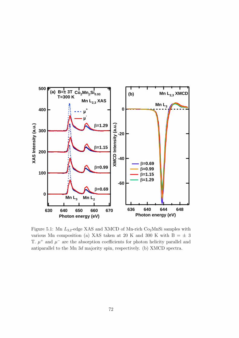
500
400
300
200
100
0
670660650640630
XA
S In
tens
ity (
a.u.
)
b=0.69
b=0.99
b=1.15
b=1.29
(a) B=± 3T T=300 K
µ+
µ-
Mn L2,3 XAS
Mn L2Mn L3
Co2MnbSi0.93
Photon energy (eV)
-60
-40
-20
0
648644640636Photon energy (eV)
XM
CD
Inte
nsity
(a.
u.)
b=0.69 b=0.99 b=1.15 b=1.29
(b)
Mn L3
Mn L2,3 XMCD
Figure 5.1: Mn 𝐿3,2-edge XAS and XMCD of Mn-rich Co2MnSi samples with
various Mn composition (a) XAS taken at 20 K and 300 K with B = ± 3
T. 𝜇+ and 𝜇− are the absorption coefficients for photon helicity parallel and
antiparallel to the Mn 3𝑑 majority spin, respectively. (b) XMCD spectra.
72
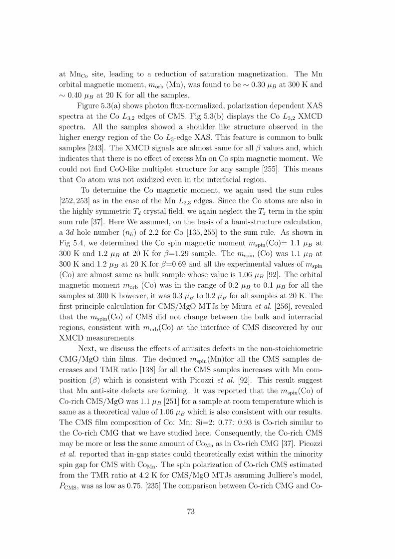
at MnCo site, leading to a reduction of saturation magnetization. The Mn
orbital magnetic moment, 𝑚orb (Mn), was found to be ∼ 0.30 𝜇𝐵 at 300 K and
∼ 0.40 𝜇𝐵 at 20 K for all the samples.
Figure 5.3(a) shows photon flux-normalized, polarization dependent XAS
spectra at the Co 𝐿3,2 edges of CMS. Fig 5.3(b) displays the Co 𝐿3,2 XMCD
spectra. All the samples showed a shoulder like structure observed in the
higher energy region of the Co 𝐿3-edge XAS. This feature is common to bulk
samples [243]. The XMCD signals are almost same for all 𝛽 values and, which
indicates that there is no effect of excess Mn on Co spin magnetic moment. We
could not find CoO-like multiplet structure for any sample [255]. This means
that Co atom was not oxidized even in the interfacial region.
To determine the Co magnetic moment, we again used the sum rules
[252, 253] as in the case of the Mn 𝐿2,3 edges. Since the Co atoms are also in
the highly symmetric 𝑇𝑑 crystal field, we again neglect the 𝑇𝑧 term in the spin
sum rule [37]. Here We assumed, on the basis of a band-structure calculation,
a 3𝑑 hole number (𝑛ℎ) of 2.2 for Co [135, 255] to the sum rule. As shown in
Fig 5.4, we determined the Co spin magnetic moment 𝑚spin(Co)= 1.1 𝜇𝐵 at
300 K and 1.2 𝜇𝐵 at 20 K for 𝛽=1.29 sample. The 𝑚spin (Co) was 1.1 𝜇𝐵 at
300 K and 1.2 𝜇𝐵 at 20 K for 𝛽=0.69 and all the experimental values of 𝑚spin
(Co) are almost same as bulk sample whose value is 1.06 𝜇𝐵 [92]. The orbital
magnetic moment 𝑚orb (Co) was in the range of 0.2 𝜇𝐵 to 0.1 𝜇𝐵 for all the
samples at 300 K however, it was 0.3 𝜇𝐵 to 0.2 𝜇𝐵 for all samples at 20 K. The
first principle calculation for CMS/MgO MTJs by Miura et al. [256], revealed
that the 𝑚spin(Co) of CMS did not change between the bulk and interracial
regions, consistent with 𝑚orb(Co) at the interface of CMS discovered by our
XMCD measurements.
Next, we discuss the effects of antisites defects in the non-stoichiometric
CMG/MgO thin films. The deduced 𝑚spin(Mn)for all the CMS samples de-
creases and TMR ratio [138] for all the CMS samples increases with Mn com-
position (𝛽) which is consistent with Picozzi et al. [92]. This result suggest
that Mn anti-site defects are forming. It was reported that the 𝑚spin(Co) of
Co-rich CMS/MgO was 1.1 𝜇𝐵 [251] for a sample at room temperature which is
same as a theoretical value of 1.06 𝜇𝐵 which is also consistent with our results.
The CMS film composition of Co: Mn: Si=2: 0.77: 0.93 is Co-rich similar to
the Co-rich CMG that we have studied here. Consequently, the Co-rich CMS
may be more or less the same amount of CoMn as in Co-rich CMG [37]. Picozzi
et al. reported that in-gap states could theoretically exist within the minority
spin gap for CMS with CoMn. The spin polarization of Co-rich CMS estimated
from the TMR ratio at 4.2 K for CMS/MgO MTJs assuming Julliere’s model,
𝑃CMS, was as low as 0.75. [235] The comparison between Co-rich CMG and Co-
73

4
3
2
1
0
mS
pin
(µB/M
n) Spin magnetic moment of Mn
300K 20K Sato et al. PRB 2010 at 300K
Co2MnbSi0.93
4
3
2
1
01.21.11.00.90.80.7
b
mO
rbita
l(µ B
/Mn)
Orbital magnetic moment of Mn
300K 20K
Figure 5.2: Mn composition (𝛽) dependence of the Mn spins magnetic moment
(a) and the Mn orbital magnetic moment (b). They have been determined by
using the spin and orbital sum rules [252,253].
74

500
400
300
200
100
0
810800790780770
b=0.69
b=0.99
b=1.15
b=1.29
(a) B=± 3T T=300 K
Co L2,3 XAS
µ+
µ-
Co L2Co L3
Co2MnbSi1.06
XA
S In
tens
ity (
a.u.
)
Photon energy (eV)
-40
-30
-20
-10
0
10
788784780776Photon energy (eV)
b=0.69 b=0.99b=1.15b=1.29
Co L3
Co L2,3 XMCD(b)
XM
CD
Inte
nsity
(a.
u.)
Figure 5.3: Co 𝐿3,2-edge XAS and XMCD of Mn-rich Co2MnSi samples with
various Mn composition (a) XAS taken at 20 K and 300 K with B = ±3
T. 𝜇+ and 𝜇− are the absorption coefficients for photon helicity parallel and
antiparallel to the Mn 3𝑑 majority spin, respectively. (b) XMCD spectra.
75
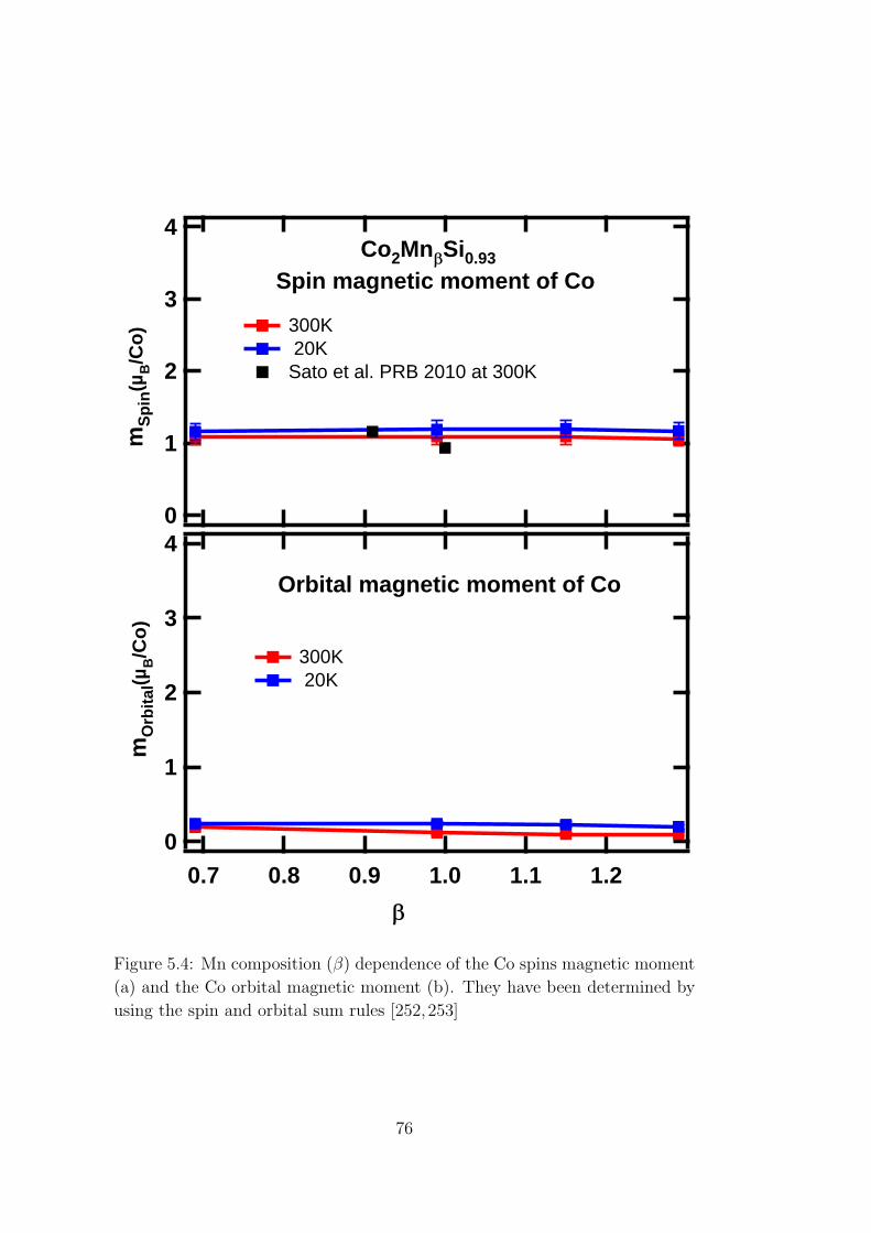
4
3
2
1
0
mS
pin
(µB/C
o)
Spin magnetic moment of Co
300K 20K Sato et al. PRB 2010 at 300K
Co2MnbSi0.93
4
3
2
1
01.21.11.00.90.80.7
b
mO
rbita
l(µ B
/Co)
Orbital magnetic moment of Co
300K 20K
Figure 5.4: Mn composition (𝛽) dependence of the Co spins magnetic moment
(a) and the Co orbital magnetic moment (b). They have been determined by
using the spin and orbital sum rules [252,253]
76

rich CMS can be summarized as follows: (i)the deviation in composition from
2:1:1 for CMG is larger than that for CMS, (ii) the 𝑃CMG of 0.74 (Ref. [261]) is
comparable to the 𝑃CMS of 0.75, [235] and (iii) the experimental 𝑚spin(Co) of
the present XMCD results and the theories for CMS and CMG are reasonably
matching. Importantly, the creation of CoMn antisites in Mn-rich CMS elec-
trodes would be suppressed because a MnCo antisite has a much lower energy
than a CoMn antisite. The suppression of CoMn antisite formation would lead
to a decreased density of gap states around 𝐸𝐹 for Mn-rich CMS. To put it
briefly, CoMn antisites which are harmful to the half-metallicity of CMS would
be suppressed with an increasing Mn composition, resulting in a decreased
density of gap states around 𝐸𝐹 of CMS electrodes. For Mn- rich region, there
is no effect on 𝑚spin(Co) of the composition of Mn because the Co-rich CMS
may be more or less the same amount of CoMn as in Co-rich CMG.
5.3.2 Magnetic properties of Co2Mn𝛽Ge0.38 MTJs as a
function of Mn composition 𝛽
Figure 5.5(a) shows the photon flux-normalized polarization dependent XAS
spectra (𝜇+ and 𝜇−) at the Mn 𝐿3,2 edges (2𝑝3/2,1/2 → 3𝑑 absorption). Fig
5.5(b) displays the Mn 𝐿3,2-edge XMCD (Δ𝜇 = 𝜇+-𝜇−) spectra. Here 𝜇+ and
𝜇− stand for the absorption coefficient for the photon helicity parallel and
antiparallel to the Mn 3𝑑 majority spin. The background subtraction of the
XAS and CMCD spectra are shown in Chapter 2 [see Fig 2.2]. In the XAS
spectra for Mn composition 𝛽 from 0.67 to 1.80, a shoulder-like structure was
observed on the higher energy side of the Mn 𝐿3 peak, and the Mn 𝐿2 peak was
split into a doublet. These features are characteristics observed for Co2MnSi
and Co2MnGe [243]. In the XAS spectra for Mn composition (𝛽) 1.40 and
1.60, showed a Mn2+-like multiplet structure in MnO, in contrast to lower
value of 𝛽. The XAS and XMCD intensities at both 20 K and 300 K showed
𝛽 dependence, that is, XAS and XMCD intensities decreases with 𝛽 = 0.67 to
1.80 at 20 K and 300 K.
By applying the sum rules [252,253], we obtained the spin- and orbital-
magnetic moments of the Mn atom from the XAS and XMCD spectra. We
assumed the contribution of the dipole operator term 𝑇𝑧 in the spin sum rule to
be negligibly small because the Mn site in CMG has 𝑇𝑑 symmetry [37]. Since
there are overlapping regions of 𝐿3 and 𝐿2 due to strong exchange interaction
between the Mn 2𝑝 core hole and the Mn 3𝑑 electrons in Mn 𝐿2,3 XAS and
XMCD, we divided the obtained spin-magnetic moment by a correction factor
0.68 given by Teramura et al. [254]. We assumed, on the basis of a band-
structure calculation, a 3𝑑 hole number (𝑛ℎ) of 4.5 for Mn. [135, 255]. As
77
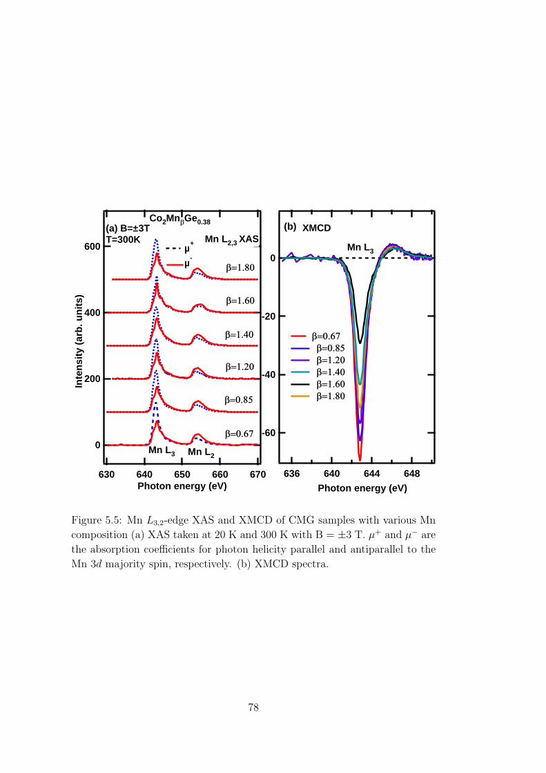
600
400
200
0
670660650640630
b=0.67
b=0.85
b=1.20
b=1.40
b=1.60
b=1.80
Inte
nsity
(ar
b. u
nits
)
(a) B=±3TT=300K Mn L2,3 XAS
Mn L3 Mn L2
Co2MnbGe0.38
µ+
µ-
Photon energy (eV)
-60
-40
-20
0
648644640636
Photon energy (eV)
Mn L3
b=0.67
b=0.85 b=1.20 b=1.40 b=1.60 b=1.80
(b) XMCD
Figure 5.5: Mn 𝐿3,2-edge XAS and XMCD of CMG samples with various Mn
composition (a) XAS taken at 20 K and 300 K with B = ±3 T. 𝜇+ and 𝜇− are
the absorption coefficients for photon helicity parallel and antiparallel to the
Mn 3𝑑 majority spin, respectively. (b) XMCD spectra.
78
shown in Fig 5.6, the deduced spin magnetic moment m𝑠𝑝𝑖𝑛 (Mn) was 2.94 𝜇𝐵
at 300 K and 3.08 𝜇𝐵 at 20 K for 𝛽 =1.2. For 𝛽=1, 𝑚spin (Mn) was nearly
the as same the theoretical value 3.04 𝜇𝐵 for bulk [92]. Also the trend of 𝑚spin
(Mn) with 𝛽 was consistent with theoretical calculation by Picozzi et al. [92]
which predicts the Mn magnetic moment is now coupled antiferromagnetically
at MnCo site, leading to a reduction of saturation magnetization. The Mn
orbital magnetic moment, 𝑚orb (Mn), was found to be 0.3 ∼ 0.2 𝜇𝐵 at 300 K
and 0.40 ∼ 0.3 𝜇𝐵 at 20 K for all the samples.
Figure 5.7(a) shows photon flux-normalized, polarization dependent XAS
spectra at the Co 𝐿3,2 edges of CMG. Fig 5.7(b) displays the Co 𝐿3,2 XMCD
spectra. All the samples showed a shoulder like structure observed in the
higher energy side of the Co 𝐿3-edge XAS. This feature is common to bulk
samples [243]. We could not find CoO-like multiplet structure for any sample
[255]. This means that Co atom was not oxidized even in the interfacial region.
To determine the Co magnetic moment, we again used the sum rules
[252, 253] as in the case to the Mn 𝐿2,3 edges. Since the Co atoms are also in
the highly symmetric 𝑇𝑑 crystal field, we again neglect the 𝑇𝑧 term in the spin
sum rule [37]. Here We assumed, on the basis of a band-structure calculation,
a 3𝑑 hole number (𝑛ℎ) of 2.2 for Co [135, 255] to the sum rule. As shown
in Fig 5.8, we determined the Co spin magnetic moment 𝑚spin(Co)= 1.2 𝜇𝐵
at 300 K and 1.4 𝜇𝐵 at 20 K for 𝛽 =1.2 sample. The 𝑚spin (Co) was 1.3
𝜇𝐵 at 300 K and 1.4 𝜇𝐵 at 20 K for 𝛽=0.67 and all the experimental values
of 𝑚spin(Co) are obviously larger and/or equal to the theoretically predicted
value of 1.06 𝜇𝐵 [91, 92]. For Co-rich region, there is the possibility of the
existence of CoMn because 𝑚spin(Co)=1.5 𝜇𝐵 is larger than 1.06 𝜇𝐵 for Co
at the regular Co site, CoCo. Picozzi et al. [92] investigated theoretically the
effect of antisite defects in CMG and CMS. They reported that 𝑚spin(Co) of
the Co antisites in CMG, CoMn, was 1.35 𝜇𝐵. For Mn-rich region, 𝑚spin(Co) is
almost same as theoretical predicted value, that is, there is no effect of excess
Mn on 𝑚spin(Co). The orbital magnetic moment 𝑚orb (Co) was in the range
of 0.2 𝜇𝐵 to 0.3 𝜇𝐵 for all the samples at 300 K however, it was 0.4 𝜇𝐵 to 0.3
𝜇𝐵 for all samples at 20 K.
Next, we discuss the effects of antisites defects in the non-stoichiometric
CMG/MgO thin films. The deduced 𝑚spin(Mn)for all the CMG samples de-
creases and TMR ratio [138] for all the CMG samples increases with Mn com-
position (𝛽) which is consistent with Picozzi et al. [92]. This result suggest that
Mn anti-site defects are forming. For 𝛽=1.40 and 1.60, 𝑚spin(Mn) decreases
vary rapid because films show oxidation which is clear from XAS spectra. The
deduced 𝑚spin(Co) for all the CMG samples was obviously larger than theoret-
ical value of bulk sample 1.06 𝜇𝐵 and the experimental XMCD value of 1.04
79

4
3
2
1
0
300 K 20 K Theory (for CMG bulk) Asakura et al.,PRB 2010 at 300K
Spin Magnetic Moment of Mn
msp
in(µ
B/M
n)
Co2MnbGe0.38
4
3
2
1
01.81.61.41.21.00.8
Orbital Magnetic Moment of Mn
300 K 20 K Asakura et al.,PRB 2010 at 300K
msp
in(µ
B/M
n)
b
Figure 5.6: Mn composition (𝛽) dependence of the Mn spins magnetic moment
(a) and Co orbital magnetic moment (b). They have been determined by using
the spin and orbital sum rules [252,253].
80
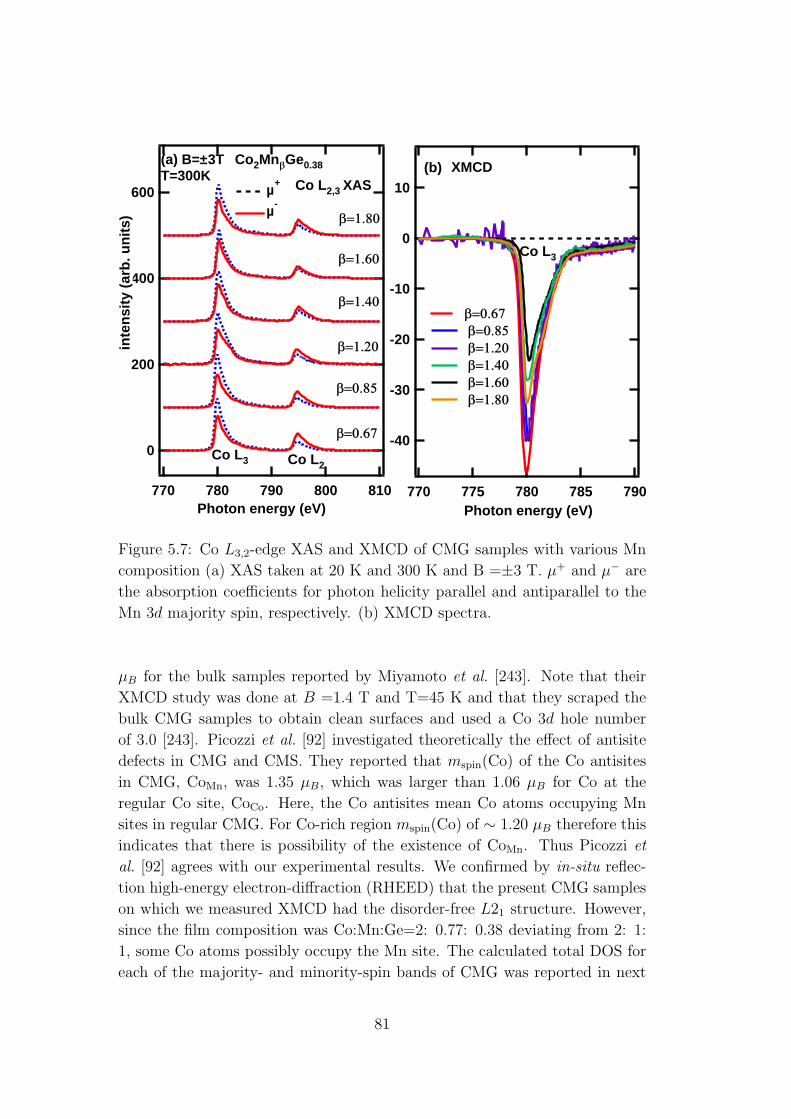
600
400
200
0
810800790780770
b=0.67
b=0.85
b=1.20
b=1.40
b=1.60
b=1.80
inte
nsity
(ar
b. u
nits
)
Co L3 Co L2
Co L2,3 XAS
(a) B=±3TT=300K
µ+
µ-
Co2MnbGe0.38
Photon energy (eV)
-40
-30
-20
-10
0
10
790785780775770Photon energy (eV)
Co L3
b=0.67
b=0.85 b=1.20 b=1.40 b=1.60 b=1.80
(b) XMCD
Figure 5.7: Co 𝐿3,2-edge XAS and XMCD of CMG samples with various Mn
composition (a) XAS taken at 20 K and 300 K and B =±3 T. 𝜇+ and 𝜇− are
the absorption coefficients for photon helicity parallel and antiparallel to the
Mn 3𝑑 majority spin, respectively. (b) XMCD spectra.
𝜇𝐵 for the bulk samples reported by Miyamoto et al. [243]. Note that their
XMCD study was done at 𝐵 =1.4 T and T=45 K and that they scraped the
bulk CMG samples to obtain clean surfaces and used a Co 3𝑑 hole number
of 3.0 [243]. Picozzi et al. [92] investigated theoretically the effect of antisite
defects in CMG and CMS. They reported that 𝑚spin(Co) of the Co antisites
in CMG, CoMn, was 1.35 𝜇𝐵, which was larger than 1.06 𝜇𝐵 for Co at the
regular Co site, CoCo. Here, the Co antisites mean Co atoms occupying Mn
sites in regular CMG. For Co-rich region 𝑚spin(Co) of ∼ 1.20 𝜇𝐵 therefore this
indicates that there is possibility of the existence of CoMn. Thus Picozzi et
al. [92] agrees with our experimental results. We confirmed by in-situ reflec-
tion high-energy electron-diffraction (RHEED) that the present CMG samples
on which we measured XMCD had the disorder-free 𝐿21 structure. However,
since the film composition was Co:Mn:Ge=2: 0.77: 0.38 deviating from 2: 1:
1, some Co atoms possibly occupy the Mn site. The calculated total DOS for
each of the majority- and minority-spin bands of CMG was reported in next
81

4
3
2
1
0
Spin Magnetic Moment of Co 300K 20K Asakura et al.,PRB 2010 at 300K Theory (for CMG bulk)
msp
in(µ
B/C
o)
Co2MnbGe0.38
4
3
2
1
01.81.61.41.21.00.8
300 K 20 K Asakura et al., PRB 2010 at 300K
mO
rbita
l(µ B
/Co)
Orbital Magnetic Moment of Co
b
Figure 5.8: Mn composition (𝛽) dependence of the Co spins magnetic moment
(a) and Co orbital magnetic moment (b). They have been determined by spin
and orbital sum rules [252,253].
82

section and in-gap states were found to exist within the minority-spin gap only
when CoMn existed. The possible existence of CoMn in CMG may lead to a
decrease in the spin polarization. This consideration is consistent with that
the spin polarization of Co-rich CMG estimated from the TMR ratio at 4.2
K for CMG/MgO/CoFe MTJs assuming Julliere’s model, 𝑃CMG, was as low
as 0.74. [261]. However, in Mn-rich region the 𝑚spin(Co) is almost same as
theoretical predicted value.
5.3.3 Mn and Co antisite defects in Co2MnSi and Co2MnGe
(a) Total DOS for defective and Ideal (b) Ideal (c) Defective
Figure 5.9: LDA calculation of antisite defects in Co2MnSi(a) Total DOS for
defective (solid bold line) and ideal (dashed line) Co2MnSi with Mn antisite in
Co2MnSi; majority spin is shown positive and minority spin is negative. The
Mn-antisite PDOS (multiplied by a factor of 3) is also shown (gray shaded
area). Magnetic moments for the ideal(b) and defective (c) systems for the
Mn antisite in Co2MnSi around the defect. Values in bracket denote magnetic
moments for equivalent atoms in Co2MnGe. [92]
Mn antisite defects are most likely to occur in Co2MnSi (Co2MnGe). In
this case the total density of state (DOS) shows a shift of 0.04 eV towards
higher binding energies in the minority spin channel, resulting in a small in-
crease of the spin gap. For this type of antisites disorder the half-metallicity
is maintained. However, the Mn magnetic moment is now coupled antifer-
romagnetically to the Mn antisites, which implies a reduction of saturation
magnetization. Fig 5.9 shows which region close to the defect as compared to
the ideal case, together with the magnetic moments. Since the point defect-
induced changes are efficiently screened by the conduction electrons, only the
83

nearest neighbor spins are affected
(a) Total DOS for defective and ideal (b) Ideal (c) Defective
Figure 5.10: LDA calculation of antisite defects in Co2MnSi(a) Total DOS for
defective (solid bold line) and ideal (dashed line) Co2MnSi with Co antisite in
Co2MnSi. The inset shows the minority DOS at 𝐸𝐹 projected on the different
neighbors (denoted as roman numbers) as one moves away from the Co antisite
defect. Magnetic moments for the ideal (b) and defective (c) systems for the
Co antisite in Co2MnSi around the defect. Values in bracket denote magnetic
moments for equivalent atoms in Co2MnGe [92].
Although Co antisites are theoretically expected to occur in concentra-
tions typically two orders of magnitude smaller than for the case of the Mn
antisite, experimentally these two defects are found to have the same den-
sity [262]. The Mn atom sitting on the Co position leads to a sharp peak in
the electron DOS located in proximity to the Fermi level [see Fig. 5.10 (a)] and
therefore destroys the half-metallicity. The calculated spin polarization for the
case presented in Fig 5.10 (a) is as low as 6%. The defect-induced states at the
Fermi level are spatially localized, as shown in the inset of Fig 5.10(a). The
analysis of magnetic moment [Fig 5.10(b)-(c)] shows that in the case of an Co
antisite defect the magnetic moments remain virtually unchanged and and are
couple ferromagnetically to the surrounding Co spins.
5.3.4 Atom exchange in Co2MnSi and Co2MnGe
Let us now discuss on atomic interchanges and consider Mn-Co exchange;
this defect can also be viewed as the sum of two different Mn and Co atomic
antisites that tend to aggregate. This defect shows a comparatively high for-
mation energy. However, this is of the same order of magnitude as the sum
of the separated defects (Mn and Co antisites) - which might show that point
84
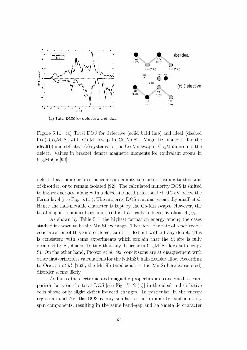
(a) Total DOS for defective and ideal
(b) Ideal
(c) Defective
Figure 5.11: (a) Total DOS for defective (solid bold line) and ideal (dashed
line) Co2MnSi with Co-Mn swap in Co2MnSi. Magnetic moments for the
ideal(b) and defective (c) systems for the Co-Mn swap in Co2MnSi around the
defect. Values in bracket denote magnetic moments for equivalent atoms in
Co2MnGe [92].
defects have more or less the same probability to cluster, leading to this kind
of disorder, or to remain isolated [92]. The calculated minority DOS is shifted
to higher energies, along with a defect-induced peak located -0.2 eV below the
Fermi level (see Fig. 5.11 ), The majority DOS remains essentially unaffected.
Hence the half-metallic character is kept by the Co-Mn swaps. However, the
total magnetic moment per unite cell is drastically reduced by about 4 𝜇𝐵.
As shown by Table 5.1, the highest formation energy among the cases
studied is shown to be the Mn-Si exchange. Therefore, the rate of a noticeable
concentration of this kind of defect can be ruled out without any doubt. This
is consistent with some experiments which explain that the Si site is fully
occupied by Si, demonstrating that any disorder in Co2MnSi does not occupy
Si. On the other hand, Picozzi et al. [92] conclusions are at disagreement with
other first-principles calculations for the NiMnSb half-Heusler alloy. According
to Orgassa et al. [263], the Mn-Sb (analogous to the Mn-Si here considered)
disorder seems likely.
As far as the electronic and magnetic properties are concerned, a com-
parison between the total DOS [see Fig. 5.12 (a)] in the ideal and defective
cells shows only slight defect induced changes. In particular, in the energy
region around 𝐸𝐹 , the DOS is very similar for both minority- and majority
spin components, resulting in the same band-gap and half-metallic character
85

Table 5.1: Formation energy (in eV) and total magnetic moments (in Bohr
magnetons) for the different defects in Co2MnGe and Co2MnSi hosts [92].
Δ𝐸Co2MnSi 𝑀tot(Co2MnSi) Δ𝐸Co2MnGe 𝑀tot(Co2MnGe)
Co antisite 0.80 38.01 0.84 38.37
Mn antisite 0.33 38.00 0.33 38.00
Co-Mn swap 1.13 36.00 1.17 36.00
Mn-Si swap 1.38 40.00 – –
(a) Total DOS for defective and ideal
(b) Ideal
(c) Defective
Figure 5.12: (a) Total DOS for defective (solid bold line) and ideal (dashed line)
Co2MnSi with Mn-Si swap in Co2MnSi. Magnetic moments for (b) ideal and
(c) defective systems for the Mn-Si swap in Co2MnSi around the defect [92].
as for the pure bulk. As a result, the Mn-Si exchange systems illustrate a total
magnetic moment equal to that of the ideal system. This is consistent with
the atomic magnetic moments shown in Fig. 5.12 (b)-(c): within 0.04 𝜇𝐵, the
defect only results in a exchange between the Mn and Si magnetic moments.
Again, this illustrates that the first coordination shell, which in this case is ac-
curately the same as the one in the bulk for both the exchanged atoms, is the
most appropriate in the formation of the bonds, local charge and spin-density
rearrangement, and resulting magnetic moments [92].
5.3.5 Comparison between Co2MnSi and Co2MnGe
In order to compare the behavior of the defects considered in stoichiometric
CMS and CMG, Picozzi et al. [92] report in bracket in Figs. 5.9, 5.10, and
5.11 the value of the atomic magnetic moments in the region around the defect
site. There are two different kinds of hosts which globally show a very similar
behavior in terms of magnetic moments, suggesting that in the determination
86

of the magnetic properties the larger lattice constant or the smaller minority
band gap of the Ge-based compound are not really relevant. The most sensible
differences are shown quantitatively by the Co-antisite case: there is about a
0.4 𝜇𝐵 difference between the total magnetic moments in stoichiometric CMS
and CMG (See Table 5.1). Figure 5.10 demonstrates that this difference is
almost entirely due to differences in the central Co antisite, which changes
from about 20.9 𝜇𝐵 in stoichiometric CMS to about 21.4 𝜇𝐵 in stoichiometric
CMG, due to a very small difference in the energy position (<0.05 eV) of the
defect-induced peak with respect to 𝐸𝐹 [92].
From first principle calculation the DOS with respect to 𝐸𝐹 - and the
related energy position of the conduction-band minimum in the minority-spin
component- is very similar: for both stoichiometric CMS and CMG, the peak
is basically coincident with 𝐸𝐹 in the case of the Co antisite, whereas it lies
at about 20.2 eV in the case of the Co-Mn exchange. Except for very small
differences that can be traced back to differences in the ideal bulk hosts [264],
the calculated DOS for antisite and exchange defects in stoichiometric CMG
are not shown, due to very similar behavior to stoichiometric CMS.
5.3.6 Formula unit composition model for nonstoichio-
metric, Ge-deficient Co2Mn𝛽Ge0.38 films
We now discuss possible defects induced in the prepared nonstoichiometric,
Ge-deficient Co2Mn𝛽Ge0.38 films. Note that the Co:Ge ratio in the prepared
CMG films was 2:0.38, i.e., the Ge ratio was strongly deficient with respect to
the Co ratio. According to the theoretically predicted formation energies of
various kinds of defects for Co2MnSi [92, 249], with the assumption that the
relative magnitude of these formation energies for Co2MnGe is essentially the
same as that for Co2MnSi, we introduce a formula unit composition model for
strongly Ge-deficient CMG films with 𝛽 < 1.62 as Co2[Mn1−𝑥Co𝑥][Ge1−𝑦Mn𝑦],
where [Mn1−𝑥Co𝑥] and [Ge1−𝑦Mn𝑦] represent the nominal Mn and Ge sites,
respectively. The detailed reasons for this model are as follows: For Ge sites,
MnGe antisites, where a Ge site is replaced with a Mn atom, are likely to
be induced because a MnGe antisite has much lower formation energy than a
vacancy at a Ge site and a CoGe antisite [249]. Thus, Ge sites are fully occupied
by the normal Ge atoms and MnGe antisites. For Mn sites, CoMn antisites are
likely to be induced because a CoMn antisite has lower formation energy than
a vacancy at a Mn site [249]. Thus, the normal Mn atoms and CoMn antisites
should occupy Mn sites.
For 𝛽 > 1.62, MnCo antisite should be assumed in addition to MnGe
antisite because of the increased Mn composition with respect to the Co com-
87

position. Indeed, a MnCo antisite has much lower formation energy than a
vacancy at the Co site. Thus, our formula unit composition model for 𝛽 >
1.62 is [Co2−𝑥Mn𝑥][Mn][Ge1−𝑦Mn𝑦].
The Co:Mn:Ge ratio in the above models must be also equal to that in the
representation of Co2Mn𝛽Ge0.38 with a given 𝛽 value. From this requirement,
the values of 𝑥 and 𝑦 are determined. The details are as follows. For 𝛽 <
1.62, the formula unit (f.u.) composition model is Co2[Mn1−𝑥Co𝑥][Ge1−𝑦Mn𝑦].
In this model, the number of Co atom is (2+x), Mn atom is (1-x+y) and Ge
atom is (1-y) for a formula unit. The ratio of Co atom, Mn atom and Ge atom
must satisfy the relation of Co : Mn : Ge = 2: 𝛽 : 0.38. Thus, we obtain
the following relations, (2+𝑥) : (1-𝑥+𝑦) : (1-𝑦) = 2 : 𝛽 : 0.38. From these
relations we get two equations, (2+𝑥) : (1-𝑥+𝑦) = 2 : 𝛽, (2+𝑥) : (1-𝑦) = 2 :
0.38 or (1-𝑥+𝑦) : (1-𝑦) = 𝛽 : 0.38.
There are two unknown parameters, 𝑥 and 𝑦, and two equations. So,
the values of 𝑥 and 𝑦 can be determined by these two equations. However, we
must note that the 𝑥 and 𝑦 should be larger than 0 (𝑥, 𝑦 > 0)
For 𝛽 > 1.62, the formula unit model is [Co2−𝑥Mn𝑥][Mn][Ge1−𝑦Mn𝑦]. In
this model, the number of Co atoms per f.u. is (2-𝑥), that of Mn atoms is
(1+𝑥+𝑦) and that of Ge atoms is (1-𝑦). So, Co : Mn : Ge = (2-𝑥) : (1+𝑥+𝑦)
: (1-𝑦) = 2 : 𝛽: 0.38. Similarly, the two parameters 𝑥 and 𝑦 are determined
by two equations, (2-𝑥) : (1+𝑥+𝑦) = 2 : 𝛽 and (2-𝑥) : (1-𝑦) = 2 : 0.38 or
(1+𝑥+𝑦) : (1-𝑦) = 𝛽 : 0.38. Table 5.2 shows the formula unit compositions
(or chemical compositions) for nonstoichiometric, Ge -deficient Co2Mn𝛽Ge0.38films with various 𝛽 values provided by the models
Table 5.2: Formula unit compositions (chemical compositions) for nonstoichio-
metric Co2Mn𝛽Ge0.38 films according to the models..
𝛽 Formula unit model 𝑥 𝑦 Formula unit composition
0.67 Co2[Mn1−𝑥Co𝑥][Ge1−𝑦Mn𝑦] 0.623 0.502 Co2[Mn0.377Co0.623] [Ge0.498Mn0.502]
0.85 Co2[Mn1−𝑥Co𝑥][Ge1−𝑦Mn𝑦] 0.477 0.529 Co2[Mn0.523Co0.477] [Ge0.471Mn0.529]
1.03 Co2[Mn1−𝑥Co𝑥][Ge1−𝑦Mn𝑦] 0.346 0.554 Co2[Mn0.654Co0.346] [Ge0.446Mn0.554]
1.2 Co2[Mn1−𝑥Co𝑥][Ge1−𝑦Mn𝑦] 0.235 0.575 Co2[Mn0.765Co0.235] [Ge0.425Mn0.575]
1.4 Co2[Mn1−𝑥Co𝑥][Ge1−𝑦Mn𝑦] 0.116 0.598 Co2[Mn0.884Co0.116][Ge0.402Mn0.598]
1.6 Co2[Mn1−𝑥Co𝑥][Ge1−𝑦Mn𝑦] 0.010 0.618 Co2[Mn0.990Co0.010][Ge0.382Mn0.618]
1.8 [Co2−𝑥Mn𝑥][Mn][Ge1−𝑦Mn𝑦] 0.086 0.636 [Co1.914Mn0.086]Mn[Ge0.364Mn0.636]
This model provides formula units ranging from Co2[Mn0.377Co0.623] [Ge0.498Mn0.502]
(where 𝑥 is 0.62 ) for Co2Mn0.67Ge0.38 to Co2[Mn0.884Co0.116][Ge0.402Mn0.598]
(where 𝑥 is 0.12) for Co2Mn1.40Ge0.38. Even at 𝛽 = 1.03, for which the Co:Mn
ratio is close to 2:1, the model provides a formula unit of Co2[Mn0.654Co0.346]
88

[Ge0.446Mn0.554] that features a still high 𝑥 value of 0.35 for Co2Mn1.03Ge0.38.
This is because the Ge ratio is strongly deficient for Co2Mn𝛽Ge0.38. The similar
way we can also explain for Co2Mn𝛽Si0.88.
Thus, it was shown that the formula unit model based on the formation
energies of various kinds of defects reasonably explains the observed depen-
dence of saturation magnetization (𝜇𝑠) on 𝛽 [138]. This finding supports our
interpretation that the Mn composition dependence of the TMR ratio and
spin magnetization observed universally for CMG-MTJs is due to suppressed
minority-spin gap states around 𝐸𝐹 which are caused by the decreased CoMn
sites in Mn-rich CMG electrode. As we know that Picozzi et al. [92] works
for stoichiometric only down to Mn0.9 and Ge0.9. Since we have seen that our
result from 𝛽=0.67 to 𝛽=1 is consistent with Picozzi et al. [92] and similar ten-
dency was observed by Yamamoto et al. [138] for 𝛽=0.67 to 𝛽=1.40, thus, our
results support to Picozzi et al. [92] as well as Yamamoto et al. [138]. Hence
we justify that chemical stoichiometry and non-stoichiometry CMS and CMG
samples match with stoichiometric (only down to Mn0.9 and Ge0.9) as predicted
by Picozzi et al. [92] and the non-stoichiometry by Yamamoto et al. [138] and
thus my experimental results open the door for theoretician to investigate the
electronic structures of non-stoichiometric, Ge-deficient Co2Mn𝛽Ge0.38 from
first-principles.
5.4 Conclusion
We have studied the magnetic and electronic states of the CMS/MgO and
CMG/MgO interfaces by means of XMCD. By investigating the 𝛽 dependence
of XMCD of CMS/MgO and CMG/MgO interfaces. We obtained that the de-
duced 𝑚spin(Mn) for all the CMS samples decreases with Mn composition (𝛽)
which is consistent with Picozzi’s calculations which predicts the Mn magnetic
moment is now coupled antiferromagnetically at MnCo site, leading to a reduc-
tion of saturation magnetization. The deduced 𝑚spin(Co) for all the samples
was almost equal to a theoretical value of 1.06 𝜇𝐵. The Co spin magnetic mo-
ment was almost constant of the composition of Mn. Thus the Co-rich CMS
may be more or less the same amount of CoMn as in Co-rich CMG.
The deduced 𝑚spin(Mn) for all the CMG samples decreases with Mn
composition (𝛽), which is also consistent with Picozzi et al.’s calculations which
predicts the Mn magnetic moment is now coupled antiferromagnetically at
MnCo site, leading to a reduction of saturation magnetization. However, the
deduced 𝑚spin(Co) for all the CMG samples was also obviously larger and/or
equal to a theoretical bulk value of 1.06 𝜇𝐵. For Co-rich region, there is the
possibility of the existence of CoMn because 𝑚spin(Co)=1.5 𝜇𝐵 is larger than
89

1.06 𝜇𝐵 for Co at the regular Co site, CoCo. For Mn-rich region, 𝑚spin(Co) is
almost same as theoretical predicted value.
90

Chapter 6
Summary and Outlook
In this thesis, we have presented the results of soft x-ray spectroscopic
studies of TiO2-DMSs, BiFe3-multiferroic and Co2Mn𝑍-Heusler alloys. For
the Co-doped TiO2 thin film, present experimental results suggest that carrier-
mediated FM mechanism plays a key role to achieve high-𝑇C. For the TiO2-
DMS thin films, we find that the doped TM ions are in a Co2+ high-spin
state at surface. However, in bulk region the doped TM ions are in a Co2+
mixed-spin state.
In Chapter 3, to clarify the origin of the room-temperature ferromag-
netism of the Ti1−𝑥Co𝑥O2−𝛿 system, we have performed XAS, XMCD on rutile-
type Ti1−𝑥Co𝑥O2−𝛿 at the Co 𝐿2,3 edges (both in the TEY and TFY mode).
These results represent that the high temperature ferromagnetism is origi-
nated from the Co2+ atoms, most probably charge carriers induce the ferro-
magnetism. The magnetic moment of the Co ions as long as 0.82-2.25 𝜇𝐵/Co
was first observed by the bulk sensitive TFY method. The magnetic moment
value deduced with the TEY mode ( 0.15-0.24 𝜇𝐵/Co) indicates the presence
of a magnetically dead layer of ∼ 5 nm thickness on the sample surface. The
results give a strong evidence for intrinsic ferromagnetism in this compound
and unveil deep underlying physics of the room temperature ferromagnetism,
and will contribute to the implementation of semiconductor spintronics devices
operable at room temperature.
we have also provided experimental evidence for carrier-induced ferro-
magnetism of cobalt-doped anatase TiO2 thin films using XMCD at the Co
𝐿2,3 edges in both the TEY and TFY modes. The large magnetic moment of
the Co ions, 0.6-2.4 𝜇𝐵/Co, was observed by the bulk-sensitive TFY method.
The carrier-induced origin of ferromagnetism at room-temperature in anatase
Ti1−𝑥Co𝑥O2−𝛿 is confirmed on the basis of the element-specific XMCD study
at the surface as well as in bulk. In the bulk-sensitive TFY mode, the position
of Co2+ atoms seems to be displaced from the Ti4+ sites, resulting in more
91

random crystal fields. Good agreement is demonstrated not only in magneti-
zation and AHE but also in the magnetic field dependences of XMCD. The
magnetic moment values deduced with the TEY mode was < 0.3 𝜇𝐵/Co, in-
dicating the presence of a magnetically dead layer of ∼ 5 nm thickness at the
sample surfaces.
In Chapter 4, we have performed XAS and the XMCD measurements
of epitaxial BFCO thin films prepared by chemical solution deposition on
LaAlO3(001) substrate, which exhibit ferromagnetism at 300 K. The XAS
and XMCD line shape of Fe ions in BFCO thin films are independent of the
magnetic field, indicating that the ferromagnetism originates from the anti-
ferromagnetic coupled Fe3+ ions at the 𝑂ℎ and 𝑇𝑑 sites and ferromagnetism
behavior in the BFCO thin films is mainly arose from 𝛾-Fe2O3 like species as
a secondary phase (i.e. ferromagnetism behavior in the BFCO thin films is
mainly arose from extrinsic behavior). The magnetic moment of Fe increases
with Co content up to 20% and after that it decreases. The Co ions are in
the trivalent high-spin states and are largely paramagnetic . The Co magnetic
moment is nearly independent of Co content, unlike Fe, and the peak at 20%
Co has only a minor influence. Surface Fe ions in these films also showed a
significant enhancement compared with a bulk sample probed by XMCD. This
may be because of XMCD can detect the thickness of ∼ 5nm on the surface
and therefore detected larger magnetization than SQUID data.
In Chapter 5, We studied the magnetic and electronic states of Co2Mn𝛽Si0.88/MgO
magnetic tunnel junctions by CMS film-composition (𝛽) dependent XMCD
measurements. The XAS and XMCD spectral shapes for these samples were
similar to those for bulk CMS and neither the Mn nor Co atoms were oxi-
dized. By investigating the 𝛽 dependence of XMCD and magnetic moments of
CMSs, we have revealed that the magnetic states of the Mn and Co atoms at
interfacial region, facing to the MgO barrier. We obtained that the deduced
𝑚spin(Mn) for all the CMS samples decreases with Mn composition (𝛽) which
is consistent with Picozzi’s calculations which predicts the Mn magnetic mo-
ment is now coupled antiferromagnetically at MnCo site, leading to a reduction
of saturation magnetization. The deduced 𝑚spin(Co) for all the samples was
almost equal to a theoretical value of 1.06 𝜇𝐵. The Co spin magnetic moment
was almost constant of the composition of Mn. Thus the Co-rich CMS may
be more or less the same amount of CoMn as in Co-rich CMG.
We studied the magnetic and electronic states of Co2Mn𝛽Ge0.38/MgO
magnetic tunnel junctions by CMG film-composition (𝛽) dependent XMCD
measurements. The XAS and XMCD spectral shapes for these samples were
similar to those for bulk CMG and and neither the Mn nor Co atoms were
oxidized. The deduced 𝑚spin(Mn) for all the CMG samples decreases with
92

Mn composition (𝛽), which is also consistent with Picozzi et al.’s calculations
which predicts the Mn magnetic moment is now coupled antiferromagnetically
at MnCo site, leading to a reduction of saturation magnetization. However, the
deduced 𝑚spin(Co) for all the CMG samples was also obviously larger and/or
equal to a theoretical bulk value of 1.06 𝜇𝐵. For Co-rich region, there is the
possibility of the existence of CoMn because 𝑚spin(Co)=1.5 𝜇𝐵 is larger than
1.06 𝜇𝐵 for Co at the regular Co site, CoCo. For Mn-rich region, 𝑚spin(Co) is
almost same as theoretical predicted value.
Finally, future prospects of spintronics research are mentioned. Based
on a number of theoretical predictions [9, 265], room-temperature ferromag-
netism has been reported in DMS such as the TiO2-, ZnO-, and GaN-based
DMSs [183, 266–268]. In particular, there is growing interest in systems with
native defects such as DMS nano-particles because DMS nano-particles have
several advantages for the practical DMS as follows. Firstly, DMS nano-
particles have high surface-to-volume ratios and are amenable for surface mod-
ifications, which could be used to alter the electronic configuration [269]. Ac-
cording to the recent theoretical calculation of the DMS nano-particles [269],
the valence states of TM ions in the DMS nano-particles are changed by the
surface defects and thus magnetic interaction between the substitutional TM
ions changes. Secondly, detrimental substrate effects, such as mismatches in
thermal conductivities and lattice constants, are much weaker in the nano-
particles growth. Thirdly, the processing conditions used in nano-particles
synthesis are often different from thin-film deposition conditions, offering op-
portunities to tune the structural and chemical characteristics, which were
shown to exert significant influence on the magnetism of DMSs [270]. Finally,
DMS nano-particles are potential nano scale building blocks for spintronics
if they show robust magnetism [271]. Subsequently a number of experiments
on DMS nano-particles such as ZnS [272], ZnO [272] and TiO2 [176] revealed
ferromagnetic properties. In this thesis, we have indicated that the TM ions
in the DMS thin-films show small magnetization at surface, which are due
to surface dead layer and show large magnetization in bulk, and they play a
crucial role in ferromagnetism. The present work suggests that not only the
magnetic dopants themselves but also the defects are important to understnad
ferromagnetism of the DMS nano-particles. Hence, systematic study of the ef-
fects of particle’s size, shape, and surface structure on the magnetic properties
of various DMSs nano-particles such as ZnS, TiO2 and ZnO are desired.
In this thesis, we have also indicated that the Co-doped BiFeO3 (BFCO)
thin-films by chemical solution deposition method which show strong ferro-
magnetism at room-temperature. In this material, the most of the ferromag-
netism comes from 𝛾-Fe2O3 nanoparticles. Since BCFO is strong ferroelectric
93
so we may consider that BFCO/𝛾-Fe2O3 forms a nanocomposite and can show
a strong magnetoelectric coupling response. Hence, systematic study of the
magnetoelectric coupling response of various type of composites are necessary.
In addition to DMSs, we have studied the electronic and magnetic struc-
ture of the Heusler alloys. We find that XMCD measurements is a very pow-
erful tool to investigate the electronic configuration of these alloys. Spin-
resolved photoemission studies would also be desirable to directly observe the
half-metallic nature of Heusler alloys. We hope that the present work will pro-
mote soft x-ray spectroscopy on DMS’s and leads to further understandings of
physics of diluted magnetic semiconductor.
94
Acknowledgments
I would like to thank my sincere gratitude to my thesis supervisor Prof.
Atsushi Fujimori for his advice, guidance, patience and tremendous help with
during the project. His constant encouragement, and freedom to work with
anything and at any time made my life much easier and it helped me to work
more efficiently. It is a great honor for me to have been a part of his team at the
diluted magnetic semiconductor (DMS) laboratory, the successful completion
of the work has been only possible due to their excellent guidance, meticulous
observation and critical analysis.
I would also like to express my great thanks to Dr. Teppei Yoshida.
His valuable advices were indispensable to this work. I have learned a lot
from his energetic action and thoughtfulness. I would like to say my special
thanks to Dr. Takashi Kataoka and Mr.Yuta Sakamoto who have introduced
me the enchanted world of DMS. They always helped me and gave spurs to
me when I was in trouble and was ready to give up. They have always been
taking care of me throughout my PhD. I have been stimulated from his strong
will and energetic attitude to the work. I would also like to say my special
thanks to Dr. Walid Meleab and Mr. Shin-ichi Aizaki who were providing me
continuous encouragement. They always helped and took care of me. I have
been stimulated from their strong will and energetic attitude to the work. His
valuable advice was indispensable to this work.
The experiment at BL-16A of Photon Factory was supported by a number
of people, Prof. Tsuneharu Koide, Prof. Kenta Amemiya, and Dr. Daisuke
Asakura. I would like to thank their valuable technical support during the
beamtime. The experiment at SPring-8 was supported by a number of people.
I would like to thank the members : Dr. Yukiharu Takeda, Dr. Takuo Ohkochi,
Dr. Kouta Terai, Dr. Shin-ichi Fujimori, Dr. Tetsuo Okane, Dr. Yuji Saitoh
and Prof. Hiroshi Yamagami. The experiment at Taiwan Light Source were
supported by a number of people. I would also like to thank the members :
Mr. Fan-Hsiu Chang, Dr. Hong-Ji Lin, Prof. Di-Jing Huang and Prof. C. T.
Chen. I really appreciate their helpful technical support during the beamtime.
I would like to express my great thanks to Dr.H. Toyosaki, Dr.Y. Ya-
95

mada, Prof. T. Fukumura and Prof.M. Kawasaki. They provided us with the
high-quality samples of the Co-doped rutile TiO2 as well as Co-doped anatase
TiO2 thin films and warm encouragement. I am also very thankful to Dr.Y.
Nakamura, Prof.M. Azuma and Prof. Y. Shimakawa for providing us the inter-
esting samples BiFeO3:Co thin films and valuable discussions. I am also very
thankful to Dr. T. Ishikawa and Prof. M. Yamamoto for providing us the in-
teresting samples Co2MnSi and Co2MnGe thin films and valuable discussions.
I would like to thank Dr. Hirohiko Okamoto and Dr. Tohru Yamanouchi
for the guidance for the SQUID magnetometer and his support during the
magnetization measurements.
I am grateful to the members of Fujimori Group : Dr. T. Kadono,
Mr. Shin-ichiro Ideta, Mr.Viendra Kumar Verma, Mr. Keisuke Ishigami,
Mr. Leo Cristobal C Amblode II, Mr.Yo Yamazaki, Mr. Ichiro Nishi, Mr.
Wataru Uemura, Mr. Goro Shibata, Mr. Hakuto Suzuki and Mr. Takayuki
Harano. Ms. Miki Ueda, Ms. Kaoru Fukutomi, and Ms. Emiko Murayama for
their supports. Especially, Mr. Keisuke Ishigami, Mr. Yo Yamazaki, and
Mr. Ichiro Nishi helped me on many scenes in the research and their energetic
attitudes toward the research have always encouraged me. I have to express
my great thanks Mr. Virendra Kumar Verma who is a partaker of my joys
and sorrows in the life as a researcher. I have been stimulated from his strong
mind and brilliance. I was really glad to go through my life in Fujimori-group
with them. Not only they gave me valuable discussions but also helped me to
enjoy my life in Japan.
I would also like to greatly acknowledge the financial support from the
Ministry of Education, Culture, Sports, Science and Technology (MEXT),
Japan.
My stay in Tokyo makes a lot of friends who shared with me everything
and a lot of discussions. List is very long, in no particular order Dr. Md.
Rizwan, Dr. Md. Waseem Akhtar, Dr. Md. Rafi, Dr. Zainul aabdin Khan,
Dr. Gautam Singh, Dr. Anand Prakash, and Mr. Deepu. I would also like
to thank my friends Er. Praveen Kumar, Er. Vipin Tripathi, Er. Harish Kr.
Gangwar, Er. Ranbir Singh, Er. Prashant Gupta, Dr. Vinod Kumar, Mrs.
Alka Gupta and many more (sorry if I miss someone’s name!) who made my
days at University of Tokyo really enjoyable and cheerful.
Finally I would like to have an exclusive thanks to my family, especially
my parents for their love, support, and constant guidance and care throughout
my life. May God bless you two; my mom and dad, as I could never ever
thought of any two persons sacrificing and dedicating themselves to my success
so trustworthy and humbly and without any expectation what so ever. I wish
I could return all these kindness. My brother, sisters, sister-in-law, brother-
96

in-law and my consort (Ms. Chandrakiran Singh) I thank them very much for
your encouragement, company and support throughout the years. I will never
forget the support of Mr. D. R. Singh (elder brother), without his support it
would not have been possible to complete my Ph.D. He is really superb and
fantastic with his sense of humor. This kind of brother is born only once upon
a time. I still have to thank the rest of my friends, whom I can not name all,
but I am sure I owe them a lot for all the good times together.
Tokyo, June 2011
Vijay Raj Singh
97

References
[1] T. Dietl and H. Ohno, Materials Today 9, 18 (2006).
[2] T. Dietl, Semicond. Sci. Technol. 17, 377 (2002); J. K. Furdyna, J. Appl.
Phys 64, R29 (1988).
[3] H. Ohno, Science 281, 951 (1998).
[4] D. Ferrand, J. Cibert, A. Wasiela, C. Bourgognon, S. Tatarenko, G. Fish-
man, T. Andrearczyk, J. Jaroszynski, S. Kolesnik, T. Dietl, B. Barbara,
and D. Dufeu, Phys. Rev. B 63, 085201 (2001).
[5] A. Haury, A. Wasiela, A. Arnoult, J. Cibert, S. Tatarenko, T. Dietl, and
Y. Merle d’Aubigne, Phys. Rev. Lett. 79, 511 (1997).
[6] N. Samarth, Nature Mater. 6, 403 (2007).
[7] S. Kuroda, N. Nishizawa, K. Takita, M. Mitome, Y. Bando, K. Osuch,
and T. Dietl, Nature Mater. 6, 440 (2007).
[8] T. Jungwirth, K. Wang, J. Masek, K. Edmonds, J. Konig, J. Sinova, M.
Polini, N. Goncharuk, A. MacDonald, M. Sawicki, R. Campion, L. Zhao,
C. Foxon, and B. Gallagher, Phys. Rev. B 72, 165204 (2005).
[9] T. Dietl, H. Ohno, F. Matsukura, J. Cibert, and D. Ferrand, Science 287,
1019 (2000).
[10] J. M. D. Coey, M. Venkatesan, and C. B. Fitzgerald, Nature Mater. 4,
173 (2005).
[11] D. H. Kim, J. S. Yang, K. W. Lee, S. D. Bu, T. W. Noh, S.-J. Oh, Y.-W.
Kim, J.-S. Chung, H. Tanaka, H. Y. Lee, and T. Kawai, Appl. Phys. Lett.
81, 2421 (2002).
[12] A. Chambers, Surf. Sci. Rep. 61, 345 (2006).
[13] Y. J. Lee, M. P. de Jong, and R. Jansen, Appl. Phys. Lett. 96, 082506
(2010).
98

[14] G. Karczewski, J. Supercond. 16, 55 (2003).
[15] H. Saito, V. Zayets, S. Yamagata, and K. Ando, Phys. Rev. Lett. 90,
207202 (2003).
[16] T. Story, R. R. Galazka, R. B. Frankel and P. A. Wolff, Phys. Rev. Lett.
56, 777 (1986).
[17] H. Ohno, H. Munekata, T. Penney, S. von Molnar, and L. L. Chang Phys.
Rev. Lett. 68, 2664 (1992).
[18] H. Ohno, A. Shen, F. Matsukura, A. Oiwa, A. Endo, S. Katsumoto, and
Y. Iye, Appl. Phys. Lett. 69, 363 (1996).
[19] S. Sonoda, S. Shimizu, T. Sasaki, Y. Yamamoto, and H.J. Hori, J.
Cryst.Growth 237, 1358 (2002).
[20] S. E. Park, H.-J. Lee, Y. C. Cho, S.-Y. Jeong, C. R. Cho, and S. Cho,
Appl. Phys. Lett 80, 4187 (2002).
[21] N. Theodoropoulou, A. F. Hebard, M. E. Overberg, C. R. Abernathy,
and S. J. Pearton, S. N. G. Chu, and R. G. Wilson, Phys. Rev. Lett. 89,
107203 (2002).
[22] X. Chen, M. Na, M. Cheon, S. Wang, H. Luo, B. D. McCombe, X. Liu,
Y. Sasaki, T. Wojtowicz, J. K. Furdyna, S. J. Potashnik, and P. Schiffer,
Appl. Phys. Lett. 81, 511 (2002).
[23] Y. D. Park, A. T. Hanbicki, S. C. Erwin, C. S. Hellberg, J. M. Sullivan,
J. E. Mattson, T. F. Ambrose, A. Wilson, G. Spanos, and B. T. Jonker,
Science 295, 651 (2002).
[24] Y. Matsumoto, M. Murakami, T. Shono, T. Hasegawa, T. Fukumura, M.
Kawasaki, P. Ahmet, T. Chikyow, S. Koshihara, and H. Koinuma, Science
291, 854 (2001).
[25] P. Sharma, A. Gupta, K. V. Rao, F. J. Owens, R. Sharma, R. Ahuja, J.
M. Osorio Guillen, B. Johansson, and G. A. Gehring, Nature Mater. 2,
673 (2003).
[26] S. B. Ogale, R. J. Choudhary, J. P. Buban, S. E. Lofland, S. R. Shinde,
S. N. Kale, V. N. Kulkarni, J. Higgins, C. Lanci, J. R. Simpson, N. D.
Browning, S. Das Sarma, H. D. Drew, R. L. Greene, and T. Venkatesan,
Phys. Rev. Lett. 91, 077205 (2003).
99

[27] J. M. D. Coey, A. P. Douvalis, C. B. Fitzgerald, and M. Venkatesan, Appl.
Phys. Lett. 84, 1332 (2004).
[28] J. Philip, A. Punnoose, B. I. Kim, K. M. Reddy, S. Layne, J. O. Holmes,
B. Satpati, P. R. LeClair, T. S. Santos, and J. S. Moodera, Nature Mater.
5, 298 (2006).
[29] Hadis Morkoc and Umit Ozgur, Zinc Oxide: Fundamental Materials and
device technology,(Wily-VCH Press, Berlin, 2009).
[30] P. Kacman, Semiconductor Science and Technology, 16, R25 (2001).
[31] C. Zener, Physical Review, 83, 299 (1951).
[32] C. Zener, Physical Review, 81, 440 (1951).
[33] C. Zener, Phys. Rev. 81, 440 (1950).
[34] A. H. MacDonald, R. Schiffer, and N. Samarth, Nature Mater. 4, 195
(2005).
[35] J. Schliemann, J. Konig, H. Lin, and A. H. MacDonald, Appl. Phys. Lett.
78, 1550 (2001).
[36] T. Jungwirth, J. Sinova, J. Masek, J. Kucera, and A. H. MacDonald, Rev.
Mod. Phys.78, 809 (2006).
[37] A. Kaminski, and S. Das Sarma, Phys. Rev. Lett. 88, 247202 (2002).
[38] M. Berciu, and R. N. Bhatt, Phys. Rev. Lett. 87, 107203 (2001).
[39] G. M. Dalpian, and S. Wei, Phys. Rev. B 73, 245204 (2006).
[40] J. M. D. Coey, Curr. Opin. Solid St. M. 10, 83 (2006).
[41] P. M. Krstajic, F. M. Peeters, V. A. Ivanov, V. Fleurov, K. Kikoin, Phys.
Rev. B 70, 195215 (2004).
[42] M. Yokoyama, H. Yamaguchi, T. Ogawa, and M. Tanaka, J. Appl. Phys.
97, 10D317 (2005).
[43] R. Janisch, P. Gopal, and N. A. Spaldin, J. Phys. Condens. Matter 17,
R657 (2005).
[44] S.A. Chambers, C.M. Wang, S. Thevuthasan, T. Droubay, D.E. Mc-
Cready, A.S. Lea, V. Shutthanandan, and C.F. Windisch Jr, Thin solid
films 418, 197 (2002).
100
[45] H. Toyosaki, T. Fukumura, Y. Yamada, K. Nakajima, T. Chikyow, T.
Hasegawa, H. Koinuma, and M. Kawasaki, Nat. Mater. 3, 221 (2004).
[46] K. Ueno, T. Fukumura, H. Toyosaki, M. Nakano, and M. Kawasaki, Appl.
Phys. Lett. 90, 072103 (2007).
[47] R. Ramaneti, J. C. Lodder, and R. Jansen, Appl. Phys. Lett. 91, 012502
(2007).
[48] T. Yamasaki, T. Fukumura, Y. Yamada, M. Nakano, K. Ueno, T. Makino
and M. Kawasaki, Appl. Phys. Lett. 94, 102515 (2009).
[49] T. Fukumura, H. Toyosaki, and Y. Yamada, Semicond. Sci. Technol. 20,
S103 (2005).
[50] H. Toyosaki, T. Fukumura, Y. Yamada, and M. Kawasaki, Appl. Phys.
Lett. 86,182503 (2005).
[51] S. R. Shinde, S. B. Ogale, J. S. Higgins, H. Zheng, A. J. Millis, V. N.
Kulkarni, R. Ramesh, R. L. Greene, and T. Venkatesan, Phys. Rev. Lett.
92, 166601 (2004).
[52] J.-Y. Kim, J.-H. Park, B.-G. Park, H.-J. Noh, S.-J. Noh, J. S. Yang, D.-H.
Kim, S. D. Bu, T.-W. Noh, H.-J. Lin, H.-H. Hsieh, and C. T. Chen, Phys.
Rev. Lett. 90, 017401 (2003).
[53] K. Mamiya, T. Koide, A. Fujimori, H. Tokano, H. Manaka, A. Tanaka, H.
Toyosaki, T. Fukumura, and M. Kawasaki, Appl. Phys. Lett. 89, 062506
(2006).
[54] S. Lany, H. Raebiger, and A. Zunger, Phys Rev. B 77, 241201(R) (2008).
[55] L. H. Ye, and A. J. Freeman, Phys Rev. B 73, 081304(R) (2006).
[56] J. W. Quilty, A. Shibata, J. -Y. Son, K. Takubo, T. Mizokawa, H.
Toyosaki, T. Fukumura, and M. Kawasaki, Phys. Rev. Lett. 96, 027202
(2006).
[57] Van E. Wood and A. E. Austin, Magnetoelectric interaction phenomena
in crystals, edited by A. J. Freeman and H. Schmid, Gordon and Breach
Science Publishers,(1975).
[58] G. A. Smolenskii and I. E. Chupis, Sov. Phys. Usp. 25, 475, (1982).
[59] I. E. Dzyaloshinsky, J. Exptl. Theor. Phys. (USSR) 37, 881, (1959) [Sov.
Phys. JETP 37, 628(1960)].
101

[60] J. Van Suchtelen, Philips Res. Rep. 27, 28, (1972).
[61] F. Kubel, and H.Schmid, Acta Crystallogr., Sect. B: Struct. Sci. B46,
698, (1990).
[62] C.Michel, J. -M. Moreau, G. D. Achenbach, R. Gerson, W. J. James Solid
State Commun. 7, 701, (1969).
[63] F. Kubel and H.Schmid, Acta Crystallogr., Sect. B: Struct. Sci. B46, 698
(1990).
[64] I. Sosnowska, T. Peterlin-Neumaier and E. Steichele, J. Phys. C: Solid
State Phys. 15, 4835, (1982).
[65] B. Ruette, M S thesis, Virginia Tech (2003).
[66] James R. Teague, Robert Gerson and W. J. James, Solid State Commu-
nications 8, 1073, (1970).
[67] K. Ueda, H. Tabata, and T. Kawai, Appl. Phys. Lett. 79, 988, (2001).
[68] J. Wang, J.B. Neaton, H. Zheng, V. Nagarajan, S.B. Ogale, B. Liu,
D. Viehland, V. Vaithyanathan, D.G. Schlom, U.V. Waghmare, N.A.
Spaldin, K.M. Rabe, M. Wutting, Science 299, 1791, (2003).
[69] M. Fiebig, T. Lottermoser, D. Frohlich, A.V. Goltsev, R.V. Pisarev, Na-
ture 419, 81, (2002).
[70] V. R. Palkar, J. John, and R. Pinto, Appl. Phys. Lett. 80, 1628, (2002).
[71] K. Y. Yun, M. Noda, M. O. Kuyama, Appl. Phys. Lett. 83, 3981, (2003)
.
[72] Y. P. Wang, L. Zhou, M. F. Zhang, X. Y. Cheng, J.-M. Liu, Z.G. Liu,
Appl. Phys. Lett. 84, 1731, (2004).
[73] K. Y. Yun, D. Ricinschi, T. Kanashima, M. Noda, M.Okuyama, Jpn. J.
Appl. Phys., Part 2 43,L647, (2004).
[74] J. Jackson, S. B. Palmer, J. Phys. D: Appl. Phys. 27, 1581, (1994).
[75] I. Sosnowska, M. Loewenhaupt, W. I. F. Davie, R. M. Ibberson, Physica
B 180, 117, (1992).
[76] F. Popov, A. M. Kadomtseva, S. S. Krotov, D. V. Belov, G. P. Vorob’ev,
P. N.Makhov, and A. K. Zvezdin, Low Temperature Physics, 27, 478,
(2001).
102

[77] J.F.Nye, Physical Properties of Crystals,(Oxford university Press, Oxford,
1960).
[78] K. C. Kao, Dielectric Phenomena in Solid,(Elsevier Academic Press, USA,
2004).
[79] W. Cochran, Advan. Phys. 9, 387, (1960); 10, 401, (1961).
[80] P. W. Anderson, Fizika dielektrikov (Akad. Nauk, SSSR, Moscow, (1959).
[81] C. Kittel, Introduction to Solid State Physics, (1976).
[82] A. J. Dekker, Solid State Physics (Macmillan India Limited Press, India,
(2000).
[83] C.S.Smith, Macroscopic Symmetry and Properties of Crystals in Solid
State Physics, Vol 6 (Academic Press New York) (1958).
[84] Y. Nakamura, M. Kawai, M. Azuma, and Y. Shimakawa, Jpn. J. Appl.
Phys. 49, 051501, (2010).
[85] I. E. Dzyaloshinsky, J. Exptl. Theor. Phys. (USSR) 37, 881, (1959).
[86] Van Suchtelen, Philips Res. Rep. 27, 28, (1972).
[87] M. Fiebig, J. Phys. D: Appl. Phys. 38, 123, (2005) .
[88] H. Schmid, Ferroelectrics 162, 317, (1994).
[89] F. Heusler. Verh. Dtsch. Phys. Ges 5, 219, (1903).
[90] P. J. Ziebeck and K. R.A. Webster, Landolt-Bornstein New Series II/19c.
(1986).
[91] I. Galanakis, P. H. Dederichs and N. Papanikolaou, Phys. Rev. B 66,
174429, (2002).
[92] S. Picozzi, A. Continenza and A. J. Freeman, Phys. Rev. B 69, 094423,
(2004).
[93] S. Ishida, S. Fujii, S. Kashiwagi, and S. Asano, J. Phys. Soc. Jpn. 64,
2152 (1995).
[94] S. Picozzi, A. Continenza, and A. J. Freeman, Phys. Rev. B 66, 094421
(2002).
[95] Y. Miura, K. Nagao and M. Shirai, Phys. Rev. B 69, 144413, (2004).
103
[96] P. J. Webster and K. R. A. Ziebeck, Alloys and Compounds of d-Elements
with Main Group Elements - Part 2. H. P. J. Wijn, Landolt-Bornstein,
New Series, Group III, 19/c (Springer, Berlin), (1988).
[97] P. J. Webster, K. R. A. Ziebeck, and K.-U. Neumann, Magnetic Properties
of Metals., New Series, Group III, 32/c (Springer, Berlin), (2001).
[98] J. Pierre, R. V. Skolozdra, J. Alloys Comp. 101, 262, (1997).
[99] J. Tobola, J. Pierre, S. Kaprzyk, R. Skolozdra, and M. Kouacou J. Phys.:
Condens. Matter 10, 1013, (1998).
[100] K. R. A. Ziebeck and P.J. Webster, J. Phys. F 5, 1756, (1975).
[101] P. J. Eewster and R.S. Tebbel, J. Appl. Phys. 39, 471, (1968).
[102] P. J. Eewster, J. Phys. Chem Sol. 32, 1221, (1971).
[103] K. H. J. Buschow and P.G. Van Engen, J. Magn. Mag. Mat. 25, 90,
(1983).
[104] J. Kuebler, A. R. Williams, and C. B. Sommers Phys. Rev. B 28, 4,
(1983).
[105] I. Galanakis, P. H. Dederichs, Half-metallic alloys-Fundamental and Ap-
plications, Lecture Notes in Physics. Springer, (2005).
[106] K. H. J. Buschow and M. Erman, J. Mag. Magn. Mater. 30, 374, (1983).
[107] J. Pierre, R. V. Skolozdra, and Yu. V. Stadnyk, J. Mag. Magn. Mater.
128, 93, (1993).
[108] R. A. de Groot, F. M. Mueller, P. G. van Engen, and K. H. J. Buschow
Phys. Rev. Lett. 50, 2024, (1983).
[109] S. Fujii, S. Ishida, and S. Asano, J. Phys.: Cond. Matter 2, 8583, (1990).
[110] S. Ishida, S.Kashiwagi, S. Fuji, and S. Asano, Physicaa B 210, 140,
(1995).
[111] K. E.H.M. Hansen, P. E. Mijnarends, L. P. L. M. Rabou, K. H. J.
Buschow, Phys. Rev. B 42, 1533, (1990).
[112] M. J. Otto, R. A. M. van Woerden, P. J. van der Valk, J. Wijngaard, C.
F. van Bruggen and C. Haas, J. Phys.: Cond. Matter 1, 2351, (1989).
104

[113] R. J. Soulen Jr., J. M. Byers, M. S. Osofsky, B. Nadgorny, T. Ambrose,
S. F. Cheng, P. R. Broussard, C. T. Tanaka, J. Nowak, J. S. Moodera, A.
Barry and J. M. D. Coey, Science 282, 85, (1998).
[114] P.J.Brown, K.-U. Neumann, P.J. Webster and K.R.A. Ziebeck, J. Phys.:
Cond. Matter 12, 1827, (2000).
[115] L. Ritchie, G. Xiao, Y. Ji, T. Y. Chen, C. L. Chien, M. Zhang, J. Chen,
Z. Liu, and G. Wu, Phys. Rev. B 68, 104430, (2003).
[116] D. Ristoiu, J. P. Nozieres, C. N. Borca, T. Komesu, H.-k. Jeong and P.
A. Dowben, Europhys. Lett. 49, 624, (2000).
[117] W. Zhu, B. Sinkovic, E. Vescovo, C. Tanaka and J. S. Moodera, Phys.
Rev. B 64, 060403(R) (2001).
[118] G. A. Prinz, Science 282, 1660, (1998).
[119] D. Awschalom and J.M. Kikkawa, Phys. Today 52, 33, (1999).
[120] I. Zutic, J. Fabian, S. D. Sarma, Rev. Mod. Phys. 76, 323, (2004).
[121] S. A. Wolf, D. D. Awschalom, R. A. Buhrman, J. M. Daughton, S. von
Molnar, M. L. Roukes, A. Y. Chtchelkanova and D. M. Treger, Science
294, 5546, (2001).
[122] G. Schmidt, D. Ferrand, L. W. Molenkamp, A. T. Filip and B. J. van
Wees, Phys. Rev. B 62, R4790, (2000).
[123] C. Cacho,Y. Lassailly1, H.-J. Drouhin, G. Lampel, and J. Peretti, Phys.
Rev. Lett., 88, 066601 (2002).
[124] B. Dieny, J. Mag. Magn. Mater. 136, 335, (1994).
[125] J. Moodera, Lisa R. Kinder, Terrilyn M. Wong, and R. Meservey, Phys.
Rev. Lett. 74, 3273 (1998).
[126] I. Galanakis and N. Papanikolaou, Phys. Rev. B 67, 104417, (2003).
[127] A. Stroppa, S. Picozzi, A. Continenza, and A. J. Freeman, Phys. Rev. B
68, 155203 (2003).
[128] H. Akai, Phys. Rev. Lett. 81, 3002, (1998).
[129] S. Picozzi, A. Continenza, and A. J. Freeman, Half-metallic alloys-
Fundamental and Applications, Lecture Notes in Physics. Springer,
(2005).
105
[130] R. Meservey, D. Paraskevopoulos, and P. M. Tedrow Phys. Rev. Lett.
37, 858,, (1976).
[131] C. Felser, B. Heitkamp, F. Kronast, D. Schmitz, S. Cramm, H. A. Durr,
H.-J. Elmers, G. H. Fecher, S. Wurmehl, T. Block, D. Valdaitsev, S. A.
Nepijko, A. Gloskovskii, G. Jakob, G. Schonhense and W. Eberhardt J.
Phys.: Cond. Matter 15, 7019, (2003).
[132] M.P. Raphsel, B. Ravel, Q. Huang, M. A. Willard, S. F. Cheng, B. N.
Das, R. M. Stroud, K. M. Bussmann, J. H. Claassen, and V. G. Harris,
Phys. Rev. B 66, 104429, (2002).
[133] M. Julliere, Phys. Lett. 54A, 225, (1975).
[134] C. T. Tanaka, J. Nowak, and J. S. Moodera, J. Appl. Phys. 86, 6239,
(1999).
[135] J. Schmalhorst, S. Kammerer, M. Sacher, G. Reiss, A. Hutten and A.
Scholl, Phys. Rev. B 70, 024426, (2004).
[136] A. Hutten, Phys. Stat. Sol(a) 201, 3271, (2004).
[137] A. Hutten, Half-metallic alloys-Fundamental and Applications, Lecture
Notes in Physics. Springer, (2005).
[138] M. Yamamoto, T. Ishikawa, T. Taira, G.-F. Li, K.-ichiMatsuda and T.
Uemura. J. Phys.: Condens. Matter 22, 164212, (2010).
[139] M. Yamamoto, T. Marukame, T. Ishikawa, K. Matsuda, T. Uemura and
M. Arita, J. Phys. D: Appl. Phys. 39, 824 (2006).
[140] T. Marukame, T. Kasahara, K-I Matsuda, T. Uemura and M. Yamamoto
Jpn. J. Appl. Phys. 44, L521 (2005).
[141] T. Marukame, T. Ishikawa, S. Hakamata, K-I. Matsuda, T. Uemura and
M. Yamamoto IEEE Trans. Magn. 43, 2782 (2007).
[142] K. Inomata, S. Okamura, A. Miyazaki, M. Kikuchi, N. Tezuka, M. Wo-
jcik and E. Jedryka, J. Phys. D: Appl. Phys. 39, 816, (2006).
[143] E. Clifford, M. Venkatesan, R. Gunning, J. M. D. Coey, Solid State
Commun. 131, 61, (2004).
[144] M. Oogane, Y Sakuraba, J Nakata, H Kubota, Y Ando, A Sakuma and
T Miyazaki, J. Phys. D: Appl. Phys. 39, 834, (2006).
106

[145] E. E. Fullerton, M. J. Conover, J. E. Mattson, C. H. Sowers, and S. D.
Bader, Appl. Phys. Lett. 63, 1699, (1993).
[146] R. Fiederling, M. Keim, G. Reuscher, W. Ossau, G. Schmidt, A. Waag
and L. W. Molenkamp, Nature 76, 323, (1999)
[147] Y. Ohno, D. K. Young, B. Beschoten, F. Matsukura, H. Ohno and D.
D. Awschalom, Nature 402, 790, (1999).
[148] X. Jiang, R. Wang, S. van Dijken, R. Shelby, R. Macfarlane, G. S.
Solomon, J. Harris, and S. S. P. Parkin, Phys. Rev. Lett. 90, 256603,
(2003).
[149] J. Strand, B. D. Schultz, A. F. Isakovic, C. J. Palmstrom, and P. A.
Crowell, Phys. Rev. Lett. 91, 036602, (2003).
[150] X.Y.Dong, C. Adelmann, J. Q. Xie, C. J. Palmstrom, X. Lou, J. Strand,
P. A. Crowell, J.-P. Barnes, and A. K. Petford-Long, Appl. Phys. Lett.
86, 102107, (2005).
[151] G. A. de Wijs and R. A. de Groot, Phys. Rev. B 64, 020402, (2001).
[152] A. Debernadi, M. Peressi, and A. Baldereschi, Mat. Sci. Eng. C 23, 743,
(2003).
[153] I. Galanakis, Ph Mavropoulos and P H Dederichs, J. Phys. D: Appl.
Phys., 39, 765, (2006).
[154] S. Picozzi, A. Continenza, and A. J. Freeman, J. Appl. Phys 94, 4723,
(2003).
[155] S. J. Jenkins, Phys. Rev. B 70, 245401, (2004).
[156] In P.A. Dowben and A. Miller, editors, Surface Segregation Phenomena,
Page 145, CRC Press, Boston, (1990)
[157] S. Yamamoto, H. Kawata, H. Kitamura, M. Ando, N. Saki, and N. Sh-
iotani, Phys. Rev. Lett. 62, 2672, (1988).
[158] H. Onuki, N. Saito, and T. Saito, Appl. Phys. Lett. 52, 173, (1988).
[159] B. T. Thole, P. Carra, F. Sette, and G. van der Laan, Phys. Rev. Lett.
68, 1943, (1992).
[160] P. Carra, B. T. Thole, M. Altarelli, and X. Wang, Phys. Rev. Lett. 70,
694, (1993).
107
[161] C.T. Chen, Y. U. Idzerda, H.-J. Lin, N. V. Smith, G. Meigs, E. Chaban,
G. H. Ho, E. Pellegrin, and F. Sette, Phys. Rev. Lett. 75, 152, (1995).
[162] A. Yokoya, T. Sekiguchi, Y. Saitoh, T. Okane, T. Nakatani, T. Shimada,
H. Kobayashi, M. Takao, Y. Teraoka, Y. Hayashi, S. Sasaki, Y. Miyahira,
T. Harami, and T. A. Sasaki, J. Synchrotron Rad. 5, 10, (1998).
[163] Y. Saitoh, T. Nakatani, T. Matsushita, A. Agui, A. Yoshigoe, Y. Teraoka,
and A. Yokoya, Nucl. Inst. Meth. A 474, 253, (2001).
[164] J. Okamoto, K. Mamiya, S.-I. Fujimori, T. Okane, Y. Saitoh, Y. Mura-
matsu, A. Fujimori, S. Ishikawa, and M. Takano, AIP Conf. Proc. 705,
1110, (2004).
[165] A. E. Turner, R. L. Gunshor, and S. Datta, Appl. Opt. 22, 3152, (1983).
[166] H. Ohno, F. Matsukura, and Y. Ohno, Solid State Commun. 119, 281,
(2001).
[167] H. Ohno, J. Magn. Magn. Mater. 200, 110, (1999).
[168] H. Toyosaki, T. Fukumura, Y. Yamada, K. Nakajima, T. Chikyow, T.
Hasegawa, K. Koinuma, and M. Kawasaki, Nat. Mat 3, 221 (2004).
[169] T. Fukumura, H. Toyosaki, K. Ueno, M. Nakano, and M. Kawasaki, New
J. Phys. 10 , 055018, (2008).
[170] K. Mamiya, T. Koide, A. Fujimori, H. Tokano, Appl. Phys. Lett. 89,
062506, (2006).
[171] V. R. Singh, Y. Sakamoto, T. Kataoka, M. Kobayashi, Y. Yamazaki, A.
Fujimori, F.-H. Chang, D.-J.Huang, H.-J. Lin, C.T. Chen, H.Toyosaki,
T. Fukumura and M.Kawasaki, J. Phys.: Condens. Matter 23, 176001,
(2011).
[172] H. Saito, V. Zayets, S. Yamagata, and K. Ando, Phys. Rev. Lett. 90,
207202, (2003).
[173] M. L. Reed, N. A. El-Masry, H. H. Stadelmaier, M. K. Ritums, M. J.
Reed, C. A. Parker, J. C. Roberts, and S. M. Bedair, Appl. Phys. Lett.
79, 3473, (2001).
[174] S. G. Yang, A. B. Pakhomov, S. T. Hung, and C. Y. Wong, Appl. Phys.
Lett. 81, 2418, (2001).
108

[175] K. A. Griffin, A. B. Pakhomov, C. M. Wang, S. M. Heald, K. M. Krish-
nan, Phys. Rev. Lett 94, 157204, (2005).
[176] S. R. Shinde, S. B. Ogale, S. Das Sarma, J. R. Simpson, H. D. Drew,
S. E. Lofland, C. Lanci, J. P. Buban, N. D. Browning, V. N. Kulkani, J.
Higgins, R. P. Sharma, R. L. Greene, and T. Venkatesan, Phys. Rev. B
67, 115211, (2003).
[177] P. A. Stampe, R. J. Kennedy, Y. Xin, and J. S. Parker, J. Appl Phys.
92, 7114, (2002).
[178] D. H. Kim, J. S. Yang, K. W. Lee, S. D. Bu, T. W. Noh, S.-J. Oh, Y.-W.
Kim, Y.-S. Chung, H. Tanaka, H. Y. Lee, and T. Kawai, Appl. Phys. Lett.
81, 2421, (2002).
[179] J. -Y. Kim, J. H. Park, B. -G. Park, H. -J. Noh, S. -J. Oh, J. S. Yang, D.
-H. Kim, S. D. Bu, T.-W. Noh, H. -J. Lin, H. -H. Hsieh and C. T. Chen,
Phys. Rev. Lett. 90, 017401 (2003).
[180] M. J. Calderon, S. Das. Sarma, Ann. Phys. 322, 2618, (2007).
[181] Y.Yamada, K.Ueno, T. Fukumura, H. T. Yuan, H. Shimotani, Y. Iwasa,
L. Gu, S. Tsukimoto, Y. Ikuhara, M. Kawasaki, accepted for Science.
[182] T. Ohtsuki, A. Chainani, R. Eguchi, M. Matsunami, Y. Takata, M.
Taguchi, Y. Nishino, K. Tamasaku, M. Yabashi, T. Ishikawa, M. Oura,
Y. Senba, H. Ohashi, and S. Shin, Phys. Rev. Lett. 106, 047602, (2011).
[183] H. Toyosaki, T. Fukumura, Y. Yamada, K. Nakajima, T. Chikyow, T.
Hasegawa, H.Koinuma, and M. Kawasaki, Nat. Mat. 3 , 221 (2004).
[184] H. Toyosaki, T. Fukumura, Y. Yamada, and M. Kawasaki, Appl. Phys.
Lett. 86, 182503 (2005).
[185] M. Nakano, T. Fukumura, K. Ueno, and M. Kawasaki, to be submitted.
[186] T. Matsumura, D. Okuyama, S. Niioka, H. Ishida, T. Satoh,1 Y. Mu-
rakami, H.Toyosaki, Y. Yamada, T. Fukumura, and M. Kawasaki, Phys.
Rev. B 76, 115320 (2007).
[187] The calculated spectra are the weighted sum of 38 % of 𝐷2ℎ low-spin,
38 % of 𝑂ℎ low spin and 24 % of 𝑂ℎ high-spin crystal field. This result
again suggests that the majority of the ferromagnetic Co ions in bulk
Ti1−𝑥Co𝑥O2 have Co2+ with random crystal fields.
109

[188] C. T. Chen, Y. U. Idzerda, H.J. Lin, N. V. Smith, G. Meigs, E. Chaban,
G. H. Ho, E. Pellegrin and F. Sette, Phys. Rev. Lett. 75, 152 (1995).
[189] Y. Teramura, A. Tanaka, and T. Jo, J. Phys. Soc. Jpn. 65, 1053 (1996).
[190] T. Fukumura, Y. Yamada, K. Tamura, K. Nakajima, T. Aoyama, A.
Tsukazaki, M. Sumiya, S. Fuke, Y. Segawa, T. Chikyow, T. Hasegawa,
H. Koinuma, and M. Kawasaki, Jpn. J. Appl. Phys., Part 2 42, L105
(2003); Y. Yamada, H. Toyosaki, A. Tsukazaki, T. Fukumura, K. Tamura,
Y. Segawa, K. Nakajima, T. Aoyama, T. Chikyow, T. Hasegawa, H.
Koinuma, and M. Kawasaki, J. Appl. Phys. 96, 5097 (2004).
[191] H. Toyosaki, T. Fukumura, Y. Yamada, and M. Kawasaki, Appl. Phys.
Lett. 86, 182503 (2005).
[192] H. Weng, J. Dong, T. Fukumura, M. Kawasaki, and Y. Kawazoe, Phys.
Rev. B 73, 121201(R) (2006).
[193] H. P. R. Frederikse, J. Appl. Phys. 32, 2211 (1961).
[194] The calculated spectra are the weighted sum of 35% of 𝐷2ℎ low spin
(LS), 35% of 𝑂ℎ low spin (LS), 30% of 𝑂ℎ high spin (HS).
[195] M. Nakano, Y. Yamada, T. Fukumura, K.Ueno, and M. Kawasaki, to be
submitted.
[196] The calculated spectra are the weighted sum of 35% of 𝐷2ℎ low spin
(LS), 35% of 𝑂ℎ low spin (LS), 30% of 𝑂ℎ high spin (HS).
[197] N.Yamashita, T. Sudayama, T. Mizokawa, Y.Yamada, T. Fukumura and
M. Kawasaki, Appl. Phys. Lett. 96, 021907 (2010).
[198] M. Fiebig, J. Phys. D 38, R123 (2005).
[199] N. A. Hill, J. Phys. Chem. B 104, 6694 (2000).
[200] T. Kimura, T. Goto, H. Shintani, K. Ishizaka, T. Arima, and Y. Tokura,
Nature (London) 426, 55 (2003).
[201] W. Eerenstein, N. D. Mathur, and J. F. Scott, Nature (London) 442,
759 (2006).
[202] G. A. Smolenskii, I.Chupis, Sov. Phys. Usp 25,475 (1982).
[203] Y. F. Popov, A. K. Zvezdin, G. P. Vorobfev, A. M. Kadomtseva, V. A.
Murashev, and D. N. Rakov, JETP Lett.57, 69 (1993).
110
[204] Y. F. Popov, A. M. Vorob, G. P. Ev and A. K. Zvezdin Ferroelectric
162,135 (1994).
[205] A.V. Murashov, D. N. Rakov,V. M. Ionov, I. S. Dubenko,Y. V. Titov
and V. S. Gorelik Ferroelectric 162,11 (1994).
[206] F. Bai, J. Wang, M. Wang, J. Li, N. Wang Appl. Phys. Lett.86, 32511
(2005).
[207] W. Prellier, M. P. Singh and P. M.Urugavel J. Phys: Condens Mattet
17, R803 (2005).
[208] J. Wang et.al., Science 299, 1719 (2003) .
[209] N. Itoh, T. Shimura, W. Sakamoto and T. Yogo, Ferroelectrics 356,19
(2007).
[210] T. Higuchi, T. Hattori, W. Sakamoto, N. Itoh, T. Shimura, T. Yogo, P.
Yao, Y.-S. Liu, P.-A. Glans, C. Chang, Z. Wu, and J. Guo, Jpn. J. Appl.
Phys. 47, 7570 (2008).
[211] J. Wang, J. B. Neaton2, H. Zheng1, V. Nagarajan, S. B. Ogale, B. Liu,
D. Viehland, V. Vaithyanathan, D. G. Schlom, U. V. Waghmare, N. A.
Spaldin, K. M. Rabe, M. Wuttig and R. Ramesh, Science 307, 1203b
(2005).
[212] P. Yu, J.-S. Lee, S. Okamoto, M. D. Rossell, M. Huijben, C.-H. Yang,
Q. He, J. X. Zhang, S.Y. Yang, M. J. Lee,Q. M. Ramasse, R. Erni, Y.-H.
Chu, D. A. Arena, C.-C. Kao, L.W. Martin, and R. Ramesh, Phys. Rev.
Letts. 105, 027201 (2010).
[213] S. Ryu, J.-Y. Kim, Y.-H. Shin, B. ?G. Park, J. Y. Son, and H. M. Jang,
Chem. Mater. 21, 5050 (2009) .
[214] Y. Nakamura, M. Kawai, M. Azuma, and Y. Shimakawa, Jpn. J. Appl.
Phys. 49, 051501 (2010) .
[215] W. Sakamoto, H. Yamazaki, A. Iwata, T. Shimura and T. Yogo, Jpn. J.
Appl. Phys. 45, 7315 (2006).
[216] T. J. Regan, H. Ohldag, C. Stamm, F. Nolting, J. Luning, and J. Stohr,
R. L. White, Phys. Rev. B, 64, 214422 (2001).
[217] J. Chen, D. J. Huang, A. Tanaka, C. F. Chang, S. C. Chung, W. B. Wu,
and C. T. Chen, Phys. Rev. B 69, 085107 (2004).
111

[218] W. Eerenstein, F. D. Morrison, J. Dho, M. G. Blamire, J. F. Scott, N.
D. Mathur, Science 307, 1203a (2005).
[219] J.W. Lin, Y. H. Tang, C. S. Lue, and J. G. Lin, Appl. Phys. Letts. 96,
232507 (2010).
[220] C. T. Chen, Y. U. Idzerda, H.-J. Lin, N. V. Smith, G. Meigs, E. Chaban,
G. H. Ho, E. Pellegrin, and F. Sette, Phys. Rev. Letts. 75, 152 (1995).
[221] J.-Y. Kim, T. Y. Koo, and J.-H. Park: Phys. Rev. Letts. 96, 047205
(2006).
[222] S. B. Profeta, M. A. Arrio, E. Tronc, I. Letard, C. C. D. Moulin, and P.
Sainctavit, Phys. Scr. T115, 626 (2005).
[223] P. Singh, Y.A. Park, K. D. Singh, N. Hur, J. H. Jung, W.-S. Noh, J.-Y.
Kim, J. Yoon, Y. Jo, Solid State Commun.150 431(2010).
[224] J. M. D. Coey, A. P. Douvalis, C. B. Fitzgerald, and M. Venkatesan,
Appl. Phys. Lett. 84, 1332 (2004).
[225] C. Ederer and N. A. Spaldin, Phys. Rev. B, 71, 060401(R) (2005).
[226] S. S. Lee, J. H. Kim, S. C. Wi, G. Kim, J.-S. Kanga, Y. J. Shin, S. W.
Han, K. H. Kim, H. J. Song and H. J. Shin, J. Appl. Phys. 97, 10A309
(2005).
[227] M.W. Haverkort, Z. Hu, J. C. Cezar, T. Burnus, H. Hartmann, M.
Reuther, C. Zobel, T. Lorenz, A. Tanaka, N. B. Brookes, H. H. Hsieh,
H.-J. Lin, C. T. Chen, and L. H. Tjeng, Phys. Rev. Letts. 97, 176405
(2006).
[228] J. B. Goodenough, Phys. Rev. 100, 564 (1955).
[229] J. B. Goodenough, J. Phys. Chem. Solids 6, 287 (1958).
[230] J. Kanamori, J. Phys. Chem. Solids 10, 87 (1959).
[231] S. Yuasa, T. Nagahama, A. Fukushima, Y. Suzuki, and K. Ando, Nature
Mater. 3, 868 (2004).
[232] R. A. de Groot, F. M. Mueller, P. G. van Engen, and K. H. J. Buschow,
Phys. Rev. Lett. 50, 2024 (1983).
[233] M. I. Katsnelson, V. Yu. Irkhin, L. Choicel, A. I. Lichtenstein, and R.
A. de Groot, Rev. Mod. Phys. 80, 315 (2008).
112

[234] S. Hakamata, T. Ishikawa, T. Marukame, K.-i. Matsuda, T. Uemura, M.
Arita, and M. Yamamoto, J. Appl. Phys. 101, 09J513 (2007).
[235] T. Ishikawa, T. Marukame, H. Kijima, K.-i. Matsuda, T. Uemura, M.
Arita, and M. Yamamoto, Appl. Phys. Lett. 89, 192505 (2006).
[236] T. Marukame, T. Ishikawa, S. Hakamata, K.-i. Matsuda, T. Uemura,
and M. Yamamoto, Appl. Phys. Lett. 90, 012508 (2007).
[237] T. Taira, T. Ishikawa, N. Itabashi, K.-i. Matsuda, T. Uemura, and M.
Yamamoto, Appl. Phys. Lett. 94, 072510 (2009).
[238] T. Marukame, T. Ishikawa, K.-i. Matsuda, T. Uemura, and M. Ya-
mamoto, J. Appl. Phys. 99, 08A904 (2006).
[239] T. Miyazaki and N. Tezuka, J. Magn. Magn. Mater. 151, 403 (1995).
[240] M. Julliere, Phys. Lett. A 54, 225 (1975).
[241] M. J. Carey, T. Block, and B. A. Gumey, Appl. Phys. Lett. 85, 4442
(2004).
[242] D. Asakura,T. Koide, S. Yamamoto, K. Tsuchiya, T. Shioya, K.
Amemiya, V. R. Singh, T. Kataoka, Y. Yamazaki, Y. Sakamoto, A. Fuji-
mori, T. Taira and M. Yamamoto, Phys. Rev. B 82, 184419 (2010).
[243] K. Miyamoto, K. Iori, A. Kimura, T. Xie, M. Taniguchi, S. Qiao, and
K. Tsuchiya, Solid State Commun. 128, 163, (2003).
[244] T. Saito, T. Katayama, T. Ishikawa, M. Yamamoto, D. Asakura, T.
Koide, Y. Miura, and M. Shirai, Phys. Rev. B 81, 144417,(2010).
[245] I. Galanakis, K. Ozdoan, B. Akta and E. Asioglu, Appl. Phys. Lett. 89,
042502, (2006).
[246] K. Ozdoan, I. Galanakis, E. Asioglu and B. Akta, Solid State Commun.
142, 492, (2007).
[247] K. Ozdoan, E. aolu and I. Galanakis, Phys. Stat. Sol. (RRL) 1, 184,
(2007).
[248] I. Galanakis, K. Ozdo?an, E. Asioglu and B. Akta, Phys. Stat. Sol. (a)
205, 1036, (2008).
[249] B. Hulsen, M. Scheffler and P. Kratzer, Phys. Rev. B 79, 094407, (2009).
[250] T. Marukame and M. Yamamoto, J. Appl. Phys. 101, 083906, (2007).
113

[251] T. Saito, T. Katayama, A. Emura, N. Sumida, N. Matsuoka, T. Ishikawa,
T. Uemura, M. Yamamoto, D. Asakura, and T. Koide, J. Appl. Phys. 103,
07D712 (2008).
[252] B. T. Thole, P. Carra, F. Sette, and G. van der Laan, Phys. Rev. Lett.
68, 1943, (1992).
[253] P. Carra, B. T. Thole, M. Altarelli, and X. Wang, Phys. Rev. Lett. 70,
694 (1993).
[254] Y. Teramura, A. Tanaka, and T. Jo, J. Phys. Soc. Jpn. 65, 1053, (1996).
[255] J. Grabis, A. Bergmann, A. Nefedov, K. Westerholt, and H. Zabel, Phys.
Rev. B 72, 024437, (2005).
[256] Y. Miura, H. Uchida, Y. Oba, K. Abe, and M. Shirai, Phys. Rev. B 78,
064416, (2008).
[257] M. Yamamoto, T. Ishikawa, T. Taira, G. -F. Li, K.-I. Matsuda and T.
Uemura, J. Phys.: Condens. Matter 22, 164212 (2010).
[258] M. Raphael, B. Ravel, M. Willard, S. Cheng, B. Das, R. Stroud, K.
Bussmann, J. Claassen, and V. Harris, Appl. Phys. Lett. 79, 4396 (2001).
[259] B. Ravel, J.O. Cross, M.P. Raphael, V.G. Harris, R. Ramesh, and V.
Saraf, Appl. Phys. Lett. 81, 2812 (2002).
[260] S. Ishida, T. Masaki, S. Fujii, and S. Asano, Physica B 245, 1 (1998).
[261] S. Hakamata, T. Ishikawa, T. Marukame, K.-i. Matsuda, T. Uemura, M.
Arita, and M. Yamamoto, J. Appl. Phys. 101, 09J513, (2007).
[262] B. Ruette, Ph. D. thesis, Bochum (2006).
[263] D. Orgassa, H. Fujiwara, T.C. Schulthess, and W.H. Butler, Phys. Rev.
B 60, 13 237 (1999); J. Appl. Phys. 87, 5870 (2000).
[264] S. Picozzi, A. Continenza, and A.J. Freeman, Phys. Rev. B 66, 094421
(2002).
[265] K.Sato and H. K.-Yoshida Jpn. J. Appl. Phys. 40, L334, (2001).
[266] K. Uchida,H. Tabata, and T. Kawai, Appl. Phys.Lett 79, 988, (2001).
[267] P. Sharma, P. Sharma, A. Gupta, K. V. Rao, F. J. Owens, R. Sharma,
R. Ahuja, J. M. O.. Gillen, B. Johasson and G. A. Gehring, Nat. Mater.
2, 673, (2003).
114

[268] G. T. Thaler, M. E. Overberg, B. Gila, R. Frazier, C. R. Abernathy, S.
J. Pearton, J. S. Lee, S. Y. Lee, Y. D. Park, Z. G. Khim, J. Kim, and F.
Ren, Appl. Phys.Lett 80, 3964, (2002).
[269] N. Ganguli, I. Dasgupta, and B. Sanyal, Appl. Phys.Lett 94, 192503
(2009).
[270] P. V. Padovanovic and Daniel R. Gamelin, Phys. Rev. Lett 91, 157202
(2003).
[271] C. Klingshirn, Phys. Status. Solidi B 244, 3027, (2007).
[272] I. Sarkar, M. K. Sanyal, S. Takeyama, S. Kar, H. Hirayama, H. Mino, F.
Komori, and S. Biswas, Phys. Rev. B 79, 054410, (2009).
[273] D. Karmakar, S. K. Mandal, R. M. Kadam, P. L. Paulose, A. K. Rajara-
jan, T. K. Nath, A. K. Das, I. Dasgupta, and G. P. Das, Phys. Rev. B
75, 144404, (2007).
115