x-ray diffuse scattering study of the kinetics of stacking
TRANSCRIPT
SLAC-PUB-9244
X-Ray Diffuse Scattering Study of the Kinetics ofStacking Fault Growth and Annihilation in
Boron-Implanted Silicon.
Work supported by Department of Energy contract DE–AC03–76SF00515.
D. Luebbert, et al.
Stanford Linear Accelerator Center, Stanford University, Stanford, CA 94309
June 2002
X-ray diffuse scattering study of the kinetics of stacking fault growth and annihilation in boron-implanted silicon.
D. Luebbert, and J. Arthur SSIWSLA C Stanford Universig, Stanford, California 943 09
M. Sztucki, T. H. Metzger ESRF, BP220, F38043, Grenoble cedex, France
P.B. Griffin Integrated Circuit laboratory, Stanford University, Stanford, California 94305
J.R. Patel”’ SSRLJSLAC Stanford University, Stanford, California 94309; & LBL/ALS, 1 Cyclotron Road, Berkeley, California 94720
Stacking faults in boron-implanted silicon give rise to streaks or rods of
scattered x-ray intensity normal to the stacking fault plane. We have used the
difmse scattering rods to follow the growth of faults as a function of time
when boron-implanted silicon is annealed in the range 925’ - 1025’C. From
the growth kinetics we obtain an activation energy for interstitial migration
in silicon: EI = 1.98+0.06eV. The measurements of intensity and size versus
time suggest that faults do not shrink and disappear but rather are annihilated
by a dislocation reaction mechanism.
a)Electronic mail: [email protected]
In a previous grazing-incidence diffuse x-ray scattering study’ of
implanted and annealed silicon, we have shown that stacking faults
generated by boron implantation and annealing at high temperature give rise
to streaks or rods of intensity normal to the plane of the fault. It is evident
that the integrated intensity in a streak is proportional to the stacking fault
density or total stacking fault area. The width of the streak is inversely
proportional to the characteristic size of the stacking faults. In this work, we
have used the diffuse scattering from stacking faults to follow their growth
kinetics upon annealing at high temperatures. From our study we obtain an
activation energy for the growth process, allowing us to determine the
mechanisms of stacking fault growth. The main advantages of the x-ray
diffuse scattering method are that no special sample preparation is necessary,
and that an x-ray beam a few mm in size effectively provides an average
measurement of stacking fault density and size. These parameters could also
be obtained by cross-section transmission electron microscopy2 (TEM), but
such measurements suffer from the usual sample statistics problem in
electron microscopy unless a truly large sample distribution is investigated.
For our case, plan-view TEM experiments were inconclusive, revealing a
tangle of dislocations which obscured the stacking fault loops.
2
Floating-zone (001) silicon wafers were implanted with a boron dose of
5El5 cmm2 at 32 keV. lcm square samples were then processed by rapid
thermal annealing (RTA) for various times in the temperature range 925 -
1025’C. To investigate the defects introduced after annealing,diffLse
scattering measurements were carried out using synchrotron x-ray
diffraction in grazing incidence geometry. Since the implanted layer extends
only about 2OOOA from the crystal surface, the grazing incidence geometry
was necessary in order to minimize background x-ray scattering from bulk
silicon. The diffracting planes were normal to the (001) crystal surface.
Radial and angular scans were taken in the vicinity of the (220) surface
Bragg peak using a position-sensitive detector (PSD). A narrow slit in front
of the PSD was used to restrict the resolution element in the qradiai - qtiansverse
plane to a value that is small compared to the width of the stacking fault
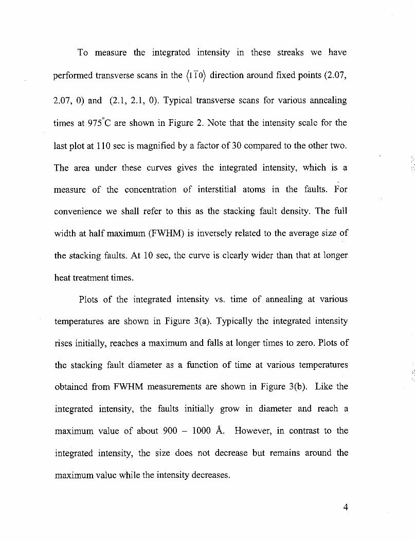
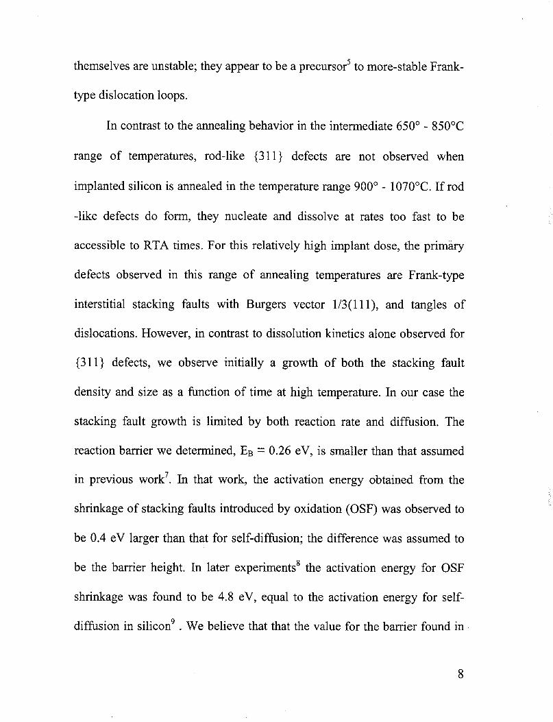
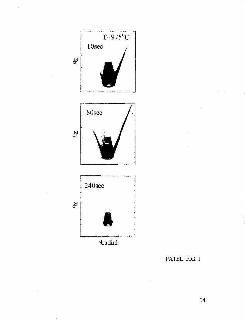
streaks. Maps of scattering in the qradial - q, plane at three values of
annealing time at 975’C are shown in Figure 1. The intensity map shows the
scattering around the (220) Bragg peak. The streaks of scattered intensity are --
accurately perpendicular’ to (111) and (1 1 1) crystal planes. It is known from
TEM studies2 that these faults are extrinsic in nature, each consisting of a
circular loop of an extra plane of atoms surrounded by a Frank-type partial
dislocation loop with l/3 ( 1 1 1 } Burgers vector.
3
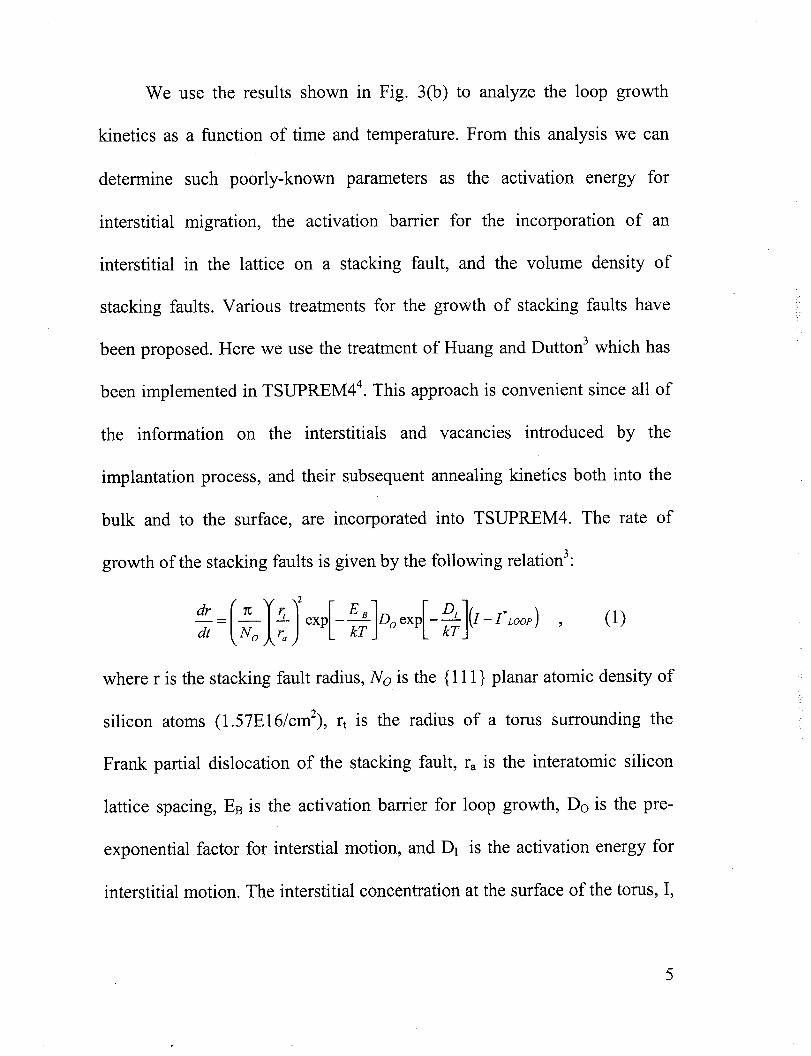
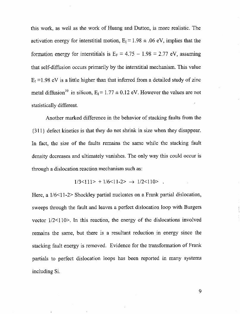
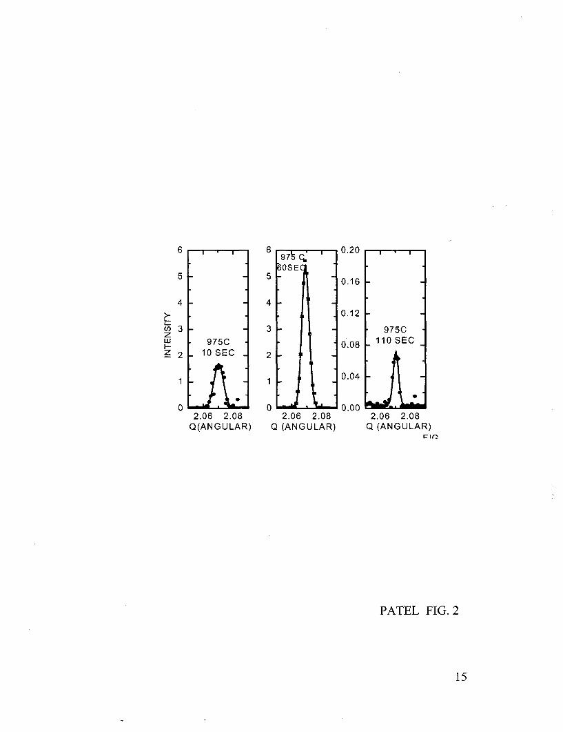
To measure the integrated intensity in these streaks we have
performed transverse scans in the (1 i0) direction around fixed points (2.07,
2.07, 0) and (2.1, 2.1, 0). Typical transverse scans for various annealing
times at 975’C are shown in Figure 2. Note that the intensity scale for the
last plot at 110 set is magnified by a factor of 30 compared to the other two.
The area under these curves gives the integrated intensity, which is a
measure of the concentration of interstitial atoms in the faults. For
convenience we shall refer to this as the stacking fault density. The full
width at half maximum (FWHM) is inversely related to the average size of
the stacking faults. At 10 set, the curve is clearly wider than that at longer
heat treatment times.
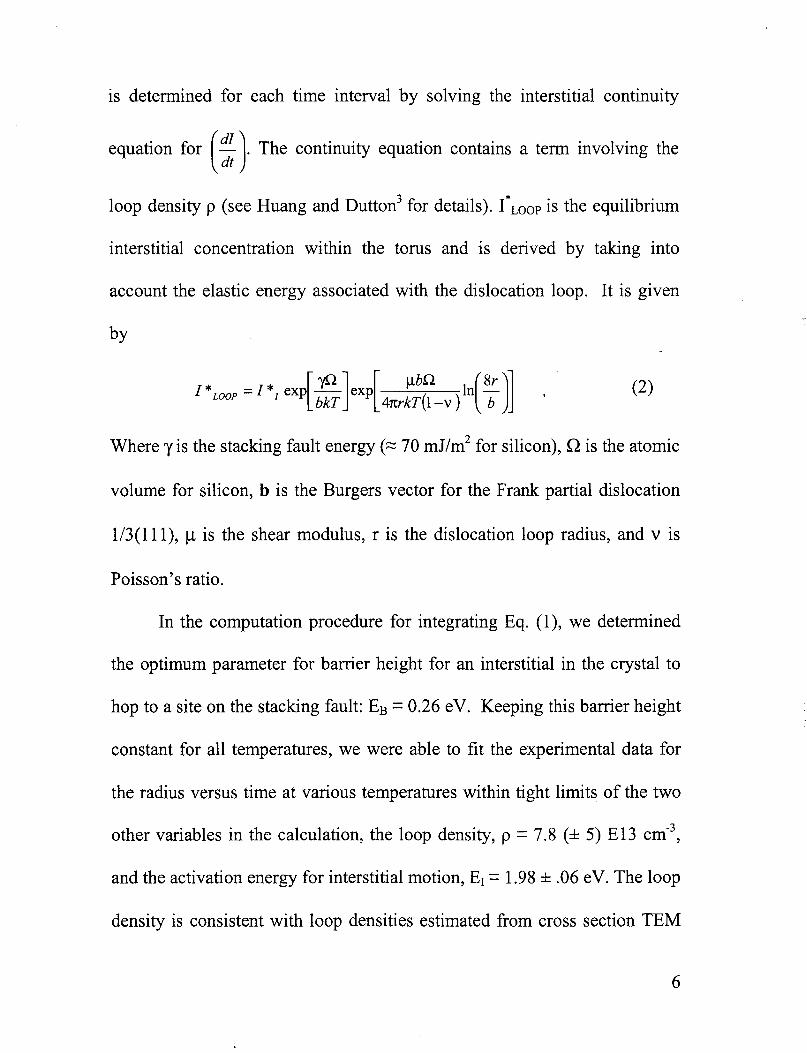
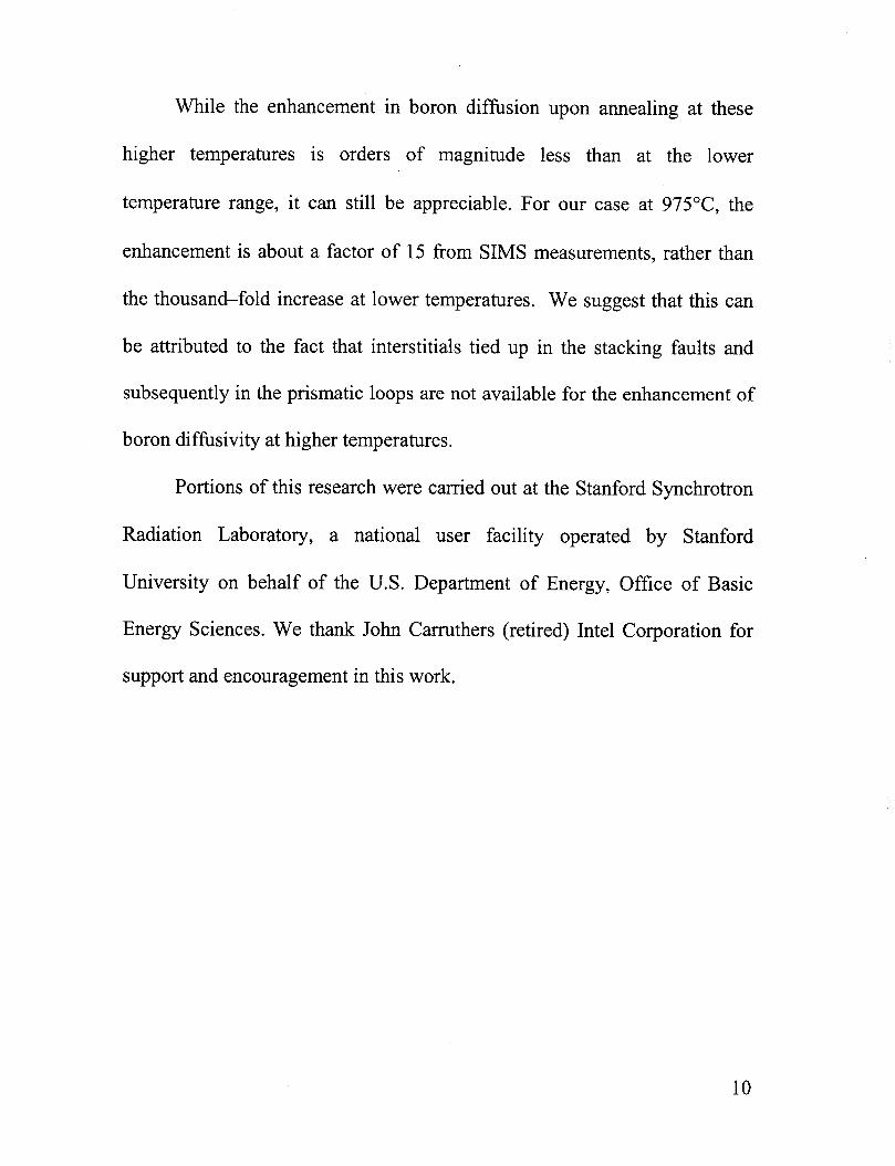
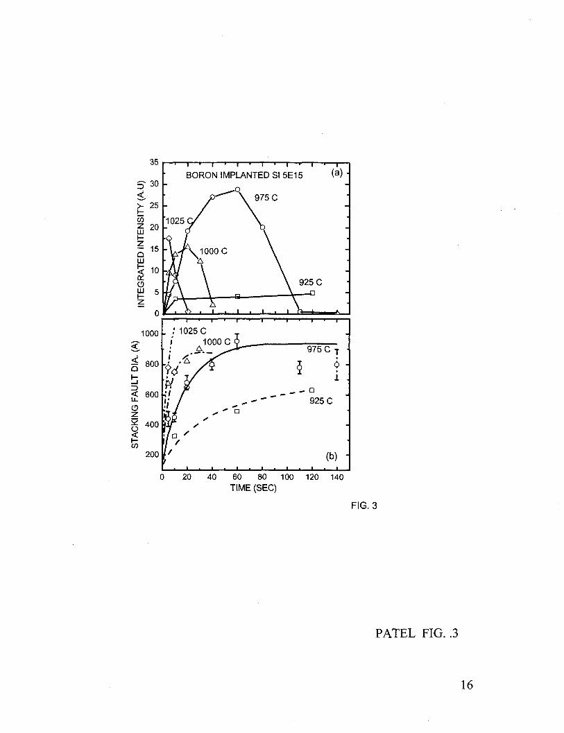
Plots of the integrated intensity vs. time of annealing at various
temperatures are shown in Figure 3(a). Typically the integrated intensity
rises initially, reaches a maximum and falls at longer times to zero. Plots of
the stacking fault diameter as a function of time at various temperatures
obtained from FWHM measurements are shown in Figure 3(b). Like the
integrated intensity, the faults initially grow in diameter and reach a
maximum value of about 900 - 1000 A. However, in contrast to the
integrated intensity, the size does not decrease but remains around the
maximum value while the intensity decreases.
4
We use the results shown in Fig. 3(b) to analyze the loop growth
kinetics as a function of time and temperature. From this analysis we can
determine such poorly-known parameters as the activation energy for
interstitial migration, the activation barrier for the incorporation of an
interstitial in the lattice on a stacking fault, and the volume density of
stacking faults. Various treatments for the growth of stacking faults have
been proposed. Here we use the treatment of Huang and Dutton3 which has
been implemented in TSUPREM44. This approach is convenient since all of
the information on the interstitials and vacancies introduced by the
implantation process, and their subsequent annealing kinetics both into the
bulk and to the surface, are incorporated into TSUPREM4. The rate of
growth of the stacking faults is given by the following relation3:
where r is the stacking fault radius, No is the ( 1 1 1 } planar atomic density of
silicon atoms (1.57El 6/cm2), r, is the radius of a torus surrounding the
Frank partial dislocation of the stacking fault, ra is the interatomic silicon
lattice spacing, EB is the activation barrier for loop growth, Do is the pre-
exponential factor for interstial motion, and Di is the activation energy for
interstitial motion. The interstitial concentration at the surface of the torus, I,
5
is determined for each time interval by solving the interstitial continuity
The continuity equation contains a term involving the
loop density p (see Huang and Dutton3 for details). I*Loop is the equilibrium
interstitial concentration within the torus and is derived by taking into
account the elastic energy associated with the dislocation loop. It is given
bY
I* = I *I exP IQ Clbfi - LOOP bkT 1 [ exp 4mkT(l -v ) ’
(2)
Where y is the stacking fault energy (= 70 mJ/m2 for silicon), LR is the atomic
volume for silicon, b is the Burgers vector for the Frank partial dislocation
l/3(1 1 1), lo is the shear modulus, r is the dislocation loop radius, and v is
Poisson’s ratio.
In the computation procedure for integrating Eq. (l), we determined
the optimum parameter for barrier height for an interstitial in the crystal to
hop to a site on the stacking fault: En = 0.26 eV. Keeping this barrier height
constant for all temperatures, we were able to fit the experimental data for
the radius versus time at various temperatures within tight limits of the two
other variables in the calculation, the loop density, p = 7.8 (f 5) El3 cma3,
and the activation energy for interstitial motion, Er = 1.98 f .06 eV. The loop
density is consistent with loop densities estimated from cross section TEM
6
observations. In Fig. 3(b) the fits are shown as lines; the points show
experimental data. Typical error bars for the 975” C data are also shown. For
the highest temperature (1025”C), the growth phase of the loops was too fast
to be experimentally accessible and we have arbitrarily fitted the growth
kinetics to the radius measured at the shortest time. Even in this extreme
case the calculation parameters are consistent with the other three
temperatures.
To put these relatively high temperature observations into context
with defect structures observed at lower temperatures, we note that when
implanted silicon is annealed in the temperature range 650” - 850°C the
initial extended defects formed are mainly rod-like5 along <l lO> with a
(3 1 l} habit plane. The (3 111 defects have been identified as an extra plane
of self-interstitial atoms, with aspect ratios of length to width typically about
10. Upon annealing, the larger defects grow at the expense of the smaller
ones. Their kinetics have been ascribed to an Ostwald ripening process. The
net concentration of interstitials in the defects never increases, but always
decreases with time of anneal. The interstial atoms released during annealing
contribute to transient enhanced difmsion (TED) during the annealing
process. Increases in the diffusion coefficient a thousand fold over the bulk
silicon value have been reported! However, the large (3 111 defects
7
themselves are unstable; they appear to be a precursor5 to more-stable Frank-
type dislocation loops.
In contrast to the annealing behavior in the intermediate 650” - 850°C
range of temperatures, rod-like (3 111 defects are not observed when
implanted silicon is annealed in the temperature range 900” - 1070°C. If rod
-like defects do form, they nucleate and dissolve at rates too fast to be
accessible to RTA times. For this relatively high implant dose, the primary
defects observed in this range of annealing temperatures are Frank-type
interstitial stacking faults with Burgers vector l/3(1 1 l), and tangles of
dislocations. However, in contrast to dissolution kinetics alone observed for
(31 l} defects, we observe initially a growth of both the stacking fault
density and size as a function of time at high temperature. In our case the
stacking fault growth is limited by both reaction rate and diffusion. The
reaction barrier we determined, En = 0.26 eV, is smaller than that assumed
in previous work7. In that work, the activation energy obtained from the
shrinkage of stacking faults introduced by oxidation (OSF) was observed to
be 0.4 eV larger than that for self-diffusion; the difference was assumed to
be the barrier height. In later experiments’ the activation energy for OSF
shrinkage was found to be 4.8 eV, equal to the activation energy for self-
diffusion in silicon’ . We believe that that the value for the barrier found in
8
this work, as well as the work of Huang and Dutton, is more realistic. The
activation energy for interstitial motion, Ei = 1.98 f .06 eV, implies that the
formation energy for interstitials is Er = 4.75 - 1.98 = 2.77 eV, assuming
that self-diffusion occurs primarily by the interstitial mechanism. This value
Ei x1.98 eV is a little higher than that inferred from a detailed study of zinc
metal diffusion” in silicon, Ei = 1.77 f 0.12 eV. However the values are not
statistically different.
Another marked difference in the behavior of stacking faults from the
(3 11) defect kinetics is that they do not shrink in size when they disappear.
In fact, the size of the faults remains the same while the stacking fault
density decreases and ultimately vanishes. The only way this could occur is
through a dislocation reaction mechanism such as:
1/3<111> + 1/6<1 l-2> + 1/2x110> .
Here, a 1/6<1 l-2> Shockley partial nucleates on a Frank partial dislocation,
sweeps through the fault and leaves a perfect dislocation loop with Burgers
vector 1/2<110>. In this reaction, the energy of the dislocations involved
remains the same, but there is a resultant reduction in energy since the
stacking fault energy is removed. Evidence for the transformation of Frank
partials to perfect dislocation loops has been reported in many systems
including Si.
While the enhancement in boron diffusion upon annealing at these
higher temperatures is orders of magnitude less than at the lower
temperature range, it can still be appreciable. For our case at 975”C, the
enhancement is about a factor of 15 from SIMS measurements, rather than
the thousand-fold increase at lower temperatures. We suggest that this can
be attributed to the fact that interstitials tied up in the stacking faults and
subsequently in the prismatic loops are not available for the enhancement of
boron diffusivity at higher temperatures.
Portions of this research were carried out at the Stanford Synchrotron
Radiation Laboratory, a national user facility operated by Stanford
University on behalf of the U.S. Department of Energy, Office of Basic
Energy Sciences. We thank John Carruthers (retired) Intel Corporation for
support and encouragement in this work.
10
REFERENCES
1. U. Beck, T. H. Metzger, J. Peisl, and J.R.Patel, Appl. Phys. Lett. 76,
2698 (2000) see also P. Erhart, H. Trinkaus and B.C. Larson, Phys.
Rev. B 25,834 (1982)
2. Bonafos, M. Omri, B. De Mauduit, G. BenAssayag, A. Claverie, D
Alquier, A. Martinez, and D. Mathiot, J. Appl. Phys. 82,2855 (1997)
3. R. Y. S. Huang and R. W. Dutton, J. Appl. Phys. 74,582 1 (1993) see
also S. T. Dunham, Appl. Phys. Lett. 63,484 (1993)
4. TSUPREM4 is a commercial version of the Stanford University
program SUPREM originally written at Stanford University by M. E.
Law, C. S. Rafferty, and R.W. Dutton.
5. D. J. Eaglesham, P. A. Stolk, H.-J. Gossmann, T. E. Haynes, and J. M.
Poate, Nucl. Instr. and Meth. in Phys. Research B, 106, 191 (1995)
6. A. E. Michel, W. Rausch, P. A. Ronsheim, and R. H. Kastl , Appl.
Phys. Lett. 50,416 (1987).
7. S. M. Hu in “Defects in Semiconductors” J. Narayan and T. Y. Tan,
Editors (North-Holland, Amsterdam, 1981) pp. 333 - 354.
8. A. Miin - Ron Lin, R. W. Dutton, D. A. Antoniadis, and W. A. Tiller,
J. Electrochem. So& 128, 1121 (198 1)
11
9. H.Bracht, E. E. Haller, and R. Clark-Phelps, Phys. Rev. Lett. 81,393
(1998)
10. H. Bracht, N. A. Stolwijk, and H. Mehrer, Phys. Rev. B, 16542
(1995)
12
FIGURE CAPTIONS
Figure 1. Diffuse scattering intensity in the q, - q, plane for silicon
implanted with a boron dose of 5E15 cms2 at 32 keV, and RTA annealed at
975’ C for the times shown. Note the growth and decay of the rod-like
streaks.
Figure 2. Angular scans through the streaks at (2.07, 2.07, 0) showing the
initial increase and the final decrease of intensity with time of heating at
975’ C. Note that the scale for the 110 set curve has been magnified by a
factor of 30.
Figure 3. (a): Integrated intensity of the streak scattering versus time of
anneal at the temperatures shown. (b): Stacking fault diameter derived from
the width of the streak. Note that while the integrated intensity grows,
reaches a maximum and subsequently decreases at long times of anneal, the
stacking fault diameter grows and stays at it’s maximum value even as the
intensity falls to zero.
13
240sec i
: -
qradial
PATEL FIG. 1
14
1
0
I ’ I
- 975c - _ IOSEC _
2.06 2.08 Q(ANGULAR)
6 -975 G
I
Q (ANGULAR) 2.06 2.08
0.20
0.16
0.12
0.08
0.04
0.00
I ’ I
- 975c - _ IIOSEC
Q (ANGULAR) CIC
2.06 2.08
PATEL FIG. 2
15
I , . , . , . , . , . , , ,
B O R O N IM P L A N T E D S I 5 E 1 5
2 2 8 0 0
5 z 6 0 0
9 7 5 c T
P 4 i
- a c- C-
9 2 5 c
(b )
0 2 0 4 0 6 0 8 0 1 0 0 1 2 0 1 4 0 TIME ( S E C )
FIG . 3
P A T E L F IG . .3
1 6