x-ray absorption studies of atomic environments in
TRANSCRIPT

X-ray Absorption studies ofatomic environments in
semiconductor nanostructures
Federico Boscherini
INFM and Department of PhysicsUniversity of Bologna, Italy
University of Bologna INFM

• Introduction– Why XAS for nanostructures– How XAS for nanostructures
• Interdiffusion in quantum dots and islands• Relation between local and long-range
elasticity in an “ideal” alloy: (InGa)As• Growth of nitride epilayers: a local view
University of Bologna INFM

Atomic structure in nanostructures
• As a result of reduceddimensions:– atomic intermixing
• in the “core”• at the interfaces
– variations in bond lengths
University of Bologna INFM
Sn cluster in SiO2 MDM-INFM
XAS to study nanostructures• XAS is a local, short range, effect
– same formalism applies to molecule, cluster orcrystalline solid
– insenstive to variations of morphology– sensitive to low thicknesses, high dilutions
• Excellent probe of variations in localenvironment upon reduction of dimensionsand/or dimensionality
University of Bologna INFM

Evolution of X-ray Absorption Spectroscopy• X-ray Absorption
Spectroscopy has greatlybenefited from– third generation SR sources
• high brilliance, extended energyrange, stability, reliability
– full theoretical understandingand reliable analysis programs
• XAS a reliable tool σ = σ 0
3 Sin2δ l =10 Im{T 1 −TG( )−1}1m ,1m
0,0
m∑
University of Bologna INFM
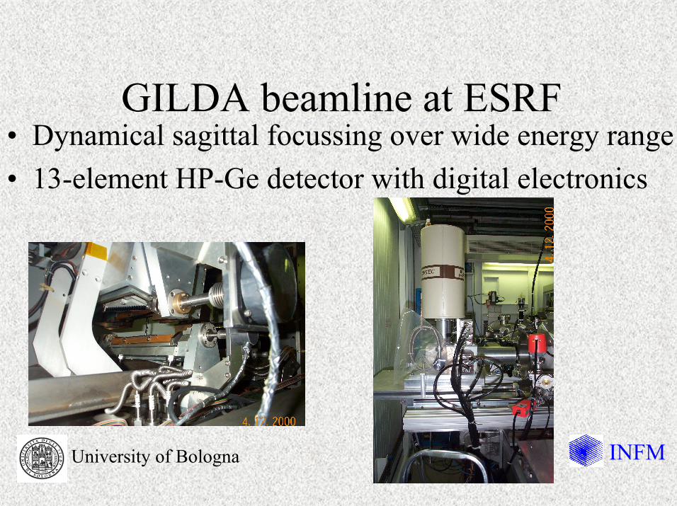
GILDA beamline at ESRF• Dynamical sagittal focussing over wide energy range• 13-element HP-Ge detector with digital electronics
University of Bologna INFM

GILDA experimental chamber• Transmission /
fluorescence• LNT - 150 °C
– reduce thermal damping• Rotatable holder
– polarization studies• Vibrating holder
– “smooth” Bragg peakeffects in single crystalepilayers
University of Bologna INFM

Atomic intermixing inGe/Si and InAs/GaAs quantum dots
University of Bologna INFM

Quantum dots
– F. Boscherini, G. Capellini, L. DiGaspare, F. Rosei, N. Motta,and S. Mobilio, Appl. Phys. Lett. 76, 682 (2000)
• Stranski-Krastanov growth leads to narrow sizedistribution of dots
• Need for understanding of local bonding
University of Bologna INFM

Energetics of island formation• Competing energies:
– strain– surface– dislocations
Wetting layer WL+Strained island WL+Relaxed island
"Coverage"
WL+2D platelet
• Contributions from:- wetting layer- islands
University of Bologna INFM

Preparation of Ge dots• Ge/Si(001) by CVD at University of Roma Tre, 600 °C
– Ex-situ AFM used to characterize degree of relaxation
• Ge/Si(111) by MBE at Tor Verg., 450 - 550 °C– In-situ STM/AFM
University of Bologna INFM

Ge/Si(001): AFM probes relaxation• Analysis of aspect ratio
provides measurementof relative amount ofrelaxed islands
• Ge/Si(001): Full rangeof relaxation examined
0
20
40
60
80
100
0 5 10 15 20 25 30 35 40
Rel
axed
vol
ume
(%)
equivalent thickness (nm)
Ge/Si(001)
(1 ML = 0.135 nm, WL = 3 ML)
University of Bologna INFM

Ge/Si(001): Ge K-edge XAFS
University of Bologna INFM
0
1
2
3
4
2 4 6 8 10 12 14 16k (Å-1)
k χ (
k) (Å
-1)
Ge:Si
(111)1 nm(001)
7.8 nm
(001)38 nm
Ge
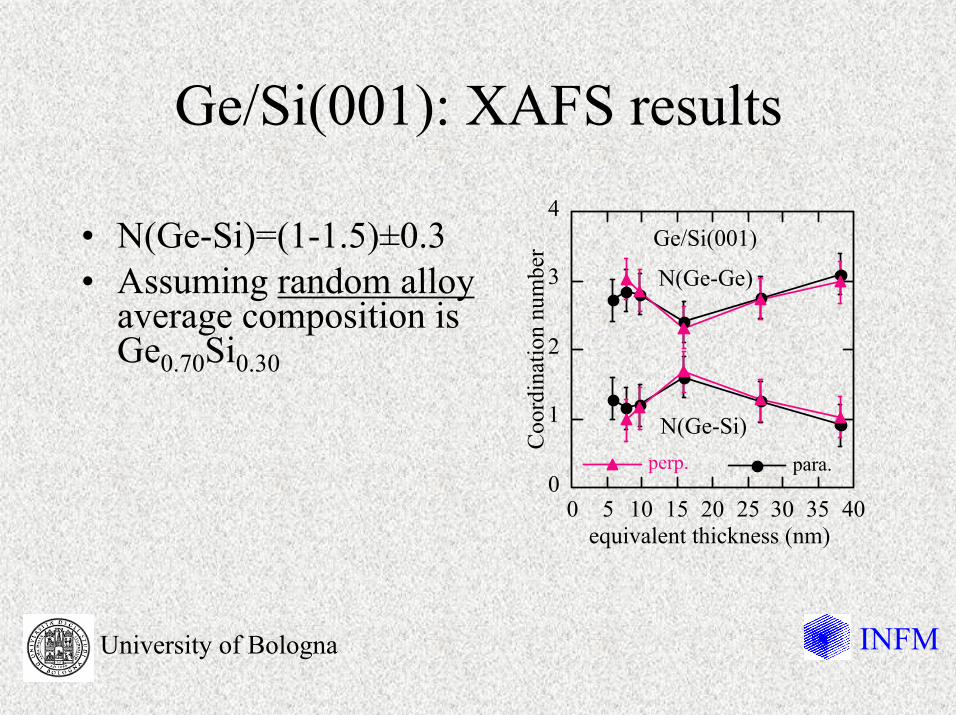
Ge/Si(001): XAFS results
• N(Ge-Si)=(1-1.5)±0.3• Assuming random alloy
average composition isGe0.70Si0.30
0
1
2
3
4
0 5 10 15 20 25 30 35 40
para.perp.
equivalent thickness (nm)C
oord
inat
ion
num
ber
N(Ge-Ge)
N(Ge-Si)
Ge/Si(001)
University of Bologna INFM

Ge/Si(111): XAFS
0
2
4
6
8
10
12
0 1 2 3 4 5 6
Mag
. Fou
. Tra
nsf.
[ k2 χ
(k)]
(Å
-3)
R (Å)
Ge in Si
Ge bulk
fed 5: 12.5 Å, 530 C
s1: 220 Å, 530 C
fed 3: 15 Å, 530 C
fed 11: 60 Å, 450 C
University of Bologna INFM
0,8
0,9
1
2
1 10 100
450 deg C530 deg C
N (G
e - S
i)thickness (nm)

Ge/Si(111): STM• A trench develops around the islands
– Si from the substrate diffusing into the island
University of Bologna INFM

InAs/GaAs(001): In K-edge XAFS• ALMBE, 10 ×
(3 ML InAs + 15 nmGaAs)
• Interdiffusionevident in 2nd shellsignal– Contraction of
bond length• In concentration in
dots: 0.25 - 0.450 1 2 3 4 5 6
R (Å)
InAssample
Mag
. Fou
. Tra
nsf.
University of Bologna INFM
2 4 6 8 10 12 14 16
k χ (
k) (Å
-1)
k (Å-1)
InAs
sample
0.0-0.1
0.10.20.3
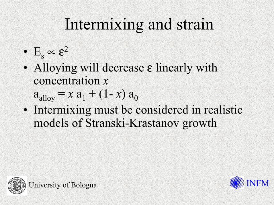
Intermixing and strain• Es ∝ ε2
• Alloying will decrease ε linearly withconcentration xaalloy = x a1 + (1- x) a0
• Intermixing must be considered in realisticmodels of Stranski-Krastanov growth
University of Bologna INFM
Local elasticity instrained epilayers
University of Bologna INFM

Local strain in 2Dsemiconductor epilayers
– Romanato et. al., Phys. Rev. B 57, 14619 (1998)– Tormen et. al. , J. Appl. Physics 86, 2533 (1999).– Tormen et. al. , Phys. Rev. B 63, 115326 (2001)
• What is the microscopic mechanism ofaccommodation of strain?
• What is the relation between long-range andshort range description of the elasticity ofsolids?
University of Bologna INFM
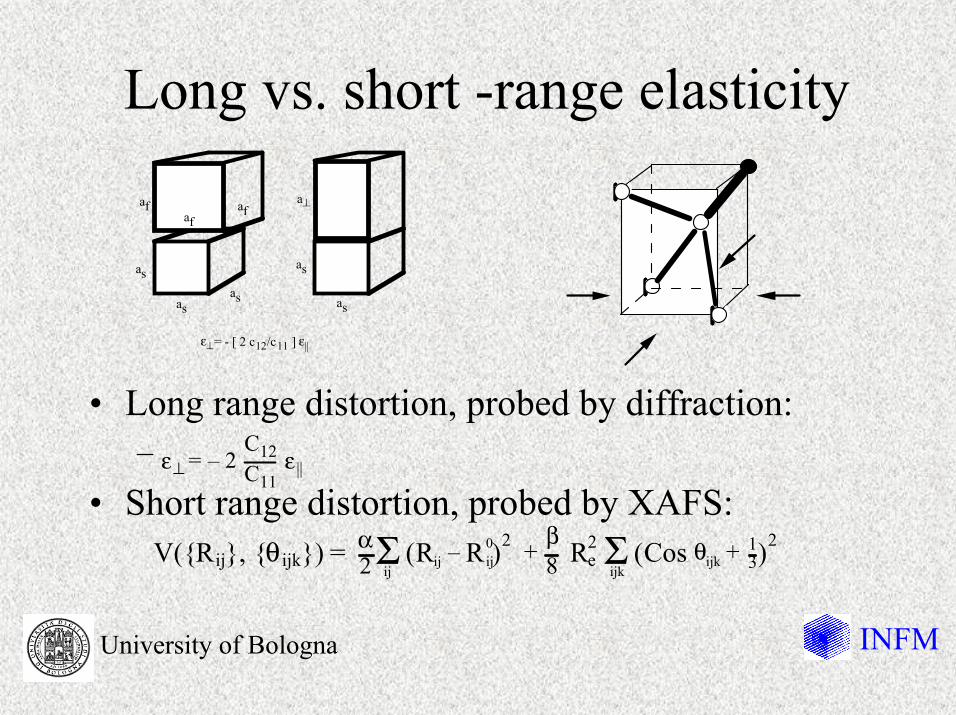
Long vs. short -range elasticity
• Long range distortion, probed by diffraction:–
• Short range distortion, probed by XAFS:
as
af
ε⊥= - [ 2 c12/c11 ] ε||
asas
af afa⊥
as
as
ε⊥ = – 2
C12C11
ε ||
University of Bologna INFM
V({Rij}, {θ ijk}) = α2 (Rij – Rij
0)2Σij
+β8 Re
2 (Cos θijk + 13)
2Σijk

Local distortions in unstrained alloys
V({Rij}, {θ ijk}) = α2 (Rij – Rij
0)2Σij
+β8 Re
2 (Cos θijk + 13)
2Σijk
• Local distortions in unstrained alloys are well understood • In semiconductors β/α = 0.1 - 0.2
• Bond lengths are “rigid”• Fundamental behavior can be obtained with
• no disorder in force constants• disorder in atomic radii
University of Bologna INFM
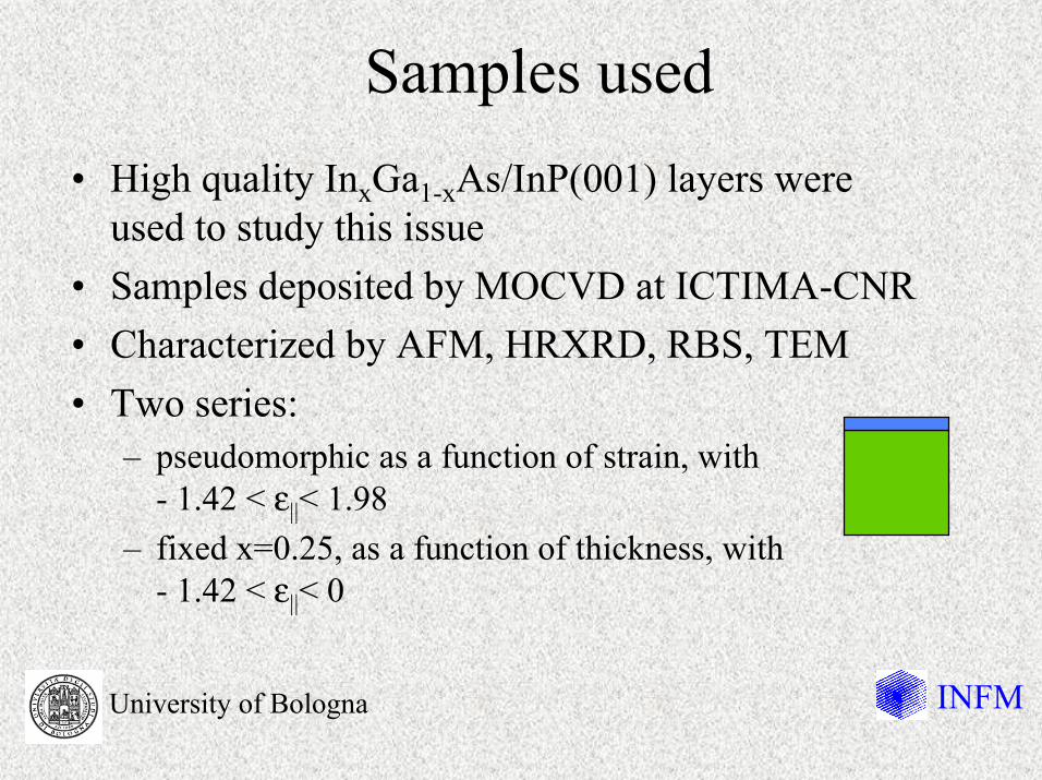
Samples used• High quality InxGa1-xAs/InP(001) layers were
used to study this issue• Samples deposited by MOCVD at ICTIMA-CNR• Characterized by AFM, HRXRD, RBS, TEM• Two series:
– pseudomorphic as a function of strain, with- 1.42 < ε||< 1.98
– fixed x=0.25, as a function of thickness, with- 1.42 < ε||< 0
University of Bologna INFM

Variation of bond lengths• A linear variation of bond lengths with strain is clearly
detected
2.44
2.46
2.48
2.50
2.52
2.54
0 0.2 0.4 0.6 0.8 1
R(G
a-A
s) (Å
)
xUniversity of Bologna INFM
-0,02
-0,01
0
0,01
0,02
-1,5 -1 -0,5 0 0,5 1 1,5 2δ
R (
Å)
strain (%)

Polarization dependence• Interatomic distances parallel and
perpendicular to growth plane canbe obtained
• In the plane wave approximationeach correlation contributes with aweight equal to
University of Bologna INFM
3 Cos2 ( ˆ E • ˆ r ij)
E
B krij
PARALLEL
PERPENDICULAR
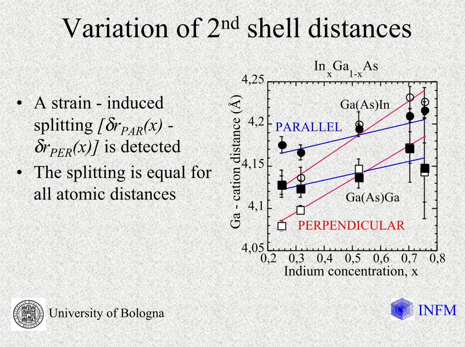
Variation of 2nd shell distances
• A strain - inducedsplitting [δrPAR(x) -δrPER(x)] is detected
• The splitting is equal forall atomic distances
University of Bologna INFM
4,05
4,1
4,15
4,2
4,25
0,2 0,3 0,4 0,5 0,6 0,7 0,8
InxGa
1-xAs
Indium concentration, x
Ga
- cat
ion
dist
ance
(Å)
Ga(As)In
Ga(As)Ga
PERPENDICULAR
PARALLEL
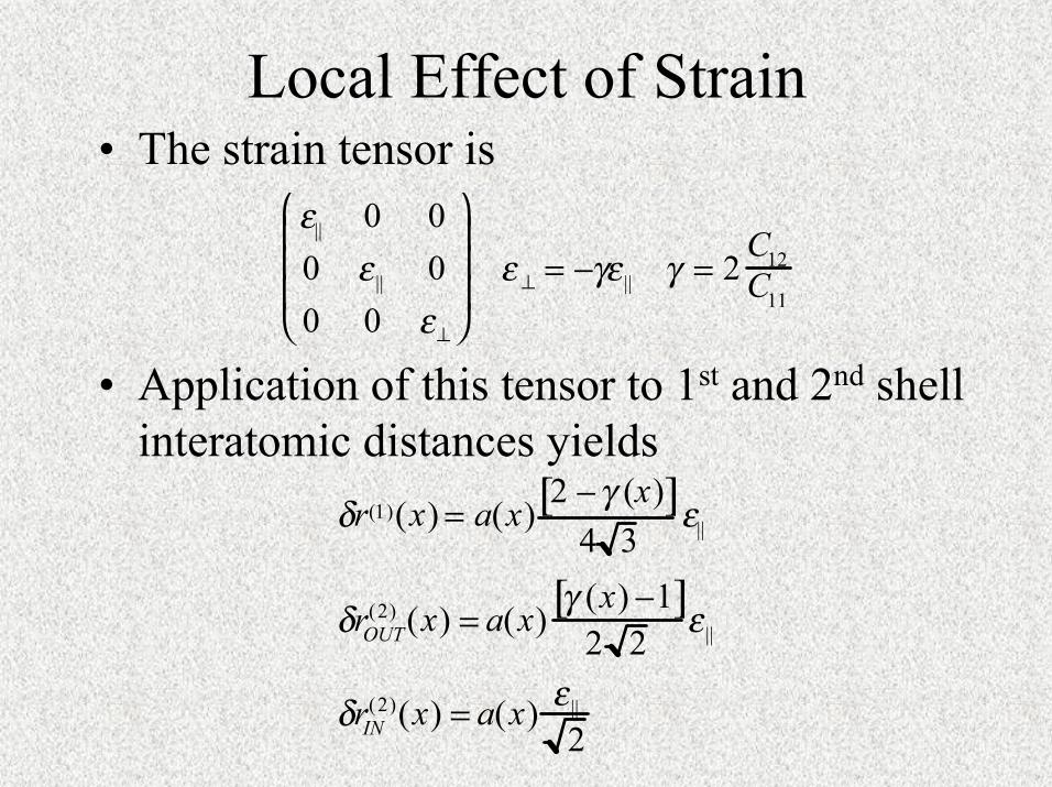
Local Effect of Strain• The strain tensor is
• Application of this tensor to 1st and 2nd shellinteratomic distances yields
ε|| 0 00 ε || 00 0 ε⊥
ε ⊥ = −γε || γ = 2C12C11
δr(1)(x) = a(x)2 −γ (x)[ ]
4 3ε||
δrOUT(2) (x) = a(x) γ (x) −1[ ]
2 2 ε ||
δrIN(2)(x) = a(x) ε ||
2
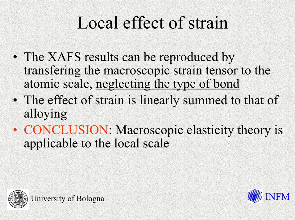
Local effect of strain
• The XAFS results can be reproduced bytransfering the macroscopic strain tensor to theatomic scale, neglecting the type of bond
• The effect of strain is linearly summed to that ofalloying
• CONCLUSION: Macroscopic elasticity theory isapplicable to the local scale
University of Bologna INFM

Growth of GaN epilayers:a local view

Growth of GaN on SiC and AlN– F. Boscherini, R. Lantier, A. Rizzi, F.
D’Acapito, and S. Mobilio, Appl. Phys. Lett.74, 3309 (1999) and submitted to PRB (2001)
• Nitrides are of great interest forrealization of blue-violetoptoelectronic devices
• Understanding of basic physics andgrowth mechanisms still matter ofactive research– No substrate with similar lattice
constant readily available
University of Bologna INFM

Issues addressed• Nitrides exhibit
– spontaneous polarization– strain-dependent piezoelectric polarization
• GaN/SiC abrupt is expected to be charged and unstable– intermixing is expected (Ga/Si or C/N mixed planes)
• Relation between morphology and local strain• Probe of elastic constants
• Samples grown at ISI, Forschungszentrum Jülich byMBE with rf plasma source N2
• XPS determination of band bending and band offsets
University of Bologna INFM

GaN/SiC: Ga XAFS
0.0
1.0
2.0
3.0
4.0
5.0
Mag
. FT
( χ (
k) k
2) (
Å-3
)R (Å)
0 1 2 3 4 1 2 3 4
PERPENDICULAR PARALLEL
University of Bologna INFM
Rbasal(2) = a
Roff − basal(2) = 1
3 a2 + 14 c2
Thickness: 0.7 - 150 nmR(2)(basal)
R(2)(off-basal)
PERP
END
ICU
LAR
PARALLEL
a
c

GaN/SiC• No change in 2nd shell distances, no
asymmetry between parallel andperpendicular directions– Relaxed growth (no piezoelectric polarization)
• No extensive intediffusion– High quality growth
• No Ga-Si mixed interface plane (C/N mixedplane cannot be excluded)
University of Bologna INFM

GaN/SiC: Impact• These results provide basis for:
– interpretation of XPS data– discussion and input to ab-initio electronic structure
calculations• Band-bending observed in XPS compatible with
relaxed growth• Valence band discontinuity of 0.8 ± 0.1 eV must
be attributed to relaxed interface• Note that all ab-initio calculations assume
pseudomorphic growth
University of Bologna INFM

GaN/AlN: dependence of morphologyon growth temperature
• “Smoother” epilayers for lower growth temperature
University of Bologna INFM
7 nm620 º C
7 nm790 °C
500 nm

GaN/AlN: Polarizationdependent Ga XANES
• Fingerprint ofwurtzite structure– 6 nm layers are
hexagonal• Reproduced by full
multiple scatteringcalculations
University of Bologna INFM
10360 10380 10400 10420 10440E (eV)
Abs
orpt
ion
coef
ficie
nt
PAR
PER
Simulation
Experiment
Simulation
Experiment
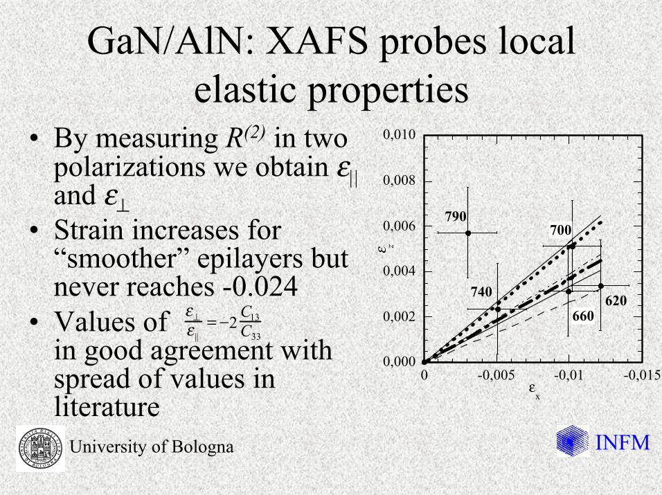
GaN/AlN: XAFS probes localelastic properties
• By measuring R(2) in twopolarizations we obtain ε||and ε⊥
• Strain increases for“smoother” epilayers butnever reaches -0.024
• Values ofin good agreement withspread of values inliterature
University of Bologna INFM
0,000
0,002
0,004
0,006
0,008
0,010
-0,015-0,01-0,0050ε z
εx
620
790
740660
700
ε⊥ε ||
= −2C13C33
Thanks• Ge islands
– G. Capellini, S. Mobilio, INFM +Univ. Rome 3– N. Motta, F. Rosei, INFM +Univ. Roma 2
• InAs dots– M. Capizzi, INFM + Univ. Rome 1– P. Frigeri and S. Franchi, MASPEC-CNR
• Local elasticity– D. De Salvador, F. Romanato, M. Tormen, A. Drigo,
INFM + Univ. Padova• GaN epilayers
– A. Rizzi, Jülich and INFM + Univ. Modena– F. D’Acapito, INFM Grenoble– S. Mobilio, INFN and Univ. Rome 3
University of Bologna INFM

Symposium I of theSpring Meeting of the
European Materials Research Society“Synchrotron Radiation and
Materials Science”June 18th - 21st, 2002Strasbourg, FRANCE
abstract deadline January 14th, 2002