wp - design soc using fpga-based ip an... · pdf fileadvantages and disadvantages of...
TRANSCRIPT

Fax: +1 408 549 9948
San Jose, CA 95110, USA 1754 Technology Drive, Suite 6 20
White Paper
Design SoC using FPGA-based IP An FGPA-Based ESL Methodology
June 2005
S2C Inc.
Tel: +1 408 213 8818
www.s2cinc.com

1
Introduction SoC design methodology has greatly matured over the past decade and many obstacles have been solved by improved semiconductor technologies, better EDA tools, and established design services. Also thanks to the rapid development of silicon IP industry, designers today can buy most of the design blocks required in an SoC in the market. So, what is the next wave of challenges for SoC design in the coming decade when the actual design processes seems to be getting easier? Definitely, putting these IP blocks in an optimal way becomes a key issue, especially when designers need to consider system level issues such as performance, bandwidth and power. Moreover, as software content for an SoC continues to enlarge, the ability to co-design software and hardware early becomes a necessity. This whitepaper introduces an FPGA-based electronic system level (ESL) methodology that utilizes FPGA-based IP models to create early system prototypes at near real-time speed that allow early software and hardware co-design. Utilizing ESL design tools and methodologies, SoC engineers can perform several steps simultaneously, such as architectural design, hardware/software partitioning, design, and verification, therefore enabling an easier and quicker design flow process. Today, most ESL tools are software-based. Although they can run at fairly fast speeds for the purpose of architectural design, the models used may not accurately represent the actual physical implementation and require either (i) manual translation to HDL, for the purpose of synthesizing and retargeting to a hardware implementation, or (ii) acquisition of external IP blocks that more accurately represent the actual implementation. Software-based ESL models are also deemed too slow for operating system (OS) integration and application testing, and thus necessitate the use of FPGA prototypes to validate the system before tape-out. Today, many IP providers offer FPGA-based reference boards for evaluation. However, it is an extremely onerous undertaking for a system designer to have to select IP from different vendors and then integrate several reference boards to form an SoC prototype with its own design. This white paper will expound on the benefits of a FPGA-based ESL environment and describe S2C’s patented TAI IP technology. With this technology, IP along with test points, system I/O, signal and event labels, and transactions are compiled into plug-and-play TAI IP blocks. One significant advantage of this approach is that TAI IP blocks can be plugged together to create an FPGA prototype, bypassing the time consuming and error prone manual translation to RTL. Another important benefit is that once they are compiled into TAI IP, IP blocks are secure and cannot be reverse engineered. This design and verification methodology promises to solve the many of the ESL design and IP security issues plaguing the industry by exploiting the next generation FPGA-based ESL design platforms that evaluate and exchange FPGA-based IP in TAI IP format. The first topic of discussion will be the challenges present in traditional ASIC design flows, as well as the advantages and disadvantages of software-based ESL design methodology, followed by the mechanics of FPGA-based ESL with TAI IP technology and how they can be used as a complementary enhancement on top of software-based ESL designs.

2
ASIC Design Flow and Common Issues Encountered
SoC SWDevelopment
SoC SWDevelopment
Synthesis &Layout
Synthesis &Layout
Design Sign-OffDesign Sign-Off
Functional Verification
Timing and PhysicalVerification
Functional VerificationSoftware Verification
System Validation
DesignSpecification
DesignSpecification
Verification Design Flow IP Library Usage
SWIP Library
SWIP Library
SoftIP Library
SoftIP Library
SiliconIP LibrarySilicon
IP Library
SoC HW RTL Development
SoC HW RTL Development
FPGAPrototype
FPGAPrototype
SoC SWDevelopment
SoC SWDevelopment
Synthesis &Layout
Synthesis &Layout
Design Sign-OffDesign Sign-Off
Functional Verification
Timing and PhysicalVerification
Functional VerificationSoftware Verification
System Validation
DesignSpecification
DesignSpecification
Verification Design Flow IP Library Usage
SWIP Library
SWIP Library
SoftIP Library
SoftIP Library
SiliconIP LibrarySilicon
IP Library
SoC HW RTL Development
SoC HW RTL Development
FPGAPrototype
FPGAPrototype
Figure 1: Traditional ASIC Design Flow The above diagram illustrates an SoC design based on a traditional ASIC design flow. As design projects move from ASICs to SoCs, many new and intractable problems have arisen: Architectural verification Optimizing SoC architectures necessitates the exploration and analysis of multiple candidate HW/SW partitioning schemes and hardware architectures, each with their own performance and economic trade-offs. In this phase, the SoC designer is primarily concerned with developing and optimizing system behavior and architecture. However, RTL’s pin-accurate connectivity and nanosecond-accurate timing detail obscure the system-wide view, thus slowing design speed considerably. Using this low productivity approach, designers occasionally settle for “whatever works” rather than “what works best” – and risk the launch of an uncompetitive product. A survey of leading SoC companies performed by International Business Strategies (IBS) forecasts that the time and effort required for SoC architectural development will soon exceed that of the physical design component, signifying that this productivity problem promises to become even worse. Functional verification Functional verification of RTL begins with the designer’s comprehensive interpretation of system-level behavior in terms of a profusion of intra-block circuit states and nanosecond-accurate transitions, together with their associated bit-accurate bus behaviors. It then requires the definition of a large number of detailed scenarios that exercise these behaviors along with the creation of multitudinous stimuli/expected responses for these
3
scenarios, followed by simulations that typically run at one-millionth of real chip speed. ASIC emulators or FPGA prototypes are often used to speed up the slow simulation speed. Software verification Embedded software, housing more than 50% of SoC functionality, is becoming the pacing item in SoC design. From the traditional design flow perspective, prior software development using “stubs” for peripherals can no longer adequately represent modern, multiprocessor, multibus architectures. Without an early virtual prototype, the software is developed in total isolation from the hardware, creating significant integration risk. The integration of software and system hardware at the tail-end of the design cycle can often lead to serious integration problems and makes time-to-market unpredictable. The use of FPGA prototypes to implement earlier integration represents only a moderate improvement to the schedule since prototypes still fail to arrive in time for software development. At this stage, even minor RTL design changes spurred by integration-related issues are time-consuming, directly delaying product time-to-market. System validation Building functional prototypes using FPGAs is today’s mainstream technique to fully validate SoCs in systems prior to tapeout. Not validating the designs in real or pseudo-real system environments creates a tremendous risk that the chips may not work in the target application after coming back from fabrication. However, in traditional ASIC design flow, designers can only start building FPGA prototypes after the majority of hardware developments are ready. In addition, system validation requires key software components to be ready, though completion of software development milestones also hinges on the time schedule of the FPGA prototype. This therefore makes system validation through the traditional ASIC design flow extremely painful. SoC Design Flow Using Software-based ESL SoC designers can benefit much from examining software-based ESL design methodologies. The following is the current design flow process based on software-based ESL.

4
System Design
System Design
SoC SWDevelopment
SoC SWDevelopment
SoC HW RTL Development
SoC HW RTL Development
Synthesis &Layout
Synthesis &Layout
Design Sign-OffDesign Sign-Off
FPGAPrototype
FPGAPrototype
Architectural VerificationAlgorithm Verification
Functional Verification
Timing and PhysicalVerification
Software Verification
Functional VerificationSoftware Verification
System Validation
DesignSpecification
DesignSpecification
SW-based ESLEnvironment
Verification Design Flow IP Library Usage
BehaviorIP LibraryBehaviorIP Library
SWIP Library
SWIP Library
SoftIP Library
SoftIP Library
SiliconIP LibrarySilicon
IP Library
System Design
System Design
SoC SWDevelopment
SoC SWDevelopment
SoC HW RTL Development
SoC HW RTL Development
Synthesis &Layout
Synthesis &Layout
Design Sign-OffDesign Sign-Off
FPGAPrototype
FPGAPrototype
Architectural VerificationAlgorithm Verification
Functional Verification
Timing and PhysicalVerification
Software Verification
Functional VerificationSoftware Verification
System Validation
DesignSpecification
DesignSpecification
SW-based ESLEnvironment
Verification Design Flow IP Library Usage
BehaviorIP LibraryBehaviorIP Library
SWIP Library
SWIP Library
SoftIP Library
SoftIP Library
SiliconIP LibrarySilicon
IP Library
Figure 2: SoC Design Flow using Software-based ESL Architectural verification Software-based ESL design accelerates complex hardware architecture development and HW/SW partitioning by executing at a higher level of abstraction than RTL, using only those design attributes relevant to system design. This is the level at which “design intent” is most meaningfully captured – a level the SoC architect has a direct and clear view of system behavior. Using transaction level modeling (TLM), the architecture is designed and verified in terms of functionality as characterized by high level block input and output events, and interblock data transfers. System IP components and buses not only may be modified or replaced with greater ease than at the RTL level, but also simulated at speeds more than 1,000 times faster. As a result, designers can quickly optimize the design to achieve “what works best.” Functional verification ESL design helps the functional verification of SoC hardware by verifying behavior in terms of high-level block input and output events, as well as inter-block data transfers, at the transaction level. Generation of system level test benches at the behavior level dramatically simplifies verification effort and time. ESL simulations co-simulate with SoC HW RTL can execute at speeds over 100 times faster than those of pure RTL simulations. Nevertheless, for more complex designs, hardware-based acceleration such as Emulators and FPGA prototypes are often used to complete the time-consuming functional verification cycles with large amount of test cases and data. Software development A TLM prototype advances commencement of software development by several months. Hardware-dependent software, such as real-time operating systems, can be ported over to the model without needing to connect

5
individual pins. Some application software, which is hardware-independent, may be developed and ported using the TLM as a data flow model. Software-based ESL design can co-verify hardware architecture with hardware-dependent software more than 1,000 times faster than RTL can. Hardware-independent software such as application software can be co-verified even more rapidly using a timing- and protocol-independent simulation. System validation System validation is performed on FPGA prototypes in software-based ESL design flows. However, key components of software that are required to perform system validation can be developed in software-based environments, making the task of system validation simpler compared to the traditional ASIC flow. Although software-based ESL design solves several key issues of system-level design, some new issues arising from this methodological change and other system–level design issues still remain unaddressed. Difficulty converting ESL Models to HDL designs ESL models need to be converted to HDL designs for physical implementation. Today, there are SystemC and behavior compilers that can do the process semi-automatically, but most of these tools are not mature. The majority of the designers still rely on either manual translation to HDL or the acquisition of external IP that represents the ESL model. These conversion processes are in many cases time-consuming and error prone. Creating accurate ESL models can be a tedious task While ESL models for some IP blocks can be created easily, the creation of models for other IP blocks can be a tedious task. In general, it is inherently much more difficult to behaviorally model non-algorithm intensive IP blocks. Modeling accuracy is also a concern for ESL design because the use of inaccurate ESL models can lead to incorrect architecture and algorithm designs, causing the actual chips to underperform or even fail to function in the target application. Ensuring that the newly created ESL models are indeed accurate representations of the physical IP is not a trivial task. Performance is still insufficient Software-based ESL model speeds are still too slow for serious OS integration and most application tests, therefore often still necessitating the use of FPGA prototypes to develop and verify software before tape-out. Difficulty in correlating between software-based ESL environment and hardware implementation Any bug-induced design changes implemented at the hardware level should be fed back to the software-based ESL environment to ensure that the architecture and algorithm are not affected. However, there is no straightforward correlation between today’s software-based ESL environment and the actual hardware implementation since there is a manual mapping step positioned between the software-based and hardware-based environments. As such, we posit that a high speed, high performance FPGA-based ESL design methodology provides a synergistic solution. FPGA-based ESL Design Flow and Benefits

6
The FPGA-based ESL design methodology is a system-level design flow where designers use plug-and-play FPGA-based IP models to create system configurations that are both accurate and high-performance. As figure three below illustrates, designers can perform architectural design, IP integration, software development, HW/SW co-verification, and FPGA prototyping all in the same FPGA-based ESL design platform.
System Design on FPGA Prototype
System Design on FPGA Prototype
SoC SWDevelopment
SoC SWDevelopment
SoC HW RTL Development
SoC HW RTL Development
Synthesis &Layout
Synthesis &Layout
Design Sign-OffDesign Sign-Off
Architectural VerificationAlgorithm VerificationFunctional VerificationSoftware Verification
System Validation
Timing and PhysicalVerification
System DesignBehavior
System DesignBehavior
FPGA-based ESL Environment
BehaviorIP LibraryBehaviorIP Library
SWIP Library
SWIP Library
SoftIP Library
SoftIP Library
SiliconIP LibrarySilicon
IP Library
TAIIP Library
TAIIP Library
Design Flow IP Library UsageVerification
DesignSpecification
DesignSpecification
Functional Verification
System Design on FPGA Prototype
System Design on FPGA Prototype
SoC SWDevelopment
SoC SWDevelopment
SoC HW RTL Development
SoC HW RTL Development
Synthesis &Layout
Synthesis &Layout
Design Sign-OffDesign Sign-Off
Architectural VerificationAlgorithm VerificationFunctional VerificationSoftware Verification
System Validation
Timing and PhysicalVerification
System DesignBehavior
System DesignBehavior
FPGA-based ESL Environment
BehaviorIP LibraryBehaviorIP Library
SWIP Library
SWIP Library
SoftIP Library
SoftIP Library
SiliconIP LibrarySilicon
IP Library
TAIIP Library
TAIIP Library
Design Flow IP Library UsageVerification
DesignSpecification
DesignSpecification
Functional Verification
Figure 3: SoC Design Flow using FPGA-based ESL Architectural verification FPGA-based ESL methodology further accelerates architectural verification by using plug-and-play FPGA-based IP models that are fast and accurate. FPGA-based IP models can be created easily from RTL IP — avoiding the potentially tedious process of compiling behavior ESL models to HDL. System designers can quickly configure the optimal architectures for their designs by using different FPGA-based IP models with different bus structures and run large amounts of test data near real time speeds on FPGA prototypes to ensure the correctness and proper performance of their system designs. Functional verification FPGA-based ESL ensures the highest throughput and highest coverage functional verification possible. Since system-level design, hardware development, and software development are performed on the common platform, functional verification is naturally performed at any time when any of these attributes change. In addition, FPGA-based ESL avoids the correlation difficulty between system-level design environments and actual hardware implementation present in software-based ESL. Software verification

7
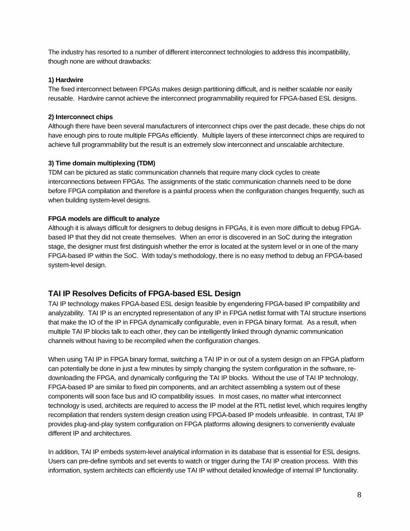
Software can be developed on a FPGA platform right from the beginning of the design cycle in an FPGA-based ESL flow. There is no need to port software from a software-based ESL model to FPGA prototypes, and software can be verified at real time or near real time speed right from the beginning. Any changes to the system and hardware can be re-run by software in a matter of hours. System validation An FPGA-based ESL design platform can be used for system validation, eliminating the need to build custom FPGA prototypes and saving one to three months of SoC project time. FPGA-based ESL provides the quickest path to an FPGA prototype by using pre-compiled FPGA-based IP libraries on re-configurable FPGA prototyping hardware. This not only greatly simplifies the compile process to FPGA but also allows third-party IP to be securely integrated in the FPGA prototypes for full system validation. Challenges of FPGA-based ESL Design SoC engineers have much to gain from adopting FPGA-based ESL design as a complementary solution; however, a number of issues must be taken into account. FPGA-based IP model incompatibility FPGA-based IP models are not readily compatible with each other. This stems from the fact that IP from different sources (vendor and internally developed IP), when delivered in FPGA-based format, cannot simply be easily integrated to form an SoC. This incompatibility in interconnecting the various IP blocks, as illustrated in the following diagram, is a frequently encountered challenge for designers:
?? ???? ??
FPGAbasedIP A
FPGAbasedIP A
FPGAbasedIP B
FPGAbasedIP B
FPGAbasedIP C
FPGAbasedIP C
FPGA based IP D
FPGA based IP D
FPGAbasedIP E
FPGAbasedIP E
?? Not fixed during architectural design ???? Not fixed during architectural design ??
FPGAbasedIP A
FPGAbasedIP A
FPGAbasedIP A
FPGAbasedIP A
FPGAbasedIP B
FPGAbasedIP B
FPGAbasedIP C
FPGAbasedIP C
FPGAbasedIP D
FPGAbasedIP D
FPGAbasedIP E
FPGAbasedIP E
Today’s Interconnect SolutionsHardwire
– Difficult to partition– Not reusable– Not scalable
Interconnect Chips– Limited pin– Difficult to scale
Time Domain Multiplexing– Slow– Requires recompilation– Cannot route fixed pin
components
Figure 4: Current Challenges in Interconnecting FPGA Models

8
The industry has resorted to a number of different interconnect technologies to address this incompatibility, though none are without drawbacks: 1) Hardwire The fixed interconnect between FPGAs makes design partitioning difficult, and is neither scalable nor easily reusable. Hardwire cannot achieve the interconnect programmability required for FPGA-based ESL designs. 2) Interconnect chips Although there have been several manufacturers of interconnect chips over the past decade, these chips do not have enough pins to route multiple FPGAs efficiently. Multiple layers of these interconnect chips are required to achieve full programmability but the result is an extremely slow interconnect and unscalable architecture. 3) Time domain multiplexing (TDM) TDM can be pictured as static communication channels that require many clock cycles to create interconnections between FPGAs. The assignments of the static communication channels need to be done before FPGA compilation and therefore is a painful process when the configuration changes frequently, such as when building system-level designs. FPGA models are difficult to analyze Although it is always difficult for designers to debug designs in FPGAs, it is even more difficult to debug FPGA-based IP that they did not create themselves. When an error is discovered in an SoC during the integration stage, the designer must first distinguish whether the error is located at the system level or in one of the many FPGA-based IP within the SoC. With today’s methodology, there is no easy method to debug an FPGA-based system-level design. TAI IP Resolves Deficits of FPGA-based ESL Design TAI IP technology makes FPGA-based ESL design feasible by engendering FPGA-based IP compatibility and analyzability. TAI IP is an encrypted representation of any IP in FPGA netlist format with TAI structure insertions that make the IO of the IP in FPGA dynamically configurable, even in FPGA binary format. As a result, when multiple TAI IP blocks talk to each other, they can be intelligently linked through dynamic communication channels without having to be recompiled when the configuration changes. When using TAI IP in FPGA binary format, switching a TAI IP in or out of a system design on an FPGA platform can potentially be done in just a few minutes by simply changing the system configuration in the software, re-downloading the FPGA, and dynamically configuring the TAI IP blocks. Without the use of TAI IP technology, FPGA-based IP are similar to fixed pin components, and an architect assembling a system out of these components will soon face bus and IO compatibility issues. In most cases, no matter what interconnect technology is used, architects are required to access the IP model at the RTL netlist level, which requires lengthy recompilation that renders system design creation using FPGA-based IP models unfeasible. In contrast, TAI IP provides plug-and-play system configuration on FPGA platforms allowing designers to conveniently evaluate different IP and architectures. In addition, TAI IP embeds system-level analytical information in its database that is essential for ESL designs. Users can pre-define symbols and set events to watch or trigger during the TAI IP creation process. With this information, system architects can efficiently use TAI IP without detailed knowledge of internal IP functionality.

9
Dynamic channelsDynamic channels
FPGAbasedIP A
FPGAbasedIP A
FPGAbasedIP B
FPGAbasedIP B
FPGAbasedIP C
FPGAbasedIP C
FPGA based IP D
FPGA based IP D
FPGAbasedIP E
FPGAbasedIP E
?? Not fixed during architectural design ???? Not fixed during architectural design ??
FPGAbasedIP A
FPGAbasedIP A
FPGAbasedIP A
FPGAbasedIP A
FPGAbasedIP B
FPGAbasedIP B
FPGAbasedIP C
FPGAbasedIP C
FPGAbasedIP D
FPGAbasedIP D
FPGAbasedIP E
FPGAbasedIP E
TAI TAI
TAI IP™ TechnologyPlug-and-play FPGA-based Model
– Supports FPGA binary format and avoids FPGA re-compile
Dynamic Communication Channels
– Fastest interconnect when hardwire is not feasible
– 100% routable and scalable System Level Debugging
– Embeds symbols and events in TAI IP
– Zoom in and out of debugging area on the fly
TAI TAI TAI TAI
Figure 5: FPGA-based IP Integration of TAI IP Technology
Complementary Solutions: Linking FPGA-based ESL with Software-based ESL TAI IP-enhanced FPGA-based ESL can be used not only independently but also combined with software-based ESL to enable architectural exploration and algorithm development. For instance, a designer may sometimes rely on SystemC models instead of FPGA-based IP models for a preliminary design at the beginning of the design process. In this case, the designer can place the SystemC models in WS or PC software-based tools and the remaining TAI IP in the FPGA-based ESL platform. They can then communicate at the transaction level through specific synthesizable bus functional models (BFM) using hardware speed. Algorithm design and verification is a strongpoint of software-based ESL tools, and they too can be linked with FPGA-based ESL platforms through BFMs. Another instance where linking FPGA- and software-based ESL would be beneficial is when prototyping speeds do not match the real targets. In Gigabit Ethernet applications, for example, an FPGA prototype will have a hard time running at the same speeds as those of the target, so the designer works around this limitation by modeling the target in a workstation or PC to form a virtual prototype environment. This technology provides various and efficient ways to prototype designs and meet diversiform requirements. The following chart illustrates how FPGA-based ESL can be linked with software-based ESL to form a virtual prototype.

10
SystemCWrappers
Test API
DUTDUT
HDL in FPGA-based ESL Environment
SystemC or Standard ESL in PC/WS
TestsTests
Device-specific BFMDevice-specific BFM
Abstraction/Modeling Layer
Traffic Gen
Simple SystemC Transaction API SCE-MI
Messaging, Logging
StandardProtocol Specific
PCPC
Control
Clk CntlOut Port
2 Port Xactor RAM
In Port
Figure 6: Linkage Structure between FPGA-based ESL and Software-based ESL Conclusion The majority of SoC projects today require both IP-based design using ESL methodology and FPGA prototypes for system integration, compliance testing, and manufacturing test development before chip fabrication proceeds. It is therefore apparent that the industry needs to have a methodology that employs FPGA-based IP libraries to engage in system-level design and verification – although challenges do exist in using FPGA-based IP models for system-level design, namely in the areas of system integration, analysis, and debugging. Applying FPGA-based ESL designs with a TAI IP-format library enables designers to perform system-level design while doing away with these limitations. This methodology combines the advantages of both the prototype’s speed and software-based ESL’s analytical functionality, which solves the problem of debugging and integrating FPGA prototypes. It also accelerates software-based ESL tool speeds to design, analyze, and verify the architecture. Finally, IP security is a major concern for system-level designs, and TAI IP may be distributed freely without concerns of reverse engineering. Using FPGA-based ESL, independently or in combination with software-based ESL tools, empowers designers with the means to resolve almost any difficulty they encounter in the stages of architectural design, verification, and prototyping.

11
About S2C Inc. Founded and headquartered in San Jose, California, S2C is the leading total solution provider in facilitating systems to chip innovations. S2C has three solutions for system-on-chip (SoC) development:
• Rapid SoC prototyping on Field Programmable Gate Array (FPGA) • Third-party silicon intellectual properties (IP) • SoC design, prototype and production services
S2C’s value proposition is our highly qualified engineering team and customer-focused sales force that understands our customers’ commercial needs in SoC development. S2C’s unique FPGA-based electronic system level (ESL) solution, using our patented TAI IP technology, enables designers who employ silicon IP to quickly assemble SoC prototypes on FPGA easily and securely, thereby enabling customers to start software development, typically the long pole item in development schedules, immediately. Combining rapid prototyping methodologies with a comprehensive portfolio of silicon IP and advanced design solutions, S2C can reduce the SoC design cycle by up to nine months. S2C currently has 3 direct offices located in Shanghai, Beijing and Shenzhen to meet the demand for accelerated SoC design activities in China. S2C is also the organizer of the annual SoCIP symposium in China, which brings SoC designers/professionals from the region and international silicon IP and SoC solution vendors together.

1
Introduction SoC design methodology has greatly matured over the past decade and many obstacles have been solved by improved semiconductor technologies, better EDA tools, and established design services. Also thanks to the rapid development of silicon IP industry, designers today can buy most of the design blocks required in an SoC in the market. So, what is the next wave of challenges for SoC design in the coming decade when the actual design processes seems to be getting easier? Definitely, putting these IP blocks in an optimal way becomes a key issue, especially when designers need to consider system level issues such as performance, bandwidth and power. Moreover, as software content for an SoC continues to enlarge, the ability to co-design software and hardware early becomes a necessity. This whitepaper introduces an FPGA-based electronic system level (ESL) methodology that utilizes FPGA-based IP models to create early system prototypes at near real-time speed that allow early software and hardware co-design. Utilizing ESL design tools and methodologies, SoC engineers can perform several steps simultaneously, such as architectural design, hardware/software partitioning, design, and verification, therefore enabling an easier and quicker design flow process. Today, most ESL tools are software-based. Although they can run at fairly fast speeds for the purpose of architectural design, the models used may not accurately represent the actual physical implementation and require either (i) manual translation to HDL, for the purpose of synthesizing and retargeting to a hardware implementation, or (ii) acquisition of external IP blocks that more accurately represent the actual implementation. Software-based ESL models are also deemed too slow for operating system (OS) integration and application testing, and thus necessitate the use of FPGA prototypes to validate the system before tape-out. Today, many IP providers offer FPGA-based reference boards for evaluation. However, it is an extremely onerous undertaking for a system designer to have to select IP from different vendors and then integrate several reference boards to form an SoC prototype with its own design. This white paper will expound on the benefits of a FPGA-based ESL environment and describe S2C’s patented TAI IP technology. With this technology, IP along with test points, system I/O, signal and event labels, and transactions are compiled into plug-and-play TAI IP blocks. One significant advantage of this approach is that TAI IP blocks can be plugged together to create an FPGA prototype, bypassing the time consuming and error prone manual translation to RTL. Another important benefit is that once they are compiled into TAI IP, IP blocks are secure and cannot be reverse engineered. This design and verification methodology promises to solve the many of the ESL design and IP security issues plaguing the industry by exploiting the next generation FPGA-based ESL design platforms that evaluate and exchange FPGA-based IP in TAI IP format. The first topic of discussion will be the challenges present in traditional ASIC design flows, as well as the advantages and disadvantages of software-based ESL design methodology, followed by the mechanics of FPGA-based ESL with TAI IP technology and how they can be used as a complementary enhancement on top of software-based ESL designs.

2
ASIC Design Flow and Common Issues Encountered
SoC SWDevelopment
SoC SWDevelopment
Synthesis &Layout
Synthesis &Layout
Design Sign-OffDesign Sign-Off
Functional Verification
Timing and PhysicalVerification
Functional VerificationSoftware Verification
System Validation
DesignSpecification
DesignSpecification
Verification Design Flow IP Library Usage
SWIP Library
SWIP Library
SoftIP Library
SoftIP Library
SiliconIP LibrarySilicon
IP Library
SoC HW RTL Development
SoC HW RTL Development
FPGAPrototype
FPGAPrototype
SoC SWDevelopment
SoC SWDevelopment
Synthesis &Layout
Synthesis &Layout
Design Sign-OffDesign Sign-Off
Functional Verification
Timing and PhysicalVerification
Functional VerificationSoftware Verification
System Validation
DesignSpecification
DesignSpecification
Verification Design Flow IP Library Usage
SWIP Library
SWIP Library
SoftIP Library
SoftIP Library
SiliconIP LibrarySilicon
IP Library
SoC HW RTL Development
SoC HW RTL Development
FPGAPrototype
FPGAPrototype
Figure 1: Traditional ASIC Design Flow The above diagram illustrates an SoC design based on a traditional ASIC design flow. As design projects move from ASICs to SoCs, many new and intractable problems have arisen: Architectural verification Optimizing SoC architectures necessitates the exploration and analysis of multiple candidate HW/SW partitioning schemes and hardware architectures, each with their own performance and economic trade-offs. In this phase, the SoC designer is primarily concerned with developing and optimizing system behavior and architecture. However, RTL’s pin-accurate connectivity and nanosecond-accurate timing detail obscure the system-wide view, thus slowing design speed considerably. Using this low productivity approach, designers occasionally settle for “whatever works” rather than “what works best” – and risk the launch of an uncompetitive product. A survey of leading SoC companies performed by International Business Strategies (IBS) forecasts that the time and effort required for SoC architectural development will soon exceed that of the physical design component, signifying that this productivity problem promises to become even worse. Functional verification Functional verification of RTL begins with the designer’s comprehensive interpretation of system-level behavior in terms of a profusion of intra-block circuit states and nanosecond-accurate transitions, together with their associated bit-accurate bus behaviors. It then requires the definition of a large number of detailed scenarios that exercise these behaviors along with the creation of multitudinous stimuli/expected responses for these

3
scenarios, followed by simulations that typically run at one-millionth of real chip speed. ASIC emulators or FPGA prototypes are often used to speed up the slow simulation speed. Software verification Embedded software, housing more than 50% of SoC functionality, is becoming the pacing item in SoC design. From the traditional design flow perspective, prior software development using “stubs” for peripherals can no longer adequately represent modern, multiprocessor, multibus architectures. Without an early virtual prototype, the software is developed in total isolation from the hardware, creating significant integration risk. The integration of software and system hardware at the tail-end of the design cycle can often lead to serious integration problems and makes time-to-market unpredictable. The use of FPGA prototypes to implement earlier integration represents only a moderate improvement to the schedule since prototypes still fail to arrive in time for software development. At this stage, even minor RTL design changes spurred by integration-related issues are time-consuming, directly delaying product time-to-market. System validation Building functional prototypes using FPGAs is today’s mainstream technique to fully validate SoCs in systems prior to tapeout. Not validating the designs in real or pseudo-real system environments creates a tremendous risk that the chips may not work in the target application after coming back from fabrication. However, in traditional ASIC design flow, designers can only start building FPGA prototypes after the majority of hardware developments are ready. In addition, system validation requires key software components to be ready, though completion of software development milestones also hinges on the time schedule of the FPGA prototype. This therefore makes system validation through the traditional ASIC design flow extremely painful. SoC Design Flow Using Software-based ESL SoC designers can benefit much from examining software-based ESL design methodologies. The following is the current design flow process based on software-based ESL.

4
System Design
System Design
SoC SWDevelopment
SoC SWDevelopment
SoC HW RTL Development
SoC HW RTL Development
Synthesis &Layout
Synthesis &Layout
Design Sign-OffDesign Sign-Off
FPGAPrototype
FPGAPrototype
Architectural VerificationAlgorithm Verification
Functional Verification
Timing and PhysicalVerification
Software Verification
Functional VerificationSoftware Verification
System Validation
DesignSpecification
DesignSpecification
SW-based ESLEnvironment
Verification Design Flow IP Library Usage
BehaviorIP LibraryBehaviorIP Library
SWIP Library
SWIP Library
SoftIP Library
SoftIP Library
SiliconIP LibrarySilicon
IP Library
System Design
System Design
SoC SWDevelopment
SoC SWDevelopment
SoC HW RTL Development
SoC HW RTL Development
Synthesis &Layout
Synthesis &Layout
Design Sign-OffDesign Sign-Off
FPGAPrototype
FPGAPrototype
Architectural VerificationAlgorithm Verification
Functional Verification
Timing and PhysicalVerification
Software Verification
Functional VerificationSoftware Verification
System Validation
DesignSpecification
DesignSpecification
SW-based ESLEnvironment
Verification Design Flow IP Library Usage
BehaviorIP LibraryBehaviorIP Library
SWIP Library
SWIP Library
SoftIP Library
SoftIP Library
SiliconIP LibrarySilicon
IP Library
Figure 2: SoC Design Flow using Software-based ESL Architectural verification Software-based ESL design accelerates complex hardware architecture development and HW/SW partitioning by executing at a higher level of abstraction than RTL, using only those design attributes relevant to system design. This is the level at which “design intent” is most meaningfully captured – a level the SoC architect has a direct and clear view of system behavior. Using transaction level modeling (TLM), the architecture is designed and verified in terms of functionality as characterized by high level block input and output events, and interblock data transfers. System IP components and buses not only may be modified or replaced with greater ease than at the RTL level, but also simulated at speeds more than 1,000 times faster. As a result, designers can quickly optimize the design to achieve “what works best.” Functional verification ESL design helps the functional verification of SoC hardware by verifying behavior in terms of high-level block input and output events, as well as inter-block data transfers, at the transaction level. Generation of system level test benches at the behavior level dramatically simplifies verification effort and time. ESL simulations co-simulate with SoC HW RTL can execute at speeds over 100 times faster than those of pure RTL simulations. Nevertheless, for more complex designs, hardware-based acceleration such as Emulators and FPGA prototypes are often used to complete the time-consuming functional verification cycles with large amount of test cases and data. Software development A TLM prototype advances commencement of software development by several months. Hardware-dependent software, such as real-time operating systems, can be ported over to the model without needing to connect

5
individual pins. Some application software, which is hardware-independent, may be developed and ported using the TLM as a data flow model. Software-based ESL design can co-verify hardware architecture with hardware-dependent software more than 1,000 times faster than RTL can. Hardware-independent software such as application software can be co-verified even more rapidly using a timing- and protocol-independent simulation. System validation System validation is performed on FPGA prototypes in software-based ESL design flows. However, key components of software that are required to perform system validation can be developed in software-based environments, making the task of system validation simpler compared to the traditional ASIC flow. Although software-based ESL design solves several key issues of system-level design, some new issues arising from this methodological change and other system–level design issues still remain unaddressed. Difficulty converting ESL Models to HDL designs ESL models need to be converted to HDL designs for physical implementation. Today, there are SystemC and behavior compilers that can do the process semi-automatically, but most of these tools are not mature. The majority of the designers still rely on either manual translation to HDL or the acquisition of external IP that represents the ESL model. These conversion processes are in many cases time-consuming and error prone. Creating accurate ESL models can be a tedious task While ESL models for some IP blocks can be created easily, the creation of models for other IP blocks can be a tedious task. In general, it is inherently much more difficult to behaviorally model non-algorithm intensive IP blocks. Modeling accuracy is also a concern for ESL design because the use of inaccurate ESL models can lead to incorrect architecture and algorithm designs, causing the actual chips to underperform or even fail to function in the target application. Ensuring that the newly created ESL models are indeed accurate representations of the physical IP is not a trivial task. Performance is still insufficient Software-based ESL model speeds are still too slow for serious OS integration and most application tests, therefore often still necessitating the use of FPGA prototypes to develop and verify software before tape-out. Difficulty in correlating between software-based ESL environment and hardware implementation Any bug-induced design changes implemented at the hardware level should be fed back to the software-based ESL environment to ensure that the architecture and algorithm are not affected. However, there is no straightforward correlation between today’s software-based ESL environment and the actual hardware implementation since there is a manual mapping step positioned between the software-based and hardware-based environments. As such, we posit that a high speed, high performance FPGA-based ESL design methodology provides a synergistic solution. FPGA-based ESL Design Flow and Benefits

6
The FPGA-based ESL design methodology is a system-level design flow where designers use plug-and-play FPGA-based IP models to create system configurations that are both accurate and high-performance. As figure three below illustrates, designers can perform architectural design, IP integration, software development, HW/SW co-verification, and FPGA prototyping all in the same FPGA-based ESL design platform.
System Design on FPGA Prototype
System Design on FPGA Prototype
SoC SWDevelopment
SoC SWDevelopment
SoC HW RTL Development
SoC HW RTL Development
Synthesis &Layout
Synthesis &Layout
Design Sign-OffDesign Sign-Off
Architectural VerificationAlgorithm VerificationFunctional VerificationSoftware Verification
System Validation
Timing and PhysicalVerification
System DesignBehavior
System DesignBehavior
FPGA-based ESL Environment
BehaviorIP LibraryBehaviorIP Library
SWIP Library
SWIP Library
SoftIP Library
SoftIP Library
SiliconIP LibrarySilicon
IP Library
TAIIP Library
TAIIP Library
Design Flow IP Library UsageVerification
DesignSpecification
DesignSpecification
Functional Verification
System Design on FPGA Prototype
System Design on FPGA Prototype
SoC SWDevelopment
SoC SWDevelopment
SoC HW RTL Development
SoC HW RTL Development
Synthesis &Layout
Synthesis &Layout
Design Sign-OffDesign Sign-Off
Architectural VerificationAlgorithm VerificationFunctional VerificationSoftware Verification
System Validation
Timing and PhysicalVerification
System DesignBehavior
System DesignBehavior
FPGA-based ESL Environment
BehaviorIP LibraryBehaviorIP Library
SWIP Library
SWIP Library
SoftIP Library
SoftIP Library
SiliconIP LibrarySilicon
IP Library
TAIIP Library
TAIIP Library
Design Flow IP Library UsageVerification
DesignSpecification
DesignSpecification
Functional Verification
Figure 3: SoC Design Flow using FPGA-based ESL Architectural verification FPGA-based ESL methodology further accelerates architectural verification by using plug-and-play FPGA-based IP models that are fast and accurate. FPGA-based IP models can be created easily from RTL IP — avoiding the potentially tedious process of compiling behavior ESL models to HDL. System designers can quickly configure the optimal architectures for their designs by using different FPGA-based IP models with different bus structures and run large amounts of test data near real time speeds on FPGA prototypes to ensure the correctness and proper performance of their system designs. Functional verification FPGA-based ESL ensures the highest throughput and highest coverage functional verification possible. Since system-level design, hardware development, and software development are performed on the common platform, functional verification is naturally performed at any time when any of these attributes change. In addition, FPGA-based ESL avoids the correlation difficulty between system-level design environments and actual hardware implementation present in software-based ESL. Software verification

7
Software can be developed on a FPGA platform right from the beginning of the design cycle in an FPGA-based ESL flow. There is no need to port software from a software-based ESL model to FPGA prototypes, and software can be verified at real time or near real time speed right from the beginning. Any changes to the system and hardware can be re-run by software in a matter of hours. System validation An FPGA-based ESL design platform can be used for system validation, eliminating the need to build custom FPGA prototypes and saving one to three months of SoC project time. FPGA-based ESL provides the quickest path to an FPGA prototype by using pre-compiled FPGA-based IP libraries on re-configurable FPGA prototyping hardware. This not only greatly simplifies the compile process to FPGA but also allows third-party IP to be securely integrated in the FPGA prototypes for full system validation. Challenges of FPGA-based ESL Design SoC engineers have much to gain from adopting FPGA-based ESL design as a complementary solution; however, a number of issues must be taken into account. FPGA-based IP model incompatibility FPGA-based IP models are not readily compatible with each other. This stems from the fact that IP from different sources (vendor and internally developed IP), when delivered in FPGA-based format, cannot simply be easily integrated to form an SoC. This incompatibility in interconnecting the various IP blocks, as illustrated in the following diagram, is a frequently encountered challenge for designers:
?? ???? ??
FPGAbasedIP A
FPGAbasedIP A
FPGAbasedIP B
FPGAbasedIP B
FPGAbasedIP C
FPGAbasedIP C
FPGA based IP D
FPGA based IP D
FPGAbasedIP E
FPGAbasedIP E
?? Not fixed during architectural design ???? Not fixed during architectural design ??
FPGAbasedIP A
FPGAbasedIP A
FPGAbasedIP A
FPGAbasedIP A
FPGAbasedIP B
FPGAbasedIP B
FPGAbasedIP C
FPGAbasedIP C
FPGAbasedIP D
FPGAbasedIP D
FPGAbasedIP E
FPGAbasedIP E
Today’s Interconnect SolutionsHardwire
– Difficult to partition– Not reusable– Not scalable
Interconnect Chips– Limited pin– Difficult to scale
Time Domain Multiplexing– Slow– Requires recompilation– Cannot route fixed pin
components
Figure 4: Current Challenges in Interconnecting FPGA Models
8
The industry has resorted to a number of different interconnect technologies to address this incompatibility, though none are without drawbacks: 1) Hardwire The fixed interconnect between FPGAs makes design partitioning difficult, and is neither scalable nor easily reusable. Hardwire cannot achieve the interconnect programmability required for FPGA-based ESL designs. 2) Interconnect chips Although there have been several manufacturers of interconnect chips over the past decade, these chips do not have enough pins to route multiple FPGAs efficiently. Multiple layers of these interconnect chips are required to achieve full programmability but the result is an extremely slow interconnect and unscalable architecture. 3) Time domain multiplexing (TDM) TDM can be pictured as static communication channels that require many clock cycles to create interconnections between FPGAs. The assignments of the static communication channels need to be done before FPGA compilation and therefore is a painful process when the configuration changes frequently, such as when building system-level designs. FPGA models are difficult to analyze Although it is always difficult for designers to debug designs in FPGAs, it is even more difficult to debug FPGA-based IP that they did not create themselves. When an error is discovered in an SoC during the integration stage, the designer must first distinguish whether the error is located at the system level or in one of the many FPGA-based IP within the SoC. With today’s methodology, there is no easy method to debug an FPGA-based system-level design. TAI IP Resolves Deficits of FPGA-based ESL Design TAI IP technology makes FPGA-based ESL design feasible by engendering FPGA-based IP compatibility and analyzability. TAI IP is an encrypted representation of any IP in FPGA netlist format with TAI structure insertions that make the IO of the IP in FPGA dynamically configurable, even in FPGA binary format. As a result, when multiple TAI IP blocks talk to each other, they can be intelligently linked through dynamic communication channels without having to be recompiled when the configuration changes. When using TAI IP in FPGA binary format, switching a TAI IP in or out of a system design on an FPGA platform can potentially be done in just a few minutes by simply changing the system configuration in the software, re-downloading the FPGA, and dynamically configuring the TAI IP blocks. Without the use of TAI IP technology, FPGA-based IP are similar to fixed pin components, and an architect assembling a system out of these components will soon face bus and IO compatibility issues. In most cases, no matter what interconnect technology is used, architects are required to access the IP model at the RTL netlist level, which requires lengthy recompilation that renders system design creation using FPGA-based IP models unfeasible. In contrast, TAI IP provides plug-and-play system configuration on FPGA platforms allowing designers to conveniently evaluate different IP and architectures. In addition, TAI IP embeds system-level analytical information in its database that is essential for ESL designs. Users can pre-define symbols and set events to watch or trigger during the TAI IP creation process. With this information, system architects can efficiently use TAI IP without detailed knowledge of internal IP functionality.

9
Dynamic channelsDynamic channels
FPGAbasedIP A
FPGAbasedIP A
FPGAbasedIP B
FPGAbasedIP B
FPGAbasedIP C
FPGAbasedIP C
FPGA based IP D
FPGA based IP D
FPGAbasedIP E
FPGAbasedIP E
?? Not fixed during architectural design ???? Not fixed during architectural design ??
FPGAbasedIP A
FPGAbasedIP A
FPGAbasedIP A
FPGAbasedIP A
FPGAbasedIP B
FPGAbasedIP B
FPGAbasedIP C
FPGAbasedIP C
FPGAbasedIP D
FPGAbasedIP D
FPGAbasedIP E
FPGAbasedIP E
TAI TAI
TAI IP™ TechnologyPlug-and-play FPGA-based Model
– Supports FPGA binary format and avoids FPGA re-compile
Dynamic Communication Channels
– Fastest interconnect when hardwire is not feasible
– 100% routable and scalable System Level Debugging
– Embeds symbols and events in TAI IP
– Zoom in and out of debugging area on the fly
TAI TAI TAI TAI
Dynamic channelsDynamic channels
FPGAbasedIP A
FPGAbasedIP A
FPGAbasedIP B
FPGAbasedIP B
FPGAbasedIP C
FPGAbasedIP C
FPGA based IP D
FPGA based IP D
FPGAbasedIP E
FPGAbasedIP E
?? Not fixed during architectural design ???? Not fixed during architectural design ??
FPGAbasedIP A
FPGAbasedIP A
FPGAbasedIP A
FPGAbasedIP A
FPGAbasedIP B
FPGAbasedIP B
FPGAbasedIP C
FPGAbasedIP C
FPGAbasedIP D
FPGAbasedIP D
FPGAbasedIP E
FPGAbasedIP E
TAI TAI
TAI IP™ TechnologyPlug-and-play FPGA-based Model
– Supports FPGA binary format and avoids FPGA re-compile
Dynamic Communication Channels
– Fastest interconnect when hardwire is not feasible
– 100% routable and scalable System Level Debugging
– Embeds symbols and events in TAI IP
– Zoom in and out of debugging area on the fly
TAI TAI TAI TAI
Figure 5: FPGA-based IP Integration of TAI IP Technology
Complementary Solutions: Linking FPGA-based ESL with Software-based ESL TAI IP-enhanced FPGA-based ESL can be used not only independently but also combined with software-based ESL to enable architectural exploration and algorithm development. For instance, a designer may sometimes rely on SystemC models instead of FPGA-based IP models for a preliminary design at the beginning of the design process. In this case, the designer can place the SystemC models in WS or PC software-based tools and the remaining TAI IP in the FPGA-based ESL platform. They can then communicate at the transaction level through specific synthesizable bus functional models (BFM) using hardware speed. Algorithm design and verification is a strongpoint of software-based ESL tools, and they too can be linked with FPGA-based ESL platforms through BFMs. Another instance where linking FPGA- and software-based ESL would be beneficial is when prototyping speeds do not match the real targets. In Gigabit Ethernet applications, for example, an FPGA prototype will have a hard time running at the same speeds as those of the target, so the designer works around this limitation by modeling the target in a workstation or PC to form a virtual prototype environment. This technology provides various and efficient ways to prototype designs and meet diversiform requirements. The following chart illustrates how FPGA-based ESL can be linked with software-based ESL to form a virtual prototype.

10
SystemCWrappers
Test API
DUTDUT
HDL in FPGA-based ESL Environment
SystemC or Standard ESL in PC/WS
TestsTests
Device-specific BFMDevice-specific BFM
Abstraction/Modeling Layer
Traffic Gen
Simple SystemC Transaction API SCE-MI
Messaging, Logging
StandardProtocol Specific
PCPC
Control
Clk CntlOut Port
2 Port Xactor RAM
In Port
SystemCWrappers
Test API
DUTDUT
HDL in FPGA-based ESL Environment
SystemC or Standard ESL in PC/WS
TestsTests
Device-specific BFMDevice-specific BFM
Abstraction/Modeling Layer
Traffic Gen
Simple SystemC Transaction API SCE-MI
Messaging, Logging
StandardProtocol Specific
PCPC
Control
Clk CntlOut Port
2 Port Xactor RAM
In Port
Figure 6: Linkage Structure between FPGA-based ESL and Software-based ESL Conclusion The majority of SoC projects today require both IP-based design using ESL methodology and FPGA prototypes for system integration, compliance testing, and manufacturing test development before chip fabrication proceeds. It is therefore apparent that the industry needs to have a methodology that employs FPGA-based IP libraries to engage in system-level design and verification – although challenges do exist in using FPGA-based IP models for system-level design, namely in the areas of system integration, analysis, and debugging. Applying FPGA-based ESL designs with a TAI IP-format library enables designers to perform system-level design while doing away with these limitations. This methodology combines the advantages of both the prototype’s speed and software-based ESL’s analytical functionality, which solves the problem of debugging and integrating FPGA prototypes. It also accelerates software-based ESL tool speeds to design, analyze, and verify the architecture. Finally, IP security is a major concern for system-level designs, and TAI IP may be distributed freely without concerns of reverse engineering. Using FPGA-based ESL, independently or in combination with software-based ESL tools, empowers designers with the means to resolve almost any difficulty they encounter in the stages of architectural design, verification, and prototyping.
11
About S2C Inc. Founded and headquartered in San Jose, California, S2C is the leading total solution provider in facilitating systems to chip innovations. S2C has three solutions for system-on-chip (SoC) development:
• Rapid SoC prototyping on Field Programmable Gate Array (FPGA) • Third-party silicon intellectual properties (IP) • SoC design, prototype and production services
S2C’s value proposition is our highly qualified engineering team and customer-focused sales force that understands our customers’ commercial needs in SoC development. S2C’s unique FPGA-based electronic system level (ESL) solution, using our patented TAI IP technology, enables designers who employ silicon IP to quickly assemble SoC prototypes on FPGA easily and securely, thereby enabling customers to start software development, typically the long pole item in development schedules, immediately. Combining rapid prototyping methodologies with a comprehensive portfolio of silicon IP and advanced design solutions, S2C can reduce the SoC design cycle by up to nine months. S2C currently has 3 direct offices located in Shanghai, Beijing and Shenzhen to meet the demand for accelerated SoC design activities in China. S2C is also the organizer of the annual SoCIP symposium in China, which brings SoC designers/professionals from the region and international silicon IP and SoC solution vendors together.

1
Introduction SoC design methodology has greatly matured over the past decade and many obstacles have been solved by improved semiconductor technologies, better EDA tools, and established design services. Also thanks to the rapid development of silicon IP industry, designers today can buy most of the design blocks required in an SoC in the market. So, what is the next wave of challenges for SoC design in the coming decade when the actual design processes seems to be getting easier? Definitely, putting these IP blocks in an optimal way becomes a key issue, especially when designers need to consider system level issues such as performance, bandwidth and power. Moreover, as software content for an SoC continues to enlarge, the ability to co-design software and hardware early becomes a necessity. This whitepaper introduces an FPGA-based electronic system level (ESL) methodology that utilizes FPGA-based IP models to create early system prototypes at near real-time speed that allow early software and hardware co-design. Utilizing ESL design tools and methodologies, SoC engineers can perform several steps simultaneously, such as architectural design, hardware/software partitioning, design, and verification, therefore enabling an easier and quicker design flow process. Today, most ESL tools are software-based. Although they can run at fairly fast speeds for the purpose of architectural design, the models used may not accurately represent the actual physical implementation and require either (i) manual translation to HDL, for the purpose of synthesizing and retargeting to a hardware implementation, or (ii) acquisition of external IP blocks that more accurately represent the actual implementation. Software-based ESL models are also deemed too slow for operating system (OS) integration and application testing, and thus necessitate the use of FPGA prototypes to validate the system before tape-out. Today, many IP providers offer FPGA-based reference boards for evaluation. However, it is an extremely onerous undertaking for a system designer to have to select IP from different vendors and then integrate several reference boards to form an SoC prototype with its own design. This white paper will expound on the benefits of a FPGA-based ESL environment and describe S2C’s patented TAI IP technology. With this technology, IP along with test points, system I/O, signal and event labels, and transactions are compiled into plug-and-play TAI IP blocks. One significant advantage of this approach is that TAI IP blocks can be plugged together to create an FPGA prototype, bypassing the time consuming and error prone manual translation to RTL. Another important benefit is that once they are compiled into TAI IP, IP blocks are secure and cannot be reverse engineered. This design and verification methodology promises to solve the many of the ESL design and IP security issues plaguing the industry by exploiting the next generation FPGA-based ESL design platforms that evaluate and exchange FPGA-based IP in TAI IP format. The first topic of discussion will be the challenges present in traditional ASIC design flows, as well as the advantages and disadvantages of software-based ESL design methodology, followed by the mechanics of FPGA-based ESL with TAI IP technology and how they can be used as a complementary enhancement on top of software-based ESL designs.

2
ASIC Design Flow and Common Issues Encountered
SoC SWDevelopment
SoC SWDevelopment
Synthesis &Layout
Synthesis &Layout
Design Sign-OffDesign Sign-Off
Functional Verification
Timing and PhysicalVerification
Functional VerificationSoftware Verification
System Validation
DesignSpecification
DesignSpecification
Verification Design Flow IP Library Usage
SWIP Library
SWIP Library
SoftIP Library
SoftIP Library
SiliconIP LibrarySilicon
IP Library
SoC HW RTL Development
SoC HW RTL Development
FPGAPrototype
FPGAPrototype
SoC SWDevelopment
SoC SWDevelopment
Synthesis &Layout
Synthesis &Layout
Design Sign-OffDesign Sign-Off
Functional Verification
Timing and PhysicalVerification
Functional VerificationSoftware Verification
System Validation
DesignSpecification
DesignSpecification
Verification Design Flow IP Library Usage
SWIP Library
SWIP Library
SoftIP Library
SoftIP Library
SiliconIP LibrarySilicon
IP Library
SoC HW RTL Development
SoC HW RTL Development
FPGAPrototype
FPGAPrototype
Figure 1: Traditional ASIC Design Flow The above diagram illustrates an SoC design based on a traditional ASIC design flow. As design projects move from ASICs to SoCs, many new and intractable problems have arisen: Architectural verification Optimizing SoC architectures necessitates the exploration and analysis of multiple candidate HW/SW partitioning schemes and hardware architectures, each with their own performance and economic trade-offs. In this phase, the SoC designer is primarily concerned with developing and optimizing system behavior and architecture. However, RTL’s pin-accurate connectivity and nanosecond-accurate timing detail obscure the system-wide view, thus slowing design speed considerably. Using this low productivity approach, designers occasionally settle for “whatever works” rather than “what works best” – and risk the launch of an uncompetitive product. A survey of leading SoC companies performed by International Business Strategies (IBS) forecasts that the time and effort required for SoC architectural development will soon exceed that of the physical design component, signifying that this productivity problem promises to become even worse. Functional verification Functional verification of RTL begins with the designer’s comprehensive interpretation of system-level behavior in terms of a profusion of intra-block circuit states and nanosecond-accurate transitions, together with their associated bit-accurate bus behaviors. It then requires the definition of a large number of detailed scenarios that exercise these behaviors along with the creation of multitudinous stimuli/expected responses for these

3
scenarios, followed by simulations that typically run at one-millionth of real chip speed. ASIC emulators or FPGA prototypes are often used to speed up the slow simulation speed. Software verification Embedded software, housing more than 50% of SoC functionality, is becoming the pacing item in SoC design. From the traditional design flow perspective, prior software development using “stubs” for peripherals can no longer adequately represent modern, multiprocessor, multibus architectures. Without an early virtual prototype, the software is developed in total isolation from the hardware, creating significant integration risk. The integration of software and system hardware at the tail-end of the design cycle can often lead to serious integration problems and makes time-to-market unpredictable. The use of FPGA prototypes to implement earlier integration represents only a moderate improvement to the schedule since prototypes still fail to arrive in time for software development. At this stage, even minor RTL design changes spurred by integration-related issues are time-consuming, directly delaying product time-to-market. System validation Building functional prototypes using FPGAs is today’s mainstream technique to fully validate SoCs in systems prior to tapeout. Not validating the designs in real or pseudo-real system environments creates a tremendous risk that the chips may not work in the target application after coming back from fabrication. However, in traditional ASIC design flow, designers can only start building FPGA prototypes after the majority of hardware developments are ready. In addition, system validation requires key software components to be ready, though completion of software development milestones also hinges on the time schedule of the FPGA prototype. This therefore makes system validation through the traditional ASIC design flow extremely painful. SoC Design Flow Using Software-based ESL SoC designers can benefit much from examining software-based ESL design methodologies. The following is the current design flow process based on software-based ESL.

4
System Design
System Design
SoC SWDevelopment
SoC SWDevelopment
SoC HW RTL Development
SoC HW RTL Development
Synthesis &Layout
Synthesis &Layout
Design Sign-OffDesign Sign-Off
FPGAPrototype
FPGAPrototype
Architectural VerificationAlgorithm Verification
Functional Verification
Timing and PhysicalVerification
Software Verification
Functional VerificationSoftware Verification
System Validation
DesignSpecification
DesignSpecification
SW-based ESLEnvironment
Verification Design Flow IP Library Usage
BehaviorIP LibraryBehaviorIP Library
SWIP Library
SWIP Library
SoftIP Library
SoftIP Library
SiliconIP LibrarySilicon
IP Library
System Design
System Design
SoC SWDevelopment
SoC SWDevelopment
SoC HW RTL Development
SoC HW RTL Development
Synthesis &Layout
Synthesis &Layout
Design Sign-OffDesign Sign-Off
FPGAPrototype
FPGAPrototype
Architectural VerificationAlgorithm Verification
Functional Verification
Timing and PhysicalVerification
Software Verification
Functional VerificationSoftware Verification
System Validation
DesignSpecification
DesignSpecification
SW-based ESLEnvironment
Verification Design Flow IP Library Usage
BehaviorIP LibraryBehaviorIP Library
SWIP Library
SWIP Library
SoftIP Library
SoftIP Library
SiliconIP LibrarySilicon
IP Library
Figure 2: SoC Design Flow using Software-based ESL Architectural verification Software-based ESL design accelerates complex hardware architecture development and HW/SW partitioning by executing at a higher level of abstraction than RTL, using only those design attributes relevant to system design. This is the level at which “design intent” is most meaningfully captured – a level the SoC architect has a direct and clear view of system behavior. Using transaction level modeling (TLM), the architecture is designed and verified in terms of functionality as characterized by high level block input and output events, and interblock data transfers. System IP components and buses not only may be modified or replaced with greater ease than at the RTL level, but also simulated at speeds more than 1,000 times faster. As a result, designers can quickly optimize the design to achieve “what works best.” Functional verification ESL design helps the functional verification of SoC hardware by verifying behavior in terms of high-level block input and output events, as well as inter-block data transfers, at the transaction level. Generation of system level test benches at the behavior level dramatically simplifies verification effort and time. ESL simulations co-simulate with SoC HW RTL can execute at speeds over 100 times faster than those of pure RTL simulations. Nevertheless, for more complex designs, hardware-based acceleration such as Emulators and FPGA prototypes are often used to complete the time-consuming functional verification cycles with large amount of test cases and data. Software development A TLM prototype advances commencement of software development by several months. Hardware-dependent software, such as real-time operating systems, can be ported over to the model without needing to connect
5
individual pins. Some application software, which is hardware-independent, may be developed and ported using the TLM as a data flow model. Software-based ESL design can co-verify hardware architecture with hardware-dependent software more than 1,000 times faster than RTL can. Hardware-independent software such as application software can be co-verified even more rapidly using a timing- and protocol-independent simulation. System validation System validation is performed on FPGA prototypes in software-based ESL design flows. However, key components of software that are required to perform system validation can be developed in software-based environments, making the task of system validation simpler compared to the traditional ASIC flow. Although software-based ESL design solves several key issues of system-level design, some new issues arising from this methodological change and other system–level design issues still remain unaddressed. Difficulty converting ESL Models to HDL designs ESL models need to be converted to HDL designs for physical implementation. Today, there are SystemC and behavior compilers that can do the process semi-automatically, but most of these tools are not mature. The majority of the designers still rely on either manual translation to HDL or the acquisition of external IP that represents the ESL model. These conversion processes are in many cases time-consuming and error prone. Creating accurate ESL models can be a tedious task While ESL models for some IP blocks can be created easily, the creation of models for other IP blocks can be a tedious task. In general, it is inherently much more difficult to behaviorally model non-algorithm intensive IP blocks. Modeling accuracy is also a concern for ESL design because the use of inaccurate ESL models can lead to incorrect architecture and algorithm designs, causing the actual chips to underperform or even fail to function in the target application. Ensuring that the newly created ESL models are indeed accurate representations of the physical IP is not a trivial task. Performance is still insufficient Software-based ESL model speeds are still too slow for serious OS integration and most application tests, therefore often still necessitating the use of FPGA prototypes to develop and verify software before tape-out. Difficulty in correlating between software-based ESL environment and hardware implementation Any bug-induced design changes implemented at the hardware level should be fed back to the software-based ESL environment to ensure that the architecture and algorithm are not affected. However, there is no straightforward correlation between today’s software-based ESL environment and the actual hardware implementation since there is a manual mapping step positioned between the software-based and hardware-based environments. As such, we posit that a high speed, high performance FPGA-based ESL design methodology provides a synergistic solution. FPGA-based ESL Design Flow and Benefits

6
The FPGA-based ESL design methodology is a system-level design flow where designers use plug-and-play FPGA-based IP models to create system configurations that are both accurate and high-performance. As figure three below illustrates, designers can perform architectural design, IP integration, software development, HW/SW co-verification, and FPGA prototyping all in the same FPGA-based ESL design platform.
System Design on FPGA Prototype
System Design on FPGA Prototype
SoC SWDevelopment
SoC SWDevelopment
SoC HW RTL Development
SoC HW RTL Development
Synthesis &Layout
Synthesis &Layout
Design Sign-OffDesign Sign-Off
Architectural VerificationAlgorithm VerificationFunctional VerificationSoftware Verification
System Validation
Timing and PhysicalVerification
System DesignBehavior
System DesignBehavior
FPGA-based ESL Environment
BehaviorIP LibraryBehaviorIP Library
SWIP Library
SWIP Library
SoftIP Library
SoftIP Library
SiliconIP LibrarySilicon
IP Library
TAIIP Library
TAIIP Library
Design Flow IP Library UsageVerification
DesignSpecification
DesignSpecification
Functional Verification
System Design on FPGA Prototype
System Design on FPGA Prototype
SoC SWDevelopment
SoC SWDevelopment
SoC HW RTL Development
SoC HW RTL Development
Synthesis &Layout
Synthesis &Layout
Design Sign-OffDesign Sign-Off
Architectural VerificationAlgorithm VerificationFunctional VerificationSoftware Verification
System Validation
Timing and PhysicalVerification
System DesignBehavior
System DesignBehavior
FPGA-based ESL Environment
BehaviorIP LibraryBehaviorIP Library
SWIP Library
SWIP Library
SoftIP Library
SoftIP Library
SiliconIP LibrarySilicon
IP Library
TAIIP Library
TAIIP Library
Design Flow IP Library UsageVerification
DesignSpecification
DesignSpecification
Functional Verification
Figure 3: SoC Design Flow using FPGA-based ESL Architectural verification FPGA-based ESL methodology further accelerates architectural verification by using plug-and-play FPGA-based IP models that are fast and accurate. FPGA-based IP models can be created easily from RTL IP — avoiding the potentially tedious process of compiling behavior ESL models to HDL. System designers can quickly configure the optimal architectures for their designs by using different FPGA-based IP models with different bus structures and run large amounts of test data near real time speeds on FPGA prototypes to ensure the correctness and proper performance of their system designs. Functional verification FPGA-based ESL ensures the highest throughput and highest coverage functional verification possible. Since system-level design, hardware development, and software development are performed on the common platform, functional verification is naturally performed at any time when any of these attributes change. In addition, FPGA-based ESL avoids the correlation difficulty between system-level design environments and actual hardware implementation present in software-based ESL. Software verification
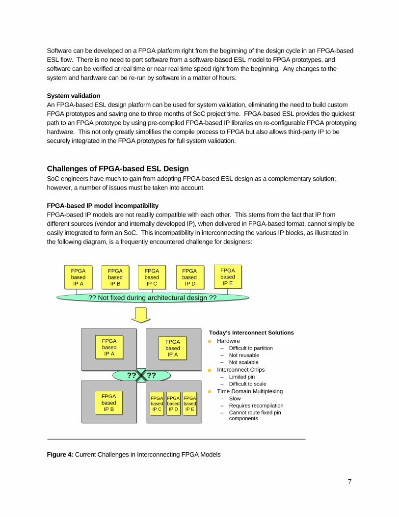
7
Software can be developed on a FPGA platform right from the beginning of the design cycle in an FPGA-based ESL flow. There is no need to port software from a software-based ESL model to FPGA prototypes, and software can be verified at real time or near real time speed right from the beginning. Any changes to the system and hardware can be re-run by software in a matter of hours. System validation An FPGA-based ESL design platform can be used for system validation, eliminating the need to build custom FPGA prototypes and saving one to three months of SoC project time. FPGA-based ESL provides the quickest path to an FPGA prototype by using pre-compiled FPGA-based IP libraries on re-configurable FPGA prototyping hardware. This not only greatly simplifies the compile process to FPGA but also allows third-party IP to be securely integrated in the FPGA prototypes for full system validation. Challenges of FPGA-based ESL Design SoC engineers have much to gain from adopting FPGA-based ESL design as a complementary solution; however, a number of issues must be taken into account. FPGA-based IP model incompatibility FPGA-based IP models are not readily compatible with each other. This stems from the fact that IP from different sources (vendor and internally developed IP), when delivered in FPGA-based format, cannot simply be easily integrated to form an SoC. This incompatibility in interconnecting the various IP blocks, as illustrated in the following diagram, is a frequently encountered challenge for designers:
?? ???? ??
FPGAbasedIP A
FPGAbasedIP A
FPGAbasedIP B
FPGAbasedIP B
FPGAbasedIP C
FPGAbasedIP C
FPGA based IP D
FPGA based IP D
FPGAbasedIP E
FPGAbasedIP E
?? Not fixed during architectural design ???? Not fixed during architectural design ??
FPGAbasedIP A
FPGAbasedIP A
FPGAbasedIP A
FPGAbasedIP A
FPGAbasedIP B
FPGAbasedIP B
FPGAbasedIP C
FPGAbasedIP C
FPGAbasedIP D
FPGAbasedIP D
FPGAbasedIP E
FPGAbasedIP E
Today’s Interconnect SolutionsHardwire
– Difficult to partition– Not reusable– Not scalable
Interconnect Chips– Limited pin– Difficult to scale
Time Domain Multiplexing– Slow– Requires recompilation– Cannot route fixed pin
components
Figure 4: Current Challenges in Interconnecting FPGA Models

8
The industry has resorted to a number of different interconnect technologies to address this incompatibility, though none are without drawbacks: 1) Hardwire The fixed interconnect between FPGAs makes design partitioning difficult, and is neither scalable nor easily reusable. Hardwire cannot achieve the interconnect programmability required for FPGA-based ESL designs. 2) Interconnect chips Although there have been several manufacturers of interconnect chips over the past decade, these chips do not have enough pins to route multiple FPGAs efficiently. Multiple layers of these interconnect chips are required to achieve full programmability but the result is an extremely slow interconnect and unscalable architecture. 3) Time domain multiplexing (TDM) TDM can be pictured as static communication channels that require many clock cycles to create interconnections between FPGAs. The assignments of the static communication channels need to be done before FPGA compilation and therefore is a painful process when the configuration changes frequently, such as when building system-level designs. FPGA models are difficult to analyze Although it is always difficult for designers to debug designs in FPGAs, it is even more difficult to debug FPGA-based IP that they did not create themselves. When an error is discovered in an SoC during the integration stage, the designer must first distinguish whether the error is located at the system level or in one of the many FPGA-based IP within the SoC. With today’s methodology, there is no easy method to debug an FPGA-based system-level design. TAI IP Resolves Deficits of FPGA-based ESL Design TAI IP technology makes FPGA-based ESL design feasible by engendering FPGA-based IP compatibility and analyzability. TAI IP is an encrypted representation of any IP in FPGA netlist format with TAI structure insertions that make the IO of the IP in FPGA dynamically configurable, even in FPGA binary format. As a result, when multiple TAI IP blocks talk to each other, they can be intelligently linked through dynamic communication channels without having to be recompiled when the configuration changes. When using TAI IP in FPGA binary format, switching a TAI IP in or out of a system design on an FPGA platform can potentially be done in just a few minutes by simply changing the system configuration in the software, re-downloading the FPGA, and dynamically configuring the TAI IP blocks. Without the use of TAI IP technology, FPGA-based IP are similar to fixed pin components, and an architect assembling a system out of these components will soon face bus and IO compatibility issues. In most cases, no matter what interconnect technology is used, architects are required to access the IP model at the RTL netlist level, which requires lengthy recompilation that renders system design creation using FPGA-based IP models unfeasible. In contrast, TAI IP provides plug-and-play system configuration on FPGA platforms allowing designers to conveniently evaluate different IP and architectures. In addition, TAI IP embeds system-level analytical information in its database that is essential for ESL designs. Users can pre-define symbols and set events to watch or trigger during the TAI IP creation process. With this information, system architects can efficiently use TAI IP without detailed knowledge of internal IP functionality.
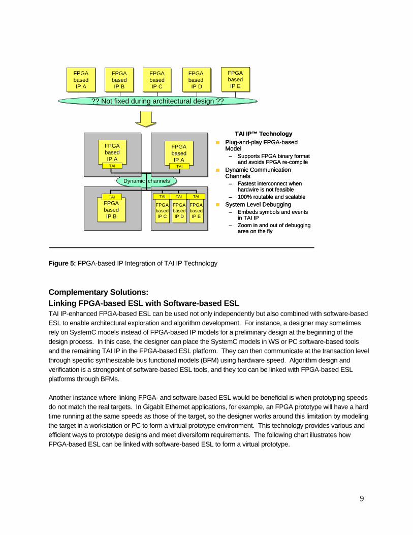
9
Dynamic channelsDynamic channels
FPGAbasedIP A
FPGAbasedIP A
FPGAbasedIP B
FPGAbasedIP B
FPGAbasedIP C
FPGAbasedIP C
FPGA based IP D
FPGA based IP D
FPGAbasedIP E
FPGAbasedIP E
?? Not fixed during architectural design ???? Not fixed during architectural design ??
FPGAbasedIP A
FPGAbasedIP A
FPGAbasedIP A
FPGAbasedIP A
FPGAbasedIP B
FPGAbasedIP B
FPGAbasedIP C
FPGAbasedIP C
FPGAbasedIP D
FPGAbasedIP D
FPGAbasedIP E
FPGAbasedIP E
TAI TAI
TAI IP™ TechnologyPlug-and-play FPGA-based Model
– Supports FPGA binary format and avoids FPGA re-compile
Dynamic Communication Channels
– Fastest interconnect when hardwire is not feasible
– 100% routable and scalable System Level Debugging
– Embeds symbols and events in TAI IP
– Zoom in and out of debugging area on the fly
TAI TAI TAI TAI
Dynamic channelsDynamic channels
FPGAbasedIP A
FPGAbasedIP A
FPGAbasedIP B
FPGAbasedIP B
FPGAbasedIP C
FPGAbasedIP C
FPGA based IP D
FPGA based IP D
FPGAbasedIP E
FPGAbasedIP E
?? Not fixed during architectural design ???? Not fixed during architectural design ??
FPGAbasedIP A
FPGAbasedIP A
FPGAbasedIP A
FPGAbasedIP A
FPGAbasedIP B
FPGAbasedIP B
FPGAbasedIP C
FPGAbasedIP C
FPGAbasedIP D
FPGAbasedIP D
FPGAbasedIP E
FPGAbasedIP E
TAI TAI
TAI IP™ TechnologyPlug-and-play FPGA-based Model
– Supports FPGA binary format and avoids FPGA re-compile
Dynamic Communication Channels
– Fastest interconnect when hardwire is not feasible
– 100% routable and scalable System Level Debugging
– Embeds symbols and events in TAI IP
– Zoom in and out of debugging area on the fly
TAI TAI TAI TAI
Figure 5: FPGA-based IP Integration of TAI IP Technology
Complementary Solutions: Linking FPGA-based ESL with Software-based ESL TAI IP-enhanced FPGA-based ESL can be used not only independently but also combined with software-based ESL to enable architectural exploration and algorithm development. For instance, a designer may sometimes rely on SystemC models instead of FPGA-based IP models for a preliminary design at the beginning of the design process. In this case, the designer can place the SystemC models in WS or PC software-based tools and the remaining TAI IP in the FPGA-based ESL platform. They can then communicate at the transaction level through specific synthesizable bus functional models (BFM) using hardware speed. Algorithm design and verification is a strongpoint of software-based ESL tools, and they too can be linked with FPGA-based ESL platforms through BFMs. Another instance where linking FPGA- and software-based ESL would be beneficial is when prototyping speeds do not match the real targets. In Gigabit Ethernet applications, for example, an FPGA prototype will have a hard time running at the same speeds as those of the target, so the designer works around this limitation by modeling the target in a workstation or PC to form a virtual prototype environment. This technology provides various and efficient ways to prototype designs and meet diversiform requirements. The following chart illustrates how FPGA-based ESL can be linked with software-based ESL to form a virtual prototype.
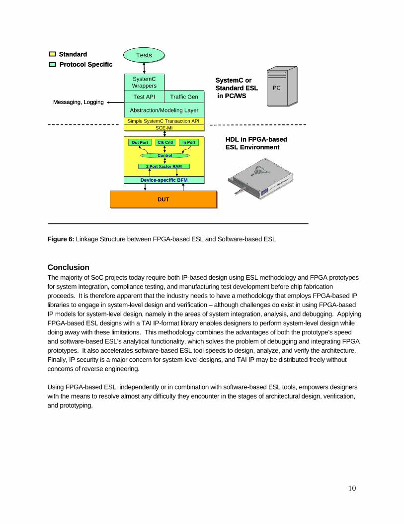
10
SystemCWrappers
Test API
DUTDUT
HDL in FPGA-based ESL Environment
SystemC or Standard ESL in PC/WS
TestsTests
Device-specific BFMDevice-specific BFM
Abstraction/Modeling Layer
Traffic Gen
Simple SystemC Transaction API SCE-MI
Messaging, Logging
StandardProtocol Specific
PCPC
Control
Clk CntlOut Port
2 Port Xactor RAM
In Port
SystemCWrappers
Test API
DUTDUT
HDL in FPGA-based ESL Environment
SystemC or Standard ESL in PC/WS
TestsTests
Device-specific BFMDevice-specific BFM
Abstraction/Modeling Layer
Traffic Gen
Simple SystemC Transaction API SCE-MI
Messaging, Logging
StandardProtocol Specific
PCPC
Control
Clk CntlOut Port
2 Port Xactor RAM
In Port
Figure 6: Linkage Structure between FPGA-based ESL and Software-based ESL Conclusion The majority of SoC projects today require both IP-based design using ESL methodology and FPGA prototypes for system integration, compliance testing, and manufacturing test development before chip fabrication proceeds. It is therefore apparent that the industry needs to have a methodology that employs FPGA-based IP libraries to engage in system-level design and verification – although challenges do exist in using FPGA-based IP models for system-level design, namely in the areas of system integration, analysis, and debugging. Applying FPGA-based ESL designs with a TAI IP-format library enables designers to perform system-level design while doing away with these limitations. This methodology combines the advantages of both the prototype’s speed and software-based ESL’s analytical functionality, which solves the problem of debugging and integrating FPGA prototypes. It also accelerates software-based ESL tool speeds to design, analyze, and verify the architecture. Finally, IP security is a major concern for system-level designs, and TAI IP may be distributed freely without concerns of reverse engineering. Using FPGA-based ESL, independently or in combination with software-based ESL tools, empowers designers with the means to resolve almost any difficulty they encounter in the stages of architectural design, verification, and prototyping.

11
About S2C Inc. Founded and headquartered in San Jose, California, S2C is the leading total solution provider in facilitating systems to chip innovations. S2C has three solutions for system-on-chip (SoC) development:
• Rapid SoC prototyping on Field Programmable Gate Array (FPGA) • Third-party silicon intellectual properties (IP) • SoC design, prototype and production services
S2C’s value proposition is our highly qualified engineering team and customer-focused sales force that understands our customers’ commercial needs in SoC development. S2C’s unique FPGA-based electronic system level (ESL) solution, using our patented TAI IP technology, enables designers who employ silicon IP to quickly assemble SoC prototypes on FPGA easily and securely, thereby enabling customers to start software development, typically the long pole item in development schedules, immediately. Combining rapid prototyping methodologies with a comprehensive portfolio of silicon IP and advanced design solutions, S2C can reduce the SoC design cycle by up to nine months. S2C currently has 3 direct offices located in Shanghai, Beijing and Shenzhen to meet the demand for accelerated SoC design activities in China. S2C is also the organizer of the annual SoCIP symposium in China, which brings SoC designers/professionals from the region and international silicon IP and SoC solution vendors together.