wishbone system-on-chip (soc) interconnection architecture...
TRANSCRIPT
Specification for the:
WISHBONE System-On-Chip (SoC)Interconnection Architecture
for Portable IP Cores
Revision: B.1
Preliminary
Silicore CorporationSilicore CorporationSilicore CorporationSilicore Corporation6310 Butterworth Lane – Corcoran, MN 55340TEL: (763) 478-3567 FAX: (763) 478-3568www.silicore.net Electronic DElectronic DElectronic DElectronic Deeeesignsignsignsign
Sensors Sensors Sensors Sensors •••• IP Cores IP Cores IP Cores IP Cores

WISHBONE SoC Architecture Specification, Revision B 2
This Page is Intentionally Blank

WISHBONE SoC Architecture Specification, Revision B 3
Stewardship
Stewardship for this specification is maintained by Silicore Corporation. Questions, commentsand suggestions about this document are welcome and should be directed to:
Wade D. Peterson, Silicore Corporation6310 Butterworth Lane – Corcoran, MN 55340
TEL: (763) 478-3567; FAX: (763) 478-3568E-MAIL: [email protected] URL: www.silicore.net
Silicore Corporation maintains this document as a service to its customers and to the IP core in-dustry as a whole. The intent of this specification is to improve the quality of Silicore products,as well as to foster cooperation among the users and suppliers of IP cores.
Copyright & Trademark Release / Royalty Release / Patent Notice
Notice is hereby given that this document is not copyrighted, and is in the public domain. It maybe freely copied and distributed by any means.
The term WISHBONE and the WISHBONE compatible logo are not trademark protected. TheWISHBONE logo may be freely used under the compatibility conditions stated elsewhere in thisdocument.
This specification may be used for the design and production of system-on-chip (SoC) compo-nents without royalty or other financial obligation to Silicore Corporation.
The author(s) of this specification are not aware that the information contained herein, nor ofproducts designed to the specification, cause infringement on the patent, copyright, trademark ortrade secret rights of others. However, the possibility exists that such infringement may existwithout their knowledge. The user of this document assumes all responsibility for determining ifproducts designed to this specification infringe on the intellectual property rights of others.
Disclaimers
In no event shall Silicore Corporation be liable for incidental, consequential, indirect, or specialdamages resulting from the use of this specification. By adopting this specification, the user as-sumes all responsibility for its use or misuse.
This is a preliminary document, and is subject to change.
Silicore is a registered service mark and trademark of Silicore Corporation.Verilog is a registered trademark of Cadence Design Systems, Inc.

WISHBONE SoC Architecture Specification, Revision B 4
Document Format, Binding and Covers
This document is formatted for printing on double sided, 8½” x 11” white paper stock. It is de-signed to be bound within a standard cover. The preferred binding method is a black coil bind-ing with outside diameter of 9/16” (14.5 mm). The preferred cover stock is Paper Direct partnumber KVR09D (forest green) and is available on-line at: www.paperdirect.com. Binding canbe performed at most full-service copy centers such as Kinkos (www.kinkos.com).
Revision History
Revision A (preliminary) - June 16, 1999Original specification release.
Revision A.1 (preliminary) - Updated July 27, 1999Correct typographical errors.
Revision B (preliminary) – Updated January 5, 2001Incorporate feedback from users. Clarify use of acknowledge and TAG signals. Add[TAGN_O] signal to SLAVE and [TAGN_I] to MASTER. Correct typographical errors.Change name from ‘WISHBONE Interconnection Architecture For Portable IP Cores’ to‘WISHBONE System-On-Chip (SoC) Interconnection Architecture for Portable IP Cores’. Add‘WISHBONE COMPATIBLE’ logo. Standardize printing and covers, Change standard font toTimes New Roman 12 pt. Change ‘WISHBONE’ to all capital letters. Change steward address.Add appendcies with application notes. Move the glossary to chapter 1. Add an index. Refor-mat under Adobe Acrobat with bookmarks.
Revision B.1 (preliminary) – Updated January 8, 2001Remove all copyright notices and place into the public domain.

WISHBONE SoC Architecture Specification, Revision B 5
Table of Contents
CHAPTER 1 - INTRODUCTION............................................................................................................................. 6
1.1 WISHBONE FEATURES ...................................................................................................................................... 71.2 WISHBONE OBJECTIVES ................................................................................................................................... 91.3 SPECIFICATION TERMINOLOGY .......................................................................................................................... 111.4 USE OF TIMING DIAGRAMS ................................................................................................................................ 121.5 SIGNAL NAMING CONVENTIONS ........................................................................................................................ 141.6 WISHBONE LOGO ........................................................................................................................................... 141.7 GLOSSARY OF TERMS ........................................................................................................................................ 14
CHAPTER 2 – INTERFACE SPECIFICATION .................................................................................................. 21
2.1 REQUIRED DOCUMENTATION FOR IP CORES...................................................................................................... 212.2 WISHBONE SIGNAL DESCRIPTION .................................................................................................................. 22
CHAPTER 3 – BUS INTERFACE.......................................................................................................................... 27
3.1 GENERAL OPERATION........................................................................................................................................ 273.2 SINGLE READ / WRITE CYCLES ................................................................................................................... 323.3 BLOCK READ / WRITE CYCLES.................................................................................................................... 373.4 RMW CYCLE.................................................................................................................................................... 443.5 DATA ORGANIZATION........................................................................................................................................ 47
CHAPTER 4 – TIMING SPECIFICATION .......................................................................................................... 56
CHAPTER 5 – APPLICATION INTERFACE...................................................................................................... 58
5.1 INTERCONNECTION METHODS ........................................................................................................................... 585.2 THREE-STATE INTERCONNECTIONS ................................................................................................................... 615.3 ENDIAN CONVERSION ........................................................................................................................................ 62
REFERENCES.......................................................................................................................................................... 63
APPENDIX A – WISHBONE DESIGN PHILOSOPHY ...................................................................................... 64
APPENDIX B - WISHBONE INTERFACE FOR SLAVE I/O PORTS.............................................................. 76
APPENDIX C - WISHBONE INTERFACE FOR MEMORY ELEMENTS...................................................... 83
INDEX........................................................................................................................................................................ 86

WISHBONE SoC Architecture Specification, Revision B 6
Chapter 1 - Introduction
The WISHBONE1 System-On-Chip (SoC) Interconnection Architecture for Portable IP Cores isa flexible design methodology for use with semiconductor IP cores. Its purpose is to foster de-sign reuse by alleviating system-on-chip integration problems. This is accomplished by creatinga common interface between IP cores. This improves the portability and reliability of the sys-tem, and results in faster time-to-market for the end user.
Previously, IP cores used non-standard interconnection schemes that made them difficult to inte-grate. This required the creation of custom glue logic to connect each of the cores together. Byadopting a standard interconnection scheme, the cores can be integrated more quickly and easilyby the end user.
This specification can be used for soft core, firm core or hard core IP. Since firm and hard coresare generally conceived as soft cores, the specification is written from that standpoint.
This specification does not require the use of specific development tools or target hardware.Furthermore, it is fully compliant with virtually all logic synthesis tools. However, the examplespresented in the specification do use the VHDL hardware description language. These are pre-sented only as a convenience to the reader, and should be readily understood by users of otherhardware description languages (such as Verilog). Schematic based tools can also be used.
The WISHBONE interconnect is intended as a general purpose interface. As such, it defines thestandard data exchange between IP core modules. It does not attempt to regulate the application-specific functions of the IP core.
The WISHBONE architects were strongly influenced by three factors. First, there was a need fora good, reliable system-on-chip integration solution. Second, there was a need for a commoninterface specification to facilitate structured design methodologies on large project teams.Third, they were impressed by the traditional system integration solutions afforded by micro-computer buses such as PCI bus and VMEbus.
In fact, the WISHBONE architecture is analogous to a microcomputer bus in that that they both:(a) offer a flexible integration solution that can be easily tailored to a specific application; (b)offer a variety of bus cycles and data path widths to solve various system problems; and (c) al-low products to be designed by a variety of suppliers (thereby driving down price while improv-ing performance and quality).
1 Webster’s dictionary defines a WISHBONE as “the forked clavicle in front of the breastbone of most birds.” Theterm ‘WISHBONE interconnect’ was coined by Wade Peterson of Silicore Corporation. During the initial definitionof the scheme he was attempting to find a name that was descriptive of a bi-directional data bus that used eithermultiplexors or three-state logic. This was solved by forming an interface with separate input and output paths.When these paths are connected to three-state logic it forms a ‘Y’ shaped configuration that resembles a wishbone.The actual name was conceived during a Thanksgiving Day dinner that included roast turkey. Thanksgiving Day isa national holiday in the United States, and is observed on the third Thursday in November. It is generally cele-brated with a traditional turkey dinner.

WISHBONE SoC Architecture Specification, Revision B 7
However, traditional microcomputer buses are fundamentally handicapped for use as a system-on-chip interconnection. That’s because they are designed to drive long signal traces and con-nector systems which are highly inductive and capacitive. In this regard, system-on-chip is muchsimpler and faster. Furthermore, the system-on-chip solutions have a rich set of interconnectionresources. These do not exist in microcomputer buses because they are limited by IC packagingand mechanical connectors.
The WISHBONE architects have attempted to create a specification that is robust enough to in-sure complete compatibility between IP cores. However, it has not been over specified so as tounduly constrain the creativity of the core developer or the end user. It is believed that these twogoals have been accomplished with the publication of this document.
1.1 WISHBONE Features
The WISHBONE interconnection makes system-on-chip and design reuse easy by creating astandard data exchange protocol. Features of this technology include:
• Simple, compact, logical IP core hardware interfaces require very few logic gates.
• Supports structured design methodologies used by large project teams.
• Full set of popular data transfer bus protocols including:
- READ/WRITE cycle- BLOCK transfer cycle- RMW cycle- EVENT cycle
• Data bus widths2 and operand sizes up to 64-bits.
• Supports both BIG ENDIAN and LITTLE ENDIAN data ordering.
• Variable core interconnection method supports memory mapped, FIFO memory andcrossbar interconnections.
• Handshaking protocol allows each core to throttle data transfer speed.
• Supports single clock data transfers.
• Supports normal cycle termination, retry termination and termination due to error.
2 Specifications are given for data port and operand sizes up to 64-bits. However, the basic architecture can theo-retically support any data width (e.g. 128-bit, 256-bit etc.). Also, zero bit data bus accesses are permissible (forevent cycles).

WISHBONE SoC Architecture Specification, Revision B 8
• Address widths3 up to 64-bits.
• Partial address decoding scheme for slaves. This facilitates high speed address decod-ing, uses less redundant logic and supports variable address sizing and interconnectionmeans.
• User-defined tag support. This is useful for identifying data transfers such as:
- Data transfers- Interrupt vectors- Cache control operations
• MASTER / SLAVE architecture for very flexible system designs.
• Multiprocessing (multi-MASTER) capabilities. This allows for a wide variety of sys-tem-on-chip configurations, including:
- Single MASTER / single SLAVE- Multiple MASTER / single SLAVE- Single MASTER / multiple SLAVE- Multiple MASTER / multiple SLAVE- Crossbar switches
• Arbitration methodology is defined by the end user (priority arbiter, round-robin arbi-ter, etc.).
• Supports various IP core interconnection means, including:
- Unidirectional bus- Bi-directional bus- Multiplexor based interconnections- Three-state based interconnections- Off chip I/O
• Synchronous design assures portability, simple design and ease of test.
• Very simple, variable timing specification.
• Documentation requirements allow the end user to quickly evaluate interface needs.
• Independent of hardware technology (FPGA, ASIC, etc.).
• Independent of delivery method (soft, firm or hard core).
3 Specifications are given for address widths between zero and 64-bits. However, the basic architecture can theo-retically support any address width.

WISHBONE SoC Architecture Specification, Revision B 9
• Independent of synthesis tool, router and layout tool technology.
• Independent of FPGA and ASIC test methodologies.
• Seamless design progression between FPGA prototypes and ASIC production chips.
1.2 WISHBONE Objectives
The main objective of the specification is to create a flexible interconnection means for use withsemiconductor IP cores. This allows various IP core modules to be connected together to form asystem-on-chip.
A further objective of the specification is to enforce good compatibility between IP core mod-ules. This enhances design reuse.
A further objective of the specification is to create a robust standard, but one that does not un-duly constrain the creativity of the core developer or the end user.
A further objective of the specification is to make it easy to understand by both the core devel-oper and the end user.
A further objective of the specification is to facilitate structured design methodologies on largeproject teams. With structured design, individual team members can build and test small parts ofthe design. Each member of the design team can interface to the common, well-defined WISH-BONE specification. When all of the sub-assemblies have been completed, the full system canbe integrated.
A further objective of the specification is create a portable interface that is independent of theunderlying semiconductor technology. For example, the interconnect must be capable of work-ing with both FPGA and ASIC hardware target devices.
A further objective of the specification is to make the interface independent of logic signalinglevels.
A further objective of the specification is to create a flexible interconnection scheme that is inde-pendent of the IP core delivery method. For example, it may be used with ‘soft core’, ‘firm core’or ‘hard core’ delivery methods.
A further objective of the specification is to be independent of the underlying hardware descrip-tion. For example, soft cores may be written and synthesized in VHDL, Verilog or some otherhardware description language. Schematic entry may also be used.
A further objective of the specification is to require a minimum standard for documentation.This allows IP core users to quickly evaluate and integrate new cores.

WISHBONE SoC Architecture Specification, Revision B 10
A further objective of the specification is to eliminate extensive interface documentation on thepart of the IP core developer. In most cases, this specification along with the WISHBONE DA-TASHEET is sufficient to completely document an IP core interface.
A further objective is to create an architecture that has a smooth transition path to support newtechnologies. This increases the longevity of the specification as it can adapt to new, and as yetun-thought-of, requirements.
A further objective is to create an architecture that allows various interconnection means be-tween IP core modules. This insures that the end user can tailor the system-on-chip to his/herown needs.
A further objective is to create an architecture that requires a minimum of glue logic. In somecases the system-on-chip needs no glue logic whatsoever. However, in other cases the end usermay choose to use a more sophisticated interconnection method (for example with FIFO memo-ries or crossbar switches) that requires additional glue logic.
A further objective is to create an architecture with variable address and data path widths to meeta wide variety of system requirements.
A further objective is to create an architecture that supports both BIG ENDIAN and LITTLEENDIAN data transfer organizations.
A further objective is to create an architecture that supports one data transfer per clock cycle.
A further objective is to create an architecture that allows data to be tagged. This allows the pur-pose for each bus cycle to be identified by a SLAVE. For example, in microprocessor basedsystems it is often necessary to discriminate between data transfer, interrupt acknowledge andcaching operations.
A further objective is to create an architecture with a MASTER/SLAVE topology. Furthermore,the system must be capable of supporting multiple MASTERs and multiple SLAVEs with an ef-ficient arbitration mechanism.
A further objective is to create an architecture that supports crossbar switches.
A further objective is to create a synchronous protocol to insure ease of use, good reliability andeasy testing. Furthermore, all transactions can be coordinated by a single clock.
A further objective is to create a synchronous protocol that works over a wide range of interfaceclock speeds. The effects of this are: (a) that the WISHBONE interface can work synchronouslywith all attached IP cores, (b) that the interface can be used on a large range of target devices, (c)that the timing specification is much simpler and (d) that the resulting semiconductor device ismuch more testable.

WISHBONE SoC Architecture Specification, Revision B 11
A further objective is to create a synchronous protocol that provides a simple timing specifica-tion. This makes the interface very easy to integrate.
A further objective is to create a synchronous protocol where each MASTER and SLAVE canthrottle the data transfer rate with a handshaking mechanism.
A further objective is to create a synchronous protocol where data may be transferred throughmemory mapped, FIFO memory or crossbar switch interconnections.
A further objective is to create a synchronous protocol that is optimized for system-on-chip, butthat is also suitable for off-chip I/O routing. Generally, the off-chip WISHBONE interconnectwill operate at slower speeds.
1.3 Specification Terminology
To avoid confusion, and to clarify the requirements for compliance, this specification makes useof five keywords to define the operation of the WISHBONE interconnect. The keywords are:
• RULE• RECOMMENDATION• SUGGESTION• PERMISSION• OBSERVATION
Any text not labeled with one of these keywords describes the operation in a narrative style. Thekeywords are defined as follows:
RULERules form the basic framework of the specification. They are sometimes expressed in text formand sometimes in the form of figures, tables or drawings. All rules MUST be followed to ensurecompatibility between interfaces. Rules are characterized by an imperative style. The upper-case words MUST and MUST NOT are reserved exclusively for stating rules in this document,and are not used for any other purpose.
RECOMMENDATIONWhenever a recommendation appears, designers would be wise to take the advice given. Doingotherwise might result in some awkward problems or poor performance. While this specificationhas been designed to support high performance systems, it is possible to create an interconnec-tion that complies with all the rules, but has very poor performance. In many cases a designerneeds a certain level of experience with the system architecture in order to design interfaces thatdeliver top performance. Recommendations found in this document are based on this kind ofexperience and are provided as guidance for the user.

WISHBONE SoC Architecture Specification, Revision B 12
SUGGESTIONA suggestion contains advice which is helpful but not vital. The reader is encouraged to considerthe advice before discarding it. Some design decisions are difficult until experience has beengained. Suggestions help a designer who has not yet gained this experience. Some suggestionshave to do with designing compatible interconnections, or with making system integration easier.
PERMISSIONIn some cases a rule does not specifically prohibit a certain design approach, but the reader mightbe left wondering whether that approach might violate the spirit of the rule, or whether it mightlead to some subtle problem. Permissions reassure the reader that a certain approach is accept-able and will not cause problems. The upper-case word MAY is reserved exclusively for statinga permission and is not used for any other purpose.
OBSERVATIONObservations do not offer any specific advice. They usually clarify what has just been discussed.They spell out the implications of certain rules and bring attention to things that might otherwisebe overlooked. They also give the rationale behind certain rules, so that the reader understandswhy the rule must be followed.
1.4 Use of Timing Diagrams
Figure 1-1 shows some of the key features of the timing diagrams in this specification. Unlessotherwise noted, the MASTER signal names are referenced in the timing diagrams. In somecases the MASTER and SLAVE signal names are different. For example, in the single MAS-TER / single SLAVE configuration, the [ADR_O] and [ADR_I] signals are connected together.Furthermore, the actual waveforms at the SLAVE may vary from those at the MASTER. That’sbecause the MASTER and SLAVE interfaces can be connected together in different ways. Un-less otherwise noted, the timing diagrams refer to the connection diagram shown in Figure 1-2.
Figure 1-1. Use of timing diagrams.
CLK_I 10
ADR_O() VALID
-WSS-
Signal Name
Signal LevelUndefined
Clock EdgeTransition
Point
Edge Number
Stable, Valid Data
Wait State

WISHBONE SoC Architecture Specification, Revision B 13
Figure 1-2. Standard connection for timing diagrams.
Individual signals may or may not be present on an specific interface. That’s because most ofthe signals are optional.
Two symbols are also presented in relation to the [CLK_I] signal. These include the positivegoing clock edge transition point and the clock edge number. In most diagrams a vertical guide-line is shown at the positive-going edge of each [CLK_I] transition. This represents the theoreti-cal transition point at which flip-flops register their input value, and transfer it to their output.The exact level of this transition point varies depending upon the technology used in the targetdevice. The clock edge number is included as a convenience so that specific points in the timingdiagram may be referenced in the text. The clock edge number in one timing diagram is not re-lated to the clock edge number in another diagram.
Gaps in the timing waveforms may be shown. These indicate either: (a) a wait state or (b) a por-tion of the waveform that is not of interest (in the context of the diagram). When the gap indi-cates a wait state, the symbols ‘-WSM-‘ or ‘-WSS-‘ are placed in the gap along the [CLK_I]waveform. These correspond to wait states inserted by the MASTER or SLAVE interfaces.
Undefined signal levels are indicated by a hatched region. In MASTER interfaces, this regionindicates that the signal level is undefined, and may take any state. In SLAVE interfaces, thisregion indicates that the current state is undefined, and should not be relied upon. When signalarrays are used, stable and predictable signal levels are indicated with the word ‘VALID’. Non-array signals show a steady high or low state.
CLK_IADR_O()DAT_I()
DAT_O()WE_O
SEL_O()STB_OACK_I
CLK_IADR_I()DAT_I()
DAT_O()WE_ISEL_I()STB_IACK_O
WISHBONE MASTER
WISHBONE SLAVE
CYC_O CYC_ITAGN_O TAGN_I
RST_I RST_I
TAGN_I TAGN_OUSER
DEFINED
SYSCON

WISHBONE SoC Architecture Specification, Revision B 14
1.5 Signal Naming Conventions
All signal names used in this specification have the ‘_I’ or ‘_O’ characters attached to them.These indicate if the signals are an input (to the core) or an output (from the core). For example,[ACK_I] is an input and [ACK_O] is an output. This convention is used to clearly identify thedirection of each signal.
In some cases, the input and output characters ‘I’ and ‘O’ may be omitted and replaced by an‘X’. For example: [TAG3_X]. This is not an actual signal name, but rather a shorthand form toindicate both the [TAG3_I] and [TAG3_O] signal.
Signal arrays are identified by a name followed by the array boundaries in parenthesis. For ex-ample, [DAT_I(63..0)] is a signal array with upper array boundary number sixty-three, and lowerarray boundary number zero. Furthermore, the array boundaries indicate the full range of thepermissible array size. The array size on any particular core may vary. In many cases the arrayboundaries are omitted if they are irrelevant to the context of the description.
When used as part of a sentence, signal names are enclosed in brackets ‘[ ]’. This helps to dis-criminate signal names from the words in the sentence.
1.6 WISHBONE Logo
The WISHBONE logo can be affixed to SoC documents that are compatible with this standard.Figure 1-3 shows the logo.
Figure 1-3. WISHBONE logo.
PERMISSION 1.10Documents describing a WISHBONE compatible SoC component that are 100% compliant withthis standard, MAY use the WISHBONE logo.
1.7 Glossary of Terms
0x (prefix)The ‘0x’ prefix indicates a hexadecimal number. It is the same nomenclature as commonly usedin the UNIX operating system.

WISHBONE SoC Architecture Specification, Revision B 15
Active High Logic StateA logic state that is ‘true’ when the logic level is a binary ‘1’. The high state is at a higher volt-age than the low state.
Active Low Logic StateA logic state that is ‘true’ when the logic level is a binary ‘0’. The low state is at a lower voltagethan the high state.
ASICAcronym for: Application Specific Integrated Circuit. General term which describes a genericarray of logic gates or analog building blocks which are programmed by a metalization layer at asilicon foundry. High level circuit descriptions are impressed upon the logic gates or analogbuilding blocks in the form of metal interconnects.
AssertedA verb indicating that a logic state as switched from the inactive state to the active state. Whenactive high logic is used it means that a signal has switched from a low logic level to a high logiclevel.
BusA common group of paths over which input and output signals are routed.
Bus InterfaceAn electronic circuit that drives or receives data from a bus.
Crossbar Interconnect (Switch)Crossbar switches are mechanisms that allow IP cores to connect and communicate. Each con-nection channel can be operated in parallel to other connection channels. This increases the datatransfer rate of the entire system by employing parallelism. Stated another way, two 100Mbyte/second channels can operate in parallel, thereby providing a 200 Mbyte/second transferrate. This makes the crossbar switches inherently faster than traditional bus schemes. Crossbarrouting mechanisms generally support dynamic configuration. This creates a configurable andreliable network system. Most crossbar architectures are also scalable, meaning that families ofcrossbars can be added as the needs arise.
Data OrganizationThe ordering of data during a transfer. Generally, 8-bit (byte) data can be stored with the mostsignificant byte of a mult-byte transfer at the higher or the lower address. These two methods aregenerally called BIG ENDIAN and LITTLE ENDIAN, respectively. In general, BIG ENDIANrefers to byte lane ordering where the most significant byte is stored at the lower address. LIT-TLE ENDIAN refers to byte lane ordering where the most significant byte is stored at the higheraddress. The terms BIG ENDIAN and LITTLE ENDIAN for data organization was coined byDanny Cohen of the Information Sciences Institute, and was derived from the book Gulliver’sTravels by Jonathan Swift (see references).

WISHBONE SoC Architecture Specification, Revision B 16
ENDIANSee the definition under ‘Data Organization’.
FIFO MemoryAcronym for: First In First Out. A type of memory used to transfer data between ports on twodevices. The first data loaded into the FIFO by an output port on one device is the first data readby an input port on another device. The FIFO memory is very useful for interconnecting cores ofdiffering speeds.
Fixed InterconnectionA microcomputer bus interconnection that is fixed, and cannot be changed without causing in-compatibilities between bus modules (or SoC/IP cores). Also called a static interconnection.Examples of fixed interconnection buses include PCI, cPCI and VMEbus. Also see variable in-terconnection.
Fixed Timing SpecificationA microcomputer bus timing specification that is based upon a fixed set of rules. Generally usedin traditional microcomputer buses like PCI and VMEbus. Each bus module must conform tothe ridged set of timing specifications.
FoundrySee silicon foundry.
FPGAAcronym for: Field Programmable Gate Array. Generally describes a generic array of logicalgates and interconnect paths which are programmed by the end user. High level logic descrip-tions are impressed upon the gates and interconnect paths, often in the form of IP Cores.
Full Address DecodingA method of address decoding where each slave decodes all of the available address space. Forexample, if a 32-bit address bus is used, then each slave module decodes all thirty-two addressbits. This technique is used on standard microcomputer buses like PCI and VMEbus. Also seepartial address decoding.
Glue LogicLogic gates and interconnections required to connect IP cores together. The requirements forglue logic vary greatly depending upon the interface requirements of the IP cores.
GranularityThe smallest unit of data transfer that a port is capable of transferring. For example, a 32-bit portcan be broken up into four 8-bit BYTE segments. In this case, the granularity of the interface is8-bits. Also see port size and operand size.
HDLAcronym for: Hardware Description Language. Examples include VHDL and Verilog.
WISHBONE SoC Architecture Specification, Revision B 17
IP CoreAcronym for: Intellectual Property Core. Also see ‘soft core’, ‘firm core’ and ‘hard core’.
MASTERA WISHBONE interface that is capable of generating bus cycles. All systems based on theWISHBONE interconnect must have at least one SLAVE.
Memory Mapped AddressingAn architecture that allows memory to be stored and recalled at individual, binary addresses.
ModuleIn the context of this specification, it’s another name for anIP core.
Multiplexor Logic InterconnectionA microcomputer bus interconnection that uses multiplexors to route address, data and controlsignals. Often used for system-on-chip (SoC) applications. Also see three-state bus intercon-nection.
NegatedA verb indicating that a logic state as switched from the active state to the inactive state. Whenactive high logic is used it means that a signal has switched from a high logic level to a low logiclevel. Also see asserted.
Operand SizeThe operand size is the largest single unit of data transfer that will be moved through the inter-face. For example, a 32-bit DWORD operand can be moved through an 8-bit port with four datatransfers. Also see granularity and port size.
Partial Address DecodingA method of address decoding where each slave decodes only the range of addresses that it re-quires. For example, if the module has only four registers, then it decodes only two address bits.This technique is used on SoC microcomputer buses, and has the advantages of: less redundantlogic in the system, it supports variable address buses, it supports variable interconnection busesand is relatively fast. Also see partial address decoding.
PCIAcronym for: Peripheral Component Interconnect. Generally used as an nterconnection schemebetween chips. While this specification is very flexible, it isn’t practical for system-on-chip ap-plications because if it’s large size and slow speed.
Port SizeThe width of the WISHBONE data ports in bits. Also see granularity and operand size.
RouterA software tool that physically routes interconnection paths between logic gates. Applies toFPGA and ASIC devices.
WISHBONE SoC Architecture Specification, Revision B 18
RTL Design MethodologyA design methodology that uses register-transfer-logic (RTL) concepts. This design methodol-ogy moves data between registers. Data is latched in the registers at one or more stages alongthe path of signal propagation. The WISHBONE specification uses a synchronous RTL designmethodology which means that each register is clocked with a common clock.
Silicon FoundryA factory that produces integrated circuits.
SLAVEA WISHBONE interface that is capable of receiving bus cycles. All systems based on theWISHBONE interconnect must have at least one SLAVE.
SoCAcronym for System-on chip. See also System-on-chip.
Structured DesignA popular design practice used by large project teams. When structured design practices areused, individual team members build and test small parts of the design with a common set oftools. Each sub-assembly is designed to a common standard. When all of the sub-assemblieshave been completed, the full system can be integrated and tested. This approach makes it mucheasier to manage complex projects.
SYSCONA WISHBONE functional module that drives the system clock [CLK_O] and reset [RST_O]signals.
System-on-chipThe ability to create whole systems on a single integrated circuit. In many cases, this requiresthe use of IP cores which have been designed by various IP core providers and individuals.System-on-chip is similar to traditional microcomputer bus systems whereby the individualcomponents are designed, tested and built separately. The components are then integrated toform a finished system.
Target DeviceThe semiconductor type (or technology) onto which the IP core design is impressed. Typicalexamples include FPGA and ASIC devices.
Three-State Bus InterconnectionA microcomputer bus interconnection that relies upon three-state bus drivers. Often used to re-duce the number of interconnecting signal paths through connector and IC pins. Three statebuffers can assume a logic low state (‘0’ or ‘L’), a logic high state (‘1’ or ‘H’) or a high imped-ance state. Three-state buffers are sometimes called Tri-State buffers. Tri-State is a regis-tered trademark of National Instruments Corporation. Also see multiplexor logic interconnec-tion.

WISHBONE SoC Architecture Specification, Revision B 19
Variable InterconnectionA microcomputer bus interconnection that can be changed without causing incompatibilitiesbetween bus modules (or SoC/IP cores). Also called a dynamic interconnection. An example ofa variable interconnection bus is the WISHBONE SoC architecture. Also see fixed interconnec-tion.
Variable Timing SpecificationA microcomputer bus timing specification that is not fixed, and can vary between implementa-tions. Used in SoC buses like WISHBONE. When used in SoC applications, the timing specifi-cations are dictated by the system integrator, and are enforced by integration software such asplace-and-route tools.
VerilogA textual based computer language intended for use in circuit design. The VHDL language isboth a synthesis and a simulation tool. Verilog was originally a proprietary language first con-ceived in 1983 at Gateway Design Automation (Acton, MA), and was later refined by CadenceCorporation. It has since been greatly expanded and refined, and much of it has been placed intothe public domain. Complete descriptions of the language can be found in the IEEE 1364 speci-fication and elsewhere.
VHDLAcronym for: VHSIC Hardware Description Language. [VHSIC: Very High Speed IntegratedCircuit]. A textual based computer language intended for use in circuit design. The VHDL lan-guage is both a synthesis and a simulation tool. Early forms of the language emerged from USDept. of Defense ARPA projects in the 1960’s, and have since been greatly expanded and re-fined. Complete descriptions of the language can be found in the IEEE 1076, IEEE 1073.3,IEEE 1164 specifications and elsewhere.
VMEbusAcronym for: Versa Module Eurocard bus. A popular microcomputer (board) bus. While thisspecification is very flexible, it isn’t practical for system-on-chip applications because if it’slarge size and slow speed.
WISHBONE DATASHEETDocumentation must be provided for each IP core with a WISHBONE interconnect. This helpsthe end user understand the operation of the core, and how to connect it to other cores. Thedocumentation takes the form of a WISHBONE DATASHEET. This can be included in a tech-nical reference manual for the IP core.
WISHBONE SignalA signal that is defined as part of the WISHBONE interface. Non-WISHBONE signals can alsobe used on the IP core, but are not defined as part of this specification. For example, [ACK_O]is a WISHBONE signal, but [CLK100_I] is not.

WISHBONE SoC Architecture Specification, Revision B 20
WISHBONE LogoA logo that, when affixed to a document, indicates that the associated SoC component is com-patible with the WISHBONE standard.
WISHBONE SoC Architecture Specification, Revision B 21
Chapter 2 – Interface Specification
This chapter describes the signaling method between MASTER and SLAVE modules. This in-cludes numerous options which may or may not be present on a particular interface. Further-more, it describes a minimum level of required documentation that must be created for each IPcore.
2.1 Required Documentation for IP Cores
WISHBONE compatible IP cores must include documentation that describes the interface. Thishelps the end user understand the operation of the core, and how to connect it to other cores.This documentation takes the form of a WISHBONE DATASHEET. It can be included as partof the IP core technical reference manual, it can be embedded in source code or it can take otherforms as well.
RULE 2.10Each WISHBONE compatible IP core MUST include a WISHBONE DATASHEET as part ofthe IP core documentation.
RULE 2.11The WISHBONE DATASHEET MUST include the revision level of the WISHBONE specifi-cation to which it was designed.
RULE 2.20The WISHBONE DATASHEET MUST include the signal names that are defined for a WISH-BONE SoC component. If a signal name is different than defined in this specification then itMUST be cross-referenced to the corresponding signal name which is used in this specification.
PERMISSION 2.10Any signal name MAY be used to describe the WISHBONE signals.
RULE 2.30Signal names MUST adhere to the rules of the native tool in which the IP core is designed.
OBSERVATION 2.10Most hardware description languages (such as VHDL or Verilog) have naming conventions.For example, the VHDL hardware description language defines the alphanumeric symbols whichmay be used. Furthermore, it states that UPPERCASE and LOWERCASE characters may beused in a signal name.

WISHBONE SoC Architecture Specification, Revision B 22
RECOMENDATION 2.10It is recommended that the interface use the signal names that are defined in this document.
OBSERVATION 2.20Core integration is simplified if the signal names match those given in this specification. How-ever, in some cases (such as IP cores with multiple WISHBONE interconnects) they cannot beused. The use of non-standard signal names will not result in any serious integration problemssince all hardware description tools allow signals to be renamed.
RULE 2.40All WISHBONE interface signals MUST use active high logic.
PERMISSION 2.11Non-WISHBONE signals MAY be used with IP cores.
OBSERVATION 2.21Most IP cores will include non-WISHBONE signals. These are outside the scope of this specifi-cation, and no attempt is made to govern them. For example, a disk controller IP core couldhave a WISHBONE interface on one end and a disk interface on the other. In this case the speci-fication does not dictate any technical requirements of the disk interface signals. However, itdoes require that the operation of these other signals be documented in the WISHBONE DA-TASHEET.
OBSERVATION 2.22[TAGN_I] and [TAGN_O] are user defined signals that must adhere to the timing specificationsgiven in this document.
2.2 WISHBONE Signal Description
This section describes the signals used in the WISHBONE interconnect. Some of these signalsare optional, and may or may not be present on a specific interface.
2.2.1 SYSCON Signals
CLK_OThe clock output [CLK_O] coordinates all activities for the internal logic within the WISH-BONE interconnect. It is connected to the [CLK_I] input on MASTER and SLAVE modules.

WISHBONE SoC Architecture Specification, Revision B 23
RST_OThe reset output [RST_O] forces the WISHBONE interface to restart. Furthermore, all internalself-starting state machines will be forced into an initial state. It is connected to [RST_I] onMASTER and SLAVE modules.
2.2.2 Signals Common to MASTER and SLAVE Interfaces
CLK_IThe clock input [CLK_I] coordinates all activities for the internal logic within the WISHBONEinterconnect. All WISHBONE output signals are registered at the rising edge of [CLK_I]. AllWISHBONE input signals must be stable before the rising edge of [CLK_I].
RST_IThe reset input [RST_I] forces the WISHBONE interface to restart. Furthermore, all internalself-starting state machines will be forced into an initial state.
TAGN_IThe tag input(s) [TAGN_I] are user defined, and are used with either MASTER or SLAVE inter-faces. ‘N’ in this signal name refers to a tag number because multiple tags may be used (e.g.[TAG3_I]). Tag inputs are used whenever an IP core needs specific information from the inter-connection. For example, a MASTER can be designed to monitor the state of a FIFO.
TAGN_OThe tag output(s) [TAGN_O] are user defined, and are used with either MASTER or SLAVEinterfaces. For example, the tag output(s) can be used to indicate the type of data transfer in pro-gress. Furthermore, ‘N’ in this signal name refers to a tag number because multiple tags may beused. For example, [TAG1_O] may indicate a valid data transfer cycle, [TAG2_O] may indicatean interrupt acknowledge cycle and so on. The exact meaning of each tag is defined by the IPcore provider in the WISHBONE DATASHEET.
2.2.3 MASTER Signals
ACK_IThe acknowledge input [ACK_I], when asserted, indicates the termination of a normal bus cycle.Also see the [ERR_I] and [RTY_I] signal descriptions.

WISHBONE SoC Architecture Specification, Revision B 24
ADR_O(63..0)The address output array [ADR_O(63..0)] is used to pass a binary address, with the most signifi-cant address bit at the higher numbered end of the signal array. The lower array boundary isspecific to the data port size. The higher array boundary is core-specific. In some cases (such asFIFO interfaces) the array may not be present on the interface.
CYC_OThe cycle output [CYC_O], when asserted, indicates that a valid bus cycle is in progress. Thesignal is asserted for the duration of all bus cycles. For example, during a BLOCK transfer cyclethere can be multiple data transfers. The [CYC_O] signal is asserted during the first data trans-fer, and remains asserted until the last data transfer. The [CYC_O] signal is useful for interfaceswith multi-port interfaces (such as dual port memories). In these cases, the [CYC_O] signal re-quests use of a common bus from an arbiter. Once the arbiter grants the bus to the MASTER, itis held until [CYC_O] is negated.
DAT_I(63..0)The data input array [DAT_I(63..0)] is used to pass binary data. The array boundaries are de-termined by the port size. Also see the [DAT_O(63..0)] and [SEL_O(7..0)] signal descriptions.
DAT_O(63..0)The data output array [DAT_O(63..0)] is used to pass binary data. The array boundaries are de-termined by the port size. Also see the [DAT_I(63..0)] and [SEL_O(7..0)] signal descriptions.
ERR_IThe error input [ERR_I] indicates an abnormal cycle termination. The source of the error, andthe response generated by the MASTER is defined by the IP core supplier in the WISHBONEDATASHEET. Also see the [ACK_I] and [RTY_I] signal descriptions.
RTY_IThe retry input [RTY_I] indicates that the indicates that the interface is not ready to accept orsend data, and that the cycle should be retried. When and how the cycle is retried is defined bythe IP core supplier in the WISHBONE DATASHEET. Also see the [ERR_I] and [RTY_I] sig-nal descriptions.
SEL_O(7..0)The select output array [SEL_O(7..0)] indicates where valid data is expected on the[DAT_I(63..0)] signal array during READ cycles, and where it is placed on the [DAT_O(63..0)]signal array during WRITE cycles. Also see the [DAT_I(63..0)], [DAT_O(63..0)] and [STB_O]signal descriptions.

WISHBONE SoC Architecture Specification, Revision B 25
STB_OThe strobe output [STB_O] indicates a valid data transfer cycle. It is used to qualify variousother signals on the interface such as [SEL_O(7..0)]. The SLAVE must assert either the[ACK_I], [ERR_I] or [RTY_I] signals in response to every assertion of the [STB_O] signal.
WE_OThe write enable output [WE_O] indicates whether the current local bus cycle is a READ orWRITE cycle. The signal is negated during READ cycles, and is asserted during WRITE cycles.
2.2.4 SLAVE Signals
ACK_OThe acknowledge output [ACK_O], when asserted, indicates the termination of a normal bus cy-cle. Also see the [ERR_O] and [RTY_O] signal descriptions.
ADR_I(63..0)The address input array [ADR_I(63..0)] is used to pass a binary address, with the most signifi-cant address bit at the higher numbered end of the signal array. The lower array boundary isspecific to the data port size. The higher array boundary is core-specific. In some cases (such asFIFO interfaces) the array may not be present on the interface.
CYC_IThe cycle input [CYC_I], when asserted, indicates that a valid bus cycle is in progress. The sig-nal is asserted for the duration of all bus cycles. For example, during a BLOCK transfer cyclethere can be multiple data transfers. The [CYC_I] signal is asserted during the first data transfer,and remains asserted until the last data transfer.
DAT_I(63..0)The data input array [DAT_I(63..0)] is used to pass binary data. The array boundaries are de-termined by the port size. Also see the [DAT_O(63..0)] and [SEL_O(7..0)] signal descriptions.
DAT_O(63..0)The data output array [DAT_O(63..0)] is used to pass binary data. The array boundaries are de-termined by the port size. Also see the [DAT_I(63..0)] and [SEL_O(7..0)] signal descriptions.
ERR_OThe error output [ERR_O] indicates an abnormal cycle termination. The source of the error, andthe response generated by the MASTER is defined by the IP core supplier in the WISHBONEDATASHEET. Also see the [ACK_O] and [RTY_O] signal descriptions.

WISHBONE SoC Architecture Specification, Revision B 26
RTY_OThe retry output [RTY_O] indicates that the indicates that the interface is not ready to accept orsend data, and that the cycle should be retried. When and how the cycle is retried is defined bythe IP core supplier in the WISHBONE DATASHEET. Also see the [ERR_O] and [RTY_O]signal descriptions.
SEL_I(7..0)The select input array [SEL_I(7..0)] indicates where valid data is placed on the [DAT_I(63..0)]signal array during WRITE cycles, and where it should be present on the [DAT_O(63..0)] signalarray during READ cycles. Also see the [DAT_I(63..0)], [DAT_O(63..0)] and [STB_I] signaldescriptions.
STB_IThe strobe input [STB_I] indicates a valid data transfer cycle. It is used to qualify various othersignals on the interface such as [SEL_I(7..0)]. The SLAVE must assert either the [ACK_O],[ERR_O] or [RTY_O] signals in response to every assertion of the [STB_I] signal.
WE_IThe write enable input [WE_I] indicates whether the current local bus cycle is a READ orWRITE cycle. The signal is negated during READ cycles, and is asserted during WRITE cycles.

WISHBONE SoC Architecture Specification, Revision B 27
Chapter 3 – Bus Interface
The bus interface is described in terms of its general operation, reset operation, handshakingprotocol, bus cycles and the data organization during transfers. Additional requirements for thebus interface (especially those relating to [CLK_I]) can be found in the timing specifications inChapter 4.
3.1 General Operation
Each MASTER and SLAVE are interconnected with a set of signals that permit them to ex-change data. For descriptive purposes this interconnection is called a bus. Address, data andother information is impressed upon this bus in the form of bus cycles.
RULE 3.05The WISHBONE DATASHEET MUST indicate whether it is a MASTER, SLAVE or SYSCONinterface. Furthermore, it MUST indicate the types of bus cycles it supports.
3.1.1 Reset Operation
All hardware must be initialized to a pre-defined state. This is accomplished with the reset sig-nal [RST_O]. This signal can be asserted at anytime. It is also used for test simulation purposesby initializing all self-starting state machines and counters which may be used in the interface.The reset signal [RST_O] is driven by the SYSCON functional module. It is connected to the[RST_I] on all MASTER and SLAVE modules.
RULE 3.10MASTER and SLAVE interfaces MUST initialize themselves after the assertion of [RST_I].
RULE 3.20[RST_I] MUST be asserted for at least one complete clock cycle on all MASTER and SLAVEinterfaces.
RULE 3.30All MASTER and SLAVE modules MUST be capable of reacting to [RST_I] at any time.
RULE 3.40Self-starting state machines and counters on MASTER and SLAVE modules MUST initializethemselves to a pre-defined state after the assertion of [RST_I].

WISHBONE SoC Architecture Specification, Revision B 28
OBSERVATION 3.10In general, a self-starting state machine does not need to be initialized. However, this may causeproblems because some simulators may not be sophisticated enough to find an initial startingpoint for the state machine. The initialization rule prevents this problem by forcing the state ma-chine to a pre-defined state.
RULE 3.50The following MASTER signals MUST be negated after the assertion of [RST_I]: [STB_O],[CYC_O]. The state of all other MASTER signals are undefined.
OBSERVATION 3.11SLAVES will automatically negate [ACK_O], [ERR_O] and [RTY_O] when all MASTERs ne-gate [STB_O].
RECOMENDATION 3.11Design reset generators to assert [RST_O] after a power-up condition.
3.1.2 Handshaking Protocol
All bus cycles use a handshaking protocol between the MASTER and SLAVE interfaces. Asshown in Figure 3-1, the MASTER asserts [STB_O] when it is ready to transfer data. [STB_O]remains asserted until the SLAVE asserts one of the cycle terminating signals [ACK_I], [ERR_I]or [RTY_I]. At every rising edge of [CLK_I] the terminating signal is sampled. If it is asserted,then [STB_O] is negated. Both sides of the interface can then completely control the rate atwhich data is transferred. If the SLAVE always operates at the maximum speed of the core, andif the [ERR_I] and [RTY_I] signals are not used, then the [ACK_I] signal may be tied ‘high’.The interface will function normally under these circumstances.
Figure 3-1. Local bus handshaking protocol.
CLK_I
STB_O
ACK_I

WISHBONE SoC Architecture Specification, Revision B 29
Most of the examples in this specification describe the use of [ACK_I] to terminate a local buscycle. However, the SLAVE can optionally terminate the cycle with an error [ERR_O], or re-quest that the cycle be retried [RTY_O].
All interfaces include the [ACK_I] terminator signal. Asserting this signal during a bus cyclecauses it to terminate normally.
Asserting the [ERR_I] signal during a bus cycle will terminate the cycle. It also serves to notifythe MASTER that an error occurred during the cycle. This signal is generally used if an errorwas detected by SLAVE logic circuitry. For example, if the SLAVE is a parity-protected mem-ory, then the [ERR_I] signal can be asserted if a parity fault is detected. This specification doesnot dictate what the MASTER will do in response to [ERR_I].
Asserting the optional [RTY_I] signal during a bus cycle will terminate the cycle. It also servesto notify the MASTER that the current cycle should be aborted, and retried at a later time. Thissignal is generally used for shared memory and bus bridges. In these cases SLAVE circuitrywould assert [RTY_I] if the local resource is busy. This specification does not dictate when orhow the MASTER will respond to [RTY_I].
The simplest form of the WISHBONE interconnect is the EVENT cycle. In this case only thehandshaking signals are present. To indicate an event the MASTER asserts [STB_O], and theslave reacts by asserting [ACK_O].
RULE 3.60As a minimum, the MASTER interface MUST include the following signals: [ACK_I], [CLK_I],[CYC_O], [RST_I] and [STB_O]. As a minimum, the SLAVE interface MUST include the fol-lowing signals: [ACK_O], [CLK_I] and [RST_I]. All other signals are optional.
PERMISSION 3.10MASTER and SLAVE interfaces MAY be designed to support the [ERR_I] and [ERR_O] sig-nals. In these cases, the SLAVE asserts [ERR_O] to indicate that an error has occurred duringthe bus cycle. This specification does not dictate what the MASTER does in response to[ERR_I].
RULE 3.70If a MASTER supports the [ERR_I] signal, then the WISHBONE DATASHEET MUST de-scribe how it reacts in response to the signal. If a SLAVE supports the [ERR_O] signal, then theWISHBONE DATASHEET MUST describe the conditions under which the signal is generated.
PERMISSION 3.20MASTER and SLAVE interfaces MAY be designed to support the [RTY_I] and [RTY_O] sig-nals. In these cases, the SLAVE asserts [RTY_O] to indicate that the interface is busy, and that

WISHBONE SoC Architecture Specification, Revision B 30
the bus cycle should be retried at a later time. This specification does not dictate what theMASTER will do in response to [RTY_I].
RULE 3.80If a MASTER supports the [RTY_I] signal, then the WISHBONE DATASHEET MUST de-scribe how it reacts in response to the signal.
RULE 3.90If a SLAVE supports the [ERR_O] or [RTY_O] signals, then the SLAVE MUST NOT assertmore than one of the following signals at any time: [ACK_O], [ERR_O] or [RTY_O].
RULE 3.100MASTER and SLAVE interfaces MUST be designed so that there are no intermediate logicgates between a registered flip-flop and the signal outputs on: [STB_O] and [CYC_O].
OBSERVATION 3.20The WISHBONE interface can be designed so that there are no intermediate logic gates betweena registered flip-flop and the signal output. Delay timing for [STB_O] and [CYC_O] are veryoften the most critical paths in the system. This rule prevents sloppy design practices fromslowing down the interconnect because of added delays on these two signals.
RULE 3.110SLAVE interfaces MUST be designed so that the [ACK_O], [ERR_O] and [RTY_O] signals areasserted and negated in response to the assertion and negation of [STB_I]. Furthermore, this ac-tivity MUST occur asynchronous to the [CLK_I] signal (i.e. there is a combinatorial logic pathbetween [STB_I] and [ACK_O], etc.).
OBSERVATION 3.30The asynchronous logic requirement assures that the interface can accomplish one data transferper clock cycle. Furthermore, it simplifies the design of arbiters in multi-MASTER applications.
PERMISSION 3.30Under certain circumstances SLAVE interfaces MAY be designed to hold [ACK_O] in the as-serted state. This situation occurs when there is a single SLAVE on the interface, and thatSLAVE always operates without wait states. In this case, the MASTER will assert the [STB_O]signal for one clock cycle.
WISHBONE SoC Architecture Specification, Revision B 31
RULE 3.130MASTER interfaces MUST be designed to operate normally when SLAVE interface holds[ACK_I] in the asserted state.
3.1.3 Use of [STB_O]
RULE 3.140MASTER interfaces MUST qualify the following signals with [STB_O]: [ADR_O], [DAT_O()],[SEL_O()], [WE_O], [SEL_O] and [TAGN_O].
RULE 3.150MASTER interfaces MUST assert [CYC_O] for the duration of SINGLE READ / WRITE,BLOCK and RMW cycles. [CYC_O] MUST be asserted no later than the rising [CLK_I] edgethat qualifies the assertion of [STB_O]. [CYC_O] MUST be negated no earlier than the rising[CLK_I] edge that qualifies the negation of [STB_O].
3.1.4 Use of [ACK_O], [ERR_O] and [RTY_O]
RULE 3.160SLAVE interfaces MUST qualify the following signals with [ACK_O], [ERR_O] or [RTY_O]:[DAT_O()].
3.1.5 Use of [TAGN_I] and [TAGN_O] Signals
The TAG signals [TAGN_I] and [TAGN_O] are used by both MASTER and SLAVE modules.They are used for three purposes: (a) to tag data with information such as parity or time stamps,(b) to identify specialty bus cycles (like interrupts or cache control operations) and (c) to com-municate with the bus interconnection. These signals are user defined.
For example, the designer of a MASTER module may wish to add parity check bits to its buscycle. In this case a [TAGN_O] signal is defined by the IP core designer, and logic would becreated to generate the bit. Furthermore, the signal would be described in the WISHBONE DA-TASHEET.
In another example, the designer of a SLAVE module may wish to notify the bus interconnectionlogic with the size of it’s data interface. In this case a [TAGN_O] signal is defined by the IPcore designer, and logic would be created to reflect the bus size. The signal would also be de-scribed in the WISHBONE DATASHEET.

WISHBONE SoC Architecture Specification, Revision B 32
RULE 3.180All interfaces that support the [TAGN_I] or [TAGN_O] signal(s) MUST describe their use in theWISHBONE DATASHEET.
RULE 3.181The [TAGN_I] and [TAGN_O] signals MUST adhere to the timing specifications given in thisdocument.
3.2 SINGLE READ / WRITE Cycles
The SINGLE READ / WRITE cycles perform one data transfer at a time. These are the basiccycles used to perform data transfers on the WISHBONE interconnect.
RULE 3.190All MASTER and SLAVE interfaces that support SINGLE READ or SINGLE WRITE cyclesMUST conform to the timing requirements given in sections 3.2.1 and 3.2.2.
PERMISSION 3.40MASTER and SLAVE interfaces MAY be designed so that they do not support the SINGLEREAD or SINGLE WRITE cycles.

WISHBONE SoC Architecture Specification, Revision B 33
3.2.1 SINGLE READ Cycle
Figure 3-2 shows a SINGLE READ cycle. The bus protocol works as follows:
CLOCK EDGE 0: MASTER presents [ADR_O()] and [TAGN_O].MASTER negates [WE_O] to indicate a READ cycle.MASTER presents bank select [SEL_O()] to indicate where it expects data.MASTER asserts [CYC_O] to indicate the start of the cycle.MASTER asserts [STB_O] to qualify [ADR_O()], [SEL_O()] and [WE_O].
SETUP, EDGE 1: SLAVE decodes inputs, and responds by asserting [ACK_I].SLAVE presents valid data on [DAT_I()].SLAVE asserts [ACK_I] in response to [STB_O] to indicate valid data.SLAVE presents [TAGN_O].MASTER monitors [TAGN_I].MASTER monitors [ACK_I], and prepares to latch data on [DAT_I()].
Note: SLAVE may insert wait states (-WSS-) before asserting [ACK_I],thereby allowing it to throttle the cycle speed. Any number of wait statesmay be added.
CLOCK EDGE 1: MASTER latches data on [DAT_I()].MASTER latches [TAGN_I].MASTER negates [STB_O] and [CYC_O] to indicate the end of the cycle.

WISHBONE SoC Architecture Specification, Revision B 34
Figure 3-2. SINGLE READ cycle.
CLK_I 10
ADR_O()
DAT_I()
DAT_O()
VALID
-WSS-
WE_O
SEL_O()
STB_O
ACK_I
VALID
VALIDMASTER SIGNALS
CYC_O
TAGN_X VALID
WISHBONE SoC Architecture Specification, Revision B 35
3.2.2 SINGLE WRITE Cycle
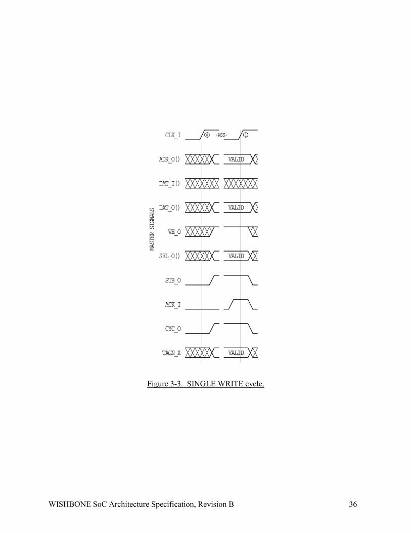
Figure 3-3 shows a SINGLE WRITE cycle. The bus protocol works as follows:
CLOCK EDGE 0: MASTER presents [ADR_O()] and [TAGN_O].MASTER asserts [WE_O] to indicate a WRITE cycle.MASTER presents bank select [SEL_O()] to indicate where it sends data.MASTER asserts [CYC_O] to indicate the start of the cycle.MASTER asserts [STB_O] to qualify [ADR_O()], [SEL_O()] and [WE_O].
SETUP, EDGE 1: SLAVE decides inputs, and responds by asserting [ACK_I].SLAVE presents prepares to latch data on [DAT_O()].SLAVE asserts [ACK_I] in response to [STB_O] to indicate latched data.SLAVE presents [TAGN_O].MASTER monitors [TAGN_I].MASTER monitors [ACK_I], and prepares to terminate the cycle.
Note: SLAVE may insert wait states (-WSS-) before asserting [ACK_I],thereby allowing it to throttle the cycle speed. Any number of wait statesmay be added.
CLOCK EDGE 1: SLAVE latches data on [DAT_O()].MASTER latches [TAGN_I].MASTER negates [STB_O] and [CYC_O] to indicate the end of the cycle.
WISHBONE SoC Architecture Specification, Revision B 36
Figure 3-3. SINGLE WRITE cycle.
CLK_I 10
ADR_O()
DAT_I()
DAT_O()
VALID
-WSS-
WE_O
SEL_O()
STB_O
ACK_I
VALID
MASTER SIGNALS
VALID
CYC_O
TAGN_X VALID

WISHBONE SoC Architecture Specification, Revision B 37
3.3 BLOCK READ / WRITE Cycles
The BLOCK transfer cycles perform multiple data transfers. They are very similar to singleREAD and WRITE cycles, but have a few special modifications to support multiple transfers.
During BLOCK cycles, the interface basically performs SINGLE READ/WRITE cycles as de-scribed above. However, the BLOCK cycles are modified somewhat so that these individual cy-cles are combined together to form a single BLOCK cycle. This function is most useful whenmultiple MASTERs are used on the interconnect. For example, if the SLAVE is a shared (dualport) memory, then an arbiter for that memory can determine when one MASTER is done with itso that another can gain access to the memory.
As shown in Figure 3-4, the [CYC_O] signal is asserted for the duration of a BLOCK cycle.This signal can be used to request permission to access from a shared resource from a local arbi-ter, and hold the access until the end of the current cycle. During each of the data transfers(within the block transfer), the normal handshaking protocol between [STB_O] and [ACK_I] ismaintained.
Figure 3-4. Use of [CYC_O] signal during BLOCK cycles.
It should be noted that the [CYC_O] signal does not necessarily rise and fall at the same time as[STB_O]. [CYC_O] may be asserted at the same time as [CYC_O], or one or more [CLK_I]edges before [CYC_O]. Similarly, [CYC_O] may be negated at the same time as [STB_O], orafter an indeterminate number of clock cycles.
RULE 3.200All MASTER and SLAVE interfaces that support BLOCK cycles MUST conform to the timingrequirements given in sections 3.3.1 and 3.3.2.
PERMISSION 3.50MASTER and SLAVE interfaces MAY be designed so that they do not support the BLOCK cy-cles.
CLK_I
STB_O
ACK_I
CYC_O

WISHBONE SoC Architecture Specification, Revision B 38
3.3.1 BLOCK READ Cycle
Figure 3-5 shows a BLOCK READ cycle. The BLOCK cycle is capable of a data transfer onevery clock cycle. However, this example also shows how the MASTER and the SLAVE canboth throttle the bus transfer rate by inserting wait states. A total of five transfers are shown.After the second transfer the MASTER inserts a wait state. After the fourth transfer the SLAVEinserts a wait state. The cycle is terminated after the fifth transfer. The protocol for this transferworks as follows:
CLOCK EDGE 0: MASTER presents [ADR_O()] and [TAGN_O].MASTER negates [WE_O] to indicate a READ cycle.MASTER presents bank select [SEL_O()] to indicate where it expects data.MASTER asserts [CYC_O] to indicate the start of the cycle.MASTER asserts [STB_O].
Note: the MASTER must assert [CYC_O] and/or [TAGN_O] at, or anytimebefore, clock edge 1. The use of [TAGN_O] is optional.
SETUP, EDGE 1: SLAVE decodes inputs, and responds by asserting [ACK_I].SLAVE presents valid data on [DAT_I].SLAVE presents [TAGN_O].MASTER monitors [TAGN_I].MASTER monitors [ACK_I], and prepares to latch data on [DAT_I()].
CLOCK EDGE 1: MASTER latches data on [DAT_I()].MASTER latches [TAGN_I].MASTER presents new [ADR_O()] and [TAGN_O].MASTER presents new bank select [SEL_O()] to indicate where data is.
SETUP, EDGE 2: SLAVE decodes inputs, and responds by asserting [ACK_I].SLAVE presents valid data on [DAT_I].SLAVE presents [TAGN_O].MASTER monitors [TAGN_I].MASTER monitors [ACK_I], and prepares to latch data on [DAT_I()].
CLOCK EDGE 2: MASTER latches data on [DAT_I()].MASTER latches [TAGN_I].MASTER negates [STB_O] to introduce a wait state (-WSM-).
SETUP, EDGE 3: SLAVE negates [ACK_I] in response to [STB_O].
Note: any number of wait states can be inserted by the MASTER at thispoint.
CLOCK EDGE 3: MASTER presents new [ADR_O()] and [TAGN_O].MASTER presents new bank select [SEL_O()].

WISHBONE SoC Architecture Specification, Revision B 39
MASTER asserts [STB_O].
SETUP, EDGE 4: SLAVE decodes inputs, and responds by asserting [ACK_I].SLAVE presents valid data on [DAT_I].SLAVE presents [TAGN_O].MASTER monitors [TAGN_I].MASTER monitors [ACK_I], and prepares to latch data on [DAT_I()].
CLOCK EDGE 4: MASTER latches data on [DAT_I()].MASTER presents [ADR_O()] and [TAGN_O].MASTER latches [TAGN_I].MASTER presents new bank select [SEL_O()] to indicate where it expectsdata.
SETUP, EDGE 5: SLAVE decodes inputs, and responds by asserting [ACK_I].SLAVE presents valid data on [DAT_I].SLAVE presents [TAGN_O].MASTER monitors [TAGN_I].MASTER monitors [ACK_I], and prepares to latch data on [DAT_I()].
CLOCK EDGE 5: MASTER latches data on [DAT_I()].MASTER latches [TAGN_I].SLAVE negates [ACK_I] to introduce a wait state.
Note: any number of wait states can be inserted by the SLAVE at this point.
SETUP, EDGE 6: SLAVE decodes inputs, and responds by asserting [ACK_I].SLAVE presents valid data on [DAT_I].MASTER monitors [ACK_I], and prepares to latch data on [DAT_I()].
CLOCK EDGE 6: MASTER latches data on [DAT_I()].MASTER terminates cycle by negating [STB_O] and [CYC_O].

WISHBONE SoC Architecture Specification, Revision B 40
Figure 3-5. BLOCK READ cycle.
CLK_I 10
ADR_O()
DAT_I()
DAT_O()
VALID
WE_O
SEL_O()
STB_O
ACK_I
VALID
MASTER SIGNALS
2
VALID
VALID
CYC_O
TAGN_X
3 4-WSM-
VALID
VALID
5
VALID
VALID
VALID VALID
-WSS- 6
VALID
VALID VALID
VALID VALID VALID VALID

WISHBONE SoC Architecture Specification, Revision B 41
3.3.2 BLOCK WRITE Cycle
Figure 3-6 shows a BLOCK WRITE cycle. The BLOCK cycle is capable of a data transfer onevery clock cycle. However, this example also shows how the MASTER and the SLAVE canboth throttle the bus transfer rate by inserting wait states. A total of five transfers are shown.After the second transfer the MASTER inserts a wait state. After the fourth transfer the SLAVEinserts a wait state. The cycle is terminated after the fifth transfer. The protocol for this transferworks as follows:
CLOCK EDGE 0: MASTER presents [ADR_O()] and [TAGN_O].MASTER asserts [WE_O] to indicate a WRITE cycle.MASTER presents bank select [SEL_O()] to indicate where it expects data.MASTER asserts [CYC_O] and [TAGN_O] to indicate cycle start.MASTER asserts [STB_O].
Note: the MASTER must assert [CYC_O] and/or [TAGN_O] at, or anytimebefore, clock edge 1. The use of [TAGN_O] is optional.
SETUP, EDGE 1: SLAVE decodes inputs, and responds by asserting [ACK_I].SLAVE prepares to latch data on [DAT_O].SLAVE presents [TAGN_O].MASTER monitors [TAGN_I].MASTER monitors [ACK_I], and prepares to terminate current data phase.
CLOCK EDGE 1: SLAVE latches data on [DAT_O()].MASTER latches [TAGN_I].MASTER presents [ADR_O()] and [TAGN_O].MASTER presents new bank select [SEL_O()].
SETUP, EDGE 2: SLAVE decodes inputs, and responds by asserting [ACK_I].SLAVE prepares to latch data on [DAT_O].SLAVE presents [TAGN_O].MASTER monitors [TAGN_I].MASTER monitors [ACK_I], and prepares to terminate current data phase.
CLOCK EDGE 2: SLAVE latches data on [DAT_O()].MASTER latches [TAGN_I].MASTER negates [STB_O] to introduce a wait state (-WSM-).
SETUP, EDGE 3: SLAVE negates [ACK_I] in response to [STB_O].
Note: any number of wait states can be inserted by the MASTER at thispoint.
CLOCK EDGE 3: MASTER presents [ADR_O()] and [TAGN_O].MASTER presents bank select [SEL_O()] to indicate where it expects data.

WISHBONE SoC Architecture Specification, Revision B 42
MASTER asserts [STB_O].
SETUP, EDGE 4: SLAVE decodes inputs, and responds by asserting [ACK_I].SLAVE prepares to latch data on [DAT_O].SLAVE presents [TAGN_O].MASTER monitors [TAGN_I].MASTER monitors [ACK_I], and prepares to terminate data phase.
CLOCK EDGE 4: SLAVE latches data on [DAT_O()].MASTER latches [TAGN_I].MASTER presents [ADR_O()] and [TAGN_O].MASTER presents new bank select [SEL_O()] to indicate where it expectsdata.
SETUP, EDGE 5: SLAVE decodes inputs, and responds by asserting [ACK_I].SLAVE prepares to latch data on [DAT_O].SLAVE presents [TAGN_O].MASTER monitors [TAGN_I].MASTER monitors [ACK_I], and prepares to terminate data phase.
CLOCK EDGE 5: SLAVE latches data on [DAT_O()].SLAVE negates [ACK_I] to introduce a wait state.MASTER latches [TAGN_I].
Note: any number of wait states can be inserted by the SLAVE at this point.
SETUP, EDGE 6: SLAVE decodes inputs, and responds by asserting [ACK_I].SLAVE prepares to latch data on [DAT_O].MASTER monitors [ACK_I], and prepares to terminate data phase.
CLOCK EDGE 6: SLAVE latches data on [DAT_O()].MASTER terminates cycle by negating [STB_O] and [CYC_O].

WISHBONE SoC Architecture Specification, Revision B 43
Figure 3-6. BLOCK WRITE cycle.
CLK_I 10
ADR_O()
DAT_I()
DAT_O()
VALID
WE_O
SEL_O()
STB_O
ACK_I
MASTER SIGNALS
2
VALID
CYC_O
TAGN_X
3 4-WSM-
VALID
5
VALID
VALID VALID
-WSS- 6
VALID VALID
VALID VALID VALID VALID
VALID VALID VALID VALID

WISHBONE SoC Architecture Specification, Revision B 44
3.4 RMW Cycle
The RMW (read-modify-write) cycle is used for indivisible semaphore operations. During thefirst half of the cycle a single read data transfer is performed. During the second half of the cyclea write data transfer is performed. The [CYC_O] signal remains asserted during both halves ofthe cycle.
RULE 3.210All MASTER and SLAVE interfaces that support RMW cycles MUST conform to the timingrequirements given in section 3.4.
PERMISSION 3.60MASTER and SLAVE interfaces MAY be designed so that they do not support the RMW cy-cles.
Figure 3-7 shows a read-modify-write (RMW) cycle. The RMW cycle is capable of a data trans-fer on every clock cycle. However, this example also shows how the MASTER and the SLAVEcan both throttle the bus transfer rate by inserting wait states. Two transfers are shown. After thefirst (read) transfer, the MASTER inserts a wait state. During the second transfer the SLAVEinserts a wait state. The protocol for this transfer works as follows:
CLOCK EDGE 0: MASTER presents [ADR_O()] and [TAGN_O].MASTER negates [WE_O] to indicate a READ cycle.MASTER presents bank select [SEL_O()] to indicate where it expects data.MASTER asserts [CYC_O] and [TAGN_O] to indicate the start of cycle.MASTER asserts [STB_O].
Note: the MASTER must assert [CYC_O] and/or [TAGN_O] at, or anytimebefore, clock edge 1. The use of [TAGN_O] is optional.
SETUP, EDGE 1: SLAVE decodes inputs, and responds by asserting [ACK_I].SLAVE presents valid data on [DAT_I].SLAVE presents [TAGN_O].MASTER monitors [TAGN_I].MASTER monitors [ACK_I], and prepares to latch data on [DAT_I()].
CLOCK EDGE 1: MASTER latches data on [DAT_I()].MASTER latches [TAGN_I].MASTER negates [STB_O] to introduce a wait state (-WSM-).
SETUP, EDGE 2: SLAVE negates [ACK_I] in response to [STB_O].MASTER asserts [WE_O] to indicate a WRITE cycle.
Note: any number of wait states can be inserted by the MASTER at thispoint.

WISHBONE SoC Architecture Specification, Revision B 45
CLOCK EDGE 2: MASTER presents the same [ADR_O()] and [TAGN_O] as was on clock 1.MASTER presents WRITE data on [DAT_O()].MASTER presents new bank select [SEL_O()].MASTER asserts [STB_O].
SETUP, EDGE 3: SLAVE decodes inputs, and responds by asserting [ACK_I] (when ready).SLAVE presents valid data on [DAT_I].SLAVE presents [TAGN_O].MASTER monitors [TAGN_I].MASTER monitors [ACK_I], and prepares to latch data on [DAT_I()].
Note: any number of wait states can be inserted by the SLAVE at this point.
CLOCK EDGE 3: SLAVE latches data on [DAT_O()].MASTER latches [TAGN_I].MASTER negates [STB_O] and [CYC_O] indicating the end of the cycle.SLAVE negates [ACK_I] in response to negated [STB_O].

WISHBONE SoC Architecture Specification, Revision B 46
Figure 3-7. RMW cycle.
CLK_I 10
ADR_O()
DAT_I()
DAT_O()
VALID
WE_O
SEL_O()
STB_O
ACK_I
VALID
VALIDMASTER SIGNALS
CYC_O
TAGN_X
-WSM- -WSS-2 3
VALID
VALID
VALID
VALID VALID

WISHBONE SoC Architecture Specification, Revision B 47
3.5 Data Organization
Data organization refers to the ordering of data during transfers. There are two general types ofordering which are called BIG ENDIAN and LITTLE ENDIAN. BIG ENDIAN refers to dataordering where the most significant portion of an operand is stored at the lower address. LIT-TLE ENDIAN refers to data ordering where the most significant portion of an operand is storedat the higher address. The WISHBONE architecture supports both methods of data ordering.
3.5.1 Nomenclature
A BYTE(N), WORD(N), DWORD(N) and QWORD(N) nomenclature is used to define data or-dering. These terms are defined in Table 3-1. Figure 3-8 shows the operand locations for inputand output data ports.
Table 3-1. Data transfer nomenclature.
Data Transfer NomenclatureNomenclature Granularity Description
BYTE(N) 8-bit An 8-bit BYTE transfer at address ‘N’.WORD(N) 16-bit A 16-bit WORD transfer at address ‘N’.
DWORD(N) 32-bit A 32-bit Double WORD transfer at address ‘N’.QWORD(N) 64-bit A 64-bit Quadruple WORD transfer at address ‘N’.
The table also defines the granularity of the interface. This indicates the minimum unit of datatransfer that is supported by the interface. For example, the smallest operand that can be passedthrough a port with 16-bit granularity is a 16-bit WORD. In this case, an 8-bit operand cannot betransferred.
Figure 3-9 shows an example of how the 64-bit value of 0x0123456789ABC is transferredthrough BYTE, WORD, DWORD and QWORD ports using BIG ENDIAN data organization.Through the 64-bit QWORD port the number is directly transferred with the most significant bitat DAT_I / DAT_O(63). The least significant bit is at DAT_I / DAT_O(0). However, when thesame operand is transferred through a 32-bit DWORD port, it is split into two bus cycles. Thetwo bus cycles are each 32-bits in length, with the most significant DWORD transferred at thelower address, and the least significant DWORD transferred at the upper address. A similarsituation applies to the WORD and BYTE cases.
Figure 3-10 shows an example of how the 64-bit value of 0x0123456789ABC is transferredthrough BYTE, WORD, DWORD and QWORD ports using LITTLE ENDIAN data organiza-tion. Through the 64-bit QWORD port the number is directly transferred with the most signifi-cant bit at DAT_I / DAT_O(63). The least significant bit is at DAT_I / DAT_O(0). However,when the same operand is transferred through a 32-bit DWORD port, it is split into two bus cy-cles. The two bus cycles are each 32-bits in length, with the least significant DWORD trans-

WISHBONE SoC Architecture Specification, Revision B 48
ferred at the lower address, and the most significant DWORD transferred at the upper address. Asimilar situation applies to the WORD and BYTE cases.
Figure 3-8. Operand locations for input and output data ports.
BYTE(0)0
1
2
3
4
5
6
7
OFFSETADDRESS
BYTEORDERING
BYTE(1)
BYTE(2)
BYTE(3)
BYTE(4)
BYTE(5)
BYTE(6)
BYTE(7)
WORD(0)
WORD(1)
WORD(2)
WORD(3)
0007
0015
WORDORDERING
0031
DWORDORDERING
DWORD(0)
DWORD(1)
DAT_I / DAT_O
DAT_I / DAT_O
DAT_I / DAT_O
QWORDORDERING
0
00DAT_I / DAT_O63
QWORD(0)
00DAT_I / DAT_O63
00DAT_I / DAT_O63
(a) BIG ENDIAN BYTE, WORD, DWORD and QWORD positioning in a 64-bit operand.
(b) LITTLE ENDIAN BYTE, WORD, DWORD and QWORD positioning in a 64-bit operand.
(c) Address nomenclature.
BYTE(0)
BYTE(0)BYTE(1)
BYTE(1) BYTE(2)
BYTE(2)BYTE(3)
BYTE(3) BYTE(4)
BYTE(4)
BYTE(5)
BYTE(5)BYTE(6)
BYTE(6)
BYTE(7)
BYTE(7)
WORD(0)
WORD(0)WORD(1)
WORD(1)
WORD(2)
WORD(2)
WORD(3)
WORD(3)
DWORD(0)
DWORD(0) DWORD(1)
DWORD(1)
QWORD(0)
QWORD(0)

WISHBONE SoC Architecture Specification, Revision B 49
Figure 3-9. Example showing a variety of BIG ENDIAN transfers over various port sizes.
Figure 3-10. Example showing a variety of LITTLE ENDIAN transfers over various port sizes.
0xEF
0
1
2
3
4
5
6
7
OFFSETADDRESS
BYTEORDERING
0xCD
0xAB
0x89
0x67
0x45
0x23
0x01
0xCDEF
0x89AB
0x4567
0x0123
0007
0015
WORDORDERING
0031
DWORDORDERING
0x89ABCDEF
0x01234567
DAT_I / DAT_O
DAT_I / DAT_O
DAT_I / DAT_O
QWORDORDERING
0
00DAT_I / DAT_O63
0x0123456789ABCDEF
0
1
2
3
4
5
6
7
OFFSETADDRESS
BYTEORDERING
0007
0015
WORDORDERING
0031
DWORDORDERING
DAT_I / DAT_O
DAT_I / DAT_O
DAT_I / DAT_O
QWORDORDERING
0
00DAT_I / DAT_O63
0x0123456789ABCDEF
0x01
0x23
0x45
0x67
0x89
0xAB
0xCD
0xEF
0x0123
0x4567
0x89AB
0xCDEF
0x01234567
0x89ABCDEF

WISHBONE SoC Architecture Specification, Revision B 50
RULE 3.220Data organization MUST conform to the ordering indicated in Figure 3-8.
RULE 3.230The WISHBONE DATASHEET MUST indicate the port size. The port size MUST be indicatedas: 8-bit, 16-bit, 32-bit or 64-bit.
RULE 3.235The WISHBONE DATASHEET MUST indicate the port granularity. The granularity MUST beindicated as: 8-bit, 16-bit, 32-bit or 64-bit.
RULE 3.237The WISHBONE DATASHEET MUST indicate the maximum operand size. The maximumoperand size MUST be indicated as: 8-bit, 16-bit, 32-bit or 64-bit.
PERMISSION 3.35In some cases the maximum operand size is unknown. In those cases, the maximum operandsize shall be the same as the granularity.
RULE 3.240The WISHBONE DATASHEET MUST indicate the data transfer ordering. The ordering MUSTbe indicated as BIG ENDIAN or LITTLE ENDIAN.
PERMISSION 3.70When the port size equals the granularity, then the interface may be specified as BIG ENDIANand/or LITTLE ENDIAN.
OBSERVATION 3.40When the port size equals the granularity, then BIG ENDIAN and LITTLE ENDIAN transfersare identical.
3.5.2 Transfer Sequencing
The sequence in which data is transferred through a port is not regulated by this specification.For example, a 64-bit operand through a 32-bit port will take two bus cycles. However, thespecification does not require that the lower or upper DWORD be transferred first.
RECOMMENDATION 3.05Design interfaces so that data is transferred sequentially from lower addresses to a higher ad-dresses.
OBSERVATION 3.50The sequence in which an operand is transferred through a data port is not highly regulated bythe specification. That is because different IP cores may produce the data in different ways. Thesequence is therefore application-specific.

WISHBONE SoC Architecture Specification, Revision B 51
RULE 2.45The WISHBONE DATASHEET MUST indicate the sequence of data transfer through the port.If the sequence of data transfer is not known, then the datasheet MUST indicate that it is unde-fined.
3.5.3 Data Organization for 64-bit Ports
RULE 3.250Data organization on 64-bit ports MUST conform to Figure 3-11.
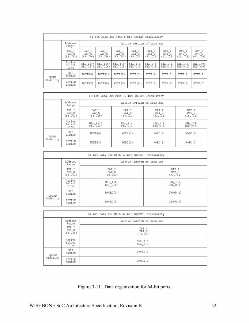
WISHBONE SoC Architecture Specification, Revision B 52
Figure 3-11. Data organization for 64-bit ports.
BYTE(7)
DAT_IDAT_O
(07..00)
SEL_I(0)SEL_O(0)
BYTE(6)
BYTE(5)BYTE(4)BYTE(3)BYTE(2)BYTE(1)BYTE(0)
ADR_IADR_O
(63..03)
DAT_IDAT_O
(15..08)
DAT_IDAT_O
(23..16)
DAT_IDAT_O
(31..24)
DAT_IDAT_O
(39..32)
DAT_IDAT_O
(47..40)
DAT_IDAT_O
(55..48)
DAT_IDAT_O
(63..56)
SEL_I(1)SEL_O(1)
SEL_I(2)SEL_O(2)
SEL_I(3)SEL_O(3)
SEL_I(4)SEL_O(4)
SEL_I(5)SEL_O(5)
SEL_I(6)SEL_O(6)
SEL_I(7)SEL_O(7)
Active Portion of Data BusAddressRange:
LITTLEENDIAN
BYTEOrdering
ActiveSelectLine
64-bit Data Bus With 8-bit (BYTE) Granularity
WORD(3)
DAT_IDAT_O
(15..00)
SEL_I(0)SEL_O(0)
WORD(2)WORD(1)WORD(0)
ADR_IADR_O
(63..02)
DAT_IDAT_O
(31..16)
DAT_IDAT_O
(47..32)
DAT_IDAT_O
(63..48)
SEL_I(1)SEL_O(1)
SEL_I(2)SEL_O(2)
SEL_I(3)SEL_O(3)
Active Portion of Data BusAddressRange
ActiveSelectLine
64-bit Data Bus With 16-bit (WORD) Granularity
DWORD(1)
DAT_IDAT_O
(31..00)
SEL_I(0)SEL_O(0)
DWORD(0)
ADR_IADR_O
(63..01)
DAT_IDAT_O
(63..32)
SEL_I(1)SEL_O(1)
DWORD(1) DWORD(0)
Active Portion of Data BusAddressRange
ActiveSelectLine
64-bit Data Bus With 32-bit (DWORD) Granularity
QWORD(0)
DAT_IDAT_O
(63..00)
SEL_I(0)SEL_O(0)
ADR_IADR_O
(63..00)
QWORD(0)
Active Portion of Data BusAddressRange
ActiveSelectLine
64-bit Data Bus With 64-bit (QWORD) Granularity
BIGENDIAN BYTE(6)
BYTE(7) BYTE(5) BYTE(4) BYTE(3) BYTE(2) BYTE(1) BYTE(0)
WORDOrdering
BIGENDIAN
LITTLEENDIAN WORD(0)WORD(1)WORD(2)WORD(3)
BIGENDIAN
LITTLEENDIAN
DWORDOrdering
QWORDOrdering
BIGENDIAN
LITTLEENDIAN

WISHBONE SoC Architecture Specification, Revision B 53
3.5.4 Data Organization for 32-bit Ports
RULE 3.260Data organization on 32-bit ports MUST conform to Figure 3-12.
Figure 3-12. Data organization for 32-bit ports.
BYTE(3)BYTE(7)
DAT_IDAT_O
(07..00)
SEL_I(0)SEL_O(0)
BYTE(2)BYTE(6)
BYTE(1)BYTE(5)
BYTE(0)BYTE(4)
ADR_IADR_O
(63..02)
DAT_IDAT_O
(15..08)
DAT_IDAT_O
(23..16)
DAT_IDAT_O
(31..24)
SEL_I(1)SEL_O(1)
SEL_I(2)SEL_O(2)
SEL_I(3)SEL_O(3)
Active Portion of Data BusAddressRange
LITTLEENDIAN
BIGENDIAN
ActiveSelectLine
32-bit Data Bus With 8-bit (BYTE) Granularity
WORD(1)WORD(3)
DAT_IDAT_O
(15..00)
SEL_I(0)SEL_O(0)
WORD(0)WORD(2)
ADR_IADR_O
(63..01)
DAT_IDAT_O
(31..16)
SEL_I(1)SEL_O(1)
Active Portion of Data BusAddressRange
ActiveSelectLine
32-bit Data Bus With 16-bit (WORD) Granularity
DWORD(0)DWORD(1)
DAT_IDAT_O
(31..00)
SEL_I(0)SEL_O(0)
ADR_IADR_O
(63..00)
Active Portion of Data BusAddressRange
ActiveSelectLine
32-bit Data Bus With 32-bit (DWORD) Granularity
BIGENDIAN
LITTLEENDIAN
BIGENDIAN
LITTLEENDIAN
BYTEOrdering
WORDOrdering
DWORDOrdering
BYTE(3)BYTE(7)
BYTE(2)BYTE(6)
BYTE(1)BYTE(5)
BYTE(0)BYTE(4)
WORD(0)WORD(2)
WORD(1)WORD(3)
DWORD(0)DWORD(1)

WISHBONE SoC Architecture Specification, Revision B 54
3.5.5 Data Organization for 16-bit Ports
RULE 3.270Data organization on 16-bit ports MUST conform to Figure 3-13.
Figure 3-13. Data organization for 16-bit ports.
DAT_IDAT_O
(07..00)
SEL_I(0)SEL_O(0)
BYTE(0)BYTE(2)BYTE(4)BYTE(6)
ADR_IADR_O
(63..01)
DAT_IDAT_O
(15..08)
SEL_I(1)SEL_O(1)
Active Portionof Data BusAddress
Range
LITTLEENDIAN
BIGENDIAN
ActiveSelectLine
16-bit Data Bus With8-bit (BYTE) Granularity
DAT_IDAT_O
(15..00)
SEL_I(0)SEL_O(0)
ADR_IADR_O
(63..00)
Active Portionof Data BusAddress
Range
ActiveSelectLine
16-bit Data Bus With16-bit (WORD) Granularity
WORD(0)WORD(1)WORD(2)WORD(3)
BYTEOrdering
WORDOrdering
BIGENDIAN
LITTLEENDIAN
BYTE(1)BYTE(3)BYTE(5)BYTE(7)
BYTE(0)BYTE(2)BYTE(4)BYTE(6)
BYTE(1)BYTE(3)BYTE(5)BYTE(7)
WORD(0)WORD(1)WORD(2)WORD(3)

WISHBONE SoC Architecture Specification, Revision B 55
3.5.6 Data Organization for 8-bit Ports
RULE 3.280Data organization on 8-bit ports MUST conform to Figure 3-14.
Figure 3-14. Data organization for 8-bit ports.
BYTE(0)BYTE(1)BYTE(2)BYTE(3)BYTE(4)BYTE(5)BYTE(6)BYTE(7)
DAT_IDAT_O
(07..00)
SEL_I(0)SEL_O(0)
ADR_IADR_O
(63..00)
ActivePortion
ofData Bus
AddressRange
BYTEOrdering
BIGENDIAN
ActiveSelectLine
8-bit Data Bus With8-bit (BYTE) Granularity
BYTE(0)BYTE(1)BYTE(2)BYTE(3)BYTE(4)BYTE(5)BYTE(6)BYTE(7)
LITTLEENDIAN

WISHBONE SoC Architecture Specification, Revision B 56
Chapter 4 – Timing Specification
The WISHBONE specification is designed to provide the end user with very simple timing con-straints. Although the application specific circuit(s) will vary in this regard, the interface itself isdesigned to work without the need for detailed timing specifications. In all cases, the only tim-ing information that is needed by the end user is the maximum clock frequency (for [CLK_I])that is passed to a place & route tool. The maximum clock frequency is dictated by the time de-lay between a positive clock edge on [CLK_I] to the setup on a stage further down the logicalsignal path. This delay is shown graphically in Figure 4-1, and is defined as Tpd,clk-su.
Figure 4-1. Definition for Tpd,clk-su.
RULE 4.10The clock input [CLK_I] to each IP core MUST coordinate all activities for the internal logicwithin the WISHBONE interface. All WISHBONE output signals are registered at the risingedge of [CLK_I]. All WISHBONE input signals must be stable before the rising edge of[CLK_I].
PERMISSION 4.10The user’s place and route tool MAY be used to enforce this rule.
OBSERVATION 4.10Most place and route tools can be easily configured to enforce this rule. Generally, it only re-quires a single timing specification for Tpd,clk-su.
RULE 4.20The WISHBONE interface MUST use synchronous, RTL design methodologies that, givennearly infinitely fast gate delays, will operate over a nearly infinite range of clock frequencies on[CLK_I].
CLK_I
D Q
CE
D Q
Tpd,clk-su = 1/Fclk
INTERCONNECTIONLOGIC & ROUTE DELAY
SIGNAL

WISHBONE SoC Architecture Specification, Revision B 57
OBSERVATION 4.20Realistically, the WISHBONE interface will never be expected to operate over a nearly infinitefrequency range. However this requirement eliminates the need for non-portable timing con-straints (that may work only on certain target devices).
OBSERVATION 4.30The WISHBONE interface logic assumes that a low-skew clock distribution scheme is used onthe target device, and that the clock-skew shall be low enough to permit reliable operation overthe environmental conditions.
PERMISSION 4.20The IP core connected to a WISHBONE interface MAY include application specific timing re-quirements.
RULE 4.30The clock input [CLK_I] MUST have a duty cycle that is no less than 40%, and no greater than60%.
SUGGESTION 4.1Design an IP core so that all of the circuits (including the WISHBONE interconnect) follow theaforementioned RULEs, as this will make the core portable across a wide range of target devicesand technologies.
RULE 4.40The WISHBONE DATASHEET MUST indicate if the SoC component has any constraints on its[CLK_I] or [CLK_O] signal.

WISHBONE SoC Architecture Specification, Revision B 58
Chapter 5 – Application Interface
This chapter describes various methods and issues for WISHBONE interconnection. In somecases, the interconnection requires no glue logic. In more sophisticated systems, the user mayneed to add this logic. However, the common interface between the system-on-chip componentswill make this task much simpler.
5.1 Interconnection Methods
There are four general ways to interconnect MASTER and SLAVE IP cores. These include:
• Single MASTER / Single SLAVE interconnection• Single MASTER / Multiple SLAVE interconnection• Multiple MASTER interconnection• Crossbar interconnection
5.1.1 Single MASTER / Single SLAVE Interconnection
The application interface may be operated with a single MASTER and a single SLAVE. Thisinterconnection is generally the simplest and the fastest way to integrate IP cores. It is simplestbecause (in many cases) the MASTER and SLAVE can simply be connected together. Figure 5-1 shows an example of this interconnection. It should be noted that this example assumes thatthe port widths, port granularities, operand sizes and address widths are equal.
5.1.2 Single MASTER / Multiple SLAVE Interconnection
The WISHBONE application interface may be operated with a single MASTER and multipleSLAVEs. Refer to the multiple MASTER configuration (below) for more information.
5.1.3 Multiple MASTER Interconnection
The WISHBONE application interface may be operated with multiple MASTER interconnec-tions. Figure 5-2 shows a sample application interface with two WISHBONE MASTERs, andtwo WISHBONE SLAVEs. For purposes of clarity, only the [CYC_O], [STB_O] and [ACK_I]signals are shown. Figure 5-3 shows a sample timing diagram for the same circuit.
At the beginning of a bus cycle a MASTER asserts its [CYC_O] signal. The [CYC_O] signalsfrom the two MASTERs are routed to an arbiter that determines which gets possession of the in-terconnection. The winning MASTER is identified by the arbiter by the assertion of [GNT1] or[GNT2], which correspond to the first and second masters respectively. The grant signals are

WISHBONE SoC Architecture Specification, Revision B 59
then used determine which of the MASTERs will drive the common cycle [COMCYC] andstrobe [COMSTB] signals.
The acknowledge signals from the SLAVEs are ‘or’ed together to form a common acknowledgesignal [COMACK]. In this case, each slave will decode the common address (not shown), andwill respond if it is the participating slave in a bus cycle.
The other interconnect signals (e.g. [DAT_I] and [DAT_O]) are not shown in this example.These can be interconnected using multiplexors or three-state buses.
Figure 5-1. Single MASTER / Single SLAVE interconnection example.
5.1.4 Crossbar Interconnection
The WISHBONE MASTERs and SLAVEs may be interconnected with a crossbar switch.Crossbar switches are systems that usually have multiple MASTERs and multiple SLAVEs.
Crossbar switches are mechanisms that allow individual pairs of MASTERs and SLAVEs toconnect and communicate. Each connection channel can be operated in parallel to other connec-tion channels. This increases the data transfer rate of the entire system by employing parallel-ism. Stated another way, two 100 Mbyte/second channels can operate in parallel, thereby pro-viding a 200 Mbyte/second transfer rate. This makes the crossbar switches inherently faster thantraditional bus schemes.
Crossbar routing mechanisms generally support dynamic configurability. This essentially cre-ates a reconfigurable and reliable network system. Most crossbar architectures are also scalable,meaning that families of crossbars can be added as the needs arise.
CLK_IADR_O()DAT_I()
DAT_O()WE_O
SEL_O()STB_OACK_I
CLK_IADR_I()DAT_I()
DAT_O()WE_ISEL_I()STB_IACK_O
WISHBONE MASTER
WISHBONE SLAVE
CYC_O CYC_ITAGN_O TAGN_I
RST_I RST_I
TAGN_I TAGN_OUSER
DEFINED

WISHBONE SoC Architecture Specification, Revision B 60
Figure 5-2. Sample application with two WISHBONE MASTERs,and two WISHBONE SLAVEs.
STB_O
ACK_IWISHBONE
MASTER #1
CYC_O
ARBITER
CYC1CYC2
GNT1GNT2
COMSTB
COMCYC
STB_O
ACK_I
WISHBONE
MASTER #2
CYC_O
STB_I
ACK_O
WISHBONE
SLAVE #1
CYC_I
STB_I
ACK_O
WISHBONE
SLAVE #2
CYC_I
APPLICATION INTERFACE
01
00
10
11UNUSEDSTATE
STATES: GNT2, GNT1INPUTS: RST_I, CYC2, CYC1
XXX
1XX
0X1
010
01X
0X1
000
000
000 001 010
ARBITER STATE DIAGRAM
ARBITER EQUATIONS:
GNT1 <= ( not(RST_I) and not(GNT2) and CYC1 ) or ( not(RST_I) and not(GNT1) and not(CYC2) and CYC1 );
GNT2 <= ( not(RST_I) and not(GNT2) and CYC2 and not(CYC1) ) or ( not(RST_I) and GNT2 and not(GNT1) and CYC2 );
COMACK

WISHBONE SoC Architecture Specification, Revision B 61
Figure 5-3. Timing diagram for multiple MASTER / multiple SLAVE example.
5.2 Three-State Interconnections
The interconnection can take the form of a three-state bus. Figure 5-4 shows the connection of aMASTER or SLAVE data input and output buses to a three-state data bus. Also note that theresistor/current source listed in the figure can also be a ‘pull-down’ resistor or current source.
Figure 5-4. Connection of data bus to a three-state interconnection.
CLK_I 10
CYC1
CYC2
GNT1
GNT2
2 3 4 5
COMCYC
6 7
COMSTB
COMACK
THREE-STATEBUFFER
DAT_IO(0)
THREE-STATEINTERCONNECT
CLK_I
D Q
CE
Q D
CE
DAT_O(0)
DAT_I(0)
Vcc
RESISTOR-OR-
CURRENTSOURCE
SIGNALNAME
TRANSLATION
THREE-STATE CONTROL

WISHBONE SoC Architecture Specification, Revision B 62
5.3 Endian Conversion
In some cases the user may wish to connect a BIG ENDIAN IP core to a LITTLE ENDIAN IPcore. In many cases the conversion is quite straightforward, and does not require any exoticconversion logic. Furthermore, the conversion does not create any speed degradation of the in-terface. In general, the ENDIAN conversion takes place by renaming the data and select I/O sig-nals at the source or destination IP core.
Figure 5-5 shows a simple example where a 32-bit BIG ENDIAN core output (CORE ‘A’) isconnected to a 32-bit LITTLE ENDIAN core input (CORE ‘B’). Both cores have 32-bit operandsizes and 8-bit granularity. As can be seen in the diagram, the ENDIAN conversion is accom-plished by cross coupling the data and select signal arrays. This is quite simple since the conver-sion is accomplished by the interconnection wiring between the cores. This is especially simplein soft IP cores (using VHDL or Verilog hardware description languages), as it only requiresthe renaming of signals.
In some cases the address lines may also need to be modified between the two cores. For exam-ple, if 64-bit operands are transferred between two cores with 8-bit port sizes, then the addresslines may need to be modified as well.
Figure 5-5. Converting a BIG ENDIAN output to a LITTLE ENDIAN input.
DAT_O(07..00) DAT_I(07..00)
CORE 'B'(Input)
LITTLE ENDIAN
CORE 'A'(Output)BIG ENDIAN
DAT_O(15..08)
DAT_O(23..16)
DAT_O(31..24)
DAT_I(15..08)
DAT_I(23..16)
DAT_I(31..24)
SEL_O(2)
SEL_O(3)
SEL_O(1)
SEL_O(0)
SEL_I(3)
SEL_I(2)
SEL_I(1)
SEL_I(0)

WISHBONE SoC Architecture Specification, Revision B 63
References
[1] Cohen, Danny. On Holy Wars and a Plea for Peace. IEEE Computer Magazine, October1981. Pages 49-54. [Description of BIG ENDIAN and LITTLE ENDIAN.]

WISHBONE SoC Architecture Specification, Revision B 64
Appendix A – WISHBONE Design Philosophy(This appendix is not part of the WISHBONE specification).
The design philosophy behind the WISHBONE system-on-chip (SoC) architecture is very simi-lar to that found in standard microcomputer buses like PCI and VMEbus. However, there aresome important differences between these two approaches. This application note describes someof the fundamental characteristics of the WISHBONE SoC architecture by comparing and con-trasting it to standard bus technologies.
This method for describing WISHBONE is useful because SoC often requires new ways ofthinking about microcomputer bus architectures. For the most part, SoC integration is no differ-ent than traditional approaches. However, the design strategies on SoC can be radically differentbecause they are integrated on a single semiconductor device. This is especially true if the SoCinterconnection takes full advantage of the technology.
This application note is also useful if the reader is approaching SoC from a background of tradi-tional microcomputer buses like PCI or VMEbus. In this case the reader may find that tradi-tional concepts, such as three-state buses and fixed timing requirements, are not required in SoCarchitectures like WISHBONE. In some cases, the reader may discover that he or she must learna ‘new way of thinking’ about the microcomputer bus problem
This application note attempts to:
• Identify the important differences between standard and SoC bus architectures.
• Discuss where (and why) multiplexed address and data paths are used.
• Discuss where (and why) three-state interconnections are used.
• Discuss the difference between fixed and variable interconnection systems.
• Describe the methodologies for creating timing parameters.
• Present some of the design trade-offs between standard and SoC architectures.
• Discuss testability issues.
• Present some of the solutions afforded by the WISHBONE SoC architecture.
General Differences in Design Philosophies
There are several distinctions between standard and SoC bus architectures. These include:

WISHBONE SoC Architecture Specification, Revision B 65
• Standard microcomputer buses are always ‘pin limited’, both in terms of connector and ICpackage pins. This often requires strategies such as three-state logic and multiplexed ad-dress and data lines. For the most part, these requirements do not exist on SoC buses likeWISHBONE because they contain a rich set of interconnection (i.e. routing) resources.
• Standard microcomputer buses use a fixed interconnection scheme. That’s because theyare usually routed across a standard backplane. This requirement does not exist on SoCbuses like WISHBONE because it is very easy to change the interconnection resources.This allows a variable interconnection scheme which can support parallel, crossbar switchand other bus structures.
• Standard microcomputer bus slaves fully decode a fixed address. This requirement doesnot exist in SoC buses like WISHBONE because the system integrator has the ability tocreate address decoders that are tailored to his or her application. This reduces redundantlogic and also speeds up the system.
• Standard microcomputer buses have fixed timing requirements. That’s because they areboth tested as sub-assemblies, and have highly capacitive and inductive loads. Further-more, they are designed for the worst-case operating conditions when unknown bus mod-ules are connected together. SoC buses like WISHBONE also have timing requirements,but they are defined so that they can be adjusted by the system integrator for best perform-ance. This is accomplished with a variable timing specification that can be enforced withplace & route tools.
• Standard microcomputer bus modules are tested at the card level. That’s because each busmodule is designed and tested independently. SoC buses like WISHBONE require a higherlevel of testability because they are tested as a system. This problem is somewhat simpli-fied by the fact that they are interconnected at the more abstract ‘tool’ level. The intercon-nections can be described either by source code (like VHDL or Verilog hardware de-scription languages), or with physical layout tools. Both of these solutions require a com-patible set of development tools.
The Pin-limited Design Approach
Standard microcomputer buses like PCI and VMEbus are generally constrained by the number ofconnector and IC package pins that are available. This constraint leads to two design method-ologies:
• Multiplexed address and data buses• Three-state I/O buffers.

WISHBONE SoC Architecture Specification, Revision B 66
Multiplexed Address and Data Buses
Multiplexed address and data buses reduce pin count by routing different types of signals overthe same set of pins. Figure A-1 shows a common technique where address and data lines sharea common set of pins. In this case, a 32-bit address and 32-bit data bus can be combined to forma 32-bit common address/data bus. This reduces the number of signal pins from 64 to 32.
Figure A-1. Circuit and timing diagram for a multiplexed address/data bus.
The major disadvantage of this topology is that it takes twice as long to move the information.Non-multiplexed, synchronous buses can generally move address and data information in as littleas one clock cycle. Multiplexed address and data buses require at least two clock cycles to movethe same information.
The WISHBONE SoC architecture uses non-multiplexed schemes.
Three-State I/O vs. Multiplexor Logic
Three-state I/O buffers can also be used to reduce the number of pins required on the interface,and have long been used in the microcomputer board industry. For example, in master-slave ar-chitectures, the master that ‘owns’ the microcomputer bus turns its buffers ‘on’, and the othermaster(s) turn their buffers ‘off’. [Here, ‘on’ and ‘off’ refer to the three-state and non three-stateconditions, respectively]. This prevents more than one bus master from driving any signal line atany given time. A similar situation also occurs at the slave end. There, the slave enables its out-put buffers during read cycles when it has been selected.
Three-state buffers are sometimes called Tri-State buffers. Tri-State is a registered trademarkof National Semiconductor Corporation.
10
ADD/DATSELECT
DATAADDRESS
ADDRESS DATA
CLOCK
ADD/DATSELECT
OUTPUT
OUTPUT

WISHBONE SoC Architecture Specification, Revision B 67
A simple system that uses three-state I/O buffers is shown in the block diagram of Figure A-2(a).There, the data buses on two master and two slave modules are interconnected with three-statelogic. This situation is required in standard microcomputer buses because there generally aren’tenough IC package or connector pins to do it any other way.
Figure A-2. Three-state bus interconnection vs. multiplexor logic interconnection.
This approach can also be used in the SoC buses. However, the three-state I/O interconnectionshave two major drawbacks. First, they are inherently slower than direct interconnections (be-cause there are always minimum timing parameters that must be met to turn buffers on-and-off).Second, many IC devices do not have three-state internal routing resources available to them, orthey are very restrictive in terms of location or quantity of interconnects.
As shown in Figure A-2(b), the SoC internal bus can use multiplexor logic interconnection toachieve the same goal. The main advantage of this approach is that it does not require the lim-ited three-state routing resources which are available on FPGA and ASIC devices.
10
MASTER #2
DATA OUT
DATA IN
MASTER #1
SLAVE #2
SLAVE #1
10
CNTL 'A'
CNTL 'B'
DATA IN
DATA OUT
DATA OUT
DATA OUT
DATA IN
DATA IN
MASTER #2
DATA IN/OUT
MASTER #2
DATA IN/OUT
SLAVE #1
DATA IN/OUT
SLAVE #2
DATA IN/OUT
(B) MULTIPLEXOR LOGIC INTERCONNECTION
(A) THREE-STATE BUS INTERCONNECTION

WISHBONE SoC Architecture Specification, Revision B 68
The main disadvantage of the multiplexor logic interconnection is that it requires a larger numberof routed interconnects and multiplexor logic (which is not required with the three-state bus ap-proach).
However, there is also a growing body of evidence that suggests that this type of interconnectionis easier to route in FPGA and ASIC devices. Although this is very difficult to quantify, theauthor has found that the multiplexor logic interconnection is quite easily handled by standardFPGA and ASIC routers. This is because:
• Three-state interconnections force place & route software to organize the SoC around thefixed three-state bus locations. In many cases, this constraint results in poorly optimizedand/or slow circuits.
• Very often, ‘bit locations’ within a design are grouped together. In many applications, themultiplexor logic interconnection is easier to handle for place & route tools.
• Pre-defined, external I/O pin locations are easier to achieve with multiplexor logic inter-connections.
WISHBONE supports both three-state and multiplexed interconnections. IP cores with WISH-BONE interfaces use unidirectional ‘in’ and ‘out’ signals, which can easily be converted tothree-state I/O by the system integrator. This is because (as we’ll see shortly) WISHBONE usesa variable interconnection methodology that allows either approach to be used.
Interconnection (Routing) Resources
System-on-chip (SoC) architectures have a rich set of interconnections available to them. Theseare sometimes called routing resources. That’s because they don’t have the connector pin limi-tations that exists on standard microcomputer bus architectures. For this reason, the SoC ap-proach does not require multiplexed address and data buses, nor three-state I/O buffers.
It can be argued that this approach requires more routing resources in the FPGA and ASIC de-vice. However, practical experience has shown that this is not a serious problem. Furthermore,this approach fosters portability of IP cores. This is because the SoC can be configured over agreater range of FPGA and ASIC target devices.
Fixed vs. Variable Interconnections
Standard microcomputer buses like PCI and VMEbus use fixed interconnection resources.These generally take the form of connector pin assignments and their related bus cycles andtiming parameters. To insure that all bus modules are compatible with each other, the intercon-nection resource is fixed (on the backplane). The end user cannot change how the bus modulesare interconnected.

WISHBONE SoC Architecture Specification, Revision B 69
SoC buses like WISHBONE can use variable interconnection methods. This is because the in-terconnection bus is defined by the system integrator at the ‘tool level’. For example, if the SoCis described with a hardware description language like VHDL or Verilog, then the end user hasthe ability to define the interconnection.
For example, Figure A-3 shows two ways that IP cores can be interconnected. In Figure A-3(a)they are interconnected by a shared bus. This is a typical configuration that one might find instandard buses like PCI or VMEbus. In this configuration each master module arbitrates for thecommon, shared bus and then communicate with a slave.
Figure A-3(b) shows a radically different approach. This configuration uses a crossbar switchmatrix. This is a typical configuration that one might find in microcomputer buses like4 RACE-way, SKY Channel or Myrinet.
Under this method, each master arbitrates for a ‘channel’ on the switch. Once this is established,data is transferred between the master and the slave over a private communication link. TheFigure shows two possible channels that may appear on the switch. The first connects master‘MA’ to slave ‘SB’. The second connects master ‘MB’ to slave ‘SA’.
The main advantage of the crossbar switch is that multiple communication paths can operate atthe same time. This means that the overall data transfer rate of the system is increased dramati-cally over the shared bus mechanism. For example, a single communication channel may sup-port 100 Mbyte/sec. However, two parallel communication channels operating simultaneouslywould support 200 Mbyte/sec. This scheme can be expanded dramatically to support extremelyhigh data transfer rates.
4 Raceway: ANSI/VITA 5-1994. SKYchannel: ANSI/VITA 10-1995. Myrinet: ANSI/VITA 26-1998. For moreinformation about these standards see http://www.vita.com.

WISHBONE SoC Architecture Specification, Revision B 70
Figure A-3. Two possible methods for IP core interconnection.
A good analogy of the shared and crossbar switch mechanisms can be drawn from a telephonesystem. The shared bus architecture is much like a ‘party line’ telephone system, where multiplehomes or offices share a single telephone wire. In these systems, only one conversation can hap-pen at any given time.
The crossbar switch operates much like a modern telephone system, where a ‘dialing’ party canconnect to a telephone anywhere else on the system, and over a private communication path.Many such conversations can happen at the same time.
MASTER(IP CORE)
'MA'
MASTER(IP CORE)
'MB'
SLAVE(IP CORE)
'SA'
SLAVE(IP CORE)
'SB'
SLAVE(IP CORE)
'SC'
MASTER(IP CORE)
'MA'
MASTER(IP CORE)
'MB'
SLAVE(IP CORE)
'SA'
SLAVE(IP CORE)
'SB'
SLAVE(IP CORE)
'SC'
CROSSBARSWITCH
(B) CROSSBAR SWITCH INTERCONNECTION.
(A) SHARED BUS INTERCONNECTION.
SHARED BUS
NOTE: DOTTED LINESINDICATE ONE POSSIBLE
CONNECTION OPTION

WISHBONE SoC Architecture Specification, Revision B 71
The variable interconnection scheme can support a plethora of other options as well. For exam-ple, earlier it was discussed how the interconnection could take the form of a three-state or mul-tiplexor logic interconnection. This choice depends upon the end application and the users’ de-sign philosophy.
The variable interconnection scheme also dictates where and how the interconnection bus isspecified. Stated another way, the specification determines where to put the ‘zippers’ in the de-sign. In the case of WISHBONE, the ‘zippers’ are placed at the IP core interface. The intercon-nection scheme itself is not inherently part of the specification.
Full vs. Partial Address Decoding
Standard microcomputer buses like PCI and VMEbus use full address decoding on slave mod-ules. Under that method, each slave module decodes the full address bus. For example, if a 32-bit address bus is used, then each slave decodes all thirty-two address bits.
SoC buses like WISHBONE can use partial address decoding on slave modules. Under thismethod, each slave decodes only the range of addresses that it uses. For example, if the slavehas only four registers, then the WISHBONE interface uses only two address bits. This tech-nique has the following advantages:
• It facilitates high speed address decoders.• It uses less redundant address decoding logic (i.e. fewer gates).• It supports variable address sizing (between zero and 64-bits).• It supports the variable interconnection scheme.
For example, consider the serial I/O port (IP core) with the internal register set shown in FigureA-4(a). If full address decoding is used, then the IP core must include an address decoder to se-lect the module. In this case, the decoder requires: 32 bits – 2 bits = 30 bits. In addition, the IPcore would also contain logic to decode the lower two bits which are used to determine whichI/O registers are selected.
If partial address decoding is used, then the IP core need only decode the two lower address bits(22 = 4). The upper thirty bits are decoded by logic outside of the IP core. In this case the de-coder logic is shown in Figure A-4(b).
Standard microcomputer buses usually use the full address decoding technique. That’s becausethe interconnection method does not allow the creation of any new signals on the interface.However, in SoC buses this limitation does not exist. SoC buses allow the system integrator tomodify the interconnection logic and signal paths.
One advantage of the partial address decoding technique is that the size of the address decoder(on the IP core) is minimized. This speeds up the interface, as decoder logic can be relatively
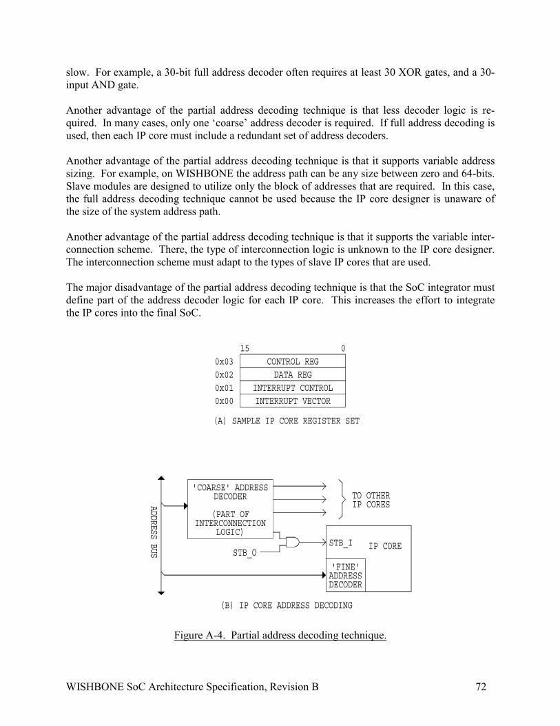
WISHBONE SoC Architecture Specification, Revision B 72
slow. For example, a 30-bit full address decoder often requires at least 30 XOR gates, and a 30-input AND gate.
Another advantage of the partial address decoding technique is that less decoder logic is re-quired. In many cases, only one ‘coarse’ address decoder is required. If full address decoding isused, then each IP core must include a redundant set of address decoders.
Another advantage of the partial address decoding technique is that it supports variable addresssizing. For example, on WISHBONE the address path can be any size between zero and 64-bits.Slave modules are designed to utilize only the block of addresses that are required. In this case,the full address decoding technique cannot be used because the IP core designer is unaware ofthe size of the system address path.
Another advantage of the partial address decoding technique is that it supports the variable inter-connection scheme. There, the type of interconnection logic is unknown to the IP core designer.The interconnection scheme must adapt to the types of slave IP cores that are used.
The major disadvantage of the partial address decoding technique is that the SoC integrator mustdefine part of the address decoder logic for each IP core. This increases the effort to integratethe IP cores into the final SoC.
Figure A-4. Partial address decoding technique.
ADDRESS BUS
'COARSE' ADDRESSDECODER
(PART OFINTERCONNECTION
LOGIC)
IP CORE
'FINE'ADDRESSDECODER
TO OTHERIP CORES
STB_OSTB_I
CONTROL REGDATA REG
INTERRUPT CONTROLINTERRUPT VECTOR
015
0x000x010x020x03
(A) SAMPLE IP CORE REGISTER SET
(B) IP CORE ADDRESS DECODING

WISHBONE SoC Architecture Specification, Revision B 73
Timing Specifications
Standard microcomputer buses like PCI or VMEbus use a fixed timing specification. Under thatmethod, the exact timing requirements are rigidly enforced by the bus specification.
SoC buses like WISHBONE can use a variable timing specification. That means that there areno pre-defined (fixed) timing parameters used on the interconnection. The advantages of thistechnique are:
• Very simple timing constraints can be enforced with place-and-route tools.• The SoC integrator can specify the timing requirements of the system.• The theoretical maximum speed of the system is unlimited.• The maximum speed is limited only by the target device technology.
The WISHBONE SoC architecture assumes that all logic between the IP cores use an RTL(Register Transfer Logic) design approach. Each RTL section assumes the general configurationshown in Figure A-5. This allows a simple and straightforward set of timing rules to be used. Inthe case of WISHBONE, the only timing information that is needed is the maximum clock fre-quency (for [CLK_I]) that is passed to a place & route tool. The maximum clock frequency isdictated by the time delay between a positive clock edge on [CLK_I] to the setup on a stage fur-ther down the logical signal path. This delay is defined as Tpd,clk-su.
Figure A-5. Definition for Tpd,clk-su.
The WISHBONE specification also requires that the following conditions must be met by all ofthe IP cores and interconnection logic:
• A central clock [CLK_I] coordinates all activity on the interconnection.• All output signals are registered at the rising edge of [CLK_I].• All input signals must be stable before the rising edge of [CLK_I].• The central clock [CLK_I] must be distributed on a low-skew interconnection.
If these general guidelines are followed, then the variable timing specification can be used.
CLK_I
D Q
CE
D Q
Tpd,clk-su = 1/Fclk
INTERCONNECTIONLOGIC & ROUTE DELAY
SIGNAL

WISHBONE SoC Architecture Specification, Revision B 74
One advantage to this technique is that very sophisticated systems can be created with only asingle timing specification. In the case of WISHBONE, only ‘Tpd,clk-su’ need be passed to theplace-and-route tool. In these cases, the place-and-route tool will enforce the entire system inter-connection timing. Another advantage to the technique is that the SoC integrator can specify themaximum speed of the system. This is very useful, as the SoC integrator has a large degree ofcontrol over the final performance and cost of the system. Furthermore, as faster technologiesappear in the future, the system can be easy scaled to the higher speed devices. These advan-tages would not be possible if a fixed timing specification were used.
Testability
Standard microcomputer bus modules like PCI and VMEbus are tested at the card level. That’sbecause each bus module is designed and tested independently. Each card is tested to the com-mon set of standards to insure that they will operate correctly when placed into the final system.
SoC architectures like WISHBONE are generally tested at the system level. That is to say, thesystem is integrated and then tested as a whole.
These two test approaches are radically different. However, each has its own set of advantagesand disadvantages.
SoC buses like WISHBONE require a higher degree of testability because they are tested as asystem. This problem is somewhat simplified by the fact that they are interconnected at the moreabstract ‘tool’ level. The interconnections can be described either by source code (like VHDL orVerilog hardware description languages), or with physical layout tools. Both of these solutionsrequire a compatible set of development tools.
The test approach also varies depending upon the target device technology. For example, ASICparts generally require a very robust test to insure that the devices operate properly. This is be-cause IC fabrication is a chemical process, and the final test insures that the transistors and othercomponents are all fabricated correctly. Generally, this means supplying test vectors that com-pletely test all of the logic sections within the device. This is a very timing consuming and de-tailed process.
FPGA parts, on the other hand, require a much lower degree of testability. That’s because theindividual components within the device can be 100% tested before the circuit is impressed uponthem. This means that a lot of shortcuts can be made in the test process without compromisingthe quality of the final circuit.
The WISHBONE SoC architecture does not specify any testability requirements. That’s becausetest strategies vary considerably throughout the industry.
The author has found that FPGA devices are much more conducive to SoC integration thanASIC devices. That’s because the system components (IP cores) can be tested independently of
WISHBONE SoC Architecture Specification, Revision B 75
each other. After the system components are integrated, only a rudimentary test bench is re-quired to insure that everything is connected properly. This results in a test that is sufficientlyrobust to insure high quality devices. Furthermore, the test labor requirement is much lower,thereby improving time-to-market and lowering engineering costs.
References
Di Giacomo, Joseph. Digital Bus Handbook. McGraw-Hill 1990. ISBN 0-07-016923-3.

WISHBONE SoC Architecture Specification, Revision B 76
Appendix B - WISHBONE Interface for SLAVE I/O Ports(This appendix is not part of the WISHBONE specification).
This application note provides several examples of WISHBONE interface for SLAVE I/O ports.The purpose of this application note is to:
• Show some simple examples of how the WISHBONE interface operates.• Demonstrate how simple interfaces work in conjunction with standard logic primitives on
FPGA and ASIC devices. This also means that very little logic (if any) is needed to im-plement the WISHBONE interface.
• Demonstrate the concept of granularity.• Provide some portable design examples.• Give examples of the WISHBONE DATASHEET.• Show VHDL implementation examples.
Simple 8-bit SLAVE Output Port
Figure B-1 shows a simple 8-bit WISHBONE SLAVE output port. The entire interface is im-plemented with a standard 8-bit ‘D-type’ flip-flop register (with synchronous reset) and a singleAND gate. During write cycles, data is presented at the data input bus [DAT_I(7..0)], and islatched at the rising edge of [CLK_I] when [STB_I] and [WE_I] are both asserted.
Figure B-1. Simple 8-bit WISHBONE SLAVE output port.
The state of the output port can be monitored by a MASTER by routing the output data linesback to [DAT_O(7..0)]. During read cycles the AND gate prevents erroneous data from beinglatched into the register.
This circuit is highly portable, as all FPGA and ASIC target devices support D-type flip-flopswith clock enable and synchronous reset inputs.
DAT_I(7..0)
DAT_O(7..0)
WE_ISTB_I
ACK_O
CE
CLK_IRESETRST_I
8
8
D Q
8-BITD-TYPEREGISTER
PRT_O(7..0)
WISHBONE Interface

WISHBONE SoC Architecture Specification, Revision B 77
The circuit also demonstrates how the WISHBONE interface requires little or no logic overhead.In this case, the WISHBONE interface does not require any extra logic gates whatsoever. This isbecause WISHBONE is designed to work in conjunction with standard, synchronous and combi-natorial logic primitives that are available on most FPGA and ASIC devices.
The WISHBONE specification requires that the interface be documented. This is done in theform of the WISHBONE DATASHEET. The standard does not specify the form of the da-tasheet. For example, it can be part of a comment field in a VHDL or Verilog source file orpart of a technical reference manual for the IP core. Table B-1 shows one form of the WISH-BONE DATASHEET for the 8-bit output port circuit.
The purpose of the WISHBONE DATASHEET is to promote design reuse. It forces the origi-nator of the IP core to document how the interface operates. This makes it easier for anotherperson to re-use the core.
Table B-1. WISHBONE DATASHEET for the 8-bit output port example.
WISHBONE DATASHEETDescription Specification
General description: 8-bit SLAVE output port.
Supported cycles:SLAVE, READ/WRITESLAVE, BLOCK READ/WRITESLAVE, RMW
Data port, size:Data port, granularity:Data port, maximum operand size:Data transfer ordering:Data transfer sequencing:
8-bit8-bit8-bitBig endian and/or little endianUndefined
Supported signal list and cross referenceto equivalent WISHBONE signals:
Signal Name WISHBONE Equiv.ACK_O ACK_OCLK_I CLK_I
DAT_I(7..0) DAT_I()DAT_O(7..0) DAT_O()
RST_I RST_ISTB_I STB_IWE_I WE_I
Figure B-2 shows a VHDL implementation of same circuit. The WBOPRT08 entity implementsthe all of the functions shown in the schematic diagram of Figure B-1.

WISHBONE SoC Architecture Specification, Revision B 78
library ieee;use ieee.std_logic_1164.all;
entity WBOPRT08 isport(
-- WISHBONE interface:
ACK_O: out std_logic;CLK_I: in std_logic;DAT_I: in std_logic_vector( 7 downto 0 );DAT_O: out std_logic_vector( 7 downto 0 );RST_I: in std_logic;STB_I: in std_logic;WE_I: in std_logic;
-- Output port:
PRT_O: out std_logic_vector( 7 downto 0 )
);end entity WBOPRT08;
architecture WBOPRT081 of WBOPRT08 is
signal Q: std_logic_vector( 7 downto 0 );
begin
REG: process( CLK_I ) begin
if( rising_edge( CLK_I ) ) then
if( RST_I = '1' ) then Q <= B"00000000"; elsif( (STB_I and WE_I) = '1' ) then Q <= DAT_I( 7 downto 0 ); else Q <= Q; end if;
end if;
end process REG;
ACK_O <= STB_I; DAT_O <= Q; PRT_O <= Q;
end architecture WBOPRT081;
Figure B-2. VHDL implementation of the 8-bit output port interface.

WISHBONE SoC Architecture Specification, Revision B 79
Simple 16-bit SLAVE Output Port With 16-bit Granularity
Figure B-3 shows a simple 16-bit WISHBONE SLAVE output port. Table B-2 shows theWISHBONE DATASHEET for this design. It is identical to the 8-bit port shown earlier, exceptthat the data bus is wider. Also, this port has 16-bit granularity. In the next section, it will becompared to a 16-bit port with 8-bit granularity.
Figure B-3. Simple 16-bit WISHBONE SLAVE output port with 16-bit granularity
Table B-2. WISHBONE DATASHEET for the 16-bit output port with 16-bit granularity.
WISHBONE DATASHEETDescription Specification
General description: 16-bit SLAVE output port.
Supported cycles:SLAVE, READ/WRITESLAVE, BLOCK READ/WRITESLAVE, RMW
Data port, size:Data port, granularity:Data port, maximum operend size:Data transfer ordering:Data transfer sequencing:
16-bit16-bit16-bitBig endian and/or little endianUndefined
Supported signal list and cross referenceto equivalent WISHBONE signals:
Signal Name WISHBONE Equiv.ACK_O ACK_OCLK_I CLK_I
DAT_I(15..0) DAT_I()DAT_O(15..0) DAT_O()
RST_I RST_ISTB_I STB_IWE_I WE_I
DAT_I(15..0)
DAT_O(15..0)
WE_ISTB_I
ACK_O
CE
CLK_IRESETRST_I
16
16
D Q
16-BITD-TYPEREGISTER
PRT_O(15..0)
WISHBONE Interface

WISHBONE SoC Architecture Specification, Revision B 80
Simple 16-bit SLAVE Output Port With 8-bit Granularity
Figure B-4 shows a simple 16-bit WISHBONE SLAVE output port. This port has 8-bit granu-larity, which means that data can be transferred 8 or 16-bits at a time.
Figure B-4. Simple 16-bit WISHBONE SLAVE output port with 8-bit granularity.
This circuit differs from the aforementioned 16-bit port because it has 8-bit granularity. Thismeans that the 16-bit register can be accessed with either 8 or 16-bit bus cycles. This is accom-plished by selecting the high or low byte of data with the select lines [SEL_I(1..0)]. When[SEL_I(0)] is asserted, the low byte is accessed. When [SEL_I(1)] is asserted, the high byte isaccessed. When both are asserted, the entire 16-bit word is accessed.
The circuit also demonstrates the proper use of the [STB_I] and [SEL_I()] lines for slave de-vices. The [STB_I] signal operates much like a chip select signal, where the interface is selectedwhen [STB_I] is asserted. The [SEL_I()] lines are only used to determine where data is placedby the MASTER or SLAVE during read and write cycles.
In general, the [SEL_I()] signals should never be used by the SLAVE to determine when the IPcore is being accessed by a master. They should only be used to determine where data is placedon the data input and output buses. Stated another way, the MASTER will assert the select sig-nals [SEL_O()] during every bus cycle, but a particular slave is only accessed when it monitors
DAT_I(15..0)
DAT_O(15..0)
WE_ISTB_IACK_O
CE
CLK_IRESETRST_I
8
16
D Q
WISHBONE Interface
SEL_I(1)
CE
RESET
8D Q
SEL_I(0)
15..8
7..0PRT_O(15..0)
DUAL8-BITD-TYPE
REGISTERS

WISHBONE SoC Architecture Specification, Revision B 81
that its [STB_I] input is asserted. Stated another way, the [STB_I] signal is generated by addressdecode logic within the WISHBONE interconnect, but the [SEL_I()] signals may be broadcastedto all SLAVE devices.
Table B-3 shows the WISHBONE DATASHEET for this IP core. This is very similar to the 16-bit data port with 16-bit granularity, except that the granularity has been changed to 8-bits.
It should also be noted that the datasheet specifies that the circuit will work with READ/WRITE,BLOCK READ/WRITE and RMW cycles. This means that the circuit will operate normallywhen presented with these cycles. It is left as an exercise for the user to verify that the circuitwill indeed work with all three of these cycles.
Table B-3. WISHBONE DATASHEET for the 16-bit output port with 8-bit granularity.
WISHBONE DATASHEETDescription Specification
General description: 16-bit SLAVE output port with 8-bitgranularity.
Supported cycles:SLAVE, READ/WRITESLAVE, BLOCK READ/WRITESLAVE, RMW
Data port, size:Data port, granularity:Data port, maximum operand size:Data transfer ordering:Data transfer sequencing:
16-bit8-bit16-bitBig endian and/or little endianUndefined
Supported signal list and cross referenceto equivalent WISHBONE signals:
Signal Name WISHBONE Equiv.ACK_O ACK_OCLK_I CLK_I
DAT_I(15..0) DAT_I()DAT_O(15..0) DAT_O()
RST_I RST_ISTB_I STB_IWE_I WE_I
Figure B-5 shows a VHDL implementation of same circuit. The WBOPRT16 entity implementsthe all of the functions shown in the schematic diagram of Figure B-4.

WISHBONE SoC Architecture Specification, Revision B 82
entity WBOPRT16 isport(
-- WISHBONE interface:ACK_O: out std_logic;CLK_I: in std_logic;DAT_I: in std_logic_vector( 15 downto 0 );DAT_O: out std_logic_vector( 15 downto 0 );RST_I: in std_logic;SEL_I: in std_logic_vector( 1 downto 0 );STB_I: in std_logic;WE_I: in std_logic;
-- Output port:PRT_O: out std_logic_vector( 15 downto 0 )
);end entity WBOPRT16;
architecture WBOPRT161 of WBOPRT16 is signal QH: std_logic_vector( 7 downto 0 ); signal QL: std_logic_vector( 7 downto 0 );begin
REG: process( CLK_I ) begin if( rising_edge( CLK_I ) ) then if( RST_I = '1' ) then QH <= B"00000000"; elsif( (STB_I and WE_I and SEL_I(1)) = '1' ) then QH <= DAT_I( 15 downto 8 ); else QH <= QH; end if; end if;
if( rising_edge( CLK_I ) ) then if( RST_I = '1' ) then QL <= B"00000000"; elsif( (STB_I and WE_I and SEL_I(0)) = '1' ) then QL <= DAT_I( 7 downto 0 ); else QL <= QL; end if; end if;
end process REG;
ACK_O <= STB_I; DAT_O( 15 downto 8 ) <= QH; DAT_O( 7 downto 0 ) <= QL; PRT_O( 15 downto 8 ) <= QH; PRT_O( 7 downto 0 ) <= QL;
end architecture WBOPRT161;
Figure B-5. VHDL implementation of the 16-bit output port with 8-bit granularity.

WISHBONE SoC Architecture Specification, Revision B 83
Appendix C - WISHBONE Interface for Memory Elements (This appendix is not part of the WISHBONE specification).
This application note provides an example of a WISHBONE interface for a memory element.The purpose of this application note is to:
• Show a simple example of how the WISHBONE interface operates.• Demonstrate how simple interfaces work in conjunction with standard logic primitives on
FPGA and ASIC devices. This also means that very little logic (if any) is needed to im-plement the WISHBONE interface.\
• Present a WISHBONE DATASHEET example for a memory element.• Describe portability issues with regard to FPGA and ASIC memory elements.
Simple 16 x 8-bit SLAVE Memory
Figure C-1 shows a simple 8-bit WISHBONE memory. The 16 x 8-bit memory is formed fromtwo 16 x 4-bit synchronous memories. Besides the memory elements, the entire interface is im-plemented with a standard AND gate. During write cycles, data is presented at the data input bus[DAT_I(7..0)], and is latched at the rising edge of [CLK_I] when [STB_I] and [WE_I] are bothasserted. During read cycles, the memory output data (DO) is made available at the data outputport [DAT_O(7..0)].
Figure C-1. Simple 16 x 8-bit SLAVE memory.
DAT_I(7..0)
DAT_O(7..0)
WE_ISTB_I
ACK_O
WE
CLK_I
4
8
DI DO
16 x 4-bitSynchronous
RAMs
WISHBONE Interface
ADR_I(3..0)4
ADR
WE
4DI DO
4ADR
7..4
3..0
4
4

WISHBONE SoC Architecture Specification, Revision B 84
The memory circuit does not have a reset input. That’s because most RAM memories do nothave a reset capability.
The circuit also demonstrates how the WISHBONE interface requires little or no logic overhead.In this case, the WISHBONE interface did not require any extra logic gates whatsoever. This isbecause WISHBONE is designed to work in conjunction with standard, synchronous and combi-natorial logic primitives that are available on most FPGA and ASIC devices.
The WISHBONE specification requires that the interface be documented. This is done in theform of the WISHBONE DATASHEET. The standard does not specify the form of the da-tasheet. For example, it can be part of a comment field in a VHDL or Verilog source file orpart of a technical reference manual for the IP core. Table C-1 shows one form of the WISH-BONE DATASHEET for the 16 x 8-bit memory IP core.
The purpose of the WISHBONE DATASHEET is to promote design reuse. It forces the origi-nator of the IP core to document how the interface operates. This makes it easier for anotherperson to re-use the core.
Table C-1. WISHBONE DATASHEET for the 8-bit output port example.
WISHBONE DATASHEETDescription Specification
General description: 16 x 8-bit memory IP core.
Supported cycles:SLAVE, READ/WRITESLAVE, BLOCK READ/WRITESLAVE, RMW
Data port, size:Data port, granularity:Data port, maximum operand size:Data transfer ordering:Data transfer sequencing:
8-bit8-bit8-bitBig endian and/or little endianUndefined
Clock frequency constraints: NONE (determined by memory primitive)
Supported signal list and cross referenceto equivalent WISHBONE signals:
Signal Name WISHBONE Equiv.ACK_O ACK_O
ADR_I(3..0) ADR_I()CLK_I CLK_I
DAT_I(7..0) DAT_I()DAT_O(7..0) DAT_O()
STB_I STB_IWE_I WE_I
Special requirements:Circuit assumes the use of synchronousRAM primitives with asynchronous readcapability.

WISHBONE SoC Architecture Specification, Revision B 85
Memory Primitives and the [ACK_O] Signal
Memory primitives, specific to the FPGA or ASIC target device, are usually used for the RAMstorage elements. That’s because most high-level languages (such as VHDL or Verilog) don’tsynthesize these very efficiently. For this reason, the user should verify that the memory primi-tives are available for the target device.
The circuit is highly portable, but does assume that the FPGA or ASIC target device: (a) has syn-chronous memory elements available and (b) that the memory element has an asynchronous readfunction. The requirement for synchronous memories is obvious, as WISHBONE is a synchro-nous interface. However, the asynchronous read function may not be as obvious.
During write cycles, most synchronous RAM primitives latch the input data when at the risingclock edge when the write enable input is asserted. However, during read cycles the RAMprimitives may behave in different ways.
There are two types of RAM primitives that are generally found on FPGA and ASIC devices: (a)those that synchronously present data at the output after the rising edge of the clock input, and(b) those that asynchronously present data at the output after the address is presented to the RAMelement.
The circuit assumes that the RAM primitive is the asynchronous read type. That’s because dur-ing read cycles the WISHBONE interface assumes that output data is valid at the rising [CLK_I]edge following the assertion of the [ACK_O] output. Since the circuit ties the [STB_I] signalback to the [ACK_O] signal, the asynchronous read RAM is needed on the circuit shown here.
For this reason, if synchronous read type RAM primitives are used, then the circuit must bemodified to insert a single wait-state during all read cycles. This is quite simple to do, and onlyrequires an additional flip-flop and gate in the [ACK_O] circuit.
Furthermore, it can be seen that the circuit operates faster if the asynchronous read type RAMprimitives are used. That’s because the [ACK_O] signal can be asserted immediately after theassertion of [STB_I]. If the synchronous read types are used, then a single-clock wait-state mustbe added.
In modern FPGA and ASIC devices, the asynchronous read function (in synchronous RAMs) isbecoming very popular. For example, the Lucent Technologies RCF16X4 memory primitives(in the ORCA Macro Library) support both synchronous and asynchronous read operations. Inthis case, a pin is tied high or low to enable or disable the function. Similar memories are alsoavailable from other manufacturers.

WISHBONE SoC Architecture Specification, Revision B 86
INDEX
0x (prefix), 14ACK_I signal, 23, 29ACK_O signal, 25, 31active high logic state, 15active low logic state, 15addressing
FIFO, 16memory mapped, 17partial, 17
ADR_I(63..0) signal array, 25ADR_O(63..0) signal array, 24application interface, 58ASIC, 15asserted signal, 15big endian. See endianBLOCK cycle, 37BLOCK READ cycle, 38BLOCK WRITE cycle, 41bus, 15bus cycles
BLOCK, 37BLOCK READ, 38BLOCK WRITE, 41READ/WRITE, 32RMW, 44SINGLE READ, 33SINGLE WRITE, 35
bus interface, 15general operation, 27handshaking protocol, 28reset operation, 27
BYTE(N), 47CLK_I signal, 23CLK_O signal, 22clock edge number, 13clock transition, 13compatibility
IP core, 9crossbar switch, 10, 11, 15, 59CYC_I signal, 25CYC_O signal, 24, 30, 31DAT_I(63..0) signal array, 24, 25DAT_O(63..0) signal array, 24, 25data
organization, 15data organization, 47documentation standard, 9, 21DWORD(N), 47endian, 10, 15, 47, 62ERR_I signal, 24, 29ERR_O signal, 25, 31FIFO memory, 11, 16
fixed interconnection, 16fixed timing specification, 16foundry. See silicon foundryFPGA, 16full address decoding, 16glue logic, 10, 16granularity, 16, 47handshaking protocol, 28HDL, 16I/O routing, 11interconnection
crossbar switch, 11FIFO, 11fixed, 16memory mapped, 11multiplexor logic, 17off-chip, 11three-state, 18variable, 19
interconnection methods, 58IP core, 17little endian. See endianlogic state
active high, 15active low, 15signal name, 22
logo. See WISHBONE logoMASTER, 17MASTER signals, 23MASTER/SLAVE topology, 10memory mapped, 11, 17module, 17multiple MASTER, 58multiplexor logic interconnection, 17negated signal, 17OBSERVATION, 12off-chip I/O routing, 11operand size, 17partial address decoding, 17PCI, 17PERMISSION, 12port
64-bit, 51port size, 17portable interface, 9ports
16-bit, 5432-bit, 538-bit, 55
power-up reset, 28QWORD(N), 47RECOMMENDATION, 11

WISHBONE SoC Architecture Specification, Revision B 87
reset operation, 27revision level. See WISHBONE revision levelRMW cycle, 44router, 17RST_I signal, 23RST_O signal, 23RTL design methodology, 18RTY_I signal, 24, 29RTY_O signal, 26, 31RULE, 11SEL_I(7..0) signal array, 26SEL_O(7..0) signal array, 24signal
asserted state, 15description, 22input, 14logic levels, 9name. See signal namenaming conventions, 14, 21negated, 17non-WISHBONE, 22output, 14three-state, 61
silicon foundry, 18SINGLE READ Cycle, 33SINGLE WRITE cycle, 35SLAVE, 18SoC, 18STB_I signal, 26STB_O signal, 25, 30, 31structured design, 9, 18SUGGESTION, 12synchronous protocol, 10SYSCON, 18, 22system controller. See SYSCON
system on chip (SoC), 18tag, 10TAGN_I signal, 22, 23, 31TAGN_O signal, 22, 23, 31target device, 18three-state bus interconnection, 18three-state interconnection, 61timing delay, 30timing diagrams, 12timing specification, 19, 56transition path, 10variable address path, 10variable data path, 10variable interconnection, 19variable timing specification, 19Verilog, 19VHDL, 19VMEbus, 19WE_I signal, 26WE_O signal, 25WISHBONE
copyright release, 3DATASHEET, 19, 21, 22, 27, 29, 30, 31, 32, 50,
51, 57disclaimer, 4documentation standard, 21logo, 3, 14, 20revision history, 4revision level, 21signal, 19steward, 3
WORD(N), 47WSM (wait state MASTER), 13WSS (wait state SLAVE), 13
Ω