wisconsin power electronics research center - nasa · wisconsin power electronics nasa grant report...
TRANSCRIPT

u
m
Wisconsin Power Electronics
NASA Grant Report
Research Center
m
HIGH POWER DENSITY DC/DC CONVERTER - SELECTION
OF CONVERTER TOPOLOGY
w
u
m
_J= ,r_
m
Grant No. NAG3-804
Interim Report
University of Wisconsin - Madison
Department of Electrical and Computer Engineering1415 Johnson Drive
Madison, WI 53706
DeepakraJ M. Divan
Principal investigator
Mustansir H. Kheraluwala
Project Engineer
l
H
Hu
UW
Prepared For
NASA Lewis Research Center
Cleveland, OH 44135
Eric Bauman
NASA Grant Manager
For The Period
July 1987 to June 1988
(NASA-C_'-/d6I_9) H_GH POWF.R O___!S_T Y dc/_Jc
CnNVcRTFR: SELcCTrL_N nF CONVCQ_E R T OPNL_GyInl_rin_ _,epOrt, Ju|. 19_17 _ J_In. 1988(_]iscon_in l_niv. ) 92 p
C_CL 09C
GJ/33
N90-I6467
https://ntrs.nasa.gov/search.jsp?R=19900005151 2018-07-15T23:20:51+00:00Z

TABLE OF CONTENTS
n
m
m
i
CHAPTER 1 - INTRODUCTION
1.1 Goal
1.2 Organization of Report
Page
1
3
CHAPTER 2 - REVIEW OF PREVIOUS WORK
2. I Introduction
2.2 Hard Switched PWM Schemes
2.3 Soft Switched Schemes
2.3.1 Resonant DC/DC Converters
2.3.2 Quasi-Resonant DC/DC Converters(QRC)
2.3.3 Resonant Pole Converter
2.4 Component Technology
2.5 Proposed DC/DC Converter Topologies
4
4
6
7
9
12
12
14
CHAPTER 3 - STEADY STATE ANALYSIS OF PROPOSED TOPOLOGIES
3.1 Introduction 18
3.2 Single-Phase Single Active Bridge DC/DC Converter
(Topology A) 21
3.3 Single-Phase Dual Active Bridges DC/DC Converter
{Topology B) 38
3.4 Three-Phase Dual Active Bridges DC/DC Converter
(Topology C) 53
3.5 Fundamental Model For Proposed Topologies A & B 69
3.6 Summary 74
CHAPTER 4 - SELECTION OF FINAL CONVERTER TOPOLOGY
4.1 Introduction 75
4.2 Comparison Of Proposed Topologies 75
4.3 Final Topology 78

-- ii
CHAPTER 5 - CONCLUSIONS
5.1 Summary
5.2 Future Work
REFERENCES & BIBLIOGRAPHY
APPENDIX - Copy of Reference[ 12]
84
86
88
!
n
u
u
w
w
w
r_m
w
W
m
W
w

CHAPTER 1
INTRODUCTION
I.I Goal
--L±
u
mw
u
m._w
The goal of this project is the development of high power, high
power density dc/dc converters at power levels in the multi-kilowatt
to megawatt range for the aerospace industry. The issue of high power
density at these power levels has rarely been addressed. The major
components in a dc/dc converter, in terms of weight, are the
transformer and the filter elements. The key to reducing the weight of
these components is, undeniably, in recognizing the need for higher
switching frequencies. High frequency operation also allows good
system response, good regulator attributes and low acoustic noise
levels. However, to maintain an overall high system efficiency and low
cooling requirements, the various frequency dependent losses,
including semiconductor device switching losses, transformer losses
and losses resulting from secondary effects such as diode reverse
recovery, need a considerable attention.
Device switching losses increase proportionally with frequency.
Given the state-of-the-art high speed devices, like IGBTs and MCTs, it
is seen that some form of soft-switching technique, to minimize the
switching losses, is mandatory. The underlying principle of soft-
switching is to ensure zero voltage/zero current conditions on the
switching device during its turn-on/turn-off. Such schemes are broadly
classified under Zero Voltage Switching(ZVS) and Zero Current
Switching(ZCS) techniques. Typically, ZVS schemes allow higher
frequency operation and lower sensitivity to system parasitics, such as
diode reverse recovery effects and device-parasitic-capacitor dump.
Soft-switching also results in lower radiated Electromagnetic
Inteference (EMI).

-- 2
--=
w
W
w
w
w
W
w
u
w
w
The transformer, a necessary element in any high power dc/dc
converter for galvanic isolation, is by far the most dominant factor in
the power density criteria. The two loss components associated with
the transformer are core and copper losses. Since, core losses are a
strong function of the frequency and the flux density, various state-of-
the-art high frequency core materials, such as Ferrites, Metglas and
Permalloy 80 to name a few, need to be investigated. Copper losses,
arising from the skin and proximity effects, call for a better
understanding of the leakage flux distribution in the winding window.
This involves a study of the different winding configurations and
conductor types. The losses associated with the secondary effects,
mentioned earlier, arise mainly from the interaction of the leakage
inductance and diode reverse recovery. The energy trapped in the
leakage inductance during reverse recovery of a diode must be
dissipated when the diode snaps off. This results in high voltage
stresses in the circuit. Hence, minimization and control over the
leakage inductance, in such applications, is also an important issue.
A significant portion of the overall power density is associated
with the filter capacitors. The size of these capacitors is governed,
mainly by the rms currents flowing through them. In conventional
high power dc/dc converters, commutation-grade capacitors are used
which tend to be bulky and lossy. The recently introduced multi-layer
ceramic(MLC) capacitors offer much higher power densities and need
to be investigated for our application.
This project, funded by the National Aeronautics & Space
Administration(NASA), Lewis Research Center, Cleveland, Ohio, is
subdivided into the following major tasks :
1 ) Selection of a converter topology
2) Design and fabrication of the converter
3) Extension to megawatt power levels
The focus of this report is on Task 1. The prototype converter is
rated for an output power of 50 kW at an input voltage of 200 Vdc and

- 3
w
output voltage of 2000 Vdc. The overall power density must be 0.2 -
0.3 kg/kW. The switching frequency has been selected as 50 kHz.
u
w
w
1.2 Organization of Report
A brief survey of the state-of-the-art in the dc/dc converter
topologies is presented in Chapter Two. In the light of the given
specifications three full-bridge converter topologies, with quasi-square
wave(square wave with resonant switching transition) operation, are
proposed.
The detailed analysis and operating characteristics of each of the
proposed topologies are presented in Chapter Three. A fundamental
model for the dual active bridge topology is also shown here.
Chapter Four deals with the issue of selection of the optimum
topology from amongst the proposed topologies, based on the
requirements of high power density, high reliability and ease of
control.
Conclusions and aspects of future work are presented in Chapter
Five.
w
w
w
W

CHAPTER 2
w
REVIEW OF PREVIOUS WORK
w
2.1 Introduction
In the light of our design objectives of high power and high
power density the existing literature on dc/dc converter technologies
is reviewed. Various state of the art hard-switching pwm schemes are
examined, and it is seen that the advantage of high power density
achievable by increasing the frequency are soon offset by the high
switching losses incurred. Recognizing the need for a soft-switching
methodology, to eliminate the switching losses at the high frequencies
of interest, the various resonant and quasi-resonant converters are
investigated. The VA stresses experienced by the switching devices
and the resonant elements, especially at the high power levels,
become intolerably high. The full-bridge converter derived from the
resonant pole, which combines the desirable characteristics of hard-
switching pwm and soft-switching schemes, is seen to be the most
viable option.
2.2 Hard Switching PWM Schemes
r_
w
r _
u
w
w
Most dc/dc converters in use today are derived from the three
basic single quadrant topologies, buck, boost and buck-boost
converters, shown in Figure 2.2.1 [1]. However, since power transfer is
achieved through a single switching device, such circuits are not
suitable at the high power levels of interest.
At the high power end, the full-bridge converter with galvanic
isolation on the intermediate high frequency ac link would be the
preferred topology [I] (Figure 2.2.2). The main advantages of these
schemes include, constant frequency operation allowing optimum
design of magnetic and filter components, minimum VA stresses, good
4

- 5
w
le)
i_ i'L L
__-Q +j+a"_-i,,+j+.,,, ,,,,+ _+ cT ,:,+v+I t''' J J-
q' L $2
(b) V, S! C . R +
(ci
S! $2
Vl C R z
Figure 2.2.1 Low Power Hard-Switched PWM DC/DC Converters
(a)Buck (b)Boost (c)Buck- Boost
1_ 1:n 55_C +3 $4F Z L @ V_
+
Figure 2.2.2 Full Bridge Hard-Switched PWM DC/DC Converter For
High Power Application

u
control range and controllability. However, the major drawback of
increasing device switching losses with increasing frequency, puts an
upper limit on the switching frequency and hence power density.
Other problems, which substantially degrade the performance of these
converters at high frequencies, are the high voltage stress induced by
the parasitic inductances following diode reverse recovery, the
additional inductive filter required on the output(besides the
capacitor) and the high amounts of radiated electromagnetic
interference(EMI) generated from the hard-switching action.
m
m
F_u
2.3 Soft Switching Schemes
To limit the rate of rise of voltage/current experienced by the
switching device, in hard-switching pwm strategies, often reactive
snubber elements have to be used. This also provides an easy method
of diverting the energy that would be dissipated in the device during
the switching transition. However, the energy stored in the reactive
snubber elements must typically be dissipated during a subsequent
part of the switching cycle. The class of circuits which allow an
_utomatic and lossless resetting of the snubber reactive elements
through inherent circuit operation are referred to as soft switching
converters, which are broadly categorized as - Zero Voltage
Switching(ZVS) and Zero Current Switching(ZCS) converters.
In ZVS schemes the device is made to turn-on and off under
near zero-voltage conditions. Figure 2.3.1a shows a typical
implementation. The device is turned-on while the anti-parallel diode
is conducting, hence by virtue of the on-state condition of the diode
the device sees near zero-voltage. Turn-off is initiated when the device
is carrying a certain minimum current. As the device turns off, the
remaining load current charges up the purely capacitive snubber, thus
limiting the rate of rise of voltage across the device. To ensure near
zero-voltage condition, the device must be oversnubbed. Such a
scheme inherently requires the load to be inductive, which infact
interacts with the snubber capacitor during turn-off to set up a

- 7
w
m
w
w
u
m
J
u
w
resonant transition of the voltage. The added benefits of this scheme
are prevention of voltage stresses associated with diode reverse
recovery effects and elimination of the snubber capacitor dump during
turn-on.
A typical implementation of ZCS scheme is shown in Figure
2.3. lb. The current through the device is now shaped in a resonant
manner, with turn-off occurring naturally at the zero-crossing of the
current. At turn-on the series inductance(ideally pure), limits the rate
of rise of current through the device. Although, switching losses are
virtually eliminated, reverse recovery effects associated with the anti-
parallel diode limit the maximum frequency attainable with ZCS
schemes.
Various dc/dc converters, utilizing these schemes, have been
reported in the literature in the last decade(selected references are
mentioned where appropriate), and will now be investigated as to
their suitability for our application.
2.3.1 Resonant DC/DC Converters
The series resonant converter, shown in Figure 2.3.2 was
proposed by Schwarz[2], and aimed at high power applications. Since
the devices used were thyristors the circuit could only be operated
under ZCS conditions, which is only effective for switching
frequencies below the resonant frequency. Power densities in the 0.9-
1.0 kg/kW range at a switching frequency of 10 kHz were reported.
Although, these figures can be improved upon by using state-of-the-art
high speed devices, high frequency magnetic material and filter
capacitors(like multi-layer ceramics), the high VA stresses
experienced by the LC-resonant elements and the high current
stresses on the devices are a major drawback, especially at the high
power levels of interest. For instance, for a 50 kW dc/dc series
resonant converter, the kVA rating of the resonant capacitor is
approximately 125 kVA, while that for the inductor is 80 kVA. The

_w
_w
• =
i
m
w
= :w
= =
zw
m
m
w
m
(b)
Figure 2.3.1 Typical Soft-Switching implementations
(a)Zero Voltage Switchlng(ZVS)
(b)Zero Current Switching(ZCS)
V$
C n
i
!iiii .........YYY_F_ i Translorr_r wilh felonlnlleakage Inductanc_I
..oj .
m
m
Figure 2.3.2 Full Bridge Series Resonant DC/DC Converter

- 9
m
w
w
w
w
w
w
uw
w
peak device VA stress is 110 kVA. The component over-rating is seen
to constitute a substantial penalty. Moreover, since control of power
transfer is achieved by variation of frequency, design of the magnetic
and filter elements and EMI-suppression over a wide frequency range
become difficult issues.
The parallel output series resonant converter reported by
Ranganathan, et al [3] (Figure 2.3.3a), and later extended by
Steigerwald [4] to operate under ZVS conditions with gate turn-off
devices(Figure 2.3.3b), also suffer from the same problems as the
series resonant converter. Current-fed topologies have been discussed
by Kassakian[5] and Divan[6].
As seen, in all of the above circuits, the underlying philosophy of
power transfer through a resonant circuit, requires that the devices
and the resonant elements be rated for a substantially higher VA
product rating as compared to the output power. The higher ratings
and the higher device conduction losses not only impose an upper
limit on the achievable power density but also impose cost penalties
which reduce the economic potential of these topologies.
2.3.2 Quasi-Resonant DC/DC Converters(QRC)
Recognizing the advantage of minimal component ratings with
conventional hard-switched pwm techniques on the one hand, and the
reduced switching losses with resonant converters on the other, the
need for a topology with both characteristics was felt necessary. A first
step in this direction was initiated by Liu and Lee[7], when they
reported the ZVS - QRC derived from the basic buck, boost and buck-
boost topologies, shown in Figure 2.3.4. These circuits are typically
aimed at low power applications and utilize the frequency as a control
variable. These converters exhibit extremely high voltage/current
stresses. In particular, the ZVS schemes need to handle very high
voltage stresses under light load conditions. The ZCS-QRC schemes [8]
have high current stresses and are susceptible to problems related

10
=
w
!
wFigure 2.3.3a
' Ill y
L I c
i - t
vC
_- 4'lnverIer HF
rr_n_ -
fOrmt_ r
R.c_,f,_; _,';5-_._ Lo.'--W
Half Bridge Parallel Output Series Resonant DC/DC
Converter Using Thyrlstors
w
w
w
w
_=
u
w
oE_
!lr •!
L_
LBw
Figure 2.3.3b Full Bridge Parallel Output Series Resonant DC/DC
Converter Using Gate Turn-off Devices
w

1. 11
_°
i
I
(a)
(bi
(c)
I
i
I
Figure 2.3.4
+
VCC - _
s,-IILl LI
ZVS Quasi Resonant DC/DC Converters
(a)Buck (b)Boost (c)Buck - Boost
Vm
__L Ro_>•lco_ v°°t_
i
= .
w
Figure 2.3.5 Pseudo-Resonant DC/DC Converter
i

-- 12
with diode reverse recovery and device-parasitic-capacitor dump. and
are hence limited in the maximum attainable switching frequency.
w
_m
2.3.3 Resonant Pole Converter
The possibility of realizing quasi-square-wave voltage(square
wave, resembling conventional pwm schemes, with resonant switching
transitions) for soft-switching utilizing the concept of the resonant
pole[9] was recently demonstrated by Patterson, et all10]. The paper
discusses a full-bridge version of the resonant pole called the pseudo-
resonant dc/dc converter(see Figure 2.3.5), and is seen to be
amenable for high power applications. Moreover, as mentioned earlier,
very high frequency operation is easily attainable given the ZVS
characteristics of the topology. This also implies that all the dominant
parasitics, namely transformer leakage inductance and internal device
capacitance can be efficiently utilized. With the device turn-on
synchronized with its antl-parallel diode conducting, reverse recovery
effects associated with the diode are virtually subdued. More
importantly since the converter operates under a pwm control
strategy, a wide range of operation is achievable unlike the resonant
converters where frequency is the control parameter. This also
simplifies the task of designing the magnetic and filter elements.
w
w
w
U
2.4 Component Technology
The power density achievable in high frequency dc/dc
converters is typically limited by the state of component technology.
In particular the devices, magnetic materials and capacitor technology
dramatically influence the frequency, and thus the size of the
converter. At higher power levels, these limitations are particularly
severe. The device has been one of the major limitations in the past.
The only reliable and rugged device in the past has been the thyristor.
This has prompted its use in the series resonant converter, with good
success. With the introduction of newer gate turn-off devices such as
mw

-- 13
w
L_
w
w
Bipolar Junction Transistors (BJT's) and Insulated Gate Bipolar
Transistors (IGBT's), the performance achievable has been
significantly advanced. Under soft switching conditions, the BJT has
been used at frequencies approaching 30 kHz in multi-kilowatt
applications [11]. For the IGBT based converters, it seems possible
that frequencies as high as 50 kHz may be feasible at power levels of
up to 50 kHz. The possible advent of newer devices such as the MOS
Controlled Thyristor (MCT) will enhance the possibilities even more.
One of the major limitations in high frequency designs has been
the lack of good magnetic core materials. Ferrites have been very
popular for low power applications, and are good at frequencies
ranging from the tens of kilohertz to a few megahertz. However, the
low flux densities and fragility of the core have limited its use in high
power applications. At frequencies in the 10-20 kHz range, other core
materials such as PermaUoy 80/20 have shown a lot of promise in high
power applications. Newer amorphous materials such as Metglas also
raise the possibility of raising the frequency to the 50 kHz range.
Another aspect of magnetic design which can contribute significantly
to the power density is the fabrication technique. The use of co-axial
winding techniques hold great promise for high power high frequency
transformers.
w
The choice of capacitors for resonant and filter applications has
been rather restricted in the past, especially for high power
applications. Only the commutation grade capacitors could realize the
high current ratings of interest. The size and weight associated with
these capacitors was one of the major limitations in the quest for high
power densities. The availability in recent years, of multi-layer ceramic
(MLC) capacitors has seen gains in power densities of more than an
order of magnitude. For applications where power density is the
paramount concern, MLC capacitors offer a very attractive alternative.
Given advances in component technology, it is important to
select the converter topology so that the components are well utilized.
The use of topologies that over stress components is bound to result in
w

-- 14
poorer power densities than topologies where the components are
well utilized. The major thrust of this research effort is in the quest
for dc/dc converter topologies which feature good component
utilization and which offer the benefits of soft switching at the same
time.
2.5 Proposed DC/DC Converter Topologies
w
E
v
w
Recognizing the potential of the resonant pole, three new dc/dc
converter topologies suitable for high power applications are
proposed[12]. These topologies are seen to meet basic requirements
for high power dc/dc converters which could potentially realize high
power densities. These features include the use of a full bridge for
minimum device stresses, constant frequency operation for easier
design of transformers, filter components and system controllers, the
use of all major system parasitics and the use of a minimal converter
topology. The concept of a minimal converter topology is important for
higher power densities, because it uses only those components which
are absolutely essential for a dc/dc conversion function. The three
proposed topologies, which satisfy these basic criteria, m:e introduced
below.
Proposed Topology A - Single Phase Single Active Bridge DC/DC
Converter
w
In the pseudo-resonant dc/dc converter[10], since the
transformer is coupled to the output filter inductor(which essentially
behaves as a current source), large voltage spikes are induced by the
leakage inductance of the transformer at every switching of the output
diode bridge. This problem worsens under the diode reverse recovery
effects. Hence, the leakage inductance needs to be minimized,
requiring good transformer design techniques. Additional inductors L1
and L2(shown in Figure 2.3.5) are also required to achieve soft-
switching of the input bridge devices over a reasonable control range.
w

Overall, the circuit tends to be quite complex and does not lend itself
easily to high power applications.
Transferring the output filter inductor to the ac side(in effect
lumping it with the leakage inductance), completely changes the
operating characteristics of the converter. Energy stored in this
equivalent leakage inductance can be naturally and in a lossless
manner transferred to the load. Also, reasonable control range can be
realized under soft-switching conditions with this sole effective
leakage inductance. The above modification of the pseudo-resonant
dc/dc converter suggests its suitability for high power applications,
and is our new proposed Topology A, shown in Figure 3.2. l a. Power
flow is governed by the phase-shift between the two resonant poles of
the input bridge.
i
Proposed Topology B - Single Phase Dual Active Bridges DC/DC
Converter
The idea behind this topology comes from an understanding of
the diode recovery process as being akin to the existence of an active
device in anti-parallel with it[13]. Observing that the circuit of
Topology A naturally handles the diode recovery process, it is
proposed that if the diodes are replaced by active devices then a much
simpler control strategy can be devised. The input and active output
bridges can generate fixed-frequency square waves(in reality, quasi
square waves given the resonant nature of the switching transitions for
soft switching) which are phase-shifted from each other. The power
transfer can now be controlled by controlling this phase-shift. Also,
given the symmetrical nature of the converter, bidirectional power
flow can be achieved. Figure 3.3. la shows a circuit schematic of this
new proposed topology.
w

- 16
w
m
u
i
w
Proposed Topology C - Three Phase Dual Active Bridges DC/DC
Converter
This topology is a three phase extension of Topology B(see
Figure 3.4.1a). At the time this circuit was proposed, it was felt that
this would indeed realize the highest power density considering the
much lower filter capacitor requirements, and the state-of-the-art in
high power density capacitors then being the commutation grade.
However, with the recently available Multi-Layer Ceramic(MLC)
capacitors, it is seen that Topology B can achieve comparable power
densities with the added advantage of a simpler transformer.
Nevertheless, for the sake of completeness this topology will also be
fully analyzed and compared with the other two proposed topologies.
It must be mentioned here that the dual of topologies A and B
using thyristors have been analyzed and implemented for
superconducting magnetic energy storage(SMES) systems[ 14,15,16].
To conclude this section, all the three proposed topologies
possess the following desirable features:
virtually zero switching losses for all devices
use of transformer leakage inductance as the main energy
transfer element, potentially capable of higher power
densities
operate at constant frequency in a pwm manner
high efficiency(no trapped energy)
low sensitivity to system parasitics
possibility of paralleling, as a result of the current transfer
mechanism
In addition, the dual bridge topologies exhibit
two-quadrant operation
buck-boost operation
smaller transformer and filter.
u

-- 17
The focus of this report, as mentioned earlier, is the selection of
a suitable converter topology to meet the desired objectives. With this
in mind, the three proposed topologies are thoroughly analyzed to
provide a theoretical basis for comparison and selection.
u
_=
=
m
=
r_u
zm

CHAPTER 3
STEADY STATE ANALYSIS OF PROPOSED TOPOLOGIES
3. I Introduction
W
w
L
w
m
w
--=
m
w
This chapter presents the analysis of the steady state operating
characteristics of the three proposed dc/dc converter topologies[12] •
(a) Single-Phase Single Active Bridge DC/DC Converter(Topology A)
(b) Single-Phase Dual Active Bridges DC/DC Converter(Topology B)
(c) Three-Phase Dual Active Bridges DC/DC Converter(Topology C)
These topologies are "minimal" in structure in that they consist
of the input and output filters, the two device bridges(active and/or
passive, and single or three phase versions) and a transformer, all
components essential for a dc/dc converter. They all operate at a
constant switching frequency and exhibit soft switching for reduced
switching losses. The circuits utilize the leakage inductance of the
transformer as the main energy transfer element thus rendering the
filters on both the input and output sides purely capacitive.
Since high power density is a crucial requirement, it is
important to minimise the device switching losses by adopting a soft-
switching methodology. In the proposed topologies all semiconductor
devices can operate under conditions of zero-voltage switching. To
elaborate, the turn-on of any active device such as MOSFET, BJT,
IGBT, MCT is initiated while its anti-parallel diode is conducting. This
ensures that the active device naturally takes over as the diode current
reverses, and more importantly under almost zero-voltage conditions.
Thus, turn-on losses are virtually eliminated. An added benefit of this
mode of turn-on is the prevention of high voltage stresses, typical of
inductive circuits in the presence of diode reverse recovery effects.
18

- 19
w
w
w
w
L
w
=
L _
w
To realize zero-voltage turn-off, purely capacitive snubbers are
required. Moreover, the turn-off process must be initiated when the
active device is carrying a certain minimum current, the value of
which is dependent on the circuit inductance and snubber
capacitance. As the current through the device falls, the remaining
current is diverted to the snubber capacitor causing its voltage to rise
in a resonant manner. To maintain almost zero-voltage across the
device during its fall time, and hence virtually eliminate the turn-off
losses, the device needs to be oversnubbed.
The necessary conditions at the instant of turn-on and turn-off
dictate a certain phase relationship between the voltage and current as
seen from the a.c. terminals of the input and output bridges. To realize
these conditions, each bridge must be operated such that an effective
lagging load is seen by looking into the transformer from its a.c.
terminals. These constraints, which are crucial for realizing soft-
switching on all the devices of both the bridges(and will be hence
referred to as the soft-switching constraints), limit the region of
operation on the Vout -Iout plane, as will be seen in the following
analyses.
The primary objectives behind the analysis of each topology is :
1 ) to study the dependence of the output power, output voltage,
transformer-kVA and filter capacitor-kVA on the control
parameters
2) to identify the regions of operation, under soft-switching, on
the Vout-Iout plane, and finally
3) to ascertain first-pass numbers on the kVA-ratings of the
transformer and filter elements and device stresses at the
given specifications, under optimum operating conditions for
each topology. This gives a basis for comparing the three
topologies.
2O
w
w
W
w
L
w
r
m
To simplify the analysis the following assumptions are made with
regard to each component of the proposed circuits •
Al The Switching Device :
1 ) Forward drop across the transistor or its antiparallel diode is
zero.
2) The switching speed of the transistor/diode is infinite.
3) The diode has no reverse recovery effect.
B] The Transformer :
1) Negligible winding resistance as compared to the leakage
reactance at the high switching frequencies of interest.
2) Infinite magnetizing inductance.
C1 The Filter Capacitors :
1) Infinite capacitance, hence can be modelled as voltage
sources.
2) Zero Effective Series Resistance(ESR).
3) Zero Effective Series Inductance(ESL).
w
w
w
m
w
W
D] Th_ Snubber Capacitors :
1) The influence of the snubber capacitors on the voltage and
current at the transformer terminals is ignored. This is
justifiable, for this analysis, since it only comes into play
during the switching transitions, which is substantially
smaller than the switching period.
The influence of finite magnetizing inductance of the
transformer and the minimum current constraint at initiation of turn-
off of the active devices on the limits of the desired region of
operation for each topology, will be presented in a future report.
- 21
3.2 Single-Phase Single Active Bridge DC/DC Converter(Topology A)
=
w
=
w
w
L
w
w
Figure 3.2.1(a) shows the circuit schematic of Topology A. It
consists of a dc voltage source followed by a capacitive filter feeding
into a single-phase input active bridge, which serves as the dc to high
frequency inverter. The input filter eliminates the undesirable high
frequency current components generated by the switching action of
the inverter. A transformer interfaces the inverter to the output diode
rectifier bridge with a capacitive filter on its output side. Again, the
purpose of the output filter is the same as that of the input.
Conceptually, the entire circuit can be viewed as a voltage source
interfaced to another voltage source through a current source, which
is essentially the transformer modelled by its leakage inductance. The
primary-referred equivalent circuit is shown in Figure 3.2.1(b). L is the
total leakage inductance referred to the primary side.
The output dc voltage, and hence the output power, can be
controlled by controlling the primary voltage of the transformer. To
achieve this the two poles of the input bridge are phase shifted from
each other by an angle _. Figure 3.2.2 shows the operating waveforms.
rag and Vbg are the pole voltages, and vp, which is the difference in
the two pole voltages, is applied across the primary winding of the
transformer. Moreover, since the output diode bridge is current
driven the following constraints must be satisfied :
(i) When ip is positive, Vs' must be positive(= Vo')
(ii) When ip is negative, Vs' must be negative(= -Vo')
Three modes of operation can be identified. In each mode, the
inductor current, ip as a function of 0 = cot, where co is the switching
frequency,is given by,

22
u
=
w
w
v_l
1 lay li
i lcl
7 _ct
Phase-shifted
+ +
2
I I
3
I : N
Ip
Transformer
%
__1' 2
Z_2' 2
Source Input_m-_a Input T, n Output
Filter - Bridge _ Bridge
IGBT
x 'c°l[
+tvo_,.
Output LoadFilter
_7
u
w
w
Figure 3.2.1a Schematic of Single Phase Single Active Bridge DC/DC
Converter(Topology A)
0
Vp
7_L
lp v'
2_
2
7
__ io
Figure 3.2.1b Primary-Referred Equivalent Circuit of Topology A
=w
= _w

23
w
w
Vag
Vbg
Vp
m Vag.
%
v I F
Vbg
-V I
7
3a.r
w
i
w
Ii
Mode no.
InputBridgeOutputBridge
!
n:
!
3
Tl TIT4 D3
DI' DI'D4' 1)4'
D2'I)3'
!
!
0=_t
Figure 3.2.2 Idealized Operating Waveforms for Topology A

- 24
vp{e} - Vs'{e}]
lp(e) = coL (8 - e i) + ip(O i) e i<e<ef
...{3.2.1}
where, 0i and Of are the start and end of each mode respectively, and
ip(0i) is the initial current of each mode. Therefore, from Figure 3.2.2
and Equation(3.2.1),
Mode 1 • 0 < 0 <
vp(O) = Vi ; Vs'(O) = -Vo'
V i + V o'
ip(O} - coL {0) + ip(O) ...(3.2.2}
Mode 2" __<O<It
vp(O) =Vi ; vs'(O) =Vo'
V i - V o'
ip(O) - coL (0 - ¢) + tp(¢) ...(3.2.3)
Mode 3 : __<0<n
vp(O) =0 ; Vs'(O) =Vo'

-V O'
ip(O) - coL (O-_) + ip{_)...(3.2.4)
At the end of the half cycle, from symmetry conditions,
ip(u) = -ip(0) ...(3.2.5)
Hence, solving for ip(0), the complete current waveform can be
obtained. From Equations(3.2.2) - (3.2.5),
u
Vo'(_ - 24) - vi_
ip(0) = 2o)L ...(3.2.6)
mw
From the soft-switching constraints, which require
active device be conducting at turn-off, we get,
that the
=
m
w
ip(0) < 0
This, in turn, implies that,
4>0
Further, from the output diode bridge constraints,
3.2.7)
ip(_}= o
But, from Mode 1, at e = _b,
m
u
u

V i +V o'
coL (_) + ip(0) = 0
Hence,
V i +V o'
ip(0) = - coL (_b) ...(3.2.8)
Therefore, equating the right-hand sides of Equations (3.2.6) and
(3.2.8), we get,
u
L_w
1¢=_(15- du)
V 0 '
where, d -
V I
•..(3.2.9)
...(3.2. I0)
u
The parameter d represents the primary-referred dc voltage gain of
the converter, often referred to as the dc conversion ratio. Comparing
equations (3.2.7) and (3.2.9),
_-dn>0
or,
Moreover, the diode bridge on the output restricts the minimum value
of the output voltage to zero. Hence,
d_0

- 27
Combining the above two constraints,
0<d < - ...(3.2.11)
m
w
w
Bearing in mind the symmetrical manner in which the input and
output bridges operate, the variation of _ over the range 0 to _ covers
the entire operating region allowing soft-switching. Hence,
theoretically, the maximum value of d obtainable is 1, as given by the
above constraint relation. However, no power can be transferred under
these conditions, since the resultant phase-shift between the two
bridges is zero.
From a knowledge of ip(e) and the input and output converter
switching functions, the steady state operating characteristics of the
various quantities of interest, viz. output power, filter-kVA and
transformer-kVA over the control parameter, _, and d are derived.
Each of these quantities have been normalized to the following base:
Voltage base, V b = V i ...(3.2.12a)
V i
Current base, I b ---toL
...(3.2.12b)
2vl
Power base, Pb = Vb * Ib - coL ...(3.2.12c)
Moreover, since all the voltages and currents are referred to the
primary side of the transformer the turns ratio must be taken into
account to get the actual output quantities. For instance, Vo = NVo', io
= io' / N, where N is the tums ratio of the transformer.
m
w

- 28
O_tput Power :
f !
Po = Viiiav = Vo ioav
NOW,
1 [(_))ip(O) + (_-_))ip(_)]iia v =
M
w
Hence,
Po = Lo_LJ _ 213-ud 2-...{3.2.13)
To ascertain the absolute maximum power transfer point, the
output power is first partially differentiated with respect to [3, keeping
d constant. Hence,
=0
u
W
w
w
w
w
This gives us a very convenient result that for any d(within the
permissible range), maximum power can be transferred at _ = =. Of
course, to ensure that this is the maximum power condition, one must
verify that the second derivative of output power with respect to _ is
less than zero at [3 - =. This is seen to be true.
Now, to find the absolute maximum power transfer point for the
converter, the output power can now be differentiated w.r.t, d after
setting _ = u. Hence,
w

- 29
or,
dPo-LtoLj_ 1-3d 2 =0
d = 0.58
Thus, d - 0.58 and _ = u gives the absolute maximum power
transfer point.
Figure 3.2.3 shows the variation of output power, Po, as a
function of the control variable, [3, with d as a parameter. For each
value of d the output power is shown over the soft-switching region.
The locus of the minimum power for each d defines the soft-switching
boundary, and corresponds to d = 15 / u. As d increases the range of [3,
over which soft-switching can be achieved, diminishes. The curve
corresponding to d = 0.58 is shown. The absolute maximum power
transfer point is also shown on this curve at _ = u(see point labelled X).
w
Transformer kVA :
T_kVA =
! I
Vprms * iprms + Vsrms * isrms
2
However, since magnetizing current is assumed zero,
iprms = isrms
Therefore,!
(Vprms + Vsrms) * iprms
T_kVA = 2 ... (3.2.14a)
w
w
w
where,
Vprms = V i
u

30
g .
w
m
w
= :
m
w
w
T
W
O
¢M
o__.O
it-LO
OO_tn
O_k--
O_
Figure 3.2.3
x
/._ d=0.58
// V d:°.°_ -- _ d=O.1
_'o.oo ,'2o.oo L'5o.oo L'8o.oBETA (DEG)
Output Power vs Beta with d as a parameter, under soft
switching operation(Topology A)
w
w
w

-- 31
! !
Vsrms = V o = d V i
J
w
w
w
w
1__ 2iP rms = n p dO
Define,
Vo
Transformer Utilization - T_kVA ...(3.2.14b)
Figure 3.2.4a shows the dependence of the transformer kVA on
and Figure 3.2.4b shows its dependence on the output power. In
each case a family of curves is plotted with d as the parameter. Again,
the soft-switching regions are shown. The locus of the minimum kVA
for each d defines the soft-switching boundary. Various design points
can be selected based on issues of maximum power transfer capability
or range of controllability under soft-switching. From Figure 3.2.4b, it
is seen that as one alternative, the transformer can be designed to
handle the absolute maximum power of 0.302pu(which is shown on
the curve corresponding to d = 0.58) for the minimum kVA. This gives
a transformer kVA of 0.475pu and hence, a transformer utilization of
0.636. However, this restricts the range of control upto a point where
the transformer kVA cannot exceed the above value. On the other
hand, for full range of control over [3, the transformer would have to be
designed for the maximum kVA required, which is approximately
0.55pu. However, under these conditions the best transformer
utilization turns out to be 0.549, which is poorer than the first design.
Thus, it is seen that a trade-off between size(and, hence, power
density) and controllability must be made.

. • r..,_
i
z_ s
i
tO
=r
i.C_
6
¢1_¢_,.
rr °
I-.- ¢_
6
O
O
c_l', 00
Figure 3.2.4a
O
CO=_
O
CO
(D
6
:D="fl..r_
EE _
}'-eu
,_
O
¢D
=b'oo
Figure 3.2.4b
d=0.58
• d=0.7
_ d=0.9
!
3'o.oo 6'o.oo 9'o.oo ,'2o.oo i%o.oo too.ocBETA (DEG)
Transformer kVA vs Beta with d as a parameter,
soft switching operation(Topology A)
under
d=0.3
d=0. X
d_d _ 0d7= 0._
/
' O' O' O' O' '0.06 .I2 .[8 .2_ .30 0.36
OUTPUT POHER(PU}
Transformer kVA vs Output Power with d as a
parameter, under soft switching operation(Topology A)
32
i

- 33
Input Filter Capacitor kVA :
Ci_kVA = Vi* iCirm s
where,
...(3.2.15)
w
i
w
u
m
w
1 _2 2
iCirm s = --_
Figures 3.2.5a and 3.2.5b show the variation of the input filter
capacitor kVA with [3 and output power, respectively, with d as the
parameter. Each curve extends over the soft-switching region only. For
a given d, as _ increases, the capacitor kVA increases. This is because
the harmonic(ripple) content of the current into the input converter
increases. Again, it is seen from Figure 3.2.5b that good controllability
demands high kVA ratings on the input filter and, hence, bigger size.
For maximum power transfer, only a certain minimum kVA is required
which is a little more than half that required for full control. However,
one loses on the range of control.
Output Filter Capacitor kVA]
Co_kVA = V o * iCorm s ...(3.2.16)
where,
- #o3,Ode-,o v

- 34
m
w
m
oo
o
o
lo
no
>_;-
(-JO
¢_
C3
%:00
Figure 3.2.5a
O
i
OID
c;-
0--_
¢--90
Figure 3.2.5b
d=0.1
d:0.3
d=0._
d=0.7
d=0.9
33.oo _.oo 80.00 L_o.oo Lso.oo _8o.BETh (DEG)
Input Filter Capacitor kVA vs Beta with d as a
parameter, under soft switching operation(Topology A)
d=0.1
d=0.3
d_i= O.58
d--0.9J
oo _ ° ! -O'.OB O. [2 O' tB 0'.2_ 0'.30 0.3BOUTPUT POHER(PU)
Input Filter Capacitor kVA vs Output Power with d as a
paltH]Jetc_-, tmdcr soft switching operation(Topology A)

m
E
w
w
w
k_
m
F_• L
w
n
. ,
w
u
Figures 3.2.6a and 3.2.6b show the variation of the output filter
capacitor kVA with [3 and output power, respectively, with d as the
parameter. Each curve extends over the soft-switching region only.
The trend in the variation for a given d, as _ increases, is similar to
that of the input capacitor kVA. However, the worst case turns out to
be for d = 0.58. Moreover, comparing the relative magnitudes of the
kVAs required for the input and output capacitors, it is seen that, in
general, over the entire operating region, the output capacitor kVA
requirement is much lower. This is a consequence of the output
bridge being a diode bridge, and hence restricting the output current
to be unidirectional only. Selection of the output capacitor, based on
the minimum kVA required for maximum power transfer suffices,
since this also allows full control.
Figure 3.2.7 shows the entire region of soft-switching on a Vo' -
i'oav plane. For higher output voltages, the load range becomes
smaller. A more detailed discussion on this plot will be presented in
the subsequent chapter on the comparison of the proposed topologies.
Analysis of this topology has been carried out for operation under
continuous conduction only. Under lightly loaded conditions, with the
diode bridge at the output, the circuit can exhibit discontinuous
conduction modes of operation. However, this would violate the
minimum current constraint for the active devices in the input bridge,
at turn-off. This in turn would lead to hard-switching of all the active
devices. Discontinuous conduction will not be analyzed, but it is
important to keep in mind the restriction this imposes on the
minimum load for achieving soft-switching on all the active devices.
In practice, a major limitation on the operation of this converter
is seen to arise from the reverse recovery effects of the output diodes.
In brief, the phenomenon of diode reverse recovery is the removal of
the stored charge on the junction capacitance during turn-off. The
required peak reverse current is, thus, a function of the rate of fall of
forward current through the diode(which is governed by the circuit

36
w
_=
w
w
u
I
L
w
u
00
=1=N
o
o_r_
E_
O
r-1C_
c:_OI, O0
Figure 3.2.6a
O
¢,q
113
N
O
Figure 3.2.6b
d=0._
d=0.7
_d=0.3
/d=0.9
d=0.1
3_.oo 5b.oo 9_.oo L_o.oo L%o.oo I%o.oBETR (DEG}
Output Filter Capacitor kVA vs Beta with d as a
parameter, under soft switching operation(Topology A)
= 0.58
d d = 0.3
I I • O!0.06 O. t2 O' I@ .2 zi 0'.30 0;36
OUTPUT POHERIPUI
Output Filter Capacitor kVA vs Output Power with d as a
parameter, under soft switching operation(Topology A)

3?
w
m
m
w
w
_=
m
O
It1
O
O
0..4
O
==
%'.o0 o.L7
Soft-switching
region
I I
0.33 0,50 0.67 0.83
I ORVqPU)
I
1.00
Figure 3.2.7 Output Voltage vs Output Current, showing
switching Boundaries and Region(Topology A)
sot't
w
m

-- 38
inductance and switching frequency). Given the need for high
switching frequency(for high power density) and reasonably low
leakage inductance, one could expect very high peak reverse currents.
Now, a fast recovery diode, would lead to very high voltage stresses on
the circuit elements owing to the fact that a large current(reverse
diode current) flowing through the leakage inductance is 'snapped off.
On the other hand, a slow recovery diode would impose an upper limit
on the switching frequency. These considerations force a designer to
make certain trade-offs, which at times inhibits one from exploiting
the full capabilities of a circuit.
w
However, as reported recently in Reference [13], the diode
recovery process is conceptually akin to the existence of an active
device in anti-parallel to the diode. Recalling our soft-switching
constraint that the active device must take over conduction from its
anti-parallel diode, it follows that if the output diodes are now
replaced by switching devices(active device with anti-parallel diode)
then the output bridge also naturally(and most importantly benignly)
handles the diode reverse recovery process. The circuit can now be
operated with a simpler control strategy in which the input and output
bridges generate square waves phase-shifted from each other. Also, all
the active devices of both the bridges can operate under soft-switching
conditions. Two quadrant operation is also realizable. The following
section analyzes this new topology.
w
w
w
3.3 Single-Phase Dual Active Bridges DC/DC Converter(Topology B)
Figure 3.3.1(a) shows the circuit schematic of Topology B. It is
similar to Topology A except, the output diode bridge has been
replaced by an active bridge, and hence the name. The leakage
inductance of the transformer is, again, used as the main energy
transfer element from the input to the output. The primary-referred
equivalent circuit is shown in Figure 3.3.1(b). L is the total leakage
inductance referred to the primary side.

39
w
w
w
F .
z
w
=
w
i iav
v__tl
Source In mtFilter
I!
ici
Figure 3.3.1 a
Phase-shifted
),I : N
Vs
Transformer
OutputBridge
_,,_ ] 'oa'%'
Output LoadFilter
Schematic of Single Phase Dual Active Bridges DC/DC
Converter(Topology B)
w
w
w
L
4- +
Vp ip Vs
/I
I '°
i IFigure 3.3.1b Primary-Referred Equivalent Circuit of Topology B
w
r

The output dc voltage, and hence the output power, can now be
controlled by controlling the phase shift, _, between the two active
bridges. Both the bridges operate as simple square wave inverters, as
viewed from their dc sides, switching at a constant frequency.
However, by phase-shifting the square waves the effective voltage
across the leakage inductance and hence the current can be
controlled. Figure 3.3.2 shows the operating waveforms for a dc
conversion ratio less than unity(V i > Vo').
Two modes of operation can be identified. In each mode, the
inductor current, ip as a function of e = cot, where co is the switching
frequency, is given by,
Vp(e) - Vs'(e) ]
ip(e) = o_L (e e i) + ip(e i) e i_e <ef
...(3.3.1}
m
m
w
L
u
where, ei and ef are the start and end of each mode respectively, and
ip(ei) is the initial current of each mode. Therefore, from Figure 3.3.2
and Equation(3.3.1),
Mode 1 : 0 < e <
vp{e) =Vi ; vs'{e) = -Vo'
V i + V o'
ip(e) - coL (e) + ip(0} ...(3.3.2)
mu

41
=
m
w
w
u
_p
÷_-_
Ip
li=
Ib
V!
/
/
!!
II!I
!!IIIIII
"4.._ ',' -'---.I
\
I
[ Mode no. i .I 2 I , 2
I Input DI toTI TI D2 to T2 1"2
Bridge D4 to T4 T4 D3 to T3 T'3
Oulput I)2' loT'2' l)l' l)l' IoTl' I)2'
Bridge ])3' to'r3' D4' D4' to T4' D3'
[vl > VoI
r
r
." 0 = ¢0t
Figure 3.3.2 Idealized Operating Waveforms for Topology B
i

- 42
u
Mode 2 : _<O<n
vp(O) = Vi : Vs'(O) = Vo'
V i - V o'
ip(@) - coL (8- _) + ip(¢)...(3.3.3)
At the end of the half cycle, from symmetry conditions,
w
= :
k
ip(_) = -ip(0) ...{3.3.4)
Hence, solving for ip(0), the complete current waveform can be
obtained. From Equations(3.3.2) - (3.3.4),
-Vi _(1- d) 1ip(0)- coL [d_ + -- - ...(3.3.5)
w
.Also,
ip(O) - coL [- _ + " ...(3.3.6)
W
V 0 '
where, d =
V i
m
u
w
From the soft-switching constraints we get,
For Input Bridge ip(0) < 0
therefore, substituting in Equation(3.3.5),
mw

- 43
d < 0 < _ < _ ...(3.3.7)
i - --
W
w
For Output Bridge ip(¢) > 0
therefore, substituting in Equation(3.3.6),
_J
- z_d > -7 0 < _ < _ ...(3.3.8)
Also, the anti-parallel diodes demand
d > 0 ...(3.3.9)
Note, constraints (3.3.7) and (3.3.8) must be used in conjunction
with constraint (3.3.9).
m
w
k_===
F
u
z :
m
Violating the input bridge constraint results in natural
commutation of all its active devices. In other words, the device turns
off when the current through it naturally reverses. This is undesirable,
since the incoming active device turns on discharging its snubber
capacitor and thus resulting in substantial turn-on losses. This is
commonly referred to as a 'snubber dump'. Similarly, exceeding the
output bridge constraint leads to natural commutation of all its active
devices. The boundary represents diode bridge operation and is
identical to that for Topology A, when _ = n. The output bridge
constraint will be referred to as the diode bridge constraint. The two
boundaries enclose the region of soft-switching. Moreover, from
Equation (3.3.7), d can be greater than unity, that is, this topology can
also operate as a boost converter.
w
w
Theoretically, from Equation (3.3.7) at _ = n / 2, d can tend to
infinity. However, in practice this would lead to an unstable condition
and is not realizable given real devices with finite voltage limitations.
For _ > 7: / 2, constraint equations (3.3.7) and (3.3.8) imply that d can

- 44
L=
w
m
k
be less than zero. However, in the light of the overriding constraint
(3.3.9), this is not possible. This in turn implies that the converter
exhibits soft-switching for 0 < _ < _ / 2.
Given the symmetry of the circuit, a similar analysis for 0 ____ > -
_/2 was carried out. The square wave generated by the output bridge
now leads that of the input bridge. It is seen that the directions of
input and output average currents are reversed, and hence, power flow
is reversed. More importantly, this reversal of power flow is also
possible within soft-switching boundaries identical to those for the
range 0 < _ < _ / 2.
With a knowledge of the primary current, ip(e), and the
converter switching functions the various quantities of interest
defined in the previous section are once again calculated, and are
given below.
O_tput Power :
! !
Po - Viiiav - Vo ioav
: Fv I °[L_LJ - ...(3.3.10)
For any d, maximum power transfer is achievable at ¢ = _ / 2.
Transformer kVA :
T_kVA =
! !
Vprms * iprms + Vsrms * isrms
2
However, since magnetizing current is assumed zero,
W

iprms = isrms
Therefore,!
(Vprms + Vsrms) * iprms
T_kVA = 2 ...(3.3.11)
where,
Vprms - V i
Vsrms=V o=dV i
w
I
iprms = _ Oj. p dO
All other quantities are calculated as defined in the previous
section. The steady state operating characteristics of each quantity of
interest, normalized to the same base as defined in the last section,
are plotted as a function of the control variable, _b, with d as a
parameter. The boundaries of soft-switching are also shown on these
characteristics.
Two sets of output power characteristics versus _b, calculated
from Equation (3.3.10), are shown in Figure 3.3.3. In Figure 3.3.3a the
parameter d sweeps from 0.2 to 1, with the control variable, _,
sweeping over the complete possible range of -90 ° to +90 ° . The
direction of power flow is determined by the direction of _. The soft-
switching region for each value of d is identical in each quadrant. The
d - 1 curve gives full control, under soft-switching. Figure 3.3.3b
shows the output power characteristics for d > 1 also. The soft°
switching region is now enclosed within the two boundaries given by
Equations(3.3.7) and (3.3.8). For values of d > I or < i, the range of ¢

L
W
w
,,w.
=
W
u
NJ
(D
© _so[t-swltcl_ilJg6- _hard-swltchlng
d= 1.0
=rX
d=0.8
d=0.6
1-90.00
Input BridgeBoundary
d=0.4
d:O.2
Figure 3.3.3a Output Power vs Phi with d as a parameter, showing
two quadrant operation(Topology B)
o Output Bridgeo Boundary,4- d=2.5_hard-swltchlng
Input BridgeBoundary
d=2.0
d= 1.5
d= 1.0
d=0.5
Figure 3.3.3b Output Power vs Phi with d as a parameter, showing
two quadrant and buck-boost operatlon(Topology B)
46

-- 47
w
L _w
w
m
w
i
l
w
for soft-switching is reduced. For any d maximum power transfer
occurs at _ = _ ! 2.
Figure 3.3.4a shows the dependence of the transformer kVA on
and Figure 3.3.4b shows its dependence on the output power. In each
case a family of curves is plotted with d as the parameter. Again, the
soft-switching regions are shown. Various design points can be
selected based on issues of maximum power transfer capability or
range of controllability under soft-switching. Figure 3.3.4b shows the
output bridge constraint(also, referred to as the diode bridge
constraint). An interesting feature of Topology B can be brought to
light, by examining the minimum transformer kVA(0.475pu) required
for transferring the maximum output power(0.302pu) on the diode
bridge constraint(which corresponds to the _ = _ boundary for
Topology A). For the same kVA the output power can be increased to
0.422pu at d = 1(see point labelled X), with Topology B. This gives us a
transformer utilization of 0.888, an improvement of 40%. However,
this restricts the range of control upto a point where the transformer
kVA cannot exceed the above value. On the other hand, for full range of
control over ¢ at d = 1, the transformer would have to be designed for
the maximum kVA of approximately 1.3pu, resulting in a transformer
utilization of 0.604. Thus, it is seen again that a trade-off between
size(and, hence, power density) and controllability must be made.
One might wonder, and justifiably so, at this 40% improvement
in the transformer utilization with Topology B. A possible explanation
is that with the diode bridge at the output the transformer always sees
a resistive load. Hence, maximum power transfer is governed by a
passive impedance divider consisting of the leakage impedance and
the resistive load. The output filter capacitor simply serves as a
harmonic compensator. On the other hand, with an active output
bridge the output capacitor can now also function as a reactive
compensator, providing some of the reactive excitation necessary for
the transformer. This allows more of the primary kVA of the
transformer to appear as real output power.

w
--hard-swltching
d= 1.0
d=0.8
d=0.6
d=0.4
--d=0.2
48
w
Figure 3.3.4a Transformer kVA vs Phi with d as a parameter
(Topology B)
m
u
--soft-switching--hard -switching
Output BridgeBoundary
d=0.4
d=0.2
d=0.6
X
d=0.8
d= 1.0
!
¢D
_'.o0
Figure 3.3.4b
I Ol ! IO. ItI 0.20 O'.q2 .56 0.70 0.SLI
OUTPUT PONER(PU)
Transformer kVA vs Output Power
parameter(Topology I3)
with d as a

Figures 3.3.5a and 3.3.5b show the variation of the inputcapacitor kVA with _ and output power, respectively, for various values
of the parameter, d. For a wide range of _ the input capacitor kVA is
seen to be a minimum at d = 1. Again, various design trade-offs can be
made depending upon good range of controllability and high power
density.
Figures 3.3.6a and 3.3.6b show the dependence of the outputfilter capacitor on 0 and output power, respectively, with d as the
parameter. Contrary to the input filter capacitor, for a considerable
range of _, the output filter capacitor kVA is highest at d = 1.
Figure 3.3.7 shows the entire region of soft-switching on a Vo' -
i'oav plane. At d=l(V o' = lpu), theoretically any load from no-load to
the maximum limited by the vertical line(corresponding to _ = _/2)
can be realized. The range of load decreases on either side of d = 1.
D
m
w
w
i
Further comments on the merits and demerits of this topology
are reserved till Chapter 4, where a detailed comparison of all the
three proposed topologies is carried out.
For the sake of completeness, it is worth mentioning here that
various other control strategies can be devised for Topology B. For
instance, the phase-shifting operation can be performed on the two
legs of the input bridge(as in Topology A) and the output bridge can
then be phase staggered from the input bridge in the usual manner.
Or, the phase-shifting operation can be performed on both the bridges
independently, and yet have them phase-staggered from each other by
a controlled angle. It can be seen that each of these control schemes
have more than one degree of freedom, and hence can make the
analysis relatively more complex. Moreover, they would probably lead
access to different regions of operation, under soft switching, on the
Vo' - i'oav plane.
w

50
----solt-swltchlng_hard-swltching
=
w
m
u
L
w
w
u
L _
w
W
d=0.2
d=0.4
d=0.6
d=0.8
= 1.0
Figure 3.3.5a
0
C:]
• I.-=.4
6-
=b
Figure 3.3.5b
Input Filter Capacitor kVA vs Phi with d as a parameter
(Topology B)
d= 1.O
d 06 d=O.8 l. _ ° _ °
f wi Fngg
0 8tI
OUTPUT PONEa (PU)
Input Filter Capacitor kVA vs Output Power with d as a
parameter(Topology B)

w
m
OO d= 1,0
d=0.8
51
w
w
n
Figure 3.3.6a Output Filter Capacitor kVA vs
parameter(Topology B)
d=0.6
d=0.4
d=0.2
Phi with d as a
d= 1.0
d=0.4
d=0.6
d=0.8
00
Figure 3.3.6b
d=0.2
• O' ' ' O' 'o [_ .2e o.q_ o.s6 .7o o.8,LOUTPUT POltER(PUI
Output Filter Capacitor kVA vs Output Power with d as a
parameter(Topology B)

52
u
", w
m__-
w
J
o
,-d
2-%
lyl
O
O
%
Figure 3.3.7
Output Bridge
B°und_x /
Soft-switching _/
Input Bridge
Boundary
O0 0'. 17 0'.33 0'.50 0',67 0'.83 I'. O0
I ORVe(PU)
Output Voltage vs Output Current, showing
switching Boundaries and Region(Topology B)
soft
mm
w
m

- 53
To reduce the harmonic content of the input and output bridge
currents, and hence the filter sizes this topology can be extended to a
3-phase version, with the possible concomitant benefit of reduced VA
stresses on the switching devices. The following section investigates
this new extension of Topology B.
3.4 Three-Phase Dual Active Bridges DC/DC Converter(Topology C)
Figure 3.4.1(a) shows the circuit schematic of Topology C. It is
simply a three-phase extension of Topology B. The two three-phase
active bridges operate in a six-step mode at a fixed frequency. The
controlled phase-shift, _, between the bridges governs the amount of
power flow. The high frequency ac link transformer is Y-Y connected
and is three-phase symmetric with the leakage inductances used as
the main energy transfer elements. The primary-referred equivalent
circuit is shown in Figure 3.4.1(b). L is the total leakage inductance
per phase referred to the primary side. Two distinct regions of
operation, over the range of the control parameter, _, are identified.
i) Region I: 0 < _ <
II) Region II : _ < _ <
W
i
Further, in each region six modes of operation exist. Figure 3.4.2
shows typical operating waveforms for Region I. In each mode, the
inductor current of Phase-a, iap as a function of 0 = cot, where co is the
switching frequency, is given by,
Yap(0) - Vas'(0) ]
iap (0) = coL (0 - 0 i) + iap(0 i) 0 i<0 <0f
...{3.4.1)

-- 54
where, Oi and Of are the start and end of each mode respectively, Yap
V 1is the Phase-a primary to neutral voltage, as is the Phase-a secondary
voltage referred to the primary side and iap(Oi) is the initial current of
each mode.
Region I [Figure 3.4.2] :
Mode 1 ; 0 < 0 < ¢
v
V i , V o
rap{el = -5- : Vas{O) = - 3
V i + V o'
lap {e) - 3o_L (0) + I ap (0) ...{3.4.2a)
Mode 2 : _<O<_-
!
V i , V o
rap{el =-5- ; Vas(O}-3
V i V 0 '
lap {0) - 3¢oL {0 -t_) + iap{_) ...(3.4.3a)
Mode 3 : 5 < O < {_+i}
w
!
2V i , V o
Yap(O)= 3 ; Vas(O)=-ff-
w

- 55
u
w
l lay
V
e'"
!
a
Source In _utFilter
Figure 3.4. i a
II
lcl
_ _.,_Cl
//.3|
II
|
|
I b|
Phase-shifted
] I5 1 : N _r/.a'1
",-.:--_ ['_ JT_o ..-:..._':a[
ap + Yap Vas + las
.qTP rTTP.
I11
t i'Transformer _ 2' 4'
2/,_, 6 /IInput Output
Bridge i _G___ Bridge
Ib
5' l° I l°avI
ICo_
RL
Output LoadFilter
Schematic of Three Phase Dual Active Bridges DC/DC
Converter(Topology C)
u
mua
i_'/, _ /_'/
• rfm I
l '/ /I / 'i.
Zl
Figure 3.4.1b Primary-Referred Equivalent Circuit of Topology C

56
_Z
• z
m
w
=
i
Yap
lap
lbp
lcp
11
[ Mode no.
InputBridge
OutputBridge
Figure 3.4.2 Idealized Operating Waveforms for Topology C
w
J

- 57
2V i - V o'
lap (e) - 3o_L (0-3) + lap(3) ...(3.4.4a)
Mode 4 •21_
(_+3) <O < 3
!
2V i , 2V o
Yap(e)= 3 ; Vas(e)- 3
2(V i - Vo' )
lap (O) = 3o_L (0-@-3) + lap( @+3 ) ...(3.4.5a)
Mode 5 •2_ 2_< e < t_+_3
v
V i , 2V o
Vap(O)=-_- ; Vas(e)- 3
V i - 2V o'
lap (O) - 3toL (0-3--)+ iap(_-_ _) ...(3.4.6a)
Mode 6 •21_
(, +-g_-) < e < _
t
V i , V o
Yap(O) = -3-- ; Vas(O) = T
u

- 58
V i V 0'2_ 2_
lap (0) - 3o)L (e - ¢_- -_-) + lap(¢_ + -_-) ...(3.4.7a)
Again, from half-cycle symmetry conditions, and using
Equations(3.4.2a) (3.4.7a), iap(0) and hence the complete current
waveform can be obtained. Therefore,
iap (0) - 3-_o-mL - d_...(3.4.8a)
u
w
Also,
lap (_) - 3c0L
V 0 'where, d = --
V i
...(3.4.9a)
RegiQn II •
w
Mode 1 : 0<O<(O- 3)
V i
Vap(e)=_- ; Vas(B)=---
!
2V o
3
w
m
V i + 2V o'
iap (o) = 3¢oL (O) + iap(0) ...(3.4.2b}
w
u

!V 1 , V o
Yap(e)= -3--. Vas{O}=_ _5_
59
lap{e) -
VI+V O'
3toL (0-¢+i) + lap{ O _i) ...{3.4.3b)
!
2V 1 , V o
Yap(e)=-5--; Vas{O} =--_-
w
lap{O) =
2V I + V o'
3¢oL {0-i) + lap(i} ...(3.4.4b)
Mode 4 • 271:
_<0<- 5-
!
2V i , V o
Vap (O) "- --5--- ; Vas(O)=-- 5-
2V I V o '
laptO) - 3toL (0 - 0) + lap(¢ ) ...{3.4.5b)

-- 5O
m
Mode 5 •21[ 1[< e < f_+_-_3
!
V i , V o
Yap(el : -5- ; Vas(O) : --5-
V i - V o'
lap (0) - 30)L (e - 2-3-_) ...(3.4.6b)
r_
w Mode 6 • (_+3] < e < 1[
!
V i , 2V o
Vap(0)= 3 ; Vas{0}- 3
m
V i - 2V o'
iap (e) - 3coL (e- ¢- 3 ) + iap(_ + 3 ) ...(3.4.7b)
From symmetry conditions, and Equations (3.4.2b) - (3.4.7b),
viiap (0) - 3coL...(3.4.8b)
h
w
AIs0,
lap (_) - 3coL + ...(3.4.9b)
Imposing the soft-switching constraints,we get,
w
w

-- 61
w
=
w
For Input bridge iap(0) < 0
Over Region I (0 < _ < 3 ), from Equation(3.4.8a),
1d<
3¢I - --
2n
Over Region II (3 < _ < , from Equation (3.4.8b),
1d _
3 a,2
... (3.4.10a)
...(3.4.10b)
For Output bridge iap(¢) > 0
Over Region I (0 < ¢ < 3 ), from Equation(3.4.9a),
3¢d> 1---
2n
Over Region II (3 < _ < , from Equation (3.4.9b),
3 3_d>g-
...(3.4.1 la)
...(3.4.11b)
Moreover, in conjunction with the above constraints one must also
keep in mind that,
m
L_
d > 0
Again, violation of any of the above constraints leads to natural
commutation of the active devices and, hence, undesirably high
switching losses due to the snubber dump action. Also, the d > 0
constraint limits the range of _ upto n / 2, for realizing soft-switching.
w
With a knowledge of the primary current, lap(0), and the
converter switching functions the various quantities of interest
defined in the previous sections are once again calculated, and are
given below.
r_

-- 62
Qutput Power :
Over Region I (0
:rvi l...(3.4.12a)
Over Region II (3 < _ < _)
P o = LtoLjd _ - _-...(3.4.12b)
g
T.r_nsformer kVA •
3 (Vaprm s
!
+ Vasrm s) * iaprm s
T_kVA = 2 ... (3.4.13)
V i
where, Vaprms - 3
u
w
!
and Vasrms - 3
!
The remaining quantities of interest are given as in Section 3.2.
The steady state operating characteristics of each quantity of interest,
normalized to the same base as defined in the previous sections, are
plotted as a function of the control variable, _, with d as a parameter.
Figure 3.4.3a shows the variation of output power as a function of
@, over the range 0 to _ / 2, with d as a parameter. The trend is similar

- 63
w
u
w
w
m
B
L
m
w
to those of Topology B(Figure 3.3.3a). However, for each d < 1, soft-
switching can be obtained over a marginally higher range of _, as
compared to Topology B. For d = 1, full control over _ is attainable,
under soft-switching. Figure 3.4.3b shows the same for values of d > 1.
This demonstrates boost mode of operation under soft-switching.
Analysis has been carried out for operation in the first quadrant, only.
But, given the symmetry of the converter, it can be shown that reverse
power flow characteristics similar to those for Topology B(Figures
3.3.3a and 3.3.3b) can be realized.
Figures 3.4.4a and 3.4.4b show the variation of transformer kVA
with _ and output power, respectively. Selecting the maximum power
transfer point(0.267pu) on the output bridge constraint(which
pertains to the output bridge operating as a diode bridge), the
minimum transformer kVA required is 0.391pu, Figure 3.4.4b. This
gives a transformer utilization of 0.683. Now, for the same transformer
kVA, the output power can be increased to 0.351pu at d = 1(see point
labelled X), by virtue of an active output bridge. Hence, transformer
utilization has gone up to 0.898, an increase of 31%. Moreover, the
transformer utilization is fairly constant over a wide range of _ at d = 1,
a very desirable feature.
The variation of input and output filter capacitor kVAs with _ and
output power are shown in Figures 3.4.5a,b and 3.4.6a, b. As expected,
much lower filter kVAs are required as compared to those for
Topology B.
Finally, Figure 3.4.7 depicts the region of soft-switching on the
Vo' - i'oav plane. Observations similar to that for Topology B can be
made.
One might be tempted to further extend the three-phase version
to a general n-phase system. This would certainly be advantageous as
far as the filter size is concerned. However, the cost and design of an
n-phase transformer and the increasing number of active devices with
their control and drivers would soon offset the decrease in cost of the

w
_em
ll.m'
rr-
llJ
o=%
Figure 3.4.3a
O
fl.¢_
¢r-
I.IJ
o_c;-
%
Figure 3.4.3b
----soft-swlt cl dng_hard-swltching
d= 1.0
Input BridgeBoundary
oo L's oo _b oo 4'5.oo 6b. oo 7_. oo sb. o_PH I (DEGI
d=0.8
d=0.6
d=0.4
d=0.2
Output Power vs Phi with d as a parameter, showing
buck characteristics(Topology C)
•,--- soft-switching_hard-swltchlng
Output BridgeBoundary d = 2.5
d=2.0
Input BridgeBoundary
d= 1.5
d= 1.0
_ d=0.5
!! ! i iO0 15.00 30.00 q5.00 60,00 75,00 90.00
PHI (DEG)
Output Power vs Phi with d as a parameter, showing
buck-boost characteristics(Topology C)
64

i
i
i
C_
r'_r'd
C)
c_- d= 1.0
d=0.8
_'- d=0.6ii °
> d=0.4
)=-" -- =--_=" d=0.2
d
O
I Ioo i's.oo 3b.oo .s.oo 60.oo _'s.oo sb.ooPH I (DEG}
Figure 3.4.4a Transformer kVA vs Phi with d as a parameter
(Top010gy C)
Oin
O
O
6-
,4-
----soft-switching_hard-switching
Input BridgeBoundary
// _=o.o)/
d=0.4
oo o'.i_ o'._. o'.._ o'.s6OUTPUT PO_ES(PU)
10'.70 O.Be&
Figure 3.4.4b Transformer kVA vs Output Power with d as
parameter(Topology C)
65
a
w

w
w
w
w
w
w
w
_:=!
L_m
r
m
L¢1i_
O
O
_--solt-swltchlng_hard-swltchlng
.. d=0.2O
°o'. oo _. oo 3'0.oo 4's.oo s'o. oo 7%.oo 9'o.ooPH I (OEOl
Figure 3.4.5a Input Filter Capacitor kVA vs Phi with d as a parameter
(Topology C)
¢M
O
%O
c;-
"¢'1
c;-
oo
%" oo
------sort-switchillg--hard-switching
d=0.2 d=0.4 d=0.6 d=0.8 d=l.0
O_ l u, 012B OI q2 O' 5B 0',70 O'.8U,OUTPUT POHER(PUI
Figure 3.4.5b Input Filter Capacitor kVA vs Output Power with d as a
parameter (Topology C)
66

_hard-swltchlng
d= 1.0
67
w
w
m
w
00
Figure 3.4.6a
L5,00 36.oo .'5.oo 6b.ooPH I (DEG)
Output Filter Capacitor
parameter(Topology C)
kVA
d= 1.0
d=0.8
d=0.2
d=0.4
d=0.6
d=0.8
d=0.6
d=0.4
d=0.2
!
BO. O0
vs Phi with d as a
w
Figure 3.4.6b
', O' O'0 It .28 .q2 0'.56 0'.70 0'.8 u,
C]UTPUT PC]HER(PU)
Output Filter Capacitor kVA vs Output Power with d as a
parameter (Topology C)

68
w
Output BridgeBoundary
Soft-switching
region
_=7r/2
I
00
Input BridgeBo u nd a t3_
I I I IO. L7 0.33 0'.50 0.67 0'.63 1.00
I ORVI(PU)
Figure 3.4.7 Output Voltage vs Output Current, showing soft
switching Boundaries and Region(Topology C)
w
w
w
w

69
filters. Additionally, the analysis would become extremely tedious with
the multiple regions and modes of operation.
To close this chapter, an elegantly simple model for Topologies
A and B is presented in the following section, which will hopefully lead
to a deeper understanding of the operation of these circuits.
u
w
u
3.5 Fundamental Model for Proposed Topologies A and B
Conceptually, each of these circuits can be viewed as an
inductor(the transformer leakage inductance) driven at either end by a
controlled square-wave voltage source. The voltage sources are phase-
shifted from each other by a controlled angle, ¢. To simplify the
analysis, the square-wave voltage sources are replaced by their
fundamental components. Figure 3.5.1a shows the fundamental model.
Note, this model can also be treated as a per phase model for Topology
C. The model is identified to the familiar synchronous machine
equivalent circuit and may be expected to demonstrate similar
properties. The inductance, L, is analogous to the series inductance of
the machine. The input(Vfl) and output(Vfo') voltage sources can be
viewed as the internal e.m.f, and terminal voltage, respectively. The
angle, 0, is commonly referred to as the torque angle. Since, all circuit
quantities are sinusoidal at a single frequency(the switching
frequency), a phasor analysis can be carried out. The steady state
current phasor, Ip, through the inductor, is given as,
vfl - vfo
Ip - ...(3.5.1)xL
w
where, Vfl=Vfl<O>
| I
Vfo = Vfo<-

- 7O
Xi, = JCOL
co --- switching frequency
Note, for a square-wave input voltage of peak amplitude Vi, the RMS
fundamental component, Vfi is given as,
2N_V i
Vfl-
Similarly, for the output,
2N_V o
Vfo -7_
m
u
Hence, the output power is given as,
Po : Realpa of[V;o 1!
vfi Vfo
= sin{,)_L
2Vfl
- -- d sin(0) ...(3.5.2)coL
where, d -
!
Vfo
vfl
Equation (3.5.2) is identical to that for a synchronous machine. Figure
3.5. lb shows a plot of the fundamental output power(normalized to the
power base defined in Section 3.2) for d = 1. The actual output power
i

-- 71
L
Ip
u
Figure 3.5. la Per Phase Fundamental
DC/DC Converters
Model of Dual Active Bridges
O
O
i.,d
O
c;-
Bo
_.o"
c;
• Figure 3.5. lb
----. Actual Model (d = I)
Fundamental Model (d --- I)
,00 _'_.oo 3'o.oo ,_'s.oo e'o.oo -/s. oo 9_. o(PH I (DEGI
Output Power vs Phi for Actual and Fundamental Models
atd=l

-- 72
w
rl
for Topology B, for d - 1, is also shown on the same figure. The good
correlation, Justifies the validity of the fundamental model.
To appreciate the relationship between _ and d for soft-
switching conditions, phasor diagrams based on the fundamental
model can be very helpful. Again, as a reminder the soft-switching
constraints dictate that the inductor current Ip lag the input voltage,
Vfl, and lead the output voltage, Vfo'. For instance, Figure 3.5.2a shows
the phasor diagram for d = 1. As _ is varied over the range 0 tO _/2,
the current phasor, Ip always remains between the phasors Vfl and
Vfo °, thus satisfying the above soft-switching constraints for this entire
range of _. This conforms to our actual model. Figure 3.5.2b shows
another phasor diagram, where d < 1. As seen, _ must be greater than
a certain minimum to achieve soft-switching on the output bridge. The
input bridge constraint is always satisfied.
w
To conclude, this section presents a fundamental model for the
dual active bridge topologies. The fundamental model shows good
correlation in the dependence of the output power with d and _, with
that for the actual model. Hence, the simple analysis for the
fundamental model can be used in making some first-pass predictions
about the operation of the circuit. Moreover, the phasor diagrams are a
convenient tool for appreciating the soft-switching constraints for the
two bridges.
w
7-_..
w
w

?3
!
fo=lJ
w
Vfl
n
w Figure 3.5.2a Phasor diagram for the Fundamental Model for d = 1
u
u
w
wwFw
w
Figure 3.5.2b
_dCmln Vfl
/ It jIp V'
V'fo
Id< 1]
Phasor diagram for the Fundamental Model for d < 1
w

74
m
3.6 Summary
The main goal of this chapter has been to present the principle
of operation along with a detailed steady state analysis for each of the
three proposed topologies. The various operating characteristics
including power transfer, transformer and filter kVAs, derived from
this analysis, are shown, with their soft-switching and hard-switching
regions. A fundamental model for the dual active bridges dc/dc
converter is also presented, and is seen to give good insights into the
operation of the converter through the aid of phasor diagrams.
The issue of selection of the optimum topology, based on the
requirements of high power density, high reliability, and ease of
control, is addressed in the following chapter.
m
w
w
=
w
=

CHAPTER 4
SELECTION OF FINAL CONVERTER TOPOLOGY
4.1 Introduction
L
w
With a knowledge of the performance characteristics of the
various components in the three proposed topologies, presented in
detail in the last chapter, we are now in a position to quantitatively
assess the merits and demerits of these circuits. The final objective
being to select one of these topologies which realizes the highest
power density, under the given rated specifications, under minimal
component stresses and control complexity.
The following section presents a table comparing the various
component specifications in each topology. The comparison is based
on the consideration that each topology operates at its optimum
transformer utilization under rated conditions. The calculations are
based on the equations and operating characteristics presented in the
last chapter, and denormalized to conform to the rated specifications
of 50 kW at an input dc voltage of 200V and an output dc voltage of
2000V. The switching frequency is tentatively selected as 50 kHz,
with a hope of operating as high as 100 kHz.
mw
w
w
m
w
w
4.2 Comparison of Proposed Topologies
Since high power density is the most stringent requirement,
and the transformer is the biggest component in the system, it seems
reasonable to design the circuit based on an optimum transformer
utilization. For Topology A, this optimum operating point(see point
labelled X on Figure 3.2.4b) is the minimum transformer
kVA(0.475pu) required to transfer the maximum power(0.302pu).
This corresponds to a phase-shift, II = _ and d = 0.58. As observed in
Chapter 3, Topology B gives a 40% improvement in the transformer
75

- 76
m
m
utilizaton over that of Topology A for the same transformer kVA of
0.475pu at d - 1, by virtue of an active output bridge. Hence, for
purpose of comparison, this seems like a reasonable operating
point(see point labelled X in Figure 3.3.4b) for Topology B. The
corresponding phase-shift, _, turns out to be 28.78 °. For Topology C, a
similar design philosophy of choosing an operating point for d = 1(see
point labelled X in Figure 3.4.4b), corresponding to the minimum
transformer kVA required for the maximum power transfer on its
output constraint(i.e., diode bridge constraint), leads to a design point
corresponding to a _ = 35.41 °.
w
w
w
w
The next step was to evaluate the various quantities related to
the switching devices, filters and transformer, for each topology
operating at its selected optimum operating point. These quantities
were denormalized to conform to the given rated specifications and
are tabulated in Table 4.2.1.
Examining the peak device stresses for each bridge, Topology C
offers the lowest (Vpk * Ipk / Po) stress at 1.17pu. However, Topology
B shows a slightly higher stress of 1.19pu, with a saving of two devices
on each bridge. Topology A exhibits very high device stresses on both
the bridges. Infact, the 1.19pu device stress for Topology B compares
favourably with the desired stress of lpu, theoretically achievable with
hard-switched pwm converters.
w
w
Comparing the transformer specifications, again Topology A
seems to be poorest in regard to peak current stresses and
transformer utilization. Both Topologies B and C offer almost identical
performances. However, it must be emphasized that Topology C
requires a three-phase transformer with identical equivalent leakage
inductances in each phase. This is necessary for two reasons :
(i) Balanced three-phase currents, resulting in current
components at multiples of six times the switching
frequency only, at the dc sides of the bridges. Hence,

- 77
TABLE 4.2.1
(Po = 50 kW ; Vi = 200 Vdc ; Vo = 2000 Vdc ; f = 50 kHz)
i
_=
m
w
d
9(°)
Device Specs.Input BridgeNo. of Active Devices
Peak voltage(V)Peak current(A)
Vpk*Ipk / PoOutput BridgeNo. of Active Devices
Peak voltage(V)Peak current(A)
Vpk*Ipk / Po
Transformer Specs.I:NPeak pri. volts(V)Peak pri. amps(A)RMS pri. amps(A)Peak sec. volts(V)
Peak sec. amps(A)RMS sec. amps(A)kVA
Po / kVA
L(_tH)
Topology A Topology B Topology C
0.58 1 1
180
28.78 35.41
4 4 6200 200 200861.48 297.57 293.463.45 1.19 1.17
4(diodes) 4 62000 2000 200050.68 29.76 29.352.03 1.19 1.17
1:17 1:10 1: 10_-_200 200 133/ph861.48 297.57 293.46
497.52 281.4 197.29/ph2000 2000 1333/ph50.68 29.76 29.35
29.27 28.14 19.73/ph78.64 56.28 55.70.64 0.89 0.89
0.77 1.1 0.89/ph
Filter Specs.
Cap. volts(Vdc) 200 200 200Cap. RMS amps(A) 429.75 129.15 48.43kVA 85.95 25.83 9.69
OutputCap. volts(Vdc) 2000 2000 2000Cap. RMS amps(A) 14.63 12.92 4.84kVA 29.26 25.83 9.69
Operation 1-Quadrant 2-Quadrant 2-Quadrant

- 78
reduction in the RMS-current ratings of the filter
capacitors, and
(ii) The minimum current constraint for zero-voltage switching
of the active devices at turn-off, is dictated by the value of
the leakage inductance and snubber capacitance. Hence, for
this minimum current to be identical for each device, it
seems logical for the leakage inductance to be identical in
each phase.
Figure 4.2.1 shows a possible construction of such a symmetrical
three-phase transformer. In view of the constraint of high power
density, the non-conventional core geometry requiring additional
yokes would indeed be a difficult problem to resolve.
Finally, examining the input and output filter capacitor ratings,
Topology C exhibits the lowest RMS-current stresses and hence,
lowest kVA, for reasons mentioned above. Topology A is the worst with
9 times the kVA rating for that of the input capacitor for Topology C.
However, the output filter stresses for Topology A are much lower
than that of its input filter. This is because, the output bridge being a
diode bridge allows the current on its dc side to be unidirectional
only, resulting in lower ripple currents.
i
w
m
4.3 Final Topology
Of the three proposed topologies, B and C possess the following
desirable attributes '
1) Good range of control, especially for a dc conversion ratio(d)
of unity.
2) Buck/boost operation possible.
3) High transformer utilization.
4) Low device and transformer stresses.
5) Bidirectional power flow.
m

79
w
m
w
GPh-A, sec
o
YOKE
Ph-B,prl
Ph-B,sec
0
Ph-C,pri
0
Ph-C,sec
w
Figure 4.2.1 Schematic of a possible geometry of a Symmetrical 3-
Phase Transformer
L
=

- 8O
w
w
=
L
w
w
However, bearing in mind the requirement of high power
density, Topology C suffers in the following aspects '
1) Requires 4 additional devices(2 on each bridge), with its
associated gate-driver circuits
2) Complex transformer construction, with a weight penalty
associated with the additional yokes required for symmetry
Moreover, the additional devices in Topology C, imply additional
switching events per cycle and hence a more complex controller.
On the other hand, Topology C shows a distinct advantage over
Topology B, in its lower filter kVA-ratings. However, with the state-of-
the-art multi-layer ceramic capacitors(MLC) available, which offer
much higher power densities than conventional commutation-grade or
electrolytic capacitors, the total weight required for the filter
capacitors for Topology B is seen to be marginally higher than that for
Topology C.
Hence, on an overall basis, keeping in perspective the simpler
and lighter transformer, and fewer switching devices, Topology B does
seem to offer a higher power density than Topology C.
Finally, since the control methodology for Topology A can also be
incorporated in Topology B, a wider range of control is possible when
their Vo' - I'oav operating characteristics are superimposed, as shown
in Figure 4.3.1. It should be remembered that the [3 = _ boundary for
Topology A is identical to the diode bridge constraint for Topology B,
hence they overlap. Now for instance, at higher load currents one
could maintain tight control over this current as the output voltage is
reduced, by essentially switching from Topology B mode of operation
to Topology A mode as the overlapping boundaries for the two
topologies is crossed. A significant implication of this is that the load
current could be held constant even under short-circuit faults, and
with all the devices always operating under soft-switching conditions.
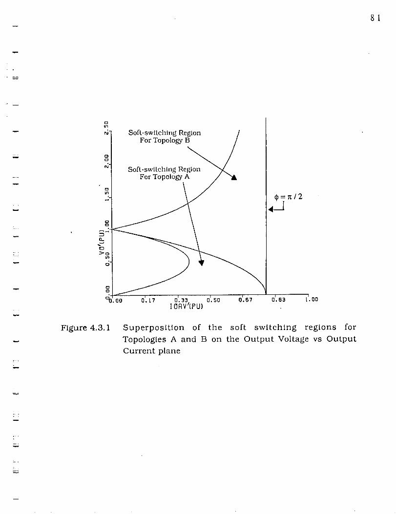
81
w
w
Soft-switching RegionFor Topology B
Soft-switching Region_
For Topology A
w
c:b'.o0 0 • L 7 0 I. 33 0 I. 50 0 • 67 0'. 83 [i. O0
I OAV'[PU)
Figure 4.3. I Superpositlon of the soft switching regions for
Topologies A and B on the Output Voltage vs Output
Current plane
w
w
R

82
u
In conclusion, considering the various desirable features of
Topology B, it seems like the most viable choice as the final topology.
However, the high output voltage requirement(2000 Vdc) seems to
make the use of active output bridges difficult, as devices rated in the
kilovolt range are limited in terms of switching speed. Also, the high
power density needed mandates a high switching frequency. Thus, a
modular approach is necessary for realizing high power at the high
output voltages. For the specified output voltage, a series connection of
two active half-bridges, as shown in Figure 4.3.2, is a possible solution.
These aspects of circuit operation will be examined in the next phase
of the project.
= ,
w
w
w
m
w
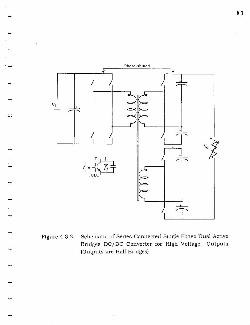
83
. L
w
Vl
u
Phase-shifted
+
r'"
/
)
1
¢_-J0
o
o
o
"7
|
+1
1
r"_
.---k w
4-
vo<
>
Figure 4.3.2 Schematic of Series Connected Single Phase Dual Active
Bridges DC/DC Converter for High Voltage Outputs
(Outputs are Half Bridges)

CHAPTER 5
CONCLUSIONS
w
5.1 Summary
The goal of this project is the development of a high power
density, high power dc/dc converter for aerospace applications. The
rated specifications are an output power of 50 kW, at an input voltage
of 200 Vdc, output voltage of 2000 Vdc, with a power density of 0.2 -
0.3 kg/kW. The switching frequency will be in the order of 50 - 100
kHz. This report describes the work 'h_vol{,ed in the identification and
selection of a suitable converter topology, as a first task of an on-going
research project.
Three new dc/dc converter topologies are proposed, namely
a)- Phase-Shifted Single Active Bridge DC/DC Converter(Topology A)
b) Single Phase Dual Active Bridges DC/DC Converter(Topology B)
c) Three Phase Dual Active Bridges DC/DC Converter(Topology C)
The salient features of these topologies are •
I) All are minimal in structure, i.e., each consists of an input and
output bridge, input and output filter and a transformer, all
components essential for a high power dc/dc conversion
process.
3)
At1 devices of both the bridges can operate under near zero-
voltage conditions, making possible a reduction of device
switching losses and hence, an increase in switching
frequency.J
All circuits operate at a constant frequency, thus simplifying
the task of the magnetic and filter elements.
84

ORIGINAL PAGE IS
OF POOR QUALITY
_4) Since, the leakage inductance of the transformer is used as
the main current transfer element, problems associated with
the diode reverse recovery are eliminated. Also, this mode of
operation allows easy paralleling of multiple modules for
extending the power capacity of the system:
85
w
5) All circuits are least sensitive to parasitic impedances, infact
the parasitics are efficiently utilized.
6) The soft switching transitions, result in low electromagnetic
interference.
In addition, the dual active bridge topologies can realize,
1 ) Two-Quadrant operation
2) Buck-boost charhcteristics
3) Low device and component stresses.
A detailed analysis of each topology has been carried out. The
various steady state operating characteristics including, output voltage,
power transfer, transformer utilization and filter capacitor kVA ratings
as a function of the control and load parameters are presented for soft-
switching conditions.
Based on the analysis, the various device and component ratings
for each topology operating at an optimum point, and under the given
specifications, are tabulated fn Table 4.2.1. Topology A offers the _
possibilty of realizing high output voltages given the fact that the ....
outpdt is a_ diode bridge. However, the input filter capacitor ratings
and device stress-eS are much higher than those for Topologies B and
C. Moreover, the transforrner utiiizati0n is the poorest. On the other
hand, Topologies B and C exhibit device VA stresses-which are only
20% higher than that of an ideal conventional hard switched pwm
converter. Topology B gives a 40% improvement in the transformer
utilization over that of Topology A. Topology C shows a similar

w 86
improvement in the transformer utilization, at the expense of a more
physically complex symmetrical three phase transformer. As expected,
the filter capacitor ratings for Topology C are the lowest.
Based on the following considerations, Topology B is selected as
the final converter topology •
i) Allows better control range, under soft-switching conditions,
as compared to Topology A, especially at a dc conversion ratio
of unity
w
w
l
m
w
m
w
2) Relatively, simpler transformer design as compared to
Topology C
3) Given the state-of-the-art in the high power density multi-
layer ceramic capacitors, it is seen that very little or no
weight penalty will be incurred, although the filter kVA
requirements are higher than that those for Topology C
4) Requires fewer active devices compared to Topology C, and
hence fewer drive circuits
5) Since the control methodology for Topology A can also be
incorporated in Topology B, a much wider range of control
can be achieved.
A fundamental component for the dual active bridge topologies is
also presented, and it shows good correlation to the actual model. This
model allows a better appreciation of soft switching constraints
through phasor diagrams.
w 5.2 Future Work
A proof-of-concept experimental unit for Topology B, rated for 1
kW at a switching frequency of 20 kHz has been built and tested. The

- 87
i
u
w
w
experimental unit along with simulated and actual waveforms showing
soft-switching characteristics will be presented in the next report.
The experimentally obtained power transfer characteristics will also
be presented to corroborate theoretical results.
The tasks involved in the next phase of this project include the
following:
1) Converter Design Issues
a) Choice of device type, based on trade-offs between speed
and conduction losses
b) Computer simulation results with realistic device models,
snubber capacitances and ESRs of filter capacitors
2) Transformer Design Issues
a) Choice of core material based on trade-offs between core
losses, switching frequency and operating flux levels
b) Estimation of copper losses arising from skin and
proximity effects, and investigation of winding geometries
to minimize these losses
c) Investigation of fabrication techniques to control leakage
inductance
w
u
u
m
3) Overall Circuit L_yout Issues
a) For good thermal management
b) For minimization of parasitic impedances
c) For low volume
4) Pr0Jqcted Perf0rmance-Measures
a) Power Density
b) Efficiency

I_FEI_NCF__ & BIBLIOGRAPHY
i
[1]
[2]
[3]
[4[
[5]
[6]
[7]
[8]
[9]
N. Mohan, T. M. Undeland and W. P. Robbins, "Power Electronics-
Converters, Applications, And Design", Textbook, published by
John Wiley & Sons, 1989
F. C. Schwarz and J. B. Klaassens, "A Controllable 45KW Current
Source for DC Machines", IEEE Trans. Ind. Appl., vol. IA-15, no.
4, Jul/Aug 1979, pp. 437-444.
V. T. Ranganathan, P. D. Ziogas and V. R. Stefanovic, "A Regulated
DC/DC Voltage Source Converter using a High Frequency Link", in
Ind. Appl. Soc. Conf. Rec., Oct 1981, pp. 917-924.
R. L. Steigerwald, "High Frequency Resonant Transistor DC/DC
Converters", IEEE Trans. Ind. Elect., vol. IE-31, no. 2, May 1984,
pp. 181-191.
J. G. Kassakian, "A New Current Mode Sine Wave Inverter", IEEE
Trans. Ind. Appl., vol. IA-18, no.3, May/June 1982.
D. M. Divan, "Design Considerations for Very High Frequency
Resonant Mode DC/DC Converters", IEEE Transactions on Power
Electronics, vol. PE-2, no. 1, Jan 1987.
K. H. Liu and F. C. Lee, "Zero-Voltage Switching Technique in
DC/DC Converters", IEEE-PESC 1986 Conf. Rec., pp. 284-289.
K. H. Liu, R. Oruganti and F. C. Lee, "Resonant Switches -
Topologies and Characteristics",IEEE 1985 PESC Record, pp.
106-116.
Y. Cheron, H. Foch and J. Salesses, "Study Of A Resonant
Converter Using Power Transistors In A 25 kW X-Ray Tube Power
Supply", IEEE-PESC, ESA, June 1985, pp. 295-306.
88

- 89
[10] O. D. Patterson and D. M. Divan, "Pseudo-Resonant DC/DC
Converter", IEEE-PESC 1987 Conf. Rec., pp. 424-430.
[11] D. M. Divan, "The Resonant DC Link Inverter - A New Concept In
Static Power Conversion", IEEE-IAS Conf. Records, 1986, pp.
648-656.
[12] R. W. DeDoncker, D. M. Divan and M. H. Kheraluwala, "A Three-
Phase Soft-Switched High Power Density DC/DC Converter for
High Power Applications", IEEE-IAS 1988 Conf. Rec.,pp. 796-
805.
[13] D. M. Divan, "Diodes as Pseudo Active Elements in High
Frequency DC/DC Converters", IEEE-PESC 1988 Conf. Rec., pp.
1024-1030.
[14] M. Ehsani, "Development, Analysis and Control of the Inductor-
Converter Bridge", Ph.D. dissertation, University of Wisconsin,
Madison, May 1981.
[15] M. Ehsani, R. L. Kustom and R. W. Boom, "A One-Phase Dual
Converter for Two-Quadrant Power Control of Super Conducting
Magnets", IEEE Trans. on Magn., vol. MAG-21, no.2, March
1985, pp. 1115-1118.
m
w
[16] R. E. FuJa, R. L. Kustom, and M. Ehsani, "I'hree-Phase Energy
Transfer Circuit with Superconducting Energy Storage Coils",
IEEE Trans. on Ind. Appl., vol. IA-16, no.3, May/June 1980, pp.
438-444.