wide bandgap (wbg) semiconductor power devices … · asd seminar presented at: ... system...
TRANSCRIPT

Wide Bandgap (WBG)
Semiconductor Power Devices for
Switching and RF Power Supplies
Krishna Shenai, PhD
Argonne National Laboratory
ASD Seminar Presented at:
Advanced Photon Source
September 19, 2014
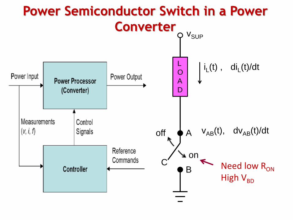
Power Semiconductor Switch in a Power
Converter
L
O
A
D
A
B C
vSUP
iL(t) , diL(t)/dt
vAB(t), dvAB(t)/dt
on
off
Need low RON
High VBD

What is the Role of
Power Electronics in the
Emerging 21st Century
Energy Economy?

Power Electronics Applications
Power Electronics Industry Consortium (PEIC)

Why Wide Bandgap (WBG) Semiconductors?
100
101
102
103
104
105
106
101 102 103 104
Breakdown Voltage (V)
GaN Lateral
SiC Vertical
GaN Vertical
QF2
/ Q
F2 (
Si)
K. Shenai et al, IEEE Trans. Electron Devices, vol. 36, no. 9, pp. 1811-1823, Sep. 1989 K. Shenai et al, ECS J. Solid State Sci. & Technol., vol. 2, no. 8, pp. N3055-N3063, Jul. 2013

W H Y
WBG ?
Increased Energy Efficiency
Smaller Converter Profile
If there is no cost and reliability penalty
Requires higher converter switching frequency and system integration
Reduced Thermal Budget High-temperature semiconductor and improved thermal
management
Wide bandgap (WBG) semiconductors, such as SiC and GaN devices, offer superior electrical and thermal performances compared to silicon
K. Shenai et al, "Optimum Semiconductors for High-Power Electronics," IEEE Trans. Electron Devices, vol. 36, no. 9, pp. 1811-1823, September 1989.
Si is the industry workhorse
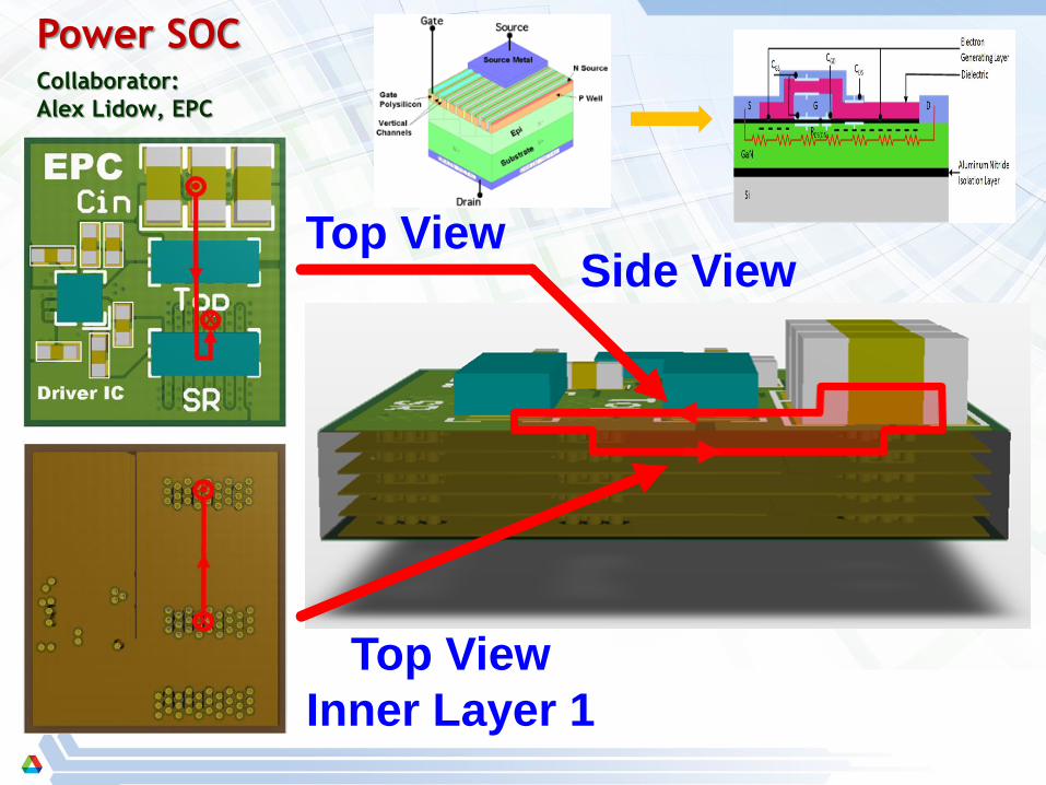
Power SOC
Side View Top View
Top View
Inner Layer 1
Collaborator:
Alex Lidow, EPC

eGaN™ Battery Charger
92
92.5
93
93.5
94
94.5
95
95.5
96
96.5
97
97.5
98
98.5
0 2 4 6 8 10 12 14 16 18 20 22 24 26 28 30 32
Eff
icie
nc
y (
%)
Output Current (A)
Gen 2
eGaN
FETs
Gen 4 eGaN FETs
fsw=300 kHz
fsw=500 kHz
80V MOSFET
VIN=48 V VOUT=12 V

Why Wireless Energy?
• Mobile device charging
• Convenience • Extended battery life
• Medical Implants • Quality of life improvement • Life extender
• Hazardous environment systems • Explosive atmosphere • Corrosive locations • High Voltage

Need to further:
- improve efficiency
- increase transmission range
- reduce cost

DoE’s EV Everywhere
http://energy.gov/sites/prod/files/2014/04/f15/2013_apeem_report.pdf

Hybrid Microgrid
Microgrid
PV Wind
AC grid
Building Lighting, HVAC, hot water
EV charging
Energy storage
Power Electronics is the enabler

13
net effy
i
i ii
i i
i
Power t
Power t
Firming Wind Power With Gas Generator

14
Old
new
Breakthrough solution to deal with variable loads

Old school vs. New school
15
Engine
NG
60 Hz electricity
Dyno
Fixed speed shaft power
Engine
NG 60 Hz electricity
Dyno
AC
DC
DC
AC
Variable speed shaft power
Old
N
ew
DC
net %
- Need WBG power electronics to achieve these efficiency gains. - Even better gains are possible for DC and variable speed drives
Conv 100%
Conv 97%
36.3
36.3
39.6
38.4
3.2%
2.1%
net % Conv Dyno
Engn x x = net
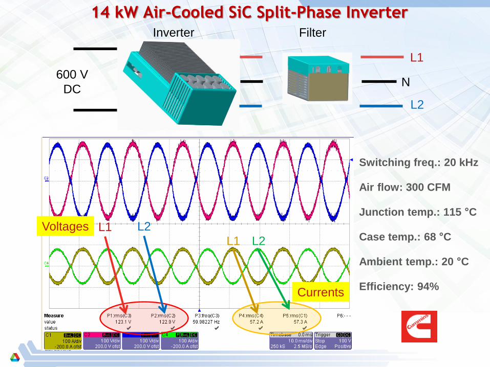
14 kW Air-Cooled SiC Split-Phase Inverter
600 V
DC
L1
L2
N
Inverter Filter
L1 L2 Voltages
Currents
L2 L1
Switching freq.: 20 kHz Air flow: 300 CFM Junction temp.: 115 °C Case temp.: 68 °C Ambient temp.: 20 °C Efficiency: 94%

Test Specifications: • 120/240 V, 60 Hz ac output • 400 V DC input for 6 – 8 kW and 600 V DC input for 10 – 14 kW • Balanced loading conditions • Switching frequency: 20 kHz • Room ambient: 20 °C • Gate drives: SiC MOSFET vGS = +20/–6 V, Si IGBT vGE = +17/–9 V • Temperature data recorded upon reaching thermal steady state of switches
6 8 10 12 14
No Air Flow
6 CFM
24 CFM
90 CFM
300 CFM
25 CFM
45 CFM
240 CFM
>500 CFM
Air Flow TBD
Liquid
Cooling?
Air Flow vs Output Power for Tj = 115 °C
SiC MOSFET Si IGBT
Output Power (kW)
Si inverter range for air flow ≤ 300 CFM
SiC inverter range for air flow ≤ 300 CFM

Measured Inverter Efficiency

OPTION 1
Higher Power
14 kW instead of 10 kW
OPTION 2
Smaller Cooling
@ 10 kW
OPTION 3
Higher Frequency
@ 8 kW
Si
Inverter
10 kW @ 90% efficiency 240 CFM 20 kHz switching
SiC
Inverter
14 kW @ 94% efficiency
24 CFM
50 kHz switching
20 kHz switching freq.
≤ 300 CFM Air Flow
115 °C junction temperature
40% more power (kW↑)
4% more efficiency
20 kHz switching freq.
115 °C junction
temperature
90% lesser
cooling ($↓)
Estimated 30%
reduction in filter
cost and size
($↓)
Design Options to Reduce System-Level $/kW
All options reduce: Total System Cost ($) Output Power (kW)

Lateral GaN Power Transistors – Emerging Breakthrough Technology
Parameter CoolMOS Si IGBT GaN Cascode GaN E-HEMT
Rating (V/I) 700/28 600/60 600/17 650/30
RON (mΩ) 70 40 150 52
QG (nC) 64 165 6.2 6.5
ESW (μJ) 2300 1380 500 150
Tjmax (°C) 150 150 150 150
Need External Body Diode?
Yes Yes Yes No Bidirectional
Module
Recommend R&D with: 600V/200A single-chip and 600V/1000A module from GaN Systems. Need to evaluate reliability
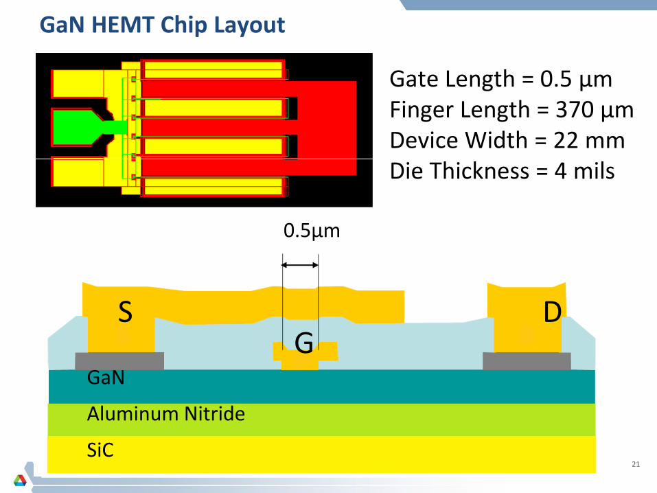
GaN HEMT Chip Layout
21
G S D
0.5μm
GaN
Aluminum Nitride
SiC
Gate Length = 0.5 µm Finger Length = 370 µm Device Width = 22 mm Die Thickness = 4 mils

22
0 0.5 1 1.5 2 2.5 3
-1
0
1
2
3
-1
0
1
2
3
0 0.5 1 1.5 2 2.5 3
Measured Model
S11 S22
100 MHz – 3 GHz Modeled Measured
S21
Frequency (GHz)
VDS = 48V IDSQ = 430 mA

Two Stages Combined – Each Stage Terminates in 25 Ohms
23

24
0 0.5 1
-15
-10
-5
0
5
10
15
20
-15
-10
-5
0
5
10
15
20
0 0.5 1 1.5 2 2.5 3
Actual Loss Actual Gain
Modeled loss Modeled Gain
Frequency (GHz)
Gai
n (
dB
)
Ret
urn
Lo
ss (
dB
)
VDS = 48V IDSQ = 400 mA

25
-5 5 15 25 35 45
2
4
6
8
10
12
14
16
10
15
20
25
30
35
40
45
50
0 10 20 30 40
Actual Power
Modeled Gain
Modeled Power
Actual Gain
PIN (dbm)
PO
UT
(db
m)
Gai
n (
dB
)
Frequency = 200 MHz
VDS = 48V IDSQ = 450 mA
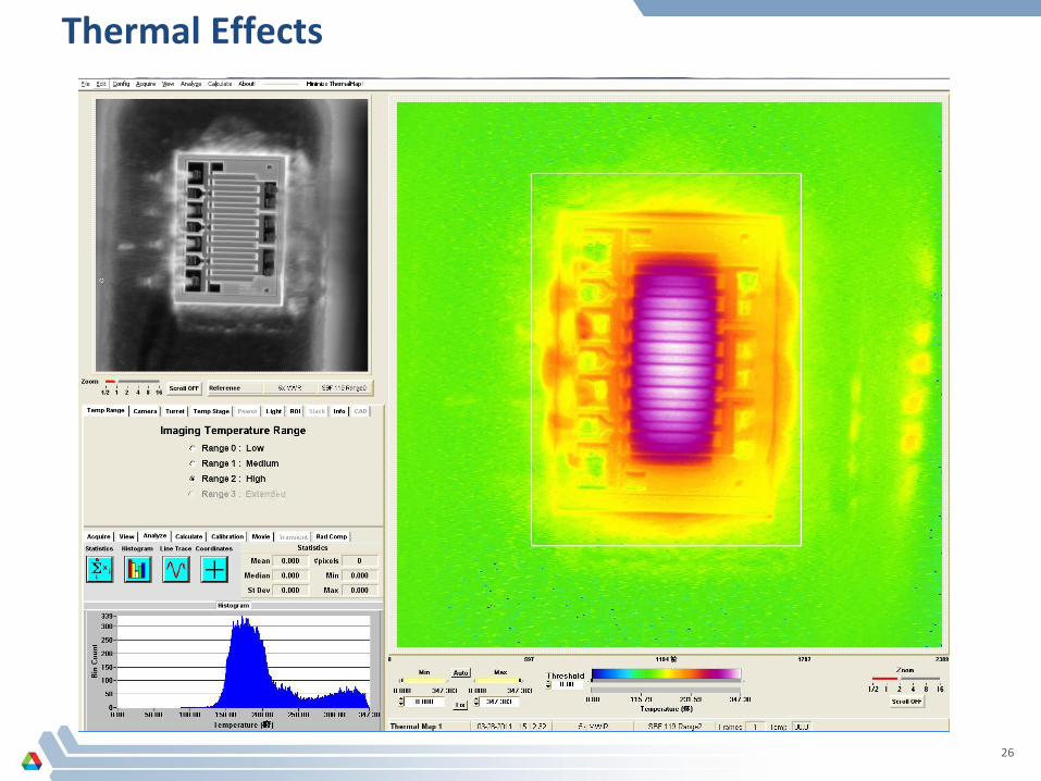
Thermal Effects
26

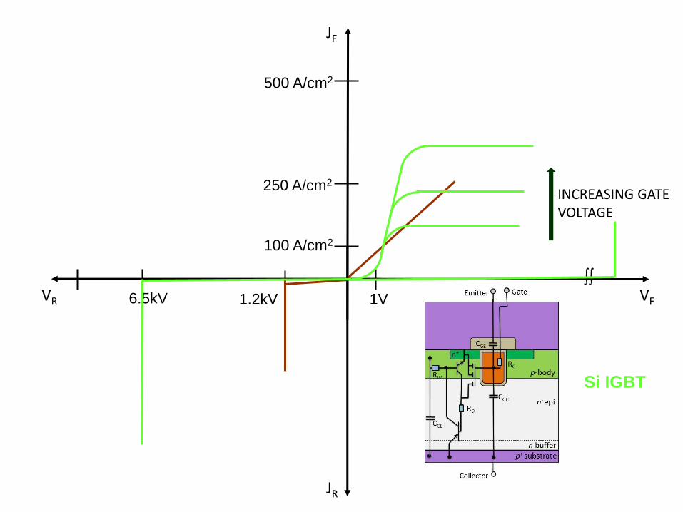
The Search for the Ideal Semiconductor Power Switch (dates back to the 1950’s)
Power Circuit
JF
JR
VF VR
ACTIVE REGION
REVERSE CHARACTERISTICS
FORWARD CHARACTERISTICS
BLOCKING REGION
FOR REPETITIVE
SWITCHING WITHOUT
FAILURE IN THE FIELD
100kV 100kV
2000 A/cm2

∫∫ 1.2kV 1V
500 A/cm2
250 A/cm2
100 A/cm2
JF
JR
VF VR
Si MOSFET
INCREASING GATE VOLTAGE
∫∫
1.2kV 6.5kV 1V
500 A/cm2
250 A/cm2
100 A/cm2
JF
JR
VF VR
Si IGBT
INCREASING GATE VOLTAGE
∫∫
1kV 6.5kV 1V
500 A/cm2
250 A/cm2
100 A/cm2
JF
JR
VF VR
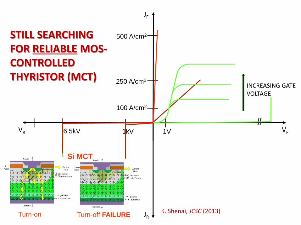
INCREASING GATE VOLTAGE
Si MCT
Turn-on Turn-off FAILURE
STILL SEARCHING FOR RELIABLE MOS-CONTROLLED THYRISTOR (MCT)
K. Shenai, JCSC (2013)
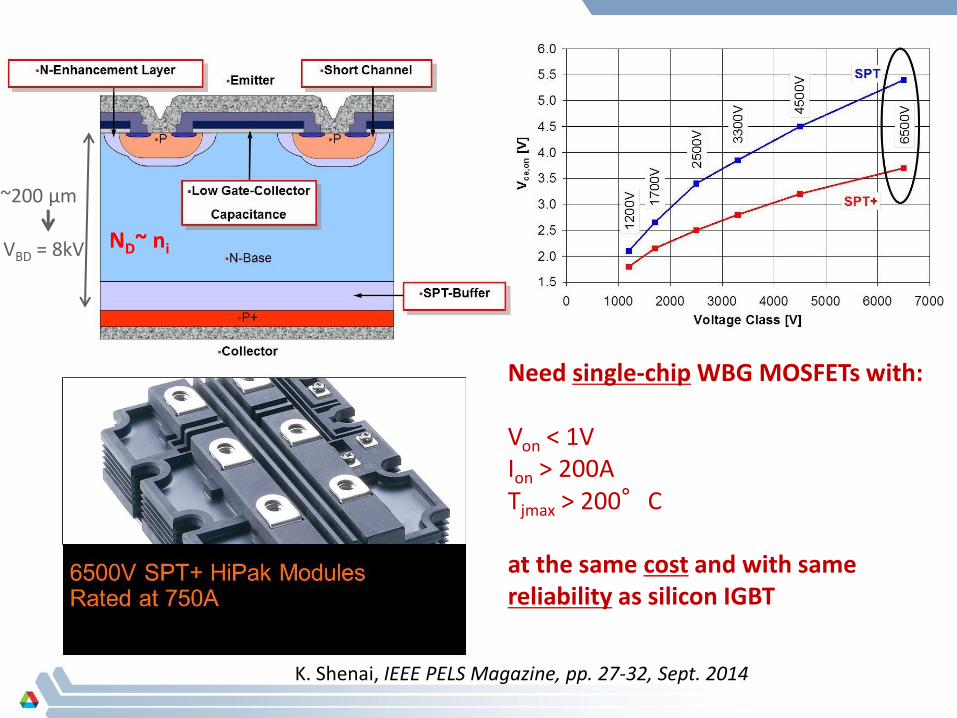
Need single-chip WBG MOSFETs with: Von < 1V Ion > 200A Tjmax > 200°C at the same cost and with same reliability as silicon IGBT
~200 μm
VBD = 8kV ND~ ni
K. Shenai, IEEE PELS Magazine, pp. 27-32, Sept. 2014

∫∫
10kV 35kV 1V
1500 A/cm2
1000 A/cm2
100kV
500 A/cm2
JF
JR
VF VR
INCREASING GATE VOLTAGE
Why WBG?
LOW COST SWITCH
FOR REPETITIVE
SWITCHING
WITHOUT FAILURE
IN THE FIELD
K. Shenai et al, "Optimum Semiconductors for High-Power Electronics," IEEE Trans. Electron Devices, vol. 36, no. 9, pp. 1811-1823, September 1989.
∫∫

Key Challenges and Opportunities
• High chip and module costs • Non-optimal performance • Long-term reliability in a power
converter unknown
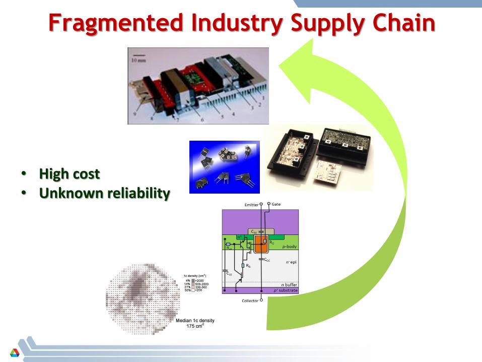
Fragmented Industry Supply Chain
• High cost • Unknown reliability

Parameter Silicon SiC
Growth Temperature
< 1000°C > 2000°C
Method Czochralski PVT
Defect Density < 1/cm2 102 – 104 cm-2
Cost Low > 20X
Expensive and Defective Wafers

Stony Brook Synchrotron Topography Facility Beamline X-19C
Department of Materials Science & Engineering
Substrate Dislocation Density Trends (collaborator: Dr. Mike Dudley, SUNY-SB)
0
5000
10000
15000
20000
25000
30000
35000
40000
45000
2000 2002 2004 2006 2008 2010 2012 2014
Dislocation Density(cm-2)
0
5000
10000
15000
20000
25000
30000
35000
40000
45000
2000 2002 2004 2006 2008 2010 2012 2014
BPD Density(cm-2)
0
500
1000
1500
2000
2500
3000
3500
4000
4500
2000 2002 2004 2006 2008 2010 2012 2014
TSD Density(cm-2)
0
500
1000
1500
2000
2500
3000
3500
4000
4500
5000
2000 2002 2004 2006 2008 2010 2012 2014
TED Density(cm-2)

Micropipes
(a) (b) (c) High resolution synchrotron monochromatic X-ray topographs recorded at Argonne’s Advanced Photon Source (APS) facility. (a) Back-reflection X-ray topograph (g = 0004) images of close-core threading screw dislocations (TSDs) and basal plane dislocations (BPDs) in a (0001) 4H SiC wafer; (b) Grazing incidence X-ray topograph (g = 11-28) of 4H-SiC substrate showing TSDs (right and left handed) and TEDs; (c) Transmission X-ray topograph showing the images of BPDs.
Defects in State-of-the-Art Commercial 4H-SiC Wafers (collaborator: Dr. Mike Dudley, SUNY-SB)

Performance Evaluation of 4H-SiC JBS Power Diode
K. Shenai, IEEE Trans. ED, Feb. 2015 (to be published)

Defect-Induced Lattice Deformation in 600V SiC JBS Diode
Defect delineation study performed using hard X-rays at Argonne’s Advanced Photon Source (APS). At 900V reverse bias, TSDs in the vicinity of the metal- semiconductor junction were excited and acted as charge generation centers that caused diode breakdown.
(collaborator: Dr. Mike Dudley, SUNY-SB)
K. Shenai et al, Science (to be published)

Reliability Evaluation of SiC Power Diode
Jabali et al, Appl. Phys. Lett.101, 22 (2012)
Acharya and Shenai, PET Conf., 672-277 (2002) Shenai et al, IEEE Proc., 35-52, Jan. 2014
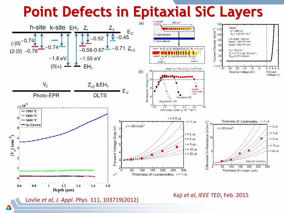
Point Defects in Epitaxial SiC Layers
Kaji et al, IEEE TED, Feb. 2015 Lovlie et al, J. Appl. Phys. 111, 103719(2012)

Influence of Threading Dislocations on Lifetime of Gate Thermal Oxide in SiC MOSFETs
Yamamoto et al, Mater. Sci. Forum., 717-720, pp 477-480, (2012)
Time Dependent Dielectric Breakdown (TDDB) detected through photo-emission. Defects
responsible for the breakdown, i.e., at breakdown location revealed by etching and x-sectional
TEM:
•Mode A : Intrinsic breakdown (no crystallographic defect);
•Mode B: due to TEDs – lifetime shortened by one order of magnitude;
•Mode C (shortest Lifetime): due to TSDs – lifetime shortened by two orders of magnitude
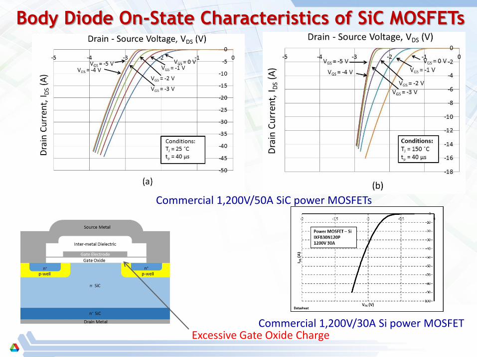
Body Diode On-State Characteristics of SiC MOSFETs
Excessive Gate Oxide Charge
Commercial 1,200V/50A SiC power MOSFETs
Commercial 1,200V/30A Si power MOSFET

Safe Operating Area (SOA)
Device type SOA (in kW)
Silicon (IXYS) 72.4
Silicon Carbide (CREE) 52.7
Silicon Carbide (ST) 59.6
IXFB30N120P (Si) VDSS = 1200V ID25 = 30A RDS(on) ≤ 350mΩ trr ≤ 300ns
C2M0080120D (SiC) VDS 1200 V ID @ 25˚C 31.6 A RDS(on) 80 mΩ
SCT30N120 (SiC) VDS 1200 V ID @ 25˚C 45 A RDS(on) 80 mΩ
1
10
100
1000
1 10 100 1000 10000
Dra
in C
urr
en
t, I
D (
A)
Drain-Source Voltage, VDS (V)
IXYS_1200 V (Si)
Cree_1200 V (SiC)
ST_1200 V (SiC)
Condition : Tc = 25˚C Tj = 150˚C tp = 100 μs
K. Shenai, IEEE Trans. ED, Feb. 2015 (to be published)

Similar image, lower defect density region.
Image from longitudinal slice showing the seed/crystal interface region
(indicated by arrows) in a 6H-SiC crystal grown by Physical Vapor
Transport. One-to-one correlation can be found between [0001] screw
dislocations in the seed and in the newly grown crystal. Dislocations of
various Burgers vector can be observed (b=[0006] to b~5[0001])
Dislocations and Micropipes in SiC
SEM
2
2
4
bD
: shear modulus
: surface energy
From J. Bohm. Realstruktur
von Kristallen. E.
Schweizerbart'sche
Verlagsbuchhandlung (Nägele
u. Obermiller), Stuttgart 1995
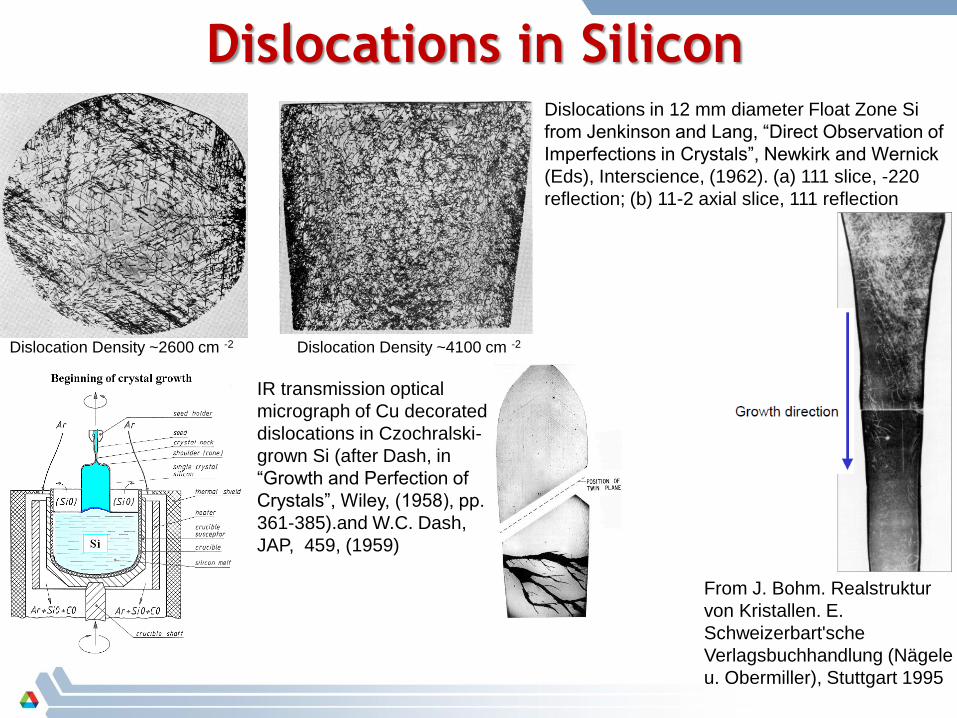
Dislocations in Silicon Dislocations in 12 mm diameter Float Zone Si
from Jenkinson and Lang, “Direct Observation of
Imperfections in Crystals”, Newkirk and Wernick
(Eds), Interscience, (1962). (a) 111 slice, -220
reflection; (b) 11-2 axial slice, 111 reflection
IR transmission optical
micrograph of Cu decorated
dislocations in Czochralski-
grown Si (after Dash, in
“Growth and Perfection of
Crystals”, Wiley, (1958), pp.
361-385).and W.C. Dash,
JAP, 459, (1959)
Dislocation Density ~2600 cm -2 Dislocation Density ~4100 cm -2

Can we build
“Taj Mahal”
on a cracky foundation and
expect it to remain intact for
centuries?

Summary and Recommendations
• Wide bandgap (WBG) power semiconductor devices with superior performance than silicon are instrumental for 21st century energy economy.
• Cost of WBG power devices needs to be reduced, performance optimized,
and field-reliability demonstrated.
• Fundamental challenge pertains to the starting material – low defect density, large-area substrates and epi layers are needed – low-temperature growth techniques.
• Radically new homo-epitaxial (for vertical devices) wafer synthesis and MOS
channel formation methods need to be developed.
• The role of defects in the ground and excited states needs to be fully understood.
• Failure physics should be investigated and new reliability assessment techniques need to be developed.

Thank you!
Any Questions?