who’s getting the cash in...
TRANSCRIPT

WHO’S GETTING THE CASH IN
NANOMANUFACTURING?Douglas W. Jamison
Harris & Harris Group, Inc.One Rockefeller Center, Suite 1430
New York, NY 10020(212) 332-3600 [email protected]
PRESENTATION:
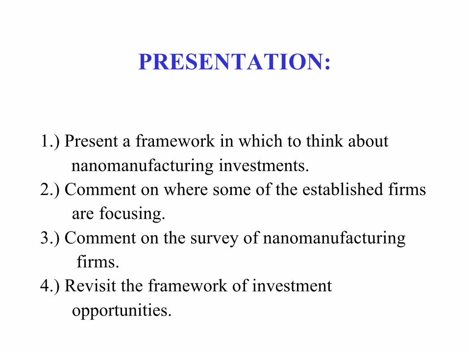
1.) Present a framework in which to think about nanomanufacturing investments.
2.) Comment on where some of the established firmsare focusing.
3.) Comment on the survey of nanomanufacturingfirms.
4.) Revisit the framework of investmentopportunities.
PREFACE:
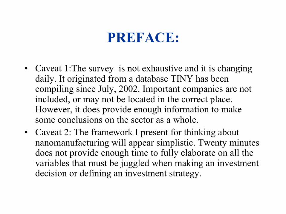
• Caveat 1:The survey is not exhaustive and it is changing daily. It originated from a database TINY has been compiling since July, 2002. Important companies are not included, or may not be located in the correct place. However, it does provide enough information to make some conclusions on the sector as a whole.
• Caveat 2: The framework I present for thinking about nanomanufacturing will appear simplistic. Twenty minutes does not provide enough time to fully elaborate on all the variables that must be juggled when making an investment decision or defining an investment strategy.
PREFACE:
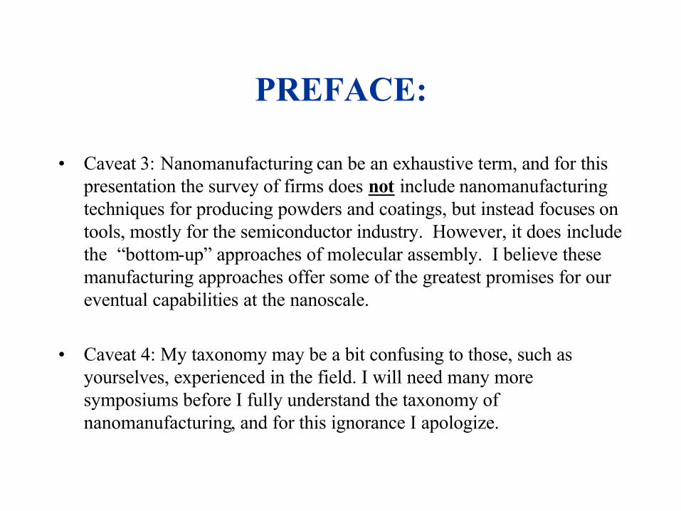
• Caveat 3: Nanomanufacturing can be an exhaustive term, and for this presentation the survey of firms does not include nanomanufacturingtechniques for producing powders and coatings, but instead focuses on tools, mostly for the semiconductor industry. However, it does include the “bottom-up” approaches of molecular assembly. I believe these manufacturing approaches offer some of the greatest promises for our eventual capabilities at the nanoscale.
• Caveat 4: My taxonomy may be a bit confusing to those, such as yourselves, experienced in the field. I will need many more symposiums before I fully understand the taxonomy of nanomanufacturing, and for this ignorance I apologize.
FRAMEWORK:
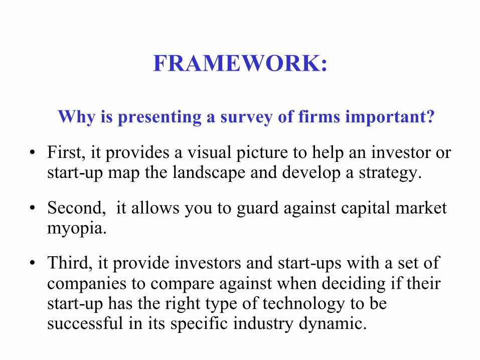
Why is presenting a survey of firms important?
• First, it provides a visual picture to help an investor or start-up map the landscape and develop a strategy.
• Second, it allows you to guard against capital market myopia.
• Third, it provide investors and start-ups with a set of companies to compare against when deciding if their start-up has the right type of technology to be successful in its specific industry dynamic.

FRAMEWORK:
My strategy for thinking of investments in nanomanufacturing after mapping the landscape is as follows:
• Look for companies that have a novel manufacturing capability but that focus on a high value application for which this capability can be leveraged and applied.
• Concentrate on “bottom-up” and similar approaches that take advantage of key properties or potentials at the nanoscale.
• Look for “disruptive technologies” (as precisely defined by Clayton Christensen) that have established their first key niche and have established partnerships validating the performance metric in this niche.

FRAMEWORK:Capital Market Myopia:
• William Sahlman and Howard Stevenson developed this terminology in a case study presenting the Winchester hard-disk-drive industry. It was developed and included by William Bygrave and Jeffrey Timmons in their classic book, Venture Capital at the Crossroads.
• Capital market myopia leads to the over-funding of technology firms in industries, and unsustainable levels of valuation in the stock market.
• Leads to the “Impossibility Theorem.” The amount of value that must be created at any point in time for investors to achieve a target rate of return (based on capital committed to an industry) becomes impossible to achieve. (April 23, 2003 article in the Wall Street Journal on what it would take to have Ebay match the analysts’ targets in 2010.)
• The return necessary for risky investments in new start-ups cannot be achieved. The result: Future consolidation and the loss of investments.
• Investors don’t want to help create nor participate in an industry undergoing capital market myopia – but we continually seem to do just this.
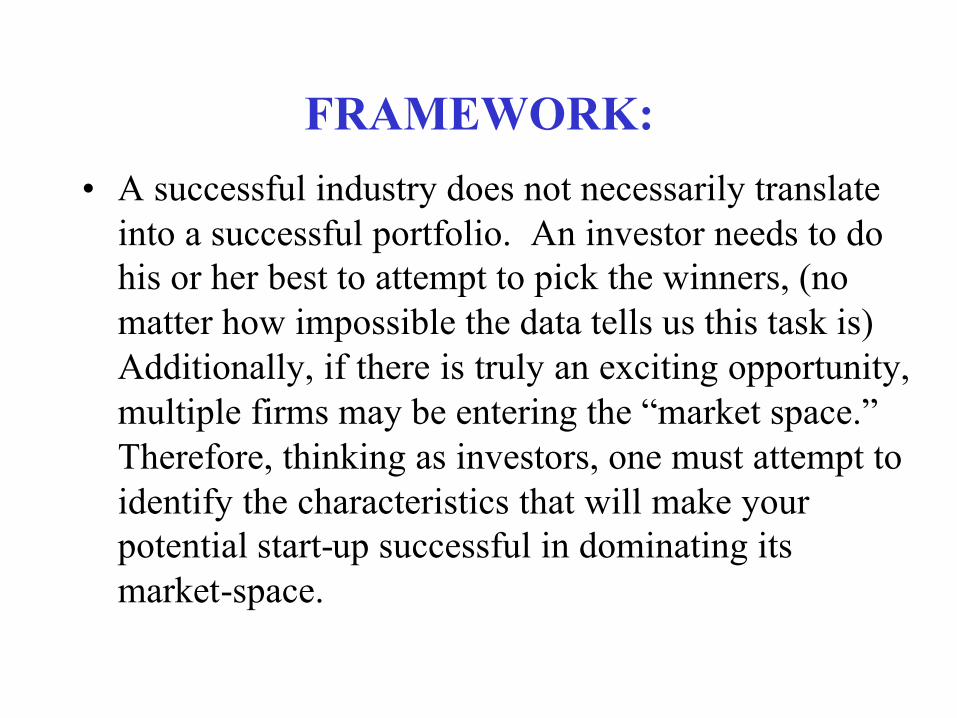
FRAMEWORK:• A successful industry does not necessarily translate
into a successful portfolio. An investor needs to do his or her best to attempt to pick the winners, (no matter how impossible the data tells us this task is) Additionally, if there is truly an exciting opportunity, multiple firms may be entering the “market space.” Therefore, thinking as investors, one must attempt to identify the characteristics that will make your potential start-up successful in dominating its market-space.

FRAMEWORK:
• I won’t spend the time during this presentation to really go through the survey of companies that I will show you. However, I provide it for future reference.
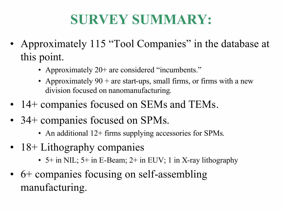
SURVEY SUMMARY:
• Approximately 115 “Tool Companies” in the database at this point.
• Approximately 20+ are considered “incumbents.”• Approximately 90 + are start-ups, small firms, or firms with a new
division focused on nanomanufacturing.
• 14+ companies focused on SEMs and TEMs.• 34+ companies focused on SPMs.
• An additional 12+ firms supplying accessories for SPMs.
• 18+ Lithography companies• 5+ in NIL; 5+ in E-Beam; 2+ in EUV; 1 in X-ray lithography
• 6+ companies focusing on self-assembling manufacturing.

CURRENT FIRMS DEVELOPING
NANOMANUFACTURING CAPABILITIES:
“THE INCUMBENTS”

THE INCUMBENTS:• The established players pretty well cover the areas of electron
microscopy (FEI, Hitachi, JEOL, LEO, Seiko), SPM (VEECO, JMAR, Nikon, Olympus, Zeiss) and most lithography techniques (ASML, Canon, HP, Nikon, UltratechStepper). Additionally, they provide metrology and inspection tools and manufacture process control equipment.
• I believe these companies will continue to lead the field in these technologies. Regardless of whether future advancements are incremental or radical in nature, I believe these companies have the best resources for introducing these advancements and protecting their domain. To support this I would direct you to Clayton Christensen’s research on the introduction of sustaining technologies in multiple industries.
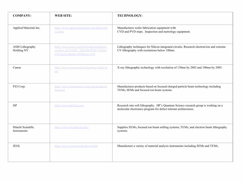
COMPANY: WEB SITE: TECHNOLOGY:
Applied Materials Inc. http://www.appliedmaterials.com/about/index.html
Manufactures wafer fabrication equipment withCVD and PVD steps. Inspection and metrology equipment.
ASM Lithography Holding NV
http://www.asml.com/NASApp/asmldotcom/show.do?GXHC_JSESSIONID=383da70197aa2e53&rid=1839&ctx=238
Lithography techniques for Silicon integrated circuits. Research electron/ion and extreme UV lithography with resolutions below 100nm.
Canon http://www.canon.com/technology/index.html
X-ray lithographic technology with resolution of 130nm by 2003 and 100nm by 2005.
FEI Corp. http://www.feicompany.com/eng/products/list.html
Manufactures products based on focused charged particle beam technology including TEMs, SEMs and focused ion beam systems.
HP http://www.hpl.hp.com/ Research into soft lithography. HP’s Quantum Science research group is working on a molecular electronics program for defect tolerant architectures.
Hitachi Scientific Instruments
http://www.hii-hitachi.com/ Supplies SEMs, focused ion beam milling systems, TEMs, and electron beam lithography systems.
JEOL http://www.jeol.com/products.html Manufacture a variety of material analysis instruments including SEMs and TEMs.
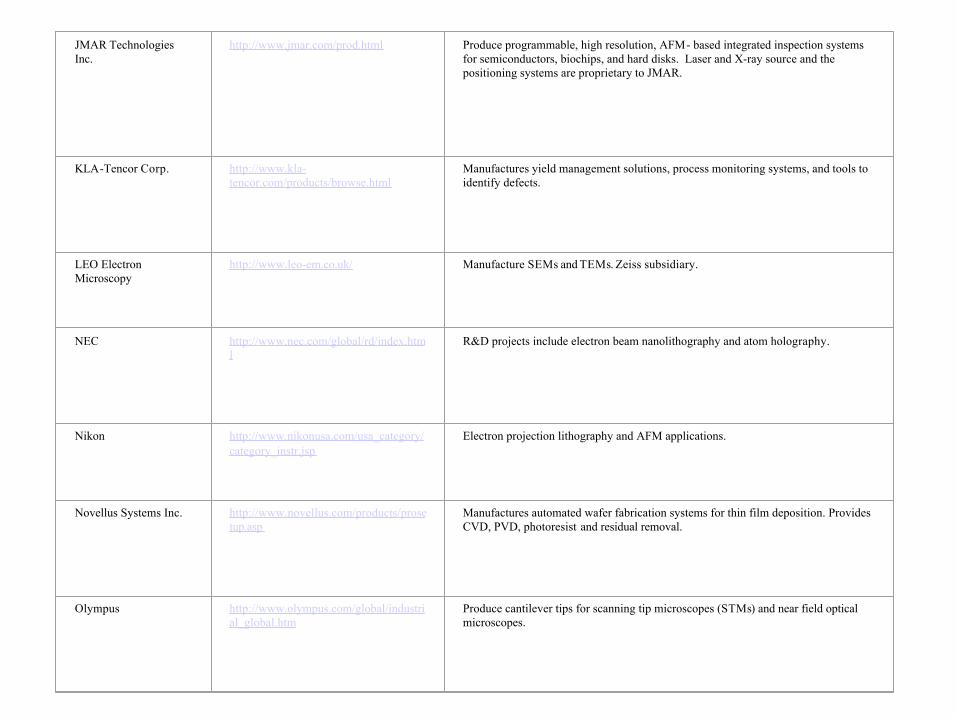
JMAR Technologies Inc.
http://www.jmar.com/prod.html Produce programmable, high resolution, AFM- based integrated inspection systems for semiconductors, biochips, and hard disks. Laser and X-ray source and the positioning systems are proprietary to JMAR.
KLA-Tencor Corp. http://www.kla-tencor.com/products/browse.html
Manufactures yield management solutions, process monitoring systems, and tools to identify defects.
LEO Electron Microscopy
http://www.leo-em.co.uk/ Manufacture SEMs and TEMs. Zeiss subsidiary.
NEC http://www.nec.com/global/rd/index.html
R&D projects include electron beam nanolithography and atom holography.
Nikon http://www.nikonusa.com/usa_category/category_instr.jsp
Electron projection lithography and AFM applications.
Novellus Systems Inc. http://www.novellus.com/products/prosetup.asp
Manufactures automated wafer fabrication systems for thin film deposition. Provides CVD, PVD, photoresist and residual removal.
Olympus http://www.olympus.com/global/industrial_global.htm
Produce cantilever tips for scanning tip microscopes (STMs) and near field optical microscopes.

Rudolph Technologies Inc.
http://www.rudolphtech.com/products/index.html
Manufactures process control metrology systems including a metrology line for opaque and transparent films.
Seiko Instruments http://www.sii.co.jp/info/eg/index.html Manufactures analytical equipment including scanning probe microscopes, focused ion beam machines and SEMs.
Ultratech Stepper Inc. http://www.ultratech.com/products/index.shtml
Manufactures photolithography equipment.
Veeco Instruments Inc.Digital Instruments
http://www.veeco.com/html/product_bymarket.asp
Manufactures process equipment and metrology tools including etch and deposition systems and surface measurement systems.DI manufactures scanning probe microscopes, AFMs, near field scanning optical microscopes, and related peripherals.
Zeiss http://www.zeiss.com/us/home.nsf/Contents-FrameDHTML/F2F21D215D97061C85256CAD0054C9B3
Manufacturer of optical microscopes, SPMs and SEMs. LEO is a subsidiary.
CURRENT FIRMS DEVELOPING
NANOMANUFACTURING CAPABILITIES:
“THE UP AND COMING?”
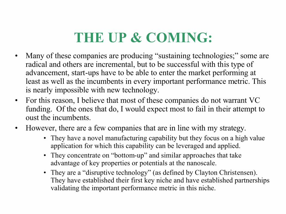
THE UP & COMING:• Many of these companies are producing “sustaining technologies;” some are
radical and others are incremental, but to be successful with this type of advancement, start-ups have to be able to enter the market performing at least as well as the incumbents in every important performance metric. This is nearly impossible with new technology.
• For this reason, I believe that most of these companies do not warrant VC funding. Of the ones that do, I would expect most to fail in their attempt to oust the incumbents.
• However, there are a few companies that are in line with my strategy.• They have a novel manufacturing capability but they focus on a high value
application for which this capability can be leveraged and applied.• They concentrate on “bottom-up” and similar approaches that take
advantage of key properties or potentials at the nanoscale.• They are a “disruptive technology” (as defined by Clayton Christensen).
They have established their first key niche and have established partnerships validating the important performance metric in this niche.
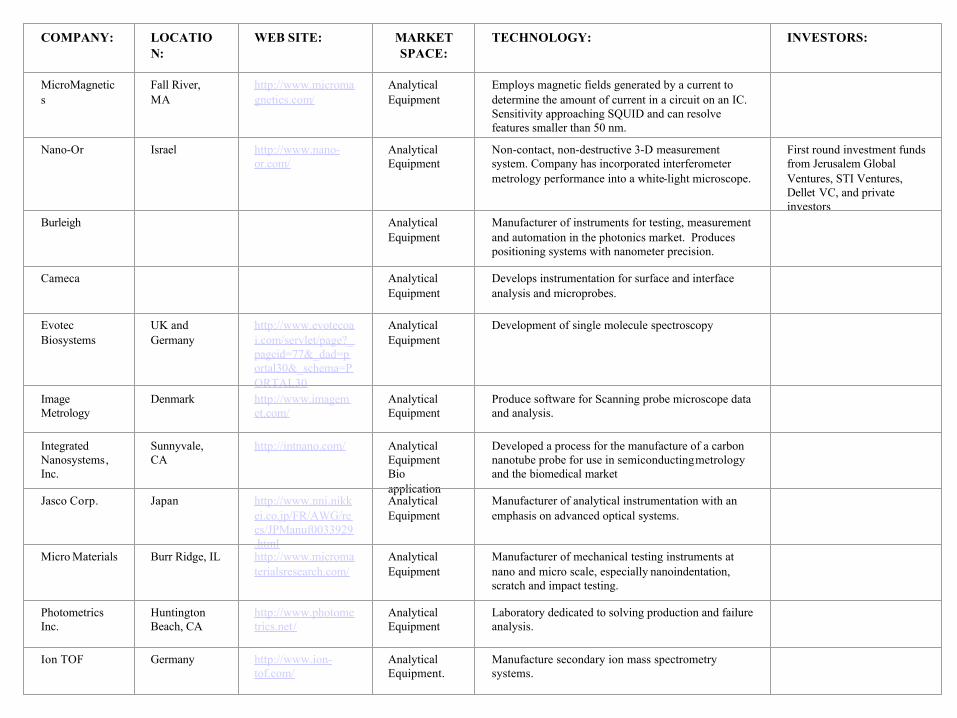
COMPANY: LOCATION:
WEB SITE: MARKETSPACE:
TECHNOLOGY: INVESTORS:
MicroMagnetics
Fall River, MA
http://www.micromagnetics.com/
Analytical Equipment
Employs magnetic fields generated by a current to determine the amount of current in a circuit on an IC. Sensitivity approaching SQUID and can resolve features smaller than 50 nm.
Nano-Or Israel http://www.nano-or.com/
Analytical Equipment
Non-contact, non-destructive 3-D measurement system. Company has incorporated interferometer metrology performance into a white-light microscope.
First round investment funds from Jerusalem Global Ventures, STI Ventures, Dellet VC, and private investors
Burleigh Analytical Equipment
Manufacturer of instruments for testing, measurement and automation in the photonics market. Produces positioning systems with nanometer precision.
Cameca Analytical Equipment
Develops instrumentation for surface and interface analysis and microprobes.
EvotecBiosystems
UK and Germany
http://www.evotecoai.com/servlet/page?_pageid=77&_dad=portal30&_schema=PORTAL30
Analytical Equipment
Development of single molecule spectroscopy
Image Metrology
Denmark http://www.imagemet.com/
Analytical Equipment
Produce software for Scanning probe microscope data and analysis.
Integrated Nanosystems, Inc.
Sunnyvale, CA
http://intnano.com/ Analytical EquipmentBio application
Developed a process for the manufacture of a carbon nanotube probe for use in semiconductingmetrology and the biomedical market
Jasco Corp. Japan http://www.nni.nikkei.co.jp/FR/AWG/recs/JPManuf0033929.html
Analytical Equipment
Manufacturer of analytical instrumentation with an emphasis on advanced optical systems.
Micro Materials Burr Ridge, IL http://www.micromaterialsresearch.com/
Analytical Equipment
Manufacturer of mechanical testing instruments at nano and micro scale, especially nanoindentation, scratch and impact testing.
PhotometricsInc.
Huntington Beach, CA
http://www.photometrics.net/
Analytical Equipment
Laboratory dedicated to solving production and failure analysis.
Ion TOF Germany http://www.ion-tof.com/
Analytical Equipment.
Manufacture secondary ion mass spectrometry systems.
Positron Systems Inc.
Boise, ID http://www.positronsystems.com/
Metrology and Inspection Tool
Non-destructive technology for identifying nanoscale defects called Photon Induced Positron Annihilation System.
Rave LLC Delray Beach, FL
http://www.ravellc.com/careers.html
Metrology and Inspection Tool.
Developing a scanning probe microscope tool for mask and semiconductor repair.
Nano World Technologies
Metrology/ Inspection Tool
Electron beam nanolithography used to inspect and repair semiconductor photomasks.
Nanometrology New York Metrology/ Inspection Tool
CD-SEM calibration and line-edge roughness metrology tool to help technicians calibrate multiple CD-SEMs for increased yields.
NLine Corp. Austin, TX http://www.nline.com/
Metrology/ Inspection Tool
Digital holography to peer into narrow and deep spaces such as contacts and trench capacitors on semiconductor wafers. Tool detects defects that are smaller than the wavelength of deep ultraviolet light. Targeted at 90 nm process technology.
$7.4 million second round included Advanced Micro Devices, Hat Creek Partners, Intel Capital, Sensor Technology Development Fund, SG Cowen Venture Partners, TAT Capital Partners Ltd., and Thomas WeiselPartners. The $7.4 million raised brings the total equity investment in nLine to $18.4M.
Therma-Wave SanFrancisco, CA
http://www.thermawave.com/
Metrology/ Inspection Tool
Develop a real time, critical dimension system to scatterometrically measure 130 nm photoresistfeatures for polysilicon gate and shallow trench applications.
Established since 1982
Hysitron Minneapolis, MN
http://www.hysitron.com/
Metrology/ Inspection Tool
Manufactures nanomechanical testing instruments especially tailored to measure hardness, elastic modulus, friction, wear resistance, fatigue, nanoscratch and indentation.
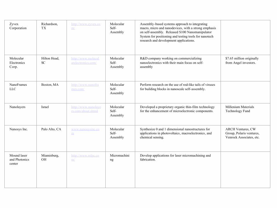
ZyvexCorporation
Richardson, TX
http://www.zyvex.com/
Molecular Self-Assembly
Assembly-based systems approach to integrating macro, micro and nanodevices, with a strong emphasis on self-assembly. Released S100 NanomanipulatorSystem for positioning and testing tools for nanotech research and development applications.
Molecular Electronics Corp.
Hilton Head, SC
http://www.molecularelectronics.com/
Molecular Self-Assembly
R&D company working on commercializing nanoelectronics with their main focus on self-assembly
$7.65 million originally from Angel investors.
NanoFramesLLC
Boston, MA http://www.nanoframes.com/
Molecular Self-Assembly
Perform research on the use of rod-like tails of viruses for building blocks in nanoscale self-assembly.
Nanolayers Israel http://www.nanolayers.com/about.shtml
Molecular Self-Assembly
Developed a proprietary organic thin-film technology for the enhancement of microelectronic components.
Millenium Materials Technology Fund
Nanosys Inc. Palo Alto, CA www.nanosysinc.com
Molecular Self-Assembly
Synthesize 0 and 1 dimensional nanostructures for applications in photovoltaics, macroelectronics, and chemical sensing.
ARCH Ventures, CW Group, Polaris ventures, Venrock Associates, etc.
Mound laser and Photonics center
Miamisburg, OH
http://www.mlpc.com/
Micromachining
Develop applications for laser micromachining and fabrication.
Molecular Imprints
Austin, TX http://www.molecularimprints.com/aboutmi.html
Nanoimprint Lithography
Step & Flash Imprint Lithography. Imprio 100 has a price tag of $2 million.
$12 million in VC funding from Alloy Ventures, Asset Management, DFJ, Huntington Ventures, KT Venture Group, Lam research and Motorola Ventures
Nanonex Corp. Princeton, NJ http://www.nanonex.com/
Nanoimprint Lithography
Shipping nanoimprint lithography tools ranging in price from $300-700K.
undisclosed
Obducat AB Malmo, Sweden
http://www.obducat.com/sida_2.asp
Nanoimprint Lithography
Develop and supply technologies for the production of advanced micro and nano structures for research and manufacturing including electron beam writers, electron microscopes and nanolithography. Sold 5 pilot production NIL machines with 20-25 to be delivered to customers in 2003.
Public company
EV Group Austria http://www.evgroup.com/products/hotembossing.htm
Nanoimprint Lithography
A semiconductor and MEMS production equipment maker. EV Group has three nanoimprint lithography systems, the hot embossing device that works at high temperatures and precise pressure, a device that solidifies the polymer material with UV light and a microcontactingprinting process that uses a flexible stamp to deposit patterns on surfaces with existing topographical features.
LumArray Cambridge, MA
http://www.lumarray.com/index.htm
Next Generation Lithography
Maskless zone plate array lithography controlled by Microsystems. Technology is extendable to 10-20 nm.
Advantest Japan http://www.advantest.co.jp/products/en-index.shtml
Next Generation Lithography
Manufacture electronic measuring instruments, automatic test equipment and electron beam lithography systems for ICs.
AMO GmbH Germany http://www.amo.de/amo/welcome_en.html
Next Generation Lithography
Develop interference lithography and nanoimprint technology
NanoInk Chicago, IL http://www.nanoink.net/home.html
Next generation Lithography
AFM based dip-pen lithography* Raised approximately $6 million Galway partners and Lorie Investment Fund
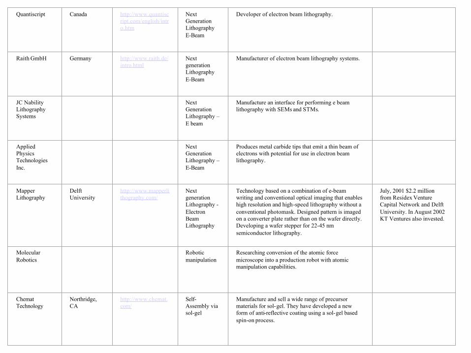
Quantiscript Canada http://www.quantiscript.com/english/intro.htm
Next Generation LithographyE-Beam
Developer of electron beam lithography.
Raith GmbH Germany http://www.raith.de/intro.html
Next generation LithographyE-Beam
Manufacturer of electron beam lithography systems.
JC NabilityLithography Systems
Next Generation Lithography –E beam
Manufacture an interface for performing e beam lithography with SEMs and STMs.
Applied Physics Technologies Inc.
Next Generation Lithography –E-Beam
Produces metal carbide tips that emit a thin beam of electrons with potential for use in electron beam lithography.
MapperLithography
Delft University
http://www.mapperlithography.com/
Next generation Lithography -Electron Beam Lithography
Technology based on a combination of e-beam writing and conventional optical imaging that enables high resolution and high-speed lithography without a conventional photomask. Designed pattern is imaged on a converter plate rather than on the wafer directly. Developing a wafer stepper for 22-45 nm semiconductor lithography.
July, 2001 $2.2 million from Residex Venture Capital Network and Delft University. In August 2002 KT Ventures also invested.
Molecular Robotics
Robotic manipulation
Researching conversion of the atomic force microscope into a production robot with atomic manipulation capabilities.
ChematTechnology
Northridge, CA
http://www.chemat.com/
Self-Assembly via sol-gel
Manufacture and sell a wide range of precursor materials for sol-gel. They have developed a new form of anti-reflective coating using a sol-gel based spin-on process.
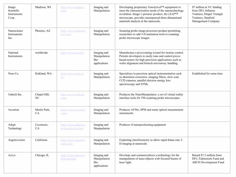
Imago Scientific Instruments Corp.
Madison, WI http://www.imago.com/#
Imaging and Manipulation
Developing proprietary Nanolytical™ equipment to meet the characterization needs of the nanotechnology revolution. Imago’s premier product, the LEAP™microscope, provides unsurpassed three-dimensional materials analysis at the nanoscale.
$7 million in VC funding from DFJ, InfineonVentures, Draper Triangle Ventures, Stanford Management Company
NanoscienceInstruments Inc.
Phoenix, AZ http://www.nanoscience.com/
Imaging and Manipulation
Scanning probe image processor product permitting researchers to add 3-D animation tools to scanning probe microscope images.
National Instruments
worldwide http://www.ni.com/ Imaging and ManipulationBio applications
Manufacture a piezo tuning wizard for motion control. Permits developers to easily tune and control piezo-based motors for high-precision applications such as wafer alignment and biotech microarray handling.
Nion Co. Kirkland, WA http://www.nion.com/
Imaging and Manipulation
Specializes in precision optical instrumentation such as aberration correctors, imaging filters, slow scan CCD cameras, parallel electron energy loss spectroscopy and STMs.
Established for some time
3rdtech Inc. Chapel Hill, NC
http://www.3rdtech.com/
Imaging and Manipulation
Produces the NanoManipulator, a set of virtual reality interface tools for TM scanning probe microscopes.
Accurion Menlo Park, CA
http://www.accurion.com/
Imaging and Manipulation
Produces AFMs, SPM and some optical measurement instruments
Adept Technology
Livermore, CA
http://www.adept.com/main/index.html
Imaging and Manipulation
Producer of nanopositioning equipment
Angstrovision California http://www.angstrovision.com/
Imaging and Manipulation
Exploiting interferometry to allow rapid-frame-rate 3-D imaging at nanoscale.
Arryx Chicago, IL http://www.arryx.com/home.html
Imaging and ManipulationBio applications
Develops and commercializes a technology for the manipulation of nano-objects with focused beams of laser light.
Raised $7.2 million from DFJ, Fahnestock Fund and ARCH Development Fund
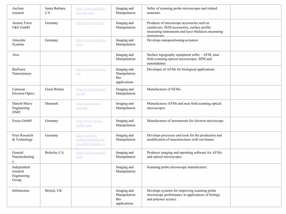
Asylum research
Santa Barbara, CA
http://www.asylumresearch.com/
Imaging and Manipulation
Seller of scanning probe microscopes and related materials.
Atomic Force F&E GmbH
Germany http://www.af-fe.de/ Imaging and Manipulation
Producer of microscope accessories such as cantilevers, SEM accessories, surface profile measuring instruments and layer thickness measuring instruments.
AttocubeSystems
Germany http://www.attocube.com/
Imaging and Manipulation
Develops nanopositioning actuators
Atos Imaging and Manipulation
Surface topography equipment seller – AFM, near field scanning optical microscopes, SPM and nanoindenter.
BioForceNanosciences
www.bioforcenano.com
Imaging and ManipulationBio applications
Developer of AFMs for biological applications.
CamscanElectron Optics
Great Britain http://www.camscan.co.uk/
Imaging and Manipulation
Manufacturer of SEMs.
Danish Micro Engineering DME
Denmark http://www.dme-spm.dk/
Imaging and Manipulation
Manufactures AFMs and near field scanning optical microscopes.
Focus GmbH Germany http://www.focus-gmbh.com/
Imaging and Manipulation
Manufacturer of instruments for electron microscopy.
Fries Research & Technology
Germany http://www.frt -gmbh.com/home/home.php3?sprache=uk
Imaging and Manipulation
Develops processes and tools for the production and modification of nanostructures with ion beams.
General Nanotechnology
Berkeley CA http://www.gennano.com/
Imaging and Manipulation
Produces imaging and operating software for AFMsand optical microscopes.
Independent research Engineering Group
Imaging and Manipulation
Scanning probe microscope manufacturer.
Infinitesima Bristol, UK Imaging and ManipulationBio applications
Develops systems for improving scanning probe microscope performance in applications of biology and polymer science.
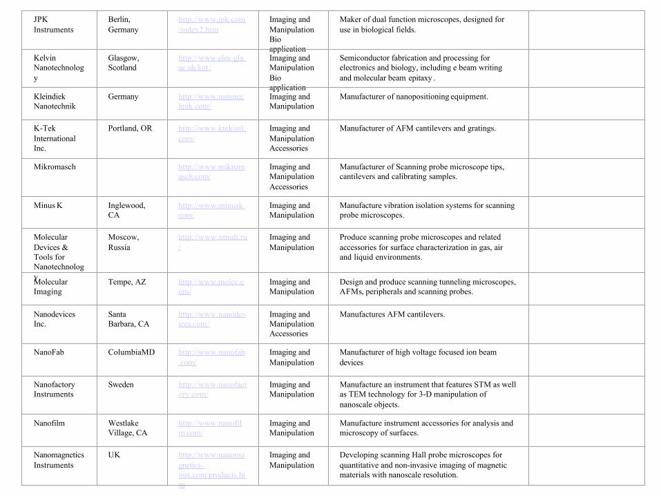
JPK Instruments
Berlin, Germany
http://www.jpk.com/index2.htm
Imaging and ManipulationBio application
Maker of dual function microscopes, designed for use in biological fields.
Kelvin Nanotechnology
Glasgow, Scotland
http://www.elec.gla.ac.uk/knt/
Imaging and ManipulationBio application
Semiconductor fabrication and processing for electronics and biology, including e beam writing and molecular beam epitaxy .
KleindiekNanotechnik
Germany http://www.nanotechnik.com/
Imaging and Manipulation
Manufacturer of nanopositioning equipment.
K-TekInternational Inc.
Portland, OR http://www.ktekintl.com/
Imaging and ManipulationAccessories
Manufacturer of AFM cantilevers and gratings.
Mikromasch http://www.mikromasch.com/
Imaging and ManipulationAccessories
Manufacturer of Scanning probe microscope tips, cantilevers and calibrating samples.
Minus K Inglewood, CA
http://www.minusk.com/
Imaging and Manipulation
Manufacture vibration isolation systems for scanning probe microscopes.
Molecular Devices & Tools for Nanotechnology
Moscow, Russia
http://www.ntmdt.ru/
Imaging and Manipulation
Produce scanning probe microscopes and related accessories for surface characterization in gas, air and liquid environments.
Molecular Imaging
Tempe, AZ http://www.molec.com/
Imaging and Manipulation
Design and produce scanning tunneling microscopes, AFMs, peripherals and scanning probes.
NanodevicesInc.
Santa Barbara, CA
http://www.nanodevices.com/
Imaging and ManipulationAccessories
Manufactures AFM cantilevers.
NanoFab ColumbiaMD http://www.nanofab.com/
Imaging and Manipulation
Manufacturer of high voltage focused ion beam devices
NanofactoryInstruments
Sweden http://www.nanofactory.com/
Imaging and Manipulation
Manufacture an instrument that features STM as well as TEM technology for 3-D manipulation of nanoscale objects.
Nanofilm Westlake Village, CA
http://www.nanofilm.com/
Imaging and Manipulation
Manufacture instrument accessories for analysis and microscopy of surfaces.
NanomagneticsInstruments
UK http://www.nanomagnetics-inst.com/products.htm
Imaging and Manipulation
Developing scanning Hall probe microscopes for quantitative and non-invasive imaging of magnetic materials with nanoscale resolution.
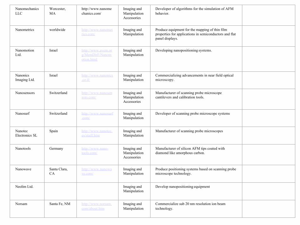
NanomechanicsLLC
Worcester, MA
http://www.nanomechanics.com/
Imaging and ManipulationAccessories
Developer of algorithms for the simulation of AFM behavior.
Nanometrics worldwide http://www.nanometrics.com/
Imaging and Manipulation
Produce equipment for the mapping of thin film properties for applications in semiconductors and flat panel displays.
NanomotionLtd.
Israel http://www.avem.org/MemDirF/Nanomotion.html
Imaging and Manipulation
Developing nanopositioning systems.
NanonicsImaging Ltd.
Israel http://www.nanonics.co.il/
Imaging and Manipulation
Commercializing advancements in near field optical microscopy.
Nanosensors Switzerland http://www.nanosensors.com/
Imaging and ManipulationAccessories
Manufacturer of scanning probe microscope cantilevers and calibration tools.
Nanosurf Switzerland http://www.nanosurf.com/
Imaging and Manipulation
Developer of scanning probe microscope systems
NanotecElectronics SL
Spain http://www.nanotec.es/staff.htm
Imaging and Manipulation
Manufacturer of scanning probe microscopes
Nanotools Germany http://www.nano-tools.com/
Imaging and ManipulationAccessories
Manufacturer of silicon AFM tips coated with diamond like amorphous carbon.
Nanowave Santa Clara, CA
http://www.nanowave.com/
Imaging and Manipulation
Produce positioning systems based on scanning probe microscope technology.
Neolim Ltd. Imaging and Manipulation
Develop nanopositioning equipment
Norsam Santa Fe, NM http://www.norsam.com/about.htm
Imaging and Manipulation
Commercialize sub 20 nm resolution ion beam technology.

Omicron Germany http://www.omicron-instruments.com/
Imaging and Manipulation
Manufacturer of scanning tunneling microscopes.
Orsay Physics France http://www.orsayphysics.com/
Imaging and Manipulation
Producer of focused ion beam columns in partnership with LEO.
Pacific Nanotechnology Inc.
Santa Clara, CA
http://www.pacificnanotech.com/
Imaging and Manipulation
High performance inexpensive AFM with intuitive imaging capabilities.
Physical Electronics Inc.
Germany http://www.phi.com/ Imaging and Manipulation
Manufacture a variety of surface science instruments.
Piezomax(nownPoint)
Madison, WI http://www.piezomax.com/
Imaging and Manipulation
Manufacture scanning probe tips and nanopositioningdevices.
PSIA Korea http://www.psia.co.kr/
Imaging and ManipulationAccessories
Manufacture SPMs and cantilevers.
Queensgate Imaging and Manipulation
Manufacturer of nanopositioning systems.
QuesantInstruments Corp.
worldwide http://www.quesant.com/
Imaging and Manipulation
Manufacturer of scanning probe microscopes.
RHK Technology
Troy, MI http://www.rhk-tech.com/
Imaging and Manipulation
Manufacturer of UHV AFM/STM systems for molecular imaging.
Surface Imaging Systems
Germany http://www.sis-gmbh.com/
Imaging and Manipulation
Manufacturer of scanning probe microscope peripherals.
Triple-O Microscopy
Germany http://www.triple-o.de/Triple-O.Microscopy.html
Imaging and Manipulation
Manufacturer of SPM.
Visitec Germany http://www.visitec-em.de/
Imaging and Manipulation
Very large chamber SEM producer.
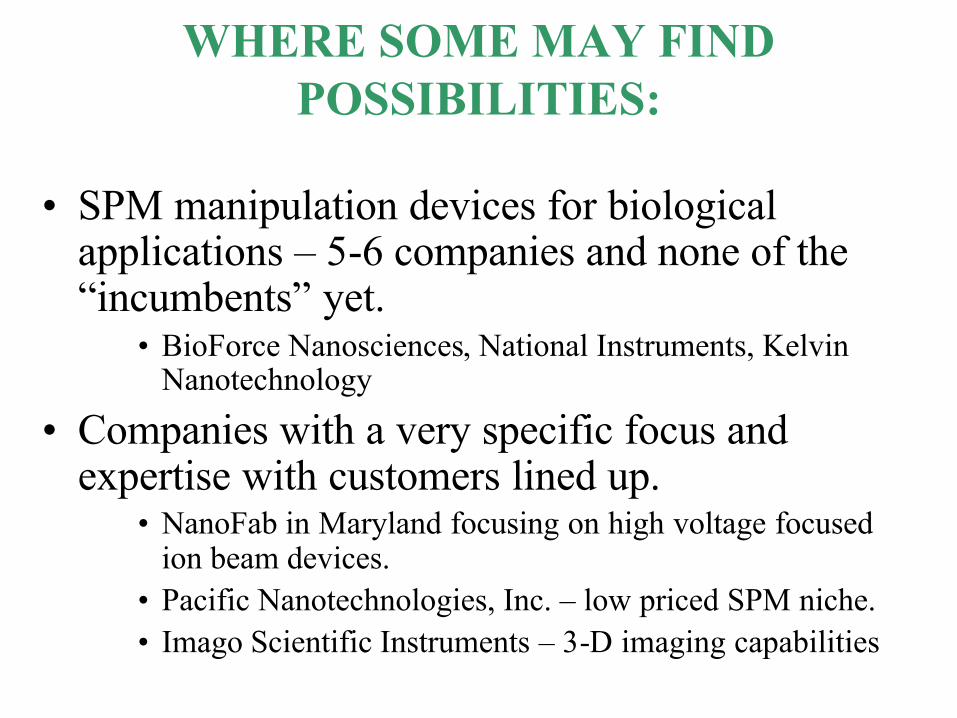
WHERE SOME MAY FIND POSSIBILITIES:
• SPM manipulation devices for biological applications – 5-6 companies and none of the “incumbents” yet.
• BioForce Nanosciences, National Instruments, Kelvin Nanotechnology
• Companies with a very specific focus and expertise with customers lined up.
• NanoFab in Maryland focusing on high voltage focused ion beam devices.
• Pacific Nanotechnologies, Inc. – low priced SPM niche.• Imago Scientific Instruments – 3-D imaging capabilities
EXCITING POSSIBILITIES:
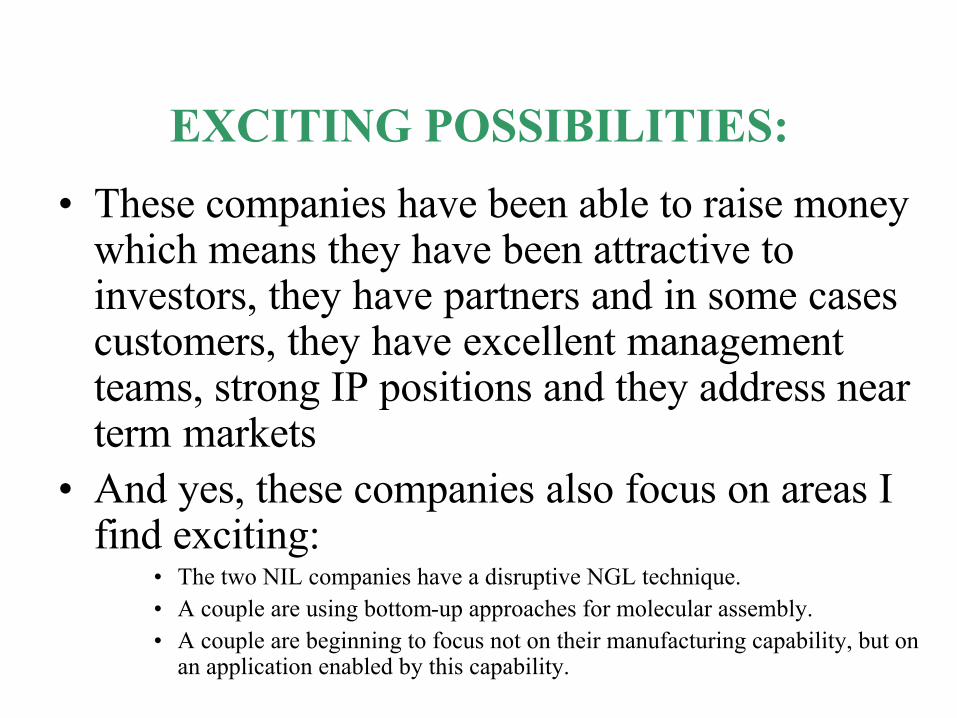
EXCITING POSSIBILITIES:
• These companies have been able to raise money which means they have been attractive to investors, they have partners and in some cases customers, they have excellent management teams, strong IP positions and they address near term markets
• And yes, these companies also focus on areas I find exciting:
• The two NIL companies have a disruptive NGL technique.• A couple are using bottom-up approaches for molecular assembly.• A couple are beginning to focus not on their manufacturing capability, but on
an application enabled by this capability.

EXCITING POSSIBILITIES:• Molecular Imprints
NanoImprint Lithography systems called Step and Flash Imprint Lithography, developed at Univ. of Texas based on embossing.
Technique uses a quartz template with a circuit pattern etched into it. The quartz surface, covered with a release layer, is gently pressed into a thin layer of low viscosity, silicon containing monomer that upon illumination by a UV lamp is polymerized into a hard material. When the quartz template is removed, the pattern is left on the surface.
Thoughts:• NIL is a disruptive NGL. If they can find application niches that take
advantage of its strength, they can develop the technology to a point where it performs better than existing lithography techniques. They have a partner and a customer in Motorola.
• It is still top down manufacturing.• Still selling their manufacturing capability and not a higher value potential
application.
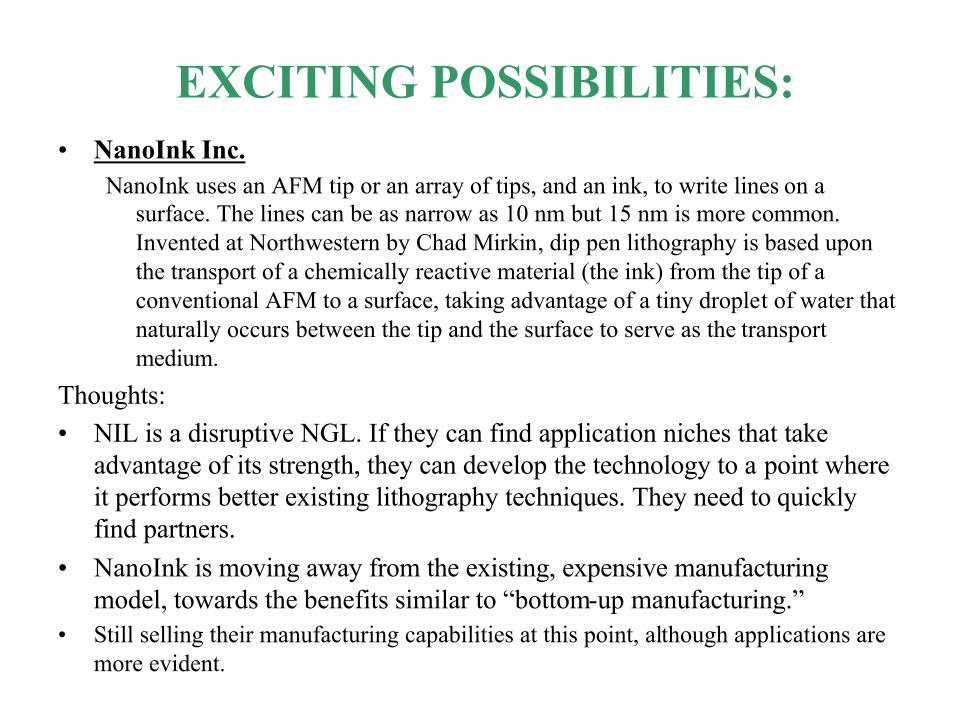
EXCITING POSSIBILITIES:• NanoInk Inc.
NanoInk uses an AFM tip or an array of tips, and an ink, to write lines on a surface. The lines can be as narrow as 10 nm but 15 nm is more common. Invented at Northwestern by Chad Mirkin, dip pen lithography is based upon the transport of a chemically reactive material (the ink) from the tip of a conventional AFM to a surface, taking advantage of a tiny droplet of water that naturally occurs between the tip and the surface to serve as the transport medium.
Thoughts:• NIL is a disruptive NGL. If they can find application niches that take
advantage of its strength, they can develop the technology to a point where it performs better existing lithography techniques. They need to quickly find partners.
• NanoInk is moving away from the existing, expensive manufacturing model, towards the benefits similar to “bottom-up manufacturing.”
• Still selling their manufacturing capabilities at this point, although applications are more evident.
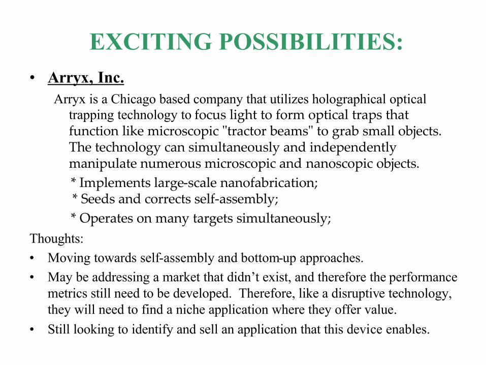
EXCITING POSSIBILITIES:• Arryx, Inc.
Arryx is a Chicago based company that utilizes holographical optical trapping technology to focus light to form optical traps that function like microscopic "tractor beams" to grab small objects.The technology can simultaneously and independently manipulate numerous microscopic and nanoscopic objects.* Implements large-scale nanofabrication;* Seeds and corrects self-assembly;* Operates on many targets simultaneously;
Thoughts: • Moving towards self-assembly and bottom-up approaches.• May be addressing a market that didn’t exist, and therefore the performance
metrics still need to be developed. Therefore, like a disruptive technology, they will need to find a niche application where they offer value.
• Still looking to identify and sell an application that this device enables.
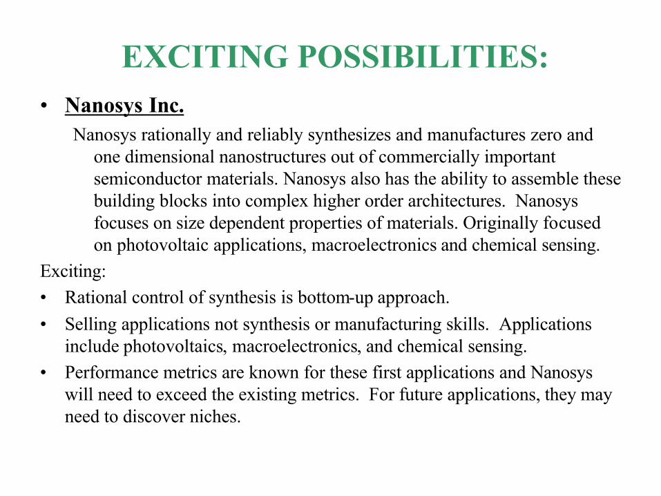
EXCITING POSSIBILITIES:• Nanosys Inc.
Nanosys rationally and reliably synthesizes and manufactures zero and one dimensional nanostructures out of commercially important semiconductor materials. Nanosys also has the ability to assemble these building blocks into complex higher order architectures. Nanosysfocuses on size dependent properties of materials. Originally focused on photovoltaic applications, macroelectronics and chemical sensing.
Exciting: • Rational control of synthesis is bottom-up approach.• Selling applications not synthesis or manufacturing skills. Applications
include photovoltaics, macroelectronics, and chemical sensing. • Performance metrics are known for these first applications and Nanosys
will need to exceed the existing metrics. For future applications, they may need to discover niches.
REVISITING THE FRAMEWORK FOR INVESTMENT OPPORTUNITIES:
• Source of a Visual Picture for Strategy Purposes:– Found some nanoimprint lithography techniques that may be disruptive.
Found a lot of “tool” companies trying to compete against the incumbents with sustaining technologies.
– Most technologies are still “top-down” manufacturing processes, that don’t fully take advantage of the opportunities that will some day be enabled at the nanoscale. A bit early for “bottom-up” promises.
– Great companies are selling applications (Nanosys, NanoGram Devices)
• The excitement for nanotech tools may be leading us to capital market myopia.
• Good due diligence is critical as this field has matured quickly. There is significant intellectual property and plenty of companies that are already in business.
REVISITING INVESTMENT OPPORTUNITIES:WHAT DID WE LEARN?
• What is the market?• Deutsche Bank reports a $13 billion market in 2001 for ultra-
precision technology…• Analytical Instruments Industry Report puts SPM market at $150-170
million in 2001, with expectations to double…• Veeco – 2002 sales @ $298.9 million down from $449 million in
2001. Metrology (AFMs) at $152 million. Process equipment (etch and deposition products) at $146 million. Veeco is often held up as the leader.
• Lesson:• Market isn’t that large yet, and had a hiccup recently.• Need to better understand how the market functions at this point.
REVISITING INVESTMENT OPPORTUNITIES:WHAT DID WE LEARN?
• Back to Clayton Christensen and “sustaining” vs. “disruptive” technologies.
• I’d posit that my survey has shown most of the technologies to be sustaining. To penetrate the market you will have to be better than the existing technology in almost every measurable metric. I think that improvements in SEMs, TEMs, SPM, and many of the enhanced manipulation devices will be sustaining. The “Big Boys” are well positioned, and history has shown that the leading practitioners of the original technology, lead in new sustaining technologies.
• The SPM market, especially, is fairly mature, and I don’t believe there are many high value investment returns in this area. There are some fantastic improvements (such as imaging speed increases and 3-D imaging) on the horizon, but I think that the best technology transfer approach would be a licensing model.
REVISITING INVESTMENT OPPORTUNITIES:WHAT DID WE LEARN?
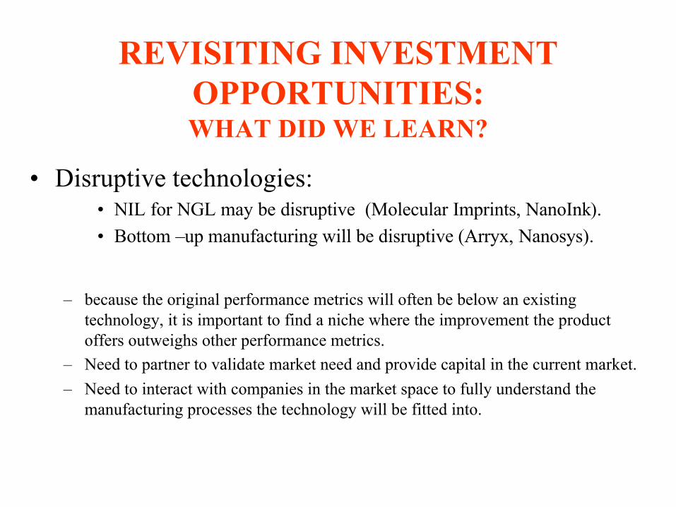
• Disruptive technologies:• NIL for NGL may be disruptive (Molecular Imprints, NanoInk). • Bottom –up manufacturing will be disruptive (Arryx, Nanosys).
– because the original performance metrics will often be below an existing technology, it is important to find a niche where the improvement the product offers outweighs other performance metrics.
– Need to partner to validate market need and provide capital in the current market.– Need to interact with companies in the market space to fully understand the
manufacturing processes the technology will be fitted into.
CONCLUSION:
• The opportunities for specialized firms in nanomanufacturing – what they will need.
• The opportunities for a firm such as Harris & Harris Group, Inc.
• Strategies and rules are often designed to then be broken or proven incorrect. However, then at least one has been conscious of the process and knows what one is getting into.
CONCLUSION:
• There are, and there will continue to be some exciting opportunities in the tools sector of nanomanufacturing. However, I believe that most of these will be sustaining technologies, and the incumbent firms will be best able to profit from them. Investors pursuing start-ups within this space have two major challenges.– Management must have proven industry experience in this market space
and have relationships with their ultimate customers.– Investment teams should be focused in this area with operating expertise
coming from these industries. I don’t believe the ultimate returns will be as high as application based nanotechnology improvements, and therefore they must have the skill set to attempt to reduce the risks.
– If the team doesn’t have this expertise, I believe a licensing model may be the most effective means to get a return on the technology.
– No room for error in execution
CONCLUSION:
• As you probably can tell, Harris & Harris Group tends to be a traditional early stage investor that looks to maintain a well diversified portfolio investing in large market opportunities. We look at each opportunity on its own merits, and therefore it is difficult to make generalizations, but in nanomanufacturing and in nanotechnology in general, we would focus on the following:– All the traditional strengths investors expect.– Companies focused on high value applications rather than tools in
large markets.– Bottom-up manufacturing and other properties that take advantage of
capabilities specific to the nanoscale.– Room to fumble finding the ultimate niche, as this technology is early
stage.