welcome to svecw
TRANSCRIPT

SHRI VISHNU ENGINEERING COLLEGE FOR WOMEN::BHIMAVARAM
DEPARTMENT OF INFORMATION TECHNOLOGY
Computer Organization and Architecture Lecture Notes

UNIT-1
DEPARTMENT OF INFORMATION TECHNOLOGY::SVECW Page 1
UNIT-1
A BRIEF HISTORY OF COMPUERS: We begin our study of computers with a brief history.
First Generation: Vacuum Tubes
ENIAC The ENIAC (Electronic Numerical Integrator And Computer), designed and constructed at
the University of Pennsylvania, was the world’s first general-purpose electronic digital computer.
The project was a response to U.S needs during World War II.
John Mauchly, a professor of electrical engineering at the University of Pennsylvania, and
John Eckert, one of his graduate students, proposed to build a general-purpose computer using
vacuum tubes for the BRL’s application. In 1943, the Army accepted this proposal, and work began
on the ENIAC. The resulting machine was enormous, weighing 30 tons, occupying 1500 square feet
of floor space, and containing more than 18,000 vacuum tubes. When operating, it consumed 140
kilowatts of power. It was also substantially faster than any electromechanical computer, capable of
5000 additions per second.
The ENIAC was completed in 1946, too late to be used in the war effort. The use of the ENIAC
for a purpose other than that for which it was built demonstrated its general-purpose nature. The
ENIAC continued to operate under BRL management until 1955, when it was disassembled.
THE VON NEUMANN MACHINE The task of entering and altering programs for the ENIAC was
extremely tedious. The programming process can be easy if the program could be represented in a
form suitable for storing in memory alongside the data. Then, a computer could get its instructions
by reading them from memory, and a program could be set or altered by setting the values of a
portion of memory. This idea is known as the stored-program concept. The first publication of the
idea was in a 1945 proposal by von Neumann for a new computer, the EDVAC (Electronic Discrete
Variable Computer).
In 1946, von Neumann and his colleagues began the design of a new stored-program
computer, referred to as the IAS computer, at the Princeton Institute for Advanced Studies. The IAS
computer,although not completed until 1952,is the prototype of all subsequent general-purpose
computers.
Figure 1.1 Structure of IAS Computer

UNIT-1
DEPARTMENT OF INFORMATION TECHNOLOGY::SVECW Page 2
Figure 1.1 shows the general structure of the IAS computer). It consists of
A main memory, which stores both data and instruction
An arithmetic and logic unit (ALU) capable of operating on binary data
A control unit, which interprets the instructions in memory and causes them to be executed
Input and output (I/O) equipment operated by the control unit
This structure was outlined in von Neumann’s earlier proposal, which is worth quoting at this
point:
First: Because the device is primarily a computer, it will have to perform the elementary operations
of arithmetic most frequently. At any rate a central arithmetical part of the device will probably
have to exist and this constitutes the first specific part: CA.
Second: The logical control of the device, that is, the proper sequencing of its operations, can be
most efficiently carried out by a central control organ. By the central control and the organs which
perform it form the second specific part: CC
Third: Any device which is to carry out long and complicated sequences of operations (specifically
of calculations) must have a considerable memory . . . At any rate, the total memory constitutes the
third specific part of the device: M.
Fourth: The device must have organs to transfer . . . information from R into its specific parts C and
M. These organs form its input, the fourth specific part: I
Fifth: The device must have organs to transfer . . . from its specific parts C and M into R. These
organs form its output, the fifth specific part: O.
The control unit operates the IAS by fetching instructions from memory and executing them one at
a time. A more detailed structure diagram is shown in Figure 1.2. This figure reveals that both the
control unit and the ALU contain storage locations, called registers, defined as follows:
• Memory buffer register (MBR): Contains a word to be stored in memory or sent to the I/O
unit, or is used to receive a word from memory or from the I/O unit.
• Memory address register (MAR): Specifies the address in memory of the word to be
written from or read into the MBR.
• Instruction register (IR): Contains the 8-bit opcode instruction being executed.
• Instruction buffer register (IBR): Employed to hold temporarily the right-hand instruction
from a word in memory.
• Program counter (PC): Contains the address of the next instruction-pair to be fetched from
memory.
• Accumulator (AC) and multiplier quotient (MQ): Employed to hold temporarily operands
and results of ALU operations.

UNIT-1
DEPARTMENT OF INFORMATION TECHNOLOGY::SVECW Page 3
Figure 1.2 Expanded Structure of IAS Computer
COMMERCIAL COMPUTERS The 1950s saw the birth of the computer industry with two
companies, Sperry and IBM, dominating the marketplace. In 1947, Eckert and Mauchly formed the
Eckert-Mauchly Computer Corporation to manufacture computers commercially. Their first
successful machine was the UNIVAC I (Universal Automatic Computer), which was commissioned
by the Bureau of the Census for the 1950 calculations.The Eckert-Mauchly Computer Corporation
became part of the UNIVAC division of Sperry-Rand Corporation, which went on to build a series of
successor machines.
The UNIVAC I was the first successful commercial computer. It was intended for both
scientific and commercial applications.
The UNIVAC II, which had greater memory capacity and higher performance than the
UNIVAC I, was delivered in the late 1950s and illustrates several trends that have remained
characteristic of the computer industry.
The UNIVAC division also began development of the 1100 series of computers, which was to
be its major source of revenue. This series illustrates a distinction that existed at one time. The first
model, the UNIVAC 1103, and its successors for many years were primarily intended for scientific
applications, involving long and complex calculations.

UNIT-1
DEPARTMENT OF INFORMATION TECHNOLOGY::SVECW Page 4
The Second Generation: Transistors
The first major change in the electronic computer came with the replacement of the vacuum
tube by the transistor. The transistor is smaller, cheaper, and dissipates less heat than a vacuum
tube but can be used in the same way as a vacuum tube to construct computers. Unlike the vacuum
tube, which requires wires, metal plates, a glass capsule, and a vacuum, the transistor is a solid-
state device, made from silicon.
The transistor was invented at Bell Labs in 1947 and by the 1950s had launched an
electronic revolution. It was not until the late 1950s, however, that fully transistorized computers
were commercially available.
The use of the transistor defines the second generation of computers. It has become widely
accepted to classify computers into generations based on the fundamental hardware technology
employed (Table 1.1).
Table 1.1 Computer Generations
THE IBM 7094 From the introduction of the 700 series in 1952 to the introduction of the last
member of the 7000 series in 1964, this IBM product line underwent an evolution that is typical of
computer products. Successive members of the product line show increased performance,
increased capacity, and/or lower cost.
The Third Generation: Integrated Circuits
In 1958 came the achievement that revolutionized electronics and started the era of
microelectronics: the invention of the integrated circuit. It is the integrated circuit that defines the
third generation of computers.
MICROELECTRONICS: Microelectronics means, literally, “small electronics.” Since the beginnings
of digital electronics and the computer industry, there has been a persistent and consistent trend
toward the reduction in size of digital electronic circuits.
IBM SYSTEM/360 By 1964, IBM had a firm grip on the computer market with its 7000 series of
machines. In that year, IBM announced the System/360, a new family of computer products.
DEC PDP-8 In the same year that IBM shipped its first System/360, another momentous first
shipment occurred: PDP-8 from Digital Equipment Corporation (DEC).At a time when the average
computer required an air-conditioned room,the PDP-8 (dubbed a minicomputer by the industry,
after the miniskirt of the day) was small enough that it could be placed on top of a lab bench or be
built into other equipment. It could not do everything the mainframe could, but at $16,000, it was
cheap enough for each lab technician to have one. In contrast, the System/360 series of mainframe
computers introduced just a few months before cost hundreds of thousands of dollars.

UNIT-1
DEPARTMENT OF INFORMATION TECHNOLOGY::SVECW Page 5
Later Generations
Table 1.1 suggests that there have been a number of later generations, based on advances in
integrated circuit technology. With the introduction of large-scale integration (LSI), more than
1000 components can be placed on a single integrated circuit chip. Very-large-scale integration
(VLSI) achieved more than 10,000 components per chip, while current ultra-large-scale integration
(ULSI) chips can contain more than one million components.
SEMICONDUCTOR MEMORY The first application of integrated circuit technology to computers
was construction of the processor (the control unit and the arithmetic and logic unit) out of
integrated circuit chips. But it was also found that this same technology could be used to construct
memories.
MICROPROCESSORS Just as the density of elements on memory chips has continued to rise,so has
the density of elements on processor chips.As time went on,more and more elements were placed
on each chip, so that fewer and fewer chips were needed to construct a single computer processor.
A breakthrough was achieved in 1971,when Intel developed its 4004.The 4004 was the
first chip to contain all of the components of a CPU on a single chip.
The next major step in the evolution of the microprocessor was the introduction in 1972 of
the Intel 8008. This was the first 8-bit microprocessor and was almost twice as complex as the
4004.
Neither of these steps was to have the impact of the next major event: the introduction in
1974 of the Intel 8080.This was the first general-purpose microprocessor. Whereas the 4004 and
the 8008 had been designed for specific applications, the 8080 was designed to be the CPU of a
general-purpose microcomputer
About the same time, 16-bit microprocessors began to be developed. However, it was not
until the end of the 1970s that powerful, general-purpose 16-bit microprocessors appeared. One of
these was the 8086.
DESIGNING FOR PERFORMANCE
Year by year, the cost of computer systems continues to drop dramatically, while the
performance and capacity of those systems continue to rise equally dramatically. Desktop
applications that require the great power of today’s microprocessor-based systems include
• Image processing
• Speech recognition
• Videoconferencing
• Multimedia authoring
• Voice and video annotation of files
• Simulation modeling
Microprocessor Speed
The evolution of Microprocessors continues to bear out Moore’s law. So long as this law holds,
chipmakers can unleash a new generation of chips every three years—with four times as many
transistors. In microprocessors, the addition of new circuits, and the speed boost that comes from
reducing the distances between them, has improved performance four- or fivefold every three

UNIT-1
DEPARTMENT OF INFORMATION TECHNOLOGY::SVECW Page 6
years or so since Intel launched its x86 family in 1978. The more elaborate techniques for feeding
the monster into contemporary processors are the following:
• Branch prediction: The processor looks ahead in the instruction code fetched from
memory and predicts which branches, or groups of instructions, are likely to be processed next
• Data flow analysis: The processor analyzes which instructions are dependent on each
other’s results, or data, to create an optimized schedule of instructions
• Speculative execution: Using branch prediction and data flow analysis, some processors
speculatively execute instructions ahead of their actual appearance in the program execution,
holding the results in temporary locations.
Performance Balance
While processor power has raced ahead at breakneck speed, other critical components of
the computer have not kept up.The result is a need to look for performance balance: an adjusting of
the organization and architecture to compensate for the mismatch among the capabilities of the
various components.
The interface between processor and main memory is the most crucial pathway in the entire
computer because it is responsible for carrying a constant flow of program instructions and data
between memory chips and the processor.
There are a number of ways that a system architect can attack this problem, all of which are
reflected in contemporary computer designs. Consider the following examples:
• Increase the number of bits that are retrieved at one time by making DRAMs “wider” rather
than “deeper” and by using wide bus data paths.
• Change the DRAM interface to make it more efficient by including a cache7 or other
buffering scheme on the DRAM chip.
• Reduce the frequency of memory access by incorporating increasingly complex and efficient
cache structures between the processor and main memory.
• Increase the interconnect bandwidth between processors and memory by using higher-
speed buses and by using a hierarchy of buses to buffer and structure data flow.
Improvements in Chip Organization and Architecture
There are three approaches to achieving increased processor speed:
• Increase the hardware speed of the processor.
• Increase the size and speed of caches that are interposed between the processor and main
memory. In particular, by dedicating a portion of the processor chip itself to the cache, cache access
times drop significantly.
• Make changes to the processor organization and architecture that increase the effective
speed of instruction execution.
However, as clock speed and logic density increase, a number of obstacles become more
significant:
• Power: As the density of logic and the clock speed on a chip increase, so does the power
density.

UNIT-1
DEPARTMENT OF INFORMATION TECHNOLOGY::SVECW Page 7
• RC delay: The speed at which electrons can flow on a chip between transistors is limited by
the resistance and capacitance of the metal wires connecting them; specifically, delay increases as
the RC product increases. As components on the chip decrease in size, the wire interconnects
become thinner, increasing resistance. Also, the wires are closer together, increasing capacitance.
• Memory latency: Memory speeds lag processor speeds.
Beginning in the late 1980s, and continuing for about 15 years, two main strategies have been
used to increase performance beyond what can be achieved simply by increasing clock speed. First,
there has been an increase in cache capacity. Second, the instruction execution logic within a
processor has become increasingly complex to enable parallel execution of instructions within the
processor.
Two noteworthy design approaches have been pipelining and superscalar. A pipeline works
much as an assembly line in a manufacturing plant enabling different stages of execution of
different instructions to occur at the same time along the pipeline. A superscalar approach in
essence allows multiple pipelines within a single processor so that instructions that do not depend
on one another can be executed in parallel.
EVOLUTION OF INTEL X86 ARCHITECTURE:
We have Two computer families: the Intel x86 and the ARM architecture. The current x86
offerings represent the results of decades of design effort on complex instruction set computers
(CISCs).
The x86 incorporates the sophisticated design principles once found only on mainframes and
supercomputers and serves as an excellent example of CISC design. An alternative approach to
processor design in the reduced instruction set computer (RISC). The ARM architecture is used in a
wide variety of embedded systems and is one of the most powerful and best-designed RISC-based
systems on the market.
In terms of market share, Intel has ranked as the number one maker of microprocessors for
non-embedded systems for decades, a position it seems unlikely to yield. Interestingly, as
microprocessors have grown faster and much more complex, Intel has actually picked up the pace.
Intel used to develop microprocessors one after another, every four years.
It is worthwhile to list some of the highlights of the evolution of the Intel product line:
• 8080: The world’s first general-purpose microprocessor. This was an 8-bit machine, with an
8-bit data path to memory. The 8080 was used in the first personal computer, the Altair.
• 8086: A far more powerful, 16-bit machine. In addition to a wider data path and larger
registers, the 8086 sported an instruction cache, or queue, that prefetches a few instructions before
they are executed. A variant of this processor, the 8088, was used in IBM’s first personal computer,
securing the success of Intel. The 8086 is the first appearance of the x86 architecture.
• 80286: This extension of the 8086 enabled addressing a 16-MByte memory instead of just 1
MByte.
• 80386: Intel’s first 32-bit machine, and a major overhaul of the product. With a 32-bit

UNIT-1
DEPARTMENT OF INFORMATION TECHNOLOGY::SVECW Page 8
architecture, the 80386 rivaled the complexity and power of minicomputers and mainframes
introduced just a few years earlier. This was the first Intel processor to support multitasking,
meaning it could run multiple programs at the same time.
• 80486: The 80486 introduced the use of much more sophisticated and powerful cache
technology and sophisticated instruction pipelining. The 80486 also offered a built-in math
coprocessor, offloading complex math operations from the main CPU.
• Pentium: With the Pentium, Intel introduced the use of superscalar techniques, which allow
multiple instructions to execute in parallel.
• Pentium Pro: The Pentium Pro continued the move into superscalar organization begun
with the Pentium, with aggressive use of register renaming, branch prediction, data flow analysis,
and speculative execution.
• Pentium II: The Pentium II incorporated Intel MMX technology, which is designed
specifically to process video, audio, and graphics data efficiently.
• Pentium III: The Pentium III incorporates additional floating-point instructions to support
3D graphics software.
• Pentium 4: The Pentium 4 includes additional floating-point and other enhancements for
multimedia.8
• Core: This is the first Intel x86 microprocessor with a dual core, referring to the
implementation of two processors on a single chip.
• Core 2: The Core 2 extends the architecture to 64 bits. The Core 2 Quad provides four
processors on a single chip.
Over 30 years after its introduction in 1978, the x86 architecture continues to dominate the
processor market outside of embedded systems. Although the organization and technology of the
x86 machines has changed dramatically over the decades, the instruction set architecture has
evolved to remain backward compatible with earlier versions. Thus, any program written on an
older version of the x86 architecture can execute on newer versions. All changes to the instruction
set architecture have involved additions to the instruction set, with no subtractions. The rate of
change has been the addition of roughly one instruction per month added to the architecture over
the 30 years. so that there are now over 500 instructions in the instruction set.
The x86 provides an excellent illustration of the advances in computer hardware over the
past 30 years. The 1978 8086 was introduced with a clock speed of 5 MHz and had 29,000
transistors. A quad-core Intel Core 2 introduced in 2008 operates at 3 GHz, a speedup of a factor of
600, and has 820 million transistors, about 28,000 times as many as the 8086. Yet the Core 2 is in
only a slightly larger package than the 8086 and has a comparable cost.
COMPUTER COMPONENTS
Virtually all contemporary computer designs are based on concepts developed by John von
Neumann at the Institute for Advanced Studies, Princeton. Such a design is referred to as the von
Neumann architecture and is based on three key concepts:
• Data and instructions are stored in a single read–write memory.

UNIT-1
DEPARTMENT OF INFORMATION TECHNOLOGY::SVECW Page 9
• The contents of this memory are addressable by location, without regard to the type of data
contained there.
• Execution occurs in a sequential fashion (unless explicitly modified) from one instruction to
the next.
If there is a particular computation to be performed, a configuration of logic components
designed specifically for that computation could be constructed. The resulting “program” is in the
form of hardware and is termed a hardwired program.
Now consider this alternative. Suppose we construct a general-purpose configuration of
arithmetic and logic functions. This set of hardware will perform various functions on data
depending on control signals applied to the hardware. In the original case of customized hardware,
the system accepts data and produces results (Figure 1.3a). With general-purpose hardware, the
system accepts data and control signals and produces results.
Thus, instead of rewiring the hardware for each new program, the programmer merely needs
to supply a new set of control signals by providing a unique code for each possible set of control
signals, and let us add to the general-purpose hardware a segment that can accept a code and gen-
erate control signals (Figure 1.3b). To distinguish this new method of programming, a sequence of
codes or instructions is called software.
1.3 Hardware and Software approaches
Figure 1.3b indicates two major components of the system: an instruction interpreter and a
module of general-purpose arithmetic and logic functions.These two constitute the CPU. Data and
instructions must be put into the system. For this we need some sort of input module. A means of
reporting results is needed, and this is in the form of an output module. Taken together, these are
referred to as I/O components.

UNIT-1
DEPARTMENT OF INFORMATION TECHNOLOGY::SVECW Page 10
There must be a place to store temporarily both instructions and data. That module is called
memory, or main memory to distinguish it from external storage or peripheral devices. Von
Neumann pointed out that the same memory could be used to store both instructions and data.
Figure 1.4 illustrates these top-level components and suggests the interactions among them.
The CPU exchanges data with memory. For this purpose, it typically makes use of two internal (to
the CPU) registers: a memory address register (MAR), which specifies the address in memory for
the next read or write, and a memory buffer register (MBR), which contains the data to be written
into memory or receives the data read from memory. Similarly, an I/O address register (I/OAR)
specifies a particular I/O device. An I/O buffer (I/OBR) register is used for the exchange of data
between an I/O module and the CPU.
A memory module consists of a set of locations, defined by sequentially numbered addresses.
Each location contains a binary number that can be interpreted as either an instruction or data. An
I/O module transfers data from external devices to CPU and memory, and vice versa. It contains
internal buffers for temporarily holding these data until they can be sent on.
1.4 Computer Components
COMPUTER FUNCTIONS
The basic function performed by a computer is execution of a program, which consists of a set of
instructions stored in memory. Instruction processing consists of two steps: The processor reads (
fetches) instructions from memory one at a time and executes each instruction. Program execution
consists of repeating the process of instruction fetch and instruction execution.
The processing required for a single instruction is called an instruction cycle. Using the
simplified two-step description given previously, the instruction cycle is depicted in Figure 1.5. The

UNIT-1
DEPARTMENT OF INFORMATION TECHNOLOGY::SVECW Page 11
two steps are referred to as the fetch cycle and the execute cycle. Program execution halts only if
the machine is turned off, some sort of unrecoverable error occurs, or a program instruction that
halts the computer is encountered.
Figure 1.5 Basic Instruction Cycle
Instruction Fetch and Execute
At the beginning of each instruction cycle, the processor fetches an instruction from
memory. The program counter (PC) holds the address of the instruction to be fetched next, the
processor always increments the PC after each instruction fetch so that it will fetch the next in-
struction in sequence.
For example, consider a computer in which each instruction occupies one 16-bit word of
memory. If the program counter is set to location 300. The processor will next fetch the instruction
at location 300. On next instruction cycles, it will fetch instructions from locations 301,302,303,and
so on.
The fetched instruction is loaded into a register in the processor known as the instruction
register (IR). The processor interprets the instruction and performs the required action. In general,
these actions fall into four categories:
• Processor-memory: Data may be transferred from processor to memory or from memory
to processor.
• Processor-I/O: Data may be transferred to or from a peripheral device by transferring
between the processor and an I/O module.
• Data processing: The processor may perform some arithmetic or logic operation on data.
• Control: An instruction may specify that the sequence of execution be altered. For example,
the processor may fetch an instruction from location 149, which specifies that the next instruction
be from location 182. The processor will remember this fact by setting the program counter to
182.Thus,on the next fetch cycle, the instruction will be fetched from location 182 rather than 150.
An instruction’s execution may involve a combination of these actions. Consider a simple
example using a hypothetical machine that includes the characteristics listed in Figure 1.6. The
processor contains a single data register, called an accumulator (AC). Both instructions and data are
16 bits long. Thus, it is convenient to organize memory using 16-bit words. The instruction format
provides 4 bits for the opcode, so that there can be as many as 24 = 16 different opcodes, and up to
212 = 4096 (4K) words of memory can be directly addressed.

UNIT-1
DEPARTMENT OF INFORMATION TECHNOLOGY::SVECW Page 12
Figure 1.6 Characteristics of a Hypothetical machine
Figure 1.7 illustrates a partial program execution, showing the relevant portions of memory
and processor registers.1 The program fragment shown adds the contents of the memory word at
address 940 to the contents of the memory word at address 941 and stores the result in later
location.
Figure 1.7 Example of Program Execution
Three instructions are required:
1. The PC contains 300, the address of the first instruction. This instruction (the value

UNIT-1
DEPARTMENT OF INFORMATION TECHNOLOGY::SVECW Page 13
1940 in hexadecimal) is loaded into the instruction register IR and the PC is incremented.
2. The first 4 bits (first hexadecimal digit) in the IR indicate that the AC is to be loaded.
The remaining 12 bits (three hexadecimal digits) specify the address (940) from which data are to
be loaded.
3. The next instruction (5941) is fetched from location 301 and the PC is incremented.
4. The old contents of the AC and the contents of location 941 are added and the result
is stored in the AC.
5. The next instruction (2941) is fetched from location 302 and the PC is incremented.
6. The contents of the AC are stored in location 941.
For example, the PDP-11 processor includes an instruction, expressed symbolically as ADD
B,A, that stores the sum of the contents of memory locations B and A into memory location A. A
single instruction cycle with the following steps occurs:
• Fetch the ADD instruction.
• Read the contents of memory location A into the processor.
• Read the contents of memory location B into the processor. In order that the contents of A
are not lost, the processor must have at least two registers for storing memory values, rather than a
single accumulator.
• Add the two values.
• Write the result from the processor to memory location A.
Figure 1.8 provides a more detailed look at the basic instruction cycle of Figure 1.5.The figure
is in the form of a state diagramThe states can be described as follows:
Figure 1.8 Instruction Cycle State Diagram
• Instruction address calculation (iac): Determine the address of the next instruction to be
executed.
• Instruction fetch (if): Read instruction from its memory location into the processor.
• Instruction operation decoding (iod): Analyze instruction to determine type of operation
to be performed and operand(s) to be used.

UNIT-1
DEPARTMENT OF INFORMATION TECHNOLOGY::SVECW Page 14
• Operand address calculation (oac): If the operation involves reference to an operand in
memory or available via I/O, then determine the address of the operand.
• Operand fetch (of): Fetch the operand from memory or read it in from I/O.
• Data operation (do): Perform the operation indicated in the instruction.
• Operand store (os): Write the result into memory or out to I/O.
Interrupts
Virtually all computers provide a mechanism by which other modules (I/O, memory) may
interrupt the normal processing of the processor. Interrupts are provided primarily as a way to
improve processing efficiency. Table 1.2 lists the most common classes of interrupts.
Table 1.2 Classes of Interrupts
Figure 1.9a illustrates this state of affairs. The user program performs a series of WRITE calls
interleaved with processing. Code segments 1, 2, and 3 refer to sequences of instructions that do
not involve I/O. The WRITE calls are to an I/O program that is a system utility and that will perform
the actual I/O operation. The I/O program consists of three sections:
• A sequence of instructions, labeled 4 in the figure, to prepare for the actual I/O
operation.This may include copying the data to be output into a special buffer and preparing the
parameters for a device command.
• The actual I/O command. Without the use of interrupts, once this command is issued, the
program must wait for the I/O device to perform the requested function (or periodically poll the
device). The program might wait by simply repeatedly performing a test operation to determine if
the I/O operation is done.
• A sequence of instructions, labeled 5 in the figure, to complete the operation. This may
include setting a flag indicating the success or failure of the operation.

UNIT-1
DEPARTMENT OF INFORMATION TECHNOLOGY::SVECW Page 15
Figure 1.9 Program Flow of Control Without and With Interrupts
INTERRUPTS AND THE INSTRUCTION CYCLE With interrupts, the processor can be engaged in
executing other instructions while an I/O operation is in progress.
Consider the flow of control in Figure 1.9b. As before, the user program reaches a point at
which it makes a system call in the form of a WRITE call. After these few instructions have been
executed, control returns to the user program. Meanwhile, the external device is busy accepting
data from computer memory and printing it. This I/O operation is conducted concurrently with the
execution of instructions in the user program.
When the external device becomes ready to accept more data from the processor,—the I/O
module for that external device sends an interrupt request signal to the processor. The processor
responds by suspending operation of the current program, branching off to a program to service
that particular I/O device, known as an interrupt handler, and resuming the original execution after
the device is serviced. The points at which such interrupts occur are indicated by an asterisk in
Figure 1.9b.
From the point of view of the user program, an interrupt is just that: an interruption of the
normal sequence of execution. When the interrupt processing is completed, execution resumes
(Figure 1.10).

UNIT-1
DEPARTMENT OF INFORMATION TECHNOLOGY::SVECW Page 16
Figure 1.10 Transfer of Control via Interrupts
To accommodate interrupts, an interrupt cycle is added to the instruction cycle, as shown in
Figure 1.11.
Figure 1.11Instruction Cycle with Interrupts
In the interrupt cycle, the processor checks to see if any interrupts have occurred. If no
interrupts are pending, the processor proceeds to the fetch cycle and fetches the next instruction of
the current program. If an interrupt is pending, the processor does the following:
• It suspends execution of the current program being executed and saves its context
• It sets the program counter to the starting address of an interrupt handler routine.
The processor now proceeds to the fetch cycle and fetches the first instruction in the interrupt
handler program, which will service the interrupt. When the interrupt handler routine is
completed, the processor can resume execution of the user program at the point of interruption.
Consider Figure 1.12, which is a timing diagram based on the flow of control in Figures 1.9a
and 1.9b. Figure 1.9c indicates this state of affairs.
In this case, the user program reaches the second WRITE call before the I/O operation
spawned by the first call is complete. The result is that the user program is hung up at that point.
When the preceding I/O operation is completed, this new WRITE call may be processed, and a
new I/O operation may be started. Figure 1.13 shows the timing for this situation with and without
the use of interrupts. We can see that there is still a gain in efficiency because part of the time
during which the I/O operation is underway overlaps with the execution of user instructions.

UNIT-1
DEPARTMENT OF INFORMATION TECHNOLOGY::SVECW Page 17
Figure 1.12 Program Timing: Short I/O Wait
Figure 1.13 Program Timing: Long I/O Wait
Figure 1.14 shows a revised instruction cycle state diagram that includes interrupt cycle
processing.

UNIT-1
DEPARTMENT OF INFORMATION TECHNOLOGY::SVECW Page 18
Figure 1.14 Instruction Cycle State Diagram With Interrupts
MULTIPLE INTERRUPTS Multiple interrupts can occur. Two approaches can be taken to dealing
with multiple interrupts.
The first is to disable interrupts while an interrupt is being processed. A disabled interrupt
simply means that the processor can and will ignore that interrupt request signal. Thus, when a
user program is executing and an interrupt occurs, interrupts are disabled immediately. After the
interrupt handler routine completes, interrupts are enabled before resuming the user program and
the processor checks to see if additional interrupts have occurred. This approach is nice and simple,
as interrupts are handled in strict sequential order (Figure 1.15a).
The drawback to the preceding approach is that it does not take into account relative priority
or time-critical needs
A second approach is to define priorities for interrupts and to allow an interrupt of higher
priority to cause a lower-priority interrupt handler to be itself interrupted (Figure 1.15b). As an
example of this second approach, consider a system with three I/O devices: a printer, a disk, and a
communications line, with increasing priorities of 2, 4, and 5, respectively.

UNIT-1
DEPARTMENT OF INFORMATION TECHNOLOGY::SVECW Page 19
Figure 1.15 Transfer of Control with Multiple Interrupts
Figure 1.16 illustrates a possible sequence.
Figure 1.16 Example Time Sequence of Multiple Interrupts

UNIT-1
DEPARTMENT OF INFORMATION TECHNOLOGY::SVECW Page 20
A user program begins at t = 0. At t = 10, a printer interrupt occurs; user information is placed
on the system stack and execution continues at the printer interrupt service routine (ISR). While
this routine is still executing, at t = 15, a communications interrupt occurs. Because the
communications line has higher priority than the printer, the interrupt is honored. The printer ISR
is interrupted, its state is pushed onto the stack,and execution continues at the communications
ISR.While this routine is executing, a disk interrupt occurs (t = 20). Because this interrupt is of
lower priority, it is simply held, and the communications ISR runs to completion.
When the communications ISR is complete (t = 25), the previous processor state is restored, which
is the execution of the printer ISR. However, before even a single instruction in that routine can be
executed, the processor honors the higher-priority disk interrupt and control transfers to the disk
ISR. Only when that routine is complete (t = 35) is the printer ISR resumed. When that routine
completes (t = 40), control finally returns to the user program.
I/O Function
An I/O module (e.g., a disk controller) can exchange data directly with the processor. Just as the
processor can initiate a read or write with memory, designating the address of a specific location,
the processor can also read data from or write data to an I/O module
In some cases, it is desirable to allow I/O exchanges to occur directly with memory. In such a
case, the processor grants to an I/O module the authority to read from or write to memory, so that
the I/O-memory transfer can occur without tying up the processor. During such a transfer, the I/O
module issues read or write commands to memory, relieving the processor of responsibility for the
exchange. This operation is known as direct memory access (DMA).
BUS INTERCONNECTION
A bus is a communication pathway connecting two or more devices. A key characteristic of a
bus is that it is a shared transmission medium. Multiple devices connect to the bus, and a signal
transmitted by any one device is available for reception by all other devices attached to the bus. If
two devices transmit during the same time period, their signals will overlap and become garbled.
Thus, only one device at a time can successfully transmit.
Typically, a bus consists of multiple communication pathways, or lines. Each line is capable of
transmitting signals representing binary 1 and binary 0. An 8-bit unit of data can be transmitted
over eight bus lines. A bus that connects major computer components (processor, memory, I/O) is
called a system bus.
Bus Structure
Figure 1.17Bus Interconnection Schemes

UNIT-1
DEPARTMENT OF INFORMATION TECHNOLOGY::SVECW Page 21
On any bus the lines can be classified into three functional groups (Figure 1.17): data, address,
and control lines. In addition, there may be power distribution lines that supply power to the
attached modules.
The data lines provide a path for moving data among system modules. These lines,
collectively, are called the data bus.
The address lines are used to designate the source or destination of the data on the data bus.
For example, on an 8-bit address bus, address 01111111 and below might reference locations in a
memory module (module 0) with 128 words of memory, and address 10000000 and above refer to
devices attached to an I/O module (module 1).
The control lines are used to control the access to and the use of the data and address lines.
Control signals transmit both command and timing information among system modules. Timing
signals indicate the validity of data and address information. Command signals specify operations
to be performed. Typical control lines include
• Memory write: Causes data on the bus to be written into the addressed location
• Memory read: Causes data from the addressed location to be placed on the bus
• I/O write: Causes data on the bus to be output to the addressed I/O port
• I/O read: Causes data from the addressed I/O port to be placed on the bus
• Transfer ACK: Indicates that data have been accepted from or placed on the bus
• Bus request: Indicates that a module needs to gain control of the bus
• Bus grant: Indicates that a requesting module has been granted control of the bus
• Interrupt request: Indicates that an interrupt is pending
• Interrupt ACK: Acknowledges that the pending interrupt has been recognized
• Clock: Is used to synchronize operations
• Reset: Initializes all modules
The operation of the bus is as follows. If one module wishes to send data to another, it must do
two things: (1) obtain the use of the bus, and (2) transfer data via the bus. If one module wishes to
request data from another module, it must (1) obtain the use of the bus, and (2) transfer a request
to the other module over the appropriate control and address lines. It must then wait for that
second module to send the data.
The classic physical arrangement of a bus is depicted in Figure 1.18.
Figure 1.18 Typical Physical Realization of a Bus Architecture

UNIT-1
DEPARTMENT OF INFORMATION TECHNOLOGY::SVECW Page 22
In this example, the bus consists of two vertical columns of conductors. Each of the major system components occupies one or more boards and plugs into the bus at these slots. Thus, an on-chip bus may connect the processor and cache memory, whereas an on-board bus may connect the processor to main memory and other components.
This arrangement is most convenient. A small computer system may be acquired and then expanded later (more memory, more I/O) by adding more boards. If a component on a board fails, that board can easily be removed and replaced.
Multiple-Bus Hierarchies
If a great number of devices are connected to the bus, performance will suffer. There are two main causes:
1. In general, the more devices attached to the bus, the greater the bus length and hence the greater the propagation delay.
2. The bus may become a bottleneck as the aggregate data transfer demand approaches the capacity of the bus.
Most computer systems use multiple buses, generally laid out in a hierarchy. A typical traditional structure is shown in Figure 1.19a. There is a local bus that connects the processor to a cache memory and that may support one or more local devices The cache memory is connected to a system bus to which all of the main memory modules are attached. It is possible to connect I/O controllers directly onto the system bus. A more efficient solution is to make use of one or more expansion buses for this purpose. This arrangement allows the system to support a wide variety of I/O devices and at the same time insulate memory-to-processor traffic from I/O traffic.
Figure 1.19a shows some typical examples of I/O devices that might be attached to the expansion bus.
Network connections include local area networks (LANs), wide area networks (WANs), SCSI
(small computer system interface), serial port.. This traditional bus architecture is reasonably efficient but begins to break down as higher and higher performance is seen in the I/O devices.
In response to these growing demands, a common approach taken by industry is to build a high-speed bus that is closely integrated with the rest of the system, requiring only a bridge between the processor’s bus and the high-speed bus. This arrangement is sometimes known as a mezzanine architecture.
Figure 1.19b shows a typical realization of this approach.Again,there is a local bus that connects the processor to a cache controller, which is in turn connected to a system bus that supports main memory. The cache controller is integrated into a bridge, or buffering device, that connects to the high-speed bus. This bus supports connections to high-speed LANs, video and graphics workstation controllers, SCSI and FireWireLower-speed devices are still supported off an expansion bus, with an interface buffering traffic between the expansion bus and the high-speed bus.
The advantage of this arrangement is that the high-speed bus brings high-demand devices into closer integration with the processor and at the same time is independent of the processor.

UNIT-1
DEPARTMENT OF INFORMATION TECHNOLOGY::SVECW Page 23
Figure 1.19 Example Bus Confihuration
Elements of Bus Design
There are a few design elements that serve to classify and differentiate buses. Table 1.3 lists key elements.
BUS TYPES Bus lines can be separated into two generic types: dedicated and multi-plexed. A dedicated bus line is permanently assigned either to one function or to a physical subset of computer components. Physical dedication refers to the use of multiple buses, each of which connects only a subset of modules. The potential advantage of physical dedication is high throughput, because there is less bus contention.A disadvantage is the increased size and cost of the system.
Address and data information may be transmitted over the same set of lines using an Address Valid control line. At the beginning of a data transfer, the address is placed on the bus and the

UNIT-1
DEPARTMENT OF INFORMATION TECHNOLOGY::SVECW Page 24
Address Valid line is activated. The address is then removed from the bus, and the same bus connections are used for the subsequent read or write data transfer. This method of using the same lines for multiple purposes is known as time multiplexing.
Table 1.3 Elements of Bus Design
The advantage of time multiplexing is the use of fewer lines, which saves space and, usually, cost. The disadvantage is that more complex circuitry is needed within each module.
METHOD OF ABITRATION. The various methods can be roughly classified as being either centralized or distributed. In a centralized scheme, a single hardware device, referred to as a bus controller or arbiter, is responsible for allocating time on the bus. In a distributed scheme, there is no central controller. Rather, each module contains access control logic and the modules act together to share the bus. With both methods of arbitration, the purpose is to designate either the processor or an I/O module, as master. The master may then initiate a data transfer (e.g., read or write) with some other device, which acts as slave for this particular exchange.
TIMING Buses use either synchronous timing or asynchronous timing. With synchronous timing, the occurrence of events on the bus is determined by a clock. A single 1–0 transmission is referred to as a clock cycle or bus cycle and defines a time slot.
Figure 1.20 Timing of Synchronous Bus Operations

UNIT-1
DEPARTMENT OF INFORMATION TECHNOLOGY::SVECW Page 25
Figure 3.19 shows a typical, but simplified, timing diagram for synchronous read and write. In this simple example, the processor places a memory address on the address lines during the first clock cycle and may assert various status lines. Once the address lines have stabilized, the processor issues an address enable signal. For a read operation, the processor issues a read command at the start of the second cycle. A memory module recognizes the address and, after a delay of one cycle, places the data on the data lines. The processor reads the data from the data lines and drops the read signal. For a write operation, the processor puts the data on the data lines at the start of the second cycle, and issues a write command after the data lines have stabilized. The memory module copies the information from the data lines during the third clock cycle.
With asynchronous timing, the occurrence of one event on a bus follows and depends on the occurrence of a previous event.
Figure 1.21 Timing of Asynchronous Bus Operations
In the simple read example of Figure 1.21a, the processor places address and status signals on
the bus. After pausing for these signals to stabilize, it issues a read command, indicating the pres-ence of valid address and control signals. The appropriate memory decodes the address and responds by placing the data on the data line. Once the data lines have stabilized, the memory module asserts the acknowledged line to signal the processor that the data are available. Once the master has read the data from the data lines, it deasserts the read signal. This causes the memory module to drop the data and acknowledge lines. Finally, once the acknowledge line is dropped, the master removes the address information.
Figure 1.21b shows a simple asynchronous write operation. In this case, the master places the data on the data line at the same time that is puts signals on the status and address lines. The memory module responds to the write command by copying the data from the data lines and then asserting the acknowledge line. The master then drops the write signal and the memory module drops the acknowledge signal.

UNIT-1
DEPARTMENT OF INFORMATION TECHNOLOGY::SVECW Page 26
Synchronous timing is simpler to implement and test. However, it is less flexible than asynchronous timing. With asynchronous timing, a mixture of slow and fast devices, using older and newer technology, can share a bus.
BUS WIDTH The width of the data bus has an impact on system performance: The wider the data bus, the greater the number of bits transferred at one time. The width of the address bus has an impact on system capacity: the wider the address bus, the greater the range of locations that can be referenced.
DATA TRANSFER TYPE Finally, a bus supports various data transfer types, as illustrated in Figure 1.22.
Figure 1.22 Bus Data Transfer Types
In the case of a multiplexed address/data bus, the bus is first used for specifying the address and then for transferring the data. For a read operation, there is typically a wait while the data are being fetched from the slave to be put on the bus. For either a read or a write, there may also be a delay if it is necessary to go through arbitration to gain control of the bus for the remainder of the operation.
In the case of dedicated address and data buses, the address is put on the address bus and remains there while the data are put on the data bus. For a write operation, the master puts the data onto the data bus as soon as the address has stabilized and the slave has had the opportunity to recognize its address. For a read operation, the slave puts the data onto the data bus as soon as it has recognized its address and has fetched the data.

UNIT-1
DEPARTMENT OF INFORMATION TECHNOLOGY::SVECW Page 27
A read–modify–write operation is simply a read followed immediately by a write to the same address
Read-after-write is an indivisible operation consisting of a write followed immediately by a read from the same address.
Some bus systems also support a block data transfer. The first data item is transferred to or from the specified address; the remaining data items are transferred to or from subsequent addresses.
PCI (PHERIPHERAL COMPONENT INTERCONNECT) The peripheral component interconnect (PCI) is a popular high-bandwidth, processor-
independent bus that can function as a peripheral bus. The current standard allows the use of up to 64 data lines at 66 MHz, for a raw transfer rate of 528 MByte/s, or 4.224 Gbps. It requires very few chips to implement and supports other buses attached to the PCI bus.
Intel began work on PCI in 1990 for its Pentium-based systems. The industry association, the PCI Special Interest Group (SIG), developed and further and maintained the compatibility of the PCI specifications. PCI is designed to support a variety of microprocessor-based configurations, including both single- and multiple-processor systems. It makes use of synchronous timing and a centralized arbitration scheme.
Figure 1.23 Example PCI Configurations

UNIT-1
DEPARTMENT OF INFORMATION TECHNOLOGY::SVECW Page 28
Figure 1.23a shows a typical use of PCI in a single-processor system. The bridge acts as a data buffer so that the speed of the PCI bus may differ from that of the processor’s I/O capability. In a multiprocessor system (Figure 1.23b), one or more PCI configurations may be connected by bridges to the processor’s system bus. Again, the use of bridges keeps the PCI independent of the processor speed yet provides the ability to receive and deliver data rapidly.
Bus Structure
PCI may be configured as a 32- or 64-bit bus. There are 49 mandatory signal lines for PCI which are divided into the following functional groups:
• System pins: Include the clock and reset pins.
• Address and data pins: Include 32 lines that are time multiplexed for addresses and data. The other lines in this group are used to interpret and validate the signal lines that carry the addresses and data.
• Interface control pins: Control the timing of transactions and provide coordination among initiators and targets.
• Arbitration pins: Unlike the other PCI signal lines, these are not shared lines. Rather, each PCI master has its own pair of arbitration lines that connect it directly to the PCI bus arbiter.
• Error reporting pins: Used to report parity and other errors. In addition, the PCI specification defines 51 optional signal lines, divided into the following
functional groups:
• Interrupt pins: These are provided for PCI devices that must generate requests for service. As with the arbitration pins, these are not shared lines. Rather, each PCI device has its own interrupt line or lines to an interrupt controller.
• Cache support pins: These pins are needed to support a memory on PCI that can be cached in the processor or another device.
• 64-bit bus extension pins: Include 32 lines that are time multiplexed for ad dresses and data and that are combined with the mandatory address/data lines to form a 64-bit address/data bus.
• JTAG/boundary scan pins: These signal lines support testing procedures. PCI Commands
Bus activity occurs in the form of transactions between an initiator, or master, and a target. When a bus master acquires control of the bus, it determines the type of transaction that will occur next The commands are as follows:
• Interrupt Acknowledge
• Special Cycle
• I/O Read
• I/O Write
• Memory Read
• Memory Read Line
• Memory Read Multiple
• Memory Write
• Memory Write and Invalidate
• Configuration Read

UNIT-1
DEPARTMENT OF INFORMATION TECHNOLOGY::SVECW Page 29
• Configuration Write
• Dual address Cycle
Interrupt Acknowledge is a read command intended for the device that functions as an interrupt controller on the PCI bus.
The Special Cycle command is used by the initiator to broadcast a message to one or more targets.
The I/O Read and Write commands are used to transfer data between the initiator and an I/O controller. The memory read and write commands are used to specify the transfer of a burst of data,
occupying one or more clock cycles. The three memory read commands have the uses outlined in Table 1.4.
Table 1.4 Interpretations of PCI Read Commands
The Memory Write command is used to transfer data in one or more data cycles to memory. The Memory Write and Invalidate command transfers data in one or more cycles to memory. In addition, it guarantees that at least one cache line is written.
The two configuration commands enable a master to read and update configuration parameters in a device connected to the PCI.
The Dual Address Cycle command is used by an initiator to indicate that it is using 64-bit addressing.
Data Transfers
Every data transfer on the PCI bus is a single transaction consisting of one address phase and one or more data phases.
Figure 1.24 shows the timing of the read transaction. All events are synchronized to the falling transitions of the clock, which occur in the middle of each clock cycle. Bus devices sample the bus lines on the rising edge at the beginning of a bus cycle. The following are the significant events, labeled on the diagram:
a. Once a bus master has gained control of the bus, it may begin the transaction by asserting FRAME. This line remains asserted until the initiator is ready to complete the last data phase. The initiator also puts the start address on the address bus, and the read command on the C/BE lines.
b. At the start of clock 2, the target device will recognize its address on the AD lines.
c. The initiator ceases driving the AD bus. A turnaround cycle (indicated by the two circular arrows) is required on all signal lines that may be driven by more than one device, so that the dropping of the address signal will prepare the bus for use by the target device. The initiator changes the information on the C/BE lines to designate which AD lines are to be used for transfer for the currently addressed data (from 1 to

UNIT-1
DEPARTMENT OF INFORMATION TECHNOLOGY::SVECW Page 30
4 bytes). The initiator also asserts IRDY to indicate that it is ready for the first data item.
d. The selected target asserts DEVSEL to indicate that it has recognized its address and will respond. It places the requested data on the AD lines and asserts TRDY to indicate that valid data are present on the bus.
e. The initiator reads the data at the beginning of clock 4 and changes the byte enable lines as needed in preparation for the next read.
f. In this example, the target needs some time to prepare the second block of data for transmission. Therefore, it deasserts TRDY to signal the initiator that there will not be new data during the coming cycle.Accordingly,the initiator does not read the data lines at the beginning of the fifth clock cycle and does not change byte enable during that cycle. The block of data is read at beginning of clock 6.
g. During clock 6, the target places the third data item on the bus. However, in this example, the initiator is not yet ready to read the data item (e.g., it has a temporary buffer full condition). It therefore deasserts IRDY. This will cause the target to maintain the third data item on the bus for an extra clock cycle.
h. The initiator knows that the third data transfer is the last, and so it deasserts FRAME to signal the target that this is the last data transfer. It also asserts IRDY to signal that it is ready to complete that transfer.
i. The initiator deasserts IRDY, returning the bus to the idle state, and the target deasserts TRDY and DEVSEL.
Figure 1.24 PCI Read Operation

UNIT-1
DEPARTMENT OF INFORMATION TECHNOLOGY::SVECW Page 31
Arbitration
PCI makes use of a centralized, synchronous arbitration scheme in which each master has a unique request (REQ) and grant (GNT) signal. These signal lines are attached to a central arbiter (Figure 1.25) and a simple request–grant handshake is used to grant access to the bus.
Figure 1.25 PCI Bus Arbiter
Figure 1.26 is an example in which devices A and B are arbitrating for the bus. The following sequence occurs:
a. At some point before the start of clock 1, A has asserted its REQ signal.
b. During clock cycle 1, B requests use of the bus by asserting its REQ signal.
c. At the same time, the arbiter asserts GNT-A to grant bus access to A.
d. Bus master A samples GNT-A at the beginning of clock 2 and learns that it has been granted bus access. It also finds IRDY and TRDY deasserted, which indicates that the bus is idle. It also continues to assert REQ-A, because it has a second transaction to perform after this one. e. The bus arbiter samples all REQ lines at the beginning of clock 3 and makes an arbitration decision to grant the bus to B for the next transaction. It then asserts GNT-B and deasserts GNT-A. B will not be able to use the bus until it returns to an idle state.
f. A deasserts FRAME to indicate that the last data transfer is in progress.It puts the data on the data bus and signals the target with IRDY.The target reads the data at the beginning of the next clock cycle.
g. At the beginning of clock 5, B finds IRDY and FRAME deasserted and so is able to take control of the bus by asserting FRAME. It also deasserts its REQ line, because it only wants to perform one transaction. Subsequently, master A is granted access to the bus for its next transaction.

UNIT-1
DEPARTMENT OF INFORMATION TECHNOLOGY::SVECW Page 32
Figure 1.26 PCI Bus Arbitration Between Two Masters

UNIT-II
DEPARTMENT OF INFORMATION TECHNOLOGY::SVECW Page 1
UNIT-2
MACHINE INSTRUCTION SET
ADDRESSING MODES
Figure 2.1 Addressing Modes

UNIT-II
DEPARTMENT OF INFORMATION TECHNOLOGY::SVECW Page 2
The address field or fields in a typical instruction format are relatively small. We should be able to
reference a large range of locations in main memory. For this, a variety of addressing techniques has been
employed. The most common addressing techniques are:
• Immediate
• Direct
• Indirect
• Register
• Register indirect
• Displacement
• Stack
Table 2.1Basic Addressing Modes
Table 2.1 indicates the address calculation performed for each addressing mode. Different opcodes will
use different addressing modes. Also, one or more bits in the instruction format can be used as a mode
field. The value of the mode field determines which addressing mode is to be used.
Immediate Addressing
The simplest form of addressing is immediate addressing, in which the operand value is present in the
instruction
Operand = A
This mode can be used to define and use constants or set initial values of variables
The advantage of immediate addressing is that no memory reference other than the instruction
fetch is required to obtain the operand, thus saving one memory or cache cycle in the instruction cycle.
The disadvantage is that the size of the number is restricted to the size of the address field, which, in most
instruction sets, is small compared with the word length.
Direct Addressing
A very simple form of addressing is direct addressing, in which the address field contains the effective
address of the operand:
EA = A
The advantage is it requires only one memory reference and no special calculation. The
disadvantage is that it provides only a limited address space.

UNIT-II
DEPARTMENT OF INFORMATION TECHNOLOGY::SVECW Page 3
Indirect Addressing
With direct addressing, the length of the address field is usually less than the word length, thus limiting
the address range. One solution is to have the address field refer to the address of a word in memory,
which in turn contains a full-length address of the operand. This is known as indirect addressing:
EA = (A)
As defined earlier, the parentheses are to be interpreted as meaning contents of.
The obvious advantage of this approach is that for a word length of N, an address space of 2N
is
now available. The disadvantage is that instruction execution requires two memory references to fetch the
operand: one to get its address and a second to get its value.
A rarely used variant of indirect addressing is multilevel or cascaded indirect addressing:
EA = ( Á (A) Á )
Register Addressing
Register addressing is similar to direct addressing. The only difference is that the address field refers to a
register rather than a main memory address:
EA = R
To clarify, if the contents of a register address field in an instruction is 5, then register R5 is the
intended address, and the operand value is contained in R5.
The advantages of register addressing are that (1) only a small address field is needed in the
instruction, and (2) no time-consuming memory references are required because the memory access time
for a register internal to the processor is much less than that for a main memory address. The
disadvantage of register addressing is that the address space is very limited.
Register Indirect Addressing Just as register addressing is analogous to direct addressing, register indirect addressing is analogous to
indirect addressing. In both cases, the only difference is whether the address field refers to a memory
location or a register.Thus,for register indirect address,
EA = (R)
The advantages and limitations of register indirect addressing are basically the same as for indirect
addressing. In both cases, the address space limitation (limited range of addresses) of the address field is
overcome by having that field refer to a word-length location containing an address. In addition, register
indirect addressing uses one less memory reference than indirect addressing.
Displacement Addressing
A very powerful mode of addressing combines the capabilities of direct addressing and register indirect
addressing. We will refer to this as displacement addressing:
EA = A + (R)
Displacement addressing requires that the instruction have two address fields, at least one of which is
explicit. The value contained in one address field (value = A) is used directly. The other address field, or
an implicit reference based on opcode, refers to a register whose contents are added to A to produce the
effective address.
We will describe three of the most common uses of displacement addressing:
• Relative addressing

UNIT-II
DEPARTMENT OF INFORMATION TECHNOLOGY::SVECW Page 4
• Base-register addressing
• Indexing
RELATIVE ADDRESSING For relative addressing, also called PC-relative addressing, the implicitly
referenced register is the program counter (PC). That is, the next instruction address is added to the
address field to produce the EA. Thus, the effective address is a displacement relative to the address of
the instruction.
BASE-REGISTER ADDRESSING For base-register addressing, the interpretation is the following: The
referenced register contains a main memory address, and the address field contains a displacement
(usually an unsigned integer representation) from that address. The register reference may be explicit or
implicit.
INDEXING For indexing, the interpretation is typically the following: The address field references a
main memory address, and the referenced register contains a positive displacement from that address.
This usage is just the opposite of the interpretation for base-register
An important use of indexing is to provide an efficient mechanism for performing iterative
operations. Consider, for example, a list of numbers stored starting at location A. Suppose that we would
like to add 1 to each element on the list. We need to fetch each value, add 1 to it, and store it back. The
sequence of effective addresses that we need is A,A + 1, A + 2, . . ., up to the last location on the list.
With indexing, this is easily done. The value A is stored in the instruction’s address field, and the chosen
register, called an index register, is initialized to 0. After each operation, the index register is incremented
by 1.
Because index registers are commonly used for such iterative tasks, it is typical that there is a need
to increment or decrement the index register after each reference to it. Because this is such a common
operation, some systems will automatically do this as part of the same instruction cycle.This is known as
autoindexing
.. If general-purpose registers are used, the autoindex operation may need to be signaled by a bit in
the instruction.Autoindexing using increment can be depicted as follows.
EA = A + (R)
(R) ; (R) + 1
In some machines, both indirect addressing and indexing are provided, and it is possible to employ
both in the same instruction. There are two possibilities: the indexing is performed either before or after
the indirection.
If indexing is performed after the indirection, it is termed postindexing:
EA = (A) + (R)
First, the contents of the address field are used to access a memory location containing a direct address.
This address is then indexed by the register value.
With preindexing, the indexing is performed before the indirection:
EA = (A + (R))
An address is calculated as with simple indexing. In this case, however, the calculated address contains
not the operand, but the address of the operand.
Stack Addressing
The final addressing mode that we consider is stack addressing. It is sometimes referred to as a
pushdown list or last-in-first-out queue. The stack is a reserved block of locations.
Items are appended to the top of the stack so that, at any given time, the block is partially filled.

UNIT-II
DEPARTMENT OF INFORMATION TECHNOLOGY::SVECW Page 5
Associated with the stack is a pointer whose value is the address of the top of the stack. Alternatively, the
top two elements of the stack may be in processor registers, in which case the stack pointer references the
third element of the stack.
The stack pointer is maintained in a register. Thus, references to stack locations in memory are in
fact register indirect addresses.
The stack mode of addressing is a form of implied addressing. The machine instructions need not
include a memory reference but implicitly operate on the top of the stack
X86 ADDRESSING MODES
The x86 address translation mechanism produces an address, called a virtual or effective address, that
is an offset into a segment. The sum of the starting address of the segment and the effective address
produces a linear address. If paging is being used, this linear address must pass through a page-translation
mechanism to produce a physical address.
The x86 is equipped with a variety of addressing modes intended to allow the efficient execution of
high-level languages. Figure 2.2 indicates the logic involved. The segment register determines the
segment that is the subject of the reference. There are six segment registers. Each segment register holds
an index into the segment descriptor table which holds the starting address of the corresponding
segments. With each segment register is a segment descriptor register which records the access rights for
the segment as well as the starting address and limit (length) of the segment. In addition, there are two
registers that may be used in constructing an address: the base register and the index register.
Table 2.2 lists the x86 addressing modes.
Immediate mode, the operand is included in the instruction. The operand can be a byte, word, or
doubleword of data.
Register operand mode, the operand is located in a register. For general instructions, such as data
transfer, arithmetic, and logical instructions, the operand can be one of the 32-bit general registers (EAX,
EBX, ECX, EDX, ESI, EDI, ESP, EBP), one of the 16-bit general registers (AX, BX, CX, DX, SI, DI,
SP, BP), or one of the 8bit general registers (AH, BH, CH, DH, AL, BL, CL, DL). There are also some
instructions that reference the segment selector registers (CS, DS, ES, SS, FS, GS).
Displacement mode, the operand’s offset (the effective address of Figure 11.2) is contained as
part of the instruction as an 8-, 16-, or 32-bit displacement. The displacement addressing mode is found
on few machines because, as mentioned earlier, it leads to long instructions. In the case of the x86, the
displacement value can be as long as 32 bits, making for a 6-byte instruction. Displacement addressing
can be useful for referencing global variables.
The remaining addressing modes are indirect, in the sense that the address portion of the instruction tells
the processor where to look to find the address.
Base mode specifies that one of the 8-, 16-, or 32-bit registers contains the effective address. This
is equivalent to what we have referred to as register indirect addressing.
Base with displacement mode, the instruction includes a displacement to be added to a base
register, which may be any of the general-purpose registers.
Examples of uses of this mode are as follows:
Used by a compiler to point to the start of a local variable area
Used to index into an array when the element size is not 1, 2, 4, or 8 bytes and which therefore
cannot be indexed using an index register.
Used to access a field of a record.

UNIT-II
DEPARTMENT OF INFORMATION TECHNOLOGY::SVECW Page 6
Figure 2.2 x86 Addressing mode caluclation
Scaled index with displacement mode, the instruction includes a displacement to be added to a
register, in this case called an index register. The index register may be any of the general-purpose
registers except the one called ESP, which is generally used for stack processing. In calculating the
effective address, the contents of the index register are multiplied by a scaling factor of 1, 2, 4, or 8, and
then added to a displacement.
A scaling factor of 2 can be used for an array of 16-bit integers. A scaling factor of 4 can be used
for 32-bit integers or floating-point numbers. Finally, a scaling factor of 8 can be used for an array of
double-precision floating-point numbers.
Base with index and displacement mode sums the contents of the base register, the index
register, and a displacement to form the effective address. Again, the base register can be any general-
purpose register and the index register can be any general-purpose register except ESP.
This mode can also be used to support a two-dimensional array; in this case, the displacement points
to the beginning of the array and each register handles one dimension of the array.
Based scaled index with displacement mode sums the contents of the index register multiplied
by a scaling factor, the contents of the base register, and the displacement.This is useful if an array is
stored in a stack frame. This mode also provides efficient indexing of a two-dimensional array when the
array elements are 2, 4, or 8 bytes in length.
Relative addressing can be used in transfer-of-control instructions. A displacement is added to
the value of the program counter, which points to the next instruction.

UNIT-II
DEPARTMENT OF INFORMATION TECHNOLOGY::SVECW Page 7
Table 2.2 x86 Addressing modes
ARM Addressing Modes
In the ARM architecture the addressing modes are most conveniently classified with respect to the type of
instruction.1
1. LOAD/STORE ADDRESSING Load and store instructions are the only instructions that
reference memory. This is always done indirectly through a base register plus offset. There are
three alternatives with respect to indexing (Figure 2.3):
• Offset: For this addressing method, indexing is not used. An offset value is added to or subtracted
from the value in the base register to form the memory address.
As an example Figure 2.3a illustrates this method with the assembly language instruction
STRB r0,[r1,#12].
This is the store byte instruction. In this case the base address is in register r1 and the displacement is
an immediate value of decimal 12. The resulting address (base plus offset) is the location where the least
significant byte from r0 is to be stored.
• Preindex: The memory address is formed in the same way as for offset addressing.The memory
address is also written back to the base register.In other words, the base register value is incremented or
decremented by the offset value. Figure 2.3b illustrates this method with the assembly language instruc-
tion
STRBr0,[r1,#12]!.
The exclamation point signifies preindexing.
• Postindex: The memory address is the base register value.An offset is added to or subtracted from
the base register value and the result is written back to the base register. Figure 2.3c illustrates this
method with the assembly language instruction
STRB r0, [r1], #12.
The value in the offset register is scaled by one of the shift operators: Logical Shift Left, Logical

UNIT-II
DEPARTMENT OF INFORMATION TECHNOLOGY::SVECW Page 8
Shift Right, Arithmetic Shift Right, Rotate Right, or Rotate Right Extended (which includes the carry bit
in the rotation). The amount of the shift is specified as an immediate value in the instruction.
1. DATA PROCESSING INSTRUCTION ADDRESSING Data processing instructions use either
register addressing of a mixture of register and immediate addressing. For register addressing, the value in
one of the register operands may be scaled using one of the five shift operators defined in the preceding
paragraph.
2. BRANCH INSTRUCTIONS The only form of addressing for branch instructions is immediate
addressing. The branch instruction contains a 24-bit value. For address calculation, this value is shifted
left 2 bits, so that the address is on a word boundary. Thus the effective address range is ;32 MB from the
program counter.
3. LOAD/STORE MULTIPLE ADDRESSING Load multiple instructions load a subset of the
general-purpose registers from memory. Store multiple instructions store a subset of the general-purpose
registers to memory.
Figure 2.3 ARM Indexing Methods
The list of registers for the load or store is specified in a 16-bit field in the instruction with each bit
corresponding to one of the 16 registers. Load and Store Multiple addressing modes produce a sequential
range of memory addresses. The lowest-numbered register is stored at the lowest memory address and the
highest-numbered register at the highest memory address. Four addressing modes are used

UNIT-II
DEPARTMENT OF INFORMATION TECHNOLOGY::SVECW Page 9
(Figure 2.4): increment after, increment before, decrement after, and decrement before. A base
register specifies a main memory address where register values are stored in or loaded from in ascending
(increment) or descending (decrement) word locations. Incrementing or decrementing starts either before
or after the first memory access.
Figure 2.4 ARM Load/Store Multiple addressing
INSTRUCTION FORMATS
An instruction format defines the layout of the bits of an instruction. An instruction format must
include an opcode and, implicitly or explicitly, zero or more operands. Each explicit operand is
referenced using one of the addressing modes. Key design issues in X86 instruction formats are:
Instruction Length
The most basic design issue to be faced is the instruction format length which is affected by,
memory size, memory organization, bus structure, processor complexity, and processor speed.
Beyond this basic trade-off, there are other considerations.
Either the instruction length should be equal to the memory-transfer length or one should be a
multiple of the other.
Memory transfer rate has not kept up with increases in processor speed.
Memory can become a bottleneck if the processor can execute instructions faster than it can fetch
them. One solution to this problem is to use cache memory and another is to use shorter
instructions.
Instruction length should be a multiple of the character length, which is usually 8 bits, and of the
length of fixed-point numbers.
Allocation of Bits
An equally difficult issue is how to allocate the bits in that format. For a given instruction length,
more opcodes obviously mean more bits in the opcode field. For an instruction format of a given length,
this reduces the number of bits available for addressing. There is one interesting refinement to this trade-
off, and that is the use of variable-length opcodes.
In this approach, there is a minimum opcode length but, for some opcodes, additional operations
may be specified by using additional bits in the instruction. For a fixed-length instruction, this leaves
fewer bits for addressing. Thus, this feature is used for those instructions that require fewer operands
and/or less powerful addressing.
The following interrelated factors go into determining the use of the addressing bits.
• Number of addressing modes: Sometimes an addressing mode can be indicated implicitly. In
other cases, the addressing modes must be explicit, and one or more mode bits will be needed.
• Number of operands: Typical instructions on today’s machines provide for two operands. Each

UNIT-II
DEPARTMENT OF INFORMATION TECHNOLOGY::SVECW Page 10
operand address in the instruction might require its own mode indicator, or the use of a mode indicator
could be limited to just one of the address fields.
• Register versus memory: A machine must have registers so that data can be brought into the
processor for processing. With a single user-visible register (usually called the accumulator), one operand
address is implicit and consumes no instruction bits. However, single-register programming is awkward
and requires many instructions. Even with multiple registers, only a few bits are needed to specify the
register. The more that registers can be used for operand references, the fewer bits are needed
• Number of register sets: Most contemporary machines have one set of general-purpose registers,
with typically 32 or more registers in the set. These registers can be used to store data and can be used to
store addresses for displacement addressing
• Address range: For addresses that reference memory, the range of addresses that can be
referenced is related to the number of address bits. Because this imposes a severe limitation, direct
addressing is rarely used. With displacement addressing, the range is opened up to the length of the
address register
• Address granularity: For addresses that reference memory rather than registers, another factor is
the granularity of addressing. In a system with 16- or 32-bit words, an address can reference a word or a
byte at the designer’s choice. Byte addressing is convenient for character manipulation but requires, for a
fixed-size memory, more address bits. Thus, the designer is faced with a host of factors to consider and
balance.
x86 Instruction Formats
The x86 is equipped with a variety of instruction formats. Figure 2.5 illustrates the general
instruction format. Instructions are made up of from zero to four optional instruction prefixes, a 1- or 2-
byte opcode, an optional address specifier (which consists of the ModR/m byte and the Scale Index byte)
an optional displacement, and an optional immediate field.
Figure 2.5 X86 Instruction Format
• Instruction prefixes: The instruction prefix, if present, consists of the LOCK prefix or one of the
repeat prefixes. The LOCK prefix is used to ensure exclusive use of shared memory in multiprocessor
environments. The repeat prefixes specify repeated operation of a string, which enables the x86 to process
strings much faster than with a regular software loop.

UNIT-II
DEPARTMENT OF INFORMATION TECHNOLOGY::SVECW Page 11
There are five different repeat prefixes: REP, REPE, REPZ, REPNE, and REPNZ. When the absolute
REP prefix is present, the operation specified in the instruction is executed repeatedly on successive
elements of the string; the number of repetitions is specified in register CX.
• Segment override: Explicitly specifies which segment register an instruction should use,
overriding the default segment-register selection generated by the x86 for that instruction.
• Operand size: An instruction has a default operand size of 16 or 32 bits, and the operand prefix
switches between 32-bit and 16-bit operands.
• Address size: The processor can address memory using either 16- or 32-bit addresses. The
address size determines the displacement size in instructions and the size of address offsets generated
during effective address calculation.
• Opcode: The opcode field is 1, 2, or 3 bytes in length. The opcode may also include bits that
specify if data is byte- or full-size (16 or 32 bits depending on context), direction of data operation (to or
from memory), and whether an immediate data field must be sign extended.
• ModR/m: This byte, and the next, provide addressing information. The ModR/m byte specifies
whether an operand is in a register or in memory; if it is in memory, then fields within the byte specify the
addressing mode to be used. The ModR/m byte consists of three fields:
The Mod field (2 bits) combines with the r/m field to form 32 possible values: 8 registers and 24
indexing modes;
the Reg/Opcode field (3 bits) specifies either a register number or three more bits of opcode
information; the r/m field (3 bits) can specify a register as the location of an operand, or it can form part
of the addressing-mode encoding in combination with the Mod field.
• SIB: Certain encoding of the ModR/m byte specifies the inclusion of the SIB byte to specify fully
the addressing mode.The SIB byte consists of three fields: The Scale field (2 bits) specifies the scale
factor for scaled indexing; the Index field (3 bits) specifies the index register; the Base field (3 bits)
specifies the base register.
• Displacement: When the addressing-mode specifier indicates that a displacement is used, an 8-,
16-, or 32-bit signed integer displacement field is added.
• Immediate: Provides the value of an 8-, 16-, or 32-bit operand
Several comparisons may be useful here.
In the x86 format, the addressing mode is provided as part of the opcode sequence rather than with
each operand. Because only one operand can have address-mode information, only one memory operand
can be referenced in an instruction. In contrast, the VAX carries the address-mode information with each
operand, allowing memory-to-memory operations. The x86 instructions are therefore more compact.
However, if a memory-to-memory operation is required, the VAX can accomplish this in a single
instruction.
The x86 format allows the use of not only 1-byte, but also 2-byte and 4-byte offsets for indexing.
Although the use of the larger index offsets results in longer instructions, this feature provides needed
flexibility.
PROCESSOR ORGANISATION
To understand the organization of the processor, let us consider the requirements placed on the
processor, the things that it must do:
• Fetch instruction: The processor reads an instruction from memory (register, cache, main
memory).
• Interpret instruction: The instruction is decoded to determine what action is required.
• Fetch data: The execution of an instruction may require reading data from memory or an I/O
module.
• Process data: The execution of an instruction may require performing some arithmetic or logical
operation on data.

UNIT-II
DEPARTMENT OF INFORMATION TECHNOLOGY::SVECW Page 12
• Write data: The results of an execution may require writing data to memory or an I/O module.
To do these things, it should be clear that the processor needs to store some data temporarily. In
other words, the processor needs a small internal memory.
Figure 2.6 is a simplified view of a processor, indicating its connection to the rest of the system
via the system bus. The major components of the processor are an arithmetic and logic unit (ALU) and a
control unit (CU). The ALU does the actual computation or processing of data. The control unit controls
the movement of data and instructions into and out of the processor and controls the operation of the
ALU. In addition, the figure shows a minimal internal memory, consisting of a set of storage locations,
called registers.
Figure 2.6 The CPU With System Bus
Figure 2.7 is a slightly more detailed view of the processor. The data transfer and logic control
paths are indicated, including internal processor bus which is needed to transfer data between the various
registers and the ALU because the ALU in fact operates only on data in the internal processor memory.
2.7Internal Structure of the CPU

UNIT-II
DEPARTMENT OF INFORMATION TECHNOLOGY::SVECW Page 13
REGISTER ORGANISATION
A computer system employs a memory hierarchy. At higher levels of the hierarchy, memory is
faster, smaller, and more expensive (per bit). Within the processor, there is a set of registers that function
as a level of memory above main memory and cache in the hierarchy. The registers in the processor
perform two roles:
• User-visible registers: Enable the machine- or assembly language programmer to minimize main
memory references by optimizing use of registers.
• Control and status registers: Used by the control unit to control the operation of the processor
and by privileged, operating system programs to control the execution of programs.
User-Visible Registers
A user-visible register is one that may be referenced by means of the machine language that the processor
executes. We can characterize these in the following categories:
• General purpose
• Data
• Address
• Condition codes
General-purpose registers can be assigned to a variety of functions by the programmer.
Sometimes their use within the instruction set is orthogonal to the operation. That is, any general-purpose
register can contain the operand for any opcode. This provides true general-purpose register use. There
may be dedicated registers for floating-point and stack operations.
In some cases, general-purpose registers can be used for addressing functions (e.g., register
indirect, displacement).
Data registers may be used only to hold data and cannot be employed in the calculation of an
operand address.
Address registers may themselves be somewhat general purpose, or they may be devoted to a
particular addressing mode. Examples include the following:
• Segment pointers: In a machine with segmented addressing, a segment register holds the address
of the base of the segment.
• Index registers: These are used for indexed addressing and may be auto indexed.
• Stack pointer: If there is user-visible stack addressing, then typically there is a dedicated register
that points to the top of the stack.
There are several design issues to be addressed here.
An important issue is whether to use completely general-purpose registers or to specialize their
use.
Another design issue is the number of registers, general purpose or data plus address, to be
provided. Again, this affects instruction set design because more registers require more operand
specifier bits.
Finally, there is the issue of register length. Registers that must hold addresses obviously must be
at least long enough to hold the largest address. Data registers should be able to hold values of
most data types. Some machines allow two contiguous registers to be used as one for holding
double-length values.
Condition codes (also referred to as flags): Condition codes are bits set by the processor hardware
as the result of operations. For example, an arithmetic operation may produce a positive, negative, zero,
or overflow result. In addition to the result itself being stored in a register or memory, a condition code is
also set. The code may subsequently be tested as part of a conditional branch operation.

UNIT-II
DEPARTMENT OF INFORMATION TECHNOLOGY::SVECW Page 14
Table 2.3, lists key advantages and disadvantages of condition codes
Table 2.3 Condition code Advantages and Disadvantages
Control and Status Registers
There are a variety of processor registers that are employed to control the operation of the
processor. Most of these, on most machines, are not visible to the user. Some of them may be visible to
machine instructions executed in a control or operating system mode.
Four Registers are essential for instruction Execution
• Program counter (PC): Contains the address of an instruction to be fetched
• Instruction register (IR): Contains the instruction most recently fetched
• Memory address register (MAR): Contains the address of a location in memory
• Memory buffer register (MBR): Contains a word of data to be written to memory or the word
most recently read
Many processor designs include a register or set of registers, often known as the program status
word (PSW), that contain status information. The PSW typically contains condition codes plus other
status information. Common fields or flags include the following:
• Sign: Contains the sign bit of the result of the last arithmetic operation.
• Zero: Set when the result is 0.
• Carry: Set if an operation resulted in a carry (addition) into or borrow (subtraction) out of a high-
order bit. Used for multiword arithmetic operations.
• Equal: Set if a logical compare result is equality.
• Overflow: Used to indicate arithmetic overflow.
• Interrupt Enable/Disable: Used to enable or disable interrupts.
• Supervisor: Indicates whether the processor is executing in supervisor or user mode. Certain
privileged instructions can be executed only in supervisor mode, and certain areas of memory can be
accessed only in supervisor mode.

UNIT-II
DEPARTMENT OF INFORMATION TECHNOLOGY::SVECW Page 15
Example Microprocessor Register Organizations
Figure 2.8 Example Microprocessor Register Organisation
• It is instructive to examine and compare the register organization of comparable systems. In this
section, we look at two 16-bit microprocessors that were designed at about the same time: the Motorola
MC68000 and the Intel 8086. Figures 2.8 a and b depict the register organization of each; purely internal
registers, such as a memory address register, are not shown.
• The Motorola team wanted a very regular instruction set, with no special-purpose registers. The
MC68000 partitions its 32-bit registers into eight data registers and nine address registers. The eight data
registers are used primarily for data manipulation and are also used in addressing as index registers. The
width of the registers allows 8-, 16-, and 32-bit data operations,determined by opcode. .The address
registers contain 32-bit (no segmentation) addresses; two of these registers are also used as stack pointers,
one for users and one for the operating system, depending on the current execution mode. Both registers
are numbered 7, because only one can be used at a time. The MC68000 also includes a 32-bit program
counter and a 16-bit status register.
• The Intel 8086 takes a different approach to register organization. Every register is special
purpose, although some registers are also usable as general purpose. The 8086 contains four 16-bit data
registers that are addressable on a byte or 16-bit basis, and four 16-bit pointer and index registers. The
data registers can be used as general purpose in some instructions. The four pointer registers are also used
implicitly in a number of operations; each contains a segment offset. There are also four 16-bit segment
registers. Three of the four segment registers are used in a dedicated, implicit fashion, to point to the
segment of the current instruction (useful for branch instructions), a segment containing data, and a
segment containing a stack, respectively. The 8086 also includes an instruction pointer and a set of 1-bit
status and control flags.

UNIT-II
DEPARTMENT OF INFORMATION TECHNOLOGY::SVECW Page 16
INSTRUCTION CYCLE
An instruction cycle includes the following stages:
• Fetch: Read the next instruction from memory into the processor.
• Execute: Interpret the opcode and perform the indicated operation.
• Interrupt: If interrupts are enabled and an interrupt has occurred, save the current process state
and service the interrupt.
We now elaborate instruction cycle. First, we must introduce one additional stage, known as the indirect
cycle.
The Indirect Cycle
The execution of an instruction may involve one or more operands in memory, each of which
requires a memory access. Further, if indirect addressing is used, then additional memory accesses are
required. We can think of the fetching of indirect addresses as one more instruction stages. The result is
shown in Figure 2.9.
Figure 2.9 Instruction Cycle
After an instruction is fetched, it is examined to determine if any indirect addressing is involved. If so, the
required operands are fetched using indirect addressing. Following execution, an interrupt may be
processed before the next instruction fetch.
Figure 2.10 Instruction cycle State Diagram

UNIT-II
DEPARTMENT OF INFORMATION TECHNOLOGY::SVECW Page 17
Another way to view this process is shown in Figure 2.10. Once an instruction is fetched, its
operand specifiers must be identified. Each input operand in memory is then fetched, and this process
may require indirect addressing. Register-based operands need not be fetched. Once the opcode is
executed, a similar process may be needed to store the result in main memory.
Data Flow
The exact sequence of events during an instruction cycle depends on the design of the processor Let us
assume that a processor that employs a memory address register (MAR), a memory buffer register
(MBR), a program counter (PC), and an instruction register (IR).
During the fetch cycle, an instruction is read from memory. Figure 2.11 shows the flow of data
during this cycle. The PC contains the address of the next instruction to be fetched.This address is moved
to the MAR and placed on the address bus.
Figure 2.11 Data Flow, Fetch cycle
The control unit requests a memory read, and the result is placed on the data bus and copied into the
MBR and then moved to the IR. Meanwhile, the PC is incremented by 1, preparatory for the next fetch.
Once the fetch cycle is over, the control unit examines the contents of the IR to determine if it
contains an operand specifier using indirect addressing. If so, an indirect cycle is performed. As shown in
Figure 2.12, this is a simple cycle. The right-most N bits of the MBR, which contain the address
reference, are transferred to the MAR. Then the control unit requests a memory read, to get the desired
address of the operand into the MBR.
Figure 2.12 Data Flow, Indirect cycle

UNIT-II
DEPARTMENT OF INFORMATION TECHNOLOGY::SVECW Page 18
The fetch and indirect cycles are simple and predictable. The execute cycle takes many forms; the
form depends on which of the various machine instructions is in the IR. This cycle may involve
transferring data among registers, read or write from memory or I/O, and/or the invocation of the ALU.
Like the fetch and indirect cycles, the interrupt cycle is simple and predictable (Figure 2.13). The current
contents of the PC must be saved so that the processor can resume normal activity after the interrupt.
Thus, the contents of the PC are transferred to the MBR to be written into memory. The special memory
location reserved for this purpose is loaded into the MAR from the control unit. It might, for example, be
a stack pointer. The PC is loaded with the address of the interrupt routine.As a result,the next instruction
cycle will begin by fetching the appropriate instruction.
Figure 2.13 Data Flow, Interrupt Cycle

UNIT-III
DEPARTMENT OF INFORMATION TECHNIOLOGY::SVECW Page 1
UNIT-3
INSTRUCTION PIPELINING
As computer systems evolve, greater performance can be achieved by taking advantage of
improvements in technology, such as faster circuitry, use of multiple registers rather than a single
accumulator, and the use of a cache memory. Another organizational approach is instruction pipelining in
which new inputs are accepted at one end before previously accepted inputs appear as outputs at the other
end.
Figure 3.1a depicts this approach. The pipeline has two independent stages. The first stage fetches an
instruction and buffers it. When the second stage is free, the first stage passes it the buffered instruction.
While the second stage is executing the instruction, the first stage takes advantage of any unused memory
cycles to fetch and buffer the next instruction. This is called instruction prefetch or fetch overlap.
This process will speed up instruction execution only if the fetch and execute stages were of equal
duration, the instruction cycle time would be halved. However, if we look more closely at this pipeline
(Figure 3.1b), we will see that this doubling of execution rate is unlikely for 3 reasons:
1 The execution time will generally be longer than the fetch time. Thus, the fetch stage may have
to wait for some time before it can empty its buffer.
2 A conditional branch instruction makes the address of the next instruction to be fetched
unknown. Thus, the fetch stage must wait until it receives the next instruction address from the execute
stage. The execute stage may then have to wait while the next instruction is fetched.
3 When a conditional branch instruction is passed on from the fetch to the execute stage, the fetch
stage fetches the next instruction in memory after the branch instruction. Then, if the branch is not taken,
no time is lost .If the branch is taken, the fetched instruction must be discarded and a new instruction
fetched.
To gain further speedup, the pipeline must have more stages. Let us consider the following
decomposition of the instruction processing.
1. Fetch instruction (FI): Read the next expected instruction into a buffer.
2. Decode instruction (DI): Determine the opcode and the operand specifiers.

UNIT-III
DEPARTMENT OF INFORMATION TECHNIOLOGY::SVECW Page 2
3. Calculate operands (CO): Calculate the effective address of each source operand. This may
involve displacement, register indirect, indirect, or other forms of address calculation.
4. Fetch operands (FO): Fetch each operand from memory.
5. Execute instruction (EI): Perform the indicated operation and store the result, if any, in the
specified destination operand location.
6. Write operand (WO): Store the result in memory.
Figure 3.2 shows that a six-stage pipeline can reduce the execution time for 9 instructions from 54 time
units to 14 time units.
3.2 Timing Diagram for Instruction Pipeline Operation
FO and WO stages involve a memory access. If the six stages are not of equal duration, there will be
some waiting involved at various pipeline stages. Another difficulty is the conditional branch instruction,
which can invalidate several instruction fetches. A similar unpredictable event is an interrupt.
3.3 Timing Diagram for Instruction Pipeline Operation with interrupts
Figure 3.3 illustrates the effects of the conditional branch, using the same program as Figure 3.2.
Assume that instruction 3 is a conditional branch to instruction 15. Until the instruction is executed, there
is no way of knowing which instruction will come next. The pipeline, in this example, simply loads the
next instruction in sequence (instruction 4) and proceeds.

UNIT-III
DEPARTMENT OF INFORMATION TECHNIOLOGY::SVECW Page 3
In Figure 3.2, the branch is not taken. In Figure 3.3, the branch is taken. This is not determined until
the end of time unit 7.At this point, the pipeline must be cleared of instructions that are not useful. During
time unit 8, instruction 15 enters the pipeline.
No instructions complete during time units 9 through 12; this is the performance penalty incurred
because we could not anticipate the branch. Figure 3.4 indicates the logic needed for pipelining to account
for branches and interrupts.
3.4 Six-stage CPU Instruction Pipeline
Figure 3.5 shows same sequence of events, with time progressing vertically down the figure, and
each row showing the state of the pipeline at a given point in time. In Figure 3.5a (which corresponds to
Figure 3.2), the pipeline is full at time 6, with 6 different instructions in various stages of execution, and
remains full through time 9; we assume that instruction I9 is the last instruction to be executed. In Figure
3.5b, (which corresponds to Figure 3.3), the pipeline is full at times 6 and 7. At time 7, instruction 3 is in
the execute stage and executes a branch to instruction 15. At this point, instructions I4 through I7 are
flushed from the pipeline, so that at time 8, only two instructions are in the pipeline, I3 and I15.
For high-performance in pipelining designer must still consider about :
1 At each stage of the pipeline, there is some overhead involved in moving data from buffer to
buffer and in performing various preparation and delivery functions. This overhead can appreciably
lengthen the total execution time of a single instruction.
2 The amount of control logic required to handle memory and register dependencies and to
optimize the use of the pipeline increases enormously with the number of stages. This can lead to a
situation where the logic controlling the gating between stages is more complex than the stages being
controlled.
3 Latching delay: It takes time for pipeline buffers to operate and this adds to instruction cycle
time.

UNIT-III
DEPARTMENT OF INFORMATION TECHNIOLOGY::SVECW Page 4
3.5 An Alternative Pipeline depiction
Pipelining Performance
Measures of pipeline performance and relative speedup:
The cycle time t of an instruction pipeline is the time needed to advance a set of instructions one stage
through the pipeline; each column in Figures 3.2 and 3.3 represents one cycle time.
The cycle time can be determined as
t = max [ti] + d = tm + d 1 … i … k
where
ti = time delay of the circuitry in the ith stage of the pipeline
tm = maximum stage delay (delay through stage which experiences the largest delay)
k = number of stages in the instruction pipeline
d = time delay of a latch, needed to advance signals and data from one stage to the next
In general, the time delay d is equivalent to a clock pulse and tm W d. Now suppose that n instructions
are processed, with no branches. Let Tk,n be the total time required for a pipeline with k stages to execute
n instructions. Then
Tk,n = [k + (n -1)]t
A total of k cycles are required to complete the execution of the first instruction, and the remaining n
-1 instructions require n -1 cycles.2
This equation is easily verified from Figures 3.1. The ninth instruction
completes at time cycle 14:
14 = [6 + (9 -1)]
Now consider a processor with equivalent functions but no pipeline, and assume that the instruction
cycle time is kt. The speedup factor for the instruction pipeline compared to execution without the
pipeline is defined as

UNIT-III
DEPARTMENT OF INFORMATION TECHNIOLOGY::SVECW Page 5
Pipeline Hazards
A pipeline hazard occurs when the pipeline, or some portion of the pipeline, must stall because
conditions do not permit continued execution. Such a pipeline stall is also referred to as a pipeline bubble.
There are three types of hazards: resource, data, and control.
RESOURCE HAZARDS A resource hazard occurs when two (or more) instructions that are already in
the pipeline need the same resource. The result is that the instructions must be executed in serial rather
than parallel for a portion of the pipeline. A resource hazard is sometime referred to as a structural
hazard.
Let us consider a simple example of a resource hazard.Assume a simplified five-stage pipeline, in
which each stage takes one clock cycle. In Figure 3.6a which a new instruction enters the pipeline each
clock cycle. Now assume that main memory has a single port and that all instruction fetches and data
reads and writes must be performed one at a time. In this case, an operand read to or write from memory
cannot be performed in parallel with an instruction fetch. This is illustrated in Figure 3.6b, which assumes
that the source operand for instruction I1 is in memory, rather than a register. Therefore, the fetch in-
struction stage of the pipeline must idle for one cycle before beginning the instruction fetch for instruction
I3. The figure assumes that all other operands are in registers.
3.6 Example of Resource Hazard
DATA HAZARDS A data hazard occurs when two instructions in a program are to be executed in
sequence and both access a particular memory or register operand. If the two instructions are executed in
strict sequence, no problem occurs but if the instructions are executed in a pipeline, then the operand
value is to be updated in such a way as to produce a different result than would occur only with strict
sequential execution of instructions. The program produces an incorrect result because of the use of
pipelining.
As an example, consider the following x86 machine instruction sequence:
ADD EAX, EBX /* EAX = EAX + EBX
SUB ECX, EAX /* ECX = ECX - EAX
The first instruction adds the contents of the 32-bit registers EAX and EBX and stores the result in
EAX. The second instruction subtracts the contents of EAX from ECX and stores the result in ECX.

UNIT-III
DEPARTMENT OF INFORMATION TECHNIOLOGY::SVECW Page 6
Figure 3.7 shows the pipeline behaviour. The ADD instruction does not update register EAX until
the end of stage 5, which occurs at clock cycle 5. But the SUB instruction needs that value at the
beginning of its stage 2, which occurs at clock cycle 4. To maintain correct operation, the pipeline must
stall for two clocks cycles. Thus, in the absence of special hardware and specific avoidance algorithms,
such a data hazard results in inefficient pipeline usage. There are three types of data hazards;
3.7 Example of Resource Hazard
• Read after write (RAW), or true dependency:.A hazard occurs if the read takes place before the
write operation is complete.
• Write after read (RAW), or antidependency: A hazard occurs if the write operation completes
before the read operation takes place.
• Write after write (RAW), or output dependency: Two instructions both write to the same
location. A hazard occurs if the write operations take place in the reverse order of the intended sequence.
The example of Figure 3.7 is a RAW hazard.
CONTROL HAZARDS A control hazard, also known as a branch hazard, occurs when the pipeline
makes the wrong decision on a branch prediction and therefore brings instructions into the pipeline that
must subsequently be discarded.
Dealing with Branches
Until the instruction is actually executed, it is impossible to determine whether the branch will be taken or
not. A variety of approaches have been taken for dealing with conditional branches:
• Multiple streams
• Prefetch branch target
• Loop buffer
• Branch prediction
• Delayed branch
MULTIPLE STREAMS A simple pipeline suffers a penalty for a branch instruction because it must
choose one of two instructions to fetch next and may make the wrong choice.
A brute-force approach is to replicate the initial portions of the pipeline and allow the pipeline to
fetch both instructions, making use of two streams. There are two problems with this approach:
• With multiple pipelines there are contention delays for access to the registers and to memory.
• Additional branch instructions may enter the pipeline (either stream) before the original branch
decision is resolved. Each such instruction needs an additional stream.
Examples of machines with two or more pipeline streams are the IBM 370/168 and the IBM 3033.
PREFETCH BRANCH TARGET When a conditional branch is recognized, the target of the branch is
prefetched, in addition to the instruction following the branch. This target is then saved until the branch
instruction is executed. If the branch is taken, the target has already been prefetched.

UNIT-III
DEPARTMENT OF INFORMATION TECHNIOLOGY::SVECW Page 7
Example- The IBM 360/91 uses this approach.
LOOP BUFFER A loop buffer is a small, very-high-speed memory maintained by the instruction fetch
stage of the pipeline and containing the n most recently fetched instructions, in sequence. If a branch is to
be taken, the hardware first checks whether the branch target is within the buffer. If so, the next
instruction is fetched from the buffer.
The loop buffer has three benefits:
1. With the use of prefetching, the loop buffer will contain some instruction sequentially ahead of the
current instruction fetch address.
2. If a branch occurs to a target just a few locations ahead of the address of the branch instruction,the
target will already be in the buffer.
3. This strategy is particularly well suited to dealing with loops, or iterations; hence the name loop
buffer. If the loop buffer is large enough to contain all the instructions in a loop, then those
instructions need to be fetched from memory only once, for the first iteration. For subsequent
iterations, all the needed instructions are already in the buffer.
Figure 3.8 gives an example of a loop buffer
3.8 Loop Buffer
BRANCH PREDICTION Various techniques can be used to predict whether a branch will be taken.
Among the more common are the following:
• Predict never taken
• Predict always taken
• Predict by opcode
• Taken/not taken switch
• Branch history table
The first three approaches are static: they do not depend on the execution history up to the time of
the conditional branch instruction. The latter two approaches are dynamic: They depend on the execution
history.
The first two approaches are the simplest. These either always assume that the branch will not be
taken or continue to fetch instructions in sequence, or they always assume that the branch will be taken
and always fetch from the branch target. The predict-never-taken approach is the most popular of all the
branch prediction methods.
DELAYED BRANCH It is possible to improve pipeline performance by automatically rearranging
instructions within a program, so that branch instructions occur later than actually desired.

UNIT-III
DEPARTMENT OF INFORMATION TECHNIOLOGY::SVECW Page 8
8086 Processor Family The x86 organization has evolved dramatically over the years.
Register Organization
The register organization includes the following types of registers (Table 3.1):
Table 3.1: X86 Processor Registers
• General: There are eight 32-bit general-purpose registers. These may be used for all types of x86
instructions; and some of these registers also serve special purposes. For example, string instructions use
the contents of the ECX, ESI, and EDI registers as operands without having to reference these registers
explicitly in the instruction.
• Segment: The six 16-bit segment registers contain segment selectors, which index into segment
tables, as discussed in Chapter 8. The code segment (CS) register references the segment containing the
instruction being executed. The stack segment (SS) register references the segment containing a user-
visible stack.The remaining segment registers (DS,ES,FS,GS) enable the user to reference up to four
separate data segments at a time.
• Flags: The 32-bit EFLAGS register contains condition codes and various mode bits. In 64-bit
mode, this register is extended to 64 bits and referred to as RFLAGS. In the current architecture
definition, the upper 32 bits of RFLAGS are unused.
• Instruction pointer: Contains the address of the current instruction. There are also registers
specifically devoted to the floating-point unit:
• Numeric: Each register holds an extended-precision 80-bit floating-point number. There are eight
registers that function as a stack, with push and pop operations available in the instruction set.
• Control: The 16-bit control register contains bits that control the operation of the floating-point
unit, including the type of rounding control; single, double, or extended precision; and bits to enable or
disable various exception conditions.

UNIT-III
DEPARTMENT OF INFORMATION TECHNIOLOGY::SVECW Page 9
• Status: The 16-bit status register contains bits that reflect the current state of the floating-point
unit, including a 3-bit pointer to the top of the stack; condition codes reporting the outcome of the last
operation; and exception flags.
• Tag word: This 16-bit register contains a 2-bit tag for each floating-point numeric register, which
indicates the nature of the contents of the corresponding register. The four possible values are valid, zero,
special (NaN, infinity, denormalized),and empty.
EFLAGS REGISTER The EFLAGS register (Figure 3.9) indicates the condition of the processor and
helps to control its operation. It includes the six condition codes (carry, parity, auxiliary, zero, sign,
overflow), which report the results of an integer operation. In addition, there are bits in the register that
may be referred to as control bits:
Figure 3.9 PentiumII EFLAGS Register
• Trap flag (TF): When set, causes an interrupt after the execution of each instruction. This is used
for debugging.
• Interrupt enable flag (IF): When set, the processor will recognize external interrupts.
• Direction flag (DF): Determines whether string processing instructions increment or decrement
the 16-bit half-registers SI and DI (for 16-bit operations) or the 32-bit registers ESI and EDI (for 32-bit
operations).
• I/O privilege flag (IOPL): When set, causes the processor to generate an exception on all
accesses to I/O devices during protected-mode operation.
• Resume flag (RF): Allows the programmer to disable debug exceptions so that the instruction can
be restarted after a debug exception without immediately causing another debug exception.
• Alignment check (AC): Activates if a word or doubleword is addressed on a nonword or
nondoubleword boundary.
• Identification flag (ID): If this bit can be set and cleared, then this processor supports the
processorID instruction. This instruction provides information about the vendor, family, and model.
• Nested Task (NT) flag indicates that the current task is nested within another task in protected-
mode operation.
• Virtual Mode (VM) bit allows the programmer to enable or disable virtual 8086 mode, which
determines whether the processor runs as an 8086 machine.
• Virtual Interrupt Flag (VIF) and Virtual Interrupt Pending (VIP) flag are used in a multitasking
environment
CONTROL REGISTERS The x86 employs four control registers (register CR1 is unused) to control
various aspects of processor operation . All of the registers except CR0 are either 32 bits or 64 bits
long..The flags are are as follows:
• Protection Enable (PE): Enable/disable protected mode of operation.
• Monitor Coprocessor (MP): Only of interest when running programs from earlier machines on
the x86; it relates to the presence of an arithmetic coprocessor.

UNIT-III
DEPARTMENT OF INFORMATION TECHNIOLOGY::SVECW Page 10
• Emulation (EM): Set when the processor does not have a floating-point unit, and causes an
interrupt when an attempt is made to execute floating-point instructions.
• Task Switched (TS): Indicates that the processor has switched tasks.
• Extension Type (ET): Not used on the Pentium and later machines; used to indicate support of
math coprocessor instructions on earlier machines.
• Numeric Error (NE): Enables the standard mechanism for reporting floating-point errors on
external bus lines.
• Write Protect (WP): When this bit is clear, read-only user-level pages can be written by a
supervisor process. This feature is useful for supporting process creation in some operating systems.
• Alignment Mask (AM): Enables/disables alignment checking.
• Not Write Through (NW): Selects mode of operation of the data cache. When this bit is set, the
data cache is inhibited from cache write-through operations.
• Cache Disable (CD): Enables/disables the internal cache fill mechanism.
• Paging (PG): Enables/disables paging.
1. When paging is enabled, the CR2 and CR3 registers are valid.
2. The CR2 register holds the 32-bit linear address of the last page accessed before a page fault inter-
rupt.
3. The leftmost 20 bits of CR3 hold the 20 most significant bits of the base address of the page
directory; the remainder of the address contains zeros. The page-level cache disable (PCD)
enables or disables the external cache, and the page-level writes transparent (PWT) bit controls
write through in the external cache.
4. Nine additional control bits are defined in CR4:
• Virtual-8086 Mode Extension (VME): Enables virtual interrupt flag in virtual-8086 mode.
• Protected-mode Virtual Interrupts (PVI): Enables virtual interrupt flag in protected mode.
• Time Stamp Disable (TSD): Disables the read from time stamp counter (RDTSC) instruction,
which is used for debugging purposes.
• Debugging Extensions (DE): Enables I/O breakpoints; this allows the processor to interrupt on
I/O reads and writes.
• Page Size Extensions (PSE): Enables large page sizes (2 or 4-MByte pages) when set; restricts
pages to 4 KBytes when clear.
• Physical Address Extension (PAE): Enables address lines A35 through A32 whenever a special
new addressing mode, controlled by the PSE, is enabled.
• Machine Check Enable (MCE): Enables the machine check interrupt, which occurs when a data
parity error occurs during a read bus cycle or when a bus cycle is not successfully complete
• Page Global Enable (PGE): Enables the use of global pages. When PGE = 1 and a task switch is
performed, all of the TLB entries are flushed with the exception of those marked global.
• Performance Counter Enable(PCE): Enables the Execution of the RDPMC (read performance
counter) instruction at any privilege level.

UNIT-III
DEPARTMENT OF INFORMATION TECHNIOLOGY::SVECW Page 11
MMX REGISTERS The MMX instructions make use of 3-bit register address fields, so that eight MMX
registers are supported. (Figure 3.11). The existing floating-point registers are used to store MMX values.
Specifically, the low-order 64 bits (mantissa) of each floating-point register are used to form the eight
MMX registers. Some key characteristics of the MMX use of these registers are as follows:
• Recall that the floating-point registers are treated as a stack for floating-point operations. For
MMX operations, these same registers are accessed directly.
• The first time that an MMX instruction is executed after any floating-point operations, the FP tag
word is marked valid. This reflects the change from stack operation to direct register addressing.
• The EMMS (Empty MMX State) instruction sets bits of the FP tag word to indicate that all
registers are empty. It is important that the programmer insert this instruction at the end of an MMX code
block so that subsequent floating-point operations function properly.
• When a value is written to an MMX register, bits [79:64] of the corresponding FP register (sign
and exponent bits) are set to all ones. This sets the value in the FP register to NaN (not a number) or
infinity when viewed as a floating-point value. This ensures that an MMX data value will not look like a
valid floating-point value.
3.11 Mapping of MMX Registers to Floating Point Registers
Interrupt Processing
Interrupt processing within a processor is a facility provided to support the operating system. It allows an
application program to be suspended, in order that a variety of interrupt conditions can be serviced and
later resumed.
INTERRUPTS AND EXCEPTIONS An interrupt is generated by a signal from hardware, and it may
occur at random times during the execution of a program. An exception is generated from software, and it
is provoked by the execution of an instruction. There are two sources of interrupts and two sources of
exceptions:
1. Interrupts
• Maskable interrupts: Received on the processor’s INTR pin. The processor does not recognize a
maskable interrupt unless the interrupt enable flag (IF) is set.
• Nonmaskable interrupts: Received on the processor’s NMI pin. Recognition of such interrupts
cannot be prevented.

UNIT-III
DEPARTMENT OF INFORMATION TECHNIOLOGY::SVECW Page 12
2. Exceptions
• Processor-detected exceptions: Results when the processor encounters an error while attempting
to execute an instruction.
• Programmed exceptions: These are instructions that generate an exception (e.g., INTO, INT3,
INT, and BOUND).
INTERRUPT VECTOR TABLE Interrupt processing on the x86 uses the interrupt vector table. Every
type of interrupt is assigned a number, and this number is used to index into the interrupt vector table.
This table contains 256 32-bit interrupt vectors, which is the address (segment and offset) of the interrupt
service routine for that interrupt number.
INTERRUPT HANDLING When an interrupt occurs and is recognized by the processor, a sequence of
events takes place:
1 If the transfer involves a change of privilege level, then the current stack segment register and the
current extended stack pointer (ESP) register are pushed onto the stack.
2 The current value of the EFLAGS register is pushed onto the stack.
3 Both the interrupt (IF) and trap (TF) flags are cleared. This disables INTR interrupts and the trap
or single-step feature.
4 The current code segment (CS) pointer and the current instruction pointer (IP or EIP) are pushed
onto the stack.
5 If the interrupt is accompanied by an error code, then the error code is pushed onto the stack.
6 The interrupt vector contents are fetched and loaded into the CS and IP or EIP registers. Execution
continues from the interrupt service routine.
REDUCED INSTRUCTION SET COMPUTERS: Instruction Execution Characteristics,
Large Register Files and RISC Architecture
Instruction Execution Characteristics
The semantic gap is the difference between the operations provided in HLLs and those provided in
computer architecture. . Designers responded with architectures intended to close this gap. Key features
include large instruction sets, dozens of addressing modes, and various HLL statements implemented in
hardware. Such complex instruction sets are intended to
• Ease the task of the compiler writer.
• Improve execution efficiency, because complex sequences of operations can be implemented in
microcode.
• Provide support for even more complex and sophisticated HLLs.
The results of these studies inspired some researchers to look for a different approach: namely, to
make the architecture that supports the HLL simpler, rather than more complex To understand the line of
reasoning of the RISC advocates, we begin with a brief review of instruction execution characteristics.
The aspects of computation of interest are as follows:
• Operations performed: These determine the functions to be performed by the processor and its
interaction with memory.
• Operands used: The types of operands and the frequency of their use determine the memory
organization for storing them and the addressing modes for accessing them.
• Execution sequencing: This determines the control and pipeline organization.
Implications
A number of groups have looked at results such as those just reported and have concluded that the attempt
to make the instruction set architecture close to HLLs is not the most effective design strategy. Rather, the

UNIT-III
DEPARTMENT OF INFORMATION TECHNIOLOGY::SVECW Page 13
HLLs can best be supported by optimizing performance of the most time-consuming features of typical
HLL programs.
• Generalizing from the work of a number of researchers, three elements emerge that, by and large,
characterize RISC architectures.
• First, use a large number of registers or use a compiler to optimize register usage. This is intended
to optimize operand referencing. The studies just discussed show that there are several references per
HLL instruction and that there is a high proportion of move (assignment) statements. This suggests that
performance can be improved by reducing memory references at the expense of more register references.
• Second, careful attention needs to be paid to the design of instruction pipelines. Because of the
high proportion of conditional branch and procedure call instructions, a straightforward instruction
pipeline will be inefficient. This manifests itself as a high proportion of instructions that are prefetched
but never executed.
• Finally, a simplified (reduced) instruction set is indicated. This point is not as obvious as the
others, but should become clearer in the ensuing discussion.
Use of Large Register Files:
The reason that register storage is indicated is that it is the fastest available storage device, faster
than both main memory and cache. The register file will allow the most frequently accessed operands to
be kept in registers and to minimize register-memory operations.
Two basic approaches are possible, one based on software and the other on hardware.
The software approach is to rely on the compiler to maximize register usage. The compiler will
attempt to allocate registers to those variables that will be used the most in a given time period. This
approach requires the use of sophisticated program-analysis algorithms.
The hardware approach is simply to use more registers so that more variables can be held in registers
for longer periods of time. Here we will discuss the hardware approach.
Register Windows
On the face of it, the use of a large set of registers should decrease the need to access memory.
Because most operand references are to local scalars, the obvious approach is to store these in
registers, and few registers reserved for global variables. The problem is that the definition of local
changes with each procedure call and return, operations that occur frequently
The solution is based on two other results reported. First, a typical procedure employs only a few
passed parameters and local variables. Second, the depth of procedure activation fluctuates within a
relatively narrow range.
The concept is illustrated in Figure 3.12. At any time, only one window of registers is visible and is
addressable as if it were the only set of registers (e.g., addresses 0 through N -1).The window is divided
into three fixed-size areas. Parameter registers hold parameters passed down from the procedure that
called the current procedure and hold results to be passed back up. Local registers are used for local
variables, as assigned by the compiler. Temporary registers are used to exchange parameters and results
with the next lower level (procedure called by current procedure).The temporary registers at one level are
physically the same as the parameter registers at the next lower level. This overlap permits parameters to
be passed without the actual movement of data. Keep in mind that, except for the overlap, the registers at
two different levels are physically distinct. That is, the parameter and local registers at level J are disjoint
from the local and temporary registers at level J + 1.

UNIT-III
DEPARTMENT OF INFORMATION TECHNIOLOGY::SVECW Page 14
3.12 Overlapping Register windows
3.13 Circular Buffer Organization of Overlapping Windows
The circular organization is shown in Figure 3.13, which depicts a circular buffer of six windows. The
buffer is filled to a depth of 4 (A called B; B called C; C called D) with procedure D active. The current-
window pointer (CWP) points to the window of the currently active procedure. Register references by a
machine instruction are offset by this pointer to determine the actual physical register.
The saved-window pointer (SWP) identifies the window most recently saved in memory. If procedure
D now calls procedure E, arguments for E are placed in D’s temporary registers (the overlap between w3
and w4) and the CWP is advanced by one window. If procedure E then makes a call to procedure F, the
call cannot be made with the current status of the buffer. This is because F’s window overlaps A’s
window. If F begins to load its temporary registers, preparatory to a call, it will overwrite the parameter
registers of A (A. in).
Thus, when CWP is incremented (modulo 6) so that it becomes equal to SWP, an interrupt occurs, and
A’s window is saved. Only the first two portions (A. in and A.loc) need be saved. Then, the SWP is
incremented and the call to F proceeds. A similar interrupt can occur on returns. For example, subsequent
to the activation of F, when B returns to A, CWP is decremented and becomes equal to SWP. This causes
an interrupt that results in the restoration of A’s window.
Global Variables
The window scheme does not address the need to store global variables, those accessed by more than one
procedure. Two options suggest themselves.
First, variables declared as global in an HLL can be assigned memory locations by the compiler, and

UNIT-III
DEPARTMENT OF INFORMATION TECHNIOLOGY::SVECW Page 15
all machine instructions that reference these variables will use memory-reference operands.
An alternative is to incorporate a set of global registers in the processor. These registers would be
fixed in number and available to all procedures..There is an increased hardware burden to accommodate
the split in register addressing. In addition, the compiler must decide which global variables should be
assigned to registers.
Large Register File versus Cache
The register file, organized into windows, acts as a small, fast buffer for holding a subset of all variables
that are likely to be used the most heavily. From this point of view, the register file acts much like a cache
memory, although a much faster memory. The question therefore arises as to whether it would be simpler
and better to use a cache and a small traditional register file.
Table 3.2 compares characteristics of the two approaches.
Table 3.2 Characteristics of large register files and cache organization
• The window-based register file holds all the local scalar variables (except in the rare case of
window overflow) of the most recent N -1 procedure activations. The cache holds a selection of recently
used scalar variables. The register file should save time, because all local scalar variables are retained.
• The cache may make more efficient use of space, because it is reacting to the situation
dynamically.
A register file may make inefficient use of space, because not all procedures will need the full window
space allotted to them.
• The cache suffers from another sort of inefficiency: Data are read into the cache in blocks.
Whereas the register file contains only those variables in use, the cache reads in a block of data, some or
much of which will not be used.
• The cache is capable of handling global as well as local variables. There are usually many global
scalars, but only a few of them are heavily used. A cache will dynamically discover these variables and
hold them. If the window-based register file is supplemented with global registers, it too can hold some
global scalars. However, it is difficult for a compiler to determine which globals will be heavily used.
• With the register file, the movement of data between registers and memory is determined by the
procedure nesting depth.. Most cache memories are set associative with a small set size.
• Figure 3.14 illustrates the difference. To reference a local scalar in a window-based register file, a
“virtual”register number and a window number are used. These can pass through a relatively simple
decoder to select one of the physical registers. To reference a memory location in cache, a full-width
memory address must be generated. The complexity of this operation depends on the addressing mode. In
a set associative cache, a portion of the address is used to read a number of words and tags equal to the set
size. Another portion of the address is compared with the tags, and one of the words that were read is
selected. It should be clear that even if the cache is as fast as the register file, the access time will be
considerably longer. Thus, from the point of view of performance, the window-based register file is
superior for local scalars. Further performance improvement could be achieved by the addition of a cache
for instructions only.

UNIT-III
DEPARTMENT OF INFORMATION TECHNIOLOGY::SVECW Page 16
3.14 Referencing a scalar
Reduced Instruction Set Computer:
Why CISC
CISC has richer instruction sets, which include a larger number of instructions and more complex
instructions. Two principal reasons have motivated this trend: a desire to simplify compilers and a desire
to improve performance.
The first of the reasons cited, compiler simplification, seems obvious. The task of the compiler
writer is to generate a sequence of machine instructions for each HLL statement. If there are machine
instructions that resemble HLL statements, this task is simplified.
This reasoning has been disputed by the RISC researchers. They have found that complex machine
instructions are often hard to exploit because the compiler must find those cases that exactly fit the con-
struct. The task of optimizing the generated code to minimize code size, reduce instruction execution
count, and enhance pipelining is much more difficult with a complex instruction set.
The other major reason cited is the expectation that a CISC will yield smaller, faster programs. Let
us examine both aspects of this assertion: that program will be smaller and that they will execute faster.
There are two advantages to smaller programs. First, because the program takes up less memory, there is
a savings in that resource. Second, in a paging environment, smaller programs occupy fewer pages,
reducing page faults.
The problem with this line of reasoning is that it is far from certain that a CISC program will be
smaller than a corresponding RISC program. Thus it is far from clear that a trend to increasingly complex
instruction sets is appropriate. This has led a number of groups to pursue the opposite path.
Characteristics of Reduced Instruction Set Architectures
Although a variety of different approaches to reduced instruction set architecture have been taken, certain
characteristics are common to all of them:
• One instruction per cycle

UNIT-III
DEPARTMENT OF INFORMATION TECHNIOLOGY::SVECW Page 17
• Register-to-register operations
• Simple addressing modes
• Simple instruction formats
One machine instruction per machine cycle.A machine cycle is defined to be the time it takes to
fetch two operands from registers, perform an ALU operation, and store the result in a register. Thus,
RISC machine instructions should be no more complicated than, and execute about as fast as,
microinstructions on CISC machines.With simple, one-cycle instructions, there is little or no need for
microcode; the machine instructions can be hardwired. Such instructions should execute faster than
comparable machine instructions on other machines, because it is not necessary to access a microprogram
control store during instruction execution.
A second characteristic is that most operations should be register to register, with only simple
LOAD and STORE operations accessing memory.This design feature simplifies the instruction set and
therefore the control unit. For example, a RISC instruction set may include only one or two ADD
instructions (e.g., integer add, add with carry); the VAX has 25 different ADD instructions.
This emphasis on register-to-register operations is notable for RISC designs. Contemporary CISC
machines provide such instructions but also include memoryto-memory and mixed register/memory
operations. Figure 13.5a illustrates the approach taken, Figure 13.5b may be a fairer comparison.
3.15Two Comparisions of Register-to-Register and Register-to-Memory References
A third characteristic is the use of simple addressing modes. Almost all RISC instructions use simple
register addressing. Several additional modes, such as displacement and PC-relative, may be included.
A final common characteristic is the use of simple instruction formats. Generally, only one or a
few formats are used. Instruction length is fixed and aligned on word boundaries
These characteristics can be assessed to determine the potential performance benefits of the RISC
approach.
First, more effective optimizing compilers can be developed
A second point, already noted, is that most instructions generated by a compiler are relatively simple
anyway. It would seem reasonable that a control unit built specifically for those instructions and using
little or no microcode could execute them faster than a comparable CISC.
A third point relates to the use of instruction pipelining. RISC researchers feel that the instruction
pipelining technique can be applied much more effectively with a reduced instruction set.
A final, and somewhat less significant, point is that RISC processors are more responsive to
interrupts because interrupts are checked between rather elementary operations.

UNIT-III
DEPARTMENT OF INFORMATION TECHNIOLOGY::SVECW Page 18
CISC versus RISC Characteristics
After the initial enthusiasm for RISC machines, there has been a growing realization that (1) RISC
designs may benefit from the inclusion of some CISC features and that (2) CISC designs may benefit
from the inclusion of some RISC features. The result is that the more recent RISC designs, notably the
PowerPC, are no longer “pure” RISC and the more recent CISC designs, notably the Pentium II and later
Pentium models, do incorporate some RISC characteristics.
Table 3.3 lists a number of processors and compares them across a number of characteristics. For
purposes of this comparison, the following are considered typical of a classic RISC:
1. A single instruction size.
2. That size is typically 4 bytes.
3. A small number of data addressing modes,typically less than five.This parameter is difficult to pin
down. In the table, register and literal modes are not counted and different formats with different offset
sizes are counted separately.
4. No indirect addressing that requires you to make one memory access to get the address of another
operand in memory.
5. No operations that combine load/store with arithmetic (e.g., add from memory, add to memory).
6. No more than one memory-addressed operand per instruction.
7. Does not support arbitrary alignment of data for load/store operations.
8. Maximum number of uses of the memory management unit (MMU) for a data address in an
instruction.
9. Number of bits for integer register specifier equal to five or more. This means that at least 32 integer
registers can be explicitly referenced at a time.
10. Number of bits for floating-point register specifier equal to four or more.This means that at least 16
floating-point registers can be explicitly referenced at a time.
Items 1 through 3 are an indication of instruction decode complexity. Items 4 through 8 suggest
the ease or difficulty of pipelining, especially in the presence of virtual memory requirements. Items 9
and 10 are related to the ability to take good advantage of compilers.
In the table, the first eight processors are clearly RISC architectures, the next five are clearly
CISC, and the last two are processors often thought of as RISC that in fact have many CISC
characteristics.

UNIT-III
DEPARTMENT OF INFORMATION TECHNIOLOGY::SVECW Page 19
Table 3.3: Characteristics if some Processors
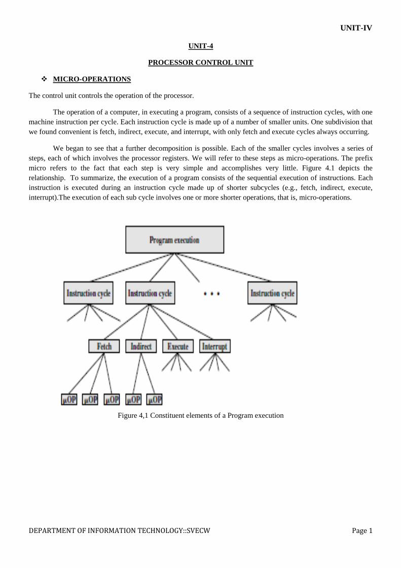
UNIT-IV
DEPARTMENT OF INFORMATION TECHNOLOGY::SVECW Page 1
UNIT-4
PROCESSOR CONTROL UNIT
MICRO-OPERATIONS
The control unit controls the operation of the processor.
The operation of a computer, in executing a program, consists of a sequence of instruction cycles, with one
machine instruction per cycle. Each instruction cycle is made up of a number of smaller units. One subdivision that
we found convenient is fetch, indirect, execute, and interrupt, with only fetch and execute cycles always occurring.
We began to see that a further decomposition is possible. Each of the smaller cycles involves a series of
steps, each of which involves the processor registers. We will refer to these steps as micro-operations. The prefix
micro refers to the fact that each step is very simple and accomplishes very little. Figure 4.1 depicts the
relationship. To summarize, the execution of a program consists of the sequential execution of instructions. Each
instruction is executed during an instruction cycle made up of shorter subcycles (e.g., fetch, indirect, execute,
interrupt).The execution of each sub cycle involves one or more shorter operations, that is, micro-operations.
Figure 4,1 Constituent elements of a Program execution

UNIT-IV
DEPARTMENT OF INFORMATION TECHNOLOGY::SVECW Page 2
The Fetch Cycle
We begin by looking at the fetch cycle, which occurs at the beginning of each instruction cycle and causes
an instruction to be fetched from memory. Four registers are involved:
• Memory address register (MAR): Is connected to the address lines of the system bus. It specifies the
address in memory for a read or write operation.
• Memory buffer register (MBR): Is connected to the data lines of the system bus. It contains the value to
be stored in memory or the last value read from memory.
• Program counter (PC): Holds the address of the next instruction to be fetched.
• Instruction register (IR): Holds the last instruction fetched.
Let us look at the sequence of events for the fetch cycle from the point of view of its effect on the processor
registers. An example appears in Figure 4.2.
4.2 Sequence of events, Fetch cycle
At the beginning of the fetch cycle, the address of the next instruction to be executed is in the program
counter (PC); in this case, the address is 1100100.
The first step is to move that address to the memory address register (MAR) because this is the only register
connected to the address lines of the system bus.
The second step is to bring in the instruction. The desired address (in the MAR) is placed on the address bus,
the control unit issues a READ command on the control bus, and the result appears on the data bus and is
copied into the memory buffer register (MBR). We also need to increment the PC by the instruction length to
get ready for the next instruction. Because these two actions (read word from memory, increment PC) do not
interfere with each other, we can do them simultaneously to save time.
The third step is to move the contents of the MBR to the instruction register (IR). This frees up the MBR for
use during a possible indirect cycle.
Thus, the simple fetch cycle actually consists of three steps and four micro-operations. Symbolically, we can
write this sequence of events as follows:
t1: MAR ← (PC)
t2: MBR ← Memory
PC ← (PC) + I
t3: IR ← (MBR)
where I is the instruction length. Each micro-operation can be performed within the time of a single time unit.The
notation (t1, t2, t3)represents successive time units.In words,we have

UNIT-IV
DEPARTMENT OF INFORMATION TECHNOLOGY::SVECW Page 3
• First time unit: Move contents of PC to MAR.
• Second time unit: Move contents of memory location specified by MAR to MBR. Increment by I the contents of the PC.
• Third time unit: Move contents of MBR to IR.
Note that the second and third micro-operations both take place during the second time unit. The third micro-
operation could have been grouped with the fourth without affecting the fetch operation:
t1: MAR ← (PC)
t2: MBR ← Memory
t3: PC ← (PC) + I
IR ← (MBR)
The groupings of micro-operations must follow three simple rules:
1 The proper sequence of events must be followed. Thus (MAR ; (PC)) must precede (MBR ; Memory)
because the memory read operation makes use of the address in the MAR.
2 Conflicts must be avoided. One should not attempt to read to and write from the same register in one time
unit, because the results would be unpredictable. For example, the micro-operations (MBR ; Memory) and (IR ;
MBR) should not occur during the same time unit.
3 A final point worth noting is that one of the micro-operations involves an addition. To avoid duplication of
circuitry, this addition could be performed by the ALU.
The Indirect Cycle
Once an instruction is fetched, the next step is to fetch source operands. If the instruction specifies an
indirect address, then an indirect cycle must precede the execute cycle and includes the following micro-operations:
t1: MAR ← (IR(Address))
t2: MBR ← Memory
t3: IR(Address) ← (MBR(Address))
The address field of the instruction is transferred to the MAR.This is then used to fetch the address of the operand.
Finally, the address field of the IR is updated from the MBR, so that it now contains a direct rather than an indirect
address. The IR is now in the same state as if indirect addressing had not been used, and it is ready for the execute
cycle.
The Interrupt Cycle
At the completion of the execute cycle, a test is made to determine whether any enabled interrupts have
occurred. If so, the interrupt cycle occurs. The nature of this cycle varies greatly from one machine to another. We
present a very simple sequence of events,
t1: MBR ← (PC)
t2: MAR ← Save_Address
PC ← Routine_Address
t3: Memory ← (MBR)
In the first step, the contents of the PC are transferred to the MBR, so that they can be saved for return from the
interrupt. Then the MAR is loaded with the address at which the contents of the PC are to be saved, and the PC is
loaded with the address of the start of the interrupt-processing routine. These two actions may each be a single
micro-operation. to the MAR and PC, respectively. The final step is to store the MBR, which contains the old value
of the PC, into memory. The processor is now ready to begin the next instruction cycle.

UNIT-IV
DEPARTMENT OF INFORMATION TECHNOLOGY::SVECW Page 4
The Execute Cycle
The fetch, indirect, and interrupt cycles are simple and predictable. Each involves a small, fixed sequence of micro-
operations and, in each case the same micro-operations are repeated each time around.
This is not true of the execute cycle. Because of the variety opcodes, there are a number of different
sequences of micro-operations that can occur.
Let us consider several hypothetical examples.
First, consider an add instruction: ADD R1, X
which adds the contents of the location X to register R1. The following sequence of micro-operations might occur:
t1: MAR ← (IR(address))
t2: MBR ← Memory
t3: R1 ← (R1) + (MBR)
We begin with the IR containing the ADD instruction. In the first step, the address portion of the IR is loaded
into the MAR. Then the referenced memory location is read. Finally, the contents of R1 and MBR are added by the
ALU.
Let us look at two more complex examples.
A common instruction is increment and skip if zero:
ISZ X
The content of location X is incremented by 1. If the result is 0, the next instruction is skipped. A possible sequence
of micro-operations is
t1: MAR ← (IR(address))
t2: MBR ← Memory
t3: MBR ← (MBR) + 1
t4: Memory ← (MBR)
If ((MBR) = 0) then (PC ← (PC) + I)
The new feature introduced here is the conditional action.The PC is incremented if (MBR) = 0. This test and action
can be implemented as one micro-operation.
Finally,consider a subroutine call instruction.As an example,consider a branchand-save-address instruction:
BSA X
The address of the instruction that follows the BSA instruction is saved in location X, and execution
continues at location X + I. The saved address will later be used for return.The following micro-operations suffice:
t1: MAR ← (IR(address))
MBR ← (PC)
t2: PC ← (IR(address))
Memory ← (MBR)
t3: PC ← (PC) + I
The address in the PC at the start of the instruction is the address of the next instruction in sequence. This is
saved at the address designated in the IR. The latter address is also incremented to provide the address of the
instruction for the next instruction cycle.

UNIT-IV
DEPARTMENT OF INFORMATION TECHNOLOGY::SVECW Page 5
The Instruction Cycle
We have seen that each phase of the instruction cycle can be decomposed into a sequence of elementary
micro-operations. There is one sequence each for the fetch, indirect, and interrupt cycles, and, for the execute cycle,
there is one sequence of micro-operations for each opcode.
We assume a new 2-bit register called the instruction cycle code (ICC). The ICC designates the state of the
processor in terms of which portion of the cycle it is in:
00: Fetch
01: Indirect
10: Execute
11: Interrupt
At the end of each of the four cycles, the ICC is set appropriately. The indirect cycle is always followed by
the execute cycle. The interrupt cycle is always followed by the fetch cycle. For both the fetch and execute cycles,
the next cycle depends on the state of the system.
Thus, the flowchart of Figure 4.3 defines the complete sequence of micro-operations, depending only on
the instruction sequence and the interrupt pattern.
Figure 4.3 Flowchart for Instruction Cycle
CONTROL OF THE PROCESSOR
By reducing the operation of the processor to its most fundamental level, we are able to define exactly what it is
that the control unit must cause to happen. Thus, we can define the functional requirements for the control unit:
those functions that the control unit must perform
With the information at hand, the following three-step process leads to a characterization of the control unit:
1 Define the basic elements of the processor.
2 Describe the micro-operations that the processor performs.
3 Determine the functions that the control unit must perform to cause the micro-operations to be performed.
First, the basic functional elements of the processor are the following:
1. ALU 2. Registers 3. Internal data paths 4. External data paths 5.Control Unit

UNIT-IV
DEPARTMENT OF INFORMATION TECHNOLOGY::SVECW Page 6
The ALU is the functional essence of the computer. Registers are used to store data internal to the processor.
Some registers contain status information needed to manage instruction sequencing (e.g., a program status word).
Others contain data that go to or come from the ALU, memory, and I/O modules. Internal data paths are used to
move data between registers and between register and ALU. External data paths link registers to memory and I/O
modules, often by means of a system bus. The control unit causes operations to happen within the processor.
The execution of a program consists of operations involving these processor elements. All micro-operations
fall into one of the following categories:
• Transfer data from one register to another.
• Transfer data from a register to an external interface (e.g., system bus).
• Transfer data from an external interface to a register.
• Perform an arithmetic or logic operation, using registers for input and output.
The control unit performs two basic tasks:
• Sequencing: The control unit causes the processor to step through a series of micro-operations in the
proper sequence, based on the program being executed.
• Execution: The control unit causes each micro-operation to be performed.
The key to how the control unit operates is the use of control signals.
Control Signals
For the control unit to perform its function, it must have inputs that allow it to determine the state of the system and
outputs that allow it to control the behaviour of the system. These are the external specifications of the control unit.
Internally, the control unit must have the logic required to perform its sequencing and execution functions.
Figure 4.4 Block Diagram of Control Unit
Figure 4.4 is a general model of the control unit, showing all of its inputs and outputs. The inputs are
• Clock: This is how the control unit “keeps time.” The control unit causes one micro-operation (or a set of
simultaneous micro-operations) to be performed for each clock pulse. This is sometimes referred to as the
processor cycle time, or the clock cycle time.
• Instruction register: The opcode and addressing mode of the current instruction are used to determine
which micro-operations to perform during the execute cycle.
• Flags: These are needed by the control unit to determine the status of the processor and the outcome of
previous ALU operations. For example, for the increment-and-skip-if-zero (ISZ) instruction, the control unit will
increment the PC if the zero flag is set.
• Control signals from control bus: The control bus portion of the system bus provides signals to the
control unit.

UNIT-IV
DEPARTMENT OF INFORMATION TECHNOLOGY::SVECW Page 7
The outputs are as follows:
• Control signals within the processor: These are two types: those that cause data to be moved from one
register to another, and those that activate specific ALU functions.
• Control signals to control bus: These are also of two types: control signals to memory, and control
signals to the I/O modules.
Three types of control signals are used: those that activate an ALU function, those that activate a data path,
and those that are signals on the external system bus or other external interface.
Let us consider again the fetch cycle to see how the control unit maintains control. The control unit keeps
track of where it is in the instruction cycle. At a given point,it knows that the fetch cycle is to be performed
next.The first step is to transfer the contents of the PC to the MAR. The control unit does this by activating the
control signal that opens the gates between the bits of the PC and the bits of the MAR. The next step is to read a
word from memory into the MBR and increment the PC. The control unit does this by sending the following
control signals simultaneously:
• A control signal that opens gates, allowing the contents of the MAR onto the address bus
• A memory read control signal on the control bus
• A control signal that opens the gates, allowing the contents of the data bus to be stored in the MBR
• Control signals to logic that add 1 to the contents of the PC and store the result back to the PC
Following this, the control unit sends a control signal that opens gates between the MBR and the IR.
This completes the fetch cycle except for one thing: The control unit must decide whether to perform an
indirect cycle or an execute cycle next. To decide this, it examines the IR to see if an indirect memory reference is
made.
The indirect and interrupt cycles work similarly. For the execute cycle, the control unit begins by examining
the opcode and, on the basis of that, decides which sequence of micro-operations to perform for the execute cycle.
A Control Signals Example
To illustrate the functioning of the control unit, let us examine Figure 4.5.This is a simple processor with a
single accumulator (AC). The data paths between elements are indicated. The control paths for signals emanating
from the control unit are not shown, but the terminations of control signals are labeled Ci and indicated by a circle.
4.5 Data paths and control signals
The control unit receives inputs from the clock, the instruction register, and flags. With each clock cycle,
the control unit reads all of its inputs and emits a set of control signals. Control signals go to three separate
destinations:

UNIT-IV
DEPARTMENT OF INFORMATION TECHNOLOGY::SVECW Page 8
• Data paths: The control unit controls the internal flow of data. For example, on instruction fetch, the
contents of the memory buffer register are transferred to the instruction register. For each path to be controlled,
there is a switch (indicated by a circle in the figure). A control signal from the control unit temporarily opens the
gate to let data pass.
• ALU: The control unit controls the operation of the ALU by a set of control signals. These signals activate
various logic circuits and gates within the ALU.
• System bus: The control unit sends control signals out onto the control lines of the system bus (e.g.,
memory READ).
Table 4.1 indicates the control signals that are needed for some of the micro-operation sequences :
Table 4.1 Micro-Operations and Control Signals
8085 ARCHITECTURE The Intel 8085 organization is shown in Figure 4.6. Several key components that may not be self-
explanatory are:
• Incrementer/decrementer address latch: Logic that can add 1 to or subtract 1 from the contents of the
stack pointer or program counter. This saves time by avoiding the use of the ALU for this purpose.
• Interrupt control: This module handles multiple levels of interrupt signals.
• Serial I/O control: This module interfaces to devices that communicate 1 bit at a time.

UNIT-IV
DEPARTMENT OF INFORMATION TECHNOLOGY::SVECW Page 9
Figure 4.6 Intel 8085 CPU Block Diagram
Table 4.2 describes the external signals into and out of the 8085. These are linked to the external system bus. These
signals are the interface between the 8085 processor and the rest of the system.

UNIT-IV
DEPARTMENT OF INFORMATION TECHNOLOGY::SVECW Page 10
Table 4.2 Intel 8085 External Signals

UNIT-IV
DEPARTMENT OF INFORMATION TECHNOLOGY::SVECW Page 11
The control unit is identified as having two components labeled (1) instruction decoder and machine cycle
encoding and (2) timing and control.
The essence of the control unit is the timing and control module.This module includes a clock and accepts as
inputs the current instruction and some external control signals. Its output consists of control signals to the other
components of the processor plus control signals to the external system bus.
The timing of processor operations is synchronized by the clock and controlled by the control unit with
control signals. Each instruction cycle is divided into from one to five machine cycles; each machine cycle is in
turn divided into from three to five states. Each state lasts one clock cycle. During a state, the processor performs
one or a set of simultaneous micro-operations as determined by the control signals.
Figure 4.7 gives an example of 8085 timing, showing the value of external control signals. The diagram
shows the instruction cycle for an OUT instruction. Three machine cycles (M1,M2,M3) are needed.
During the first, the OUT instruction is fetched.
The second machine cycle fetches the second half of the instruction, which contains the number of the I/O
device selected for output.
During the third cycle, the contents of the AC are written out to the selected device over the data bus.
The Address Latch Enabled (ALE) pulse signals the start of each machine cycle from the control unit.The
ALE pulse alerts external circuits.During timing state T1 of machine cycle M1, the control unit sets the IO/M
signal to indicate that this is a memory operation.Also,the control unit causes the contents of the PC to be placed on
the address bus (A15 through A8) and the address/data bus (AD7 through AD0). With the falling edge of the ALE
pulse, the other modules on the bus store the address.
During timing state T2, the addressed memory module places the contents of the addressed memory location
on the address/data bus.
The control unit sets the Read Control (RD) signal to indicate a read, but it waits until T3 to copy the data
from the bus. This gives the memory module time to put the data on the bus and for the signal levels to stabilize.
The final state, T4, is a bus idle state during which the processor decodes the instruction. The remaining machine
cycles proceed in a similar fashion
Figure 4.7 Timing Diagram for Intel 8085 OUT Instruction
HARDWIRED IMPLEMENTATION ` A wide variety of techniques have been used for control unit implementation. Most of these fall into one of
two categories:
• Hardwired implementation
• Microprogrammed implementation
In a hardwired implementation, the control unit is essentially a state machine circuit. Its input logic signals are
transformed into a set of output logic signals, which are the control signals.

UNIT-IV
DEPARTMENT OF INFORMATION TECHNOLOGY::SVECW Page 12
Control Unit Inputs
In Figure 4.4 the key inputs of the control unit are the instruction register, the clock, flags, and control bus
signals. In the case of the flags and control bus signals, each individual bit typically has some meaning (e.g., over-
flow). The other two inputs, however, are not directly useful to the control unit.
First consider the instruction register. The control unit makes use of the opcode and will perform different
actions (issue a different combination of control signals) for different instructions. To simplify the control unit
logic, there should be a unique logic input for each opcode. This function can be performed by a decoder
The clock portion of the control unit issues a repetitive sequence of pulses. This is useful for measuring the
duration of micro-operations. The control unit emits different control signals at different time units within a single
instruction cycle. So the input to the control unit,with a different control signal being used for T1, T2, and so forth.
At the end of an instruction cycle, the control unit must feed back to the counter to reinitialize it at T1.
Figure 4.8 Control Unit with Decoded Inputs
With these two refinements, the control unit can be depicted as in Figure 4.8.
Control Unit Logic
To define the hardwired implementation of a control unit, all that remains is to discuss the internal logic of the
control unit that produces output control signals as a function of its input signals. Essentially, what must be done is,
for each control signal, to derive a Boolean expression of that signal as a function of the inputs.
Let us consider again our simple example illustrated in Figure 4.5. We saw in Table 4.1 the micro-operation
sequences and control signals needed to control three of the four phases of the instruction cycle. Let us consider a
single control signal, C5. This signal causes data to be read from the external data bus into the MBR. We can see
that it is used twice in Table 4.1. Let us define two new control signals, P and Q, that have the following
interpretation:
PQ = 00 Fetch Cycle
PQ = 01 Indirect Cycle
PQ = 10 Execute Cycle
PQ = 11 Interrupt Cycle
Then the following Boolean expression defines
That is, the control signal C5 will be asserted during the second time unit of both the fetch and indirect cycles.
This expression is not complete. C5 is also needed during the execute cycle. For our simple example, let us
assume that there are only three instructions that read from memory: LDA, ADD, and AND. Now we can define C5
as
This same process could be repeated for every control signal generated by the processor. The result would be a set
of Boolean equations that define the behavior of the control unit and hence of the processor.

UNIT-V
DEPARTMENT OF INFORMATION TECHNOLOGY::SVECW Page 1
UNIT-5
MICROPROGRAMMED CONTROL UNIT The term microprogram was first coined by M. V. Wilkes in the early 1950s. Wilkes proposed an approach
to control unit design that was organized and systematic that avoided the complexities of a hardwired
implementation. An alternative for Hardwired Control Unit, which has been used in many CISC processors, is to
implement a microprogrammed control unit.
A language is used to deign microprogrammed control unit known as a microprogramming language. Each
line describes a set of micro-operations occurring at one time and is known as a microinstruction. A sequence of
instructions is known as a microprogram,or firmware.
For each micro-operation, control unit has to do is generate a set of control signals. Thus, for any micro-
operation, control line emanating from the control unit is either on or off. This condition can, be represented by a
binary digit for each control line. So we could construct a control word in which each bit represents one control
line. Now add an address field to each control word, indicating the location of the next control word to be executed
if a certain condition is true.
The result is known as a horizontal microinstruction, which is shown in Figure 5.1a. The format of the
microinstruction or control word is as follows. There is one bit for each internal processor control line and one bit
for each system bus control line. There is a condition field indicating the condition under which there should be a
branch, and there is a field with the address of the microinstruction to be executed next when a branch is taken.
Such a microinstruction is interpreted as follows:
1 To execute this microinstruction, turn on all the control lines indicated by a 1 bit;leave off all control lines
indicated by a 0 bit.The resulting control signals will cause one or more micro-operations to be performed.
2 If the condition indicated by the condition bits is false, execute the next microinstruction in sequence.
3 If the condition indicated by the condition bits is true, the next microinstruction to be executed is indicated
in the address field.
Figure 5.1 Typical MicroInstruction Format
In a vertical microinstruction, a code is used for each action to be performed, and the decoder translates this
code into individual control signals. The advantage of vertical microinstructions is that they are more compact (fewer bits) than horizontal microinstructions.
Figure 5.2 shows how these control words or microinstructions could be arranged in a control memory. The
microinstructions in each routine are to be executed sequentially. Each routine ends with a branch or jump

UNIT-V
DEPARTMENT OF INFORMATION TECHNOLOGY::SVECW Page 2
instruction indicating where to go next. There is a special execute cycle routine whose only purpose is to signify
that one of the machine instruction routines (AND,ADD,and so on) is to be executed next, depending on the current
opcode.
Figure 5.2 Organization of Control Memory
The Figure 5.2 defines the sequence of micro-operations to be performed during each cycle (fetch, indirect,
execute, interrupt), and it specifies the sequencing of these cycles.
Microprogrammed Control Unit
Figure 5.3 Control Unit MicroArchitecture
Figure 5.3 shows the key elements of a microprogrammed control unit implementation. The set of mi-
croinstructions is stored in the control memory. The control address register contains the address of the next
microinstruction to be read. When a microinstruction is read from the control memory, it is transferred to a control
buffer register. The left-hand portion of that register (see Figure 5.1a) connects to the control lines emanating from

UNIT-V
DEPARTMENT OF INFORMATION TECHNOLOGY::SVECW Page 3
the control unit. Thus, reading a microinstruction from the control memory is the same as executing that
microinstruction.The third element shown in the figure is a sequencing unit that loads the control address register
and issues a read command.
Let us examine this structure in greater detail, as depicted in Figure 5.4.The control unit functions as follows:
1 To execute an instruction, the sequencing logic unit issues a READ command to the control memory.
2 The word whose address is specified in the control address register is read into the control buffer register.
3 The content of the control buffer register generates control signals and next-address information for the
sequencing logic unit.
4 The sequencing logic unit loads a new address into the control address register based on the next-address
information from the control buffer register and the ALU flags.
Figure 5.4 Functioning of microprogrammed control unit
At the conclusion of each microinstruction, the sequencing logic unit loads a new address into the control
address register. Depending on the value of the ALU flags and the control buffer register, one of three decisions is
made:
• Get the next instruction: Add 1 to the control address register.
• Jump to a new routine based on a jump microinstruction: Load the address field of the control buffer register into the control address register.
• Jump to a machine instruction routine: Load the control address register based on the opcode in the IR.
Figure 5.4 shows two modules labeled decoder. The upper decoder translates the opcode of the IR into a
control memory address. The lower decoder is not used for horizontal microinstructions but is used for vertical
microinstructions (Figure 5.1b). In a horizontal microinstruction every bit in the control field attaches to a control
line. In a vertical microinstruction, a code is used for each action to be performed, and the decoder translates this
code into individual control signals. The advantage of vertical microinstructions is that they are more compact (fewer bits) than horizontal microinstructions.

UNIT-V
DEPARTMENT OF INFORMATION TECHNOLOGY::SVECW Page 4
Advantages and Disadvantages
The principal advantage of the use of microprogramming to implement a control unit is that it simplifies
the design of the control unit. Thus, it is both cheaper and less error prone to implement. A hardwired control unit
must contain complex logic for sequencing through the many micro-operations of the instruction cycle. On the
other hand, the decoders and sequencing logic unit of a microprogrammed control unit are very simple pieces of
logic.
The principal disadvantage of a microprogrammed unit is that it will be somewhat slower than a hardwired
unit of comparable technology. Despite this, microprogramming is the dominant technique for implementing
control units in pure CISC architectures, due to its ease of implementation. RISC processors, with their simpler
instruction format, typically use hardwired control units.
MICROINSTRUCTION SEQUENCING The two basic tasks performed by a microprogrammed control unit are as follows:
• Microinstruction sequencing: Get the next microinstruction from the control memory.
• Microinstruction execution: Generate the control signals needed to execute the microinstruction.
In designing a control unit, these tasks must be considered together, because both affect the format of the
microinstruction and the timing of the control unit.
Design Considerations
Two concerns are involved in the design of a microinstruction sequencing technique: the size of the
microinstruction and the address-generation time. The first concern is obvious; minimizing the size of the control
memory reduces the cost of that component. The second concern is simply a desire to execute microinstructions as
fast as possible.
In executing a microprogram, the address of the next microinstruction to be executed is in one of these
categories:
• Determined by instruction register
• Next sequential address
• Branch
Sequencing Techniques
Based on the current microinstruction, condition flags, and the contents of the instruction register, a control
memory address must be generated for the next microinstruction. A wide variety of techniques have been used.
These categories are based on the format of the address information in the microinstruction:
• Two address fields
• Single address field
• Variable format
Two Address Field:
The simplest approach is to provide two address fields in each microinstruction. Figure 5.5 suggests how this
information is to be used. A multiplexer is provided that serves as a destination for both address fields plus the
instruction register. Based on an address-selection input, the multiplexer transmits either the opcode or one of the
two addresses to the control address register (CAR). The CAR is subsequently decoded to produce the next
microinstruction address.The address-selection signals are provided by a branch logic module whose input consists
of control unit flags plus bits from the control portion of the microinstruction.
Although the two-address approach is simple, it requires more bits in the microinstruction than other
approaches. With some additional logic, savings can be achieved.

UNIT-V
DEPARTMENT OF INFORMATION TECHNOLOGY::SVECW Page 5
Figure 5.5 Branch Control Logic: Two Address Field
Single Address Field:
Figure 5.6 Branch Control Logic: Single Address Field

UNIT-V
DEPARTMENT OF INFORMATION TECHNOLOGY::SVECW Page 6
A common approach is to have a single address field (Figure 5.6). With this approach, the options for next
address are as follows:
• Address field
• Instruction register code
• Next sequential address
The address-selection signals determine which option is selected. This approach reduces the number of address
fields to one. Note, however, that the address field often will not be used. Thus, there is some inefficiency in the
microinstruction coding scheme.
Variable Format:
Another approach is to provide for two entirely different microinstruction formats (Figure 5.7). One bit
designates which format is being used. In one format, the remaining bits are used to activate control signals. In the
other format, some bits drive the branch logic module, and the remaining bits provide the address.
One disadvantage of this second approach is that one entire cycle is consumed with each branch
microinstruction. With the other approaches, address generation occurs as part of the same cycle as control signal
generation, minimizing control memory accesses.
Figure 5.7 Branch Control Logic: Variable Format
Address Generation
There are various ways in which the next address can be derived or computed.
Table 5.1 lists the various address generation techniques. These can be divided into explicit techniques, in
which the address is explicitly available in the microinstruction, and implicit techniques, which require additional
logic to generate the address.

UNIT-V
DEPARTMENT OF INFORMATION TECHNOLOGY::SVECW Page 7
Table 5.1 MicroInstruction Address Generation Techniques
We have essentially dealt with the explicit techniques. With a two-field approach, two alternative addresses
are available with each microinstruction. Using either a single address field or a variable format, various branch
instructions can be implemented. A conditional branch instruction depends on the following types of information:
• ALU flags
• Part of the opcode or address mode fields of the machine instruction
• Parts of a selected register, such as the sign bit
• Status bits within the control unit
Several implicit techniques are also commonly used. One of these, mapping, is required with virtually all
designs. The opcode portion of a machine instruction must be mapped into a microinstruction address.This occurs
only once per instruction cycle. A common implicit technique is Addition that involves combining or adding two
portions of an address to form the complete address. The final approach is termed residual control. This approach
involves the use of a microinstruction address that has previously been saved in temporary storage within the
control unit. An example of this approach is taken on the LSI-11.
LSI-11 Microinstruction Sequencing
The LSI-11 is a microcomputer version of a PDP-11, which is implemented using a microprogrammed
control unit.
The LSI-11 makes use of a 22-bit microinstruction and a control memory of 2K 22-bit words. The next
microinstruction address is determined in one of five ways:
• Next sequential address: In the absence of other instructions, the control unit’s control address register is
incremented by 1.
• Opcode mapping: At the beginning of each instruction cycle, the next microinstruction address is
determined by the opcode.
• Subroutine facility: Explained presently.
• Interrupt testing: Certain microinstructions specify a test for interrupts. If an interrupt has occurred, this
determines the next microinstruction address.
• Branch: Conditional and unconditional branch microinstructions are used.
MICROINSTRUCTION EXECUTION
The microinstruction cycle is the basic event on a microprogrammed processor. Each cycle is made up of
two parts: fetch and execute. The fetch portion is determined by the generation of a microinstruction address and
the execution of a microinstruction is to generate control signals. Some of these signals control points internal to
the processor. The remaining signals go to the external control bus or other external interface.
A Taxonomy of Microinstructions
Microinstructions can be classified in a variety of ways. Distinctions that are commonly made in the literature
include the following:
• Vertical/horizontal
• Packed/unpacked
• Hard/soft microprogramming
• Direct/indirect encoding

UNIT-V
DEPARTMENT OF INFORMATION TECHNOLOGY::SVECW Page 8
Horizontal/Vertical microinstruction: Each bit of a microinstruction either directly produced a control signal or
directly produced one bit of the next address. These schemes require a more complex sequencing logic module.
Packed/Unpacked Microinstruction: The degree of packing relates to the degree of identification between a
given control task and specific microinstruction bits. As the bits become more packed, a given number of bits
contains more information. Thus, packing connotes encoding. The terms horizontal and vertical relate to the
relative width of microinstructions. The terms hard and soft microprogramming are used to suggest the degree of
closeness to the underlying control signals and hardware layout. Hard microprograms are generally fixed and
committed to read-only memory. Soft microprograms are more changeable and are suggestive of user
microprogramming. The other pair is direct versus indirect encoding.
Microinstruction Encoding
Some degree of encoding is used to reduce control memory width and to simplify the task of microprogramming.
The basic technique for encoding is illustrated in Figure 5.8a. The microinstruction is organized as a set of
fields. Each field contains a code, which, upon decoding, activates one or more control signals. When the
microinstruction is executed, every field is decoded and generates control signals.Thus, with N fields, N
simultaneous actions are specified. Each action results in the activation of one or more control signals
Figure 5.8 MicroInstruction Encoding
The design of an encoded microinstruction format can now be stated in simple terms:
• Organize the format into independent fields. That is, each field depicts a set of actions (pattern of control
signals) such that actions from different fields can occur simultaneously.
• Define each field such that the alternative actions that can be specified by the field are mutually exclusive.
That is, only one of the actions specified for a given field could occur at a time.
Two approaches can be taken to organizing the encoded microinstruction into fields: functional and resource.
The functional encoding method identifies functions within the machine and designates fields by function type.
For example, if various sources can be used for transferring data to the accumulator, one field can be designated for
this purpose, with each code specifying a different source. Resource encoding views the machine as consisting of a
set of independent resources and devotes one field to each (e.g., I/O, memory, ALU).
Another aspect of encoding is whether it is direct or indirect (Figure 5.8b). With indirect encoding, one field
is used to determine the interpretation of another field.