wear mechanisms of uncoated and coated cemented carbide
TRANSCRIPT
LUND UNIVERSITY
PO Box 117221 00 Lund+46 46-222 00 00
Wear mechanisms of uncoated and coated cemented carbide tools in machining lead-free silicon brass
Bushlya, Volodymyr; Johansson, Daniel; Lenrick, Filip; Ståhl, Jan Eric; Schultheiss, Fredrik
Published in:Wear
DOI:10.1016/j.wear.2017.01.039
2017
Document Version:Early version, also known as pre-print
Link to publication
Citation for published version (APA):Bushlya, V., Johansson, D., Lenrick, F., Ståhl, J. E., & Schultheiss, F. (2017). Wear mechanisms of uncoatedand coated cemented carbide tools in machining lead-free silicon brass. Wear, 376-377, 143-151.https://doi.org/10.1016/j.wear.2017.01.039
Total number of authors:5
General rightsUnless other specific re-use rights are stated the following general rights apply:Copyright and moral rights for the publications made accessible in the public portal are retained by the authorsand/or other copyright owners and it is a condition of accessing publications that users recognise and abide by thelegal requirements associated with these rights. • Users may download and print one copy of any publication from the public portal for the purpose of private studyor research. • You may not further distribute the material or use it for any profit-making activity or commercial gain • You may freely distribute the URL identifying the publication in the public portal
Read more about Creative commons licenses: https://creativecommons.org/licenses/Take down policyIf you believe that this document breaches copyright please contact us providing details, and we will removeaccess to the work immediately and investigate your claim.
Wear mechanisms of uncoated and coated cemented carbide tools in machining lead-free silicon brass
Volodymyr Bushlya*, Daniel Johansson, Filip Lenrick, Jan-Eric Ståhl, Fredrik Schultheiss
Division of Production and Materials Engineering, Lund University, S-221 00 Lund, Sweden
Abstract
Free-machining brass containing 2 to 3 % of lead is a preferred industrial material as it shows excellent machinability where low cutting forces, short chips and reduced tool wear are attained. However this addition of lead, a highly toxic and hazardous material, leads to health and environmental issues. Alternative lead-free brasses are known for poor chip control and accelerated tool wear. The current study focuses on wear mechanisms of uncoated and coated cemented carbide tools when high-speed machining lead-free CuZn21Si3P silicon brass. The study shows that severe crater formation on the rake is the dominant tool failure mode. Microscopy observations indicate the diffusion wear mechanism to be driven by diffusion of cobalt binder into the chips and minor cross-diffusion of copper and zinc. Loss of the binder in cemented carbide is accompanied by adhesive pluck-out of WC grains. As a way to hinder the loss of Co, the capacity of a-C:H diamond like carbon and (Ti,V,Zr,Nb,Hf,Ta)N nitride coating to act as diffusion barriers were tested. SEM, EDX and TEM data show that formation of amorphous SiO2 and stoichiometric β-SiAlON stable layers was observed on the nitride coating, thus preventing diffusional tool wear. O-rich and N-rich glassy amorphous layers with ZnS inclusions were found on the DLC coating. Partial delamination of the DLC coating and removal of the glassy phases resulted in localized crater formation associated with diffusional wear.
1. Introduction
Brass is a copper and zinc alloy, frequently used for a wide range of applications including household products, door handles, nuts and screws, plumbing fittings, etc. [1]. Additional alloying elements such as lead, silicon, aluminum, iron, tin, manganese, nickel or arsenic are also commonly found in modern brass varieties [2]. So-called free-machining brasses generally contain roughly 3 wt. % lead as a mean of improving the machinability of the material [3]. The addition of lead improves the machinability by enhancing chip breaking, lowering cutting forces, decreasing tool wear, and permitting better surface roughness and tolerances [4, 5].
Lead is a heavy metal which is toxic even at low levels of exposure [6]. Even so, the International Lead and Zinc Study Group (ILZSG) found that 115,000 tons of lead were used in different alloys in the countries reporting to the organization during 2003. This is estimated to be equivalent to roughly 80% of the world consumption during the same time period [6]. The use of lead in alloys is increasingly discouraged, primarily due to the substantially detrimental effects on the environment.
Inside the European Union copper alloys are currently permitted to contain up to 4 wt. % lead according to the directive on the restriction of use of certain hazardous substances, RoHS, and the directive on end-of-life vehicles, ELV, [7, 8]. As the importance of sustainable production is becoming increasingly recognize, further legislative actions limiting the use of lead are expected in the future as highlighted by Nobel et al. [9], although none has thus far been announced. Worth noticing is that already by 1956 the USSR adopted a standard specifying that the amount of lead in brasses intended for food and medical applications was not allowed to exceed 0.05 wt. % [10].
Lead is soluble in molten brass but precipitates at the grain boundaries during solidification, commonly forming particles 1-10 μm in diameter [11]. As anticipated, the size and distribution of these lead globules have been found to affect the machinability of the material [12]. Trent and Wright [11] found that the addition of lead in brass greatly reduces the cutting forces, shortens the chips and decreases the tool wear. The reason for this is claimed to be lead strongly adhering to the tool contact area, thus acting as an “internal lubricant” [13]. Several alternative alloying elements, as a replacement for lead, have been proposed, one of the more common being silicon. As expressed by Taha et al. [14], the substitution of lead with silicon is believed to result in slightly decreased machinability, which has to be weighed against the improved sustainability.
Majority of the studies on the machinability of silicon alloyed brass are focusing on friction [15], chip formation [9, 16, 17] and surface quality [18] in cutting lead-free brasses. The issues of tool wear and mechanisms governing accelerated tool deterioration while machining lead-free brass are hardly touched [18, 19].

Therefore, the study presented in this article aims at comparing the tool wear and analyzing wear mechanisms acting for uncoated and coated cemented carbide tooling when machining CuZn39Pb3 free-machining brass as compared to the commercially available, CuZn21Si3P lead-free alternative.
2. Materials
The machining tests were conducted for CuZn39Pb3 free-machining brass containing 3.3 wt.% of lead and CuZn21Si3P lead-free brass containing 3 wt.% silicon, as shown in Table 1. Scanning electron microscope (SEM) images showing the typical microstructure for the two investigated materials can be found in Figure 1. Both brasses are dual-phase where CuZn39Pb3 contains roughly 70% α-phase and 30% β-phase, CuZn21Si3P contains roughly 60% α-phase and 40% κ-phase. Ductile α-phase (fcc) introduces machinability issues, both by adhering to the tool materials and by limiting chip breakage and handling [19]. Presence of lead in CuZn39Pb3 alleviates the problems because its low melting temperature (327.5 °C) which introduces a lubricating effect on the tool-chip interface and facilitates separation of individual chip segments into needle chips [9, 16].
Table 1. Chemical composition according to nominal standards (wt. %) [20, 21].
Material Cu Zn Pb Si P
CuZn39Pb3 57.3 Balance 3.3 - -
CuZn21Si3P 76 Balance <0.09 3 0.05
Presence of κ-phase (hcp) [22] in CuZn21Si3P brass, which possesses high hardness of H = 3.3 GPa [18] and thus brittleness, has a similar role as it enables formation of segmented, instead of continuous, chips.
Fig. 1. SEM of microstructure of Pb-brass and Si-brass
Table 2. Properties of free-machining CuZn39Pb3 and lead-free CuZn21Si3P silicon brass [18].
Material property CuZn39Pb3 CuZn21Si3P
Yield strength, Rp [MPa] 201 342
Tensile strength, Rm [MPa] 525 717
Elongation at rupture, εb [-] 0.26 0.22
Hardness, H [GPa] 1.90 2.98
Thermal conductivity, kW [W/mK] 113 35
The higher strength, bulk hardness and lower thermal conductivity of CuZn21Si3P lead-free brass (Table 2) are also expected to contribute to the formation of segmented chips, as shown in [16, 19].
3. Experimental setup

The machining tests comprised of longitudinal turning on a conventional CNC lathe. Both investigated materials were supplied as bars having the diameter of 50 mm. Experiments for the analysis of cutting force were carried out at cutting speed vc = 400 m/min at varying feed (f = 0.05 – 0.3 mm/rev). Large depth-of-cut (ap = 2.5 mm) was selected to minimize the effect of tool nose radius on the obtained data. Tool wear tests were conducted at cutting conditions typical for semi-finishing (vc = 400 m/min, f = 0.20 mm/rev and ap = 0.8 mm). Cutting force tests and initial tool wear experiments involved machining with uncoated cemented carbide tooling. Fine-grained H10F cemented carbide grade having 10% cobalt binder (Fig. 2) was used. DNGA150708F inserts were cut by wire electrical discharge machining (wire-EDM) from bulk cemented carbide sample and finish ground to achieve edge radius of approximately 10±5 μm. The inserts were in turn mounted in a PDJNL3225P15 tool holder providing side rake γf = -6°, back rake γp = -6° and major cutting edge angle κ = 93°.
Fig. 2. SEM of microstructure of H10F cemented carbide grade.
Two coatings where additionally applied on the H10F cemented carbide substrate in order to improve the machinability of CuZn21Si3P silicon brass and wear resistance of tooling during machining. Commercial multi-layered diamond like carbon (DLC) coating which consists of Cr/CrxCy and a-C:H (amorphous hydrogenated carbon) layers (Fig. 3.a) was used, as it possesses high hardness (H ≈ 30 GPa) [23] and low friction in machining brass alloys [19]. Thickness of the DLC coating was 2 μm. TiN nitride coating were also shown to exhibit low friction in brass machining, yet low hardness of TiN coating resulted in poor performance [19]. High hardness (H = 34 GPa) experimental single layer nitride (Ti,V,Zr,Hf,Nb,Ta)N coating was also tested. The coating was deposited by vacuum-arc evaporation of a Ti-V-Zr-Hf-Nb-Ta high entropy alloy target [24]. The thickness of this nitride coating was 4 μm (Fig. 3.b).
Fig. 3. SEM image of (a) a-C:H diamond like carbon and (b) (Ti,V,Zr,Hf,Nb,Ta)N coatings.
Cutting forces were measured with Kistler 9129AA dynamometer. Alicona InfiniteFocus 3D optical microscope was used for 3D analysis of worn tools. LEO/Zeiss 1560 high resolution scanning electron microscope (SEM) was used for the analysis of workpiece materials, new and worn tools. FEI NanoLab 600 dual beam microscope was used for lamella preparation using focused ion beam (FIB) lift-out technique [25]. JEOL 3000F transmission electron microscope (TEM) was used for imaging, selected
area electron diffraction (SAED) and energy dispersive X-ray (EDX) analysis (SDD X-Maxn EDX system, Oxford Instruments).
4. Results and discussion
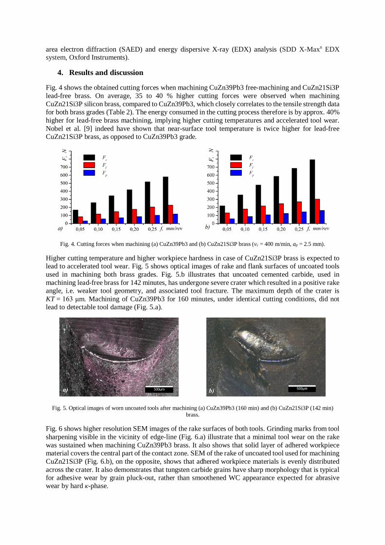
Fig. 4 shows the obtained cutting forces when machining CuZn39Pb3 free-machining and CuZn21Si3P lead-free brass. On average, 35 to 40 % higher cutting forces were observed when machining CuZn21Si3P silicon brass, compared to CuZn39Pb3, which closely correlates to the tensile strength data for both brass grades (Table 2). The energy consumed in the cutting process therefore is by approx. 40% higher for lead-free brass machining, implying higher cutting temperatures and accelerated tool wear. Nobel et al. [9] indeed have shown that near-surface tool temperature is twice higher for lead-free CuZn21Si3P brass, as opposed to CuZn39Pb3 grade.
Fig. 4. Cutting forces when machining (a) CuZn39Pb3 and (b) CuZn21Si3P brass (vc = 400 m/min, ap = 2.5 mm).
Higher cutting temperature and higher workpiece hardness in case of CuZn21Si3P brass is expected to lead to accelerated tool wear. Fig. 5 shows optical images of rake and flank surfaces of uncoated tools used in machining both brass grades. Fig. 5.b illustrates that uncoated cemented carbide, used in machining lead-free brass for 142 minutes, has undergone severe crater which resulted in a positive rake angle, i.e. weaker tool geometry, and associated tool fracture. The maximum depth of the crater is KT = 163 μm. Machining of CuZn39Pb3 for 160 minutes, under identical cutting conditions, did not lead to detectable tool damage (Fig. 5.a).
Fig. 5. Optical images of worn uncoated tools after machining (a) CuZn39Pb3 (160 min) and (b) CuZn21Si3P (142 min) brass.
Fig. 6 shows higher resolution SEM images of the rake surfaces of both tools. Grinding marks from tool sharpening visible in the vicinity of edge-line (Fig. 6.a) illustrate that a minimal tool wear on the rake was sustained when machining CuZn39Pb3 brass. It also shows that solid layer of adhered workpiece material covers the central part of the contact zone. SEM of the rake of uncoated tool used for machining CuZn21Si3P (Fig. 6.b), on the opposite, shows that adhered workpiece materials is evenly distributed across the crater. It also demonstrates that tungsten carbide grains have sharp morphology that is typical for adhesive wear by grain pluck-out, rather than smoothened WC appearance expected for abrasive wear by hard κ-phase.
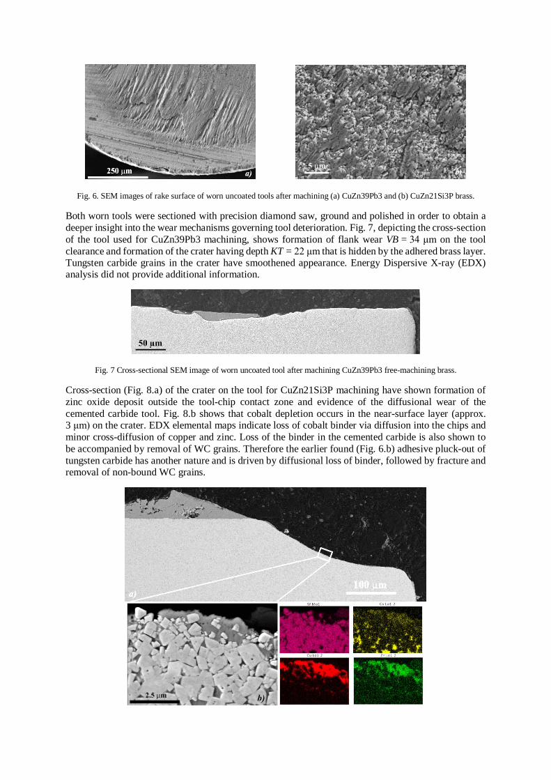
Fig. 6. SEM images of rake surface of worn uncoated tools after machining (a) CuZn39Pb3 and (b) CuZn21Si3P brass.
Both worn tools were sectioned with precision diamond saw, ground and polished in order to obtain a deeper insight into the wear mechanisms governing tool deterioration. Fig. 7, depicting the cross-section of the tool used for CuZn39Pb3 machining, shows formation of flank wear VB = 34 μm on the tool clearance and formation of the crater having depth KT = 22 μm that is hidden by the adhered brass layer. Tungsten carbide grains in the crater have smoothened appearance. Energy Dispersive X-ray (EDX) analysis did not provide additional information.
Fig. 7 Cross-sectional SEM image of worn uncoated tool after machining CuZn39Pb3 free-machining brass.
Cross-section (Fig. 8.a) of the crater on the tool for CuZn21Si3P machining have shown formation of zinc oxide deposit outside the tool-chip contact zone and evidence of the diffusional wear of the cemented carbide tool. Fig. 8.b shows that cobalt depletion occurs in the near-surface layer (approx. 3 μm) on the crater. EDX elemental maps indicate loss of cobalt binder via diffusion into the chips and minor cross-diffusion of copper and zinc. Loss of the binder in the cemented carbide is also shown to be accompanied by removal of WC grains. Therefore the earlier found (Fig. 6.b) adhesive pluck-out of tungsten carbide has another nature and is driven by diffusional loss of binder, followed by fracture and removal of non-bound WC grains.

Fig. 8 Cross-section on Si-brass (a). SEM/EDX of Co diffusion (VB)
Both, a-C:H and (Ti,V,Zr,Nb,Hf,Ta)N, coatings possess higher hardness than the cemented carbide substrate and can act as diffusional barriers, thus blocking or retarding the abrasive and diffusional wear mechanisms found for uncoated tools. The wear tests were carried out only for machining CuZn21Si3P silicon brass as it has shown the worst machinability. The tests were carried out at identical machining conditions as for uncoated ones, and the tool wear was analyzed after 145 minutes of cutting.
Fig. 9.a shows that the major part of the DLC coating has been delaminated during machining and initial signs of crater development are present. The maximum depth of the crater is 53 μm. It also shows that up to 30% of the tool-chip contact area is covered by a layer or deposit. More detailed inspection of the area indicates that this layer in the central part of the tool is deposited directly on the non-delaminated sector of DLC coating, while the layers in other regions are deposited on the already formed crater surfaces. Similar deposit of much smaller dimensions (50 μm by 20 μm) was also found in the crater of uncoated tool. The 50 μm to 100 μm wide band along the edge-line also does not have DLC coating, yet no crater formation is observed, leaving the intact plateau of the original cemented carbide substrate. Fig. 9.b shows that an identical band devoid of the coating exists in the case of (Ti,V,Zr,Nb,Hf,Ta)N coating. The rest of the tool-chip contact zone is completely covered by a layer or deposit. It also shows that the tool did not suffer from crater wear, and even the grinding marks are visible in the plateau region. This indicates that the formed deposit on the rake surface acts as a tool protection layer (TPL) by blocking the diffusion of Co binder and abrasive wear.
Fig. 9. SEM overview of the worn (a) DLC and (b) (Ti,V,Zr,Nb,Hf,Ta)N coated tools (145 min).
Both coated tools were sectioned with the diamond saw and polished similarly to the uncoated cemented carbide tools. The cross-section on the DLC tool was carried out through the tool protection layer located in the crater (Fig. 10.a). More than half of the crater, further from the edge-line, is covered by TPL, which has thickness of 3 μm to 10 μm. Tool protection layer extends even beyond the tool-chip contact zone. As with the uncoated insert, the primary wear mechanism is Co diffusion which is shown by the reduced levels of Co close to the surface seen in Fig. 10.c. The figure however shows that Co was not completely removed or replaced by Cu and Zn, as is the case of uncoated tool, which gives an evidence of protective action of TPL. Flank wear VB = 56 μm on the tool clearance is also present, apart from the crater.

Fig. 10 (a) SEM overview of the crater in the DLC tool. (b) SEM image of the region where a FIB lamella was extracted. (c) SEM image and EDX Co Kα map of a near-surface region in the crater.
To gain a deeper understanding of the composition of this tool protection layer and mechanisms of its formation a cross-sectional FIB lamella for TEM analysis was extracted from the crater of the worn DCL insert. The lamella was extracted at right angle to the surface of cemented carbide in the region shown in Fig. 10.b.
Fig. 11. (a) STEM HAADF image of the lamella extracted from the crater in the DLC insert with regions for SAED and
DFTEM marked. (b) EDX maps (Si Kα, Al Kα, O Kα, N Kα, Zn Kα, S Kα) with regions for SAED marked.
Five major layers are identifiable in the STEM HAADF image of the TPL (Fig.11.a). Among them, two thick (200-500 nm) layers have higher oxygen content (seen as dark grey in Fig.11.a) and three thinner (50-150 nm) layer of laminar structure (seen as middle grey in grey in Fig.11.a). Each of the thinner layers consists of alternating lamellae of ZnS and nitrogen enriched ceramic which can be as thin as 100 nm (Fig. 12.d). ZnS was identified to be crystalline with cubic zinkblende structure (Sphalerite) while both nitrogen rich and oxygen rich layers to be amorphous, as seen in Fig. 12. Both types of amorphous ceramic layers are from Si-Al-O-N system.
Table 3 presents chemical composition data for the identified layers in the TPL. Oxygen rich phase maintains the ratio between Si and O rather close to silicon oxide SiO2, however a slight excess of Si and minor concentration of aluminum and nitrogen are also present. The nitrogen rich phase is compositionally close to silicon nitride and β-SiAlON, yet excess of oxygen and significant lack of nitrogen does not allow classifying it as either of the mentioned compounds.
Table 3. Chemical composition (at.%) of TPL layer in different locations of uncoated and coated tools.
Tool Phase Si Al O N Uncoated O rich phase 21.2 ± 0.48 3.9 ± 0.06 32.8 ± 1.17 15.1 ± 0.84
DLC O rich phase 33.7 ± 0.87 1.25 ± 0.32 61.5 ± 1.37 3.4 ± 0.81 N rich phase 47.9 ± 1.02 5.2 ± 0.27 4.9 ± 0.55 41.9 ± 1.31
(Ti,V,Zr,Hf,Nb,Ta)N SiO2 25.2 ± 0.18 1.3 ± 0.13 49.6 ± 0.21 -
N rich phase 28.1 ± 1.60 4.2 ± 0.68 5.8 ± 0.67 35.9 ± 2.19 O rich phase 40.5 ± 0.73 4.6 ± 0.34 45.4 ± 0.92 11.0 ± 1.17
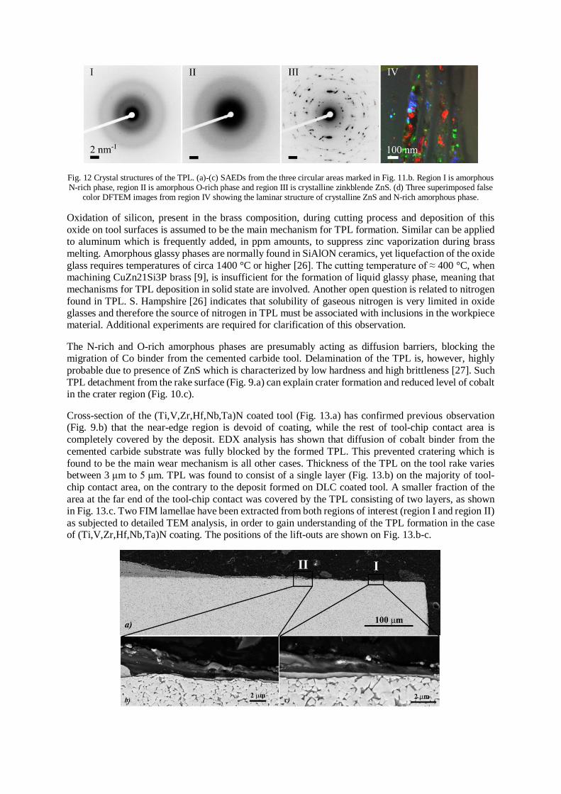
Fig. 12 Crystal structures of the TPL. (a)-(c) SAEDs from the three circular areas marked in Fig. 11.b. Region I is amorphous N-rich phase, region II is amorphous O-rich phase and region III is crystalline zinkblende ZnS. (d) Three superimposed false
color DFTEM images from region IV showing the laminar structure of crystalline ZnS and N-rich amorphous phase.
Oxidation of silicon, present in the brass composition, during cutting process and deposition of this oxide on tool surfaces is assumed to be the main mechanism for TPL formation. Similar can be applied to aluminum which is frequently added, in ppm amounts, to suppress zinc vaporization during brass melting. Amorphous glassy phases are normally found in SiAlON ceramics, yet liquefaction of the oxide glass requires temperatures of circa 1400 °C or higher [26]. The cutting temperature of ≈ 400 °C, when machining CuZn21Si3P brass [9], is insufficient for the formation of liquid glassy phase, meaning that mechanisms for TPL deposition in solid state are involved. Another open question is related to nitrogen found in TPL. S. Hampshire [26] indicates that solubility of gaseous nitrogen is very limited in oxide glasses and therefore the source of nitrogen in TPL must be associated with inclusions in the workpiece material. Additional experiments are required for clarification of this observation.
The N-rich and O-rich amorphous phases are presumably acting as diffusion barriers, blocking the migration of Co binder from the cemented carbide tool. Delamination of the TPL is, however, highly probable due to presence of ZnS which is characterized by low hardness and high brittleness [27]. Such TPL detachment from the rake surface (Fig. 9.a) can explain crater formation and reduced level of cobalt in the crater region (Fig. 10.c).
Cross-section of the (Ti,V,Zr,Hf,Nb,Ta)N coated tool (Fig. 13.a) has confirmed previous observation (Fig. 9.b) that the near-edge region is devoid of coating, while the rest of tool-chip contact area is completely covered by the deposit. EDX analysis has shown that diffusion of cobalt binder from the cemented carbide substrate was fully blocked by the formed TPL. This prevented cratering which is found to be the main wear mechanism is all other cases. Thickness of the TPL on the tool rake varies between 3 μm to 5 μm. TPL was found to consist of a single layer (Fig. 13.b) on the majority of tool-chip contact area, on the contrary to the deposit formed on DLC coated tool. A smaller fraction of the area at the far end of the tool-chip contact was covered by the TPL consisting of two layers, as shown in Fig. 13.c. Two FIM lamellae have been extracted from both regions of interest (region I and region II) as subjected to detailed TEM analysis, in order to gain understanding of the TPL formation in the case of (Ti,V,Zr,Hf,Nb,Ta)N coating. The positions of the lift-outs are shown on Fig. 13.b-c.
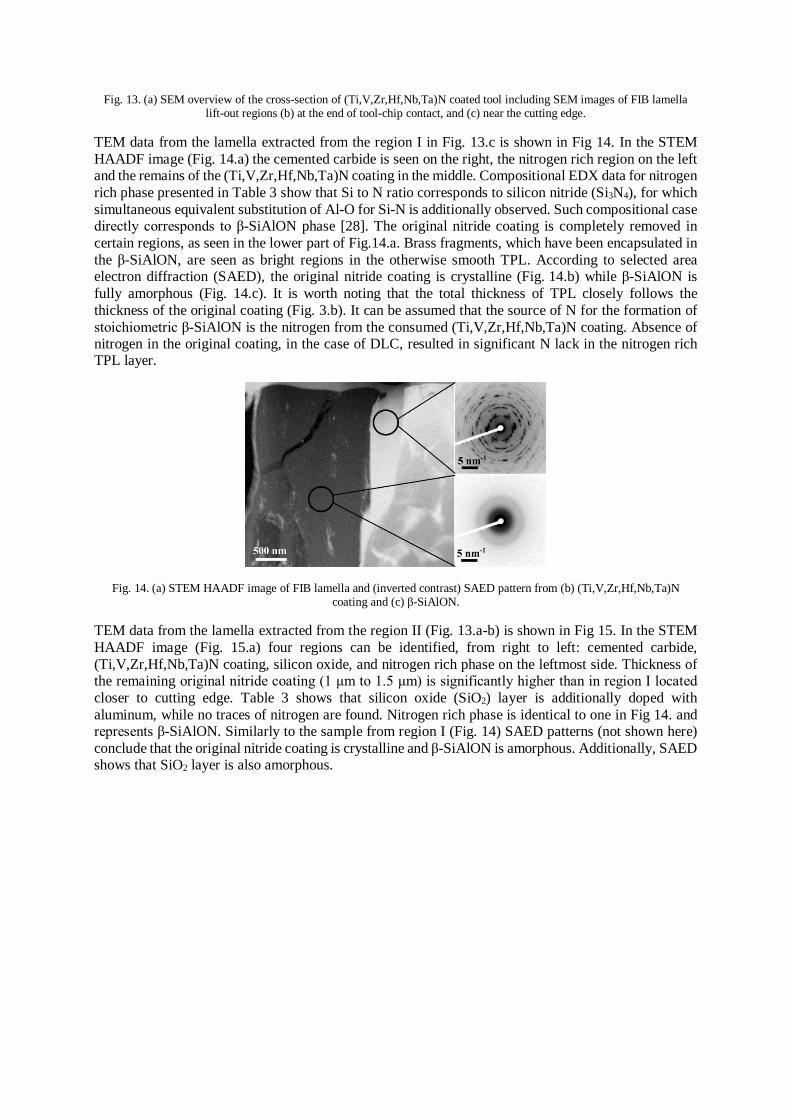
Fig. 13. (a) SEM overview of the cross-section of (Ti,V,Zr,Hf,Nb,Ta)N coated tool including SEM images of FIB lamella lift-out regions (b) at the end of tool-chip contact, and (c) near the cutting edge.
TEM data from the lamella extracted from the region I in Fig. 13.c is shown in Fig 14. In the STEM HAADF image (Fig. 14.a) the cemented carbide is seen on the right, the nitrogen rich region on the left and the remains of the (Ti,V,Zr,Hf,Nb,Ta)N coating in the middle. Compositional EDX data for nitrogen rich phase presented in Table 3 show that Si to N ratio corresponds to silicon nitride (Si3N4), for which simultaneous equivalent substitution of Al-O for Si-N is additionally observed. Such compositional case directly corresponds to β-SiAlON phase [28]. The original nitride coating is completely removed in certain regions, as seen in the lower part of Fig.14.a. Brass fragments, which have been encapsulated in the β-SiAlON, are seen as bright regions in the otherwise smooth TPL. According to selected area electron diffraction (SAED), the original nitride coating is crystalline (Fig. 14.b) while β-SiAlON is fully amorphous (Fig. 14.c). It is worth noting that the total thickness of TPL closely follows the thickness of the original coating (Fig. 3.b). It can be assumed that the source of N for the formation of stoichiometric β-SiAlON is the nitrogen from the consumed (Ti,V,Zr,Hf,Nb,Ta)N coating. Absence of nitrogen in the original coating, in the case of DLC, resulted in significant N lack in the nitrogen rich TPL layer.
Fig. 14. (a) STEM HAADF image of FIB lamella and (inverted contrast) SAED pattern from (b) (Ti,V,Zr,Hf,Nb,Ta)N coating and (c) β-SiAlON.
TEM data from the lamella extracted from the region II (Fig. 13.a-b) is shown in Fig 15. In the STEM HAADF image (Fig. 15.a) four regions can be identified, from right to left: cemented carbide, (Ti,V,Zr,Hf,Nb,Ta)N coating, silicon oxide, and nitrogen rich phase on the leftmost side. Thickness of the remaining original nitride coating (1 μm to 1.5 μm) is significantly higher than in region I located closer to cutting edge. Table 3 shows that silicon oxide (SiO2) layer is additionally doped with aluminum, while no traces of nitrogen are found. Nitrogen rich phase is identical to one in Fig 14. and represents β-SiAlON. Similarly to the sample from region I (Fig. 14) SAED patterns (not shown here) conclude that the original nitride coating is crystalline and β-SiAlON is amorphous. Additionally, SAED shows that SiO2 layer is also amorphous.

Fig. 15. (a) STEM HAADF image of FIB lamella from region II. (b) corresponding EDX maps Zr Kα, Si Kα, O Kα, N Kα.
β-SiAlON layer of the TPL is either grown on SiO2 layer or was deposited in the course of machining. Fig. 16.c shows that TPL is located in the sliding too-chip zone, while the coating was completely removed in the sticking zone. It is also seen that the TPL has an irregular wavy morphology. Chemical reactions leading to the formation of the above tool protection layers are, in part, enabled by the presence of oxidizing atmosphere in the sticking contact zone. Such reactions can occur on both the tool and chip surfaces. Additionally, the chip which slides across the tool rake can redistribute these reaction products over the entire contact zone. In this way β-SiAlON forming closer to the cutting edge can be deposited onto the SiO2 layer located further away from the edge-line. A detailed study of the interface between β-SiAlON and SiO2 layers revealed that separation between the phases is not sharp, but contains a transition area. In Fig. 16.a a higher magnification EDX mapping is presented and a sharp step-wise variation of composition between β-SiAlON and SiO2, which was identified as oxygen rich amorphous phase (Table 3), is seen.
Fig. 16. (a) STEM HAADF image of transition area between β-SiAlON and SiO2, and (b) corresponding EDX maps (O Kα, N Kα, Si Kα). (c) SEM image of TPL morphology.

Table 3 shows that the oxygen rich phase has a transitional composition between the two phases. This points to the transformation of SiO2 into the oxygen rich phase which occurs in contact with the top layer of β-SiAlON. A small TPL deposit found on the worn uncoated cemented carbide tool is compositionally similar to the transitional layer observed in Fig. 16.b.
The wear mechanisms observed for coated tools can be summarized as follows. Presence of the nitrogen source from the consumable (Ti,V,Zr,Hf,Nb,Ta)N coating allows for formation of stoichiometric β-SiAlON which acts as a stable tool protective layer on the rake. Lack of nitrogen from DLC coating results in formation of amorphous O- and N-rich glassy phases which are alternated with ZnS lamellae. Delamination of the original DLC coating and instability of the glassy phases related to presence of soft and brittle ZnS leads to removal of TPL and diffusional wear of cobalt similarly to uncoated tools.
Conclusions
The study addresses the issues of wear mechanisms found when high speed machining CuZn21Si3P lead-free brass with uncoated and coated cemented carbide tools. Advanced microscopic analysis (SEM, EDX and TEM) was used for detailed characterization of wear mechanisms. The following conclusions can be drawn based on the findings:
• Machinability of lead-free CuZn21Si3P brass is lower, when compared to CuZn39Pb3 free-cutting brass, as seen through higher cutting forces and accelerated wear of uncoated cemented carbide tool.
• Primary wear mechanism of uncoated tools is the diffusion of cobalt binder into the chips and minor cross-diffusion of copper and zinc, and associated adhesive pluck-out of WC grains upon the loss of cobalt binder.
• Formation of amorphous SiO2 and amorphous stoichiometric β-SiAlON stable layers was observed when machining with (Ti,V,Zr,Nb,Hf,Ta)N coating. Formation of this tool protection layer prevented diffusional tool wear.
• Formation of oxygen- and nitrogen-rich glassy amorphous layers with ZnS inclusions were found for DLC coated tool. Delamination of the DLC coating and partial removal of the above glassy phases resulted in localized crater formation as a result of cobalt binder loss through diffusional wear.
Acknowledgement The research presented in this paper is a part of the Lead-Free Brass research project funded by MISTRA, The Swedish Foundation for Strategic Environmental Research, and the Lead-Free Copper Alloys in Products and Components research project funded by the Swedish Strategic Innovation Area SIO: Produktion2030. It was also co-funded by the European Union’s Horizon 2020 Research and Innovation Programme under Flintstone2020 project (grant agreement No 689279). It is also a part of the Sustainable Production Initiative cooperation between Lund University and Chalmers University of Technology. The authors would like to acknowledge the valuable contributions made by AB Markaryds Metallarmatur. Finally, the authors would like to thank Susanna Lindgren at Oerlikon Balzers Sandvik Coating AB, Professor V. M. Beresnev at Karazin Kharkiv National University, Ukraine, and Seco Tools AB.
References [1] G. Pantazopoulos, A review of defects and failures in brass rods and related components, Practical Failure Analysis, 3
(2003) 14-22. [2] C. Vilarinho, et al. Influence of the chemical composition on the machinability of brasses, Journal of Materials Processing
Technology, 170 (2005) 441-447. [3] S. Brennert, Materiallära, Karlebo, Liber Utbildning AB, Värnamo, Sweden, 1993. [4] G. Pantazopoulos, Leaded brass rods C 38500 for automatic machining operations: A technical report, Journal of
Materials Engineering and Performance, 11 (2002) 402-407. [5] N. Gane, The Effect of Lead on the Friction and Machining of Brass, Philosophical Magazine A, 43 (1981) 545-566. [6] UNEP, Final review of scientific information on lead, United Nations Environment Programme, Chemicals Branch
DTIE, 2010. [7] J. Buzek, E. Győri, Directive 2011/65/EU on restriction of the use of certain hazardous substances in electrical and
electronic equipment, The European Parliment and Council, Strasbourg, 2011. [8] J.-C. Juncker, Commission Directive (EU) 2016/7747 on end-of-life vehicles, European Union, Official Journal of the
European Union, 2016. [9] C. Nobel, et al. Machinability Enhancement of Lead-Free Brass Alloys, Proc Cirp, 14 (2014) 95-100.

[10] A.P. Smiryagin, Industrial Non-ferrous Metals and Alloys, 2nd ed., Moscow, USSR, 1956. [11] E.M. Trent, P.K. Wright, Metal Cutting, Fourth ed., Butterworth-Heinemann, Stoneham, MA, USA, 2000. [12] García P., et al. Comparative study of the parameters influencing the machinability of leaded brasses, Engineering Failure
Analysis, 17 (2010) 771-776. [13] E.M. Trent, Metal cutting and the tribology of seizure: III temperatures in metal cutting, Wear, 128 (1988) 65-81. [14] Taha M.A., et al. Microstructure and castability of lead-free silicon brass alloys, Materialwissenschaft und
Werkstofftechnik, 43 (2012) 699-704. [15] Nobel C., et al. Application of a new, severe-condition friction test method to understand the machining characteristics
of Cu-Zn alloys using coated cutting tools (2015) Wear, 344-345, pp. 58-68. [16] Schultheiss F., et al. Machinability of CuZn21Si3P brass (2016) Materials Science and Technology, DOI:
10.1080/02670836.2016.1189199. [17] Nobel C., et al. Experimental investigation of chip formation, flow, and breakage in free orthogonal cutting of copper-
zinc alloys (2016) International Journal of Advanced Manufacturing Technology, 84 (5-8), pp. 1127-1140. [18] F. Schultheiss, et al. Comparative Study on the Machinability of Lead-Free Brass, Submitted to Journal of Cleaner
Production, 2016. [19] Klocke F., et al. Influence of Tool Coating, Tool Material, and Cutting Speed on the Machinability of Low-Leaded Brass
Alloys in Turning (2016) Materials and Manufacturing Processes, 31 (14), pp. 1895-1903. [20] Wieland, Wieland-Z32/Z33 Machining Brass, Wieland-Werke AG, Ulm, Germany, 2014. [21] Wieland, Wieland-SW1 CuZn21Si3P Lead-free special brass, Wieland-Werke AG, Ulm, Germany, 2014. [22] Tam P.L., et al. Residual stress analysis of machined lead-free and lead-containing brasses (2016) Materials Science and
Technology, DOI: 10.1080/02670836.2016.1223266. [23] Charitidis C.A. Nanomechanical and nanotribological properties of carbon-based thin films: A review (2010)
International Journal of Refractory Metals and Hard Materials, 28 (1), pp. 51-70. [24] Pogrebnjak A.D., et al. Irradiation resistance, microstructure and mechanical properties of nanostructured
(TiZrHfVNbTa)N coatings (2016) Journal of Alloys and Compounds, 679, pp. 155-163. [25] Giannuzzi L.A., et al. Focused ion beam milling and micromanipulation lift-out for site specific cross-section TEM
specimen preparation, (1997) MRS Proceedings, 480, pp. 19. [26] Hampshire S. Oxynitride glasses, their properties and crystallisation – a review (2003) Journal of Non-Crystalline Solids,
316, pp. 64–73. [27] Anthony J.W. Handbook of Mineralogy, Volume I: Elements, Sulfides, Sulfosalts Mineral Data Publishing, 1990. [28] Ekström T., Nygren M. SiAlON ceramics (1992) Journal of American Ceramic Society, 75 [2], pp. 259-276.