w issenschaft · wirtschaft · medien adlershof · pdf fileaufträge aus aller...
TRANSCRIPT

Aufträge aus aller Welt, S. 14Orders from all over the world, p. 14
Adlershofm a g a z i n
W i s s e n s c h a f t · W i r t s c h a f t · M e d i e n
Integrated in thesmallest possible spaceMicrosystem engineering with almost unlimited areas of application
Auf engstem Raum integriertMikrosystemtechniken mit nahezu unbegrenzten Anwendungsbereichen
Sond
erheft
/Spec
ial ed
ition
2005
Gute Ausbildung –sichere Arbeitsplätze, S. 12Good training - secure jobs, p. 12
Mikrosystemtechnik machtProdukte marktfähig, S. 7Microsystem technology makesproducts marketable, p. 7


Ad le rshof Magaz in/mic rosys -Ber l in 2005 1
Edi tor ia l Ed i tor ia l
Ideal trade fairenvironment
For the third time Adlershof - the city of science,the economy and the media - will host themicrosys-Berlin congress and trade fair. Under
the motto of "Market-driven Solutions from the Fieldof Microsystem Engineering", this event is going toconcentrate on the numerous applications for micro-system engineering in the fields of research, technolo-gy, medicine and production.
By reason of its unique concentration of universityand non-university research institutions as well astechnology firms working in the above fields, Berlin -and here in particular Adlershof - offers an ideal envi-ronment for scientists and entrepreneurs to co-oper-ate together in innovative networks. Microsys-Berlingives them a communicative platform.
By bringing together scientists, producers and usersas well as training and further-training institutionsexcellent opportunities are created for the compre-hensive transferring of knowledge and technologies.This is a fundamental aspect of the event. The sevenfocal points selected for it are supported with exam-ples of successful innovative work in the fields ofbusiness and science. Special attention is paid toregional and supra-regional networking as well as tosmall and medium-sized enterprises based in theregion.
Accordingly trade fair and congress offer to do-mestic and foreign companies and research institu-tions the chance to present to users from differentsectors of the economy as well as from scientific insti-tution their latest research and development resultsand the respective areas of application.
High expectations are placed on the building up ofnetworks. Last but not least in importance is the factthat the practical job of putting current technologicaldevelopments to work will be supported and the suc-cessful marketing of these developments facilitated.In this way microsys-Berlin contributes to furtheringthe competitiveness particularly of small and medi-um-sized companies.
As the organizers of the event we would like tothank all those participating for their advice andassistance and wish the participants at microsys-Berlin a successful congress and a successful tradefair.
Ideales Messe-Umfeld
Zum dritten Mal findet in Adlershof, der Stadtfür Wissenschaft, Wirtschaft und Medien, dieKongress-Messe microsys-Berlin statt. Sie
konzentriert sich unter dem Motto „MarktgerechteLösungen aus der Mikrosystemtechnik“ vor allemdie zahlreichen Anwendungen von Mikrosystem-techniken in Forschung, Technik, Medizin undProduktion.
Auf Grund der einzigartigen Konzentration uni-versitärer und außeruniversitärer Forschungsein-richtungen sowie Technologieunternehmen auf die-sem Feld bietet Berlin – und dort besonders Adlers-hof – ein ideales Umfeld für Wissenschaftler undUnternehmer, um in innovativen Netzwerken zu-sammenzuarbeiten. Die microsys-Berlin bietet ihneneine kommunikative Plattform.
Durch das Zusammenführen von Wissenschaft-lern, Produzenten und Anwendern sowie Aus- undFortbildungseinrichtungen werden günstige Mög-lichkeiten für einen umfassenden Transfer vonWissen und Technologie geschaffen. Darin bestehtein grundlegendes Anliegen dieser Veranstaltung.Die sieben ausgewählten Schwerpunkte werden mitBeispielen für erfolgreiche Innovationstätigkeit ausWirtschaft und Wissenschaft unterlegt. BesonderesAugenmerk wird auf die regionale und überregiona-le Netzwerktätigkeit unter Einbeziehung von regio-nal ansässigen KMU gelegt.
Messe und Kongress bieten somit Unternehmenund Forschungseinrichtungen des In- und Auslandsdie Chance, den Nutzern aus unterschiedlichenWirtschaftszweigen und wissenschaftlichen Institu-tionen jüngste Forschungs- und Entwicklungser-gebnisse und deren Einsatzgebiete zu präsentieren.
An die Bildung von Netzwerken werden hoheErwartungen geknüpft. Nicht zuletzt soll die prakti-sche Umsetzung aktueller technologischer Ent-wicklungen unterstützt und deren erfolgreicheVermarktung erleichtert werden. Somit trägt diemicrosys-Berlin dazu bei, die Wettbewerbsfähigkeitgerade kleiner und mittlerer Unternehmen zu för-dern.
Als Veranstalter möchten wir uns bei allenMitwirkenden für Rat und Tat bedanken. Den Teil-nehmern der microsys wünschen wir einen erfolg-reichen Kongress und eine erfolgreiche Messe.
Dr. Bruno Broich, Vorstand/Principal of TSB Technologiestiftung Berlin Prof. Dr. Günther Tränkle, Direktor/Director FBH Ferdinand-Braun-Institut für Höchstfrequenztechnik,
Sprecher des Zentrums für Mikrosystemtechnik/Centre for Microsystems Technology (Speaker)Hardy Rudolf Schmitz, Geschäftsführer/Managing Director, WISTA-MANAGEMENT GMBH
Foto: TSB
Foto: WISTA/FOEN X
Foto: WISTA/FOEN X

Integratedin the small-
est possible space Microsystem engineering with almost
unlimited areas of application
AufengstemRaum integriertMikrosystemtechniken mit nahezuunbegrenzten Anwendungsbereichen
Technische Innovationen beruhen auf den Fort-schritten in modernen Technologiefeldern wieMikroelektronik, Mikrosystemtechnik,Polytronik, Photonik und zukünftig auchweiteren Technologien wie der Nano-technologie und der Bionik. Einwesentlicher Aspekt hierbei ist die enge Verzahnung undVerknüpfung der einzelnen Wissen-schafts- undTechnologie-bereiche.
Technical innovations are based on progress in modernfields of technology such as micro-electronics,
microsystem engineering, polytronics, photonicsand in the future also on other technologies
such as nano-technology and bionics. Inall these areas an important aspect
is the close linking together ofthe individual areas
of science andtechnology.
Foto
: Fr
aunh
ofer
IZM

Ad le rshof Magaz in/mic rosys -Ber l in 2005
Developments in micro-electronics have been pro-ceeding for years in accordance with the so-called"Moore's law". In the near future chips will be
available which will allow for a complete library to bestored on one chip. Modern semiconductor elements andsystem integration technologies are already able to permitwireless communication at the highest data rates. This isthe basis for the ability to not only communicate with oneanother in the future but also to digitally network anykind of object from our daily life. With this developmentwe are at the start of the information age with its almostunlimited opportunities for e-commerce, logistics andmulti-media entertainment.
In addition to silicon technologies, whole series ofmaterials and a whole range of manufacturing techniquesare used in microsystem engineering for the realization ofintegrated circuits, micro-sensors and micro-actuators. Inthe meantime microsystem engineering can fulfil demandsrequiring the highest complexity at very low manufactur-ing costs. In the future microsystem engineering will haveadvanced to such an extent that extremely miniaturized,energy-self-sufficient systems with wireless communica-tion will be available for different applications. These so-called e-grains can record data automatically, analyze itand pass it on in a radio network.
The range of applications for such microsystems isalmost unlimited. It extends from logistics to safety andquality monitoring in production processes to the moni-toring of functions in the human body. Microsystems willpermit customized medicine in which the quality isincreased but the costs lowered. In addition to high relia-bility, a basic requirement for microsystems in all areas ofapplication is that of low manufacturing costs.
Already today micro-electronics and microsystem engi-neering use the very smallest structures. In the futuretechniques will be used which will permit structures con-sisting of just a few atoms to be realized. In micro-elec-tronics and microsystem engineering, nanotechnology willcontribute to achieving the target with respect to an all-embracing application earlier with the aid of nano-scalestructures and materials for, amongst other things, sen-sors. The central point of interest lies in increasing thecapabilities of system and product solutions.
The approach of realizing complete systems on one chip
3
Die Entwicklung in der Mikroelektronik verläuftseit Jahren entsprechend dem „Moore’schenGesetz“. Schon in naher Zukunft werden
Speicherchips verfügbar sein, die es erlauben, eineganze Bibliothek auf einem Chip zu speichern.Moderne Halbleiterbauelemente und Systemintegra-tionstechnologien ermöglichen bereits heute einedrahtlose Kommunikation mit höchsten Datenraten.Dies ist die Basis dafür, dass in Zukunft nicht nurMenschen untereinander kommunizieren, sondern be-liebige Gegenstände des täglichen Lebens digital ver-netzt sein werden. Mit dieser Entwicklung stehen wiram Beginn des Informationszeitalters mit den nahezuunbegrenzten Möglichkeiten von e-Commerce, Logistikund Multi-Media-Entertainment.
Die Mikrosystemtechnik benutzt heute neben denSiliziumtechnologien eine ganze Reihe von Materialienund unterschiedliche Herstellungstechniken für dieRealisierung von integrierten Schaltungen, Mikro-sensoren und Mikroaktuatoren. Sie kann mittlerweileAnforderungen hinsichtlich höchster Komplexität beiniedrigsten Herstellungskosten erfüllen. In Zukunftwird die Mikrosystemtechnik so weit voranschreiten,dass extrem miniaturisierte energieautarke Systeme mitdrahtloser Kommunikation für verschiedene An-wendungen zur Verfügung stehen. Diese „e-Grains“können selbstständig Daten aufnehmen, analysierenund in einem Funknetzwerk weitergeben.
Der Anwendungsbereich derartiger Mikrosysteme istnahezu unbegrenzt. Er reicht von der Logistik überSicherheit und Qualitätsüberwachung in Produktions-prozessen bis hin zur Funktionsüberwachung immenschlichen Körper. Mikrosysteme werden eineMedizin nach Maß ermöglichen, welche die Qualitäterhöht, aber die Kosten senkt. Eine Grundanforderungfür Mikrosysteme auf allen Anwendungsgebietenbesteht neben der hohen Zuverlässigkeit in niedrigenHerstellungskosten.
Mikroelektronik und Mikrosystemtechnik nutzenbereits heute kleinste Strukturen. Zukünftig werdenTechniken eingesetzt, die es erlauben, Strukturen vonwenigen Atomen zu realisieren. Mit der Nanotech-nologie können ganz neue Funktionen realisiert wer-den. Die Nanotechnologie wird dazu beitragen, dass die
Prof. Dr. Herbert Reichl ist einer der führendenMikrosystemtechnik-Experten und seit 1993 Leiter desFraunhofer-Instituts für Zuverlässigkeit und Mikro-integration (IZM) in Berlin. Er promovierte 1974 an derTU München und wurde 1987 als Professor und Leiterdes Forschungsschwerpunktes „Technologien der Mikro-peripherik“ an die TU Berlin berufen. Reichl ist Mitgliednationaler und internationaler Fachgremien, Aus-schüsse und Beiräte sowie Autor und Co-Autor von über800 wissenschaftlichen Veröffentlichungen.
Prof. Dr. Herbert Reichl is one of the leading micro-systems technology experts and the Director of theFraunhofer Institute for Reliability and Microintegration(IZM) in Berlin since 1993. He earned his doctorate in1974 at the Technische Universität München. In 1987 hebecame professor and was appointed Head of theResearch Center for Microperipheric Technologies at theTechnical University of Berlin. Reichl is a member ofnational and international expert committees, councilsand boards and author as well as co-author of over 800scientific publications.
NahaufnahmeClose up

(SoC approach) is characterized by very high technologicalexpenditure and correspondingly high costs. For this rea-son it is more economic to realize systems which arehybrid but which have the advantages of monolithic inte-gration in respect of miniaturization and reliability. Thisway of integrating electronic, optical, bio-electronic and
micro-mechanical functions in the very smallest space istermed hetero-system-integration.
In hetero system integration components of the mostdifferent complexity and functionality for the electricaland non-electrical detection of signals, for wireless com-munication, for data storage and for the provision ofenergy are combined together into one uniform total sys-tem in one housing.
This requires new integration concepts and technolo-gies in order to meet the requirements in respect of highfunctionality as well as minimal size, weight and lowcosts. One advantage of hetero-integration lies in theopportunity for the more rapid introduction of productson to the market while maintaining flexibility and theability to utilize existing peripherals and infrastructures.Micro-electronics and microsystem engineering are dri-ving forces world-wide for economic progress as well asbeing the source for innovations. The presence and avail-ability of system-integration solution expertise representsan important factor when development and productionlocations have to be selected. For this reason it is neces-sary that user industries and technology providers as wellas research institutes co-operate closely together.
M. Jürgen Wolf holds a M.S. degree in electrical engi-
neering. He is working as a project and group manager
at Fraunhofer IZM. Where he is involved in the devel-
opment of wafer level system integration technolo-
gies. M. Jürgen Wolf is a member of IMAPS and the
technical working group of ITRS (International
Technology Roadmap of Semiconductors).
4 Ad le rshof Magaz in/mic rosys -Ber l in 2005
Mikroelektronik und Mikrosystemtechnik mittels nano-skalierter Strukturen und Materialien, unter anderemfür Sensoren, ihre Ziele hinsichtlich einer allum-fassenden Anwendung früher erreichen können.Zentrales Interesse ist es, die Leistungsfähigkeit vonSystem- und Produktlösungen zu erhöhen.
Der Ansatz, Gesamtsystemlö-sungen monolithisch auf einemChip (SoC) zu realisieren, ist durcheinen sehr hohen technologischenAufwand und entsprechend hoheKosten geprägt. Aus diesem Grundist es wirtschaftlicher, Systeme inhybrider Weise, aber mit den Vor-teilen der monolithischen Integra-tion hinsichtlich Miniaturisierungund Zuverlässigkeit zu realisieren.Diesen Weg, elektronische, optische,bioelektronische und mikromecha-nische Funktionen auf engstemRaum zu integrieren, bezeichnetman als Hetero-Systemintegration.
In der Hetero-Systemintegrationwerden Komponenten unterschied-lichster Komplexität und Funktionalität für die elek-trische und nichtelektrische Signaldetektion und -verarbeitung, die drahtlose Kommunikation, dieDatenspeicherung sowie die Energieversorgung zueinem einheitlichen Gesamtsystem in einem Gehäusekombiniert. Dies erfordert neue Integrationskonzepteund Technologien, um den Forderungen nach einerhohen Funktionalität bei minimaler Größe, Gewichtund geringen Kosten gerecht zu werden. Ein Vorteilder Hetero-Systemintegration liegt in der Mög-lichkeit der schnelleren Markteinführung neuerProdukte bei gleichzeitiger Flexibilität und Nutzungvorhandener Peripherik und Infrastruktur. Mikro-elektronik und Mikrosystemtechnik sind weltweit dietreibenden Kräfte für den wirtschaftlichen Fortschrittund die Quelle für Innovationen. Das Vorhandenseinneuer Systemintegrationslösungen stellt eine beson-dere Attraktivität bei der Auswahl des Entwicklungs-und Produktionsstandortes dar. Deshalb ist es not-wendig, dass Anwenderindustrie und Techno-logieprovider sowie Forschungseinrichtungen engzusammenarbeiten.
Herbert Reichl, M. Jürgen Wolf
M. Jürgen Wolf studier te Elektrotechnik und ist am
Fraunhofer IZM als Projekt- und Gruppenleiter verant-
wor tlich für die Entwicklung neuer Wafer-Level
Systemintegrationstechnologien. Er ist IMAPS Mitglied
und arbeitet in der ITWG Packaging der ITRS
(International Technology Roadmap of Semi-
conductors).
Close upNahaufnahme
Gra
fik: IZ
M

5Ad le rshof Magaz in/mic rosys -Ber l in 2005 5
Im Blickpunkt:microsys-BerlinWegen der einzigartigen Konzentration vonForschungseinrichtungen und Technologie-Unternehmen der Mikrosystemtechnik hatBerlin – und dort besonders Adlershof – dasPotenzial, ein internationales Kompetenz-zentrum für diese Schlüsseltechnologie zuwerden.
Die Mikrosystemtechnik nutzt Mikrotechnikenzur Miniaturisierung von Produkten und zurIntegration vielfältiger Funktionen in einem
System und ist für viele Anwendungsbereiche von derForschung bis zur Produktion von gleichermaßengroßer Bedeutung.
In the limelight:microsys-BerlinAs a result of the unique concentration ofresearch institutions and technology enterprisesactive in the field of microsystem engineering inBerlin, the city - and here in particular Adlershof- has the potential to become an internationalcentre of competence for this key technology.
Microsystem engineering uses microtechniquesfor the miniaturizing of products and for theintegrating together of manifoldly different
functions in one system and is of great significance for awide range of areas of application from research to pro-duction.
Foto
: FO
EN X

6 Ad le rshof Magaz in/mic rosys -Ber l in 2005
Das sind gute Perspektiven für Berlin Adlershof, wodie Mikrosystemtechnik ein entscheidender For-schungs- und Wirtschaftsschwerpunkt ist. Als Stadtfür Wissenschaft, Wirtschaft und Medien charakteri-siert sich der Standort durch eine innovative Misch-ung aus zukunftsorientierten Unternehmen undwissenschaftlichen Einrichtungen. Die microsys-Berlin ist dafür eine kommunikative Plattform.
Wichtige Schritte in diese Richtung waren dieGründung des Zentrums für MikrosystemtechnikBerlin ZEMI durch fünf bedeutende Forschungsein-richtungen der Hauptstadt, daserste Innovationsforum zurMikrosystemtechnik 2001 unddie microsys-Berlin 2003.
Die Bedeutung als kommuni-kative Plattform wird an derResonanz auf die Kongress-Messemicrosys-Berlin 2003 deutlich.Deren Aussteller und Besucherkamen aus dem gesamten Bun-desgebiet und aus dem Ausland.Besonders reizvoll war die engezeitliche und inhaltliche Verbin-dung der Messe mit dem IntelDeveloperforum IDF, das imRahmen mehrerer globaler Kon-ferenzen die Entwickler, neuesteTechnologien und wichtige Ent-scheider in Berlin zusammen-führte. Durch intensive Absprachen wurden bereits imVorfeld interessante Synergien erschlossen; die Ber-liner Mikrosystemtechnik konnte in den Blickpunktder internationalen Fachöffentlichkeit gerückt werden.
Veranstaltet wird die microsys-Berlin von demZentrum für Mikrosystemtechnik Berlin ZEMI, derWISTA-MANAGEMENT GMBH und der TSB Techno-logiestiftung Innovationsagentur Berlin GmbH; dieProjektleitung wird von der TSB wahrgenommen. Sieerfolgt in enger Zusammenarbeit mit den Mitgliederndes Programmkomitees und des Ausstellerbeirates.Die microsys-Berlin wird im zweijährigen Rhythmusim Wechsel mit der LASER-OPTIK-BERLIN durchge-führt.
These represent good perspectives for Berlin Adlershofwhere microsystem engineering is a key research andeconomic focal point. As a city of science, the economyand the media, the location is characterized by its inno-vative mix of future-oriented enterprises and scientificinstitutions. For Adlershof and for these firms microsys-Berlin provides a communicative platform.
Important steps in this direction were the founding ofthe Zentrum für Mikrosystemtechnik Berlin ZEMI (Centrefor Microsystem Engineering, Berlin) by five importantresearch institutions in the capital, the first "Innovation
Forum for Microsystem Engin-eering 2001" and microsys-Berlin2003.
Its significance as a commu-nicative platform is made clearby the positive resonance ach-ieved by the microsys-Berlin con-gress and trade fair. The exhi-bitors and the visitors came fromall over Germany as well as fromabroad. They found especiallyattractive the close link in respectof timing and content with theIntel Development Forum IDFwhich - within the framework ofa number of global conferences -brought developers, the latesttechnologies and important deci-sion-makers together in Berlin.
Even in advance of the event, interesting synergies wereable to be opened up through intensive discussions.Through all this Berlin's microsystem engineering wasable to stand in the limelight before the eyes of an inter-national audience of experts.
microsys-Berlin is organized by ZEMI (Centre forMicrosystem Engineering, Berlin), WISTA-MANAGEMENTGMBH and TSB Technologiestiftung InnovationsagenturBerlin GmbH (TSB Technology Foundation InnovationAgency Berlin GmbH). The Project management is carriedout by TSB in close co-operation with the members ofthe programme committee and exhibitors' council.microsys-Berlin is held every two years, alternating withLASER-OPTIK-BERLIN.
In the l imel ightIm Bl ickpunkt
� Dr. Eberhard Stensarbeitet als Projektleiter beider TSB Technologiestiftung
Berlin. Er ist Initiator undProjektleiter der Kongress-
fachmessen mikrosys-Berlinund LASER-OPTIK-BERLIN.
� Dr. Eberhard Stens worksat TSB Technology
Foundation Berlin. He isinitiator and project mana-
ger of the microsys-Berlinand LASER-OPTIK-BERLIN
congresses / trade fairs.
Foto
s. F
OEN
X
Foto
: TS
B

Herbert Reichl und Günther Tränkle überdie Zukunftstechnologie MST, ihrenStandort Berlin und den globalen Wett-bewerb
Adlershof Magazin: Wann haben Sie zuletzt privatMikrosystemtechnik (MST) genutzt – außer im Pkwund im Handy?Reichl: Das war jüngst bei Renovierungsarbeiten,eine elektronische Wasserwaage.Tränkle: Im Entertainmentbereich benutze ichGeräte, die Daten speichern und wiedergeben kön-nen und in denen MST enthalten ist – also beispiels-weise einen DVD-Recorder.Adlershof Magazin: Und ein Beispiel aus dem beruf-lichen Umfeld?Tränkle: Im FBH arbeiten wir mit vielen Fertigungs-geräten, die mikrosystemtechnische Werkzeuge be-nutzen, insbesondere bei der Montage elektronischerund optoelektronischer Bauelemente.
Herbert Reichl and Günther Tränkle onthe future for MSE, their location inBerlin and global competition
Adlershof Magazine: When did you last make use ofmicrosystem engineering (MSE) yourselves privately -apart from in your car or with your mobile?Reichl: Very recently when renovating my home. I usedan electronic spirit level.Tränkle: In the entertainment field I use equipmentwhich can store data and reproduce it again. Thesedevices, for example a DVD recorder, contain MSE.Adlershof Magazine: And an example from your profes-sional environment?Tränkle: At the Ferdinand-Braun-Institut für Höchst-frequenztechnik (FBH) we work with many differentmanufacturing devices which use microsystem-engi-neering tools, especially for the mounting of electronicand opto-electronic components.Reichl: At the present time we are working on - amongst
Ad le rshof Magaz in/mic rosys -Ber l in 2005
Mikrosystemtechnik macht
Produkte marktfähigMicrosystem engineering
makes products marketable
7
Foto
: FO
EN X

Inter v iewInter v iew
8 Ad le rshof Magaz in/mic rosys -Ber l in 2005
other things - the measuring of intra-ocular pressure.For this measurement a tiny pressure sensor must beimplanted in the eye lens. This gives us an important taskin the field between biology, medicine and MSE. The sen-sor is presently in the development stage. In my opinionthere is a very good chance that it will be used in thenear future.Adlershof Magazine: What new development trendshave shown up in the cross-section technology MSEsince microsys 2003?Reichl: Polymer technologies have come along. The rea-son here is that we need ways of making microsystemsmore cost-favourable. From polymer electronics we areexpecting a revolution in the direction of low-cost MST.Adlershof Magazine: When will such developments beready to be put to use?Reichl: In a few years we will have polymeric transpon-ders. In one or two years there will be chip-cards foranalyzing our state of health. There are already initialsolutions for the monitoring of transport processes. Webelieve that polymer-MSE will show up in many differ-ent areas of application. Such products - manufacturedby film technology - will be thin and flexible.Adlershof Magazine: How much importance do youattach to Berlin as a location for MSE?Tränkle: In this context Adlershof plays a very important
Reichl: Derzeit befassen wir uns unter anderem mitdem Augeninnendruck. Zu dessen Messung muss einwinziger Drucksensor in die Augenlinse implantiertwerden. Für uns ergibt sich daraus eine wichtige Auf-gabe im Feld zwischen Biologie, Medizin und ebender MST. Der Sensor ist jetzt im Entwicklungsstadium.Meiner Meinung nach gibt es eine ganz großeChance, dass er demnächst eingesetzt wird.Adlershof Magazin: Welche neuen Entwicklungsten-denzen zeichnen sich in der QuerschnittstechnologieMST seit der mikrosys-2003 ab?Reichl: Hinzu gekommen sind die Polymertechnolo-gien. Der Grund ist, dass wir Möglichkeiten benöti-gen, um Mikrosysteme preiswerter herzustellen. Vonder Polymerelektronik versprechen wir uns eine Re-volution in Richtung low-cost-MST.Adlershof Magazin: Wann werden solche Entwick-lungen praxiswirksam sein?Reichl: In einigen Jahren werden wir polymereTransponder haben. In ein, zwei Jahren wird esChipkarten zur Analyse des Gesundheitszustandesgeben. Es existieren bereits erste Lösungen zur Über-wachung von Transporten. Wir glauben, dass sichdie Polymer-MST in vielen Anwendungsgebietenbewähren wird. Solche Produkte werden – in Folienhergestellt – dünn und flexibel sein.
� Prof. Dr. GüntherTränkle ist Direktor des
Ferdinand-Braun-Institutsfür Höchstfrequenztechnik
(FBH). Mehr zu seinerPerson auf Seite 10.
� Prof. Dr. Günther Tränkle,Director FBH Ferdinand-
Braun-Institut fürHöchstfrequenztechnik. Readmore about Günther Tränkle
on page 10. Foto
: Fe
rdin
and-
Bra
un-In
stitu
t
9
Inter v iewInter v iew
Adlershof Magazin: Welchen Stellenwert ordnen Siedem MST-Standort Berlin zu?Tränkle: In diesem Kontext spielt Adlershof einewichtige Rolle. Wir haben hier das Zentrum fürMikrosystemtechnik, den Zusammenschluss vielerForschungseinrichtungen, die ihre Kompetenzen imBereich der hybriden MST bündeln. Besondersbedeutsam ist das auch durch das Zusammengehenmit den optischen Technologien, die in Berlin sehrstark sind. Adlershof Magazin: Ist die hauptstädtische For-schung derzeit noch stärker als die Produzentenseite?Reichl: Das gilt leider für die ganze Bundesrepublik.In der Forschung waren wir schon oft führend. Aberwir hatten Probleme, dies in Produkte umzusetzen. Esmuss endlich besser gelingen – auch durch gezielteFördermaßnahmen –, dass Forschungsergebnisse mitvermindertem Risiko von der Industrie aufgegriffenwerden können. Adlershof Magazin: Wie schätzen Sie die deutscheWettbewerbsfähigkeit ein?Tränkle: Wissenschaftlich und technologisch sind wirsehr wettbewerbsfähig und können uns sehen lassen.Allerdings sehe ich immer wieder Schwierigkeiten beider direkten Umsetzung solcher Ergebnisse inProdukte. Das liegt einfach an der gesamten Vor-gehensweise und auch an den Finanzen, die dafür zur
role. We have here the Centre for Microsystem Engine-ering, where a considerable number of research institu-tions have joined forces and are putting together theirspecial areas of competence in the field of hybrid MSE.Of special significance too is the co-operation with theoptical technologies sector which is very strong in Berlin.Adlershof Magazine: Is research in the capital strongerthan the producers' side at present?Reichl: Unfortunately this is the case and not just forBerlin but for the whole of the Federal Republic. Wehave often held the lead in the field of research. Buthave then had problems in turning the findings intoproducts. We must get better - also with the aid of spe-cific promotional measures - at ensuring that researchresults can be taken up by industry with reduced risk.Adlershof Magazine: How do you rate German competi-tiveness?Tränkle: In scientific and technological terms we arevery competitive. But time and time again I see difficul-ties in the direct conversion of such results into products.The reason lies simply in our overall mode of procedure,as well as on the finances that are available. It seemsthat we are not good at turning our own premium devel-opments into products as quickly as the United Statesand the Asian countries can.Adlershof Magazine: Microsystems are frequently man-ufactured by small and medium-sized companies. Should
Ad le rshof Magaz in/mic rosys -Ber l in 2005
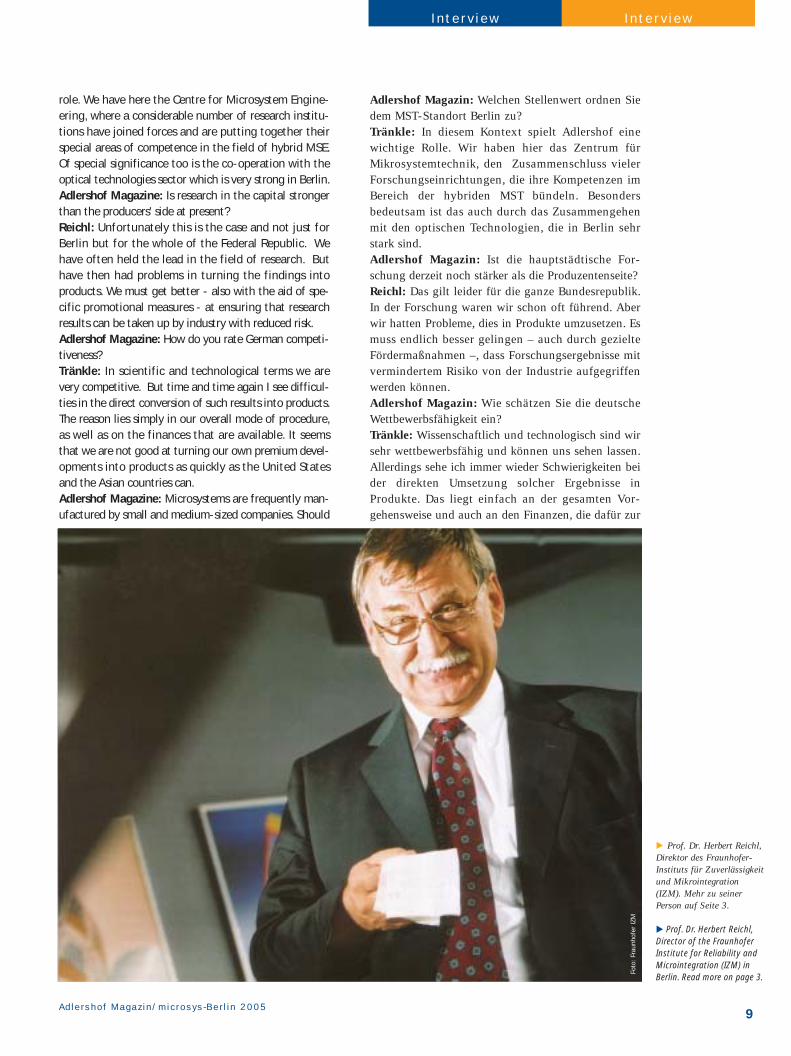
� Prof. Dr. Herbert Reichl,Direktor des Fraunhofer-Instituts für Zuverlässigkeitund Mikrointegration(IZM). Mehr zu seinerPerson auf Seite 3.
� Prof. Dr. Herbert Reichl,Director of the FraunhoferInstitute for Reliability andMicrointegration (IZM) inBerlin. Read more on page 3.
Foto
: Fr
aunh
ofer
IZM

Inter v iewInter v iew
Verfügung stehen. Es scheint uns nur schlecht zugelingen, eigene gute Entwicklungen ebenso zügigwie die Amerikaner und die Asiaten umsetzen zukönnen. Adlershof Magazin: Mikrosysteme werden vielfachvon kleinen und mittelständischen Betrieben gefer-tigt. Müssen sich Großunternehmen mehr um diesenoch junge Technologie kümmern?Reichl: Einige Großunternehmen setzen MST ein,besonders im Automobilbau. Leider ist aber zu beob-achten, dass neue Mikrosystementwicklungen, die vorallem für hochvolumige Anwendungen gedacht sind,hauptsächlich in die Produktion nach Fernost abwan-dern. Mitunter wollen das Kunden so. Aber insgesamtmuss man sagen, dass die Bedrohung, hochvolumigeMST allein in Fernost zu fertigen, immer mehrzunimmt. Adlershof Magazin: Verschenken wir als Wirtschafts-nation damit wichtige Chancen? Tränkle: Wir verschenken sicher Chancen. Viel liegtnatürlich am Geld, das bei uns nicht in der Ge-schwindigkeit zur Verfügung steht wie in denerwähnten Ländern. Aus meiner Sicht gibt es inDeutschland auch noch zu wenig Bereitschaft, Po-tenziale und Chancen gemeinsam zu erkennen und zunutzen. Die wissenschaftlichen und technologischenKompetenzen von Universitäten und Instituten müs-sen stärker mit den Möglichkeiten der Industriegebündelt werden. Wir sind dabei, das zu verbessern. Reichl: Die Projektförderung insbesondere durch denBund steigt nicht. Im Gegenteil, sie stagniert und soll-te wieder auf normales Niveau angehoben werden.Wünschenswert ist es, nicht nur die Entwicklung vonMST zu unterstützen, sondern auch die Umsetzungvon Forschungsergebnissen in Industrieprodukte zufördern. Wegen der Kosten können das Mittelständleroft nicht leisten. Allerdings sollte die Kooperation zwi-schen Instituten und Firmen insgesamt enger werden,und wir dürfen weder mutlos noch zu ungeduldig sein.
large enterprises concern themselves more with theseyoung technologies?Reichl: Certain large enterprises are using MSE for, inparticular, the automobile sector. Unfortunately we alsohave to observe that new microsystem developments -and in particular those that are envisaged for high vol-ume applications - emigrate to the Far East when itcomes to production. Sometimes this is what the cus-tomers want. But overall one has to say that the threatthat high-volume MSE products will be manufacturedsolely in the Far East is steadily growing.Adlershof Magazine: Are we as an industrial nationthereby throwing away important chances?Tränkle: We are certainly throwing away opportunities.Naturally it has a lot to do with money, with the factthat money is not made available with the speed that itis in the countries mentioned above. In my opinion thereis still too little readiness for the relevant parties to rec-ognize and utilize the areas with potential and opportu-nity. The scientific and technological fields of compe-tence of universities and institutes must be broughttogether better with the opportunities provided by theindustry. We are engaged in improving this situation.Reichl: The furthering of projects and in particular thefurthering of these by the Federal Government is notincreasing. On the contrary it has stagnated and shouldbe brought up to an appropriate level again. What isneeded is not just that microsystem engineering devel-opments are supported but that in addition the conver-sion of research results into industrial products is pro-moted. Often medium-sized firms are not able to man-age this on their own because of the costs. Neverthelessthe overall co-operation between institutes and firms isbecoming closer and we should neither give up hope norbecome too impatient.Adlershof Magazine: What positive effects does micro-sys-Berlin have on the city as a location?Reichl: Conference and trade fair promote dialogue not
Günther Tränkle hat 1988 an der Universität Stutt-gar t in Physik mit Arbeiten zu Quantisierungs- undVielteilcheneffekten in III/V Halbleiter-Strukturen pro-moviert. Ab 1988 leitete er am Walter-Schottky-Insti-tut der TU München die III/V-Halbleiter technologie.Von 1995 bis 1996 war er Abteilungsleiter am Fraun-hofer-Institut für Angewandte Festkörperphysik inFreiburg/Brsg. 1996 wurde er Direktor des Ferdi-nand-Braun-Instituts in Berlin. Seit 2002 ist er außer-dem Professor an der Technischen Universität Berlinfür das Fachgebiet Mikrowellentechnik und Optoelek-tronik. Seine derzeitigen Forschungsgebiete liegen inder III/V-Halbleitertechnologie, in der Mikro- und Milli-meterwellenelektronik sowie bei Hochleistungs-Diodenlasern.
Prof. Dr. Günther Tränkle received his doctorate(Ph.D.) in Physics at the University of Stuttgar t, in1988, where he specialized in quantisation and many-body ef fects in III/V quantum well structures. In1988, he joined the Walter-Schottky-Institute at the TUMunich, heading its III/V-semiconductor technologyand working on field-ef fect transistors and laserdiodes. From 1995 to 1996, he served as Depar t-ment Head at the Fraunhofer-Institute for AppliedSolid-State Physics in Freiburg, Germany. In 1996, hewas appointed Director of the Ferdinand-Braun-Institute in Berlin. Since 2002, he also holds a Chairon microwaves and optoelectronics at the TechnicalUniversity Berlin. His current research interestsinclude: III/V-semiconductor technology, micro- andmm-waves and high power diode lasers.
10 Ad le rshof Magaz in/mic rosys -Ber l in 2005

Adlershof Magazin: Welche Effekte bringt die mikro-sys-Berlin für den Standort?Reichl: Diese Messe fördert den Dialog zwischen denFirmen, aber auch zwischen Unternehmen undForschungseinrichtungen. Ich wünsche mir damit einstärkeres Zusammenarbeiten beispielsweise zwischender Kommunikations- und der MST-Industrie, so dasswir unsere Stärken noch weiter ausbauen können.Adlershof Magazin: Studien haben ein enormes
jährliches Wachstum des weltwei-ten MST-Marktes prognostiziert:2005 soll er demnach auf etwa 68Milliarden US-Dollar wachsen(1996: 14 Milliarden US-Dollar).Ist diese Entwicklung trotz derWirtschaftsflaute in Europa soeingetreten?Reichl: Auch in den Jahren, indenen es zu starken Einbrüchenbei den Halbleiterspeichern oderbei anderen Elektronikkomponen-ten kam, ist die Automobilelek-tronik gewachsen, und das giltebenso für die Sensorik. Es isttatsächlich festzustellen, dass derMarkt für Sensoren und andereMikrosysteme immer größer ge-worden ist, und ich glaube, dassdie Zahlen zutreffen. Die MST
dringt in nahezu alle Branchen vor; in Kürze wird esneue Anwendungen in der Nahrungsmittelkontrolle,in der Logistik, in der Verfahrenstechnik, in Biologieund Chemie geben. In manchen Branchen gilt schonjetzt: Wer marktfähig bleiben will, darf umMikrosysteme keinen Bogen machen. Automobilbau,Kommunikation und Medizin, das sind drei Bereiche,in denen Deutschland mit MST momentan an derSpitze ist. Adlershof Magazin: Was wird MST künftig bewirken?Tränkle: Grundsätzlich geht es bei Mikrosystem-technik immer darum, das Leben einfacher, dieLebensqualität besser und Menschen mobiler zumachen. Ein Beispiel aus dem FBH: Wir realisierenmit einer unserer Ausgründungen gerade eine ganzspezifische Laserdiode, ein kleines Lasersystem, dasspäter in GPS-Satelliten zur genauen Positionsbe-stimmung auf der Erde eingesetzt werden soll. Damitkönnen beispielsweise Handys bei einem Unfall auto-matisch den exakten Aufenthaltsort an die Rettungs-stelle durchgeben. Das neue Lasersystem ist außerdemkleiner, leistungsstärker und kostengünstiger als exi-stierende Systeme.Das Interview führte/The interview was conducted by
Thomas Wolter
only between firms but also between firms and researchinstitutions. Here I would like to see still greater co-operation between, for example, the communicationsindustry and the MSE industry so that we can build upour strengths still further.Adlershof Magazine: Studies have forecast an enormousannual growth for the world-wide MSE market:According to them it will grow to 68 billion US dollars by2005 (1996: 14 billion US dollars). Is the market inEurope also develop-ing in this way in spiteof the economic dol-drums here?Reichl: Even in theyears in which therewere sharp drops inthe semiconductormemories market aswell as in the marketfor other electroniccomponents, theautomobile electronicssector grew and thesame also held goodfor sensors. Indeed itcan be establishedthat the market forsensors and othermicrosystems has be-come larger all the time and I believe that the figuresalso hold good for Europe. MSE is penetrating into prac-tically every sector; in a short time there will be newapplications in the checking of food, in logistics, inprocess engineering, in biology and in chemistry. In somesectors it already holds good that each firm that wishesto remain competitive cannot afford not to get involvedin microsystems. Automobile construction, communica-tion and medicine - these are three fields in whichGermany is in the lead with MSE at the moment.Adlershof Magazine: What will MSE give us in thefuture?Tränkle: Fundamentally MSE will make life simpler,improve the quality of life still further and make us moremobile. One example from the Ferdinand-Braun Insti-tute: We are in the process of realizing with one of ourspin-offs a very specific laser diode - a small laser system- that will later be used in GPS satellites for precise posi-tioning on earth. If for example an accident occurs,mobile phones are able to inform the rescue centerautomatically about the exact location. In addition thenew laser system is significantly smaller, more powerfuland even cheaper than existing systems.
Inter v iewInter v iew
11Ad le rshof Magaz in/mic rosys -Ber l in 2005 11
Foto
: Fe
rdin
and-
Bra
un-In
stitu
t

Berufe
12 Ad le rshof Magaz in/mic rosys -Ber l in 2005
Jobs
Good training –secure jobsExperts are forecasting that the world-wide mar-ket for microsystem engineering (MSE) will doubleroughly every five years. In order to keep up withthis rapid rate of development, targeted further-ing of the up-and-coming generation is needed inGermany, not only in respect of graduates but alsoin respect of skilled workers.
We have a large requirement for excellentlytrained skilled workers", states Nicolas Hübener.He is the project manager of the MANO
(Microsystem Engineering Training in North-East Ger-many) network with its seat in Berlin Adlershof, presentlyone of six associated enterprises, co-financed by theGerman Ministry of Science and Education, distributedthroughout the Federal Republic which have set them-selves the task of improving the training and further-training opportunities in the area of this technology.
Hübener knows the facts: "MSE training started inGermany at the right time." At the start of the 90s - thefirst microsystems had already entered into the automo-bile sectors and had made the mobile telephone and CDplayer possible - full-time courses of study in microsystemengineering were initiated at universities in - amongstother places - Berlin and Regensburg. In 1998 courses ofapprenticeship leading to the profession of microsystemtechnician with the focal points of semiconductor andmicrosystem engineering started while medium-sizedcompanies in the capital as well as research institutionsjoined together into a training association. Gradually moreuniversities and institutions of higher education integrat-ed MSE as a secondary subject in their natural sciencecourses of study or at least started to offer lectures on thesubject.
Today there are twelve separate courses of study in MSEthroughout the Federal Republic including one at the
Gute Ausbildung –sichere ArbeitsplätzeExperten prognostizierten, dass sich der welt-weite Markt für Mikrosystemtechniken (MST)etwa alle fünf Jahre verdoppelt. Um diesesrasante Entwicklungstempo mitgehen zu kön-nen, bedarf es in Deutschland einer gezieltenNachwuchsförderung sowohl im akademischenals auch im Facharbeiterbereich.
Wir haben einen großen Bedarf an exzellentausgebildeten Fachkräften“, weiß NicolasHübener. Er ist Projektleiter des 2002 mit Sitz
in Adlershof gegründeten Netzwerkes MANO (Mikrosys-temtechnik Ausbildung in Nord-Ostdeutschland), einemvon bundesweit sechs BMBF-geförderten Netzwerken,die sich das Ziel gestellt haben, die Aus- und Weiter-bildung in dieser Zukunftstechnologie zu verbessern.
Hübener kennt die Fakten: „Die MST-Ausbildungbegann in Deutschland zur richtigen Zeit.“ Anfang der90er Jahre, die ersten Mikrosysteme hatten Einzuggehalten in den Automobilbau sowie das Handy undden CD-Player möglich gemacht, wurden Direktstu-diengänge Mikrosystemtechnik an Hochschulen etwa inBerlin und Regensburg eingerichtet. 1998 begann dieBerufsausbildung zum Mikrotechnologen mit denSchwerpunkten Halbleiter- und Mikrosystemtechnik,und mittelständische Betriebe der Hauptstadt sowieForschungseinrichtungen schlossen sich zu einemAusbildungsverbund zusammen. Nach und nach inte-grierten weitere Hochschulen MST als Nebenfach innaturwissenschaftliche Studienrichtungen oder botenzumindest solche Lehrveranstaltungen an.
Heute gibt es bundesweit zwölf eigenständige Stu-diengänge MST, darunter an der FH für Technik undWirtschaft in Berlin. Insgesamt etwa 2000 Studentenhaben bislang mit einem Diplom abgeschlossen. DieZahl der Hochschulen, die MST im Lehrprogrammhaben, schätzt Hübener auf inzwischen über 50. Rück-schläge, wie das gescheiterte Chipfabrik-Projekt inFrankfurt (Oder), lasten allerdings auf der Bilanz.„Dadurch mussten MST-Facharbeiterausbildungen, dieals anspruchsvoll und ingenieurnah gelten, abgebro-chen werden.“ Durch die Verlagerung großer Produk-tionsstätten hätten manche Standorte und Ausbildungs-zentren für junge Fachkräfte an Attraktivität verloren.„Generell aber gilt: Mehr als 80 Prozent der MST-Absolventen finden bereits im ersten Anlauf, oft schonim Studium, einen interessanten und gut bezahltenArbeitsplatz in der Forschung oder in der Industrie.Dabei zählt, dass sie gut auf die Praxis vorbereitet sind.“Bei den Mikrotechnologen, deren Lehre bald neu struk-turiert werden solle, sei es ähnlich, wirbt Hübener für
� Der MANO-Stand beider Veranstaltung „Fit für
Ausbildung“
� The MANO network pre-sents itself at a fair called
„Fit for Job Training“ Foto
: Ze
ns

BerufeJobs
University of Technology, Trade and Industry in Berlin. Upto the present time a total of some 2000 students havegraduated. The number of universities and colleges thatoffer studies in MSE is estimated by Hübener to be over50. Naturally setbacks such as the failure of the chip fac-tory project in Frankfurt (Oder) are a burden on the debitside. "As a result of the failure, courses of apprenticeshipleading to the profession of microsystem technician andwhich are rated demanding and industry-relevant, had tobe broken off.". Similarly the relocating of large produc-tion works caused a number of locations and training cen-tres for young skilled workers to lose their attractiveness."However in general it can be said that more than 80 % ofMSE graduates find an interesting and well-paid job inresearch or industry straightaway or often even in thecourse of their studies. What counts here is that they arewell prepared for practical work." The situation is similarwith the microsystem technicians, for whom the coursesof apprenticeship will shortly be restructured, reportsHübener for the growth sector MSE, which has its mostimportant centres in Baden-Württemberg, Bavaria, Berlin,Saxony and Thuringia.
An essential condition for the high quality of the train-ing is the close co-operation between educational institu-tions and firms, i.e. between university and vocationalschool areas, research and industry. At least 30 such part-ner enterprises based in Berlin, Bran-denburg and Mecklenburg-Vorpom-mern have come together in theMANO network in order to advancethe initial training offers and to intro-duce new forms of training. Quali-fication offers will also be developedand supra-regional exchanges withthe other networks will be promoted.
Exemplifying what is being done,two well-known institutions from thecapital, namely the Fraunhofer Insti-tute for Reliability and Micro-Inte-gration and the Ferdinand-Braun-Institut für Höchstfrequenztechnik,are active in this way for their ownup-and-coming generation. Todaynine institutions of higher educationfrom the MANO region have MSEcourses in their programme. "Fromthis spring on we will be offering anadditional advancement qualificationas certified MSE technician at theStaatliche Technikerschule (StateTechnicians School) in Berlin", reportsHübener. At the same time his area oftasks is also growing - MANO is takingover the role of speaker and therebythe co-ordinating function for all sixGerman MSE training networks.
die Wachstumsbranche, die ihre wichtigsten Kerne inBaden-Württemberg, Bayern, Berlin, Sachsen undThüringen hat.
Geradezu Bedingung für hohe Ausbildungsqualität istdie enge Kooperation von Institutionen und Firmen ausdem Hoch- und dem Berufsschulbereich, der Forschungund der Industrie. Gut 30 solcher Partner aus Berlin,Brandenburg und Mecklenburg-Vorpommern habensich im MANO-Netzwerk zusammengefunden, um so-wohl die Erstausbildung voranzutreiben und neue Aus-bildungsformen einzuführen als auch Qualifizierungs-angebote zu entwickeln und den überregionalen Aus-tausch mit den anderen Netzwerken zu fördern. Für deneigenen Nachwuchs engagieren sich auf diese Weisezum Beispiel zwei renommierte Institutionen aus derHauptstadt: das Fraunhofer-Institut für Zuverlässigkeitund Mikrointegration und das Ferdinand-Braun-Institutfür Höchstfrequenztechnik. Neun Hochschulen derMANO-Region haben MST mittlerweile im Lehrpro-gramm. „Ab diesem Frühjahr werden wir an der Staat-lichen Technikerschule in Berlin zudem eine Aufstiegs-qualifizierung zum staatlich geprüften MST-Technikeranbieten“, berichtet Hübener. Zeitgleich wächst auchsein Aufgabenbereich – MANO übernimmt die Sprecher-und damit die Koordinierungsfunktion für alle sechsdeutschen MST-Ausbildungsnetzwerke. Thomas Wolter
Ad le rshof Magaz in/mic rosys -Ber l in 2005 13
eagleyard Photonics Rasantes Wachstum mit innovativenHalbleiter-Laserdioden Technologieführer auf der Überholspur
Unsere Laserdioden sind die Kernkomponenten in innovativenLasersystemen für Medizin, Analytik, Industrie und Wissenschaft.Das eagleyard Team setzt wissenschaftliche Leistung in kunden-gerechte Produkte um. Mit dem Ferdinand-Braun-Institut habenwir dabei einen starken Partner, dessen Forschungsergebnisse aufdem Gebiet der Halbleiterlaser weltweit anerkannt sind.
www.eagleyard.com We focus on power .

14 Ad le rshof Magaz in/mic rosys -Ber l in 2005
Transfer Transfer
Orders from all overthe world The Anwenderzentrum für Mikrosystemtech-nik (AZM - Application Centre for MicroEngineering) at BESSY (Berliner Elektronen-speicherring-Gesellschaft für Synchrotron-strahlung) was completed in 2002. The appli-cation centre at Adlershof, which required aninvestment of 7,5 million Euro, has been oper-ated jointly since being opened by BESSY andthe Technical University of Berlin. "In themeantime it is working almost like an indus-trial undertaking and its capacity is nearlyfully utilized", reports Prof. Dr. WolfgangEberhardt, the Scientific Managing Director ofBESSY. "We are interested in working withfurther partners from the business worldwhich would like to carry out projects fromthe development stage through to fabricationin the user centre".
At AZM, which is in practice a laboratory centre forthe development of processes as well as a serviceprovider for companies from all over the world,
Aufträge aus allerWeltDas industrienahe Anwenderzentrum fürMikrosystemtechnik (AZM) bei BESSY, derBerliner Elektronenspeicherring-Gesellschaftfür Synchrotronstrahlung, war 2002 fertig ge-worden. Die 7,5-Millionen Euro-Investition inAdlershof, seither gemeinsam von BESSY undder Technischen Universität Berlin betrieben,arbeitet inzwischen fast wie ein Industrie-betrieb und ist weitgehend ausgelastet, berich-tet Prof. Dr. Wolfgang Eberhardt, der Wissen-schaftliche Geschäftsführer von BESSY. „Wirsind jedoch immer an weiteren Partnern ausder Wirtschaft interessiert, die im Anwender-zentrum Projekte von der Entwicklung bis zurFertigung durchführen wollen.“
Im AZM, praktisch ein Laborzentrum für dieProzessentwicklung sowie Dienstleister für Unter-nehmen aus aller Welt, werden Mikrokompo-
nenten, mikromechanische und -optische Bauteile ausMetallen oder Kunststoffen gefertigt, die hochpräziseund zum Teil unvorstellbar klein und mit dem bloßen
Aufträge aus aller WeltOrders from all over the world
Foto
: FB
H/S
chur
ian

Ad le rshof Magaz in/mic rosys -Ber l in 2005 15
TransferTransfer
Auge nicht mehr sichtbar sind:Ihre Größenordnungen erstreckensich vom Millimeter- bis in denNanometerbereich (MillionstelMillimeter). Nur mittels der imTeilchenbeschleuniger erzeugtenSynchrotronstrahlung und demlithographischen Direct-LIGA-Ver-fahren können solche Hightech-Bauteile mit der in der Mikrosys-temtechnik (MST) benötigten Prä-zision hergestellt werden. Dafürstehen dem AZM drei der 46Strahlrohre am Ring sowie mehre-re Reinräume und Labore zur Ver-fügung.
Nach den Worten WolfgangEberhardts hat das Anwenderzentrum inzwischen Fir-menaufträge unter anderem aus Deutschland, Japan,der Schweiz und Australien realisiert. Produziert wur-den winzige Zahnräder für Mikropositioniergetriebe,die zum Beispiel bei der Produktion von hochinte-grierten Leiterplatten eingesetzt werden, Holo-gramme, außerdem spezielle Prägestempel sowieOptikkomponenten. Die Kooperation mit Infineon undClariant führte zur Entwicklung neuer Fotolacke fürdie Chipherstellung. Für den Eigenbedarf von BESSY
micro-components, micro-mechanical and micro-opticalcomponents of metal or plastic are manufactured. Theparts are high-precision and in part unimaginably smalland invisible to the naked eye. Their sizes range from afew millimetres down to the nanometer range (mil-lionths of millimetres). Such high-tech components canonly be manufactured in the precision required for microengineering with the aid of the synchrotron radiationgenerated in the particles accelerator and the litho-graphic direct-LIGA technique. Available to AZM for thiswork are three of the 46 beamlines onthe ring as well as a number of cleanrooms and laboratories. According toEberhardt the application centre hasin the meantime carried out orders forcompanies based in - amongst othercountries - Germany, Japan, Switzer-land and Australia. The items thathave been produced include tiny gear-wheels for micro-positioning drives asused, for example, in the productionof PC boards, holograms, imprintingtools and optical components. Co-operation with Infineon and Clariantled to the development of new photoresists for the production of chips. Inaddition optics for X-ray microscopeshave been produced for BESSY's ownrequirements.
"The quantities being manufacturedin AZM are increasing. New ideas arecoming along all the time as to whatwe can do with our very good facili-ties and what new products and ser-vices we can offer", says the managingdirector. He foresees a future focalpoint for the application centre in theproduction of high-quality microsys-tem components of metal. "We are
Foto
: FO
EN X

TransferTransfer
get controlled ...motion control
“timing and speed ...”
www.micos.ws
IMPRESSUM/ IMPRINTHerausgeber/Publisher: WISTA-MANAGEMENT GMBH in Zusammen-arbeit mit der TSB Technologiestiftung Innovationsagentur Berlin GmbHund dem Zentrum für Mikrosystemtechnik Berlin (ZEMI)Verantwortlich/Responsible for the content: Dr. Peter Strunk Redaktion/Editorial Staff: Thomas Wolter, Josef Zens (CvD)Gesamtherstellung/Production: wbpr Public Relations,Berlin/Potsdam, www.wbpr.deAnzeigen/Advertising: wbpr, Enrico Schulze, Tel.: 0331/201 66 74Layout: Gregor Wollenweber, Löning Werbeagentur,www.loening-werbeagentur.deDruck/Printing: Druckerei Arnold, GroßbeerenÜbersetzungen/Translation: lost in translation? SprachenserviceGunhild BlankensteinTitelbild: FOEN X PhotostudioRedaktionsadresse/Address: WISTA-MANAGEMENT GMBH, BereichKommunikation, Rudower Chaussee 17, 12489 Berlin, Tel.: 030/63 92 22 25, Fax: 030/63 92 21 99, E-Mail:[email protected], Internet: www.adlershof.de; www.wista.deNamentlich gekennzeichnete Beiträge stellen nicht unbedingt dieMeinung der Redaktion dar. Nachdruck von Beiträgen mitQuellenangaben gestattet. Belegexemplar erbeten.Contributions, which are personally signed, do not necessarily repre-sent the opinion of the editorship. Reproduction of articles with sour-ce specification permitted. Copy requested.Erscheinungsdatum/Date of Publication: 07.03. 2005
wurden Optiken für Röntgenmikroskope hergestellt.„Die Fertigungsmengen im AZM steigen. Es gibtbeständig neue Ideen, was wir dort mit unseren gutenMöglichkeiten machen und zusätzlich anbieten kön-nen“, sagt der Geschäftsführer. Einen künftigenSchwerpunkt für das Anwenderzentrum sieht er in derProduktion hochwertiger Mikrosystem-Komponentenaus Metallen. „Wir sind an weiteren Partnern aus derWirtschaft interessiert, die im AnwenderzentrumProjekte von der Entwicklung bis zur Fertigungdurchführen wollen“, bekräftigt Eberhardt.
Engen Kontakt pflegt BESSY auch mit Standort-partnern in Adlershof, so zum Ferdinand-Braun-Institut für Höchstfrequenztechnik (FBH). Es hattejüngst ein neuartiges Hochleistungs-Lasersystem vor-gestellt, das gemeinsam mit dem AZM entwickeltworden ist. Der „Master Oszillator Power Amplifier“(MOPA), knapp so groß wie ein Fingernagel, ist etwazweitausend Mal leistungsfähiger als ein Laserpointerund kann beispielsweise in der Spektroskopie und inder Datenübertragung eingesetzt werden. DasBesondere des Systems: Die drei winzigen Kom-ponenten des Lichterzeugers – eine Laserdiode, eineGlaslinse sowie ein leistungsfähiger Trapezverstärker– werden mit einer bislang unerreichten Genauigkeitexakt hintereinander auf einer mikrooptischen Bankaus Silizium positioniert. Dieses Bauteil mit seinensehr kleinen Strukturen und speziellen Metallkompo-nenten zur Befestigung der Systemteile werden imAnwenderzentrum mit Hilfe der Synchrotronstrah-lung und des LIGA-Verfahrens erzeugt. „Die nurwenige Millimeter lange und breite Siliziumbankermöglicht und erfordert eine Positioniergenauigkeitvon nur einem Tausendstel Millimeter und ist damiteine wichtige Voraussetzung für die hochpräziseFertigung dieser leistungsstarken neuen Halbleiter-Lasereinheiten“, betont Eberhardt. Thomas Wolter
interested in working with further partners from thebusiness world which would like to carry out projectsfrom the development stage through to fabrication inthe AZM", underlines Eberhardt.
BESSY also maintains close contacts with partners whoare also located at Adlershof, for example with theFerdinand-Braun-Institut für Höchstfrequenztechnik(FBH). This institute has recently presented an innovativehigh-performance laser system, which was developedjointly with AZM. The "Master Oscillator PowerAmplifier" (MOPA) - just the size of a finger nail - issome two thousand times more powerful than a laserpointer and can be used for example in spectroscopy andthe transmission of data. The special feature of the sys-tem: The three tiny components of the light generator,namely a laser diode, a glass lens and a powerful trape-zoidal amplifier are positioned with a precision neverachieved previously exactly one behind the other on amicro-optical bench of silicon. The latter componentwith its very small structures and special metal parts forfixing the system components is produced in the AZMwith the aid of synchrotron radiation and the LIGA tech-nique. "The silicon bench, which is just a few millimetreslong and wide, makes possible and requires a positioningprecision of just one thousandth of a millimetre and thusrepresents an important precondition for the highly pre-cise fabrication of these powerful new semiconductorlaser units", emphasizes Eberhardt.
� Prof. Dr. WolfgangEberhardt, Wissen-
schaftlicher Geschäfts-führer von BESSY
� Prof. Dr. WolfgangEberhardt, Scientific
Managing Director ofBESSY Fo
to: El
ke W
eiss
/TU
-Ber
lin

Ad le rshof Magaz in/mic rosys -Ber l in 2005 17
Adlershof in ZahlenSTADT FÜR WISSENSCHAFT, WIRTSCHAFT UND MEDIEN
FLÄCHE: 420 ha
BESCHÄFTIGTE: ca. 11.000
UNTERNEHMEN: 658
WISSENSCHAFTS- UND TECHNOLOGIEPARK
INVESTITIONEN
Geplant (1991 - 2007): 2,5 - 3 Mrd. EUR
ENTWICKLUNGSSTAND
Neuansiedlungen 2004: 62 Unternehmen
Umsätze der Unternehmen (einschließlich Fördermit-
tel) und Budgets der wissenschaftlichen Einrichtungen
(einschließlich Drittmittel) 2004: 554 Mio. EUR
UNTERNEHMEN
375 Unternehmen
Zahl der Mitarbeiter: 3.580
WISSENSCHAFTLICHE EINRICHTUNGEN
12 außeruniversitäre Forschungseinrichtungen, 1.500
Mitarbeiter, darunter 672 Wissenschaftler, zuzüglich
130 Doktoranden und Gäste
HUMBOLDT-UNIVERSITÄT ZU BERLIN
6 naturwissenschaftliche Institute (Institut für Infor-
matik, Mathematik, Chemie, Physik, Geographie und
für Psychologie), 130 Professoren, ca. 7000 Studen-
ten und 900 sonstige Mitarbeiter
MEDIENSTADT
127 Unternehmen, ca. 900 Mitarbeiter
GEWERBE
156 Unternehmen, ca. 4.000 Mitarbeiter
LANDSCHAFTSPARK
66 Hektar
Adlershof in figuresCITY OF SCIENCE, TECHNOLOGY AND MEDIA
AREA: 420 hectares (1,040 acres)
STAFF: approx. 11,000
ENTERPRISES: 658
SCIENCE AND TECHNOLOGY PARK
INVESTMENTS
scheduled (1991 - 2007): EUR 2.5 - 3 billion
STATUS OF DEVELOPMENT
New settlements 2004: 62 companies
Turnover of the companies and funds
of the scientific institutes (2004): EUR 554 million
COMPANIES
375 innovative companies
Staff: 3,580
SCIENTIFIC INSTITUTIONS
12 non-university research institutes with around 1,500
employees, among them 672 scientists as well as 130
doctorate students and guests
HUMBOLDT UNIVERSITY OF BERLIN
6 natural science institutes (Institutes for Computer
Science, Mathematics, Chemistry, Physics, Geography
and Psychology), 130 professors, approx. 7,000 students
and 900 other staff
MEDIA CITY
127 companies, approx. 900 staff
INDUSTRIAL ESTATE
156 companies, approx. 4,000 staff
LANDSCAPE PARK
66 hectares
Foto
: FO
EN X
