voltage, current, and temperature monitoring for solar
TRANSCRIPT

Copyright © 2016, Texas Instruments Incorporated
CC2538
LM5017
AMP
±
+
AMP±
+
PV IN +
PV IN ±
PV OUT +
PV OUT ±
RF ANT
1TIDUCM3–December 2016Submit Documentation Feedback
Copyright © 2016, Texas Instruments Incorporated
Voltage, Current, and Temperature Monitoring for Solar Module Level PowerElectronics
TI DesignsVoltage, Current, and Temperature Monitoring for SolarModule Level Power Electronics
DescriptionThis verified reference design provides an overview onhow to implement a solar module level monitoring andcommunication subsystem. This TI Design addressesthe key need of a highly cost-optimized monitoring andcommunication subsystem for solar module levelpower electronics (MLPE). This design showcases ahighly integrated solution for accurate voltage, current,and temperature monitoring along with ZigBee®communication using the CC2538 to enable solarmodule level monitoring.
Resources
TIDA-00640 Design FolderCC2538 Product FolderLM5017 Product FolderTLV342A Product Folder
ASK Our E2E Experts
Features• <2% Error Voltage Measurement• <2% Error Current Measurement• CC2538 M3 SoC for ZigBee Communication• PCB Based Antenna With Simplified Filtering
Circuitry
Applications• Solar Energy Monitoring and Communications
An IMPORTANT NOTICE at the end of this TI reference design addresses authorized use, intellectual property matters and otherimportant disclaimers and information.

Copyright © 2016, Texas Instruments Incorporated
CC2538
LM5017
AMP
±
+
AMP±
+
PV IN +
PV IN ±
PV OUT +
PV OUT ±
RF ANT
System Overview www.ti.com
2 TIDUCM3–December 2016Submit Documentation Feedback
Copyright © 2016, Texas Instruments Incorporated
Voltage, Current, and Temperature Monitoring for Solar Module Level PowerElectronics
1 System Overview
1.1 System DescriptionModule level power electronics (MLPEs) provide a very granular method of optimizing a solar system.Moving the maximum power point tracking (MPPT) or other power management services to the modulereduces the cost overhead on a system and enables a higher total system power output. However, itremoves some of the capability of monitoring string degradation because every module appears toperform optimally to an outside observer. The addition of integrated power measurement at each MLPEenables several additional features:• Array performance metrics to evaluate instillation return on investment• Mesh based power point tracking more efficient power conversion• Module degradation information due to aging or soiling• Module mismatch and instillation issue analysis
The TIDA-00640 integrates the voltage, current, and temperature measurement into a single system thatis able to be powered by the module itself and wireless communicate the data back to a central pointthrough a number of wireless standards. This TI Design enables quick integration of the measurement andwireless technology with MPLEs to make a full distributed power conversion system.
1.2 Key System Specifications
Table 1. Key System Specifications
PARAMETER SPECIFICATIONS DETAILSVoltage Input 10- to 90-V input voltage support for modern HV modules Section 2.1Sensor type Shunt resistor Section 2.2Current measurement accuracy <2% calibrated and uncalibrated error full scale Section 4.2Voltage measurement accuracy <2% calibrated and <2.5% uncalibrated error full scale Section 4.1Temperature measurement ±5°C Section 2.6Wireless functionality 1 minute of no motion detected Section 2.5
1.3 Block Diagram
Figure 1. TIDA-00640 System Block Diagram
128KB/256KB/512KB Flash
16KB Retention SRAM
16KB Standard SRAM
4KB ROM
ARMCortexTM
± M3
32 MHz
JTAG
SWO
NVIC
MPU
2 UARTS
2 SSI/SPI
SE
RIA
L IN
TE
RF
AC
ES
USB Full-SpeedDevice
I2C
SY
ST
EM
Systick Timer
Timer/PWM/CCP4x (32 bit or 2x16 bit)
Watchdog Timer
32 GPIO
32-ch DMA
32-MHz XTAL and 16-MHz RC Oscillator
32-kHz XTAL and 32-kHz RC Oscillator
32-bit Sleep Timer
IEE
E 8
02.1
5.4
RA
DIO
Packet-Handling Processor
Command-Strobe Processor
MAC Timer
RF Chain
Modulator
Syn
th
TX
RX
Demod
SE
CU
RIT
Y AES-128/256SHA-256
ECCRSA-2048
DE
BU
G
INT
ER
FA
CE
cJTAG/JTAG
ICEPick
AN
ALO
G
LDO RegulatorPower-on Reset and Brown-
Out Detection
Low-Power Comparator
8-ch 12-bit ADCWith Temp Sensor
Copyright © 2016, Texas Instruments Incorporated
www.ti.com System Overview
3TIDUCM3–December 2016Submit Documentation Feedback
Copyright © 2016, Texas Instruments Incorporated
Voltage, Current, and Temperature Monitoring for Solar Module Level PowerElectronics
1.4 Highlighted Products
1.4.1 CC2538
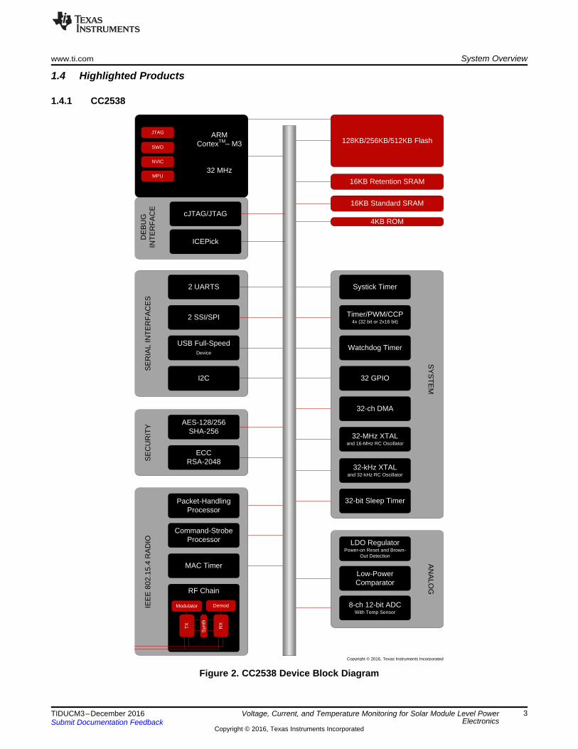
Figure 2. CC2538 Device Block Diagram
System Overview www.ti.com
4 TIDUCM3–December 2016Submit Documentation Feedback
Copyright © 2016, Texas Instruments Incorporated
Voltage, Current, and Temperature Monitoring for Solar Module Level PowerElectronics
• Microcontroller– Powerful ARM® Cortex®-M3 with Code Prefetch– Up to 32-MHz clock speed– 512KB, 256KB, or 128KB of in-system-programmable flash– Supports on-chip over-the-air upgrade (OTA)– Supports dual ZigBee application profiles– Up to 32KB of RAM (16KB with retention in all power modes)– cJTAG and JTAG debugging
• RF– 2.4-GHz IEEE 802.15.4 compliant RF transceiver– Excellent receiver sensitivity of –97 dBm– Robustness to interference with ACR of 44 dB– Programmable output power up to 7 dBm
• Security hardware acceleration– Future proof AES-128/256, SHA2 hardware encryption engine– Optional: ECC-128/256, RSA hardware acceleration engine for secure key exchange– Radio command strobe processor and packet handling processor for low-level MAC Functionality
• Low power– Active-Mode RX (CPU Idle): 20 mA– Active-Mode TX at 0 dBm (CPU Idle): 24 mA– Power Mode 1 (4-µs Wake-Up, 32-KB RAM retention, full register retention): 0.6 mA– Power Mode 2 (sleep timer running, 16-KB RAM retention, configuration register retention): 1.3 µA– Power Mode 3 (external interrupts, 16-KB RAM retention, configuration register retention): 0.4 µA– Wide supply-voltage range (2 to 3.6 V)
• Peripherals– µDMA– 4× general-purpose timers (each 32-bit or 2× 16-bit)– 32-bit 32-kHz sleep timer– 12-bit ADC with eight channels and configurable resolution– Battery monitor and temperature sensor– USB 2.0 full-speed device (12 Mbps)– 2× SPI– 2× UART– I2C– 32 general-purpose I/O pins (28 × 4 mA, 4 × 20 mA)– Watchdog timer
• Layout– 8-mm × 8-mm QFN56 package– Robust device for industrial operation up to 125°C– Few external components– Only a single crystal needed for asynchronous networks
+
+
+
VINBST
RON
RTN
SW
VCC
FB
VIN
VOUT
RFB1
RC
RUV1
RON
COUT
CBST
CIN
RFB2
RUV2
L1
UVLO
+
CVCC
LM50177.5 to 100 V
1
2
3
4
5
6
8
7
SD
Copyright © 2016, Texas Instruments Incorporated
www.ti.com System Overview
5TIDUCM3–December 2016Submit Documentation Feedback
Copyright © 2016, Texas Instruments Incorporated
Voltage, Current, and Temperature Monitoring for Solar Module Level PowerElectronics
• Development tools– CC2538 development kit– Reference design certified under FCC and ETSI regulations– Full software support for Contiki/6LoWPAN, smart grid, lighting, and ZigBee home automation with
sample applications and reference designs available– Code Composer Studio™– IAR Embedded Workbench® for ARM– SmartRF™ Studio– SmartRF Flash Programmer
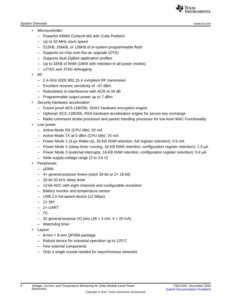
1.4.2 LM5017
Figure 3. LM5017 Typical Application
• Wide 7.5- to 100-V input range• Integrated 100-V high-side, and low-side switches• No Schottky required• Constant on-time control• No loop compensation required• Ultra-fast transient response• Nearly constant operating frequency• Intelligent peak current limit• Adjustable output voltage from 1.225 V• Precision 2% feedback reference• Frequency adjustable to 1 MHz• Adjustable undervoltage lockout (UVLO)• Remote shutdown• Thermal shutdown
Vsup+
+VOUT
RF
VIN
RI
Vsup-
Copyright © 2016, Texas Instruments Incorporated
System Overview www.ti.com
6 TIDUCM3–December 2016Submit Documentation Feedback
Copyright © 2016, Texas Instruments Incorporated
Voltage, Current, and Temperature Monitoring for Solar Module Level PowerElectronics
1.4.3 TLV342A
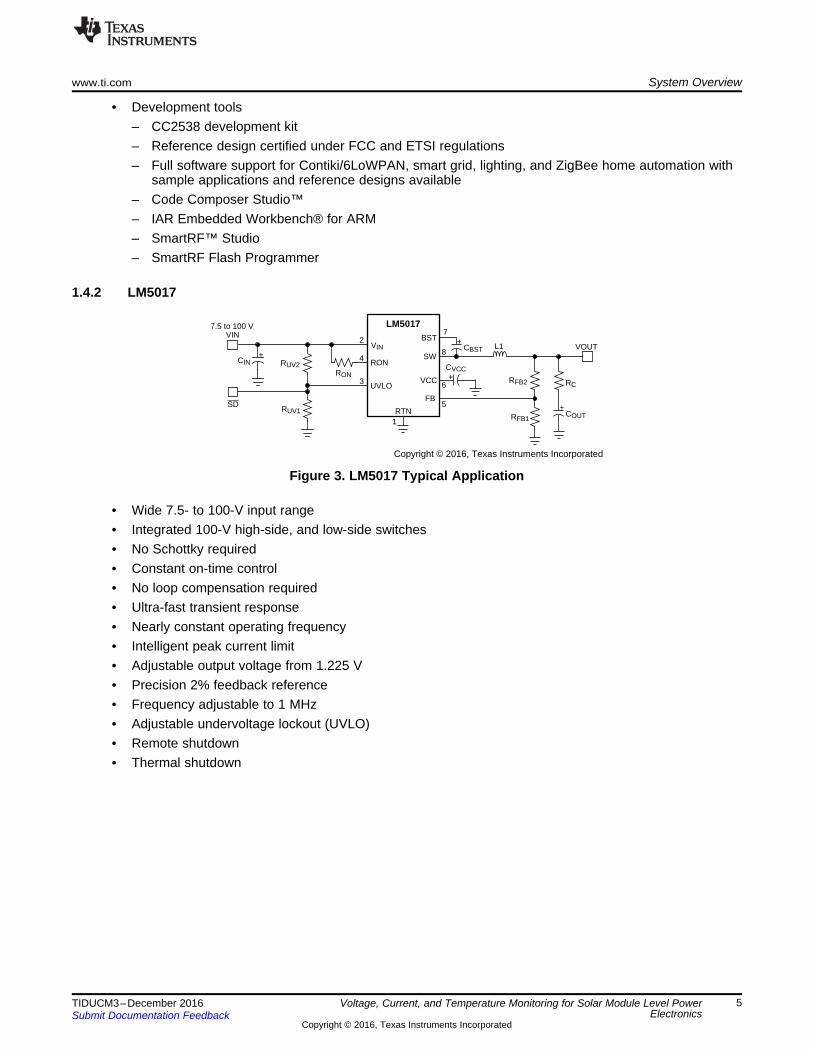
Figure 4. TLV342A Typical Application
• 1.8- and 5-V performance• Low offset (A Grade)
– 1.25 mV maximum (25°C)– 1.7 mV maximum (–40°C to 125°C)
• Rail-to-rail output swing• Wide common-mode input voltage range: –0.2 V to (V+ – 0.5 V)• Input bias current: 1 pA (typical)• Input offset voltage: 0.3 mV (typical)• Low supply current: 70 µA/channel• Low shutdown current: 10 pA (typical) per channel• Gain bandwidth: 2.3 MHz (typical)• Slew rate: 0.9 V/µs (typical)• Turnon time from shutdown: 5 µs (typical)• Input referred voltage noise (at 10 kHz): 20 nV/√Hz• ESD protection exceeds JESD 22
– 2000-V human-body model (HBM)– 750-V charged-device model (CDM)
Shunt power dissipation 0.100 W% power loss from shunt 1 00 100 0.03%
Maximum module power 300 W= ´ = ´ =
www.ti.com System Design Theory
7TIDUCM3–December 2016Submit Documentation Feedback
Copyright © 2016, Texas Instruments Incorporated
Voltage, Current, and Temperature Monitoring for Solar Module Level PowerElectronics
2 System Design Theory
2.1 Power InputThe intent of this TI Design is to be fully powered by the solar module from which it is measuring power.Modern solar modules are increasing in voltage in order to produce a higher power output without theneed to scale the current passing capabilities. At the time writing, common solar modules have a nominalvoltage rating in the mid 70 V and power output capabilities in excess of 300 W. These values are onlyexpected to increase as the solar cell technology advances.
To satisfy the growing input voltage requirements of solar cells, the TIDA-00640 is specified with a verywide input voltage of up to 90 V. This is accomplished with the LM5017 step-down regulator, which iscapable of handling input voltages from 7.5 to 100 V. This range is very well suited to the dynamic natureof PV modules, which can have wide voltage output swings dependent of current illuminance andtemperature. It enables very high step-down voltages, from the 90-V input, to the 3.3 V required for theVCC in this TI Design.
The LM5017 contains internal switches with switch current handling of 600 mA. The total current draw ofthe system at its VCC rail is expected to be < 200 mA, even when transmitting, which is well within theoutput range of the LM5017 even at lower efficiency operation points. Being this far below the maxoperating current will also keep any self-heating to a minimum.
To keep the system cost and complexity low for the TIDA-00640, a type 1 configuration from the LM5017datasheet was chosen. Find additional information on designing power stages using this configuration inthe LM5017 datasheet[1]. If a more stable VCC is required, then a type 3 configuration can beimplemented, but does add additional components to the power stage. This could be desirable to generatea more stable VREF for the analog sensing circuitry.
A final consideration in the power stage is the type of components selected. In most switch mode powerstages, a large electrolytic capacitor is used on the input to reduce input voltage ripple. This is undesirablein this design for two major reasons:1. An electrolytic capacitor rated for 200-V would be physically large2. Electrolytic capacitors are not desirable for MLPEs due to their short lifespans in wide temperature
environments
To mitigate these issues, the input capacitance from the standard design was replaced with a ceramictype able to handle the voltage, and by nature, be more stable in higher temperature environments
2.2 Current MeasurementThe primary goals of the current measurement feature in the TIDA-00640 are to minimize impact on thesolar string and to provide reasonable accuracy. Because all of the modules in a solar string are typicallyplaced in series, the current measurement must be able to support the entire string’s output current. If theTIDA-00640 is intended to be placed at the input of an MLPE module and not the output, then only thesingle module’s current needs to be accounted for because the MLPE will be passing the string current.Parallel module arrangements also result in a lower module current requirement. A current of 10 A waschosen as a maximum current capacity of the sense system; however, this could easily be resized to allowfor more current or higher sensing accuracy.
A low-value current shunt resistor was chosen as the sensor in this TI Design to keep system complexityand cost to a minimum. This design uses a low-side sense element to reduce the need for high-voltagetranslation typical of a high-side element. Because the system is self-contained, this has no impact on therest of the solar system beyond the minute power loss of the now series resistor.
Shunt resistors can provide their own complications; however, due to self-heating and power dissipationrequirements. To this end, a limit of 100 mW was placed on the shunt. On a typical 300-W module, thisresults in a negligible power loss as shown in Equation 1:
(1)

122 x
x 32273.3 2.6
= ® =
INV 10 A 0.001 261 2.6 V= ´ W ´ =
OUTV I R 10 A 0.001m 0.01 V= ´ = ´ W =
System Design Theory www.ti.com
8 TIDUCM3–December 2016Submit Documentation Feedback
Copyright © 2016, Texas Instruments Incorporated
Voltage, Current, and Temperature Monitoring for Solar Module Level PowerElectronics
The 1-mΩ shunt resistor is rated to 1% tolerance and 170 ppm. This shunt resistor was chosen with costin mind. The ppm rating was lowered to a practical level for an MLPE, which operates in the upper rangeof 60⁰C to 85⁰C. To use a cost competitive shunt resistor, the tolerance was minimized at 1%. The shuntresistor’s tolerance can be improved at the expense of component price or ppm rating. The shuntresistor’s 1% tolerance equates to variances in board-to-board sensing accuracy, but it can be calibratedout.
A 1-mΩ shunt resistor at 10 A has a voltage output determined by Ohm's law as:(2)
The TIDA-00640 uses the built-in ADC on the CC2538 for measurement. This is a 12-bit ADC with aninput voltage range of 0 to VREF. VREF is selectable in software to be either an internal 1.15 V, or use anexternal reference attached to the VDD5 pin. To maintain a high dynamic range, the external VREF waschosen for this TI Design and is attached to the board’s VCC rail at 3.3 V. This provides an effective inputrange of 0 to 3.3 V. To ensure linearity and no saturation in the design, an upper limit of the voltage inputwas chose to be closer to 2.5 V.
The amplification circuit must then bring the 0.01 V of the shunt at 10 A to 3 V for the ADC. This is anormal gain of 300. To provide some additional overhead, a gain of only 260 will be used. This is achievedwith a simple non-inverting amplifier configured with a 1.15-kΩ and 300-kΩ resistor in the feedbacknetwork. With this configuration, the final ADC input voltage at 10 A would be:
(3)
This input voltage can be correlated with VREF, and the maximum ADC value (which is equivalent to VREF)to determine the usable ADC range, and what the expected granularity is to validate that the design will besufficient.
(4)
The value of 3227 is about 80% the full range of the ADC, as well as approximately what is expected at afull 10-A input. This also correlates to approximately 3 mA per ADC count, which is sufficient granularityfor this TI Design, and well below the error expected to be injected from other sources.
In this simple implementation of a shunt-based current sense solution, there are several potential sourcesof error. The primary source is the potential for drift and offset in the amplifier. The specifications of theoperation amplifier could be narrowed at the expense of system cost using a higher precision device likethe OPA333 or a dedicated shunt amplifier such as the INA216.
The second primary source of error is the passive device tolerances. 1% devices were used across thesystem, which could lead to stacking of error and contribute to board to board variances of severalpercent. Tighter tolerance devices can be used to help increase board-to-board accuracy when using thesame calibration constants.
2.3 Voltage MeasurementThe TIDA-00640 uses a simple voltage divider and amplifier configuration to measure the module levelvoltage. A low upper limit was set to give the analog circuitry plenty of overhead in the case of higher thanexpected module voltage output. A divider of 50.8 was setup to bring the input of the amplifier at the full90-V range down to 1.77 V. This 90-V range is specific to this board and can be reduced if the targetsystem has a lower operating voltage, and more granularity is needed.
The voltage sensing divider feeds a simple buffer amplifier, which shares a package with the currentsensing amplifier. As in the current measurement system, a VREF of 3.3 will be used on the ADC of theCC2538. The slightly lower max input voltage limits the maximum ADC output to 2197; however, this stillresults in a granularity of 40 mV, or 0.0044% of full range, which is significantly beyond the requirementsfor this TI Design.
In order to minimize the power loss in the divider, high values resistors were used. A total drop of 510 kΩresults in only 177 µA of current draw from the module. Resistors with reasonably low temperaturecoefficient of 100 ppm and 1% tolerance were chosen to keep board-to-board variance and temperaturedrift low without sacrificing cost tolerance. Tighter specifications could be used for this analog front-end ifrequired.
R421
Antenna
(50 )Ω
C371
C381C382
C372
C373
L372
L381
C561
Power supply decoupling capacitors are not shown
Digital I/O not connected
2.0- to 3.6-V power supply
3.3-V power supply
C31 C21
R31
R21
R32
D+
D-
XT
AL
C441
C451
Optional 32-kHz crystal
XTAL
C341 C351
5 PB0
1 DGND_USB
2 USB_P
3 USB_N
4 DVDD_USB
CC2538DIE ATTACH PAD:
10 VDD
9 PC4
8 PC5
7 PC6
6 PC7
R_BIAS 42
AVDD 41
AVDD 40
AVDD 39
RF_N 38
AVDD 33
XOSC32M_Q1 34
XOSC32M_Q2 35
AVDD 36
RF_P 37
PD3 29
PD4 30
PD5 31
DCOUPL2 32
14 PC0
13 PC1
12 PC2
11 PC3
RE
SE
T_
N2
8
PD
227
PD
126
PD
025
VD
D24
VD
D15
PA
420
PA
521
PA
622
PA
723
PA
016
PA
117
PA
218
PA
319
DC
OU
PL
56
DV
DD
55
PB
154
PB
253
PB
352
JTA
G_T
CK
47
PB
748
PB
649
PB
550
PB
451
AV
DD
_G
UA
RD
43
PD
6/X
OS
C32
K_Q
144
PD
7/X
OS
C32
K_Q
245
JT
AG
_T
MS
46
C321
C281
RESET_N
R281
L373
L374
2 nH
1.2 pF
3.3 nH
Copyright © 2016, Texas Instruments Incorporated
www.ti.com System Design Theory
9TIDUCM3–December 2016Submit Documentation Feedback
Copyright © 2016, Texas Instruments Incorporated
Voltage, Current, and Temperature Monitoring for Solar Module Level PowerElectronics
Two resistors were used on the high-voltage side of the divider to distribute the 90 V across multipleelements. If one of the resistors did happen to fail into a short state, the second resistors will be able toact as a failsafe to prevent the entire MPLE system from potentially failing from too much voltage beingapplied to the sensing circuitry.
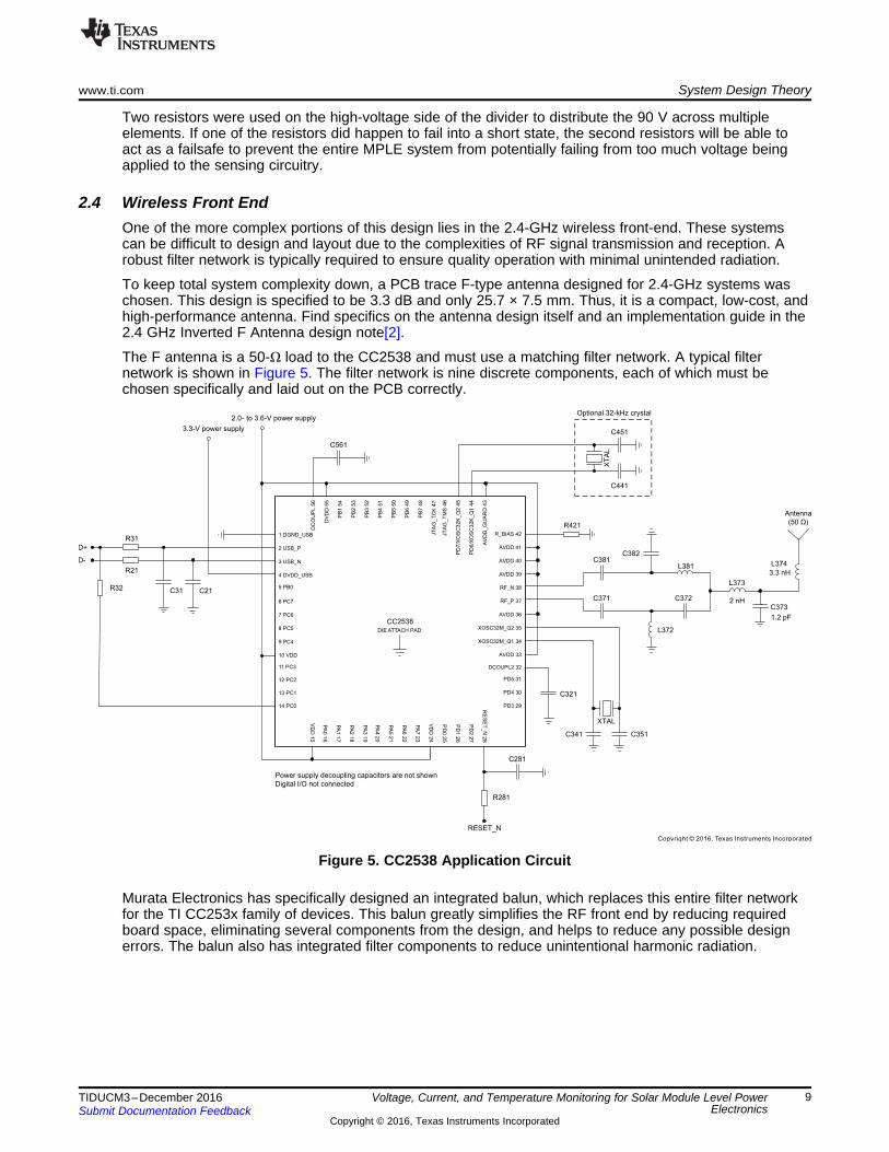
2.4 Wireless Front EndOne of the more complex portions of this design lies in the 2.4-GHz wireless front-end. These systemscan be difficult to design and layout due to the complexities of RF signal transmission and reception. Arobust filter network is typically required to ensure quality operation with minimal unintended radiation.
To keep total system complexity down, a PCB trace F-type antenna designed for 2.4-GHz systems waschosen. This design is specified to be 3.3 dB and only 25.7 × 7.5 mm. Thus, it is a compact, low-cost, andhigh-performance antenna. Find specifics on the antenna design itself and an implementation guide in the2.4 GHz Inverted F Antenna design note[2].
The F antenna is a 50-Ω load to the CC2538 and must use a matching filter network. A typical filternetwork is shown in Figure 5. The filter network is nine discrete components, each of which must bechosen specifically and laid out on the PCB correctly.
Figure 5. CC2538 Application Circuit
Murata Electronics has specifically designed an integrated balun, which replaces this entire filter networkfor the TI CC253x family of devices. This balun greatly simplifies the RF front end by reducing requiredboard space, eliminating several components from the design, and helps to reduce any possible designerrors. The balun also has integrated filter components to reduce unintentional harmonic radiation.

1 2 3
E1
Unbalance Port1
GND2
Balance Port3
GND6
GND5
Balance Port4
FL1
GND0
R2
R_BIAS42
PA723
XOSC32M_Q235
JTAG_TMS46
JTAG_TCK47
PA622
RF_P37
RF_N38
RESET_N28
XOSC32M_Q134
USB_P2
USB_N3
GND
OSC32M1
OSC32M2
TMSTCK
56.0k
R1
GND
S_CURS_VIN GND
1000pFC23
2.2k
R13
GND
RESET
DNPC15
DNPC14
GNDGND
RF_PRF_N
Copyright © 2016, Texas Instruments Incorporated
System Design Theory www.ti.com
10 TIDUCM3–December 2016Submit Documentation Feedback
Copyright © 2016, Texas Instruments Incorporated
Voltage, Current, and Temperature Monitoring for Solar Module Level PowerElectronics
The final schematic of the RF front end is shown in Figure 6. The additional components on the output ofthe filter were used as placeholders for potential balancing needed in the design, but were not changed.The design operates as is with C14 and C15 being DNP, and R2 as a 0-Ω shunt.
Figure 6. TIDA-00640 RF Front End
Additional information regarding the usage of the Murata balun, including design practices, guidelines, andmeasured performance characteristics is available in the device's application note[3].

Coordinator
Router
End device
www.ti.com System Design Theory
11TIDUCM3–December 2016Submit Documentation Feedback
Copyright © 2016, Texas Instruments Incorporated
Voltage, Current, and Temperature Monitoring for Solar Module Level PowerElectronics
2.5 Wireless ProtocolThe TI CC2538 is a full SoC with an integrated IEEE 802.15.4 wireless radio. As such, the protocolsupport comes from the software stack chosen by the end user. At the time of publication, there are threemajor stacks fully supported on the platform: ZigBee PRO/2.0, ZigBee 3.0, and Contiki. The first two aredeveloped by TI and can be certified by the ZigBee foundation, and the third is an open source 6LowPanwireless operating system.
ZigBee technology is supported by the ZigBee Alliance to ensure interoperability between varioushardware and stacks from different manufacturers. The technology is designed to be a simpler and lessexpensive alternative to other wireless protocols on the market. ZigBee also enables sleepy devices forlow power consumption while still having transmission distances from 10 to 100 meters. Additionalnetwork size can be achieved by implementing a mesh network. The mesh topology lends itself well to asolar module instillation because a large geographic area can be covered without the need for acentralized router, to which all end nodes would need to connect.
A typical mesh network is made of a single coordinator device, and then many routers and end devices.The data transmitted from one device will intelligently propagate through the network until it reaches itsdestination; typically, an edge router capable of translating the ZigBee data to a higher throughputinterface such as Ethernet or Wi-Fi®. An example of a ZigBee mesh can be seen in Figure 7.
Figure 7. Mesh Network Layout
The CC2538 supports the ZigBee 2.0 specification through the Z-Stack software. This stack supports fullIPv6, 128-bit security keys, and over 400 simultaneous nodes on the network. ZigBee 2.0 is divided intoseveral application specific branches depending on the specific end device use case, including homeautomation, lighting, and smart energy. Additional information regarding Z-Stack and the ZigBee 2.0implementation can be found on the software product page (http://www.ti.com/tool/z-stack). However, withthe latest release, it is recommended to use ZigBee 3.0, which is backwards compatible with the 2.0specification.
ZigBee 3.0 is an evolution of the ZigBee 2.0 specification that does away with the application layer specificprotocols and moves to a single standard. This updated protocol is supported through the latest 3.0release of TI Z-Stack and includes several key features beyond the profile unification including improvedsecurity features, seamless low power connection states, and full backwards compatibility with the olderspecifications. The latest version of Z-Stack is available at http://www.ti.com/tool/z-stack.
System Design Theory www.ti.com
12 TIDUCM3–December 2016Submit Documentation Feedback
Copyright © 2016, Texas Instruments Incorporated
Voltage, Current, and Temperature Monitoring for Solar Module Level PowerElectronics
A third option is Contiki, which is an open source operating system for internet of things devices. Itsupports full IPv6 mesh, along with 6lowpan, RPL, and CoAP—all within a very small memory footprint.Additional information regarding Contiki as a whole is available from the project website(http://www.contiki-os.org/) and the TI implementation from the TI wiki: www.ti.com/contiki-6lowpan-wiki.
2.6 Temperature SensorThe temperature sensing functionality of the TIDA-00649 is derivative of the internal analog temperaturesensor in the CC2538 rather than using a discrete sensor. This internal sensor is specified to be accurateto ±10°C with no calibration or ±5°C with just a single-point calibration, which could easily be done atprograming time during production.
The typical use case of a temperature sensor in a solar application is to derate power electronics in theevent of the system crossing an over temp threshold. For that application, a more accurate remote sensorwould be more applicable. With the built-in sensor on the CC2538, the design is able to self-monitorsystem level temperature at the module level rather than at the power conversion electronics. This datacan then be used as part of a larger system level performance monitoring system.
Solar module efficiency is negatively related to module temperature or as the temperature drops theefficiency increases. Solar modules are general specified at 25°C. As the temperature increases abovethis point, the output current will rise, but the voltage output will drop faster, resulting in a decreasedpower output. As the temperature drops below 25°C, the inverse occurs. In extreme situations, the modulecould operate at up to 140% of the rated normal output.
Keeping track of the temperature can provide significant additional information regarding how a module isexpected to perform versus how it is actually performing. This data helps end users understand how thearray is aging and know if there are any potential problems that need to be remedied to maintain fulloutput performance. For this generic metric, the guaranteed ±5°C of the internal CC2538 temperature isdetermined to be sufficient. If a tighter specification for system temperature monitoring is required, TI’sarray of pre-calibrated silicon based sensors enable an easy upgrade path.

Copyright © 2016, Texas Instruments Incorporated
TIDA-00640100-V/10-A
PSU
Multimeter(Voltage)
Variable DC Load
Multimeter(Current)
TIDA-00640(RX)
PC
Voltage input
Voltage output
Voltage output
Voltage inputUART interfaceCurrent shunt
TLV342A AFE
CC2538 debug interface
LM5017 power supply
Wireless front end
CC2538 wireless SoC
www.ti.com Getting Started Hardware
13TIDUCM3–December 2016Submit Documentation Feedback
Copyright © 2016, Texas Instruments Incorporated
Voltage, Current, and Temperature Monitoring for Solar Module Level PowerElectronics
3 Getting Started Hardware
3.1 Hardware
Figure 8. Hardware Overview
3.2 Test Setup
Figure 9. Current and Voltage Accuracy Test Setup
To fully test the design characteristics of the TIDA-00640, a power supply, DC load, and several calibratedmeters were used. Because the design will be exposed to non-isolated high voltages, the RF capabilitywas used to transmit raw ADC readings from both current and voltage channels to a receive deviceconnected to a PC. The receive device was connected through J5 using a simple UART to USB serialbridge and read to a terminal window at 115200 baud.

Getting Started Hardware www.ti.com
14 TIDUCM3–December 2016Submit Documentation Feedback
Copyright © 2016, Texas Instruments Incorporated
Voltage, Current, and Temperature Monitoring for Solar Module Level PowerElectronics
The wireless stack used here is Contiki because it provided a simple interface, but has no bearing on themeasurement accuracy. A custom sensor was designed based on the example Contiki application, whichprovides the raw sample data to the application layer. This sensor uses AVDD5 as the voltage referenceand has a decimation rate of 512 to achieve the full 12-bit ENOB of the CC2538’s onboard ADC. Thesame measurement scheme could easily be implemented in the other supported stacks. This 12-bit rangewas also scaled by eight by the Contiki stack to make some of the data structures more homogeneousacross various libraries.
The variable DC load used is Kikusui PLZ15W, which is capable of 120-V DC, 10 A, and 150 W. Becauseit is not capable of sinking the full 1000 W that the board could measure, the voltage and currentmeasurements need to be performed independently.
Two multimeters were used to enable simultaneous measurement of both current and voltage, whichsimplifies the testing procedure. For the voltage measurement, a Keithley 2001 series meter was placed inparallel with the design. A 10-A capable multimeter is required for the current measurement, so an AgilentU3401A meter was used in series.
Due to the same full power limitations in the DC load, two power supplies were required to be used togenerate the full range 90-V and 10-A test scenarios. For the voltage test, a Xantrex XTR 100-8.5 sourcewas used and a Sorensen DLM 60-10 was used for the current.
The final test setup used in the TI lab is shown in Figure 9. The TIDA-00640 under test is placed inside aninterlocked enclosure to prevent accidental contact with the high voltage in the system. TI ESH guidelinesplace the exposed voltage limit at 50-V DC, but this may be different at other test sites. Use caution andfollow local regulations regarding high-voltage electronics.
Figure 10. TIDA-00640 Test Setup

ADC Reading
Act
ual V
olta
ge
0 5000 10000 15000 200000
10
20
30
40
50
60
70
80
90
100
D001
Average ReadingLinear (Average Reading)
( )2
Input voltage V 0.005 ADC reading 0.2543
R 0.9999
= ´ +
=
www.ti.com Testing and Results
15TIDUCM3–December 2016Submit Documentation Feedback
Copyright © 2016, Texas Instruments Incorporated
Voltage, Current, and Temperature Monitoring for Solar Module Level PowerElectronics
4 Testing and Results
4.1 Voltage Accuracy TestingFor voltage testing, the primary board input was used. This both powered the board under test and servedas the measured value. As such, the lowest value able to be measured was approximately 6.3 V due tothe input dropout voltage of the onboard power supply. The input voltage was measured to four significantfigures, which is less than the 12-bit accuracy of the ADC, but accurate enough to ensure that the designfalls within our designed accuracy specification and granularity.
A reference board was used to get a baseline of the relationship between applied voltage versus ADCmeasurement. Eighteen discrete samples were taken for this data set, each approximately 5 V apart in the6- to 90-V range. For each voltage point, several ADC measurements were recorded to help determinehow much deviation can be seen in the reading. Using a basic linear correlation, Equation 5 wasdeveloped to describe the relationship:
(5)
Figure 11. Voltage versus ADC Linearity
Voltage (V)
Err
or
6.3 12.8 19.3 25.8 32.3 38.8 45.3 51.8 58.3 64.8 71.3 77.8 84.3 90.4-2.0%
-1.5%
-1.0%
-0.5%
0.0
0.5%
1.0%
D002
Error LowError HighError Average
Testing and Results www.ti.com
16 TIDUCM3–December 2016Submit Documentation Feedback
Copyright © 2016, Texas Instruments Incorporated
Voltage, Current, and Temperature Monitoring for Solar Module Level PowerElectronics
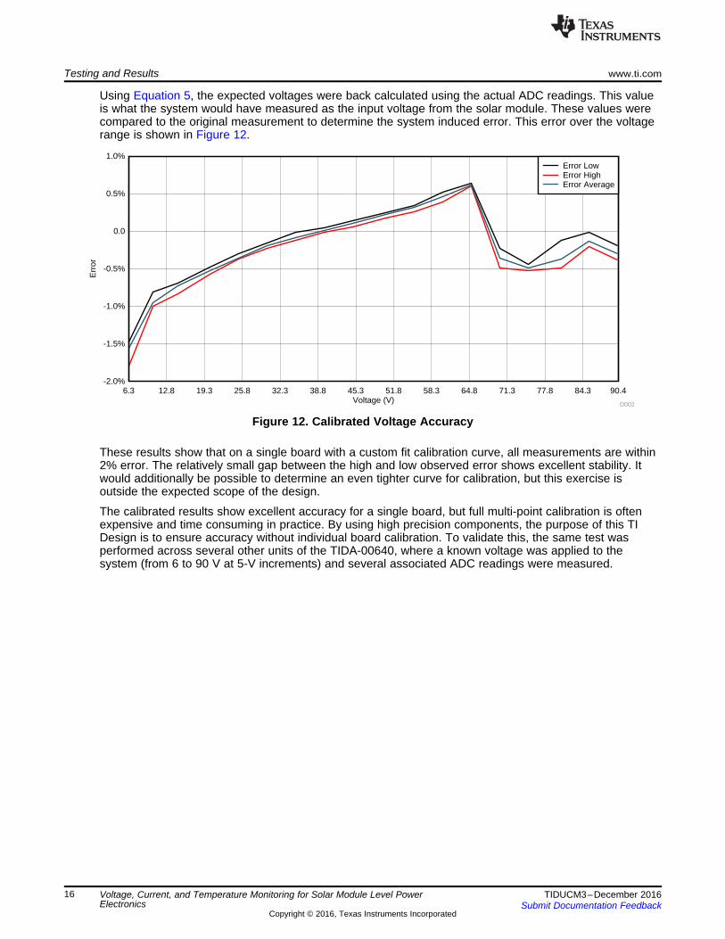
Using Equation 5, the expected voltages were back calculated using the actual ADC readings. This valueis what the system would have measured as the input voltage from the solar module. These values werecompared to the original measurement to determine the system induced error. This error over the voltagerange is shown in Figure 12.
Figure 12. Calibrated Voltage Accuracy
These results show that on a single board with a custom fit calibration curve, all measurements are within2% error. The relatively small gap between the high and low observed error shows excellent stability. Itwould additionally be possible to determine an even tighter curve for calibration, but this exercise isoutside the expected scope of the design.
The calibrated results show excellent accuracy for a single board, but full multi-point calibration is oftenexpensive and time consuming in practice. By using high precision components, the purpose of this TIDesign is to ensure accuracy without individual board calibration. To validate this, the same test wasperformed across several other units of the TIDA-00640, where a known voltage was applied to thesystem (from 6 to 90 V at 5-V increments) and several associated ADC readings were measured.
Voltage (V)
Err
or
6.3 12.8 19.3 25.8 32.3 38.8 45.3 51.8 58.3 64.8 71.3 77.8 84.3 90.4-0.6%
-0.4%
-0.2%
0.0
0.2%
0.4%
0.6%
0.8%
1.0%
1.2%
D003
Error LowError HighError Average
www.ti.com Testing and Results
17TIDUCM3–December 2016Submit Documentation Feedback
Copyright © 2016, Texas Instruments Incorporated
Voltage, Current, and Temperature Monitoring for Solar Module Level PowerElectronics
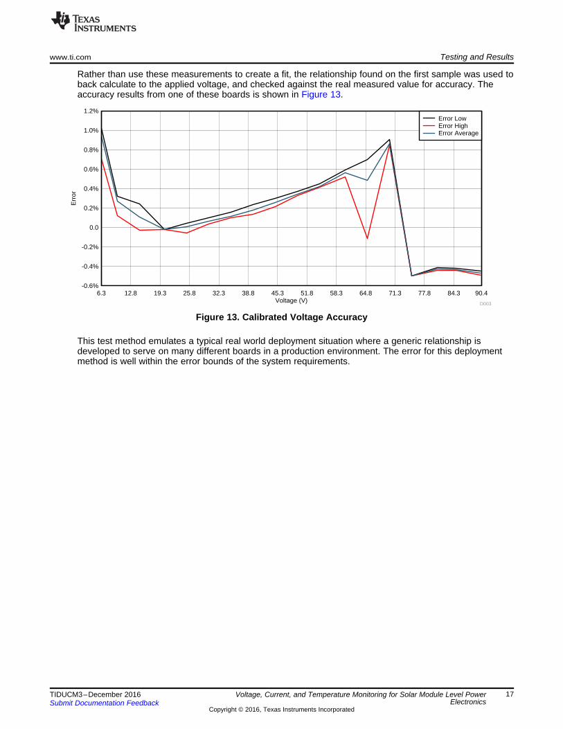
Rather than use these measurements to create a fit, the relationship found on the first sample was used toback calculate to the applied voltage, and checked against the real measured value for accuracy. Theaccuracy results from one of these boards is shown in Figure 13.
Figure 13. Calibrated Voltage Accuracy
This test method emulates a typical real world deployment situation where a generic relationship isdeveloped to serve on many different boards in a production environment. The error for this deploymentmethod is well within the error bounds of the system requirements.

ADC Reading
Act
ual V
olta
ge
-5000 0 5000 10000 15000 20000 25000 300000
2
4
6
8
10
12
D004
Average ReadingLinear (Average Reading)
( )2
Input current A 0.0003695 ADC reading 0.0458
R 0.9999
= ´ +
=
Testing and Results www.ti.com
18 TIDUCM3–December 2016Submit Documentation Feedback
Copyright © 2016, Texas Instruments Incorporated
Voltage, Current, and Temperature Monitoring for Solar Module Level PowerElectronics
4.2 Current Accuracy TestingThe current accuracy testing followed a similar procedure to the voltage testing. The board under test waspowered through the primary input, and current was sourced from the board output using a variableprogrammable load. While under operation, the board was powered by the primary input as well, so anominal voltage of 12 V was applied. This simulated a real world use scenario as close as possible withthe whole system being under test. Full power could not be accurately tested due to limitations in thetesting equipment, but because the measured signal is rather benign, there is little impact from the voltagemeasurement onto the current.
The reference board under test had a range of voltages applied, from 100 mA to 10 A, with steps ofapproximately 500 mA. For each current set point, several ADC readings were measured through thewireless link to determine stability. The current was measured with a multimeter with at least four digits ofaccuracy. The resultant data was used to extrapolate a linear fit to provide a mathematical relationshipbetween the ADC reading and real current. For the reference board, this relationship was found to be:
(6)
Figure 14. Current Linearity
Current (A)
Err
or
0.0 1.0 2.0 3.0 4.0 5.0 6.0 7.0 8.0 9.0 10.00.0
5.0%
10.0%
15.0%
20.0%
25.0%
30.0%
35.0%
40.0%
D006
Error LowError HighError Average
Voltage (V)
Err
or
0.1 1.1 2.1 3.1 4.1 5.1 6.1 7.1 8.1 9.1 10.0-0.2%
0.0
0.2%
0.4%
0.6%
0.8%
1.0%
1.2%
1.4%
1.6%
D005
Error LowError HighError Average
www.ti.com Testing and Results
19TIDUCM3–December 2016Submit Documentation Feedback
Copyright © 2016, Texas Instruments Incorporated
Voltage, Current, and Temperature Monitoring for Solar Module Level PowerElectronics
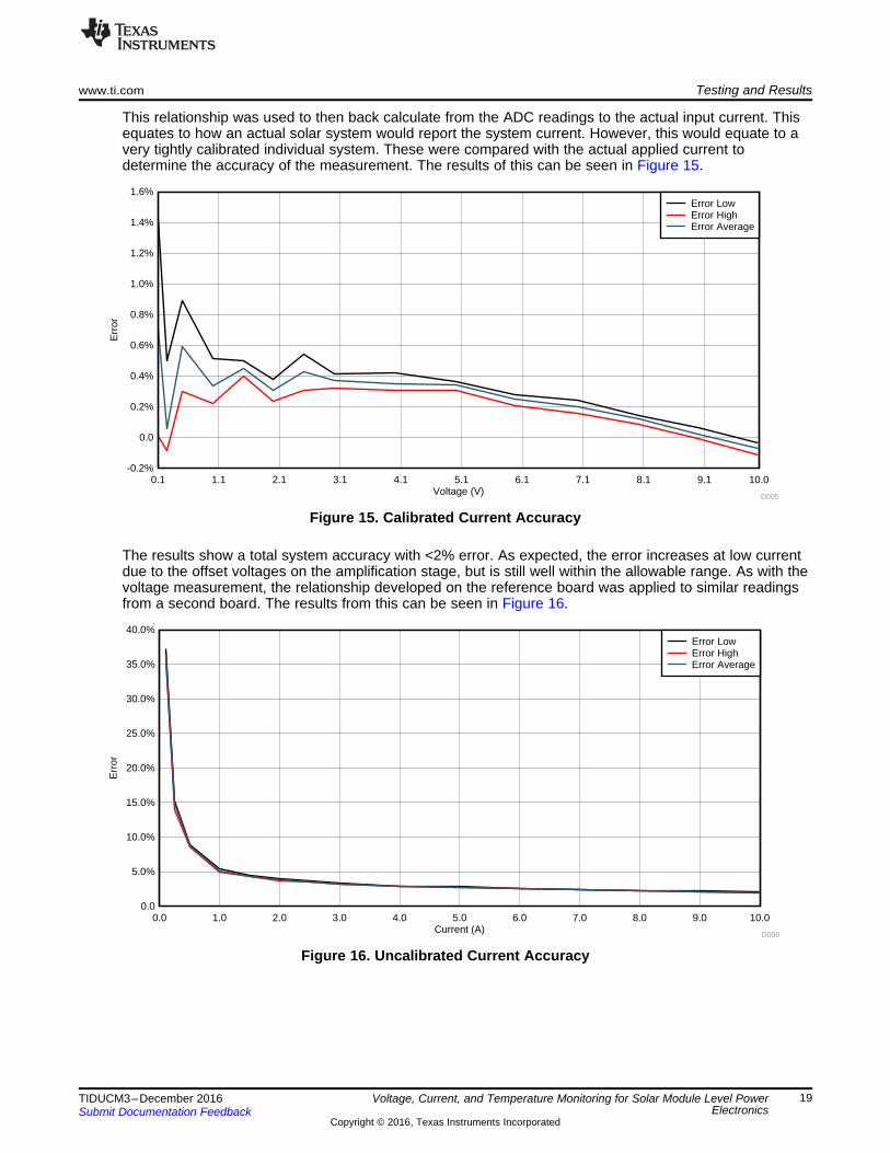
This relationship was used to then back calculate from the ADC readings to the actual input current. Thisequates to how an actual solar system would report the system current. However, this would equate to avery tightly calibrated individual system. These were compared with the actual applied current todetermine the accuracy of the measurement. The results of this can be seen in Figure 15.
Figure 15. Calibrated Current Accuracy
The results show a total system accuracy with <2% error. As expected, the error increases at low currentdue to the offset voltages on the amplification stage, but is still well within the allowable range. As with thevoltage measurement, the relationship developed on the reference board was applied to similar readingsfrom a second board. The results from this can be seen in Figure 16.
Figure 16. Uncalibrated Current Accuracy
Current (A)
Err
or
0.0 1.0 2.0 3.0 4.0 5.0 6.0 7.0 8.0 9.0 10.0-3.0%
-2.5%
-2.0%
-1.5%
-1.0%
-0.5%
0.0
0.5%
1.0%
1.5%
2.0%
2.5%
D007
Error LowError HighError Average
( ) ( )Input current A 0.0003695 ADC Reading 90 0.0458= ´ + +
Testing and Results www.ti.com
20 TIDUCM3–December 2016Submit Documentation Feedback
Copyright © 2016, Texas Instruments Incorporated
Voltage, Current, and Temperature Monitoring for Solar Module Level PowerElectronics
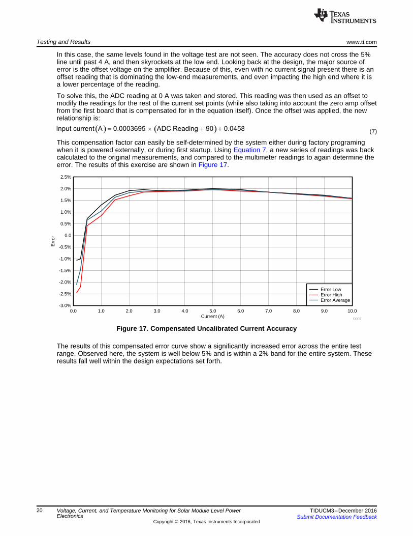
In this case, the same levels found in the voltage test are not seen. The accuracy does not cross the 5%line until past 4 A, and then skyrockets at the low end. Looking back at the design, the major source oferror is the offset voltage on the amplifier. Because of this, even with no current signal present there is anoffset reading that is dominating the low-end measurements, and even impacting the high end where it isa lower percentage of the reading.
To solve this, the ADC reading at 0 A was taken and stored. This reading was then used as an offset tomodify the readings for the rest of the current set points (while also taking into account the zero amp offsetfrom the first board that is compensated for in the equation itself). Once the offset was applied, the newrelationship is:
(7)
This compensation factor can easily be self-determined by the system either during factory programingwhen it is powered externally, or during first startup. Using Equation 7, a new series of readings was backcalculated to the original measurements, and compared to the multimeter readings to again determine theerror. The results of this exercise are shown in Figure 17.
Figure 17. Compensated Uncalibrated Current Accuracy
The results of this compensated error curve show a significantly increased error across the entire testrange. Observed here, the system is well below 5% and is within a 2% band for the entire system. Theseresults fall well within the design expectations set forth.
www.ti.com Design Files
21TIDUCM3–December 2016Submit Documentation Feedback
Copyright © 2016, Texas Instruments Incorporated
Voltage, Current, and Temperature Monitoring for Solar Module Level PowerElectronics
5 Design Files
5.1 SchematicsTo download the schematics, see the design files at TIDA-00640.
5.2 Bill of MaterialsTo download the bill of materials (BOM), see the design files at TIDA-00640.
5.3 Layout PrintsTo download the layer plots, see the design files at TIDA-00640.
5.4 Altium ProjectTo download the Altium project files, see the design files at TIDA-00640.
5.5 Gerber FilesTo download the Gerber files, see the design files at TIDA-00640.
5.6 Assembly DrawingsTo download the assembly drawings, see the design files at TIDA-00640.
6 Related Documentation
1. Texas Instruments, 100-V, 600-mA Constant On-Time Synchronous Buck Regulator, LM5017Datasheet (SNVS783)
2. Texas Instruments, 2.4 GHz Inverted F Antenna, Design Note DN0007 (SWRU120)3. Texas Instruments, Murata Balun for CC253x and CC254x LFB182G45BG2D280, Application Note
AN107 (SWRA380)
6.1 TrademarksAll trademarks are the property of their respective owners.
7 About the AuthorBART BASILE is a systems architect in the Texas Instruments Grid Infrastructure Solutions Team,focusing on renewable energy and EV infrastructure. Bart works across multiple product families andtechnologies to leverage the best solutions possible for system level application design. Bart received hisbachelors of science in electronic engineering from Texas A&M University.

IMPORTANT NOTICE FOR TI REFERENCE DESIGNS
Texas Instruments Incorporated (‘TI”) reference designs are solely intended to assist designers (“Designer(s)”) who are developing systemsthat incorporate TI products. TI has not conducted any testing other than that specifically described in the published documentation for aparticular reference design.TI’s provision of reference designs and any other technical, applications or design advice, quality characterization, reliability data or otherinformation or services does not expand or otherwise alter TI’s applicable published warranties or warranty disclaimers for TI products, andno additional obligations or liabilities arise from TI providing such reference designs or other items.TI reserves the right to make corrections, enhancements, improvements and other changes to its reference designs and other items.Designer understands and agrees that Designer remains responsible for using its independent analysis, evaluation and judgment indesigning Designer’s systems and products, and has full and exclusive responsibility to assure the safety of its products and compliance ofits products (and of all TI products used in or for such Designer’s products) with all applicable regulations, laws and other applicablerequirements. Designer represents that, with respect to its applications, it has all the necessary expertise to create and implementsafeguards that (1) anticipate dangerous consequences of failures, (2) monitor failures and their consequences, and (3) lessen thelikelihood of failures that might cause harm and take appropriate actions. Designer agrees that prior to using or distributing any systemsthat include TI products, Designer will thoroughly test such systems and the functionality of such TI products as used in such systems.Designer may not use any TI products in life-critical medical equipment unless authorized officers of the parties have executed a specialcontract specifically governing such use. Life-critical medical equipment is medical equipment where failure of such equipment would causeserious bodily injury or death (e.g., life support, pacemakers, defibrillators, heart pumps, neurostimulators, and implantables). Suchequipment includes, without limitation, all medical devices identified by the U.S. Food and Drug Administration as Class III devices andequivalent classifications outside the U.S.Designers are authorized to use, copy and modify any individual TI reference design only in connection with the development of endproducts that include the TI product(s) identified in that reference design. HOWEVER, NO OTHER LICENSE, EXPRESS OR IMPLIED, BYESTOPPEL OR OTHERWISE TO ANY OTHER TI INTELLECTUAL PROPERTY RIGHT, AND NO LICENSE TO ANY TECHNOLOGY ORINTELLECTUAL PROPERTY RIGHT OF TI OR ANY THIRD PARTY IS GRANTED HEREIN, including but not limited to any patent right,copyright, mask work right, or other intellectual property right relating to any combination, machine, or process in which TI products orservices are used. Information published by TI regarding third-party products or services does not constitute a license to use such productsor services, or a warranty or endorsement thereof. Use of the reference design or other items described above may require a license from athird party under the patents or other intellectual property of the third party, or a license from TI under the patents or other intellectualproperty of TI.TI REFERENCE DESIGNS AND OTHER ITEMS DESCRIBED ABOVE ARE PROVIDED “AS IS” AND WITH ALL FAULTS. TI DISCLAIMSALL OTHER WARRANTIES OR REPRESENTATIONS, EXPRESS OR IMPLIED, REGARDING THE REFERENCE DESIGNS OR USE OFTHE REFERENCE DESIGNS, INCLUDING BUT NOT LIMITED TO ACCURACY OR COMPLETENESS, TITLE, ANY EPIDEMIC FAILUREWARRANTY AND ANY IMPLIED WARRANTIES OF MERCHANTABILITY, FITNESS FOR A PARTICULAR PURPOSE, AND NON-INFRINGEMENT OF ANY THIRD PARTY INTELLECTUAL PROPERTY RIGHTS.TI SHALL NOT BE LIABLE FOR AND SHALL NOT DEFEND OR INDEMNIFY DESIGNERS AGAINST ANY CLAIM, INCLUDING BUT NOTLIMITED TO ANY INFRINGEMENT CLAIM THAT RELATES TO OR IS BASED ON ANY COMBINATION OF PRODUCTS ASDESCRIBED IN A TI REFERENCE DESIGN OR OTHERWISE. IN NO EVENT SHALL TI BE LIABLE FOR ANY ACTUAL, DIRECT,SPECIAL, COLLATERAL, INDIRECT, PUNITIVE, INCIDENTAL, CONSEQUENTIAL OR EXEMPLARY DAMAGES IN CONNECTION WITHOR ARISING OUT OF THE REFERENCE DESIGNS OR USE OF THE REFERENCE DESIGNS, AND REGARDLESS OF WHETHER TIHAS BEEN ADVISED OF THE POSSIBILITY OF SUCH DAMAGES.TI’s standard terms of sale for semiconductor products (http://www.ti.com/sc/docs/stdterms.htm) apply to the sale of packaged integratedcircuit products. Additional terms may apply to the use or sale of other types of TI products and services.Designer will fully indemnify TI and its representatives against any damages, costs, losses, and/or liabilities arising out of Designer’s non-compliance with the terms and provisions of this Notice.IMPORTANT NOTICE
Mailing Address: Texas Instruments, Post Office Box 655303, Dallas, Texas 75265Copyright © 2016, Texas Instruments Incorporated