vol. 4, issue 4, april 2015 performance analysis and ... · performance analysis and comparison of...
TRANSCRIPT

ISSN (Print) : 2320 – 3765
ISSN (Online): 2278 – 8875
International Journal of Advanced Research in Electrical,
Electronics and Instrumentation Engineering
(An ISO 3297: 2007 Certified Organization)
Vol. 4, Issue 4, April 2015
Copyright to IJAREEIE 10.15662/ijareeie.2015.0404104 2297
Performance Analysis and Comparison of
Conventional and Interleaved DC/DC Boost
Converter Using MULTISIM
Sandeep K Waghmare1, Amruta S Deshpande
2
PG Student, Dept. of Instrumentation & Control, College of Engineering, Pune, Maharashtra, India 1
Assistant Professor, Dept. of Instrumentation & Control, College of Engineering, Pune, Maharashtra, India 2
ABSTRACT: Step up conversion is widely used in many applications such as Electric vehicles, Photovoltaic (PV)
system, Uninterruptible power supplies (UPS) and fuel cell system. This paper shows simulation of conventionaland
interleaveddc-dc boost converter using NI MULTISIM software. Theseconvertersare tested by varying the input
voltage with constant duty cycle in Continuous Conduction Mode (CCM). The performance parameters of both the
converters are compared. Control of these converters is done by switching signals having fixed switching
frequency.Using interleaved converter we can reduced ripple at output voltageand output current.
KEYWORDS: NI MULTISIM, Conventional Boost Converter, Interleaved Boost converter, Ripple voltage, Ripple
current.
I. INTRODUCTION
For power electronic interfaces in renewable energy sources such as photovoltaic power systems and fuel cells DC-
DC converters are more important components. Main disadvantage of these renewable sources is that they give low
voltage output and thus needs booster in order to provide enough output voltage. Thus Interleaved Boost converter is a
solution for such a systems, which can give high step up voltage having smaller ripple to the output voltage and output
current. Also there is low switching loss for this circuit having faster transient response. Interleaved boost converter is
made up of two identical boost conversion units with an auxiliary inductor. Both the active power switches of this
converter can turn on at zero voltage due to this there is reduction in their switching losses which increases the
conversion efficiency. Operation analysis and design of the converter becomes quite simple as both the parallel
operated boost conversion units are identical.
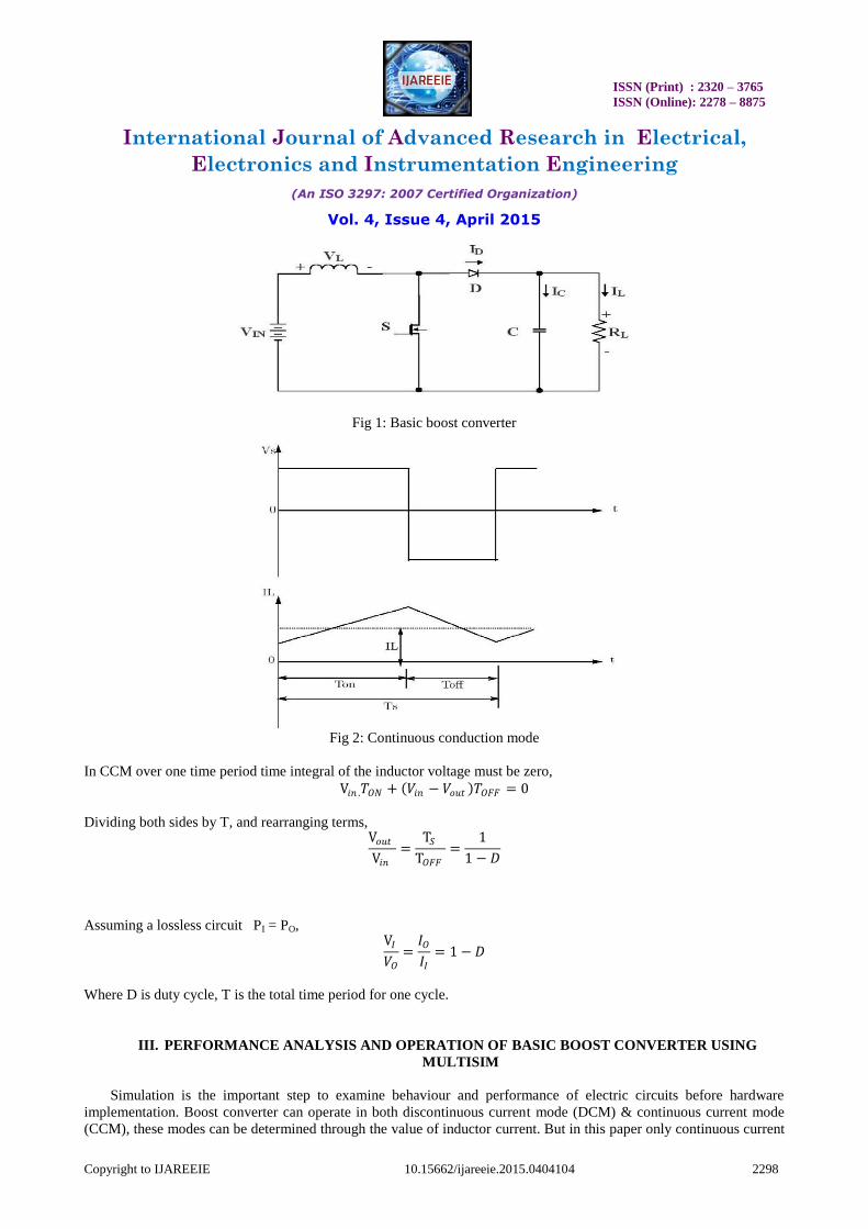
II. BASIC BOOST CONVERTER
Boost converter gives its output voltage higher than the input voltage. Operation of this converter is controlled by
periodically opening and closing an electronic switch. Fig.1 shows circuit for basic dc-dc boost-converter. This boost
converter consists of source voltage VS, inductor L, controlled semiconductor switch S (such as MOSFET/ IGBT/
BJT), diode D, capacitor C, Load Resistance RL and output voltage of converter VO. The diode D becomes OFF When
switch S gets closed and the energy from the source is gets stored into the inductor L. The diode-D becomes ON when
switch S gets opened and energy stored in the inductor gets transferred to the filter capacitor C. Longer the switch is
closed, more the energy gets stored in to the inductor and as soon as diode becomes ON this energy gets transferred to
the capacitor. Fig.2 shows square wave given to the semiconductor switch S and output current across inductor L.
For the analysis of the boost converter basic parameters used are:
I. Output voltage VO,
II. VR – Output ripple voltage,
III. IR- Output ripple current,
IV. F-the switching frequency of the switch S in Hz.
ISSN (Print) : 2320 – 3765
ISSN (Online): 2278 – 8875
International Journal of Advanced Research in Electrical,
Electronics and Instrumentation Engineering
(An ISO 3297: 2007 Certified Organization)
Vol. 4, Issue 4, April 2015
Copyright to IJAREEIE 10.15662/ijareeie.2015.0404104 2298
Fig 1: Basic boost converter
Fig 2: Continuous conduction mode
In CCM over one time period time integral of the inductor voltage must be zero,
V𝑖𝑛 .𝑇𝑂𝑁 + 𝑉𝑖𝑛 − 𝑉𝑜𝑢𝑡 𝑇𝑂𝐹𝐹 = 0
Dividing both sides by T, and rearranging terms, V𝑜𝑢𝑡
V𝑖𝑛
=T𝑆
T𝑂𝐹𝐹
=1
1 − 𝐷
Assuming a lossless circuit PI = PO, V𝐼
𝑉𝑂
=𝐼𝑂𝐼𝐼
= 1 − 𝐷
Where D is duty cycle, T is the total time period for one cycle.
III. PERFORMANCE ANALYSIS AND OPERATION OF BASIC BOOST CONVERTER USING
MULTISIM
Simulation is the important step to examine behaviour and performance of electric circuits before hardware
implementation. Boost converter can operate in both discontinuous current mode (DCM) & continuous current mode
(CCM), these modes can be determined through the value of inductor current. But in this paper only continuous current
ISSN (Print) : 2320 – 3765
ISSN (Online): 2278 – 8875
International Journal of Advanced Research in Electrical,
Electronics and Instrumentation Engineering
(An ISO 3297: 2007 Certified Organization)
Vol. 4, Issue 4, April 2015
Copyright to IJAREEIE 10.15662/ijareeie.2015.0404104 2299
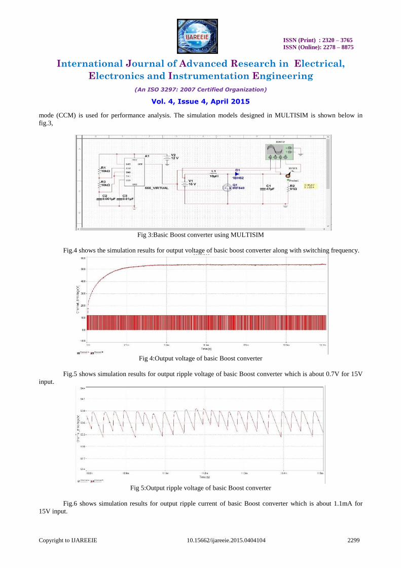
mode (CCM) is used for performance analysis. The simulation models designed in MULTISIM is shown below in
fig.3,
Fig 3:Basic Boost converter using MULTISIM
Fig.4 shows the simulation results for output voltage of basic boost converter along with switching frequency.
Fig 4:Output voltage of basic Boost converter
Fig.5 shows simulation results for output ripple voltage of basic Boost converter which is about 0.7V for 15V
input.
Fig 5:Output ripple voltage of basic Boost converter
Fig.6 shows simulation results for output ripple current of basic Boost converter which is about 1.1mA for
15V input.

ISSN (Print) : 2320 – 3765
ISSN (Online): 2278 – 8875
International Journal of Advanced Research in Electrical,
Electronics and Instrumentation Engineering
(An ISO 3297: 2007 Certified Organization)
Vol. 4, Issue 4, April 2015
Copyright to IJAREEIE 10.15662/ijareeie.2015.0404104 2300
Fig 6:Output ripple current of basic Boost converter
Following Table 1 shows variation in simulation results for output voltage ripple and output ripple current of
basic Boost converter by varying input voltage from 9V to 15V.
Input
Voltage
Input
frequency
Output
Voltage
Output
Voltage
ripple
Current
ripple
9V 35KHz 32.3V 0.3V 0.78mA
10V 35KHz 35.0V 0.4V 0.80mA
11V 35KHz 39.1V 0.5V 0.90mA
12V 35KHz 43.3V 0.5V 1.0mA
13V 35KHz 46.6V 0.6V 1.1mA
14V 35KHz 50.7V 0.7V 1.1mA
15V 35KHz 53.9V 0.7V 1.1mA
Table 1: SimulatedOutput of basic Boost converter
IV. INTERLEAVED BOOST CONVERTER
In interleaving technique an interconnection of multiple switching cells is done by synchronizing several frequency
sources which helps to increase the effective pulse frequency and operating them with phase shift related to number of
switching cells. Interleaving technique saves energy and improves power conversion without affecting conversion
efficiency. This converter is consists of two boost conversion units parallely connected, having switches S1 and S2,
inductors L1 and L2, diodes D1 and D2, Capacitor C and load resistor RL with common input source (VIN). The
Circuit diagram for interleaved dc-dc boost converter is shown in Fig.7.
The IL1-current in the inductor L1 increases linearly when the switch S1 gets turned ON, and energy gets stored in
the inductor L1. Diode D1 conducts and the stored energyin the inductor decreases with a slope based on the difference
between the input and output voltage when switch S1 is gets turned OFF. The inductor gets discharged transferring
current to load RL via diode D1. After half switching cycle of switch S1 switch S2 gets turned ON to complete the
cycle of events. Effective ripple frequency at the output capacitor is twice than that of a single-phase boost converter is
due to the combination of both the power channels at output capacitor and amplitude of the input current ripple is
small. This is the advantage of this topology for the renewable energy sources.

ISSN (Print) : 2320 – 3765
ISSN (Online): 2278 – 8875
International Journal of Advanced Research in Electrical,
Electronics and Instrumentation Engineering
(An ISO 3297: 2007 Certified Organization)
Vol. 4, Issue 4, April 2015
Copyright to IJAREEIE 10.15662/ijareeie.2015.0404104 2301
Fig 7: Interleaved Boost converter
The phase difference PD between two switching cells isgiven by,
𝑃𝐷 =360
N
Where „N‟ is the number of partially connected boost converters. Thus for a two phase interleaved boost
converter N=2 and phase difference becomes 180 degrees.
According to switching of converter it operates in three modes:
I. Mode I: switch S1 closed, switch S2 opened
II. Mode II: switch S1 opened, switch S2 opened
III. Mode III: switch S1 opened, switch S2 closed
V. PERFORMANCE ANALYSIS AND OPERATION OF INTERLEAVED BOOST CONVERTER
USING MULTISIM
The simulation models are created using MULTISIM and performance parameters of the converters are verified.
Input DC voltages are varied from 9V to 15V with constant duty cycle and output voltages are measured. The
MULTISIM simulation models for interleaved boost converteris shown below in fig.8.
Fig 8: Interleaved Boost converter using MULTISIM
Fig.9 shows the simulation results for output voltage of Interleaved Boost converter along with switching
frequency.

ISSN (Print) : 2320 – 3765
ISSN (Online): 2278 – 8875
International Journal of Advanced Research in Electrical,
Electronics and Instrumentation Engineering
(An ISO 3297: 2007 Certified Organization)
Vol. 4, Issue 4, April 2015
Copyright to IJAREEIE 10.15662/ijareeie.2015.0404104 2302
Fig 9: Output voltage of Interleaved Boost converter
Fig.10 shows simulation results for output ripple voltage of Interleaved Boost converter which is about 0.36V
for 15V input.
Fig 10: Output ripple voltage of Interleaved Boost converter
Fig.11 shows simulation results for output ripple current of Interleaved Boost converter which is about
0.70mA for 15V input.
Fig 11: Output ripple current of Interleaved Boost converter
Following Table 2 shows variation in simulation results for output voltage ripple and output ripple current of
Interleaved Boost converter by varying input voltage from 9V to 15V.

ISSN (Print) : 2320 – 3765
ISSN (Online): 2278 – 8875
International Journal of Advanced Research in Electrical,
Electronics and Instrumentation Engineering
(An ISO 3297: 2007 Certified Organization)
Vol. 4, Issue 4, April 2015
Copyright to IJAREEIE 10.15662/ijareeie.2015.0404104 2303
Input
Voltage
Input
frequency
Output
Voltage
Output
Voltage
ripple
Current
ripple
9V 35KHz 32.1V 0.20V 0.40mA
10V 35KHz 34.8V 0.23V 0.46mA
11V 35KHz 38.8V 0.24V 0.50mA
12V 35KHz 42.0V 0.27V 0.56mA
13V 35KHz 45.0V 0.31V 0.60mA
14V 35KHz 48.3V 0.33V 0.66mA
15V 35KHz 52.0V 0.36V 0.70mA
Table 2: SimulatedOutput of Interleaved Boost converter
Following Table 3 shows the comparison between conventional boost converter and interleaved boost
converter.
Parameter Boost
converter
Interleaved
Boost
converter
Input voltage 15V 15V
Switching
frequency
35K 35K
Output
voltage
53.9 V 52.0 V
Voltage ripple 0.6 V 0.36 V
Current ripple 1mA 0.7 mA
Efficiency 88% 90%
Table 3: Comparison between conventional boost converter and interleaved boost converter.
VI. CONCLUSION
This paper discusses the principle and operation of interleaved boost converter. Both the boost converters are
simulated using NI MULTISIM at fixed switching frequency and fixed duty ratio. And comparison between
conventional boostthese simulation results. These results shows the advantagesof interleaved boost converter having
higher efficiency andreduced ripple of output current by 30% and ripple of output voltage by 41%.
REFERENCES
[1] D. J. S. Newlin, R. Ramalakshmi, and S. Rajasekaran, “A performance comparison of interleaved boost converter and conventional boost
converter for renewable energy application,” in Green High Performance Computing (ICGHPC), 2013 IEEE International Conference on.
IEEE, 2013, pp. 1–6.
[2] O. Hegazy, J. Van Mierlo, and P. Lataire, “Analysis, modeling, and implementation of a multidevice interleaved dc/dc converter for fuel cell hybrid electric vehicles,” Power Electronics, IEEE Transactions on, vol. 27, no. 11, pp. 4445–4458, 2012.
[3] P. Spanik, L. Hargas, M. Hrianka, and I. Kozehuba, “Application of virtual instrumentation labview for power electronic system analysis,” in Power Electronics and Motion Control Conference, 2006. EPE-PEMC 2006. 12th International. IEEE, 2006, pp. 1699–1702.
[4] H. M. SWAMY, K. GURUSWAMY, and D. SINGH, “Design and implementation of two phase interleaved dc-dc boost converter with
digital pid controller.” [5] C.-M. Ho, H. Breuninger, S. Pettersson, G. Escobar, L. A. Serpa, and A. Coccia, “Practical design and implementation procedure of an
interleaved boost converter using sic diodes for pv applications,” Power Electronics, IEEE Transactions on, vol. 27, no. 6, pp. 2835–2845,
2012. [6] G. Reddy, D. Guna-Shekhar, S. Choudhari, and M. Ademola, “A statistical analysis package for dc-dc boost-converter design,” in Circuits
and Systems (MWSCAS), 2011 IEEE 54th International Midwest Symposium on. IEEE, 2011, pp. 1–4.
[7] F. S. Alargt and A. S. Ashur, “Analysis and simulation of interleaved boost converter for automotive applications,” in Proc. the 1st International Conference on Electrical and Computer Engineering, 2013.
[8] M. Ganta, N. Reddy, T. Akshitha, and R. Seyezhai, “Simple and efficient implementation of two-phase interleaved boost converter for
renewable energy source,” Int. J. Emerg. Technol. Adv. Eng, vol. 2, no. 4, pp. 676–681, 2012.