vk3aqz rx noise bridge kit model rx1 - vk3aqzkits.com · vk3aqz rx noise bridge kit model rx1...
TRANSCRIPT

Page | 1
VK3AQZ RX NOISE BRIDGE KIT MODEL RX1 Introduction. The VK3AQZ RX1 RF impedance bridge is designed to be built and used by students and hobbyists for the measurement of impedance in the 300 kHz to 30 MHz frequency range. The frequency of operation is from 300 kHz to 30 MHz so that readily available equipment can be used to perform the measurements. For example, a low cost AM shortwave radio can be used as the detector. This frequency range also makes it useful to radio amateurs for the measurement of transmission line characteristics, Baluns, HF antennae, small inductors, etc. The kit contains commonly available parts, or ones easily duplicated in a home workshop, in order to keep the cost low. More expensive items, such as air spaced variable capacitors, or military spec. potentiometers, could have been used but these items are expensive and difficult to source in Australia. The theoretical operation of the RF Bridge is briefly described in the following section. A more in depth coverage of the mathematics can be found in literature available on the web or in textbooks. Description and theory of operation. I have included the following AC theory in this manual to indicate that the measurement of impedance is not as simple as using a standard multimeter, and the need to recognise that it involves more complicated concepts and mathematics than simple DC theory. However that should not deter the hobbyist from building an instrument to measure it and thereby help with the practical aspects of the hobby involving radio frequency equipment and apparatus. You may wish to skip this section if you are already familiar with AC theory. Moving on, all electrical circuits consist of resistance, capacitance and inductance. We won’t dwell on the theory aspect of these properties here as this can be found in many text books. Impedance and Admittance is a combination of the 3 properties above and its value becomes important with alternating voltages and currents (AC) in a circuit. Reactance is the term used to describe the effect a capacitor or inductor has on an alternating voltage and is often described as the AC equivalent of resistance. Impedance or Admittance can be measured in terms of resistance and reactance in some series or parallel combination. So a circuit which has an impedance of a particular value can be broken down to a quantity of resistance and some quantity of reactance. The unit of measurement of impedance is the ohm and Z is the symbol. It can be expressed as a complex number or a polar number. The more usual form is the complex number where the real portion R, is the resistive component, and the imaginary portion X, is the reactive component. Written as: Z = R – jXC for a combination of resistive and capacitive reactance, and Z = R + jXL for a combination of resistive and inductive reactance.
VK3AQZKITS

Page | 2
The letter j is known as the imaginary operator and is represented by the square root of -1 which has no value, hence the term imaginary. In electrical formulae, it acts to rotate vector quantities by 90º. The equation for Z is a mathematical way of expressing impedance. You can visualise it by representing the resistance, R, as a straight horizontal line of a length which represents the size or value of R and the reactance, X, as a vertical line whose length represents the size or value of reactance and drawn at 90 degrees to the R line. The impedance, Z, is that line which goes to make up the hypotenuse of the right angle triangle so formed. Its length is the magnitude, and the angle formed with the R line, is the phase relative to the R line. By putting “j” in front of the X, it indicates to someone reading the equation that X is at 90 degrees to R. In the real world it means that the current in the capacitor or inductor (X), is not in phase with the voltage across it. For a resistor, the current in the resistor is in phase with the voltage. When you combine R and X you get some shift in phase between current and voltage. The amount of phase difference (or angle) depends on how different the sizes (magnitudes) of the R and X are relative to each other. The resulting impedance therefore has to have something in its expression that tells you how big it is (magnitude) and what it’s angle (phase) is relevant to, say, the line represented by the resistance. Hence the need to use complex numbers when describing impedance. Mathematically you can also convert a complex number to a polar number which consists of a magnitude and angle derived from the values of R and X by a relationship. If you require more information on this subject please refer to a Maths text for a more detailed explanation of complex numbers, polar numbers, and the “j” operator. Admittance is the reciprocal of impedance and consists of a conductive part (the real portion), and a susceptance (the imaginary part). The symbol for admittance is Y. The conductive part is a conductor (which can also be described as a resistor) and has a property called conductance represented by the letter G. The “susceptive” part can be an inductor or capacitor, and has a property called susceptance and is represented by the letter B. The unit of admittance, conductance, and susceptance is the siemans but was originally called “mho”. However, any combination of resistance and reactance can be expressed as either impedance or admittance by use of mathematical relationships. Such relationships can be found in many electrical textbooks. Please note that inductive reactance and capacitive susceptance are positive quantities, whilst capacitive reactance and inductive susceptance are negative quantities. This becomes important when carrying out mathematical operations on impedance and admittance measurements Impedance can be measured in a number of ways. We can either measure the individual values of resistance and reactance, or we can apply an AC signal to the combination, and by measuring the amplitude and phase of a known frequency AC signal, calculate the values. In some cases it is impractical to measure the individual values of resistance and reactance – for example the impedance of an antenna. In this case we can measure the combination. Instruments are available which can measure the signal amplitudes and phase, and from these measurements, some calculations are performed using either a microprocessor, or meter scale readings, to come up with a result. Such instruments are generally expensive but there are some hobby level kits available at reasonable prices.

Page | 3
Another method is to compare the unknown impedance to a known value of impedance. This method can be implemented using fairly simple components such as a calibrated variable resistor and calibrated variable capacitor in a simple bridge type of circuit. The bridge circuit allows the comparison to be performed by looking for a null in some applied AC signal. The RX1 uses the bridge method so as to keep the cost low and simplify the construction. The down side is that the bridge accuracy depends on the accuracy of the variable components and their calibrations. However, as an instructional tool and for amateur use, this method is low cost, easy to understand, and provides useful results. Moving on from the theory, the RX1 noise bridge consists of a wideband tone modulated noise generator feeding a variation of the Hay’s RF impedance bridge, which is the heart of the unit. The Hay’s bridge is an RF impedance version of the well known Wheatstone resistance bridge. Variations of this configuration have been duplicated and documented in radio manuals and magazines over many years. The Wheatstone bridge consists of 2 parallel strings of 2 resistors connected in series across a power supply. A meter is placed between the junctions of the 2 strings and is used as a balance detector. In figure 1, if R1 = R3 and R2 = R4, the voltage at the junctions of the 2 strings (V1 and V2) will be the same and no current will flow through the meter. It is often drawn as a diamond shaped circuit. If one of the resistors is changed in value, the voltage at the junction of the 2 resistors in the series arm will change. This will now produce a voltage difference across the meter and a current will flow. The bridge is now said to be unbalanced and a centre zero meter will show a reading. If the 2 resistors in one parallel section are replaced with a potentiometer, with the moving contact connected to one side of a centre zero meter, adjusting the potentiometer will cause the meter needle to move left or right. When the bridge is balanced the meter will read zero and the bridge is said to be “nulled”. Figure 3 shows a variation of the bridge using a balanced RF transformer in place of one parallel section. The transformer is fed from an RF signal generator. Balance is achieved when V1 = V2. Note, however, the meter is an AC meter (DC meter with diodes, or an RF probe).
FIG 1: Simple Wheatstone bridge.
FIG 2: Popular Diamond shape.
FIG 3: The bridge with transformer feed.
Page | 4
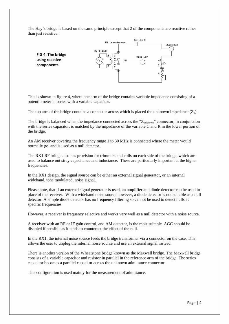
The Hay’s bridge is based on the same principle except that 2 of the components are reactive rather than just resistive. This is shown in figure 4, where one arm of the bridge contains variable impedance consisting of a potentiometer in series with a variable capacitor. The top arm of the bridge contains a connector across which is placed the unknown impedance (Zu). The bridge is balanced when the impedance connected across the “Zunknown” connector, in conjunction with the series capacitor, is matched by the impedance of the variable C and R in the lower portion of the bridge. An AM receiver covering the frequency range 1 to 30 MHz is connected where the meter would normally go, and is used as a null detector. The RX1 RF bridge also has provision for trimmers and coils on each side of the bridge, which are used to balance out stray capacitance and inductance. These are particularly important at the higher frequencies. In the RX1 design, the signal source can be either an external signal generator, or an internal wideband, tone modulated, noise signal. Please note, that if an external signal generator is used, an amplifier and diode detector can be used in place of the receiver. With a wideband noise source however, a diode detector is not suitable as a null detector. A simple diode detector has no frequency filtering so cannot be used to detect nulls at specific frequencies. However, a receiver is frequency selective and works very well as a null detector with a noise source. A receiver with an RF or IF gain control, and AM detector, is the most suitable. AGC should be disabled if possible as it tends to counteract the effect of the null. In the RX1, the internal noise source feeds the bridge transformer via a connector on the case. This allows the user to unplug the internal noise source and use an external signal instead. There is another version of the Wheatstone bridge known as the Maxwell bridge. The Maxwell bridge consists of a variable capacitor and resistor in parallel in the reference arm of the bridge. The series capacitor becomes a parallel capacitor across the unknown admittance connector. This configuration is used mainly for the measurement of admittance.
FIG 4: The bridge using reactive components

Page | 5
The RX1 bridge is configured as an impedance bridge but it can also be wired as an admittance bridge by altering a couple of connections, and moving the series C so as to become a parallel C. However, most measurements made by radio amateurs and hobbyists will be impedance. Referring back to figure 4, the series C allows the bridge to be used for both negative reactance (capacitive) and positive reactance (inductance). If you place a short circuit across the Zunknown connector, the bridge will be balanced when the variable resistor (R control) is zero, and the variable capacitor (RX control) has a value equal to the series capacitor. In the RX1 bridge, the value of the series capacitor is 120 pf, which places the zero reactance null at approximately half travel of the capacitor. In the kit, it actually consists of a trimmer capacitor in parallel with a fixed capacitor. The trimmer allows the user to set the zero reactance on the zero dial marking. The dial calibrations are for a value of 120 pf series capacitor. The reactance spreadsheet supplied with the RX1 uses this value in the formulae. In the RX1 bridge, the RX dial marked “+C” represents the value of capacitance placed across the Zu terminal and ranges from 20 pf at one end of the dial, to infinity at the zero null mark in the centre of the dial. Dial markings for values from around 1000 pf to infinity, are very close and not really usable. A chart or spreadsheet is used to find the value of reactance at the test frequency. The dial section marked “-C” represents the value of capacitance placed in parallel with the internal series C, and ranges from around 2 pf to just under 100pf. A chart or spreadsheet is used to find the equivalent inductive reactance, and inductance values, at the test frequency. The reason an inductive reactance can be measured in this way may at first seem strange. However, placing an inductor across the unknown connector will cancel some of the series capacitance. The variable capacitor will then find a zero reactance null at a different setting, or value. The exact values are a little more complex to calculate but essentially, the bridge will be nulled when the reactance of the variable capacitor (Xvc), is equal to the reactance of the internal 120 pf series capacitor (Xcs) minus the reactance of the inductor (XL). The RX1 kit contains spreadsheets and charts to allow you to find the values of reactance at specific frequencies for +C and –C dial readings. The inductive portion of the reactance dial is marked “-C” in line with several other designs published over the years.
FIG 5: The admittance version of the bridge
Page | 6
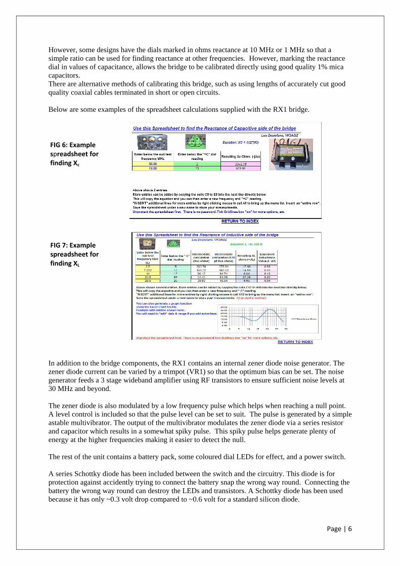
However, some designs have the dials marked in ohms reactance at 10 MHz or 1 MHz so that a simple ratio can be used for finding reactance at other frequencies. However, marking the reactance dial in values of capacitance, allows the bridge to be calibrated directly using good quality 1% mica capacitors. There are alternative methods of calibrating this bridge, such as using lengths of accurately cut good quality coaxial cables terminated in short or open circuits. Below are some examples of the spreadsheet calculations supplied with the RX1 bridge. In addition to the bridge components, the RX1 contains an internal zener diode noise generator. The zener diode current can be varied by a trimpot (VR1) so that the optimum bias can be set. The noise generator feeds a 3 stage wideband amplifier using RF transistors to ensure sufficient noise levels at 30 MHz and beyond. The zener diode is also modulated by a low frequency pulse which helps when reaching a null point. A level control is included so that the pulse level can be set to suit. The pulse is generated by a simple astable multivibrator. The output of the multivibrator modulates the zener diode via a series resistor and capacitor which results in a somewhat spiky pulse. This spiky pulse helps generate plenty of energy at the higher frequencies making it easier to detect the null. The rest of the unit contains a battery pack, some coloured dial LEDs for effect, and a power switch. A series Schottky diode has been included between the switch and the circuitry. This diode is for protection against accidently trying to connect the battery snap the wrong way round. Connecting the battery the wrong way round can destroy the LEDs and transistors. A Schottky diode has been used because it has only ~0.3 volt drop compared to ~0.6 volt for a standard silicon diode.
FIG 6: Example spreadsheet for finding Xc
FIG 7: Example spreadsheet for finding XL

Page | 7
The battery pack is 9 volts and uses 6 low cost AA batteries. However, a 9 volt standard battery can also be used. With the LEDs turned on, the current drawn is around 30 mA. If the LEDs are omitted, the current drain falls to around 8 mA. The design of the wideband amp is such as to keep the current drain to a minimum. We will now describe the assembly and calibration of the RX1 kit. Because this kit was designed for technology students and hobbyists, it contains standard electronic components and mechanical parts which can be produced in a modestly equipped workshop. This allows the student to become familiar with some basic construction techniques and hopefully illustrate that it is possible to construct an electronic device that is of an acceptable standard in a small laboratory or workshop. Kit contents. Before starting to assemble the kit, check that all the components have been supplied. Refer to the “Component list” for details. Assuming all the components are there, and correct, you can commence the assembly process. You will need the following tools: Soldering iron with fine and large tips, a pair of fine tipped side cutters, small and medium sets of pliers, a set of cross head and flat blade screwdrivers of various sizes, a 2mm or 5/64th” Hex key for the knob grub screws, a 3mm nut driver and a pair of tweezers would be useful, a multimeter, an alignment tool set with a small flat blade for trimmers and trimpots, clip leads and small file. A receiver with AM covering the range 1 to 30 MHz is required. Other test equipment, such as an oscilloscope and frequency counter, will help but are not essential. A 12v PC fan running from a battery or plug pack maybe suitable if the soldering rate is low enough.

Page | 8
Tools
Test equipment
Receiver –which one is yours?
Optional
Hex key size needed for knob grub screws
4mm drill or rod for winding the compensation coil
Rhonda‘s first radio (my xyl, vk3zyl)
Hallicrafters SX17 Collins 51j4 Hallicrafters SX112
My Sangean ATS803a Grandfather’s
Page | 9
Assembly. Suggested assembly steps:
1. Mount noise and tone generator components onto noise generator board. 2. Test noise generator board. 3. Mount base PCB into case 4. Mount rear panel connectors to rear panel PCB and attach to case. 5. Solder rear panel PCB to base PCB in 3 spots. 6. Construct RF transformer and mount onto RF deck PCB. 7. Mount RF deck to rear panel and base using 25mm spacers. 8. Mount RF deck components and wire to J3, J4 and J5. 9. Mount tuning capacitor, potentiometer, LEDS, etc. to control PCB. 10. Attach aluminium bracket to control PCB and mount bracket with PCB to base. 11. Solder short wire between top terminal of potentiometer to 3F pad on RF deck. 12. Mount power switch to small power PCB, attach power leads and fix to case. 13. Attach power lead to control PCB LED terminal strip, check for shorts, and power up to test
LEDS. 14. Attach tuning capacitor coupler to tuning capacitor shaft. 15. Attach potentiometer brass coupler to potentiometer shaft. 16. Attach dial scales to drums and fit into case with supplied plastic and brass shafts. 17. Attach knobs. 18. Check alignment of shafts. Adjust/expand holes/etc to obtain straight alignment. 19. Prepare the short shielded cable and fit to terminal block on noise board. 20. Attach fig 8 power cable to noise board and fit board to case. 21. Solder shielded cable to rear of J2, nearest RCA socket. 22. Make short shielded cable loop using RCA plugs and fit to rear RCA sockets. 23. Attach cursor and label to lid then D handles. 24. Fit battery shield. 25. Test for short circuits on power lines then fit AA batteries and proceed to testing.
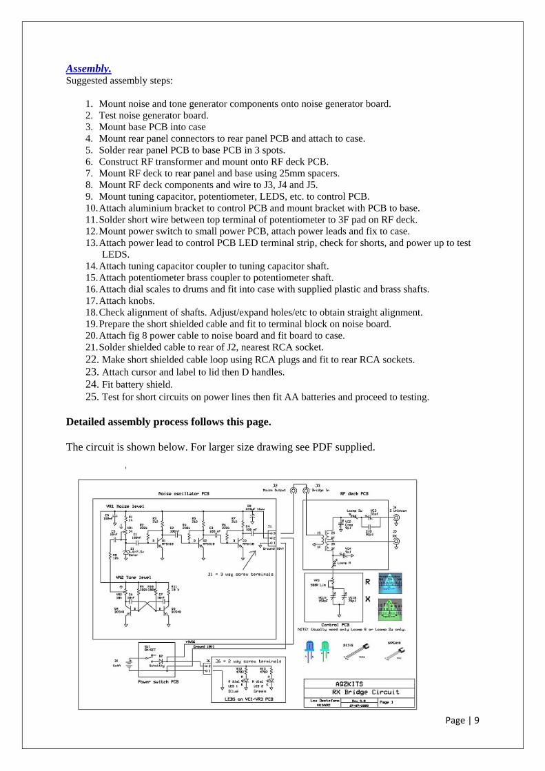
Detailed assembly process follows this page. The circuit is shown below. For larger size drawing see PDF supplied.
Page | 10
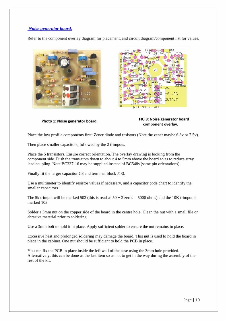
Noise generator board. Refer to the component overlay diagram for placement, and circuit diagram/component list for values. Place the low profile components first: Zener diode and resistors (Note the zener maybe 6.8v or 7.5v). Then place smaller capacitors, followed by the 2 trimpots. Place the 5 transistors. Ensure correct orientation. The overlay drawing is looking from the component side. Push the transistors down to about 4 to 5mm above the board so as to reduce stray lead coupling. Note BC337-16 may be supplied instead of BC548s (same pin orientations). Finally fit the larger capacitor C8 and terminal block J1/3. Use a multimeter to identify resistor values if necessary, and a capacitor code chart to identify the smaller capacitors. The 5k trimpot will be marked 502 (this is read as 50 + 2 zeros = 5000 ohms) and the 10K trimpot is marked 103. Solder a 3mm nut on the copper side of the board in the centre hole. Clean the nut with a small file or abrasive material prior to soldering. Use a 3mm bolt to hold it in place. Apply sufficient solder to ensure the nut remains in place. Excessive heat and prolonged soldering may damage the board. This nut is used to hold the board in place in the cabinet. One nut should be sufficient to hold the PCB in place. You can fix the PCB in place inside the left wall of the case using the 3mm hole provided. Alternatively, this can be done as the last item so as not to get in the way during the assembly of the rest of the kit.
FIG 8: Noise generator board component overlay.
Photo 1: Noise generator board.

Page | 11
Rear connector panel and base board assembly The rear connector panel is a single sided PCB material which is placed inside the case at the rear, and has 4 connectors on it. The connectors are screwed to the panel on the non copper side such that the connector flanges are between the panel and the plastic case. 3 of the connector screw holes are also used to attach the panel to the case. A 4mm nut is used as a spacer on these 3 screws so that the panel clears the internal ribs. The copper side of this panel faces the inside of the case and will have the RF deck PCB soldered to it at a later stage. There is also a single sided piece of PCB used as the base. This lays flat on the bottom with the copper side up and goes hard up against the rear of the case. The rear connector panel sits on top of this base and the two are electrically connected at the bottom junction with 3 solder joints. The base plate has 4 holes in it which line up with 4 countersunk screw holes in the bottom of the case. The 2 holes closer to the rear are used for a pair of pillars connected to the RF deck. The remaining 2 holes are used to attach an aluminium bracket which supports the controls on the control PCB. This will be detailed in a later section. First step is to place the bottom PCB in place. Temporarily use 3mm x 10mm countersunk cross head screws with 3mm nuts to hold it in place. With the copper surface facing upwards, the board holes should line up correctly with the case holes. Now attach the 2off SO239 sockets to the rear panel PCB with the flanges on the non copper side. Attach the RCA phono socket panel also. One edge has been cut back to fit in the space available. The uncut edge goes up against the closest SO239 flange (J5 – Receiver). At this stage, attach the SO239 sockets with only 3 bolts. Use 3mm x 10mm long cross dome head bolts with star washers. For a good electrical connection, lightly tin around the 4 screw hole areas of the PCB for SO239 connectors. Do not put a bolt in the top left hole on J4 (Z unknown) and the top right bolt on J5 (Receiver socket). (looking from the rear). Similarly, leave out the far right bolt for the RCA phono sockets panel. The reason for this is that these 3 holes will be used to hold the rear panel PCB to the case using longer bolts and spacers. You can now attach the panel to the rear. This is attached with 3mm x 16mm long cross head dome bolts through the above mentioned holes. Poke 3 bolts through the 3 small holes in the rear of the case. Place a 4mm nut on each bolt to act as a spacer. Then carefully bring the rear panel with connectors on it, up against the rear so that the 3 bolts pass through the holes on the connector panels which were left unfilled. Take care not to knock the spacers off the bolts. Use 3mm nuts and star washers to complete the attachment. The holes in the rear PCB are slightly larger than 3mm to allow for small tolerance variations. Before soldering the base PCB to the rear PCB, just visually check that it is square with the rear panel. Now place 3 solder joins at the junction of the base PCB and the bottom of the rear panel. Place one in the centre and one at each end. There is no need to overfill the join as long as the fills are solid and clean. Making more than 3 joins will make it difficult to separate the panels should there be a need to service or replace them for any reason. That completes this section of the assembly.

Page | 12
RF deck assembly. The RF deck consists of a PCB which contains most of the RF bridge components. It consists of a single sided fibreglass PCB soldered to the rear connector panel. The RF transformer, compensation trimmers and coils, and series capacitor are mounted on the RF deck PCB on the copper pads side facing upwards. 2off 25mm spacers are used to support the RF deck prior to soldering it to the rear panel. Most of the components are soldered on the pads after the PCB is attached to the rear panel. This makes it easier to solder this PCB to the rear panel without having the trimmers and other components in the way. The trimmer capacitors are made of plastic and can be damaged if accidently touched in the wrong spot by the soldering iron tip during the mounting of the PCB. Remove the temporary nuts on the bottom PCB, which are on the bolts closest to the rear panel. Using the same countersunk bolts, screw them into one end of the tapped 25mm pillars supplied. These pillars are needed to hold the RF deck in place prior to soldering it to the rear panel. They also stop the RF deck bending down when adjusting the trimmers. However they don’t need to be structurally strong or over tight. Before you mount the RF deck in place, you can place the RF transformer in place first. This makes it a little easier to manipulate the zip tie around the transformer. So we will now jump to the construction details of the RF transformer. The RF transformer consists of a 3 turn primary winding and a 3 turn secondary winding. The primary winding is a single length of 0.3mm enamelled copper wire 140mm long. The secondary winding consists of 2 lengths, 140mm long, of the same wire twisted together to form a bifilar pair. The bifilar winding is made by twisting them together with about 6 twists per 25mm (1”). This can be done neatly by placing one end of the pair of wires in a small drill chuck and the other end in a small vice. Slowly turning the chuck should result in a neat even twist. Use a ruler to confirm the 6 twists per inch. Once the lengths of wire have been prepared, you can thread them through the 2 hole balun core supplied. The balun core is a 43 grade Ferrite material designed to work over the range 1 to 30 MHz. First wind the secondary by passing 3 turns of the bifilar pair through the core. 1 turn is equal to passing the wire through both holes in the core once. The ends will be on the same side of the core.
Photo 2: Preparing the transformer windings.

Page | 13
The primary winding consists of 3 turns through the core but starting at the opposite end of the core. Once completed, you should have one pair of wires at one end of the core representing the primary winding, and 2 sets of wires at the opposite end, representing the balanced dual secondary. The ends can now be tinned. The enamel coating will burn off when the iron is applied to the tip. Use a fan to blow the fumes away. They can be trimmed later if necessary. The leads are identified as per the drawing. The start of the primary winding is labelled 1S and the finish is labelled 1F. In a similar manner, the 2 secondary’s are labelled 2S, 3S and 2F, 3F. Take careful note of which wires are the start and finish of each winding. The centre tap of the secondary is wire 2F connected to 3S. If you join the wrong ends, the bridge will not work correctly. You can use a multimeter to confirm you have the 2 secondaries in series. If winding 2 and 3 are not connected in series, then they will effectively be shorted out (i.e. 2S connected to 2F and 3S connected to 3F!!). The accuracy of the bridge will depend on how symmetrical and neat the transformer is constructed. Before joining the wires to form the secondary centre tap, ensure the 3 wires are not shorting to each other (due to nicks or cracked enamel) by using a multimeter. A short in one of the windings will produce a bridge which will not balance correctly. The transformer can now be zip tied onto the board. Refer to the photo of this board for correct placement. Now place the RF deck in place by using a couple of 3mm x 10mm cross head bolts into the top of the pillars using the end holes on the RF deck PCB. The PCB should sit up against the rear panel with the small recesses aligning with the SO239 protrusion. It should sit just below the SO239 centre spigots. You can now solder the RF deck PCB to the back panel in 3 places on the panel. These are at each end and near the centre SO239 socket. Push the PCB against the back panel when soldering the 2 pieces together. You can now place the components on the board. Start by soldering the small 82 pf capacitor (C10) in the location shown in the photo.
Photo 3: Completed transformer.
Photo 4: Location of C10, 82pf capacitor

Page | 14
Bend the leads outwards so that the capacitor sits over the pads. Be careful not to damage the ceramic casing. Leave one pigtail uncut. This will be connected to J4 centre spigot as a bridge between the spigot and the pad underneath. Please note that this capacitor is a Philips 600 series NPO ceramic capacitor with low loss, low inductance, and good stability. To ensure bridge stability and performance, do not substitute a lower grade capacitor for C10. Solder trimmer capacitor VC3 in parallel with the 82pf capacitor. This is a 57pf max trimmer and is the larger of the trimmers in the kit. It is a good quality low loss unit made by Philips and used in VHF/UHF transmitting equipment. However it is easily damaged by excessive heat from the soldering process. Ensure the joint is done quickly and cleanly on the legs. Bend the legs carefully outwards so they sit on the pads. Do not substitute a low quality trimmer as it will affect the bridge performance and stability. A good quality ceramic or air trimmer would also suit. At this stage, if you prefer, the RF transformer leads can now be soldered in place. One lead of the primary (1S) goes to the centre spigot of the closer RCA socket (J3). There is a pad on the PCB you can also use if you wish. If you use the pad, then use a short piece of wire from the pad to the RCA centre pin. The centre pin of the RCA socket is sensitive to heat. In order to ensure you don’t distort the location of the pin, you need to solder as quickly as possible. If you plug an RCA plug into the socket prior to soldering, the pin on the plug will help keep the socket spigot in place. This is well worth doing and gives you more time to solder the wire. The same applies to the SO239 sockets. The SO239 sockets use a white heat sensitive material which can distort if overheated. Again, a dummy plug plugged into the socket while soldering to the spigot, will reduce the damage. The other side of the primary (1F) goes to the PCB earth just near the RCA socket earth pin. Now solder the secondary wires in place. The centre tap, consisting of 2F and 3S twisted together, can be soldered to the centre spigot of the RX SO239 socket (J5). Wire 2S goes to a nearby pad. This pad has one end of a small compensation coil (Lcomp Zu) attached to it, and the middle leg of VC2, a small 2 – 9 pf plastic trimmer, on it. The other 2 legs of VC2 sit on an earth pad soldered to the rear panel nearby.
Photo 5: Location RF transformer
Photo 6: RF deck with transformer
d

Page | 15
The other end of the compensation coil goes to the pad with the centre wire of VC3 on it. VC3 is the 57 pf trimmer in parallel with the 82 pf ceramic capacitor. The compensation coil starts off as 4 turns wound on a 4mm diameter drill spread over 5 to 10mm. However during the tune up stage, this coil may end up smaller or larger depending on the amount of compensation required. Refer to the photos for details. In one case it was reduced to a single turn. The end SO239, J4 (Z unknown) has the centre spigot soldered to the nearby pad with the other end of C10 and VC3 on it. You can use the pigtail on C10 bent upwards to bridge the connection. Place a dummy PL259 plug in the socket to reduce heat damage. The remaining secondary wire (3F) goes to a small pad which also has a small 2 – 9pf trimmer (VC4) on it, and also a possible compensation coil (Lcomp R). However, you probably will not need this coil. The pad has been provided in case the bridge requires inductive compensation on the variable R/C side of the bridge. However, this side of the bridge has a significant amount of inductance due to the wire going to the potentiometer and variable capacitor. To compensate for this inductance, the coil going to the Z unknown connector will most likely be required to balance the bridge. Please note that VC2 and VC4 are also required to compensate for stray capacitance on each side of the bridge and around the various components, including the transformer windings. In theory only VC2 should be needed, which compensates for stray capacitance associated with the potentiometer. However, it has been found that both VC2 and VC4 are needed to reduce other strays in the bridge. The setting of these 2 trimmers tends to cancel each other to some degree but in practice they both need to be adjusted for best performance. This will be detailed later. Please note that the potentiometer casing is not connected to earth in order to reduce stray capacitance. This completes the installation of the RF deck.
Photo 8: Compensation coil construction
Photo 7: Lcomp Zu location.
Page | 16
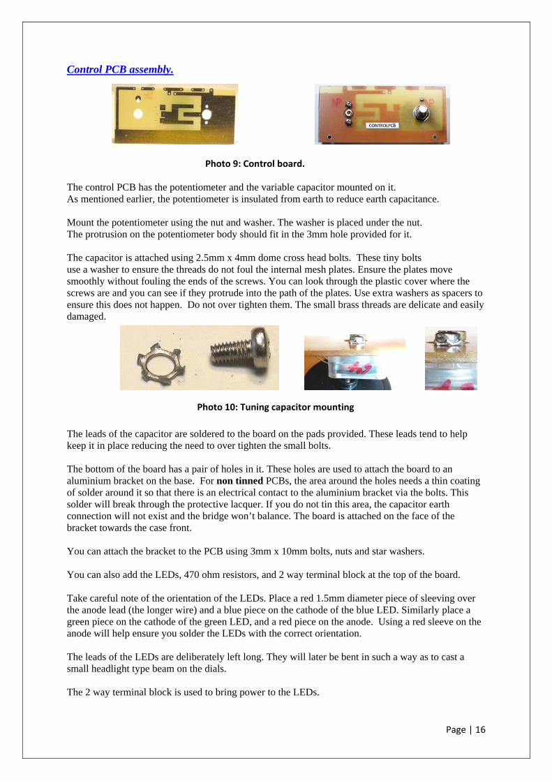
Control PCB assembly. The control PCB has the potentiometer and the variable capacitor mounted on it. As mentioned earlier, the potentiometer is insulated from earth to reduce earth capacitance. Mount the potentiometer using the nut and washer. The washer is placed under the nut. The protrusion on the potentiometer body should fit in the 3mm hole provided for it. The capacitor is attached using 2.5mm x 4mm dome cross head bolts. These tiny bolts use a washer to ensure the threads do not foul the internal mesh plates. Ensure the plates move smoothly without fouling the ends of the screws. You can look through the plastic cover where the screws are and you can see if they protrude into the path of the plates. Use extra washers as spacers to ensure this does not happen. Do not over tighten them. The small brass threads are delicate and easily damaged. The leads of the capacitor are soldered to the board on the pads provided. These leads tend to help keep it in place reducing the need to over tighten the small bolts. The bottom of the board has a pair of holes in it. These holes are used to attach the board to an aluminium bracket on the base. For non tinned PCBs, the area around the holes needs a thin coating of solder around it so that there is an electrical contact to the aluminium bracket via the bolts. This solder will break through the protective lacquer. If you do not tin this area, the capacitor earth connection will not exist and the bridge won’t balance. The board is attached on the face of the bracket towards the case front. You can attach the bracket to the PCB using 3mm x 10mm bolts, nuts and star washers. You can also add the LEDs, 470 ohm resistors, and 2 way terminal block at the top of the board. Take careful note of the orientation of the LEDs. Place a red 1.5mm diameter piece of sleeving over the anode lead (the longer wire) and a blue piece on the cathode of the blue LED. Similarly place a green piece on the cathode of the green LED, and a red piece on the anode. Using a red sleeve on the anode will help ensure you solder the LEDs with the correct orientation. The leads of the LEDs are deliberately left long. They will later be bent in such a way as to cast a small headlight type beam on the dials. The 2 way terminal block is used to bring power to the LEDs.
Photo 9: Control board.
Photo 10: Tuning capacitor mounting

Page | 17
Once the board has its components and base bracket fitted, you can attach it to the bottom PCB. Use the countersunk 3mm bolts and nuts to hold it in place. Again, a very thin layer of solder tinning should be placed around the holes on the base PCB so as to break through the lacquer. The shaft of the pot and the centre of the tuning capacitor should line up exactly with the 2 holes in the front panel of the case. If not, the shafts will be at an angle and not turn correctly. The holes in the aluminium bracket are 4mm, and this allows the bracket and control PCB to be moved so that the PCB is square with the front panel. The shafts should be straight. Loosen the nuts on the bracket slightly so you can adjust its position. Once it looks correct you can tighten them up with a nut driver. If they still don’t line up (due to tolerance errors) increase the size, or slot the holes till everything lines up correctly. The shafts should be a nice smooth fit in the front panel holes so as to act as a form of bearing for the shafts. The location of this PCB has been carefully designed so that the dial wheels are close enough to the lid cursor and dial windows. Once you commence assembly of the dials, this will start to become apparent. You can now attach the variable capacitor shaft coupler. This is attached to the small black plastic disc that is supplied with these capacitors using a couple of 3mm x 10mm cross head dome bolts through the 2 holes in the black plastic disc. The nuts go on the copper coupler side. The small centre screw should be left in place when attaching the coupler. The black disc and coupler are assembled before the black disc is attached to the variable capacitor. The centre of the coupler is a 7mm brass tube. A small crosshead screw driver is inserted in the centre of the tube and used to turn the 2.5mm tiny bolt in the centre so as to attach it to the variable capacitor. Don’t over tighten this screw. It should be just firm enough to ensure the assembly is attached to the variable capacitor. Use a long thin screwdriver through the hole in the front of the case. The screwdriver blade should line up with the coupler tube and enable you to turn and tighten the small 2.5mm screw inside the coupler to the capacitor shaft. Once attached, turn the coupler and ensure it is centered correctly. If not, some small adjustment is possible by loosening the 2 small bolts and aligning the coupler to the plastic disk by looking down the centre of the brass tube. You can now proceed with the installation of the dials and shaft couplers.
Photo 11: Variable capacitor coupler. Insert shaft into coupler after passing through case and drum.
Page | 18
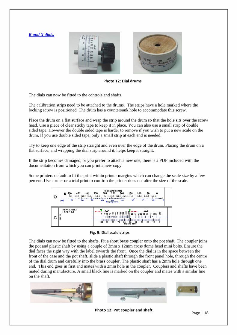
R and X dials. The dials can now be fitted to the controls and shafts. The calibration strips need to be attached to the drums. The strips have a hole marked where the locking screw is positioned. The drum has a countersunk hole to accommodate this screw. Place the drum on a flat surface and wrap the strip around the drum so that the hole sits over the screw head. Use a piece of clear sticky tape to keep it in place. You can also use a small strip of double sided tape. However the double sided tape is harder to remove if you wish to put a new scale on the drum. If you use double sided tape, only a small strip at each end is needed. Try to keep one edge of the strip straight and even over the edge of the drum. Placing the drum on a flat surface, and wrapping the dial strip around it, helps keep it straight. If the strip becomes damaged, or you prefer to attach a new one, there is a PDF included with the documentation from which you can print a new copy. Some printers default to fit the print within printer margins which can change the scale size by a few percent. Use a ruler or a trial print to confirm the printer does not alter the size of the scale. The dials can now be fitted to the shafts. Fit a short brass coupler onto the pot shaft. The coupler joins the pot and plastic shaft by using a couple of 2mm x 12mm cross dome head mini bolts. Ensure the dial faces the right way with the label towards the front. Once the dial is in the space between the front of the case and the pot shaft, slide a plastic shaft through the front panel hole, through the centre of the dial drum and carefully into the brass coupler. The plastic shaft has a 2mm hole through one end. This end goes in first and mates with a 2mm hole in the coupler. Couplers and shafts have been mated during manufacture. A small black line is marked on the coupler and mates with a similar line on the shaft.
Fig. 9: Dial scale strips
Photo 12: Dial drums
Photo 12: Pot coupler and shaft.

Page | 19
It may be slightly tight but be careful not to over exert the shaft to avoid damage to the pot. Line up the 2mm holes in both ends of the coupler and use 2mm x 12mm cross dome head mini bolts, with star washer, to join the items. Fit the small bolt on the dial side first followed by the bolt to the pot second. The dial uses a long wood screw to lock it in place. Ensure this is not tight when pushing the shaft through the centre of the dial. This screw will be tightened up later when the scale is lined up with the cursor on the lid. There should be a small clearance of around 1 or 2 mm between the dial and the ribs inside the case front allowing the drum to rotate freely. Once the shafts are fitted, you can fit the silver black knobs. You will need a 2mm or 5/64” hex key for the grub screws. The leads on the LEDs will need to be bent so that the front of the LEDs just sit near the edge of the dial drum. A small kink in the leads will be needed in order that the headlight beam falls neatly on the scale. A bit of manipulation will be needed to get this right. This can be done when the power is wired to the 2 way terminal block on the control board. A short piece of wire is used to connect the top terminal of the pot to the RF deck pad which goes to 3F. For now, that completes the installation of the RF deck and control PCB. The power wires can be added later. Power switch PCB. The power on/off switch is fitted to the front of the case in the 6mm hole provided. Remove the back nut so as to leave sufficient thread to attach the front nut with washers. The small, 3 strip PCB, is placed on the switch mounting thread with the copper strips facing into the case. These strips act as anchor points for the battery snap wires and switched DC leads going to the noise generator and the control PCB 2 way terminal block for the LEDs. The battery snap black wire goes to the middle strip and the red wire to the left strip towards the side. A short PVC covered wire goes from this strip to the middle terminal of the switch. The top switch terminal goes to the remaining strip on the other side via the Schottky diode D2. Using the PCB is much easier than trying to fit several wires onto the switch terminals. Be careful not to overheat the switch terminals. The materials used in these switches are somewhat heat sensitive also. You can fit the switch to the panel and case first, and then solder the wire leads. Or you can just attach the PCB to the switch shaft, and attach the wires first. Then attach the PCB with switch and wires, to the panel.
Photo 13: Power switch and PCB
SPDT or SPST
Page | 20
Completing the internal wiring 2 lengths of fig 8 cable are attached to the switch PCB. One length, about 200mm long, will go to the control board with the LEDs on it, and the other, about 400mm long, will go to the noise generator. The red wires go to the strip with the diode on it (switched 9 volts), and the black stripe wires to the middle strip (zero volts or earth). Use any convenient spot on the strips. Twist the 2 reds together first so that only one joint is required. Similarly for the black stripe wires. A piece of blank PCB is used to separate the battery from the rest of the unit. This PCB has corners cut away to allow the leads to pass from the battery compartment into the rest of the case. Use whichever cutaway is easier. Using the front cutaway reduces the fig. 8 cable lengths. The fig 8 lead going to the noise board is passed under the RF deck, and emerges near the 3 way terminal block on the noise board. There should be enough cable to allow you to lift the noise board up and insert the leads into the terminal block. This block will also have the shielded noise output cable connected to it. The braid of the noise cable goes to terminal hole 1 along with the black wire in the fig 8 lead. The centre wire of the noise cable goes into hole 3 and takes the noise signal to J2, the rear panel RCA phono socket nearest to the side. The braid of this cable is soldered to the earth near J2. When making this short lead, place some heat shrink tubing over the braid and cable end for neatness. You can use some of the small pieces included in the kit. The red wire of the fig 8 cable goes into hole 2 (the middle) and supplies 9v to the board. The fig 8 lead going to the LEDs on the control board passes under the pot shaft and into the 2 way block near the top. This block is designed to have the wires fitted sideways with the screw terminals accessible from the top. The red wire goes to hole 2, which is on the right hand side looking from the front, and feeds the 2 resistors going to the LEDs. The black stripe wire goes to hole 1, and is the earth return. When inserting the bare ends of the wires into the terminal holes, make sure they enter correctly. It is possible to push the wires in but miss the screw clamp. The noise generator board can now be fitted into the case using a 3mm x 16mm bolt through the hole in the left side of the case and into the nut soldered onto the bottom of the board. Some short Zip ties have been included to help tidy up the wiring. That completes the internal assembly and wiring.
Photo 13: Noise output cable end.

Page | 21
Fitting the lid and cursors. The lid can now be prepared and fitted. The lid has 2 circular cut outs which sit over the dials. The cursors consist of plastic film with a fine black line through the centre area where the 2 dials are. This plastic film is attached using a few pieces of 12mm wide double sided tape. Align the cursor line with the centre of the holes. Later during calibration, the drums can be rotated and locked using the locking wood screws so as to align correctly with the cursors. This will allow small deviations of the line from the centre of the holes. However, try to make any deviation as small as possible so that the cursor looks centred and straight in the hole. Once the cursors are fixed in place, attach the 2 satin chrome D handles, using the 4mm cross head dome bolts and star washers provided. You can now attach the front panel laminated label using some strips of 12mm wide double sided tape provided. Centre the label between the handles and with the designations opposite the various connectors, etc. A copy of this label has been included in a PDF so that more can be printed and laminated if required. Maybe you would prefer an alternative colour and designations. It is not difficult to produce a label in this manner. Having completed the assembly, you can now proceed with the testing and calibration.

Page | 22
TESTING AND CALIBRATION OF THE BRIDGE Fit 6 off new AA batteries in the battery holder and using a multimeter check you have around 9 volts DC at the battery holder snap terminals. Connect the battery snap and operating the front panel switch should bring on the 2 LEDs on the control PCB. If not, check for shorts, incorrect wiring, LEDSs connected correctly, etc. Use a multimeter to trace the wiring and voltages. If the LEDs light up, you can proceed with the testing of the noise board. Suggested testing and calibration steps:
1. Test the noise board. Check voltages and listen on a receiver for noise and tone. 2. Adjust dial drums on shafts so that end of scale logging marks (0 and 100) line up with end of
travel for both potentiometer and tuning capacitor. 3. Attach receiver and solder a short circuit across the back of the Z unknown connector. 4. Turn on bridge, LEDS should light, and turn R dial to zero and X dial should null somewhere
near centre. 5. Set small trimmers to minimum. 6. Place set zero mark on X dial under cursor and adjust VC3, large trimmer, for null at 1MHz. 7. Tune receiver to 28MHz and adjust Lcomp Zu for a null at the set zero mark. Stretch or trim
coil till null occurs at set zero mark for both 1MHz and 28MHz. 8. Remove the short circuit from Zu and solder a small 430 (or 432) ohm resistor from centre
spigot to earth. 9. Set X dial to zero and R dial to 430 (or 432) ohms. 10. Adjust VC4 and VC2 for a null at 1MHz. Try VC2 first. IF there is no null return VC2 to
minimum and adjust use VC4. Do not adjust R dial during this. Rock X dial for a deeper null. 11. Tune receiver to 28MHz and find a null on the X dial. Do not adjust R dial. 12. Carefully adjust VC4 for a null at the zero point on the X dial. Check the null on the R dial. 13. Repeat these steps till the null occurs at 430 ohm (or 432) on the R dial and zero on the X dial
at 1MHz and 28MHz. 14. Check that the low end limit of the X dial is 20pf using the supplied 2x10pf ceramic
capacitors soldered across the Zunknown connector. Adjust trimmer on rear of tuning capacitor for a null at the set 20pf mark. Small variations don’t require adjustment.
15. Replace the short circuit and make any slight corrections to the set zero mark on the X dial at 1MHz using VC3 and 28MHz by adjusting the compensation coil.
16. Recheck the 430/432 ohm calibration. 17. Remove the short circuit and solder a 49.9 ohm resistor across Zu. Should read 50 ohms plus
or minus a small amount. Rotate drum if you require it exactly under cursor. The 430/432 ohm setting will shift slightly but can be corrected also by repeating the previous steps if desired.
18. Adjust LEDS for the desired headlight beam on the dials and complete the construction by fitting the lid screws and rubber cups in place.
More detailed steps follow.

Page | 23
Testing noise generator board. Note: The noise board can be checked immediately after you complete mounting the parts. In this case use the battery snap and the protective Schottky diode in series to power the board up outside the case. The following instructions apply whichever way you decide to proceed. Check you have around 9 volts DC on the terminal block. Check the zener diode voltage. A multimeter across D1 should read around 6.8 v ± 0.5v (or 7.5v ± 0.5v if 7.5 v zener supplied) with noise level trimpot at half way. Check the base bias on RF transistors Q1, 2, and 3. Prior to testing the bias, the noise and tone levels should be reduced to a very low level. The presence of noise and tone will affect the bias readings – particularly the second transistor. A meter on the collectors of Q1, Q2 and Q3 should read around half supply voltage = 4 to 6 volts. This may even be from 3 to 7 volts which is okay but not as desirable. Q2 may read low or high if the tone level is set too high. The high amplitude square wave is not symmetrical so the average level of the collector waveform can be higher or lower than mid rail. It can read as high as 8 v dc on Q2 collector. Turn the tone level pot fully clockwise so that there is no tone modulating the zener diode noise when checking the transistor bias. Base voltages should be around 0.7 v. Again, if the tone level is too high, Q2/3 bases may not read +0.7v dc. To reduce the tone level, adjust VR2 fully clockwise so that the wiper is at the positive rail position. To reduce the noise level, turn VR1 so that the trimpot has maximum resistance in series with the diode (least current - anticlockwise). However significant noise will still be present. If the transistor collector voltages are not between 3 and 7 volts, then check for faults. It may be possible that a transistor may have too much gain or not enough. The bias circuit for these transistors is a negative feedback circuit which tends to be self adjusting. If the bias is incorrect and there are no obvious faults, try another transistor, or alter the 220k base bias resistor up or down. Note: The MPSH10 transistors have the emitter as the middle leg, which is usually at RF earth, and acts as a shield between the base and collector leads. Substituting with the more common transistors having the base as the centre pin may result in instability. If the DC bias conditions are correct, check if the tone astable multivibrator is working. If you have an oscilloscope, then it is an easy process. Simply place the probe on the collectors of Q4 and Q5, and there should be a part square wave of around 8 volt peak to peak.
Photo 14: Waveform signal on Q5 collector. (astable multivibrator)

Page | 24
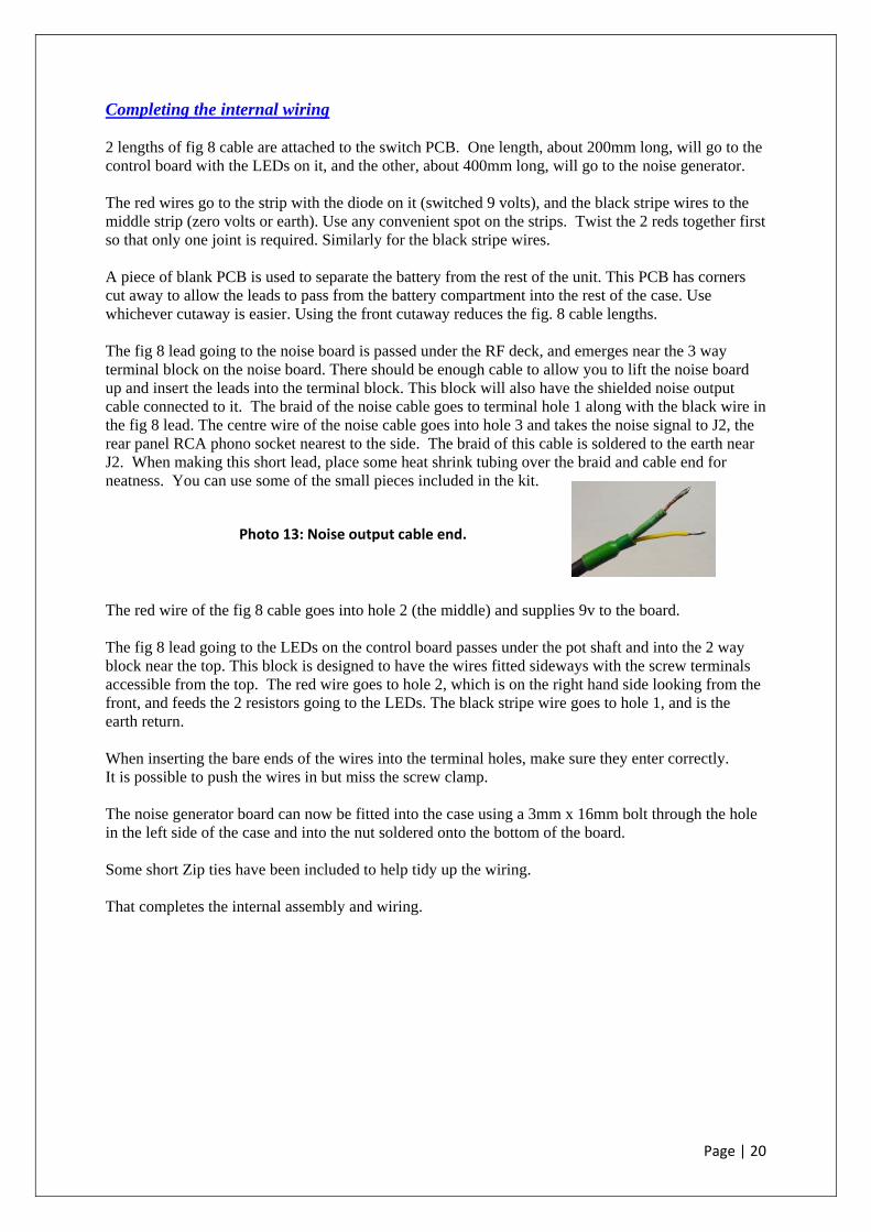
Alternatively, a frequency counter will read somewhere between 400 Hz and 800Hz. It can also be fed into a small amplifier with a 100 times attenuator to drop the level to around 100mV or so. You can check the noise output on an oscilloscope, or listen on a receiver by placing the antenna lead near the generator. Note: if the noise generator is connected to the RF deck, the RF signal voltage amplitude will be quite low as the 3 turn transformer primary has a low impedance. Adjust the noise level trimpot for a healthy level when listening at around 28 MHz. You will find several positions of the trimpot will produce reasonable noise levels. If you notice any low frequency rumble or instability, choose a different setting. If you are using a receiver to listen to the noise, adjust the tone trimpot until you can hear tone modulation on the noise. You can over adjust this control which will drop the overall noise level. You can use a receiver by coupling the output of the noise generator into the antenna of the receiver via a small capacitor of a few pf, or just sitting the receiver antenna lead near the noise board. You will find a position for the tone level which is a good compromise between overall high frequency noise, and tone level. You really only need set it so that it is audible but not over powering the noise. Once the noise generator is working, you can couple it into the RF bridge using a short phono plug to phono plug link. The link is made using 2 RCA phono plugs and a short length shielded audio cable. This cable is easier to solder to the RCA plugs, and over a short distance, this link does not need to be RF coax. Use the centre for the spigot and take the shield to the earth lug. Some small lengths of heat shrink have also been supplied. The larger diameter pieces are placed over the cable ends prior to soldering and the smaller, on the centre spigot to reduce the possibility of shorts. You don’t have to use them, but they can help tidy up the work. Use whichever suits.
Photo 15: Frequency of signal on Q5 collector.
Photo 16: Noise generator output. The level on the waveform is around 9 v peak to peak. Photos show no tone, low tone and high tone levels.

Page | 25
After soldering, check with a meter for shorts. It’s is easy to melt the insulation if you take too long or the lengths are short and tight. Attach a receiver to the “Receiver” SO239 connector and tune it to a suitable frequency such as 3.5MHz or similar. Set it to AM mode and wide bandwidth. You should hear a significant level of noise when you turn the power on to the bridge. Adjust the noise generator tone level for a suitable level of tone and noise. At this stage, turning the dials will not cause a dip. There may be some noise level changes but no dip. Attach a short circuit to the Z unknown connector. You can use a PL259 plug with a short circuit in it. Turning the dials should now produce a dip. The R dial should be at one end, and the C dial will be somewhere towards the centre. Calibration and adjusting the dials. The dial drums can now be adjusted to their approximate positions. Ensure the wood screws in the drums are not fully in. Please note:- Garth Jenkinson, VK3BBK, used modified PL259 plugs with an improved short circuit and the use of SMD resistors to achieve excellent results. These terminations remove the need to solder test components internally - a more convenient method of testing. See DVD for details and photos in folder titled “feedback from kit builders”. Resistance dial. Please note that the low cost 500 ohm potentiometers used in this kit have a resistance tolerance of ±20%. Even better quality pots costing considerably more, are specified as ±10% or so. It is important to bear this in mind when checking the accuracy of the R dial. Each kit has the pot limits measured with a digital meter and every effort is made to use ones which matches the scale included in the kit. The scale provided in the kits was made with a pot measuring 540 ohms across the pot. Some pots have measured as low 520 ohms and some as high as 560 ohms. However, it was noticed that all the above pots were within 4% of the scale values across the range from 0 to 500 ohms. The accuracy is better below 400 ohms (2%), indicating that the potentiometer track linearity is fairly good up to 400 ohms. and only starts to deviate more towards the high resistance end of the pot. Also, please note that scale calibrations are not the DC resistance of the pot. The scale was produced using precision carbon resistors across the Z unknown terminals at a frequency of 1MHz. For example, a 250 ohm precision resistor across the Z unknown connector nulls at the 250 ohm mark on the dial. However a DC ohm meter across the pot actually measures 266 ohms at this dial setting. These differences are caused by various stray impedances within the unit and the test resistor, causing the readings to change with frequency. That is why the bridge needs to be calibrated by using known values across the Z unknown connector at the main frequency of use and not a DC ohmmeter. Some commercial bridges use precision “standards” for calibration prior to use. Others use correction charts. In order to help improve the accuracy of the RX1 bridge, the dials contain a logging scale which can be used in conjunction with external components of known value. The paper dials have been designed

Page | 26
to be easily replaced should you wish to calibrate the unit to suit your needs. PDFs of the dial artwork have been included so that new ones can be easily produced with a home PC and printer. These measures help overcome the limitations of the 2 primary bridge components used in this bridge. This makes for a unit with better resolution than some of the commercial ones which tend to use dial calibrations consisting of thick paint or stencil marks, on the panel behind the knobs. So now proceeding with the calibration, rotate the R drum till the “0” mark on the logging scale lines up with the lid cursor when the pot is fully anticlockwise. You will need to lift the lid several times during this operation. The lid has a recessed lip. Ensure the lip engages with the case correctly so that the cursors are in their correct location. Once the “0” mark is directly under the cursor, carefully tighten the wood screw to stop the drum slipping on the shaft. Rotating the pot fully clockwise should result in the cursor lining up with the “100” mark. It may not be perfectly in line but it should be close enough to ensure the dial calibrations are within 5%. Adjust the drum so the error is equal at each end. The important point to note is that the dial will later be checked against a 49.9 ohm 1% resistor, and it is suggested that 50 ohms dial setting be used to align the cursor with the drum. The logging scale has been provided so that small deviations can be logged and corrections made. Even expensive commercial bridges (non digital ones) use correction charts to correct for errors. All bridges contain various errors due to stray circuit elements both internally and externally, which are very difficult to remove. Correction charts, in conjunction with precision components across the Z unknown terminals, are used for more accurate work. Reactance dial. The next step is to rotate the reactance dial so that the “0” mark of the logging scale is under the cursor when the variable capacitor is turned fully anticlockwise. Tighten the wood screw once this is done. Rotating the dial fully clockwise should result in the “100” on the logging scale under the cursor. The next step is to adjust the internal compensation components. The minimum capacitance is 20pf at the fully clockwise position and is labelled “SET 20pf”. The zero reactance point is about halfway and is labelled “SET ZERO” on the reactance dial. The tuning capacitor has 2 screw driver slot trimmers at the back. These have been set to a give a minimum capacitance of 20 pf using a digital capacitance meter. However a small adjustment may be necessary to cater for small stray variations. Initially, set the small compensation trimmers VC2 and VC4 to minimum. This can be done by looking at the plates and rotating the screwdriver slot for the least overlap. Place a short circuit across the Z unknown terminal by soldering a piece of wire from the centre spigot to the rear panel circuit board nearby. Tune the receiver to a low frequency (1MHz) and set the R dial to zero. Turning the reactance dial should result in a deep null at some spot on the dial. In theory it will be between 90 pf (VC3 at minimum) and 150 pf (VC3 at maximum). If there is no deep null, double check your work.

Page | 27
Assuming you have found a null, adjust VC3 so that the null occurs at the “SET ZERO” mark. This will need further adjustment later once the other trimmers are also adjusted and the “20pf” is checked. The next step is to adjust the compensation coil Lcomp Zu to compensate for stray inductance in the variable resistor/capacitor arm of the bridge. It is unlikely that you will need the compensation coil on the other side of the bridge (Lcomp R). Set the receiver at 1MHz and null the bridge. The R dial should read zero ohms and the X dial should be at, or close to Zero. Now tune the receiver to 28MHz. The reactance dial will null at a different spot. Adjust the coil by stretching or compressing till there is no difference between the reactance zero at 1MHz and 28MHz. You may need to actually shorten the coil by cutting a small length from it. This adjustment may be as small as 2 or 3mm! In one case the coil was reduced to one small turn (see addenda video). In addition, it was found that the Sangean receiver affected the zero setting at 29Mhz when the RF gain pot was turned to minimum. In this receiver, the RF gain control is placed near the antenna input. Also, the antenna input socket has 0.7v dc on it used for external preamps. Adjusting the pot to minimum must be placing a loading on the bridge which in turn affects the bridge transformer. Once the pot is turned off the minimum position, the bridge compensation works correctly. Please note that this effect is only at the higher frequencies. A buffer amp or emitter follower between the bridge and the receiver would probably eliminate this problem. If you find that you cannot move the null in the right direction, it may be just possible that the bridge has too much inductance in the unknown arm of the bridge. In this case put the compensation coil in the variable resistor side of the bridge using the extra PCB pad provided. Refer to the PCB overlay for its location. Move the position of the wire going to the pot to the correct side of the compensation coil. Once there is no variation in the reactance reading for a short circuit load between 1MHz and 28MHz, the bridge is close enough compensated for stray inductance. Having set the reactance scale approximately right, you can now adjust the compensation trimmers for stray capacitance. VC2 is used to cancel stray capacitance on the variable resistor/capacitor side of the bridge. VC4 is used to cancel miscellaneous stray capacitance. However its adjustment also affects the adjustment of VC2. Lift the shorting wire off and solder a small 430/432 ohm resistor (supplied in kit) across the Z unknown connector rear spigot and ground. Tune the receiver to 1MHz and set the R dial to 430/432 ohms. The Reactance dial will be around the zero mark. Adjust VC2 so that the R dial nulls at 430/432 ohms. You can rock the reactance dial for a deeper null. You may need to do this several times, rocking the dial back and forth looking for the best null. Confirm the 430/432 ohm R dial setting by rocking it back and forth also. Now check the setting at a high frequency such as 28 MHz. Readjust VC2 carefully to set the R scale at 430/432 ohms, and then swing VC4 so that the reactance scale reads near zero. Adjusting VC4 can shift the setting for VC2. Generally, VC2 sets the R dial at a low frequency, and VC4 sets the X dial at the high frequency.

Page | 28
You will probably find that the zero reactance point has shifted slightly so put the short circuit back and adjust VC3 a little to bring it back to zero. For now, these adjustments should compensate for stray capacitance. Now check the lower limit of 20pf on the X dial. This is best done by soldering a 20pf good quality capacitor across the Z unknown connector spigot and earth. 2 off 10pf (±2%) NPO ceramic capacitors have been included in the kit. Solder one capacitor across the Z unknown connector. Use only one capacitor in case the lower limit is between 10pf and 20pf. With the R dial at zero, try to null the bridge using the X dial at a low frequency such as 1MHz. The null should be below the 20pf mark and should be just out of reach. Now connect the second 10pf capacitor in parallel so that there is now a total of 20 pf across the Zunknown connector. The bridge should now just hit the null point at the “Set 20pf” on the dial. If not, carefully adjust one of the 2 trimmers on the rear of the tuning capacitor VC1 so that the null occurs on the “Set 20pf” mark. This adjustment can be a little broad so an approximate position should be acceptable. The trimmers are somewhat obstructed by the RF deck PCB so some judicial tweaking may be needed here. However, you will probably find it is close enough as these trimmers have been preset for you. This should now have set the lower limit to 20pf. The overall tolerance of the 2 test capacitors in parallel is ±2% so the error should only be around ±0.4pf . You can now go back and check all the settings by repeating the previous steps. Again, the zero reactance with a short may have moved so again adjust VC3 to correct the zero point with a short circuit. Once you have set the compensation trimmers and coil for 1Mhz and 28MHz, you can double check the resistance dial at 50 ohms. Solder a 49.9 ohm resistor across the Zunknown connector and check that the R dial lines up at 50 ohm. If it is slightly out, you can rotate the dial drum so that the cursor lines up with 50 ohm. This is around the most common value of resistance the bridge will most likely measure so it may be better to set the dial as accurately as possible at this resistance value. After several repetitions of the adjustments, the bridge dials should be reasonably accurate. You can check these with various non inductive resistors across Z unknown. For some bridge measurements, it will be necessary to produce a short circuit inside a PL259 plug so that it can be plugged into the bridge rather than having to solder the short inside the bridge. The same applies to various test resistors. These will be satisfactory at low frequencies but you will find that they can produce some reactance readings and resistance shifts at 28MHz. This can be due to several factors. These include stray capacitance and inductance in the PL259 plugs and the actual resistors themselves. (See documentation on DVDs for improved PL259 terminations by Garth, VK3BBK). Typically, the PL259 plug can have around 2pf capacitance (mostly in parallel) which can affect the reactance readings. RF resistance (skin effect) can also affect the resistance reading.

Page | 29
However, these terminations are necessary for various measurements and one needs to be mindful of errors that can be introduced by the stray components. In most cases the errors will be only a few percent. If you wish to check the calibration of the dials, or produce ones more suited to your needs, the “+C” portion of the reactance dial can be calibrated using good quality mica capacitors placed across the Z unknown connector. The same capacitors can also be used for the “-C” portion of the reactance dial. In this case the capacitor is placed across the internal Cs capacitor, and a 50 ohm resistor is connected across the Z unknown connector to ground. Use a frequency that you want to calibrate the bridge for. Use of a low frequency helps reduce the stray capacitance and inductance in the test capacitor. You can also use a good quality piece of coax to produce known values of reactance at various frequencies. Please refer to reference 1, “The ARRL Antenna handbook 17th edition”, for details of this method. Some bridge designs change the value of the series capacitor so as to extend the reactance ranges. Increasing it (>120pf) will extend the capacitance range by shifting the zero reactance point on the dial clockwise. For example, a 200pf internal series capacitor will shift the variable capacitor zero null to 200pf, which is near the end of its travel clockwise. So the +C range becomes more spread out. Decreasing it (<120pf) will shift the zero reactance point anticlockwise so as to provide a greater range of inductive reactance. In this case the bridge nulls with less variable C thereby increasing the –C range portion of the dial. These various designs use switches or relays to add or remove capacitors in the circuit. However, it was found that the bridge could not be accurately calibrated with the additional components being switched in and out of circuit. The dials became too inaccurate under these conditions and it was decided not to provide range extension in this manner. However, the range provided by this design covers the most typical impedance ranges. However, if you wish, you can extend the range by adding external range extending components at the Z unknown connector. For example, a small 5-50pf trimmer mounted in a plug/socket adapter, in series with the test load, and the Z unknown connector, can be added so as to extend the inductance range. The 50pf trimmer set to 40pf, will now be in series with the internal 120pf capacitor thereby decreasing the effective value to 30pf. In this case, the trimmer is adjusted, with a short circuit test termination plugged into the extender, so that it nulls at the 30pf mark on the +C dial. This will extend the -C range. You will need to recalibrate the dial (using the logging scale) for the new range using known values of inductance, or inductive reactance as test terminations. Extending the range may help if you are measuring antenna impedances which contain high values of inductive reactance. In cases like that, it may not be necessary to know the exact value of the antenna impedance. An estimate of the value is sufficient, as you will be adjusting the antenna for resonance, and thereby

Page | 30
correcting for the large deviation. The exact value is not really required – just an estimate will suffice. If you require more accurate dials, the ones supplied can be replaced with custom made ones. For some applications you may want to use easier to read simplified scales. These can be easily produced using a CAD or drawing program and printing the scale on a home printer. This may also be necessary if you replace the variable capacitor and potentiometer with other values more suited to your needs. You can temporarily attach a strip of 1mm graph paper around the drum and note which “mm” section of the strip represents your calibration points. The strip can then be removed and the mm marks transferred into a CAD program to produce a neat scale. Using removable strips around a dial drum in this manner simplifies re calibration and produces good results. Once the dials are set, you can tidy up the area around the Z unknown connector by removing any shorts and resistors. Also, you can carefully adjust the dial LEDs so that a nice headlight shape beam is illuminating the dials. Bending the LED leads is a little finicky but by putting an “S” bend in the leads, you can adjust it such that a nice beam is produced. Pushing the lid on may disturb your “bending” but with a little patience you should be able to get a reasonable beam. The LEDs are really for effect and don’t really contribute anything significant to the operation of the bridge. The dials are visible without the LEDs but the LEDs add some interest if nothing else. Finally place some foam packing around the battery so that it does not rattle around and also to protect the switch area. You have now completed the construction of the bridge. Using the Bridge. The bridge can be used for a variety of RF impedance measurements. The kit comes with a series of spreadsheets which you can use to perform various measurements on coaxial cable and HF antennae. The spreadsheets are made using the Excel program in Microsoft Office 2007. The files have been saved in Office 2003 format. The first 2 spreadsheets allow you to find reactance values at various frequencies from the dial readings. The remainder are used for coaxial cable parameters and measuring antenna impedance at the end of a coax cable length. You can also use the bridge in conjunction with a smith chart to make various measurements and produce impedance transformers and antenna tuning elements. There are also some very good transmission line programs on the web you can use. Some website addresses have been added to the reference list. In addition to measuring cable characteristics and antenna impedances, you can also use the bridge for checking the operation of Baluns, find small values of inductance, capacitance, RF resistance, tuned circuit frequencies, and so on. There is plenty of literature available describing the use of the bridge. Also, you can use an external signal generator by unplugging the internal noise source and feeding it into the bridge. In this case, the detector can be a RF voltmeter (diode detector with DC amplifier etc.).
Page | 31
References: 1. The ARRL antenna handbook, 17th edition, ARRL, Newington, Connecticut, 1994, Section 27-23. 2. John Grebenkemper, KI6WX, “Improving and using R-X Noise Bridges”. QST August 1989, page 27. 3. Lloyd Butler, VK5BR, “A few tips on the design of the noise bridge”, Amateur Radio, February 1990, Page. 6.
4. Leonard H. Anderson, “antenna bridge calculations” Ham Radio May 1978, page 34. 5. John J. Nagle, “rf impedance bridge measurement errors and corrections”, Ham Radio May 1979, page.22. 6. Robert A. Hubbs, W6BXI, and A. Frank Doting, W6NKU, “improvements to the RX bridge” Ham Radio February, 1977, page. 10 7. Walter C. Johnson, “Transmission Lines and Networks”, International Student edition, McGraw-Hill, New York, 1950. Used for transmission line theory and equations. 8. Wilfred N. Caron, “Antenna Impedance Matching”, ARRL, Newington, Connecticut, 1989. ISBN: 0-87259-220-0 ======================================================================= Websites with transmission line calculators and additional information: http://fermi.la.asu.edu/w9cf/tran/ http://www.ac6la.com/index.html http://pagesperso-orange.fr/rulivas/downloads.htm http://vk1od.net/calc/nbc1.htm http://vk1od.net/measurement/NoiseBridge/RX1i.htm UPDATED 12/01/2010: Items added or updated:‐ Commercial PCBs; Use of brass shaft coupler for Vc; Test terminations by Garth Jenkinson, VK3BBK UPDATED 12/04/2011: Web address for VK1OD’s RX1/RX2 website calculator tool. UPDATED 7/07/2011: Web address for VK1OD’s low R linearity improvement. UPDATED 20/09/2012: Change of address. ======================================================================
VK3AQZKITS 225 Wilsons Road, Cape Paterson
PO BOX 167, Wonthaggi, Vic. AUSTRALIA, 3995
Tel: +61 03 5998 1188 Fax: as above Email: [email protected] Web: www.vk3aqzkits.com