virtex ii architecture · virtex-ii architecture 18kb bram cam multiplier blvds backplane pci-x ddr...
TRANSCRIPT
Virtex II Architecture
Rev 4 –March 4th. 2002 – J-L Brelet - All right reserved - © XILINX 2002
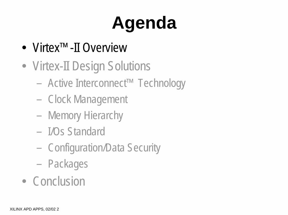
Agenda• Virtex™-II Overview• Virtex-II Design Solutions
– Active Interconnect™ Technology– Clock Management– Memory Hierarchy– I/Os Standard– Configuration/Data Security – Packages
• Conclusion
XILINX APD APPS, 02/02 2
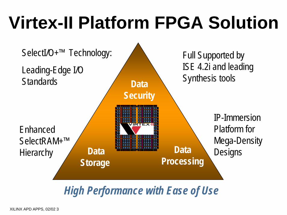
Virtex-II Platform FPGA Solution
Data Storage
Data Processing
Data Security
Full Supported by ISE 4.2i and leading Synthesis tools
SelectI/O+™ Technology:
Leading-Edge I/O Standards
Enhanced SelectRAM+™ Hierarchy
IP-Immersion Platform for Mega-Density Designs
High Performance with Ease of UseXILINX APD APPS, 02/02 3
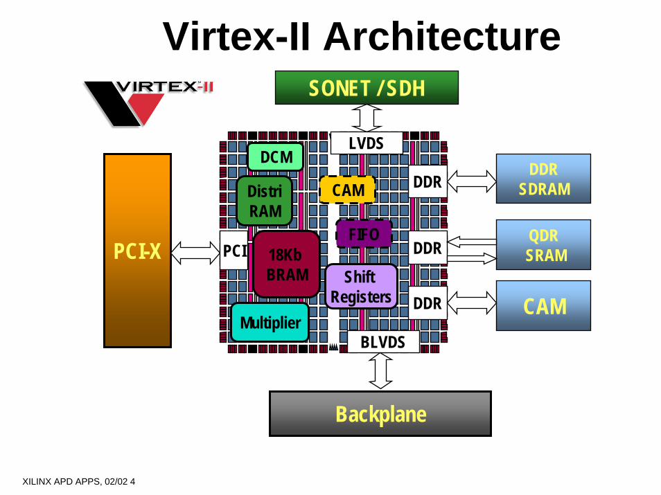
Virtex-II Architecture
18Kb BRAM
CAM
MultiplierBLVDS
Backplane
PCI-X
DDR
DDR
DDR
CAM
QDRSRAM
DDRSDRAMDistri
RAM
LVDS
Shift Registers
DCM
FIFOPCI
SONET / SDH
XILINX APD APPS, 02/02 4
Agenda•Virtex-II Overview•Virtex-II Architecture– Active interconnect technology– Clock management– I/O standards– Memory hierarchy– Configuration/data security – Packages• Conclusion
XILINX APD APPS, 02/02 5

Active Interconnect Technology• Interconnect an array of switch matrices• All Virtex II features can access routing resources
through the switch matrix– Simplify design and place & route
SwitchMatrix
CLB
SwitchMatrix
SwitchMatrix
SwitchMatrix
18KbBRAM
SwitchMatrix
SwitchMatrix
IOB MULT 18x18
SwitchMatrix
DCM
XILINX APD APPS, 02/02 6
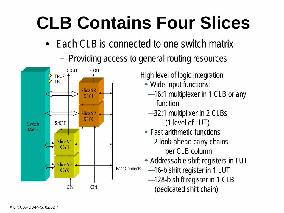
CLB Contains Four Slices• Each CLB is connected to one switch matrix
– Providing access to general routing resources
CIN
SwitchMatrix
TBUFTBUF
COUTCOUT
Slice S0X0Y0
Slice S1X0Y1
Fast Connects
Slice S2X1Y0
Slice S3X1Y1
CIN
SHIFT
High level of logic integrationWide-input functions:
—16:1 multiplexer in 1 CLB or anyfunction
—32:1 multiplixer in 2 CLBs (1 level of LUT)
Fast arithmetic functions—2 look-ahead carry chains
per CLB columnAddressable shift registers in LUT
—16-b shift register in 1 LUT—128-b shift register in 1 CLB
(dedicated shift chain)
XILINX APD APPS, 02/02 7
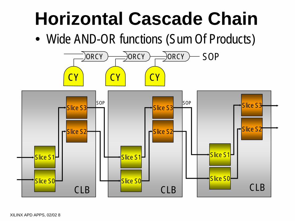
Horizontal Cascade Chain • Wide AND-OR functions (Sum Of Products)
CY CY CY
ORCYORCYORCY SOP
SOP
Slice S0
Slice S1
Slice S2
Slice S3
CLBSlice S0
Slice S1
Slice S2
Slice S3
CLBSlice S0
Slice S1
Slice S2
Slice S3
CLB
SOP
XILINX APD APPS, 02/02 8
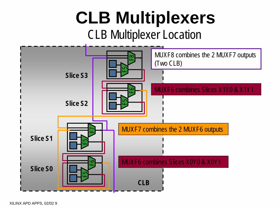
CLB Multiplexers CLB Multiplexer Location
F5F8
F5F6
CLB
Slice S3
Slice S2
Slice S0
Slice S1 F5F7
F5F6
MUXF8 combines the 2 MUXF7 outputs (Two CLB)
MUXF6 combines Slices X1Y0 & X1Y1
MUXF7 combines the 2 MUXF6 outputs
MUXF6 combines Slices X0Y0 & X0Y1
XILINX APD APPS, 02/02 9
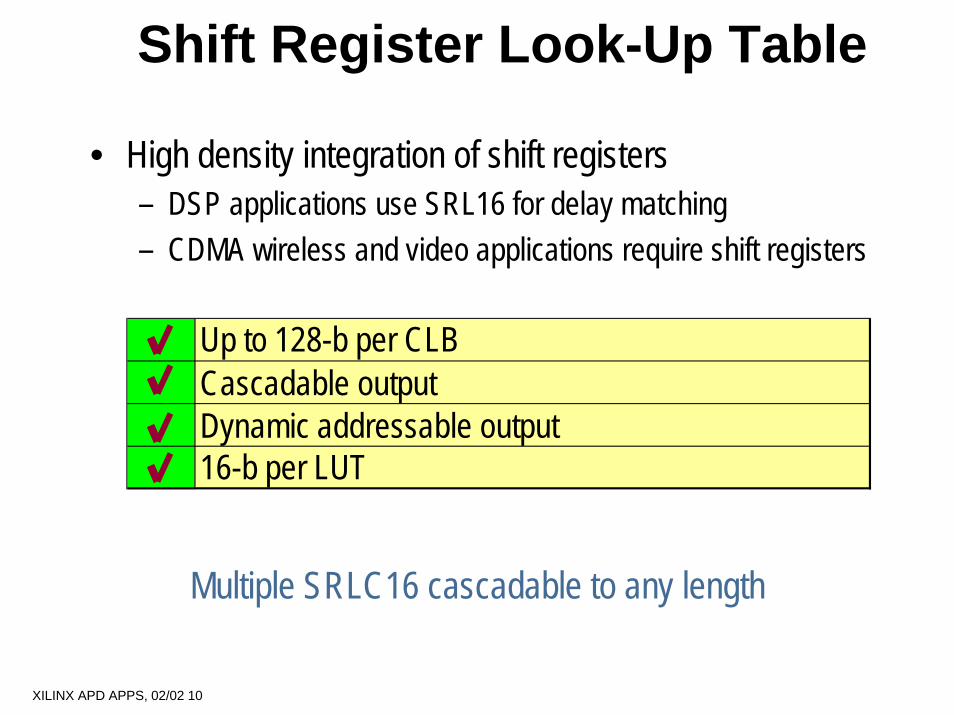
Shift Register Look-Up Table
• High density integration of shift registers– DSP applications use SRL16 for delay matching– CDMA wireless and video applications require shift registers
Up to 128-b per CLBCascadable outputDynamic addressable output16-b per LUT
Multiple SRLC16 cascadable to any length
XILINX APD APPS, 02/02 10
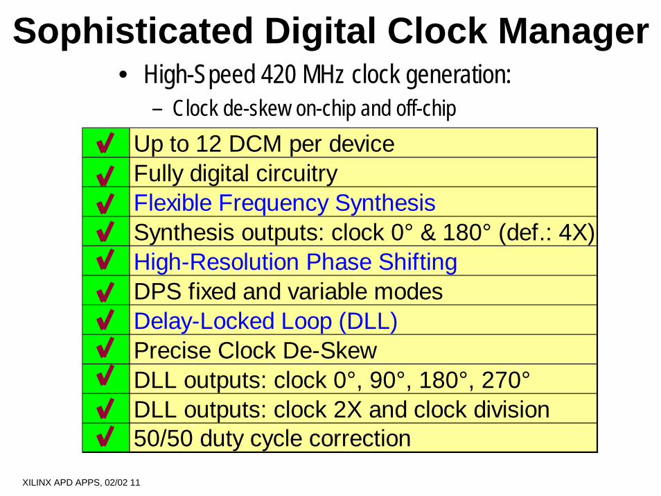
Sophisticated Digital Clock Manager• High-Speed 420 MHz clock generation:
– Clock de-skew on-chip and off-chipUp to 12 DCM per deviceFully digital circuitryFlexible Frequency Synthesis Synthesis outputs: clock 0° & 180° (def.: 4X)High-Resolution Phase ShiftingDPS fixed and variable modesDelay-Locked Loop (DLL)Precise Clock De-SkewDLL outputs: clock 0°, 90°, 180°, 270°DLL outputs: clock 2X and clock division 50/50 duty cycle correction
XILINX APD APPS, 02/02 11
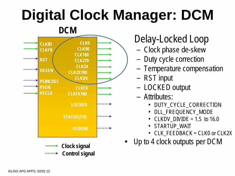
Digital Clock Manager: DCMDelay-Locked Loop – Clock phase de-skew– Duty cycle correction– Temperature compensation– RST input – LOCKED output– Attributes:
• DUTY_CYCLE_CORRECTION• DLL_FREQUENCY_MODE • CLKDV_DIVIDE = 1.5 to 16.0• STARTUP_WAIT• CLK_FEEDBACK = CLK0 or CLK2X
• Up to 4 clock outputs per DCM
CLKINCLKFB
RST
CLK0CLK90
CLK180CLK270
CLKDV
LOCKED
CLKFX180PSEN CLKFX
PSDONE
CLK2X180
PSINCDEC
STATUS[7:0]
DSSEN
PSCLK
CLK2X
DCM
Clock signalControl signal
XILINX APD APPS, 02/02 12
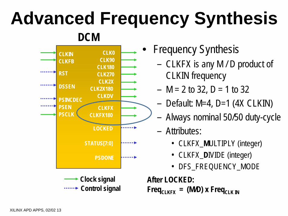
Advanced Frequency Synthesis• Frequency Synthesis
– CLKFX is any M / D product of CLKIN frequency
– M = 2 to 32, D = 1 to 32– Default: M=4, D=1 (4X CLKIN)– Always nominal 50/50 duty-cycle– Attributes:
• CLKFX_MULTIPLY (integer)• CLKFX_DIVIDE (integer)• DFS_FREQUENCY_MODE
After LOCKED: FreqCLKFX = (M/D) x FreqCLK IN
CLKINCLKFB
RST
CLK0CLK90
CLK180CLK270
CLKDV
LOCKED
CLKFX180PSEN CLKFX
PSDONE
CLK2X180
PSINCDEC
STATUS[7:0]
DSSEN
PSCLK
CLK2X
DCM
Clock signalControl signal
XILINX APD APPS, 02/02 13

High Resolution Phase ShiftingFine Phase Shifting– Applies to all CLK outputs– Phase shift = fraction CLKIN period– Fixed or variable modes– Inputs in variable mode:
• PSINCDEC input =Increase /Decrease• PSEN = Enable Phase Shift• PSCLK synchronizes Phase Shift
– PSDONE output– Attributes:
• CLOCKOUT_PHASE_SHIFT =NONE, FIXED, VARIABLE
• PHASE_SHIFT (signed integer)-255 to +255
CLKINCLKFB
RST
CLK0CLK90
CLK180CLK270
CLKDV
LOCKED
CLKFX180PSEN CLKFX
PSDONE
CLK2X180
PSINCDEC
STATUS[7:0]
DSSEN
PSCLK
CLK2X
DCM
Clock signalControl signal
XILINX APD APPS, 02/02 14
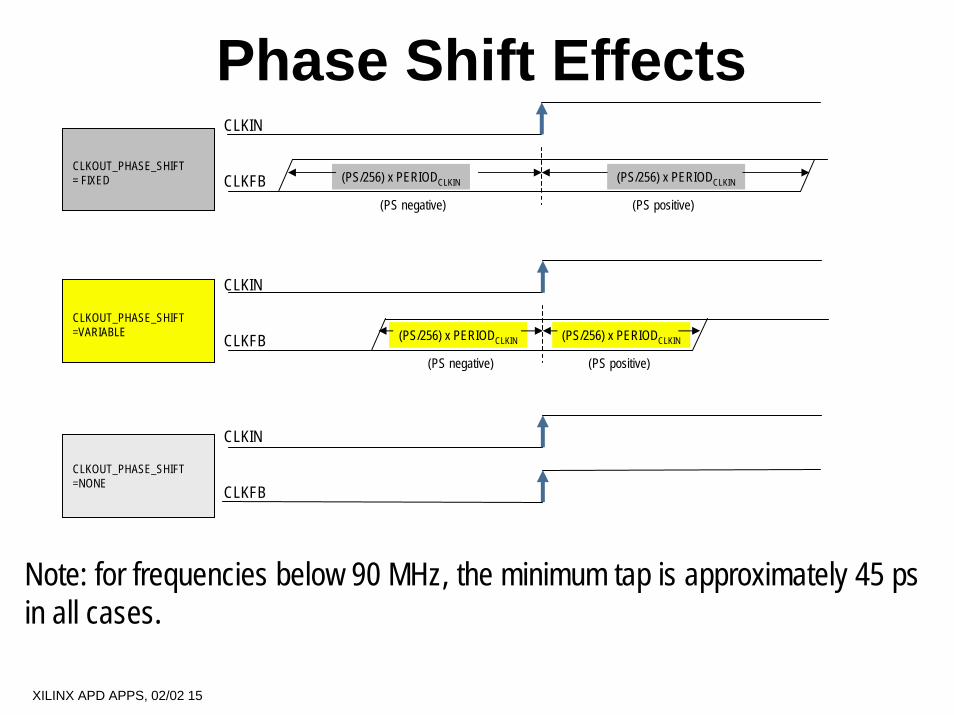
Phase Shift EffectsCLKIN
CLKFB (PS/256) x PERIODCLKIN (PS/256) x PERIODCLKIN
(PS negative) (PS positive)
CLKOUT_PHASE_SHIFT= FIXED
CLKIN
CLKFBCLKOUT_PHASE_SHIFT=VARIABLE (PS/256) x PERIODCLKIN (PS/256) x PERIODCLKIN
(PS negative) (PS positive)
CLKIN
CLKFBCLKOUT_PHASE_SHIFT=NONE
Note: for frequencies below 90 MHz, the minimum tap is approximately 45 ps in all cases.
XILINX APD APPS, 02/02 15
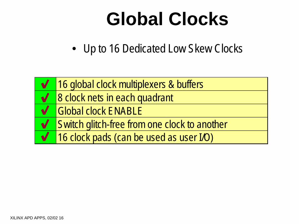
Global Clocks• Up to 16 Dedicated Low Skew Clocks
16 global clock multiplexers & buffers8 clock nets in each quadrantGlobal clock ENABLESwitch glitch-free from one clock to another16 clock pads (can be used as user I/O)
XILINX APD APPS, 02/02 16
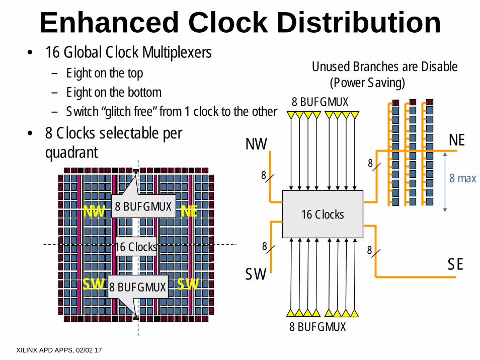
Enhanced Clock Distribution• 16 Global Clock Multiplexers
– Eight on the top – Eight on the bottom– Switch “glitch free” from 1 clock to the other
• 8 Clocks selectable per quadrant
8 BUFGMUX
16 Clocks
8
88
8
SE
NENW
SW
8 BUFGMUX
8 max
NW
SW
NE
SW
16 Clocks
8 BUFGMUX
8 BUFGMUX
Unused Branches are Disable (Power Saving)
XILINX APD APPS, 02/02 17

Global Clocks: BUFGMUX• Three modes:
– Clock buffer • Low skew clock distribution• BUFG primitive
– Clock enable• Stop the clock High or Low• BUFGCE (stop Low)
– Clock multiplexer “glitch-free”• Switch from one clock to another• BUFGMUX
OIBUFG
BUFG
MUX
OI1
I0
S
OI
CE
BUFGCE
• unrelated clocks
CLK0
CLK1
SEL
OUT
Wait for low
SwitchNo pulse width shorter than
1/2 of the period
XILINX APD APPS, 02/02 18
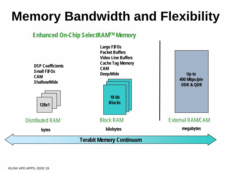
Memory Bandwidth and FlexibilityEnhanced On-Chip SelectRAMTM Memory
Large FIFOs Packet BuffersVideo Line BuffersCache Tag MemoryCAMDeep/Wide Up to
400 Mbps/pin DDR & QDR
DSP CoefficientsSmall FIFOsCAMShallow/Wide
18 kbBlocks128x1
Block RAM External RAM/CAMDistributed RAMmegabyteskilobytesbytes
Terabit Memory Continuum
XILINX APD APPS, 02/02 19
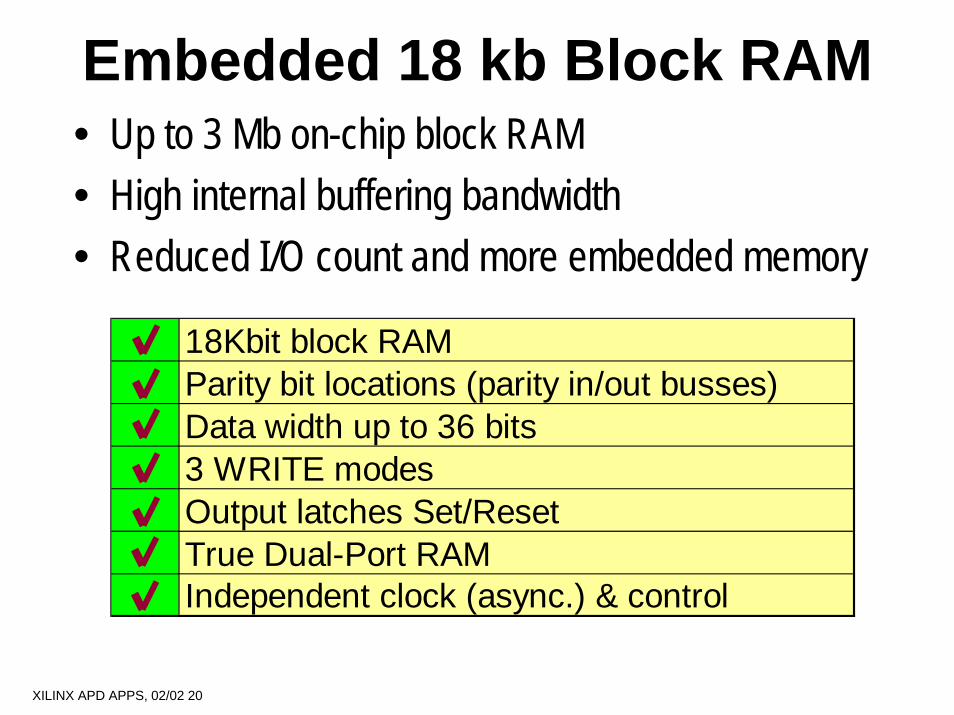
Embedded 18 kb Block RAM• Up to 3 Mb on-chip block RAM• High internal buffering bandwidth• Reduced I/O count and more embedded memory
18Kbit block RAMParity bit locations (parity in/out busses)Data width up to 36 bits3 WRITE modesOutput latches Set/ResetTrue Dual-Port RAMIndependent clock (async.) & control
XILINX APD APPS, 02/02 20
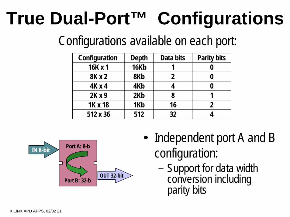
True Dual-Port™ ConfigurationsConfigurations available on each port:
Configuration Depth Data bits Parity bits16K x 1 16Kb 1 08K x 2 8Kb 2 04K x 4 4Kb 4 02K x 9 2Kb 8 1
1K x 18 1Kb 16 2512 x 36 512 32 4
• Independent port A and B configuration:– Support for data width
conversion including parity bits
Port A: 8-bIN 8-bit
OUT 32-bitPort B: 32-b
XILINX APD APPS, 02/02 21
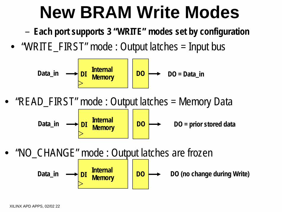
New BRAM Write Modes– Each port supports 3 “WRITE” modes set by configuration
• “WRITE_FIRST” mode : Output latches = Input bus
Internal Memory DOData_in DO = Data_inDI
• “READ_FIRST” mode : Output latches = Memory DataInternal Memory DOData_in DO = prior stored dataDI
• “NO_CHANGE” mode : Output latches are frozenInternal Memory DOData_in DO (no change during Write)DI
XILINX APD APPS, 02/02 22
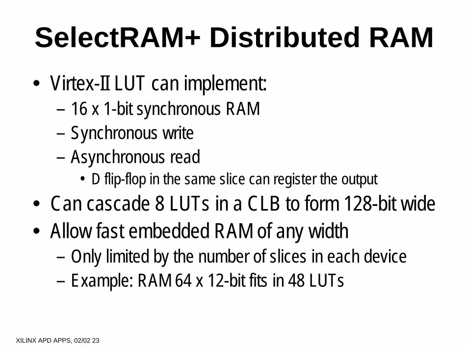
SelectRAM+ Distributed RAM• Virtex-II LUT can implement:
– 16 x 1-bit synchronous RAM– Synchronous write– Asynchronous read
• D flip-flop in the same slice can register the output• Can cascade 8 LUTs in a CLB to form 128-bit wide • Allow fast embedded RAM of any width
– Only limited by the number of slices in each device– Example: RAM 64 x 12-bit fits in 48 LUTs
XILINX APD APPS, 02/02 23
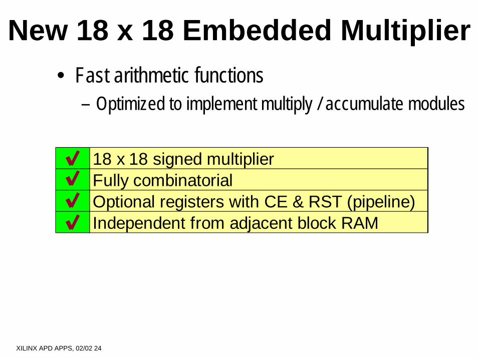
New 18 x 18 Embedded Multiplier• Fast arithmetic functions
– Optimized to implement multiply / accumulate modules
18 x 18 signed multiplierFully combinatorialOptional registers with CE & RST (pipeline)Independent from adjacent block RAM
XILINX APD APPS, 02/02 24
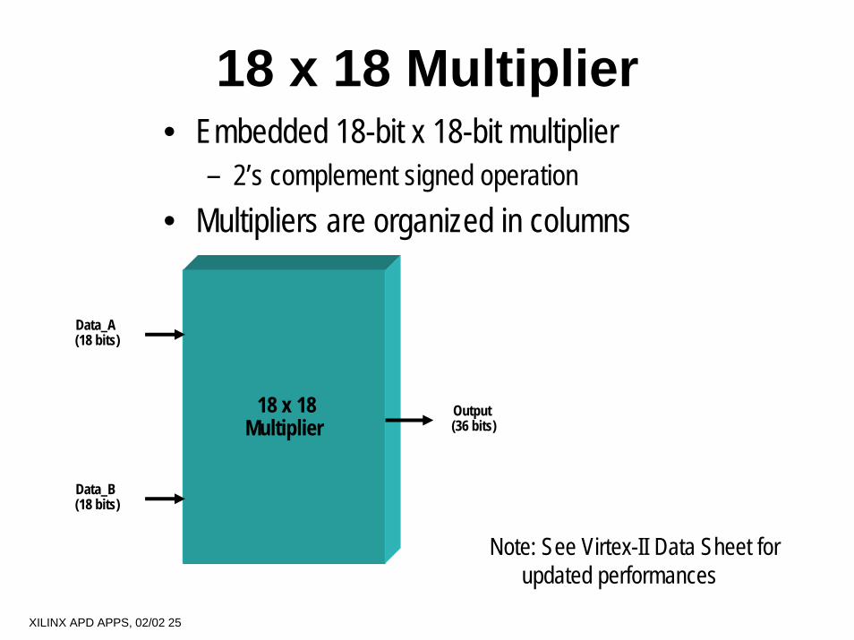
18 x 18 Multiplier • Embedded 18-bit x 18-bit multiplier
– 2’s complement signed operation• Multipliers are organized in columns
18 x 18Multiplier
Output (36 bits)
Data_A (18 bits)
Data_B (18 bits)
Note: See Virtex-II Data Sheet for updated performances
XILINX APD APPS, 02/02 25
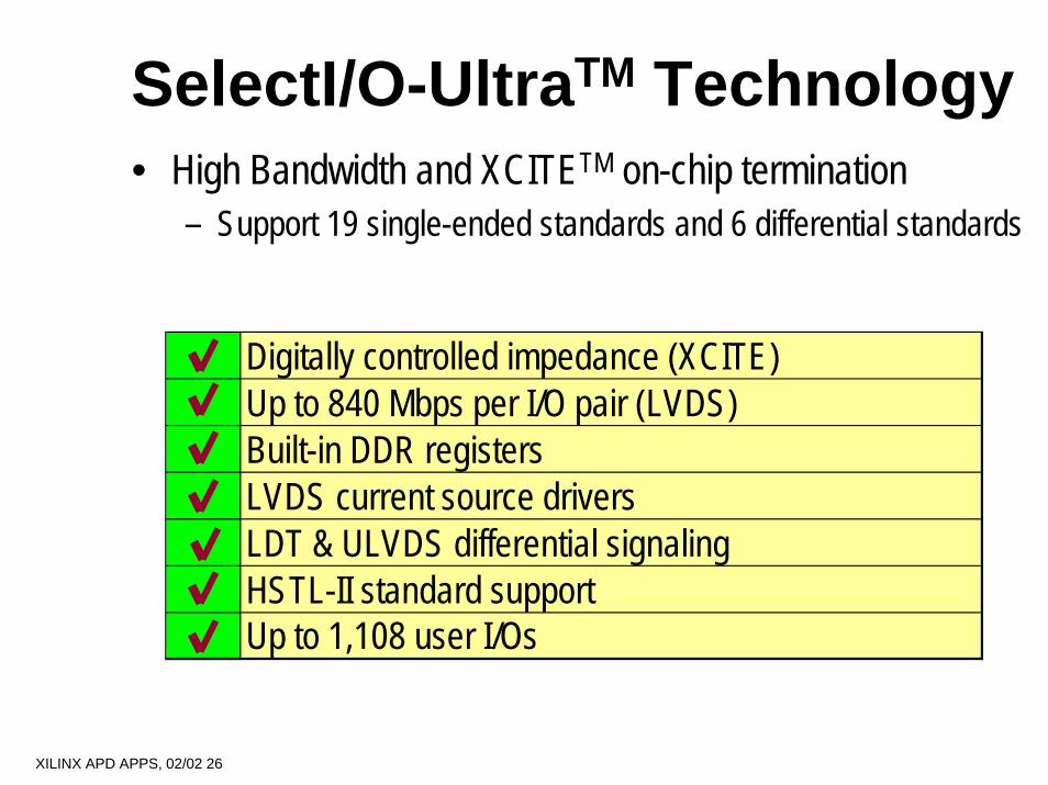
SelectI/O-UltraTM Technology• High Bandwidth and XCITETM on-chip termination
– Support 19 single-ended standards and 6 differential standards
Digitally controlled impedance (XCITE)Up to 840 Mbps per I/O pair (LVDS)Built-in DDR registersLVDS current source driversLDT & ULVDS differential signalingHSTL-II standard supportUp to 1,108 user I/Os
XILINX APD APPS, 02/02 26
High-Speed Interface Design
• Leading edge FPGA I/O performance at 840 Mbps• Support latest hot communication interface protocols,
including:– PCI-X 133 MHz– RapidI/O™ support– POS PHY Level 4 (16 bits/clk @ 832 Mbps), SPI-4– Lightening Data Transport (LDT) support
XILINX APD APPS, 02/02 27
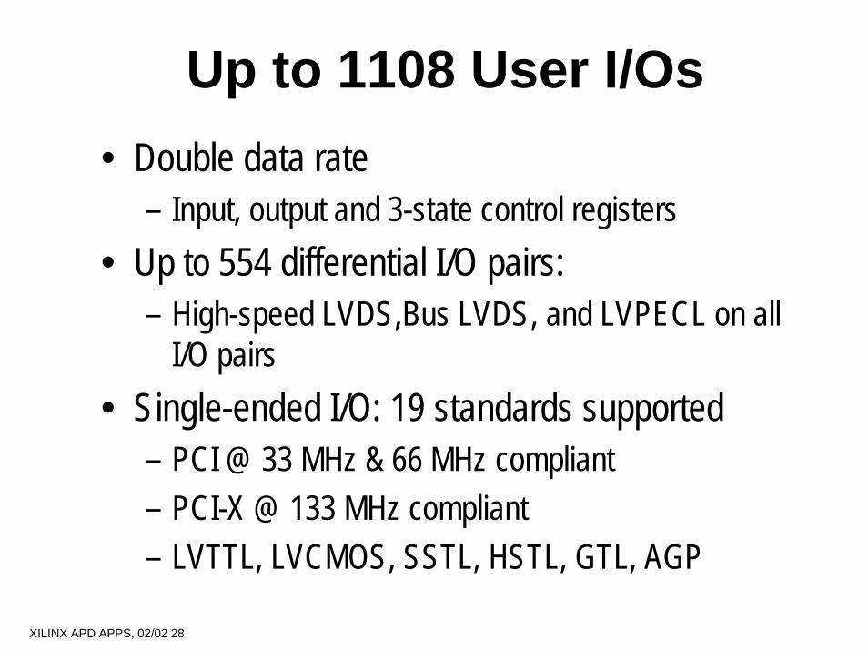
Up to 1108 User I/Os• Double data rate
– Input, output and 3-state control registers • Up to 554 differential I/O pairs:
– High-speed LVDS,Bus LVDS, and LVPECL on all I/O pairs
• Single-ended I/O: 19 standards supported– PCI @ 33 MHz & 66 MHz compliant – PCI-X @ 133 MHz compliant– LVTTL, LVCMOS, SSTL, HSTL, GTL, AGP
XILINX APD APPS, 02/02 28
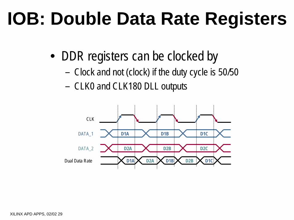
IOB: Double Data Rate Registers
• DDR registers can be clocked by– Clock and not (clock) if the duty cycle is 50/50– CLK0 and CLK180 DLL outputs
DATA_1
CLK
DATA_2
Dual Data Rate
D1A D1B D1C
D2A D2B D2C
D1A D2A D1B D2B D1C
XILINX APD APPS, 02/02 29
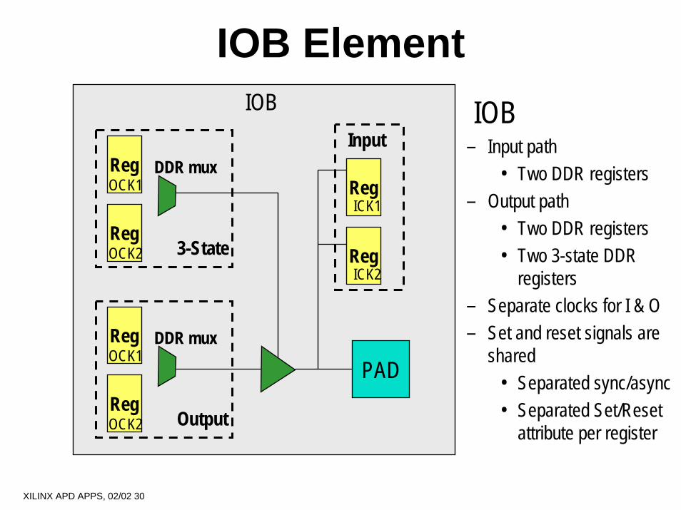
IOB Element
Reg
Reg
DDR mux
3-State
OCK1
OCK2
Reg
Reg
DDR mux
Output
OCK1
OCK2
PAD
Reg
Reg
Input
ICK1
ICK2
IOB IOB– Input path
• Two DDR registers– Output path
• Two DDR registers• Two 3-state DDR
registers– Separate clocks for I & O– Set and reset signals are
shared• Separated sync/async• Separated Set/Reset
attribute per register
XILINX APD APPS, 02/02 30
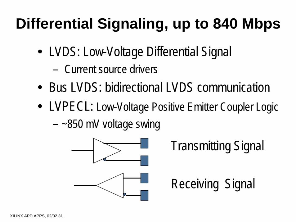
Differential Signaling, up to 840 Mbps
• LVDS: Low-Voltage Differential Signal – Current source drivers
• Bus LVDS: bidirectional LVDS communication• LVPECL: Low-Voltage Positive Emitter Coupler Logic
– ~850 mV voltage swing
Transmitting Signal
Receiving Signal
XILINX APD APPS, 02/02 31
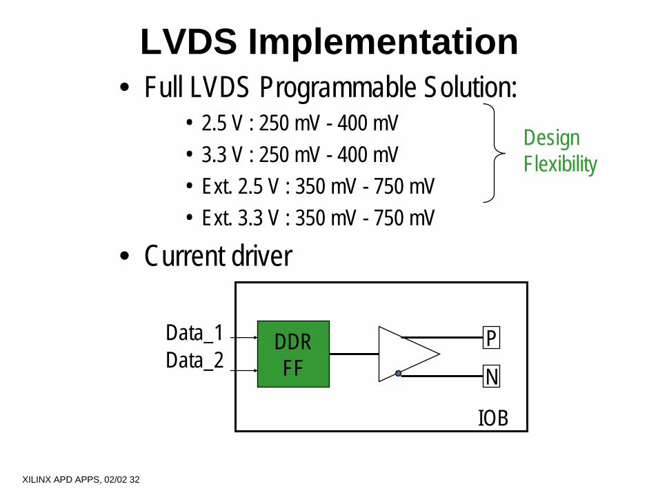
• Full LVDS Programmable Solution:• 2.5 V : 250 mV - 400 mV• 3.3 V : 250 mV - 400 mV• Ext. 2.5 V : 350 mV - 750 mV• Ext. 3.3 V : 350 mV - 750 mV
• Current driver
LVDS Implementation
P
NDDRFF
Data_1Data_2
IOB
DesignFlexibility
XILINX APD APPS, 02/02 32
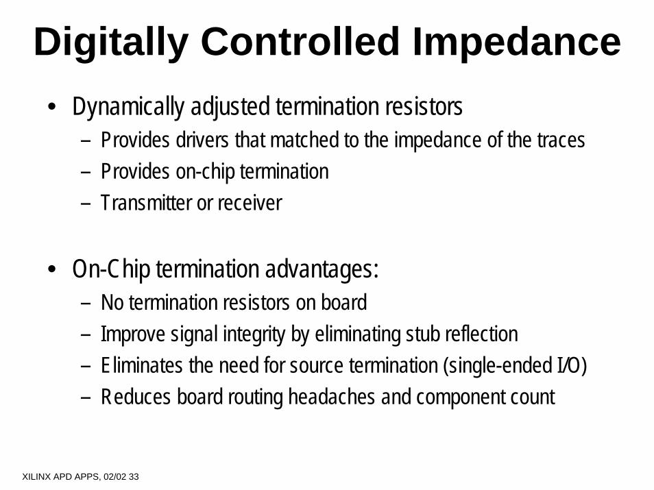
Digitally Controlled Impedance• Dynamically adjusted termination resistors
– Provides drivers that matched to the impedance of the traces– Provides on-chip termination– Transmitter or receiver
• On-Chip termination advantages:– No termination resistors on board– Improve signal integrity by eliminating stub reflection– Eliminates the need for source termination (single-ended I/O)– Reduces board routing headaches and component count
XILINX APD APPS, 02/02 33
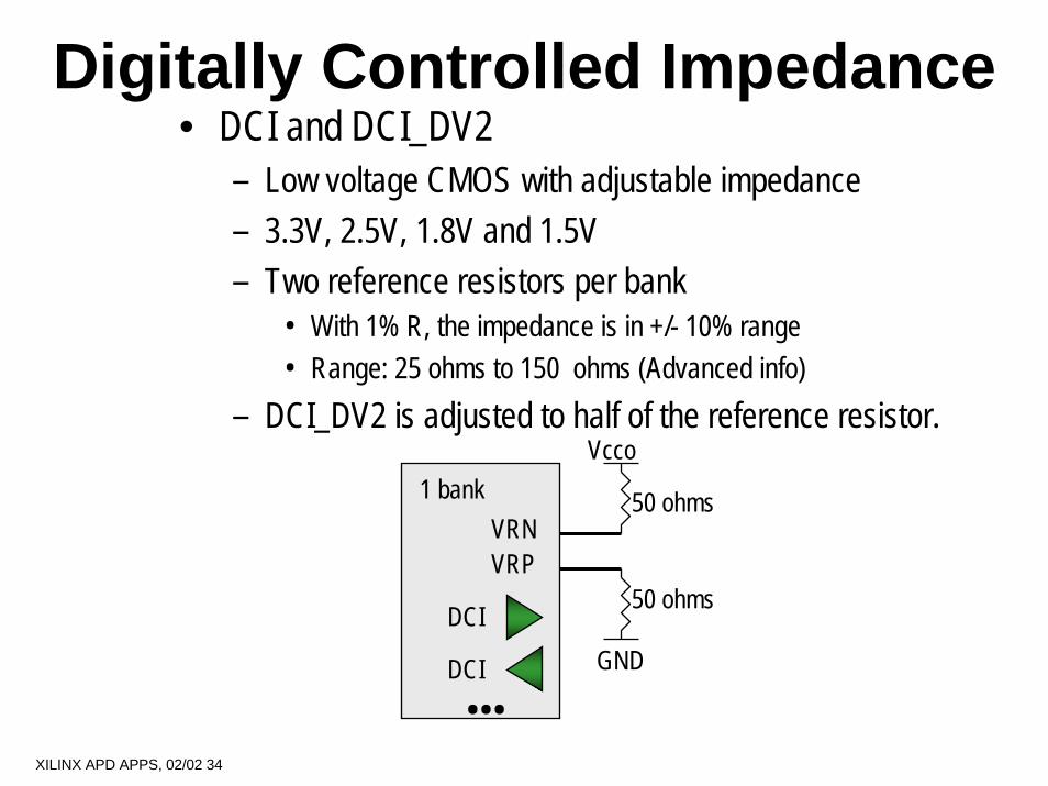
• DCI and DCI_DV2 – Low voltage CMOS with adjustable impedance– 3.3V, 2.5V, 1.8V and 1.5V – Two reference resistors per bank
• With 1% R, the impedance is in +/- 10% range• Range: 25 ohms to 150 ohms (Advanced info)
– DCI_DV2 is adjusted to half of the reference resistor.
Digitally Controlled Impedance
Vcco
GND
50 ohms
50 ohms
VRNVRP
DCI
1 bank
DCI
...XILINX APD APPS, 02/02 34
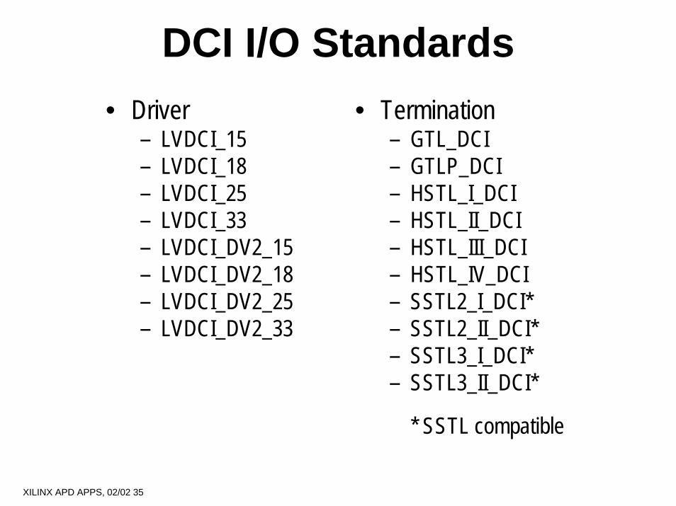
DCI I/O Standards• Driver
– LVDCI_15– LVDCI_18– LVDCI_25– LVDCI_33– LVDCI_DV2_15– LVDCI_DV2_18– LVDCI_DV2_25– LVDCI_DV2_33
• Termination– GTL_DCI– GTLP_DCI– HSTL_I_DCI– HSTL_II_DCI– HSTL_III_DCI– HSTL_IV_DCI– SSTL2_I_DCI*– SSTL2_II_DCI*– SSTL3_I_DCI*– SSTL3_II_DCI*
* SSTL compatible
XILINX APD APPS, 02/02 35
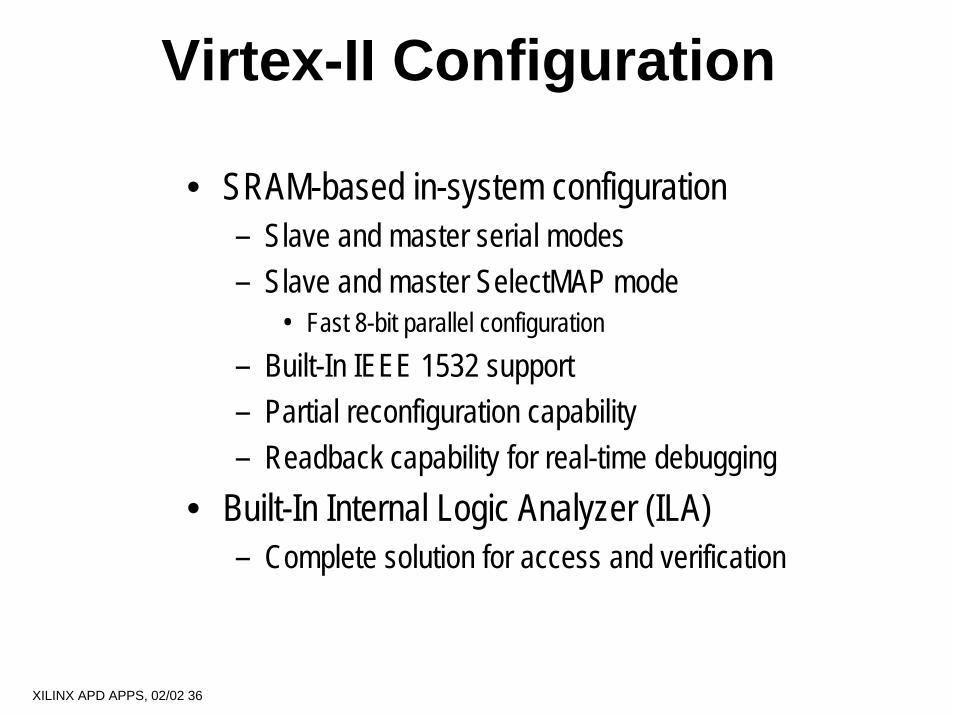
Virtex-II Configuration
• SRAM-based in-system configuration– Slave and master serial modes– Slave and master SelectMAP mode
• Fast 8-bit parallel configuration– Built-In IEEE 1532 support– Partial reconfiguration capability– Readback capability for real-time debugging
• Built-In Internal Logic Analyzer (ILA)– Complete solution for access and verification
XILINX APD APPS, 02/02 36
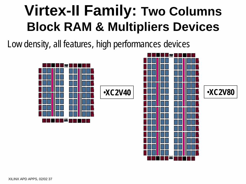
Virtex-II Family: Two Columns Block RAM & Multipliers Devices
•XC2V40 •XC2V80
Low density, all features, high performances devices
XILINX APD APPS, 02/02 37
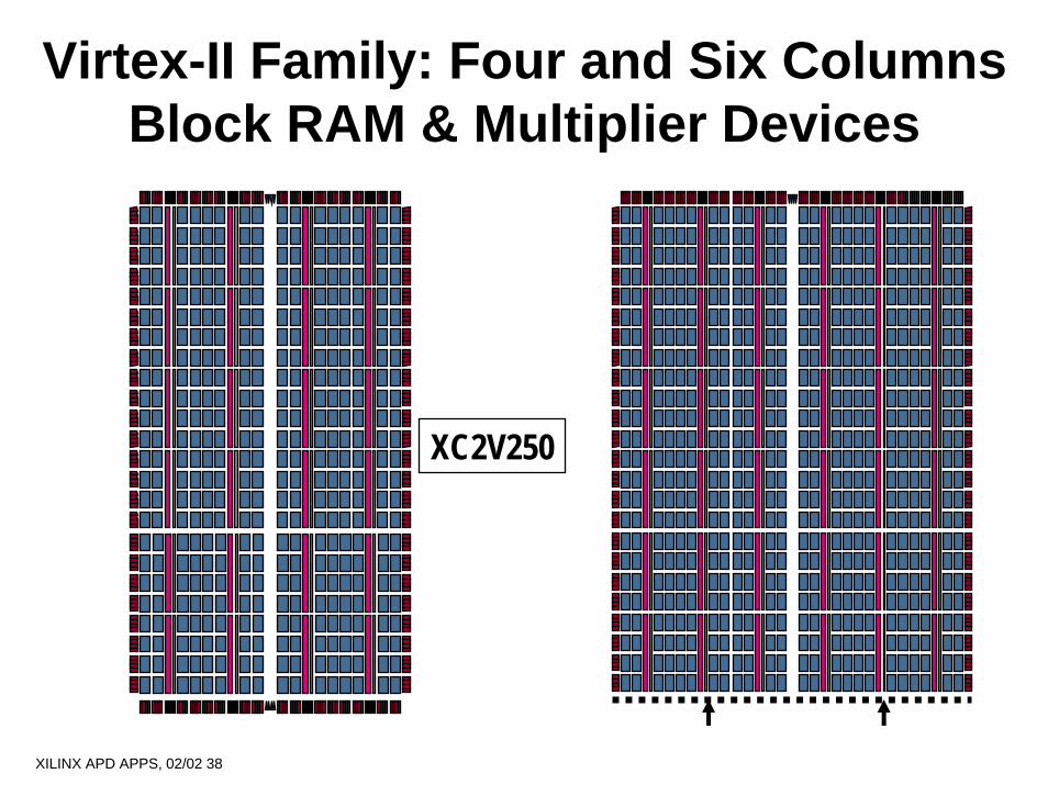
Virtex-II Family: Four and Six Columns Block RAM & Multiplier Devices
XC2V250
XILINX APD APPS, 02/02 38
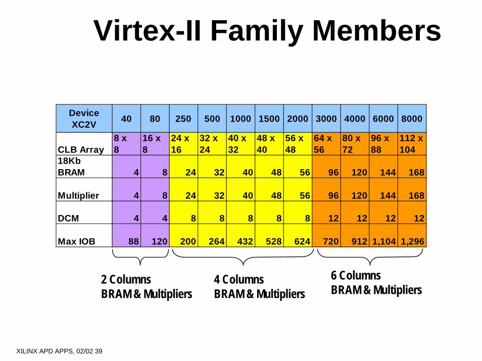
Virtex-II Family Members
Device XC2V 40 80 250 500 1000 1500 2000 3000 4000 6000 8000
CLB Array8 x 8
16 x 8
24 x 16
32 x 24
40 x 32
48 x 40
56 x 48
64 x 56
80 x 72
96 x 88
112 x 104
18Kb BRAM 4 8 24 32 40 48 56 96 120 144 168
Multiplier 4 8 24 32 40 48 56 96 120 144 168
DCM 4 4 8 8 8 8 8 12 12 12 12
Max IOB 88 120 200 264 432 528 624 720 912 1,104 1,296
6 Columns BRAM & Multipliers
2 Columns BRAM & Multipliers
4 Columns BRAM & Multipliers
XILINX APD APPS, 02/02 39
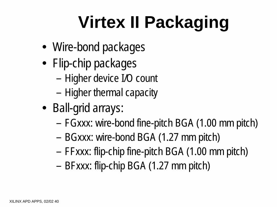
Virtex II Packaging• Wire-bond packages• Flip-chip packages
– Higher device I/O count– Higher thermal capacity
• Ball-grid arrays:– FGxxx: wire-bond fine-pitch BGA (1.00 mm pitch)– BGxxx: wire-bond BGA (1.27 mm pitch)– FFxxx: flip-chip fine-pitch BGA (1.00 mm pitch)– BFxxx: flip-chip BGA (1.27 mm pitch)
XILINX APD APPS, 02/02 40
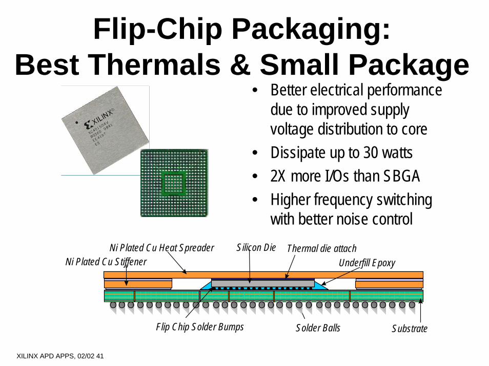
Flip-Chip Packaging:Best Thermals & Small Package
• Better electrical performance due to improved supply voltage distribution to core
• Dissipate up to 30 watts• 2X more I/Os than SBGA• Higher frequency switching
with better noise controlThermal die attach
Underfill Epoxy
Flip Chip Solder Bumps Solder Balls
Ni Plated Cu Heat Spreader Silicon Die
Substrate
Ni Plated Cu Stiffener
XILINX APD APPS, 02/02 41

Virtex-II PackagingDevice XC2V 40 80 250 500 1000 1500 2000 3000 4000 6000 8000
Max user I/Os 88 120 200 264 432 528 624 720 912 1,104(1296) 1108
CS144 88 92 92FG256 88 120 172 172 172FG456 200 264 324FG676 392 456 484FF896 432 528 624FF1152 720 824 824 824FF1517 912 1,104 1,108BG575 328 392 408BG728 456 516BF957 624 684 684 684 684
• FF and BF are flip-chip ball grid arrays packages• Pinout compatibility inside same color rectangle
XILINX APD APPS, 02/02 42
Agenda:
•VirtexTM-II Overview•Virtex-II Design Solutions•Conclusion
XILINX APD APPS, 02/02 43
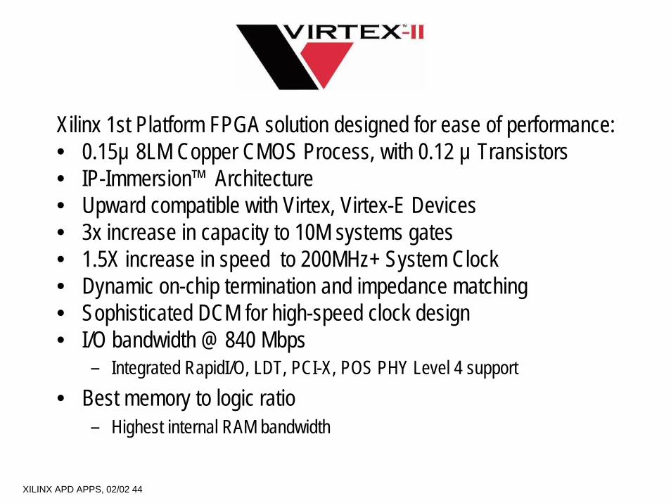
Xilinx 1st Platform FPGA solution designed for ease of performance:• 0.15µ 8LM Copper CMOS Process, with 0.12 µ Transistors• IP-Immersion™ Architecture• Upward compatible with Virtex, Virtex-E Devices• 3x increase in capacity to 10M systems gates• 1.5X increase in speed to 200MHz+ System Clock• Dynamic on-chip termination and impedance matching• Sophisticated DCM for high-speed clock design• I/O bandwidth @ 840 Mbps
– Integrated RapidI/O, LDT, PCI-X, POS PHY Level 4 support• Best memory to logic ratio
– Highest internal RAM bandwidth
XILINX APD APPS, 02/02 44