· web viewelectrical quantities from mechanical0.1 quantities. resistance and ohm's...
TRANSCRIPT
ELECTRONICS FOR NON-ENGINEERS===================================================================
Electrical Fundamentals. Chapter 0
Electrical Quantities From Mechanical 0.1 Quantities. Resistance and Ohm's Law. 0.2 Series Circuits and Kirchhoff's Voltage Law. 0.3 Parallel Circuits and Kirchhoff's Current Law. 0.4 Prefixes. 0.5 Numerical 0.6 Examples. Capacitance. 0.7 Inductance. 0.8 0.9 Problems.0.10 Answers to Problems.
Chapter 0.Electrical Fundamentals.
This chapter is intended as a review of material which the student should be familiar with. If the student is not familiar with the material in this chapter, intensive study of this chapter may not be sufficient. A review of textbooks used in previous courses may be required.
0.1 Electrical Quantities From Mechanical Quantities.
Electric Charge.
It is difficult to say exactly what electric charge is but you are all familiar with it. You walk across the carpet on a cold winter morning, reach for the doorknob and - ZAP - you get an electric shock. Your body acquired the property of electric charge by friction with the carpet.
Electric charge can be placed on objects under somewhat more controlled circumstances. One way is to rub a rubber rod with a piece of cat's fur. The rod will now attract small objects such as bits of paper. The charge on the rod induces the opposite charge on the bits of paper. The fur will also attract small objects but it is not as easy to handle as the rod.
The property of electric charge will cause two bodies which possess a charge to exert a force on one another. The magnitude of this force is directly proportional to the amount of charge on each body and inversely proportional to the square of the distance between the two bodies. In equation form this law is
F = q1 q2 / r2 (0.1)
where F is the force in Newtons, q1 is the amount of charge on body 1, q2 is the amount of charge on body 2 and r is the distance between the two bodies in meters.
If the distance is 1 meter and the force is 1 Newton and the two bodies have the same amount of charge, the amount of charge on each body is 1 coulomb. This is the definition of a coulomb, which is the unit of charge in the MKS system.
If the two bodies have charges of the same sign, the force is repulsive. If the two bodies have charges of opposite sign, the force is attractive.
The charge on one electron is 1.601864 x 10⁻¹⁹ coulombs. Therefore, one coulomb of charge is equal to the total charge of 6.24 x 10¹⁸ electrons.
In terms of mechanical units the dimensions of a coulomb are
Coulombs = Meters x Newtons1/2 (0.2)
Electric Current.
Electric current is the motion of electric charge through any conducting material. When a direct current is flowing in a wire, electrons are in continuous unidirectional motion along the wire.
Current expresses the amount of charge per unit time passing a given point on a conductor. One way of defining current would be to specify the number of electrons per second passing a point. Although this would be a perfectly valid way of specifying the amount of current in a conductor, the numbers which would result in practical applications would be so large as to be unwieldy. More practical numbers result if the coulomb is taken as the basic unit of charge instead of the electron.
The most commonly used unit of current is the ampere. One ampere is equal to one coulomb of charge per second passing a point on a conductor. Thus the basic units of current are
(0.3) Amperes = Coulombs / seconds
If desired the mechanical units of charge could be substituted into this equation and a strictly mechanical definition of current could be obtained. This is left as an exercise at the end of this chapter.
The symbol I is used for steady-state currents while the symbol i is used for time-varying currents.
The mathematical equations which relate current, charge and time are
(0.4) I = Q / t
or
(0.5) I = dq / dt
The use of an upper-case letter for steady-state values and the lower-case equivalent for time-varying values is common practice in electricity and magnetism.
Conventional Current.
When an electric current moves through a circuit, the negatively charged electrons flow toward the positively charged part of the circuit. This means that electrons come out of the - side of a battery and go into the + side.
Physicists and electrical engineers alike prefer to use conventional current instead of electron current. Conventional current does what you would expect it to do. It flows out of the + side of a battery and flows into the - side.
Some students find this confusing. If you are among the confused, try this. Never think about electron current. Banish electron current forever from your mind and think only in terms of conventional current.
If any one man can be blamed for this confusion it seems to be the fault of Benjamin Franklin. Everyone knows about his "kite in the lightning storm" experiment. What few people know is that Dr. Franklin wrote one of the first if not the first textbook on electricity. He assembled all that was known at that time about electricity and put it in one book. He seems to have added very little in the way of original work himself but one thing he did add was a sign convention for electric charge. The convention he chose was a guess and he guessed wrong. Just think of it, if he had guessed the other way, we would have positive electrons and conventional current would be the same as electron current.
Electrical Potential.
Mechanical potential is expressed in units of work- energy. Electrical potential also is an expression of work which can be done or energy stored. The units are work per unit charge. If work is done on a given amount of charge, the potential has increased. If the charge does work the potential has decreased.
Electrical potential like mechanical potential has no absolute zero. Electrical potential is always expressed as a potential difference between two points. In some cases one of the
points is implied or understood in context. Electrical potential is meaningless unless two points are specified, implied, or understood.
Because potential is specified between two points the term potential difference is often used. The "difference" is usually omitted when speaking and often omitted when writing; "potential difference" is always understood by speaker, listener, writer and reader.
The unit of electrical potential difference is the volt. Potential difference is often called the voltage difference or the voltage drop but most often just the voltage.
If one joule of work is done on one coulomb of charge, the charge is moved through a potential difference of positive one volt. If one coulomb of charge does one joule of work, the charge has moved through a potential difference of minus one volt.
The basic units of voltage difference are
(0.6) volts = joules / coulomb
As with units of current, the mechanical units of charge could be substituted into equation 0.6 to obtain purely mechanical units of voltage difference.
The term "electromotive force" was once regularly used to describe electrical potential difference. This led to the use of the symbol emf and later to the letter E to symbolize potential difference. In more recent times the letter V has been adopted for drops across passive components. The letter E will be used for the voltage of energy sources. This convention will be used throughout this book. The equations for voltage in terms of more basic units are
(0.7) V = W / Q
or
(0.8) dv / dt = dw/dt / Q
Charge is not indicated as being time-varying because it is conserved. Charge can neither be created nor destroyed.
Electrical Power.
In mechanics, power is the rate of doing work or work per unit time. (0.9) Power = work / Time
Electrical power is no different. Electric power is
(0.10) Power = Current x Voltage.
If we substitute the mechanical units of voltage and current into equation 0.10 we have
(0.11) Watts = Coulombs / Second x Joules / Coulomb = Joules / Second
Thus
(0.12) P = I x V
0.2 Resistance and Ohm's Law.
An Electric Circuit.
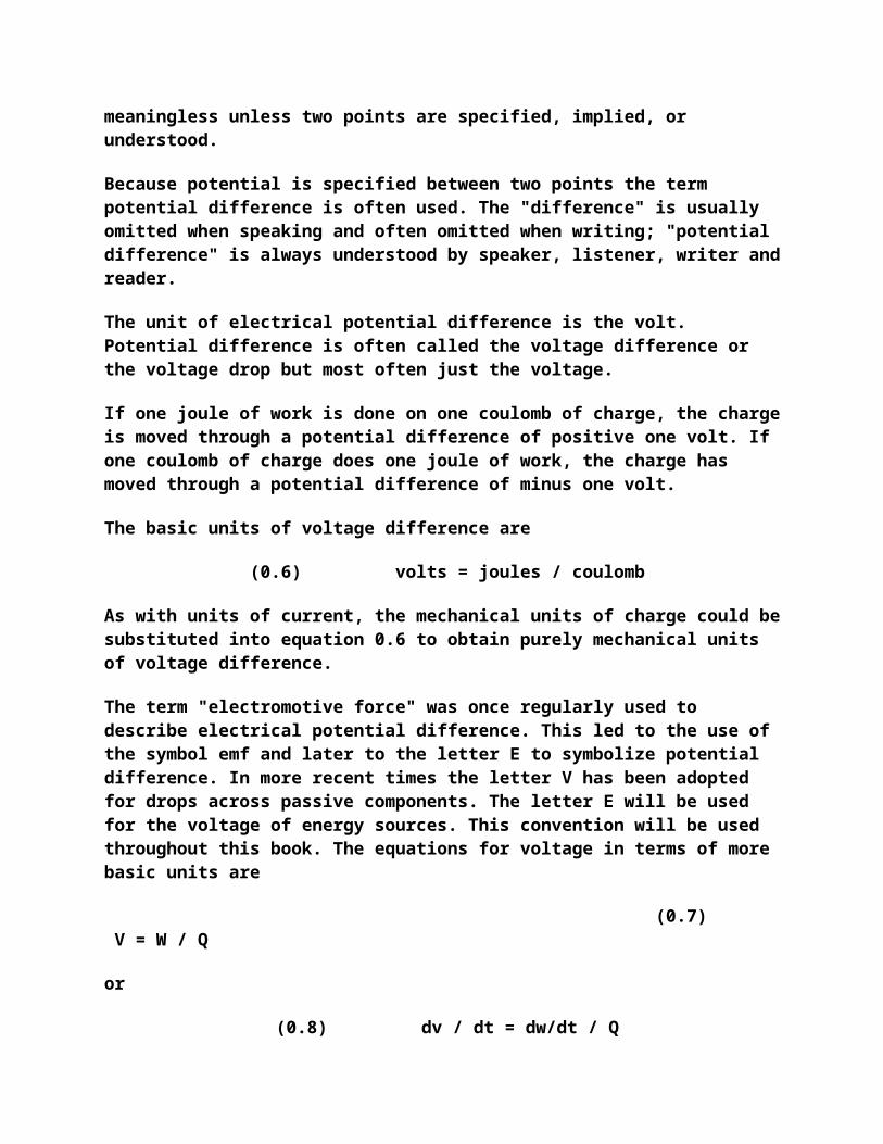
In order for electricity to be useful, it must be harnessed to do work for us. The usual way of making electricity do work is to connect a source of electric energy to a device which converts the electric energy into another useful form of energy. An example of this is the flashlight, the schematic diagram of which is shown in figure 0.1.
Figure 0.1 Schematic Diagram of a Flashlight.
For a verbal description click here.
The battery on the left converts chemical energy into electrical energy. The lamp on the right converts the electrical energy into electromagnetic energy, some of which is in the visible light part of the electromagnetic spectrum. The switch is used to interrupt the flow of electrons and permit the light to be turned on and off. The lines on the drawing indicate conductors such as wire which normally have negligible amounts of resistance compared to the rest of the circuit.
Resistance.
When an electric current flows through a very good conductor, such as a copper wire, the electrons move very easily and very little work is required to move them. A copper wire has very low, almost zero resistance.
When an electric current attempts to flow through a very poor conductor, such as a piece of glass or the open switch, a near infinite amount of energy would be required. In purely practical terms, electrons do not move through pieces of glass or open switches and there is no current flow. No current flow means that no charge is moved and no work is done. A piece of glass or an open switch has very high, almost infinite resistance.
When an electric current flows through a thin wire such as the filament in the lamp, the electrons can be moved but considerable work is required to make the electrons move. The filament of a lamp and other devices on which electricity does work are said to have finite resistance.
Current, Work and Potential.
If the current flows through a part of the circuit which has zero resistance (a super conductor) no work is required to move the electrons through this part of the circuit. Electric charge is being moved but no work is being done. In as much as potential difference (voltage) is defined as work per unit charge (equation 0.6) if the work is zero, the voltage is zero.
If the current flows through a part of the circuit which has a finite resistance, work is required to move the charge. If work is done, there is a potential difference across that part of the circuit. If the amount of charge per unit time remains constant, doubling of the amount of resistance will cause the amount of work to be doubled and the voltage to be doubled. Therefore, the voltage is directly proportional to the resistance.
If we now hold the resistance constant and allow the current (charge per unit time) to vary we discover the following. If the current doubles, there is twice as much charge to be moved and twice as much work will be required to move it. Which leads us to the conclusion that the voltage is directly proportional to the current.
We have now concluded that the voltage is directly proportional to the current and the resistance. As we saw at the beginning of this discussion, if the resistance is zero, the voltage is zero. On the other hand if the resistance is finite and the current is zero, there are no charges to do work on and there can be no potential difference. This is a strong indication that voltage is proportional to the product of resistance and current.
(0.13) V = I x R
Resistance is defined in terms of volts and amps as follows. If a current of 1 ampere is flowing through a resistance of 1 ohm, the voltage which results will be 1 volt. Even the ohm can be defined in terms of purely mechanical units.
The above discussion is as close as we can come to a derivation of Ohm's law (equation 0.13). In fact Ohm's law was discovered experimentally and is strictly an empirical law.
Resistance and Power.
It is important to know how much power is being dissipated in a resistor. Every resistor has a maximum power rating. If this power is exceeded, the resistor will get overheated and quite literally burn up. Whenever a resistor is put into service a power calculation should be performed to make sure that the resistor will not burn out.
One way to make a power calculation is to multiply the current through the resistor by the voltage across it. This must be valid but if you know only one, voltage or current, you must use Ohm's law to calculate the other. A couple of shortcuts can be developed by combining equation 0.12 (power) with equation 0.13 (Ohm's law). A direct substitution of 0.12 into 0.11 gives
P = I x I x R = I2 (0.14) x R
Solving Ohm's law for current and substitution gives
P = (V / R) x V = V2 (0.15) / R
These equations should not be confused with the definition of power but they are often very handy.
0.3 Series Circuits and Kirchhoff's Voltage Law.
Electric circuits get much more complex than the flashlight shown in Figure 0.1. We will work our way up from simple circuits to more complex circuits.
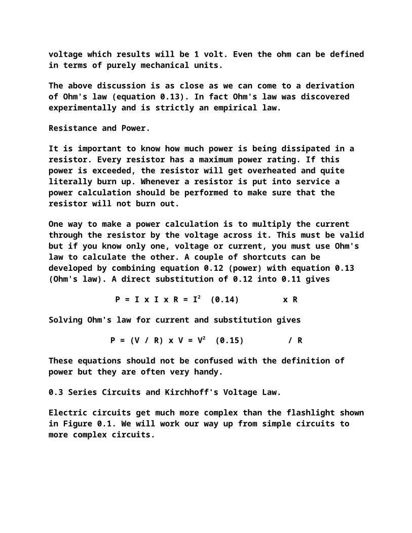
Figure 0.2 Schematic Diagram of a Series Circuit.
For a verbal description click here.
A series circuit is defined as a circuit in which there is only one path to be followed from a given point, around the circuit and back to the same point. Figure 0.2 qualifies under this definition of a series circuit.
In Figure 0.2 the letter E is used to symbolize the emf or potential difference across the battery. The symbol V1 is used for the potential difference across the resistor R1. In general the symbol VN will be used for the potential across any resistor RN.
Conventional current flows out of the positive terminal of the battery, through R1, through R2, through R3 and to the negative terminal of the battery. Current is symbolized by the letter I.
Current in Series Circuits.
Let us use the general symbol IN for the current in resistor RN and the letter I for the current in the battery. Remember that current could be expressed as the number of electrons per second passing a point in the circuit.
As electrons move around the circuit, there are no side roads for them to take. Electrons cannot pile up at any particular place in the circuit. If there was a pile-up, the concentration of negative charge would repel additional electrons from that vicinity and the pile-up would soon be gone. Pile-ups never happen in the first place.
Because we have established that electrons cannot accumulate at any point or get out of the circuit at any point, we may say that the number of electrons per second passing any point in the circuit of Figure 0.2 is the same as the number of electrons per second passing any other point in the circuit. In other words the current at any point in the circuit is exactly the same as the current at any other point in the circuit. This can be stated in equation form as
I = I1 = I2 = I3 (0.16)
Equation 0.16 is a consequence of Kirchhoff's current law although we don't officially know that yet.
Voltage in Series Circuits.
Remember that potential difference or voltage is work per unit charge. From mechanics remember: 1) the equivalents of work and energy, 2) the conservation of energy and 3) the conservation of charge. Also remember that the current in any resistor in Figure 0.2 is the same as the current in any other resistor and the same as the current in the battery.
The amount of work done by the battery is equal to the sum of the work done on each resistor, In equation form
W = W1 + W2 + W3 (0.17)
If we solve equation 0.7 for W and substitute into equation 0.17 we have
QE = QV1 + QV2 + QV3 (0.18)
As the current is the same everywhere in the circuit, the charge per unit time is the same and all occurrences of charge are the same. The charge Q will cancel out. Thus we have
E = V1 + V2 + V3 (0.19)
Equation 0.19 is a special case of Kirchhoff's voltage law.
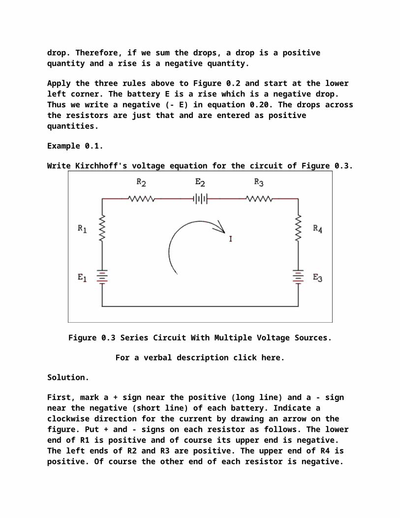
Kirchhoff's voltage law states that the algebraic sum of all voltage drops around any closed loop is equal to zero. Thus, Kirchhoff's voltage equation for the circuit of Figure 0.2 is
- E + V1 + V2 + V3 (0.20) = 0
Voltage Rises and Drops.
All voltages are really voltage differences. A potential difference or voltage difference can be either a voltage rise or a voltage drop. Although it may be stating the obvious, a rise is an increase in potential or voltage and a drop or fall is a decrease in potential or voltage. If we start at a particular point in a circuit and move around the circuit we may move from a point of low potential to a point of higher potential. We have traversed a potential rise. If we move from a point of high potential to a point of higher potential we have again traversed a potential rise. The starting point makes no difference; it is the change that is important. Similarly if we move from a point of any given potential to a point of lower potential we have traversed a potential drop or fall.
For example, if we traverse the battery in Figure 0.2 from bottom to top, we have traversed a rise. Conversely if we traverse the battery from top to bottom, we have traversed a drop. From this you can see that a battery is not automatically a potential rise; it depends on the direction of travel.
It is easy to tell the direction of the potential or polarity of a battery because of the polarity markings. A battery will always have the same polarity (positive on the long line) regardless of whether it is being charged (current flowing into the positive terminal) or discharged (current flowing out of the positive terminal). The positive terminal of the battery is always positive no matter which way the current is flowing.
Resistors and other passive devices are another story. Conventional current always flows out of the most negative end of a passive device. Thus, the end where the current goes in is more positive than the end where the current comes out.
In solving Kirchhoff's equation it is very important to give the proper sign to each quantity. If an incorrect sign is given to a particular value, the result will be incorrect. Here are some rules to follow in writing Kirchhoff's equations.
1. 1 Mark the polarity on all voltage sources (batteries) by placing a minus (-) sign next to the negative terminal (short line) and a plus (+) sign next to the positive terminal (long line).
2. 2 Assume a direction for the current. Clockwise is a standard assumption used by those who solve circuit equations. Don't be concerned if you can't tell which direction the current is actually flowing. The numeric answer will have a sign which will tell us if the initial assumption was right or wrong.
3. 3 Mark the polarity on all passive devices (resistors) by placing a plus (+) sign at the end where the current enters and a minus (-) sign at the end where the current exits.
Now that you have polarity markings on each part in the circuit you are almost ready to write a Kirchhoff's equation.
Do not be concerned about the fact that there are + and - signs next to each other on opposite ends of the same wire. The signs refer to that particular circuit element alone. The positive end is more positive than the negative and the negative end is more negative than the positive end. The signs say nothing about what the potential is with respect to other parts of the circuit.
Kirchhoff's law states that the sum of all voltage drops is equal to zero. It could just as well say that the sum of all voltage rises is equal to zero. The only difference between the two resulting equations will be that one has been multiplied through by -1 as compared to the other.
If you are summing the rises, a drop is a negative rise. A drop is the negative of a rise. Conversely a rise is the negative of a drop. Therefore, if we sum the drops, a drop is a positive quantity and a rise is a negative quantity.
Apply the three rules above to Figure 0.2 and start at the lower left corner. The battery E is a rise which is a negative drop. Thus we write a negative (- E) in equation 0.20. The drops across the resistors are just that and are entered as positive quantities.
Example 0.1.
Write Kirchhoff's voltage equation for the circuit of Figure 0.3.
Figure 0.3 Series Circuit With Multiple Voltage Sources.
For a verbal description click here.
Solution.
First, mark a + sign near the positive (long line) and a - sign near the negative (short line) of each battery. Indicate a clockwise direction for the current by drawing an arrow on the figure. Put + and - signs on each resistor as follows. The lower end of R1 is positive and of course its upper end is negative. The left ends of R2 and R3 are positive. The upper end of R4 is positive. Of course the other end of each resistor is negative. Now we can write the equation. Start at the lower left corner and move around the circuit in a clockwise direction. If we sum the drops we get
- E1 + V1 + V2 - E2 + V3 + V4 + E3 (0.21) = 0
If we sum the voltage rises we get
E1 - V1 - V2 + E2 - V3 - V4 - E3 (0.22) = 0
Equation 0.22 is just equation 0.21 multiplied by -1. If we were to plug in numbers and solve them, both would give the same answer.
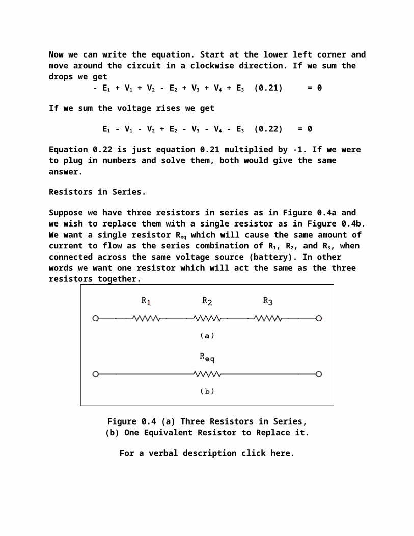
Resistors in Series.
Suppose we have three resistors in series as in Figure 0.4a and we wish to replace them with a single resistor as in Figure 0.4b. We want a single resistor Req which will cause the same amount of current to flow as the series combination of R1, R2, and R3, when connected
across the same voltage source (battery). In other words we want one resistor which will act the same as the three resistors together.
Figure 0.4 (a) Three Resistors in Series,(b) One Equivalent Resistor to Replace it.
For a verbal description click here.
We now apply a voltage E to the resistors as shown in Figure 0.5. Kirchhoff's equation is - E + V1 + V2 + V3 = 0. Solving for E gives
E = V1 + V2 + V3 (0.23)
The equivalent resistor Req would give the simple equation
E = Veq (0.24)
If we substitute Ohm's law VN = I x RN and remember that the current I is the same everywhere in a series circuit we have
I x Req = I x R1 + I x R2 + I x R3 (0.25)
canceling I
Req = R1 + R2 + R3 (0.26)
and in the general form
Req = R1 + R2 + ... + RN (0.27)
Equation 0.27 says that the equivalent of any number of resistors in series is the sum of all of the resistors in series.
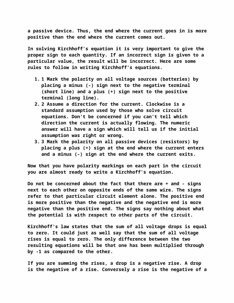
Figure 0.5 (a) Three Series Resistors Connected to a VoltageSource, (b) One Equivalent Resistor Connected to a
Similar Voltage Source.
For a verbal description click here.
Logical Checks.
In any problem-solving course it is a good idea to have in mind some rules of logic for checking answers. You should look at an answer and ask yourself "Does that answer make sense?" From time to time this book will give some common sense rules under the heading of "Logical Checks".
When finding the equivalent of series resistors the equivalent will always be greater than the largest single resistor.
0.4 Parallel Circuits and Kirchhoff's Current Law.
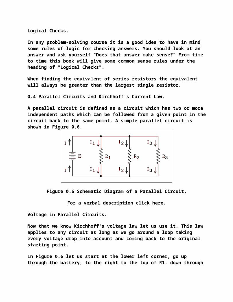
A parallel circuit is defined as a circuit which has two or more independent paths which can be followed from a given point in the circuit back to the same point. A simple parallel circuit is shown in Figure 0.6.
Figure 0.6 Schematic Diagram of a Parallel Circuit.
For a verbal description click here.
Voltage in Parallel Circuits.
Now that we know Kirchhoff's voltage law let us use it. This law applies to any circuit as long as we go around a loop taking every voltage drop into account and coming back to the original starting point.
In Figure 0.6 let us start at the lower left corner, go up through the battery, to the right to the top of R1, down through R1 and then back to the left to the starting point. The resulting equation is -E + V1 = 0 or E = V1.
Now let us follow a path through R2. Start at the lower left corner, go up through the battery, to the right to the top of R2, down through R2 and then back to the left to the starting point. The resulting equation is -E + V2 = 0 or E = V2.
The argument is the same for R3. Thus we have shown that
E = V1 = V2 = V3 (0.28)
In a simple parallel circuit the voltage across any one element is the same as the voltage across any other element in the same circuit.
Current in Parallel Circuits.
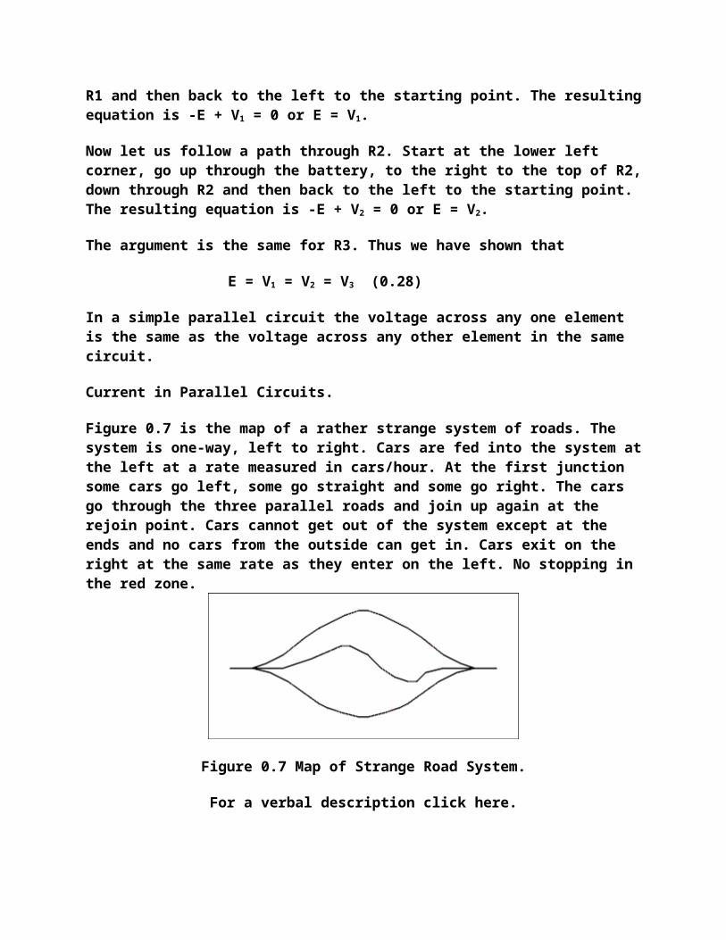
Figure 0.7 is the map of a rather strange system of roads. The system is one-way, left to right. Cars are fed into the system at the left at a rate measured in cars/hour. At the first junction some cars go left, some go straight and some go right. The cars go through the three parallel roads and join up again at the rejoin point. Cars cannot get out of the system except at the ends and no cars from the outside can get in. Cars exit on the right at the same rate as they enter on the left. No stopping in the red zone.
Figure 0.7 Map of Strange Road System.
For a verbal description click here.
When the car-current (cars/hour) splits it is obvious that the sum of the car-currents (KN) in the three paths is equal to the car-current (K) in the main path.
K = K1 + K2 + K3 (0.29)
Look at Figure 0.6 and visualize the electrons in the circuit doing the same as the cars on the road. This is the justification for writing the equation
I = I1 + I2 + I3 (0.30)
which is a special case of Kirchhoff's current law.
Kirchhoff's current law says that the sum of all currents flowing into a junction is equal to zero. If current going in is defined as positive, then current coming out is negative.
In Figure 0.6 the top line is a junction where currents may be summed and the bottom line is another junction where currents may be summed. If we sum the currents in the top line we have
I - I1 - I2 - I3 (0.31) = 0
if we sum the currents in the bottom junction we have
- I + I1 + I2 + I3 (0.32) = 0
The only difference between equations 0.25 and 0.26 is that one is the negative of the other. Numerical solution of both equations will give the same answer.
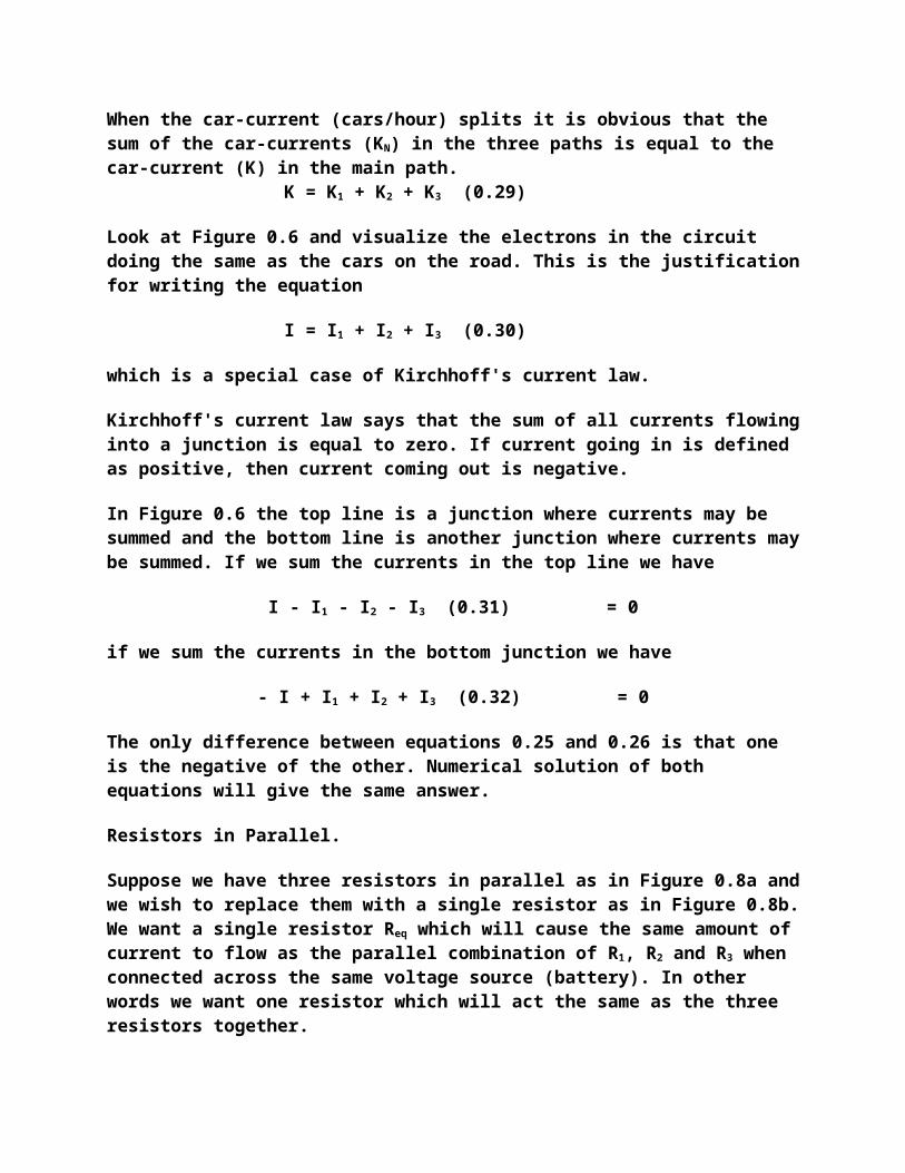
Resistors in Parallel.
Suppose we have three resistors in parallel as in Figure 0.8a and we wish to replace them with a single resistor as in Figure 0.8b. We want a single resistor Req which will cause the same amount of current to flow as the parallel combination of R1, R2 and R3 when connected across the same voltage source (battery). In other words we want one resistor which will act the same as the three resistors together.
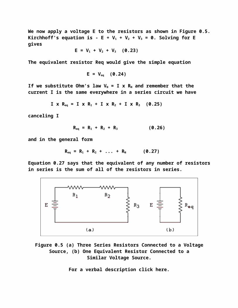
Figure 0.8 (a) Three Resistors in Parallel,(b) One Equivalent Resistor to Replace it.
For a verbal description click here.
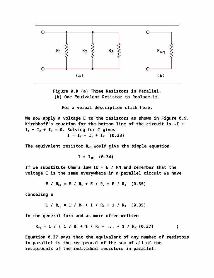
We now apply a voltage E to the resistors as shown in Figure 0.9. Kirchhoff's equation for the bottom line of the circuit is -I + I1 + I2 + I3 = 0. Solving for I gives
I = I1 + I2 + I3 (0.33)
The equivalent resistor Req would give the simple equation
I = Ieq (0.34)
If we substitute Ohm's law IN = E / RN and remember that the voltage E is the same everywhere in a parallel circuit we have
E / Req = E / R1 + E / R2 + E / R3 (0.35)
canceling E
1 / Req = 1 / R1 + 1 / R2 + 1 / R3 (0.35)
in the general form and as more often written
Req = 1 / ( 1 / R1 + 1 / R2 + ... + 1 / RN (0.37) )
Equation 0.37 says that the equivalent of any number of resistors in parallel is the reciprocal of the sum of all of the reciprocals of the individual resistors in parallel.
Figure 0.9 (a) Three Paralleled Resistors Connected to aVoltage Source, (b) One Equivalent Resistor
Connected to a Similar Voltage Source
For a verbal description click here.
Logical Checks.
When finding the equivalent of parallel resistors the equivalent will always be less than the smallest single resistor.
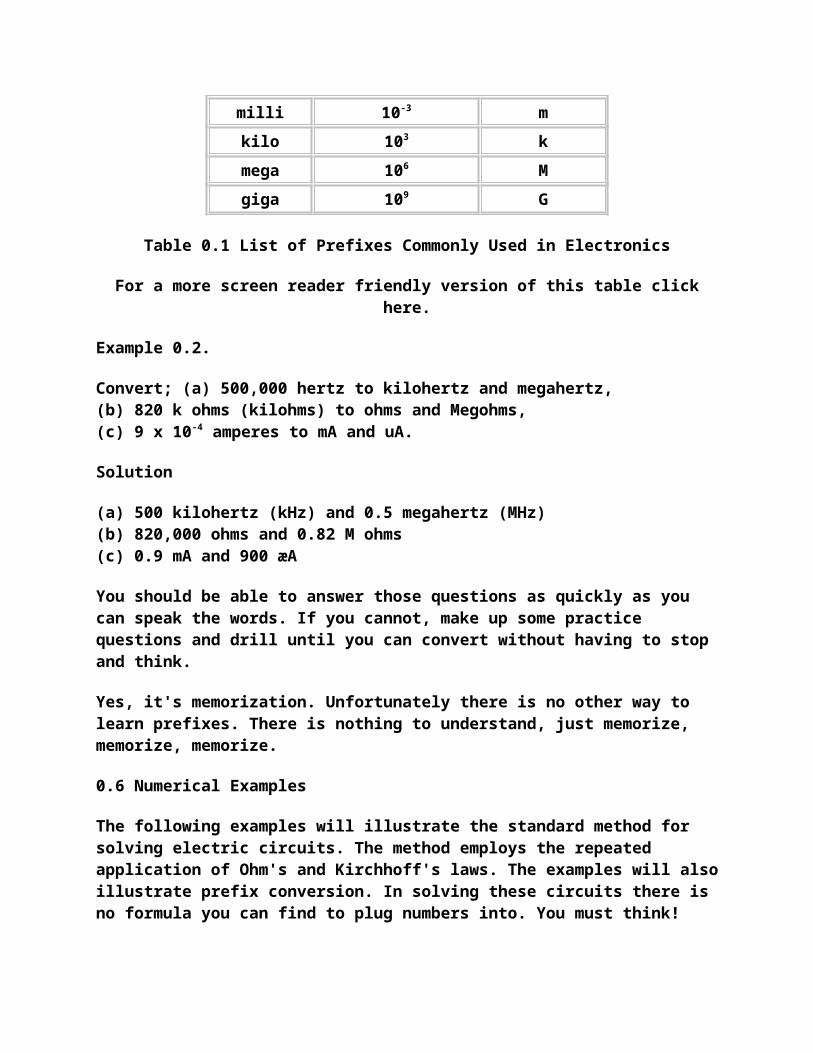
0.5 Prefixes.
Prefixes are used throughout the sciences to indicate multiplication by a power of ten. You probably already know that 1 centimeter = 10-2 meters and 1 kilogram = 103 grams.
In electricity and magnetism the values are so large or so small as to require the use of prefixes. You MUST be able to make instant conversions in your head from one prefix to another or the unprefixed unit. Here are the prefixes you should know.
For a more screen reader friendly version of the table below click here. Prefix Multiplier Symbol pico 10-12 p nano 10-9 n micro 10-6 u milli 10-3 m kilo 103 k
mega 106 M giga 109 G
Table 0.1 List of Prefixes Commonly Used in Electronics
For a more screen reader friendly version of this table click here.
Example 0.2.
Convert; (a) 500,000 hertz to kilohertz and megahertz,(b) 820 k ohms (kilohms) to ohms and Megohms,(c) 9 x 10⁻⁴ amperes to mA and uA.
Solution
(a) 500 kilohertz (kHz) and 0.5 megahertz (MHz)(b) 820,000 ohms and 0.82 M ohms(c) 0.9 mA and 900 æA
You should be able to answer those questions as quickly as you can speak the words. If you cannot, make up some practice questions and drill until you can convert without having to stop and think.
Yes, it's memorization. Unfortunately there is no other way to learn prefixes. There is nothing to understand, just memorize, memorize, memorize.
0.6 Numerical Examples
The following examples will illustrate the standard method for solving electric circuits. The method employs the repeated application of Ohm's and Kirchhoff's laws. The examples will also illustrate prefix conversion. In solving these circuits there is no formula you can find to plug numbers into. You must think!
Example 0.3.
In the circuit of Figure 0.2 the battery voltage E is 24.00 volts. R1 = 470 ohms, R2 = 220 ohms and R3 = 330 ohms. What is the current drawn from the battery?
Solution:
The equivalent resistance in the circuit is R1 + R2 + R3 = 470 ohms + 220 ohms + 330 ohms = 1020 ohms. The current drawn from the battery is I = E / Req I = 24 v / 1020 ohms = 2.35 x 10⁻² A = 23.5 mA.
Example 0.4.
In the circuit of Figure 0.2 the resistance of each resistor is as follows. R1 = 910 ohms, R2 = 1.1 k ohms and R3 = 1.3 k ohms. The voltage across R2 is 4.985 volts. What is the battery voltage?
Solution:
Intermediate results should always be carried out to four significant digits. Answers should be rounded off to three significant digits. The current in R2 is I2 = V2 / R2 = 4.985 v / 1.1 k ohms = 4.532 mA. This also is the current in R1 and R3, I = I1 = I2 = I3. The voltage across R1
is V1 = I1 x R1 = 4.532 mA x 910 ohms = 4.124 v, V2 is given and V3 = 5.892 v. The battery voltage E is equal to the sum of all resistor voltages E = 4.124 v + 4.985 v + 5.892 v = 15.001 v. Rounding off, the battery voltage E = 15.0 volts.
Example 0.5.
In the circuit of Figure 0.6 the resistance of R2 is 620 ohms and the current through it is 125 mA. The resistance of R3 is 15 k ohms. What is the current through R3?
Solution:
The voltage across R2 is V2 = I2 x R2 = 125 mA x 620 ohms = 77.50 v. In a parallel circuit E = V1 = V2 = V3; hence V3 = 77.50 v. I3 = V3 / R3 = 77.50 v / 15 k ohms = 5.17 mA.
Example 0.6.
In figure 0.6 the current in R1 is 66.6 mA, the current in R2 is 39.4 mA, the power in R3 is 1.7 watts and the resistance of R3 is 820 ohms. What is the total battery current?
Solution:
The current in R3 is I3 = (P / R)1/2 I3 = (1.7 w / 820 ohms)1/2 = 4.553 x 10⁻² A = 45.53 mA. The battery current I = I1 + I2 +I3 I = 66.6 mA + 39.4 mA + 45.53 mA = 152 mA.
0.7 Capacitance.
A capacitor is a device which has the property of capacitance. Capacitance is the property possessed by a capacitor. Eh?
A capacitor is nothing more than an open circuit. Yet it is the most useful open circuit ever discovered. A capacitor consists of two conductors separated by an insulator. Capacitors can best be described as devices which permit electric charge to be stored and released in a controllable and repeatable manner.
Capacitance is that electrical property which resists changes in the voltage across the circuit containing the capacitance.
Capacitors are devices in which energy can be stored for short periods of time. The energy is stored in the electric field between the two conductors of the capacitor.
Capacitance is defined as
(0.38) C = Q / V
where C is called the capacitance and is measured in farads, Q is the charge on either conductor in coulombs and V is the potential difference between the two conductors in volts.
If equation 0.38 is solved for charge we have
(0.39) Q = C V
If we take the time derivative of both sides of this equation we have
(0.40) dq / dt = C dv / dt
But dq/dt = i; therefore,
(0.41) i = C dv / dt
This equation turns out to be much more useful than you might imagine.
Example 0.7.
If the current through a capacitor is 120 milliamperes and the rate of change of voltage is to be 1.5 volts/milliseconds, what is the capacitance?
Solution:
Solving equation 0.41 for C gives
C = I / (dv/dt) = 120 x 10-3 / (1.5 v / 10-3) = 8.0 x 10⁻⁵ farads.
8 x 10⁻⁵ farads may be expressed as 80 microfarads or 80 uf. Both answers are correct, they are just different ways of expressing the same number.
Equation 0.41 tells us that we cannot change the voltage across a capacitor in zero time. If we tried, the current would be infinite. This equation also tells us that if we maintain a constant current through a capacitor, the voltage across it will change linearly with time. This is the basis of the linear sweep in an oscilloscope.
Resistance-Capacitance Circuit.
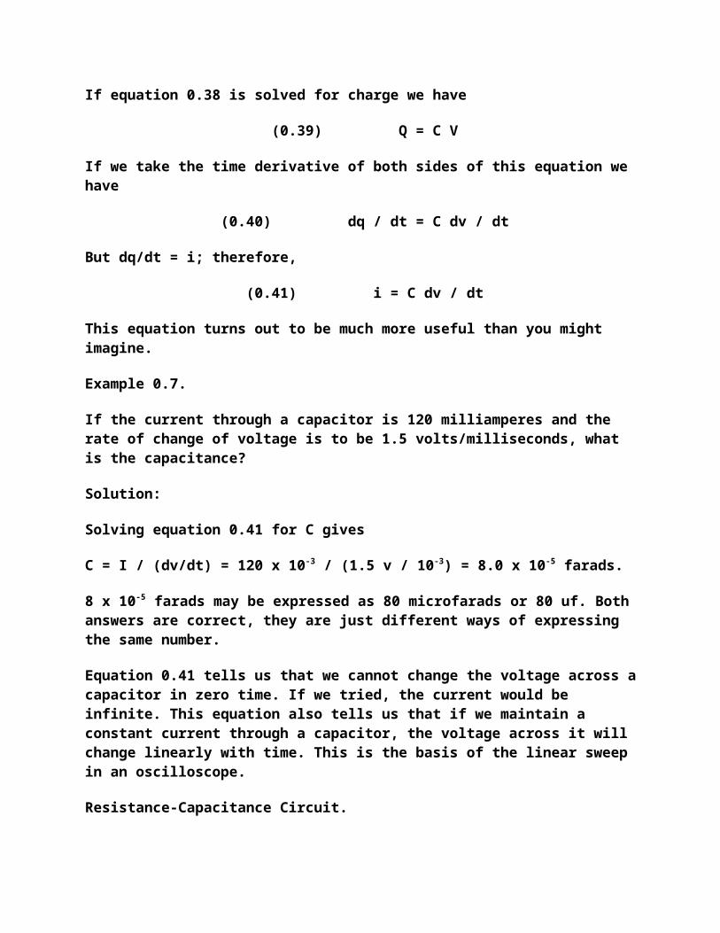
Figure 0.10 Circuit For Charging and Discharging a Capacitor.
For a verbal description click here.
Consider the circuit of Figure 0.10. The switch is placed in position 1 to insure that there is no initial charge on the capacitor. Then the switch is changed to position 2 and the capacitor begins to charge. The bottom plate will receive a negative charge while the top
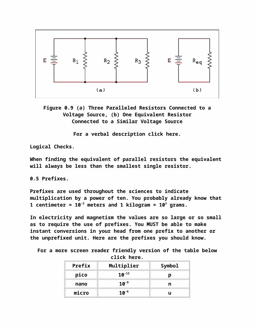
plate will receive a positive charge. Kirchhoff's voltage equation for this circuit at any instant of time is
(0.42) E = iR + q / C The battery voltage E, the resistance R and the capacitance C do not vary with time. The current i and the charge on the capacitor q do vary with time. If we take the time derivative of this equation we have
(0.43) E = di / dt x R + dq / dt x 1 / C If we make the substitution i = dq/dt we have
(0.44) E = di / dt x R + i / C The solution to this differential equation in i is
i = E / R x e-t/RC (0.45) This equation tells us that the current starts out as if the capacitor were a short circuit. i0+ = E/R. The current quickly falls away and decays exponentially.
When t becomes equal to RC the value of the exponent on e is -1. This point in time has been defined as the time constant of the circuit and is given as
(0.46) T = RC where T is the time-constant in seconds, R is the resistance in ohms and C is the capacitance in farads.
After one time-constant the current has fallen to 1/e of its initial value; after 2 time-constants the current has fallen to e-2 of its initial value and so on. Theoretically the current will never reach zero. After 5 time-constants the current will be .07% of its initial value and for most practical purposes may be considered to be zero.
Example 0.8.
Starting with equation 0.45 and using only Ohm's and Kirchhoff's laws show that the voltage across the capacitor is given by
vC = E (1 - e-t/RC (0.47) )
Solution:
The voltage across the resistor is vR = iR or
vR = E e-t/RC (0.48)
Solving Kirchhoff's equation for vC gives
(0.49) vC = E - vR
Substituting equation 0.48 into 0.49 and factoring out an E gives us
vC = E (1 - e-t/RC (0.50) )
0.8 Inductance.
Inductance is that electrical property which resists changes in the current in the circuit containing the inductance.
A device which has the property of inductance is called an inductor. It consists of a coil of wire. The coil may be wound on a solid iron core, a powdered iron core or a hollow tube (air core).
An inductor can store and release energy. The energy is stored in the magnetic field which is produced by the current flowing in the coil of wire.
Inductance is defined as
(0.51) L = N H / I where L is the inductance which is given in units called henrys, N is the number of turns on the coil, H is the magnetic flux produced by each turn and I is the current in the coil.
If we rearrange equation 0.51 we have
(0.52) L I = N H If we take the time derivative of equation 0.52 we have
(0.53) L di / dt = N dH / dt Remember from physics that
(0.54) E = - N dH /dt Substituting equation 0.54 into equation 0.53 yields
(0.55) E = - L di / dt This equation tells us that we cannot change the current through an inductor in zero time. To do so would require an infinite voltage across the inductor.
The minus sign in equation 0.55 tells us that the polarity of the voltage which is produced is in such a direction as to oppose the change which produced it.
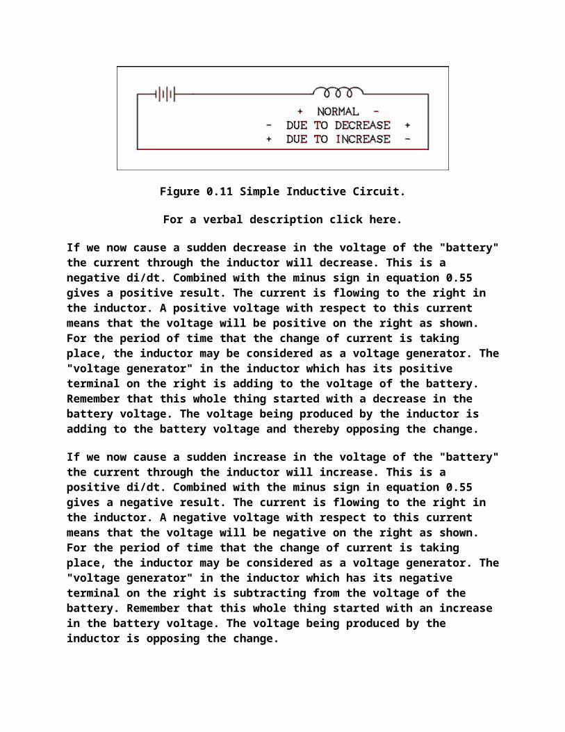
Consider the circuit of Figure 0.11. The battery will cause current to flow to the right in the inductor (coil of wire). The normal polarity of the voltage drop across the inductor will be positive to the left as shown in the figure.
Figure 0.11 Simple Inductive Circuit.
For a verbal description click here.
If we now cause a sudden decrease in the voltage of the "battery" the current through the inductor will decrease. This is a negative di/dt. Combined with the minus sign in equation 0.55 gives a positive result. The current is flowing to the right in the inductor. A positive voltage with respect to this current means that the voltage will be positive on the right as shown. For the period of time that the change of current is taking place, the inductor may be considered as a voltage generator. The "voltage generator" in the inductor which has its positive terminal on the right is adding to the voltage of the battery. Remember that this whole thing started with a decrease in the battery voltage. The voltage being produced by the inductor is adding to the battery voltage and thereby opposing the change.
If we now cause a sudden increase in the voltage of the "battery" the current through the inductor will increase. This is a positive di/dt. Combined with the minus sign in equation 0.55 gives a negative result. The current is flowing to the right in the inductor. A negative voltage with respect to this current means that the voltage will be negative on the right as shown. For the period of time that the change of current is taking place, the inductor may be considered as a voltage generator. The "voltage generator" in the inductor which has its negative terminal on the right is subtracting from the voltage of the battery. Remember that this whole thing started with an increase in the battery voltage. The voltage being produced by the inductor is opposing the change.
The inductor only has a finite amount of energy stored in its magnetic field and it cannot maintain the voltage indefinitely. The inductor cannot prevent the change in current but it can slow it down.
Example 0.9.
A relay coil has an inductance of 95 millihenrys. A transistor switch turns off a current of 40 mA through the coil in a time of 1 us. What is the magnitude of the voltage spike which is produced?
Solution:
E = L di / dt = 95 mH x 40 mA / 1 us = 3800 volts.
Resistive-Inductive Circuits.
Figure 0.12 is the diagram of an inductive-resistive (RL) circuit. The switch is placed in position 1 to insure that there is no current in the circuit. When the switch is changed to position 2 the battery's potential is applied to the series RL circuit. For an infinitesimal instant of time, no current will flow in the circuit. The inductor has developed an emf of the polarity indicated in the figure. If the voltage across the battery and the inductor have the same magnitude and sign, Kirchhoff's law says that there is no voltage drop across the
resistor. If there is no voltage across the resistor, there is no current through it. Because this is a series circuit, no current in the resistor means no current anywhere in the circuit. This situation cannot last for any finite length of time. Current begins to increase in the circuit but the change continues to be opposed by the inductor. The inductor ultimately loses the fight and the current becomes equal to E/R assuming that the inductor has zero resistance (a highly invalid assumption as it turns out).
Figure 0.12 Resistive-Inductive Circuit With Switch.
For a verbal description click here.
Now let us write Kirchhoff's equation for the circuit of Figure 0.12. (0.56) E = iR + L di / dt
The solution to this equation is i = E / R (1 - e-tR/L (0.57) )
This equation tells us that the current starts out as if the inductor were an open circuit. i0+ = 0. The current quickly rises to exponentially approach E/R.
The voltage across the inductor is
vL = E e-tR/L (0.58) Verification of equation 0.58 is left as an exercise for the student.
When t becomes equal to L/R the value of the exponent on e is -1. This point in time has been defined as the time constant of the circuit and is given as
(0.59) T = L/R where T is the time-constant in seconds, R is the resistance in ohms and L is the inductance in henrys.
After one time-constant the current has risen to 1 - 1/e of its initial value; after 2 time-constants the current has risen to 1 - e-2 of its initial value and so on. Theoretically the
current will never reach the maximum value of E/R. After 5 time-constants the current will be 99.83% of E/r and for most practical purposes may be considered to be E/r.
The Reality of Inductors.
In the foregoing, inductance and resistance were treated as if they were separate components of the circuit. In practice, inductors always have resistance. Inductors are coils of wire. Wire has resistance. It is impossible to make an inductor which does not have any resistance.
For purposes of circuit analysis the inductance of a coil and its resistance are shown schematically as separate circuit elements. In the circuit of Figure 0.12 it is likely that the resistor and inductor which are shown actually represent a single coil of wire. Think of it as being roughly analogous to the X and Y components of a force.
Recent advances in superconductors may eventually make the preceding paragraphs unnecessary. However, at the present time, it is not possible to form superconducting materials into a wire and wind it into a coil. Note: That's still true in 2007.
0.9 Problems.
1. Two spheres are charged with +25 and +50 microcoulombs respectively. The distance between them is 20 meters. What is the force exerted between the two spheres? Is the force attractive or repulsive?
2. Express the ampere in terms of kilograms, meters and seconds. 3. If a current of 500 mA flows for 11 minutes, how much charge is moved? 4. If a charge of 1026 coulombs was transferred at a constant rate in a time of 3 hours,
what was the current? 5. A current of 25 mA must be left on until a charge of 10,000 coulombs has been
moved. How long must the current be left on? Express your answer in days, hours, minutes and seconds.
6. Express the volt in terms of kilograms, meters and seconds. 7. If 300 joules of work are done on 25 coulombs of charge, what was the potential
through which the charge was moved? 8. If 12 coulombs are moved through a potential of 120 volts, how much work was
done? 9. If 420 joules of work are done while moving a certain amount of charge through a
potential difference of 28 volts, how much charge was moved? 10. If 15 amperes are drawn from a 12 volt battery, what is the power? 11. What is the current drawn by a 100 watt, 120 volt light bulb? 12. For proper operation an electroplating cell requires the movement of 1.26 x 10⁵
coulombs per hour. The cell voltage is 3.3 volts. How much power is required to keep the cell in continuous operation?
13. Express the ohm in terms of kilograms, meters and seconds. 14. A current of 55 mA is flowing through a 270 ohm resistor. What is the voltage drop
across the resistor?
15. When a potential of 12 volts is applied to an unknown resistor, a current of 24.74 mA flows. What is the resistance of the resistor?
16. If a 56 ohm resistor is placed across a 15 volt power supply, how much current will flow?
17. A resistor substitution box contains the following resistor values.
First decade 15, 22, 33, 47, 68 and 100 ohms Second decade 150, 220, 330, 470, 680 and 1000 ohms
Each successive decade follows the same pattern. The highest resistance is 10 Megohms. Each resistor can dissipate a maximum of 1 watt without burning out. (a) What is the minimum resistance setting which can be safely connected across the 120 volt power line?(b) What is the minimum resistance setting which can be safely connected across a 20 volt power supply?(c) What is the minimum resistance setting which can be safely connected across a 12 volt power supply?(d) What is the minimum resistance setting which can be safely connected across a 5 volt power supply?
18. How much current can safely be run through; (a) a 39 ohm 1/2 watt resistor, (b) a 470 ohm 1/4 W resistor, (c) a 27 ohm 2 W resistor and (d) a 560 ohm 1 W resistor?
19. In Figure 0.2, E = 6.60 volts, R1 = 33 ohms, R2 = 22 ohms and R3 = 11 ohms. How much current is flowing in the circuit?
20. In Figure 0.2, E = 7.20 volts, R1 = 470 ohms, R2 = 220 ohms and R3 = 100 ohms. What is (a) the voltage across R1, (b) the voltage across R2 and (c) the voltage across R3?
21. In Figure 0.2, R1 = 2.2 k ohms, R2 = 1.5 k ohms and R3 = 3.6 k ohms. If the voltage across R1 (V1) is 2.45 volts, what is the voltage across R3 (V3)?
22. In Figure 0.2, E = 22.5 volts, R1 = 3.9 k ohms, R3 = 4.7 k ohms, V2 = 7.500 v and V3 = 8.198 v. What is the resistance of R2?
23. In Figure 0.6, E = 6.60 volts, R1 = 33 ohms, R2 = 22 ohms and R3 = 11 ohms. How much current is flowing in the circuit?
24. In Figure 0.6, the battery current I = 200 mA, R1 = 470 ohms, R2 = 220 ohms and R3 = 100 ohms. What is; (a) the current through R1, (b) the current through R2 and (c) the current through R3?
25. In Figure 0.6, R1 = 2.2 k ohms, R2 = 1.5 k ohms and R3 = 3.6 k ohms. If I1 = 8.182 mA, what is I3?
26. In Figure 0.6, I = 5.987 mA, R1 = 3.9 k ohms, R3 = 4.7 k ohms, I2 = 1.765 mA, and I3 = 1.915 mA. What is the resistance of R2?
27. How much charge is stored on a 7000 uf capacitor when it is charged to a voltage of 18 volts?
28. A circuit has a capacitance of 100 pf. How much current must the circuit deliver to the capacitor in order to change the voltage at a rate of 13 v/us?
29. If a 2000 uf capacitor is being discharged with a current of 1 A, how much will its voltage change in 8 ms?
30. In the circuit of Figure 0.10 if R = 1 Meg ohm, C = 1 uf and E = 10.0 v. The capacitor starts out fully discharged. How long after the switch is thrown to position 2 does the voltage across the capacitor reach 9.0 volts?
31. A time delay circuit triggers when the voltage reaches 2/3 of the applied voltage. The capacitor always starts charging from 0 volts. It is desired that the circuit will trigger 1.5 seconds after the timing cycle begins. If the capacitor is a 0.1 uf, what value resistor is required in the circuit?
32. Starting with equation 0.57 and using only Ohm's and Kirchhoff's laws show that the voltage across an inductor is given by vL = E e-tR/L.
33. The current through a 50 millihenry inductor is to be changed from some value IL to zero in a time of 5 us. What must the value of IL be to give a 20 kv voltage spike?
34. What is the time-constant of a coil which has 8 henrys of inductance and 40 ohms of resistance?
35. A relay is a device which employs an electromagnet to close one or more sets of switch contacts. The switch contacts can carry a much larger current than is required to energize the electromagnet. The electromagnet is a coil of wire which has inductance and resistance. A given relay is taking too long to close its contacts in a particular application. It has been determined that the delay is not due to mechanical inertia of the moving parts but is due to the time- constant of the RL circuit of the coil. Discuss what may be done to shorten the time required for the relay to close. The relay itself may not be replaced or altered.
0.10 Answers to problems.
1. 3.125 Newtons repulsive. 2. Coulombs = meters x Newtons-1 / seconds. 3. 330 coulombs. 4. 95 mA. 5. 4 d: 15 h: 6 m: 40 s. 6. Volts = Newton-1 x seconds 7. 12 volts. 8. 1440 Joules. 9. 15 Coulombs. 10. 180 watts. 11. 0.833 Amps. 12. 115.5 watts. 13. ohms = seconds2 / meters 14. 14.85 volts. 15. 485 ohms. 16. 268 mA. 17. (a) 15 k ohms, (b) 470 ohms, (c) 150 ohms, (d) 15 ohms. 18. (a) 113 mA, (b) 23.1 mA, (c) 272 mA, (d) 42.2 mA. 19. 100 mA. 20. (a) 4.28 volts, (b) 2.00 volts, (c) 0.911 volts. 21. 4.01 volts. 22. 4.30 k ohms.
23. 1.10 Amps. 24. (a) 25.5 mA, (b) 54.5 mA, (c) 120 mA. 25. 5.00 mA. 26. 5.10 k ohms. 27. 0.126 Coulombs. 28. 1.30 mA. 29. 4.00 volts. 30. 2.30 seconds. 31. 13.6 Meg ohms. 32. Beginning with the equation,
i = E / R (1 - e-tR/L)
The voltage across the resistor is obtained by multiplying the current by the resistance. Multiplying the equation by R gives,
VR = E (1 - e-tR/L)
By Kirchhoff's law,
E = VR + VL
Or
VL = E - VR
Subtracting E from the equation for VR
VL = E - E (1 - e-tR/L)
Removing the parentheses and carrying out the multiplication gives,
VL = E - E + E e-tR/L
So,
VL = E e-tR/L
QED.
33. 2.00 Amps. 34. 0.200 seconds. 35. Place a resistor in series with the coil and increase the applied voltage to keep the
current the same.
Electrical Fundamentals. Chapter 0 Electrical Quantities From Mechanical 0.1 Quantities. Resistance and Ohm's Law. 0.2 Series Circuits and Kirchhoff's Voltage Law. 0.3 Parallel Circuits and Kirchhoff's Current Law. 0.4 Prefixes. 0.5 Numerical 0.6 Examples. Capacitance. 0.7 Inductance. 0.8 0.9 Problems.0.10 Answers to Problems.
DC Circuits. Chapter 1
Solving Complex Circuits Using Loop 1.1 Equations. Voltage Dividers. 1.2 Thevenin's Theorem. 1.3 1.4 Norton's Theorem. Current Measurement, the 1.5 D'Arsonval Meter. Voltage Measurement. 1.6 Measurement Using Multimeters. 1.7 Problems. 1.8 Answers to 1.9 Problems.
Chapter 1.
DC Circuits.It may be said that after mastering the contents of chapter 0 we have in hand all of the tools we need to solve any electric network we are likely to encounter. While this is true, there are a great many shortcuts and additional theorems to be learned. It is not possible to cover all of these. We will cover a few of the most useful ones here.
1.1 Solving Complex Circuits Using Loop Equations.
There is a theorem in network analysis which states that the total current flowing in any circuit element is the sum of the individual currents produced by each voltage source with all other sources removed and replaced by short circuits. This is called the superposition
theorem. This theorem tells us that it is possible to solve for the individual components of current and add them together to obtain the total current.
We could remove the two sources, one at a time, from the circuit of Figure 1.1 and use circuit reduction to find the values of current being drawn, or injected into, each battery, but this is still an arduous method.
Instead we will consider that current flows round and round each loop and where two currents pass through the same resistor The actual current is the algebraic sum of the two. We assume a direction for the currents because we can't always figure out the current direction by inspection. We will sum the voltages around each loop of a circuit according to Kirchhoff's voltage law.
Voltage Rises and Drops.
The least confusing way to sum voltages around a loop is to give a rise a positive sign and a drop a negative sign. That's simple isn't it? Going up is positive, going down is negative. To sum voltages around a circuit you select a starting point, it doesn't matter where, and move around the circuit until you come back to the same point. If you travel across something from minus to plus you have traversed a rise. If you traverse from plus to minus it is a drop.
A battery is not automatically a rise. What matters is which way you walked across it. If you walk from plus to minus it is a drop. Similarly a resistor is not automatically a drop. If you move across it from minus to plus it is a rise. It depends on which way you go not whether it is a battery or a resistor.
Obviously assigning the plus and minus signs is key to solving a circuit. If the signs are wrong the answer will be wrong. First of all a battery is what it is. If current is flowing out of the battery, normal discharging, or into the battery, charging, the positive side is positive and the negative side is negative. That cannot change.
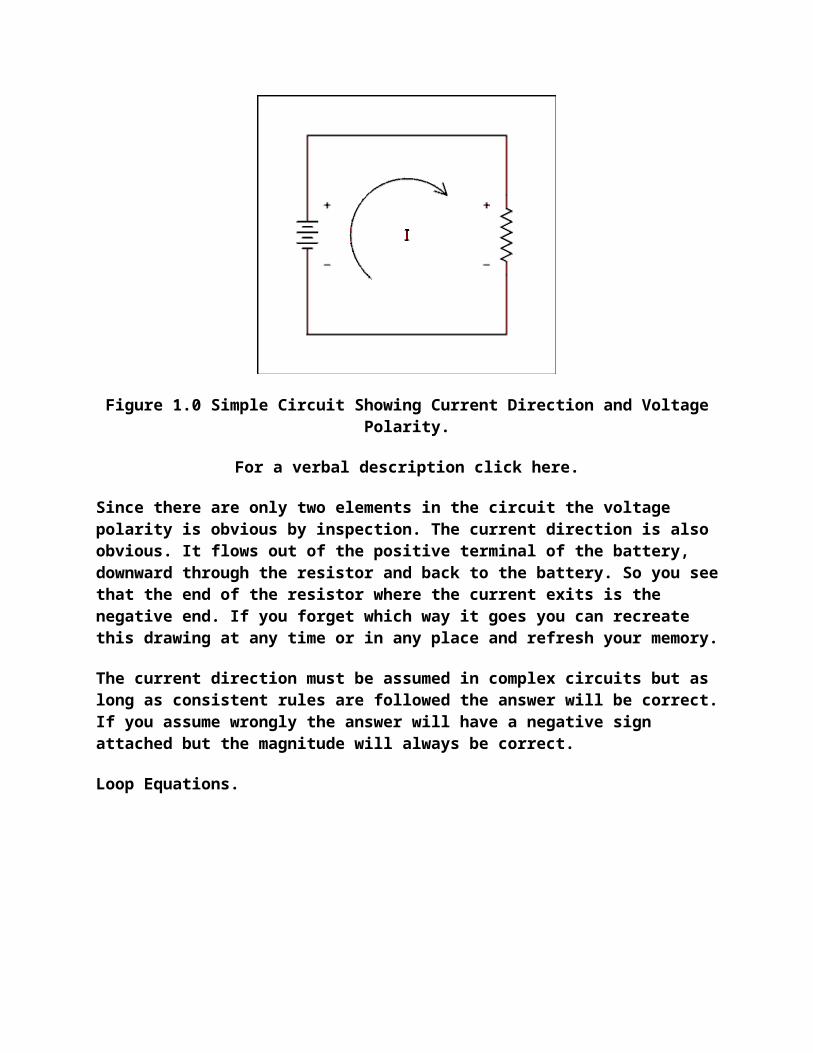
A resistor is a somewhat different story. The direction of current through the resistor determines the polarity of voltage across it. The current flows into the positive end and out of the negative end. This can be made clear with the simplest of all possible circuits.
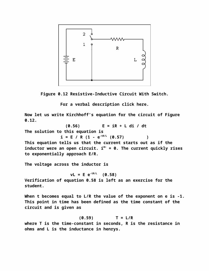
Figure 1.0 Simple Circuit Showing Current Direction and Voltage Polarity.
For a verbal description click here.
Since there are only two elements in the circuit the voltage polarity is obvious by inspection. The current direction is also obvious. It flows out of the positive terminal of the battery, downward through the resistor and back to the battery. So you see that the end of the resistor where the current exits is the negative end. If you forget which way it goes you can recreate this drawing at any time or in any place and refresh your memory.
The current direction must be assumed in complex circuits but as long as consistent rules are followed the answer will be correct. If you assume wrongly the answer will have a negative sign attached but the magnitude will always be correct.
Loop Equations.
Figure 1.1 Circuit Containing Two Voltage Sources.
For a verbal description click here.
Consider the circuit of Figure 1.1. Instead of trying to solve for the voltage and current at each resistor we will take a somewhat different approach. Assume that the current in each loop follows a closed path as indicated by the arrows in Figure 1.1. The current I1 flows through E1, R1 and R2. The current I2 flows through R2, R3 and E2. The current in R1 is I1 while the current in R3 is I2. The current in R2 is the algebraic sum of I1 and I2.
We cannot tell by inspection which direction the current in each loop is flowing. You might say "obviously the current is flowing out of the positive terminal of each battery." You might be right, you might be wrong. Suppose that E1 is the power source in a battery charger and E2 is the battery which is being charged. In that case the directions indicated by the arrows would be correct. If E2 were the source and E1 were the battery being charged the true current directions would be opposite to those shown in the figure. The true current directions may or may not be as you would tend to assume by inspection. The point is, you cannot tell in advance what the directions of the currents will be. The usual procedure is to assume that all currents are clockwise. If the guess is wrong, the answer will come out with a minus sign attached and we will know that the true current is in the opposite direction.
There are two unknowns in the circuit, I1 and I2. The circuit will produce two equations. A circuit with three loops would produce three equations in three unknowns. In general then it can be said that a network with N loops will produce N equations in N unknowns.
It is assumed that the student at this level of study has already mastered at least one technique for solving systems of N by N equations. Solving systems of 3 by 3 or larger is a job best left to a computer program. We are here to learn techniques, not to get exercise from solving systems of N by N equations. For this reason the problems and examples in this text will not exceed systems of 2 by 2.
Writing the Equations.
To write the equations we sum the voltage rises around each loop. It does not matter that there are branches in and out of the loop. Kirchhoff's voltage law applies. In the circuit of Figure 1.1 the equations are written as follows.
E1 - R1 I1 - R2 I1 + R2 I2 (1.1) = 0
- E2 - R3 I2 - R2 I2 + R2 I1 (1.2) = 0
The polarity of the voltage sources is fixed and cannot change. The polarity of each resistor drop is marked inside of each loop. Moving in the direction of assumed current, E1 is a rise and therefore positive. The drops across R1 and R2 due to I1 are drops and therefore negative. The current in loop 2 has an influence on loop 1 and so we must include this in the equation. The term "R2 I2" reflects this influence. The term is positive because the voltage difference produced by I2 is a rise when moving in the direction of I1. In loop 2 (equation 1.2) the voltages due to I2 are all drops and therefore negative as is E2. The only positive term in equation 1.2 is the effect of I1 on loop 2.
It may seem as if there is some magic going on here. Each equation is just a statement of Kirchhoff's voltage law for that loop. The techniques for writing these equations were covered in chapter 0. If you do not understand how to write these equations, review section 0.3.
Assuming that the individual currents run in circles may be a little more difficult to understand. Intuition and visualization tell us that the currents really don't do that. However, this is a mathematical model. Mathematical models do not necessarily describe physical reality; they permit calculations to be made which will give the right answer.
Do not attempt to memorize equations 1.1 and 1.2. Learn how to write the equations from the circuit as it is given.
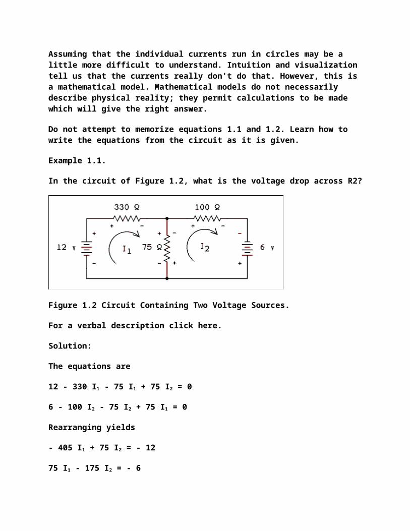
Example 1.1.
In the circuit of Figure 1.2, what is the voltage drop across R2?
Figure 1.2 Circuit Containing Two Voltage Sources.
For a verbal description click here.
Solution:
The equations are
12 - 330 I1 - 75 I1 + 75 I2 = 0
6 - 100 I2 - 75 I2 + 75 I1 = 0
Rearranging yields
- 405 I1 + 75 I2 = - 12
75 I1 - 175 I2 = - 6
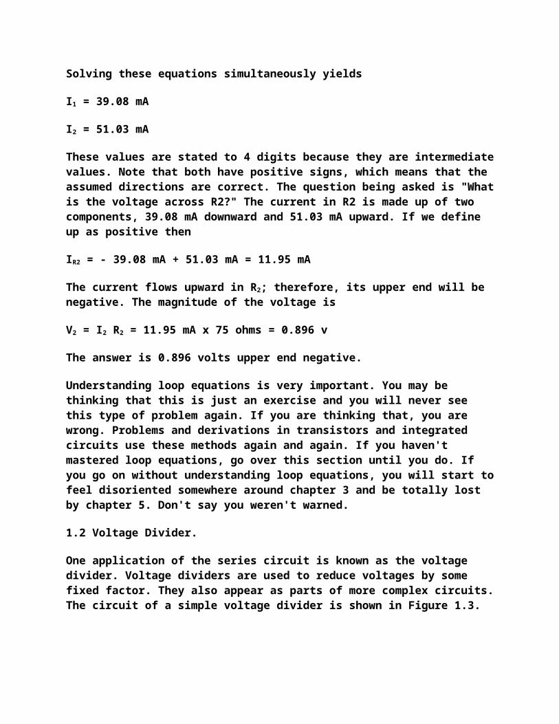
Solving these equations simultaneously yields
I1 = 39.08 mA
I2 = 51.03 mA
These values are stated to 4 digits because they are intermediate values. Note that both have positive signs, which means that the assumed directions are correct. The question being asked is "What is the voltage across R2?" The current in R2 is made up of two components, 39.08 mA downward and 51.03 mA upward. If we define up as positive then
IR2 = - 39.08 mA + 51.03 mA = 11.95 mA
The current flows upward in R2; therefore, its upper end will be negative. The magnitude of the voltage is
V2 = I2 R2 = 11.95 mA x 75 ohms = 0.896 v
The answer is 0.896 volts upper end negative.
Understanding loop equations is very important. You may be thinking that this is just an exercise and you will never see this type of problem again. If you are thinking that, you are wrong. Problems and derivations in transistors and integrated circuits use these methods again and again. If you haven't mastered loop equations, go over this section until you do. If you go on without understanding loop equations, you will start to feel disoriented somewhere around chapter 3 and be totally lost by chapter 5. Don't say you weren't warned.
1.2 Voltage Divider.
One application of the series circuit is known as the voltage divider. Voltage dividers are used to reduce voltages by some fixed factor. They also appear as parts of more complex circuits. The circuit of a simple voltage divider is shown in Figure 1.3.
Figure 1.3 Simple Voltage Divider.
For a verbal description click here.
The following is based on a voltage divider with no significant load. The output voltage is the voltage across R2. To find the voltage across R2 we need to find the current through it. The current through R2 is the same as the current anywhere else in the circuit. The current in the circuit is given by
I = E / (R1 + R2 (1.3) ) The voltage across R2 is given by
VO = I R2 (1.4) Substituting equation 1.3 into equation 1.4 gives us the voltage divider equation
VO = E R2 / (R1 + R2 ) (1.5) This is one of the most often used equations in electricity and electronics. Although memorization is usually not recommended, make an exception for this one. Remember not only the equation but the procedure for obtaining it.
Often the input voltage to a voltage divider is not a battery E but sometimes a known voltage VIN. In this case the equation would be
VO = VIN R2 / (R1 + R2 (1.6) ) If the voltage divider has more than two resistors the equation is basically the same. The numerator is the sum of all of the resistors the output is taken across. The denominator is the sum of all resistors in the divider chain. An example will illustrate.
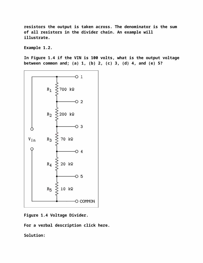
Example 1.2.
In Figure 1.4 if the VIN is 100 volts, what is the output voltage between common and; (a) 1, (b) 2, (c) 3, (d) 4, and (e) 5?
Figure 1.4 Voltage Divider.
For a verbal description click here.
Solution:
(a) When the output is taken from common and point 1, the output is connected to the input by wires. The output voltage is 100 volts.
V (b) O = VIN (R2 + R3 + R4 + R5) / (R1 + R2 + R3 + R4 + R5)
VO = 100 v x 300 k ohms / 1000 k ohms = 30 v
V (c) O = 100 v x 100 k ohms / 1000 k ohms = 10 v
V (d) O = 100 v x 30 k ohms / 1000 k ohms = 3 v
V (e) O = 100 v x 10 k ohms / 1000 k ohms = 1 v
1.3 Thevenin's Theorem.
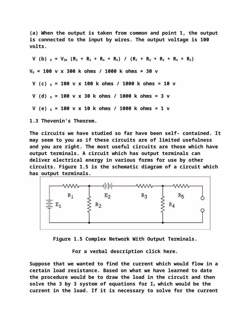
The circuits we have studied so far have been self- contained. It may seem to you as if these circuits are of limited usefulness and you are right. The most useful circuits are those which have output terminals. A circuit which has output terminals can deliver electrical energy in various forms for use by other circuits. Figure 1.5 is the schematic diagram of a circuit which has output terminals.
Figure 1.5 Complex Network With Output Terminals.
For a verbal description click here.
Suppose that we wanted to find the current which would flow in a certain load resistance. Based on what we have learned to date the procedure would be to draw the load in the circuit and then solve the 3 by 3 system of equations for I3 which would be the current in the load. If it is necessary to solve for the current in a number of different loads, the system of equations must be solved as many times as there are loads. Enter Thevenin.
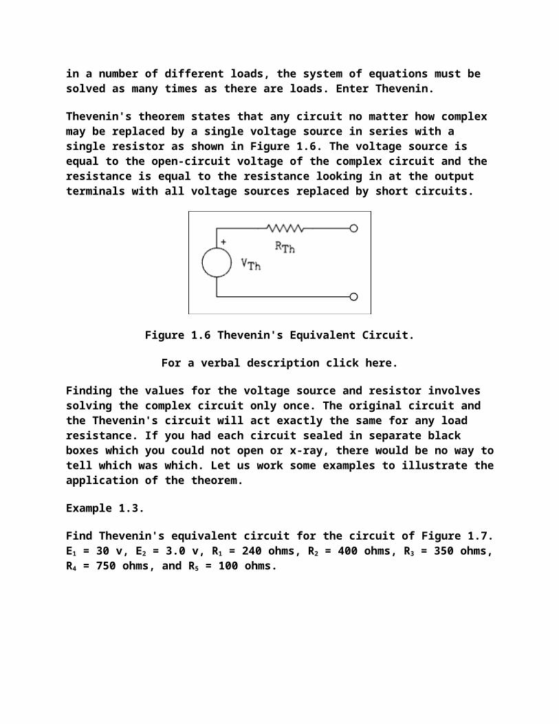
Thevenin's theorem states that any circuit no matter how complex may be replaced by a single voltage source in series with a single resistor as shown in Figure 1.6. The voltage source is equal to the open-circuit voltage of the complex circuit and the resistance is equal to the resistance looking in at the output terminals with all voltage sources replaced by short circuits.
Figure 1.6 Thevenin's Equivalent Circuit.
For a verbal description click here.
Finding the values for the voltage source and resistor involves solving the complex circuit only once. The original circuit and the Thevenin's circuit will act exactly the same for any load resistance. If you had each circuit sealed in separate black boxes which you could not open or x-ray, there would be no way to tell which was which. Let us work some examples to illustrate the application of the theorem.
Example 1.3.
Find Thevenin's equivalent circuit for the circuit of Figure 1.7. E1 = 30 v, E2 = 3.0 v, R1 = 240 ohms, R2 = 400 ohms, R3 = 350 ohms, R4 = 750 ohms, and R5 = 100 ohms.
Figure 1.7 Circuit For Example 1.3.
For a verbal description click here.
Solution:
In the circuit of Figure 1.7 if the output is open-circuited there will be no current in R5. I3 = 0. If there is no current in R5 there is no voltage drop across it. The output voltage is the same as the voltage across R4. This effectively reduces the problem from a 3 by 3 to a 2 by 2. The only unknowns are I1 and I2 and there are two loops to give us two equations.
E1 - R1 I1 - R2 I1 + R2 I2 = 0
E2 - R2 I2 - R3 I2 - R4 I2 + R2 I1 = 0
Substituting Values.
30 - 240 I1 - 400 I1 + 400 I2 = 0.
3 - 400 I2 - 350 I2 - 750 I2 + 400 I1 = 0.
Combining and rearranging.
-640 I1 + 400 I2 = - 30.
400 I1 - 1500 I2 = - 3.
We need to know I2 but don't care what I1 is. Multiplying the second equation by 1.6 gives.
-640 I1 + 400 I2 = - 30.
640 I1 - 2400 I2 = - 4.8.
Adding the two gives.
0 I1 - 2000 I2 = - 34.8.
I2 = - 34.8 / (- 2000) = 17.40 mA.
I2 is the only current flowing through R4 so.
VR4 = VTh = 17.40 mA x 750 ohms = 13.05 volts.
Now we must obtain the Thevenin resistance.
Figure 1.8 Figure 1.7 With Voltage Sources Removed and replaced by short circuits.
For a verbal description click here.
The Thevenin resistance is the resistance at the terminals with all voltage sources removed and replaced by short circuits. The method here is to start farthest from the terminals and start combining resistors. R1 and R2 are in parallel so.
R12 = R1 R2 / (R1 + R2) = 240 x 400 / (240 + 400) = 150 ohms.
R12 and R3 are in series so.
R123 = R12 + R3 = 150 + 350 = 500 ohms.
R123 is in parallel with R4 so.
R1234 = R123 R4 / (R123 + R4) = 300 ohms.
R1234 and R5 are in series so.
R12345 = RTh = R1234 + R5 = 400 ohms.
Figure 1.9 Thevenin's Equivalent Circuit of Figure 1.7
For a verbal description click here.
Example 1.4.
Use Thevenin's theorem to solve example 1.1. "In the circuit of Figure 1.2, what is the voltage drop across R2?"
Solution:
Because the voltage across R2 is what is wanted, we will treat R2 as a load resistor and remove it from the circuit. The result is shown in Figure 1.10.
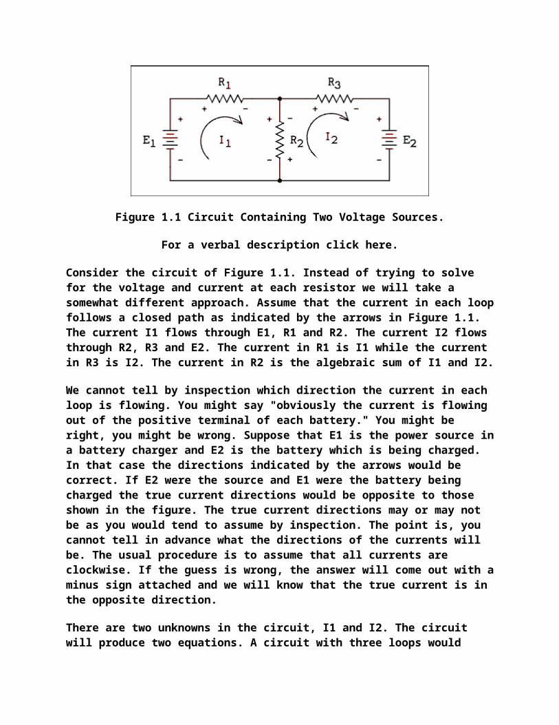
Figure 1.10 Figure 1.2 With R2 Removed.
For a verbal description click here.
We will now write the loop equation around the outside loop to determine the current in the two resistors which are now simply in series.
12 - 330 I - 100 I + 6 = 0
18 = 430 I
I = 18 v / 430 ohms = 41.86 mA.
Now we will write the loop equation around the loop of the 12 volt battery, the 330 ohm resistor, and the load terminals. Don't be concerned that the load terminals are open. It is easily possible to have a voltage existing across an open circuit. The load voltage is what we want to know.
12 - 330 I - VL = 0
VL = 12 - 330 I = 12 - 13.814 = - 1.814 volts.
This is the Thevenin's voltage source for the equivalent circuit. If both voltage sources are replaced by short circuits the two resistors are in parallel with each other. The equivalent resistance is 76.74 ohms . This is the Thevenin's resistance for the circuit. Now we draw the Thevenin's circuit and connect R2 to it, Figure 1.11
Figure 1.11 Thevenin's Equivalent CircuitWith R2 Connected as a Load.
For a verbal description click here.
Now we apply the voltage divider equation to determine the voltage across R2.
VR2 = -1.814 v x 75 ohms / (75 ohms + 76.74 ohms) = -0.897 v
Maybe we should have carried 5 digits in our intermediate results. The error in the third decimal place is a result of using a finite number of significant digits, not any defect in either method of solution.
Thevenin's theorem can also be used on circuits so complex that they cannot easily be analyzed mathematically. An example is the function generator used in the laboratory. An electronics engineer could study the schematic diagram of the generator and calculate the Thevenin's resistance (also known as output resistance) of the generator. If the function generator had not yet been constructed a calculation would be the only way to find the Thevenin's resistance (or output resistance) of the generator.
Example 1.5.
When the function generator has no load connected, its output voltage is 7.87 volts. When a 100 ohm resistor is connected as a load the voltage is 5.20 volts. What is the output resistance of the function generator?
Solution:
The Thevenin's voltage source is always equal to the open-circuit output voltage of any Thevenin's circuit. Figure 1.12 shows the circuit with everything we know about it to date.
Figure 1.12 Thevenin's Equivalent Circuitof a Function Generator
For a verbal description click here.
You could apply the voltage divider equation and solve it for the unknown resistor. But suppose that this is a test and you don't remember how to do that. The proper procedure is to put the best computer ever designed to work on the problem, the human mind. Kirchhoff's voltage law gives the voltage drop across the unknown resistor.
V? = VTh - VL = 7.87 - 5.20 = 2.67 v
Ohm's law gives the current through RL.
IL = VL / RL = 5.20 V / 100 ohms = 52.0 mA.
Kirchhoff's current law gives the current through the unknown.
I? = IL = 52.0 mA.
Ohm's law gives the resistance of the unknown.
R? = V? / I? = 2.67 v / 52.0 mA = 51.3 ohms.
The output resistance is 51.3 ohms.
Thevenin's theorem can be used: 1) to solve for the load conditions in circuits which have output terminals, 2) to simplify circuits by allowing a key resistor to be removed and 3) to find the output resistance of devices such as signal generators even when we do not know what is in the box. This is why it can be said that Thevenin's theorem is one of the most useful theorems in circuit analysis.
1.4 Norton's Theorem.
The Ideal Current Source.
Before we look at ideal current sources let us look at what we know about ideal voltage sources. An ideal voltage source will maintain a constant voltage across its terminals regardless of the amount of current being drawn. The ideal voltage source will keep its voltage constant even if it has to deliver an infinite amount of current to do so. Do I hear someone saying "That's impossible!"? This is an ideal voltage source. In the ideal case, anything is possible.
An ideal voltage source delivers zero power when it is open-circuited. In the open-circuit case, the current is zero. If the current is zero, the power is zero.
We are accustomed to thinking of open-circuits as being a "zero power" condition and short-circuits as being damaging. In the real world any attempt to take anything to infinity is usually damaging to something.
Items we normally think of as voltage sources, such as batteries, are actually Thevenin's equivalent circuits with very low values of output resistance.
An ideal current source will maintain a constant current through its terminals regardless of the amount of voltage being delivered. The ideal current source will keep its current constant even if it has to deliver an infinite amount of voltage to do so. Do I hear someone saying "That's impossible!"? This is an ideal current source. In the ideal case, anything is possible.
An ideal current source delivers zero power when it is short-circuited. In the short-circuit case, the voltage is zero. If the voltage is zero, the power is zero.
We are NOT accustomed to thinking of short-circuits as being a "zero power" condition and open-circuits as being damaging. In the real world any attempt to take anything to infinity is usually damaging to something. An open-circuit current source will attempt to go to infinite voltage and that is an undesirable condition.
The Theorem.
Norton's theorem states that any circuit no matter how complex may be replaced by a single current source in parallel with a single resistor as shown in figure 1.13. The current source is equal to the short-circuit current of the complex circuit and the resistance is equal to the resistance looking in at the output terminals with all voltage sources replaced by short circuits and any current sources replaced by open circuits.
Figure 1.13 Norton's Equivalent Circuit.
For a verbal description click here.
Norton's theorem is not used as often as Thevenin's theorem but it can make short work of example 1.2. Pun fully intended.
Example 1.6.
Use Norton's theorem to solve example 1.2. "In the circuit of Figure 1.2, what is the voltage drop across R2?"
Solution:
Figure 1.14 shows the circuit with R2 removed and replaced by a short circuit. This completely isolates the two loops so they cannot affect one another.
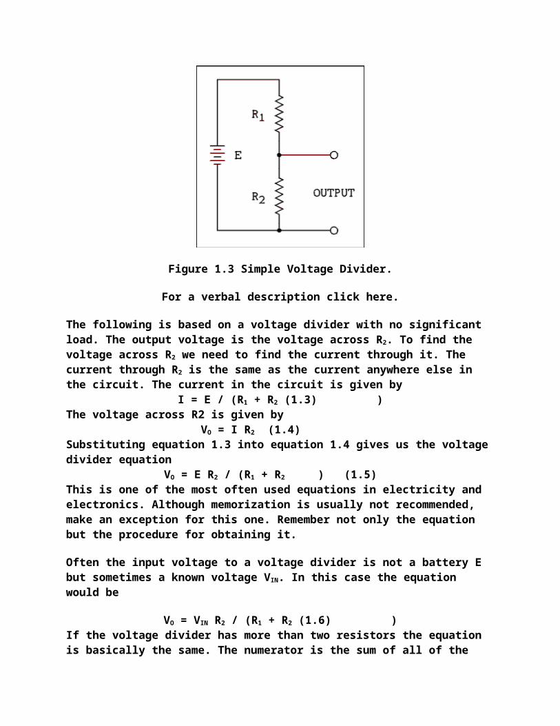
Figure 1.14 Figure 1.2 with R2 Replaced by a Short.
For a verbal description click here.
The current due to the loop on the left is
I1 = 12 v / 330 ohms = 36.364 mA downward.
The current due to the loop on the right is.
I2 = 6 v / 100 ohms = 60.000 mA upward.
With up defined as positive, the current in the short is.
IS = 60.000 mA - 36.364 mA = 23.636 mA upward.
To make current flow upward in the load, current must flow out of the bottom terminal of the current source. The Norton's resistance is the same as the Thevenin's resistance, which is 76.744 ohms . Thus we have the circuit as shown in Figure 1.15 which shows R2 restored to the circuit.
Figure 1.15 Norton's Equivalent of Figure 1.2.
For a verbal description click here.
The current source delivers its 23.636 mA to the parallel combination of RN and R2. The voltage across R2 is the current source multiplied by the parallel combination of RN and R2.
VR2 = -23.636 mA / (1/75 + 1/76.744) = -0.897 v
Thevenin Meets Norton.
Example 1.7.
Find Thevenin's and Norton's equivalent circuits for the circuit of Figure 1.16.
Figure 1.16 Voltage Divider Circuit.
For a verbal description click here.
Solution:
The Thevenin voltage is the open-circuit output voltage of the circuit. This voltage is given by the voltage divider equation as follows.
VTh = 30 v x 1 k ohm / (1 k ohm + 2 k ohms) = 10 v
When the battery E is replaced by a short circuit, R1 and R2 are in parallel and their equivalent resistance is RTh = 666.7 ohms. The circuit would be that of Figure 1.9 except the values will be the ones calculated here. For Norton's theorem the current is equal to the short- circuit current of the original circuit. With a short on the output terminals, R2 is completely shorted out and the current is determined by R1 and the battery.
IN = 30 v / 2 k ohms = 15 mA
The Norton resistance RN is equal to the Thevenin resistance RTh.
If you place a short on a Thevenin's equivalent circuit the current will be given by
I = VTh / RTh (1.7) If you open-circuit a Norton's equivalent circuit the output voltage is given by
V = IN RN (1.8) The two circuits must behave exactly alike or one or both of the theorems would be invalid. In equation 1.7, the current I is the short-circuit current which is the same as the Norton's current source and, therefore, is IN. In equation 1.8, the voltage V is the open-circuit voltage which is the same as the Thevenin's voltage source. In reality then, the two equations are one which can be written as
RTh = RN = VTh / IN (1.9) If you have any two of these three quantities, you can find the other one. Depending on the circuit it may be easier to find the short-circuit current and the open-circuit voltage. You may want to do this even though you have not been asked to find Norton's equivalent circuit.
1.5 Current Measurement, the D'Arsonval Meter.
The measurement of current is basic to many electrical measurements. For example the measurement of voltage is accomplished by setting up a circuit of known resistance, placing the unknown voltage across the circuit and measuring the current in the circuit. Other quantities (resistance for example) are converted to current for reading on a meter.
The D'Arsonval Meter Movement.
Figure 1.17 Diagram of a D'Arsonval Meter Movement.
For a verbal description click here.
A D'Arsonval meter movement consists of 4 basic parts. A permanent magnet, a coil of fine wire which is suspended so it can pivot, a pointer attached to the coil, and a scale for the pointer to point to. Figure 1.17 shows only the magnet and coil with its pivot and support. The circular object with a cutout at one point is the permanent magnet. The field is concentrated in the small circular cutout at the bottom. The red object is the coil of fine wire. The support is shown in green. The coil is supported by taught metal bands which provide spring tension to return the pointer to zero when no current is flowing through the coil. The pointer and scale have been omitted to avoid making the drawing too complicated to draw.
When a current is applied to the coil of wire, the magnetic field created by the current interacts with the field of the permanent magnet which causes a torque to be applied to the coil. The torque is opposed by the springs according to the equation
T = K Theta where T is the torque, K is the spring constant and Theta is the angle of deflection. An equilibrium will be established at some given angle which is also the deflection of the pointer. If the current in the coil is doubled, the torque will be doubled and the angle of deflection will have to be doubled to establish a new equilibrium. The angle of deflection of the moving part of the meter is directly proportional to the current in the coil. A linear scale may be marked off and used to read current without any conversion graph.
Measuring Current.
The schematic symbol for a meter is a circle with one or more letters inside to indicate the quantity which the meter can measure. Occasionally the letter G for galvanometer or M for meter is used. A D'Arsonval meter measures the current which flows through its own coil. Thus, if we want to measure a current, we must allow that current to flow through the meter. Let us look at the circuit of a flashlight which was used in chapter 0 and is shown in Figure 1.18a. If we want to measure the current in this circuit we open the circuit and insert the meter as shown in Figure 1.18b. Because this is a simple series circuit, it makes no difference where the meter is inserted.
Figure 1.18 (a) Flashlight, (b) With Current Meter Inserted
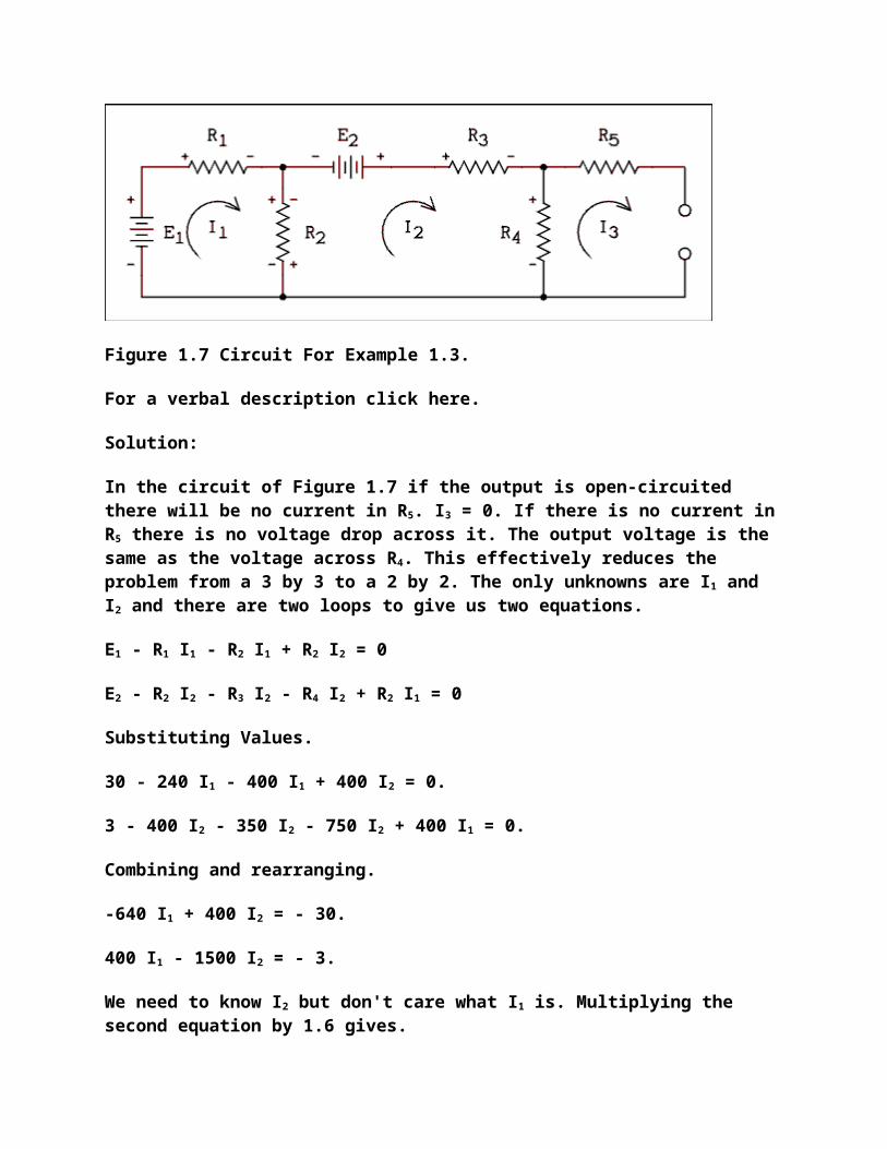
For a verbal description click here.
If we desired to set up the circuit of Figure 1.2 to measure the currents we would have to be careful where the meters were inserted. If we want accurate measurements of I1 and I2 the meters must be inserted in places where only these currents are flowing. That is to say the branch containing R2 must not have one of the meters in it. A meter connected here would measure the algebraic sum of I1 and I2. Figure 1.19 shows how to connect the meters to measure I1 and I2. Since we do not know the directions of the currents the polarity of the meters will have to be determined experimentally. In other words if the pointer goes backward, reverse the connections to the meter.
Figure 1.19 Figure 1.2 With Current Meters Inserted.
For a verbal description click here.
Because current meters are connected in series with the circuits they are measuring, any voltage drop across the meter is lost to the circuit. The voltage drop across the meter must be kept small or inserting the meter will seriously disturb the circuit under test. By Ohm's law, to keep the voltage drop small, the resistance must be small. The typical resistance of a meter will cause a voltage drop of 100 mV (millivolts) when the meter is indicating full scale. That means that a typical meter which reads 1 ampere full-scale will have a resistance of R = 0.1 v / 1 A = 0.1 ohms.
An all-too-common student mistake is to connect an ammeter in parallel with a low resistance Thevenin source. If the above meter were to be connected across a 12 volt battery, how much current would flow through the meter?
I = 12 v / 0.1 ohms = 120 Amps. A current of 120 amperes will virtually and instantly destroy a meter designed to read 1 ampere full-scale. When in the laboratory (or anywhere else for that matter), don't connect an ammeter or milliammeter across a power supply or battery.
Extending the Range of the Meter Movement.
Meter movements are most often sold in two common forms. One requires 50 uA (microamps) for full-scale deflection and the other requires 1 mA for full-scale deflection.
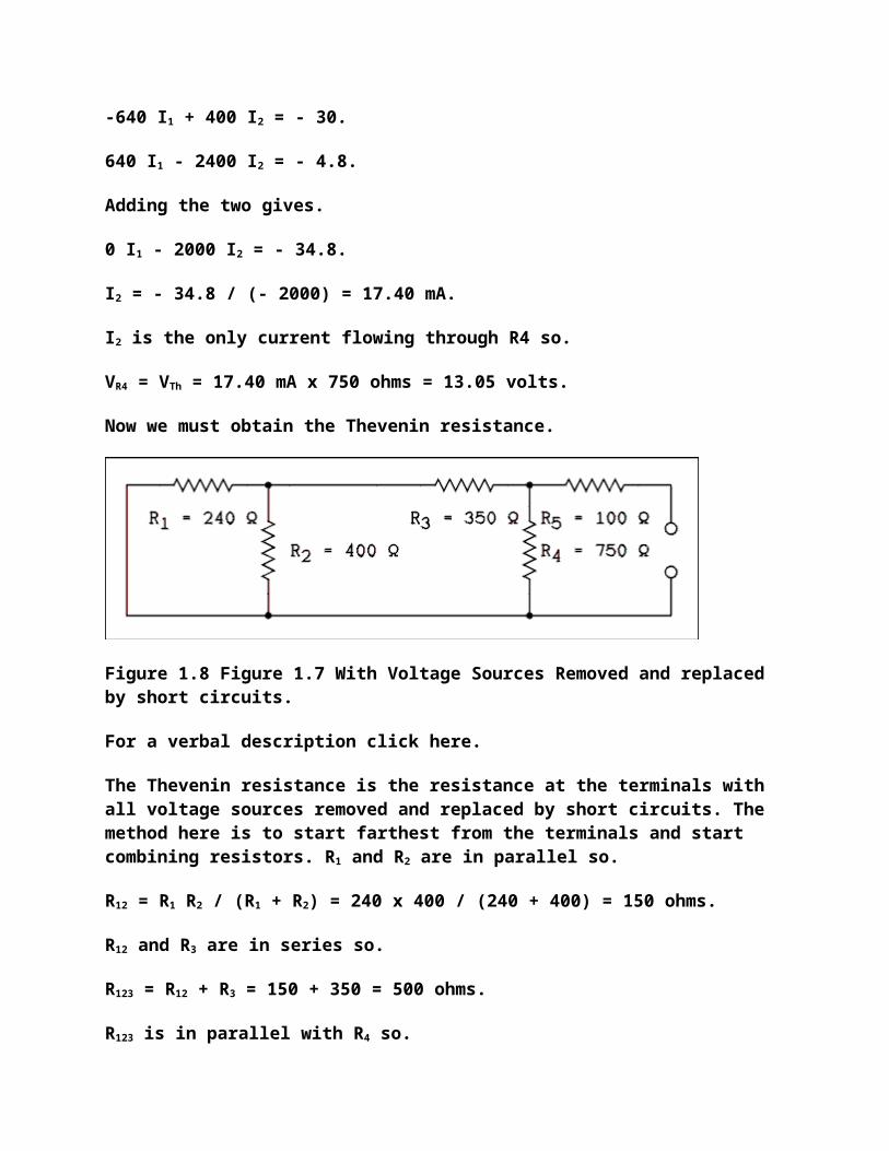
These are sometimes referred to as 0-50 uA and 0-1 mA but most often are called 50 uA and 1 mA meters. Meters which come from the manufacturer with different full-scale currents are most likely one of the aforementioned types with one or two resistors added to extend the range to a higher current.
The process of adding a resistor to extend or increase the range of a meter is known as shunting the meter. The resistor which is added is called a shunt resistor. A meter with a shunt resistor connected is shown in Figure 1.20. The logical reasoning for determining the value of the shunt resistor is as follows.
Figure 1.20 Meter With Shunt Resistor Connected.
For a verbal description click here.
1. The desired full-scale current I, the meter's full-scale current IM and the meter's resistance RM will be given.
2. The voltage across the meter may be calculated by VM = IM RM (by Ohm's law). 3. The voltage across the shunt resistor is the same as the meter voltage (by
Kirchhoff's voltage law). 4. The current in the shunt resistor is IS = I - IM (by Kirchhoff's current law). 5. The value of the shunt resistor is RS = VM / IS (by Ohm's law).
For those who prefer them, the equation for this is RS = IM / (I - IM (1.10) )
Example 1.8.
A meter movement has a full-scale current of 50 uA and a resistance of 1800 ohms . Calculate the value of the shunt resistor to extend the range of the meter to 200 uA.
Solution:
The voltage drop across the meter is
VM = 50 uA x 1800 ohms = 90 mv
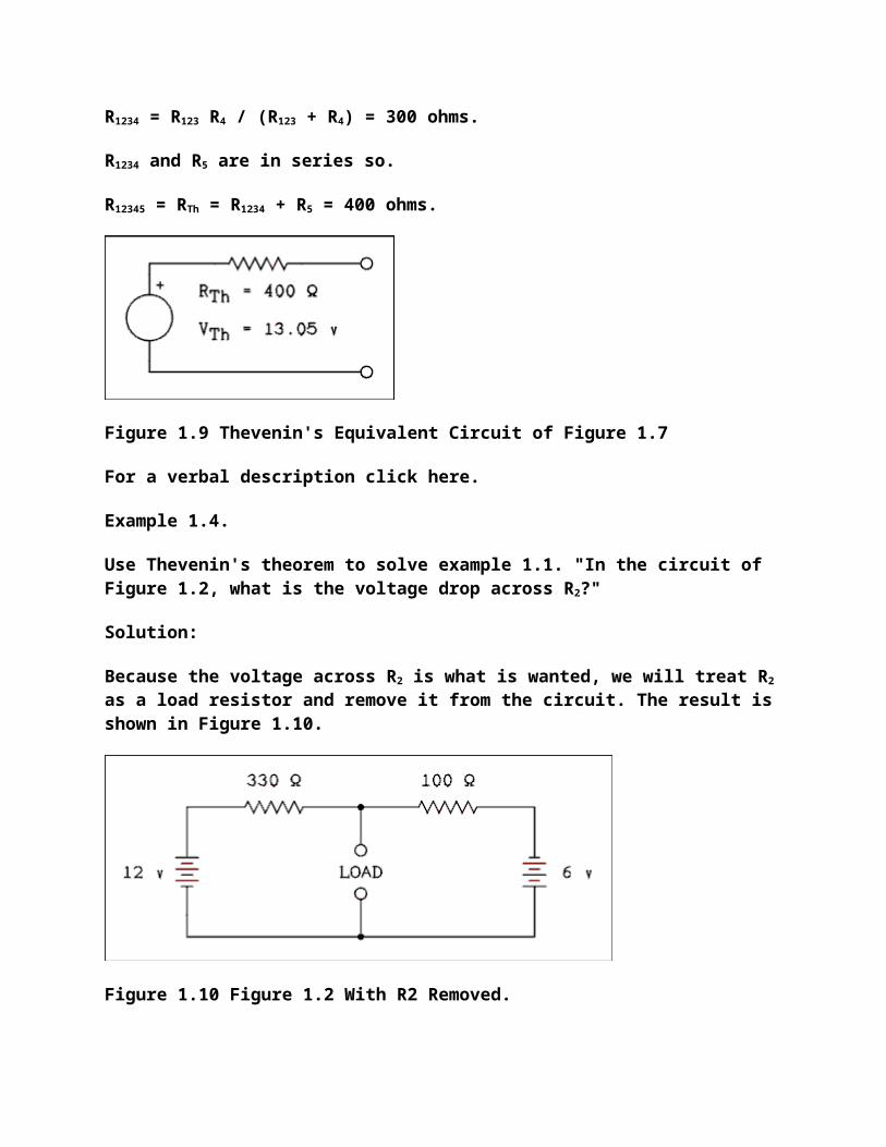
The voltage across the shunt resistor is also 90 mv. The current through the shunt resistor is
IS = 200 uA - 50 uA = 150 uA
The resistance of the shunt resistor is
RS = 90 mv / 150 uA = 600 ohms.
The Two Resistor Current Shunt.
The resistors which are used in meter circuits must be precise if the meter is to give precise readings. Precision resistors are often difficult for a person working in a physics lab to find. If a second resistor is added to the circuit as shown in Figure 1.21 the value of the shunt resistor may take on a higher value than the one indicated for the single resistor circuit.
Figure 1.21 Meter With Two Resistor Shunting Circuit.
For a verbal description click here.
The steps for using this circuit are as follows. 1. Use the procedure (or equation 1.10) given above to determine the minimum value
for the shunt resistor. 2. Locate a resistor close to, but above, the calculated value. 3. Calculate the voltage drop across this new shunt resistor by the equation VS = IS
RS. The value of IS has not changed. 4. Calculate the total resistance of the meter branch by RMT = VS / IM. 5. Calculate the resistance of R1 by R1 = RMT - RM.
The equation is as follows. R1 = RS (I - IM) - IM RM / IM (1.11)
Example 1.9.
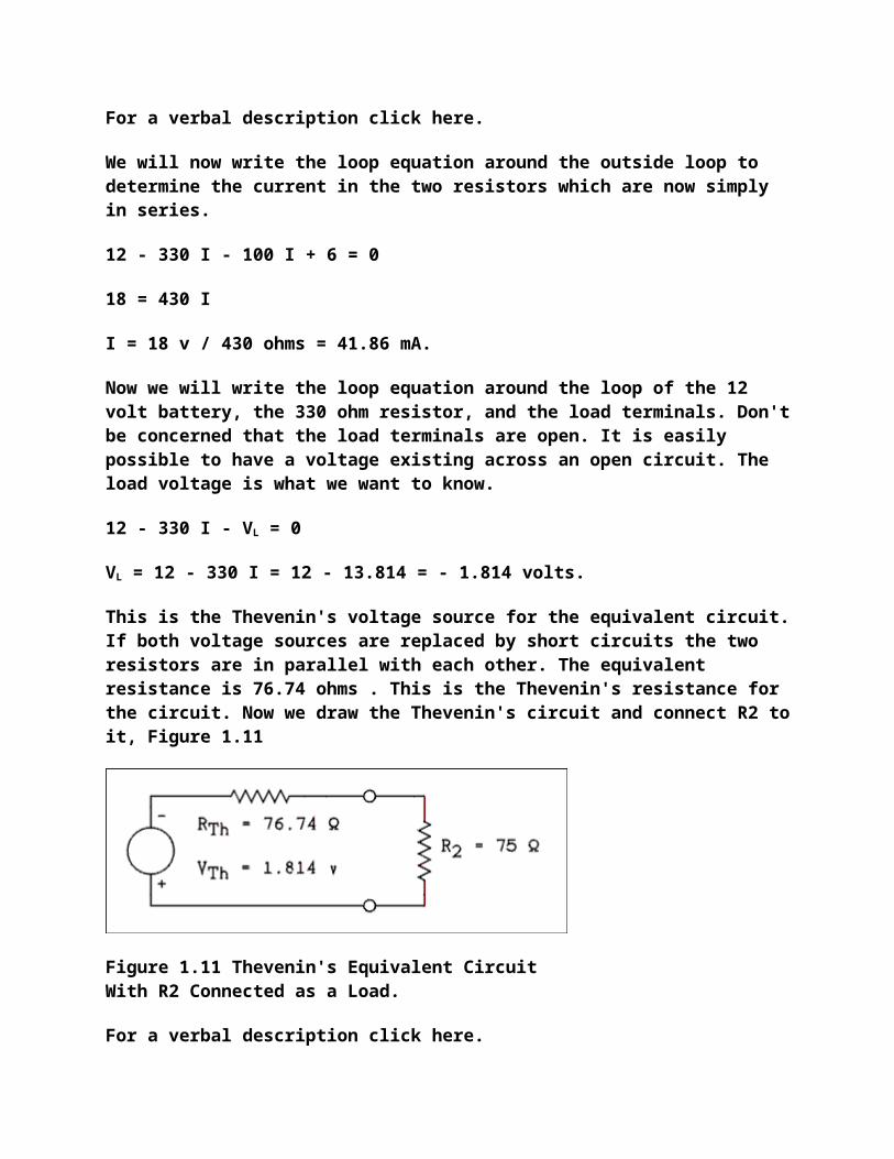
After working out the answer to example 1.8, you go to the stockroom and locate a 750 ohm precision resistor. Calculate the value of R1 in Figure 1.21 to permit the 750 ohm resistor to be used as the shunt.
Solution:
The voltage drop across RS is
VS = 150 uA x 750 ohms = 112.50 mv
The total resistance of the meter branch is
RMT = 112.50 mv / 50 uA = 2250.0 ohms
The value of R1 is given by
R1 = 2250 ohms - 1800 ohms = 450 ohms.
What happens if you cannot find a 450 ohm resistor? To be perfectly frank, the values used in this example are in a range of resistance in which precision resistors are easy to find. A precision resistance bridge may be used to select resistors from a stock of less precise resistors. Statistically, if you look through a large stock of 470 ohms 10% resistors you will find a 450 ohm resistor. It might have been just as easy to find a 600 ohms resistor. A better example is required.
Example 1.10.
A meter with a current of 1 mA has a resistance of 88 ohms . This meter is to be shunted to allow it to have a range of 0 to 1 ampere. The following precision shunts are available in the lab: 0.01 ohms , 0.1 ohms , 0.5 ohms and 1.0 ohms . How should the meter be shunted?
Solution:
Precision shunt resistors in values less than an ohm are difficult to find. We are restricted to what is available. First, assume the circuit of Figure 1.20 and use equation 1.10 to determine the minimum value for the shunt resistor.
RS = 1 mA x 88 ohms / (1 A - 1 mA) = 0.088088 ohms.
Among the available shunt resistors the 0.1 ohm is the next highest one from 0.088088 ohms. Use the 0.1 ohm shunt in the circuit of Figure 1.21. The value of R1 as given by equation 1.11 is as follows.
R1 = 0.1 ohm (1 A - 1 mA) - 1 mA x 88 ohms / 1 mA = 11.90 ohms.
An 11.9 ohm resistor can easily be found in a bin of 12 ohm resistors.
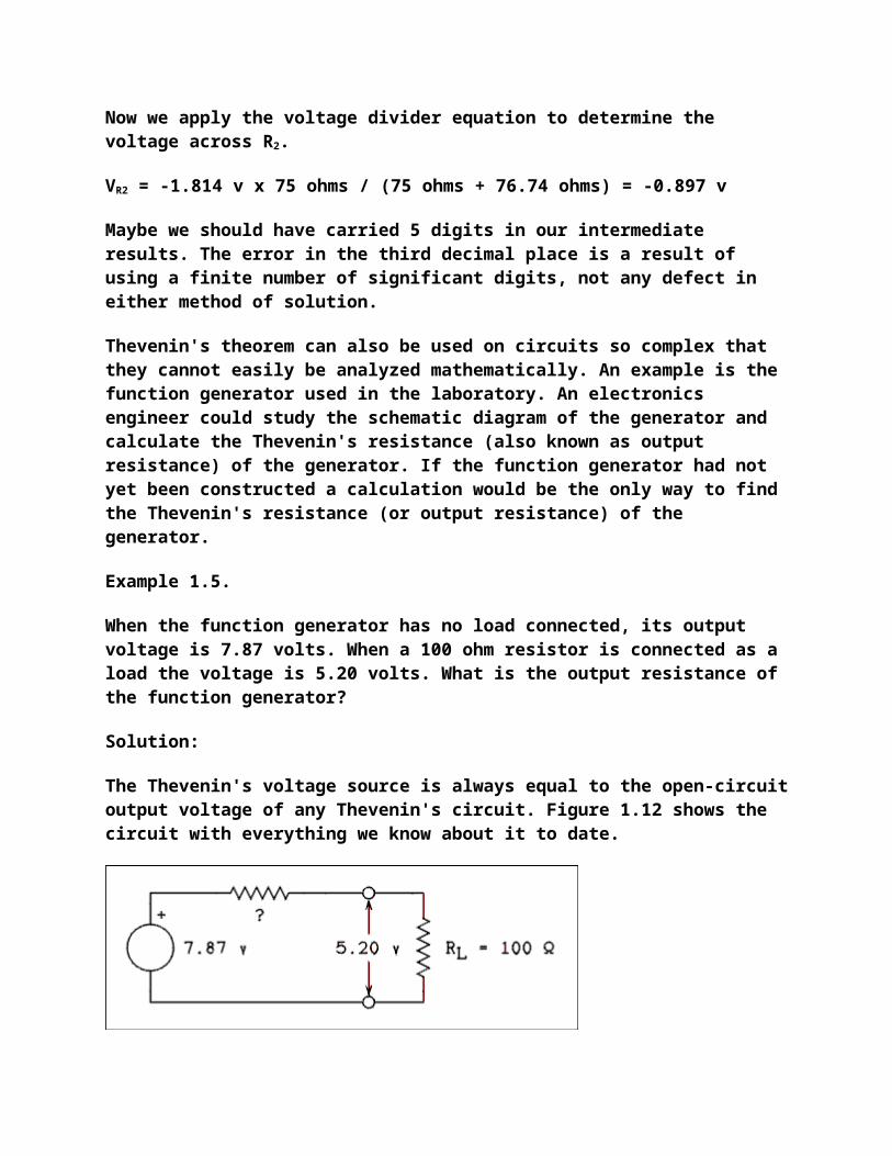
Ammeter Perturbation of a Circuit.
Figure 1.22 shows an ammeter being used to measure the current being drawn by some sort of load which is indicated as a resistor. When the ammeter is added into the circuit, its resistance adds to the resistance which is already there. If the resistance is changed, the current is changed, which means that the current we measure is not the same as the current was before the ammeter was put into the circuit. Is it possible to figure out what the current was before the ammeter was inserted? Let us list what we know and see what we can figure out.
Figure 1.22 Ammeter Connected to Measurethe Current Drawn by a Load
For a verbal description click here.
1. We know the resistance of the ammeter, (RAM). 2. We know the power supply or battery voltage, (E). 3. We know the current, (I), being drawn by the series combination of the ammeter
and the load. The ammeter is telling us that.
Using these knowns, what can we figure out?
1. The voltage drop (VAM) across the ammeter. Multiply the ammeter reading (I) by the ammeter resistance (RAM).
2. The voltage dropped across the load (VL). Subtract the ammeter voltage drop (VAM) from the power supply voltage (E).
3. Load resistance (RL). Divide the voltage drop across the load (VL) by the ammeter reading (I).
4. And finally the load current before the ammeter was inserted (IL). Divide the power supply voltage (E) by the load resistance (RL).
For those who prefer an equation, it is
IL = E / (E - I x RAM (1.12) )
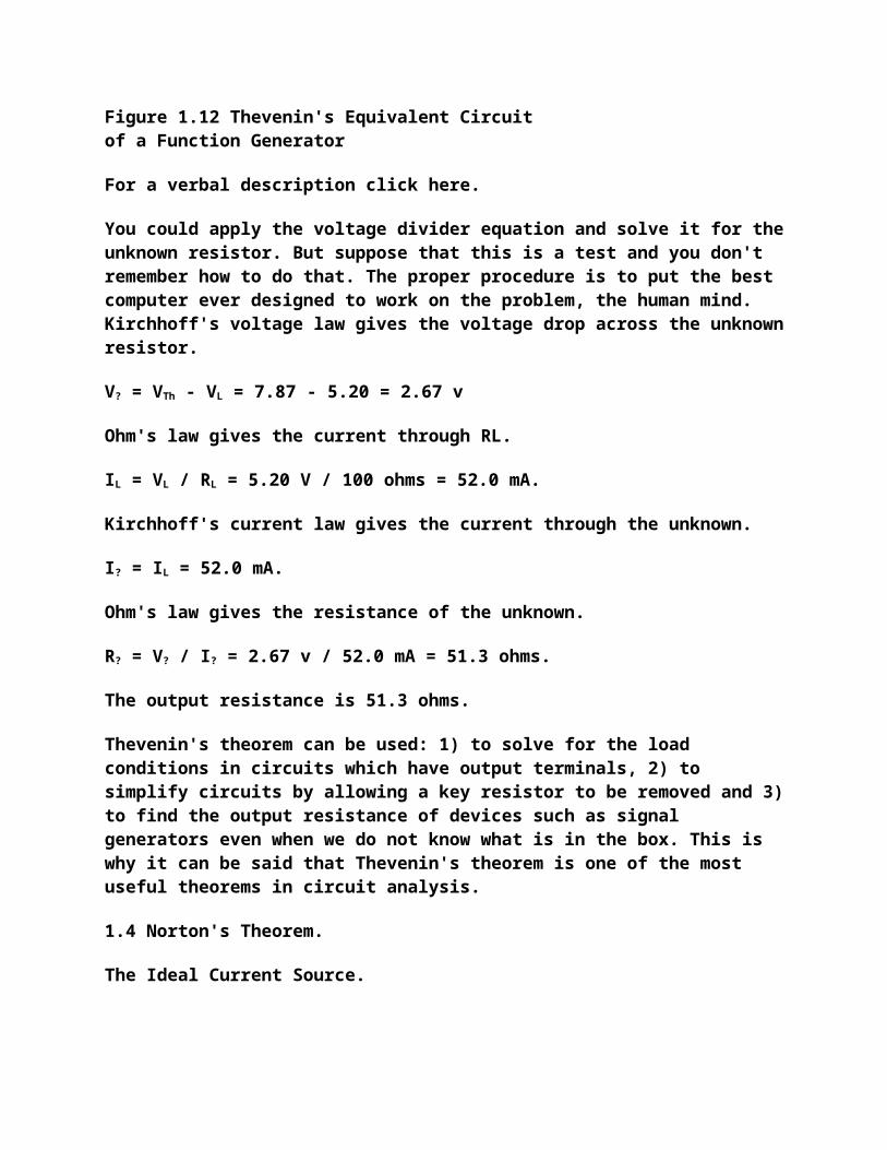
It is true that some loads are nonlinear, which means that the load resistance changes as the load voltage changes. (The load does not obey Ohm's law.) In most cases this second-order perturbation is small enough to be neglected.
Logical Check.
Remember that the insertion of an ammeter or milliammeter into a circuit will always reduce the current. The calculated load current IL must always be larger than the measured current I. If your calculated current is less than the measured current, the answer is wrong.
Example 1.11.
The 200 uA meter of example 1.8 is being used to measure the current in a load as in Figure 1.22. The power supply voltage is 5.00 volts and the meter is indicating 195 uA. What was the current in the circuit before the microammeter was inserted?
Solution:
First of all we need to calculate the resistance of the ammeter. It is the parallel combination of the 600 ohm shunt and the 1800 ohms of the meter movement. This works out to 450 ohms. The voltage drop across the microammeter is 195 uA x 450 ohms = 87.750 mv. The voltage left across the load is 5.0000 v - 87.75 mv = 4.91225 v. The resistance of the load is 4.91225 v / 195 uA = 25191 ohms. If this load were placed across 5.0000 v the current would be 5.0000 v / 25191 ohms = 198.5 uA.
Example 1.12
Calculate the percent error of the measurement in the above example.
Solution:
The calculated value of 198.5 uA is the standard of comparison or reference. The percent error is given by
(1.13) % error = 100% x (Measured - Reference) / Reference
% error = 100% x (195 uA - 189.5 uA) / 198.5 uA = -1.76%
If we substitute equation 1.12 into equation 1.13 using I as the measured value and equation 1.12 as the reference value we eventually obtain
% error = 100% x (-I) x RAM (1.14) / E
where I is the current measured by the meter, RAM is the resistance of the ammeter (milliammeter or microammeter) and E is the voltage of the power supply or battery. Another equation can be obtained by inverting ohms law.
I/E = 1/(RAM + RL) which is
% error = 100% x (-RAM) / (RAM + RL ) (1.15) if RL is known, this equation can be most useful.
Example 1.13
It is desired to measure the current to an accuracy of Plus or minus 2%. The meter has a full-scale range of 20 mA and has a voltage drop of 200 mv when reading full scale. The power supply voltage is 9.00 v and the meter reads 16.5 mA. Is this reading within plus or minus 2%?
Solution:
The meter resistance is 200 mv / 20 mA = 10 ohms. RL + RAM = 9.00 v / 16.5 mA = 545 ohms. RL = 545 ohms - 10 ohms = 535 ohms. Using equation 1.15 we have
% error = 100% x (-10 ohms) / (10 ohms + 535 ohms) = -1.83%
The measurement is of acceptable accuracy.
1.6 Voltage Measurement.
Connecting a Voltmeter Into a Circuit.
Voltage is the electrical potential difference between two points in a circuit. If it is desired to measure the potential difference between point A and point B in a circuit, the meter must be connected between points A and B. That is one lead to point A and the other lead to point B. To measure the voltage of a battery, the voltmeter is simply connected in parallel with the battery. A voltmeter is never connected in series with a circuit. Ammeters are connected in series, voltmeters are connected in parallel.
The Voltmeter Circuit.
The D'Arsonval meter is a current measuring device. As example calculations have shown its voltage drop is typically 0.1 volts. Still, it is possible to use such a meter to measure voltages over a wide range.
What is required is a circuit in which a current will flow which is proportional to the unknown voltage. The D'Arsonval meter can be used to measure the current in this circuit. Ohm's law states that I = E / R. A resistor is all that is required to cause a current to flow which is proportional to the voltage. A voltmeter circuit is shown in Figure 1.
Figure 1.23 Circuit Diagram of a Voltmeter.
For a verbal description click here.
The total resistance in the circuit is such that the full-scale current of the meter will flow when the desired full-scale voltage is applied to the circuit. The total resistance is RV + RM; therefore, an equation may be written
RV + RM = VV / IM (1.16) where VV is the full-scale voltage of the voltmeter, IM is the full-scale current of the meter movement, RM is the resistance of the meter movement and RV is the resistance of the multiplier resistor. The multiplier resistance is given by the following equation.
RV = VV / IM - RM (1.17)
Example 1.14.
Find the value of the multiplier resistor to convert a 50 uA meter into a voltmeter having a full-scale voltage of 5 volts. The resistance of the meter movement is 1800 ohms.
Solution:
The total resistance of the meter circuit is
RT = 5.00 v / 50.0 uA = 100 k ohms.
The multiplier resistor is
RV = RT - RM = 100 k ohms - 1.8 k ohms = 98.2 k ohms.
Ohms Per Volt.
Figure 1.24 is the diagram of the voltmeter of example 1.14 with an addition. It is desired to temporarily convert the 5 volt meter of example 1.14 into a 6 volt meter. As you can see in figure 1.24, this will be accomplished by adding another resistor to the circuit.
Example 1.15.
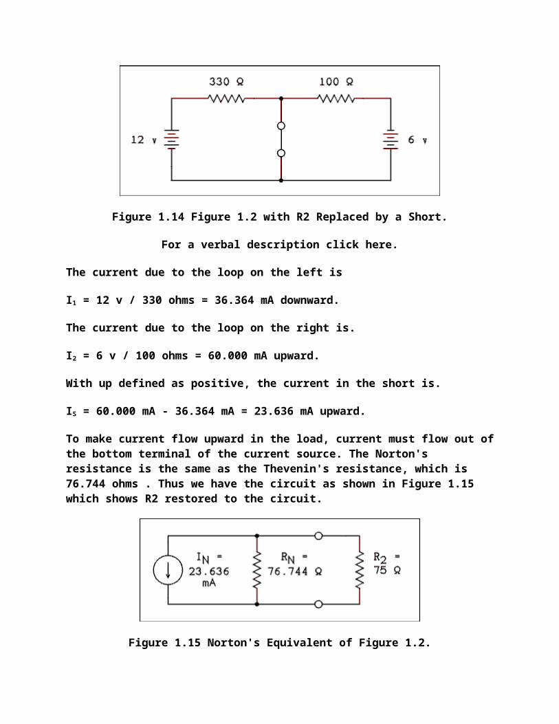
Calculate the value of RV in Figure 1.24.
Solution:
The total resistance RT = 6 v / 50 uA = 120 k ohms. But we already have 100 k ohms of resistance in the circuit. So we have RT = RV + 1.8 k ohms + 98.2 k ohms. Therefore, RV = 120 k ohms -100 k ohms = 20 k ohms.
Figure 1.24 5 volt meter with a resistor added to convert it to a 6 volt meter.
For a verbal description click here.
Example 1.16.
Calculate RV to extend the range of a 5 volt meter to 10 volts full-scale.
Solution:
The total resistance RT = 10 v / 50 uA = 200 k ohms. So we have RT = RV + 1.8 k ohms + 98.2 k ohms. Therefore, RV = 200 k ohms - 100 k ohms = 100 k ohms. Notice in examples 1.15 and 1.16 that for every volt of range extension, we must add 20,000 ohms. In example 1.15 we added 1 volt of range and to do so we added 20,000 ohms. In example 1.16 we added 5 volts of range and to do so we added 5 x 20,000 ohms or 100 kilohms.
The number 20,000 is not standard for all voltmeters but is dependent on the current of the meter movement being used. The amount of resistance to be added for each additional volt of range is given by
RAdded = 1 v / IM This is called the sensitivity of a voltmeter and is given as
S = 1 v / IM (1.18) The sensitivity of a voltmeter is a figure of merit which may be used to judge the relative quality of various voltmeters. The higher the number, the better the voltmeter.
Example 1.17.
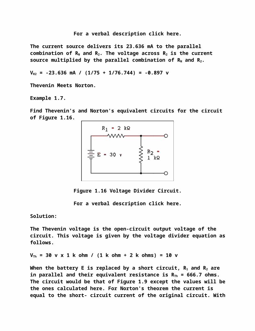
Calculate the sensitivity of a voltmeter which used a 500 uA meter movement.
Solution:
The sensitivity is
S = 1 v / 500 uA = 2,000 ohms/volt.
Voltmeter Perturbation of a Circuit.
Figure 1.25 shows a voltmeter being used to measure the output voltage of a Thevenin's circuit (voltage source and resistor). If the voltmeter resistance is too low in comparison to the Thevenin resistance, the voltmeter will perturb the circuit by a significant amount and the reading will be in error.
It is possible to determine the voltage of the Thevenin generator (voltage source) if we can determine the value of the Thevenin resistance. This can be done in many cases. Let us now list the things we know and see what we can figure out.
1. We know the resistance of the voltmeter (RVM). 2. We know the voltage drop across the voltmeter (VVM). The voltmeter itself is telling
us that. 3. We know the Thevenin resistance (RTh) of the circuit whose voltage we are trying to
measure.
Figure 1.25 Voltmeter Measuring Output of Thevenin's Equivalent Circuit.
For a verbal description click here.
The microammeter and its series resistor are included in the circle with a V in the center.
We can now calculate the following.
1. The voltmeter current (IVM). Divide the voltmeter reading (VVM) by the voltmeter resistance (RVM).
2. The current flowing through the Thevenin resistance. It is the same as the current through the voltmeter.
3. The voltage drop across the Thevenin resistance (VRTh). Multiply the current from 2 above (IVM) by the Thevenin resistance (RTh).
4. And finally, the voltage before the voltmeter was connected (VTh). Add the voltage drop across the Thevenin resistance (VRTh) to the voltmeter reading (VVM).
For those who prefer an equation, it is
VTh = VVM (RVM + RTh) / RVM (1.19)
Logical Check.
Remember that the connection of a voltmeter to a circuit will always reduce the voltage. The calculated voltage VTh must always be larger than the measured voltage VVM. If your calculated voltage is less than the measured voltage, the answer is wrong.
Example 1.18.
A meter with a full-scale voltage of 10 volts and a sensitivity of 10,000 ohms /v is being used to measure the voltage of a Thevenin's equivalent circuit as shown in Figure 1.25. The Thevenin's resistance is 10 k ohms . The meter reads 9.25 volts. What is the voltage of the Thevenin's voltage source?
Solution:
The resistance of the voltmeter is RVM = 10 v x 10 k ohms/v= 100 k ohms. The current in the voltmeter is IVM = 9.25 v / 100 k ohms = 92.5 uA. The drop across the Thevenin's resistor is VRTh = 92.5 uA x 10 k ohms = 0.925 v. The Thevenin's voltage source is 9.25 v + 0.925 v = 10.175 v.
Example 1.19.
Calculate the percent error of the measurement in the above example.
Solution:
The calculated value of 10.175 v is the standard of comparison or reference. The percent error is given by equation 1.13 as follows.
% error = 100% x (9.25 v - 10.175 v) / 10.175 v = -9.09%.
If we substitute equation 1.19 into equation 1.13 using VVM as the measured value and equation 1.19 as the reference value we eventually obtain
% error = 100% x (-RTh) / (RTh + RVM ) (1.20)
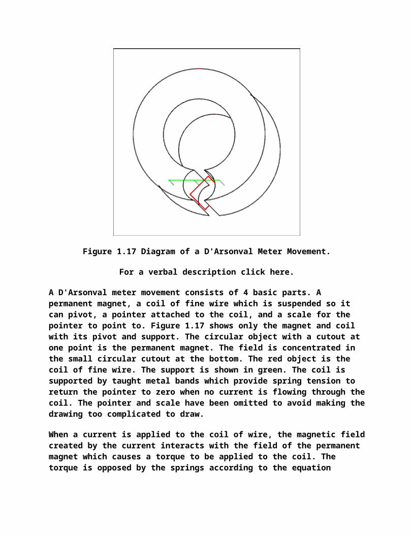
where RTh is the Thevenin's resistance of the circuit being tested and RVM is the resistance of the voltmeter.
Example 1.20.
Use equation 1.20 to verify the results of example 1.19.
Solution:
Using equation 1.20 gives
% error = 100% x (-10 k ohms) / (10 k ohms + 100 k ohms) = -9.09%.
The result is verified as correct.
1.7 Measurement Using Multimeters.
A multimeter (pronounced multi-meter) is an instrument which is capable of measuring more than one electrical quantity. The usual multimeter is capable of measuring voltage, current and resistance. Such meters are also known as volt-ohm-milliammeters or VOMs for short.
The analog multimeter (or VOM) is exemplified by the Simpson 260 which is used in the laboratory. This instrument consists of a D'Arsonval meter movement, two switches, several resistors and two diodes.
The VOM has full-scale voltage ranges from 2.5 volts to 1000 volts. The voltmeter circuit is exactly like the one studied in this chapter. To determine the input resistance of the voltmeter on any range, multiply the sensitivity by the setting of the range switch. The voltage being indicated does not affect the input resistance. The sensitivity of the Simpson VOM is 20,000 ohms per volt on DC and 5,000 ohms per volt on AC. The two diodes are used to change the AC to DC because the D'Arsonval meter will only respond to direct current.
The ammeter portion of the VOM has current ranges from 50 microamperes to 10 amperes and works only on DC. It employs a rather complex shunting arrangement which prevents the resistance of the switch contacts from affecting the accuracy of the reading. It is felt that the student would profit little from a detailed study of this shunting circuit.
The resistance or ohmmeter section of the VOM employs a battery to energize the circuit. The battery applies a known voltage to the unknown resistor and the meter measures the current which flows. The meter face incorporates a scale for reading resistance so that no calculation is necessary. Because I = V / R the scale is highly compressed at high resistance values.
The Electronic Multimeter.
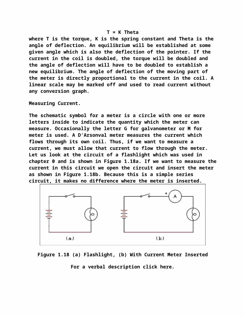
Electronic multimeters most often have a digital readout instead of a D'Arsonval meter movement. The digital readout gives better accuracy than an analog meter. If the voltage being measured has some noise on it, its value is varying slightly in a random manner, a digital meter may give confused and jumpy readings.
The thing which all electronic multimeters have in common is a complex electronic circuit which will convert a voltage into an indication on the readout device. This circuit will be studied later in this book but for now it will be treated as a mysterious black box.
The basic measurement circuit of a digital multimeter is a voltmeter which will measure from 0 to 200 millivolts. The readout is from 000.0 mv to 199.9 mv. This is called a 3 and 1/2 digit readout. The most significant digit can only be 0 or 1 and this is called a 1/2 digit. The DMMs (digital multimeters) we are using in our lab are 4-1/2 digit models which means that the basic range is from 000.00 mv to 199.99 mv. To save time and space this basic range will be referred to as a 0 to 200 mv range.
The voltmeter section of a DMM uses a voltage divider similar to that of Figure 1.4. The resistance values are R1 = 9 Meg ohms, R2 = 900 k ohms, R3 = 90 k ohms, R4 = 9 k ohms, and R5 = 1 k ohms. The input resistance of the basic measuring circuit must be very high, in excess of 10 G ohms . The unknown voltage is connected to the VIN terminals in Figure 1.4 and the measuring circuit is connected between common and one of the connection points. The voltage range selector switch is what connects the measuring circuit to the selected tap on the voltage divider. Some DMMs are auto-ranging, which means that a small microprocessor will select the proper range for the voltage which is being applied to the meter. The voltage ranges work on AC or DC. The input resistance is always 10 Meg ohms on any range on AC or DC.
For current measurements the basic measuring circuit is connected in parallel with a low-value shunt resistor. For example, if a 1 ohm resistor is used as the shunt, a current of 200 mA will cause a voltage drop of 200 mv; thus a 1 ohms shunt will provide a current range of 0 to 200 mA. To change current ranges a new shunt resistor is switched in. The current ranges work on AC or DC.
The resistance measurement circuit consists of a constant current source and the basic measuring circuit. A known current is made to flow through the unknown resistor and the resultant voltage drop is measured by the measuring circuit. For example, if a current of 100 uA flows through a 2 k ohm resistor the voltage is 200 mv; thus a current of 100 uA will give a resistance range of 0 to 2 k ohms . To change ranges the magnitude of the current is changed.
1.8 Problems.
1. In the circuit of figure 1.1 the values are as follows. E1 = 15 v, E2 = 12 v, R1 = 1 k ohm, R2 = 500 ohms, and R3 = 1.2 k ohms. What are the values of (a) I1, (b) I2, and (c) the voltage drop across R2? (d) Is the battery at E2 being charged or discharged?
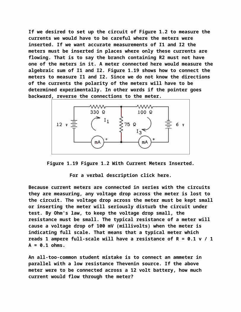
2. In the circuit of Figure 1.3 R1 = 50 ohms, and R2 = 120 ohms. If E = 6.6 v, what is the output voltage?
3. In the circuit of Figure 1.4 the values are as follows. R1 = 6.8 Meg ohms, R2 = 2.2 Meg ohms, R3 = 680 k ohms, R4 = 220 k ohms, and R5 = 91 k ohms. (a) What is the total resistance of the divider? If 100 volts are applied at VIN what is the output voltage between common and (b) point 1, (c) point 2, (d) point 3, (e) point 4, and (f) point 5?
4. In the circuit of Figure 1.3 if R2 = 3.3 k ohms, what should the resistance of R1 be for the output voltage to be one third of E?
5. In the circuit of Figure 1.3 R1 = 5.6 k ohms, and R2 = 3.3 k ohms. What must the input voltage (E) be to give an output voltage of 6.1 volts?
6. Apply Thevenin's theorem to solve problem 1. What is the voltage across R2? 7. In the circuit of Figure 1.4 use the values given in the figure. Calculate the
Thevenin's resistance if the output is between common and (a) point 1, (b) point 2, (c) point 3, (d) point 4 and (e) point 5.
8. A signal generator has an open-circuit output voltage of 8.00 volts. When a 1 k ohm resistor is connected across the output terminals, the voltage is 5.00 v. Find Thevenin's equivalent circuit for this generator. Draw the circuit!
9. Apply Norton's theorem to solve problem 1. What is the voltage across R2? 10. In the circuit of Figure 1.4 use the values given in the figure. Calculate the Norton's
resistance if the output is between common and (a) point 1, (b) point 2, (c) point 3, (d) point 4 and (e) point 5.
11. A signal generator has an open-circuit output voltage of 8.00 volts. When a 1 k ohm resistor is connected across the output terminals, the voltage is 5.00 v. Find Norton's equivalent circuit for this generator. Draw the circuit!
12. A D'Arsonval meter movement has a resistance of 1653 ohms and a full-scale current of 100 uA. Calculate the value of a single shunt resistor to make a 1 mA meter. Draw the circuit!
13. The meter movement from problem 12 is to be used in a two-resistor shunting circuit to make a 1 mA meter. The shunt resistor has the value 219.4 ohms. What is the required value of R1? Draw the circuit!
14. A milliammeter which has a full-scale current of 10 mA has a voltage drop of 250 mv when it is indicating full scale. When the meter is connected into a circuit where the voltage source is 6.00 v the meter reads 7.75 mA. (a) What was the current in the circuit before the meter was inserted? (b) What is the percent error of the measurement?
15. A D'Arsonval meter movement has a resistance of 1653 ohms and a full-scale current of 100 uA. Calculate the value of the multiplier resistor to make a 1 v meter. Draw the circuit!
16. What is the sensitivity of a voltmeter which employs a meter movement having a full-scale current of 25 uA?
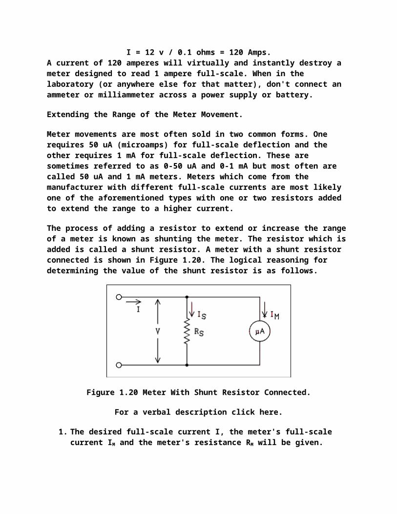
Figure 1.26 Circuit of a 5-range Voltmeter.
For a verbal description click here.
17. The circuit of Figure 1.26 is of a 5-range voltmeter. As the range switch is changed from range to range, the arrowhead moves from one circle to another. As the circuit is drawn the meter is set to the 10 volt range. The switch may be set to any range, it just happens to be shown on the 10 volt range. The meter movement has a resistance of 4476 ohms and a full-scale current of 25 uA. Calculate the resistances of (a) R1, (b) R2, (c) R3, (d) R4, and (e) R5, for the voltage ranges shown. Do not jump to conclusions, look carefully at the circuit. It may be helpful to redraw the circuit with the switch set to the voltage range you are currently working on.
18. A digital voltmeter which has an input resistance of 10 Meg ohms is being used to measure the voltage on a circuit which has a Thevenin's resistance of 470 k ohms. (a) What will be the percent error of the measurement? (b) If the indicated voltage is 8.523 volts, what was the voltage before the meter was connected to the circuit?
19. A 5,000 ohm-per-volt VOM is being used to make a measurement on a given circuit. The Thevenin's voltage and resistance of the circuit are unknown. When the meter is set to the 2.5 volt range it indicates 2.22 volts and when it is set to the 10 volt range it indicates 3.33 volts. (a) What are the Thevenin's voltage and resistance of the circuit? (b) What was the voltage before the meter was connected? Hint: try two equations in two unknowns. This is a situation that users of VOMs encounter regularly.
20. A digital multimeter has a basic range of 2 volts (1.999 volts). What is the resistance of a current shunt to provide a range of 0 to 20 uA?
21. A digital multimeter has a basic range of 2 volts (1.999 volts). When this meter is set to the 200 ohms resistance range, how much current is flowing through the unknown?
1.9 Answers to Problems.
1. (a) I1 = 8.4783 mA, (b) I2 = -4.5652 mA, (c) V = 6.522 v upper end positive, (d) E2 is being discharged.
2. V = 4.659 v. 3. (a) R = 9.991 Meg ohms, (b) V = 100 v, (c) V = 31.94 v, (d) V = 9.919 v, (e) V = 3.113
v, (f) V = 0.9108 v. 4. R1 = 6.6 k ohms. 5. E = 16.45 v. 6. VTh = 13.63634 v, RTh = 545.455 ohms, VR2 = 6.522 v. 7. (a) RTh = 0, (b) = 210 k ohms, (c) = 90 k ohms, (d) = 29.1 k ohms, (e) = 9.9 k ohms. 8. VTh = 8.00 volts, RTh = 600 ohms, Figure 1.6 with these values. 9. I1 = 15 mA, I2 = 10 mA. By inspection I1 is clockwise and I2 is counter clockwise. IN =
25 mA downward through the short. RN = 545.455 ohms. VR2 = 6.522 volts. 10. (a) RN = 0, (b) = 210 k ohms, (c) = 90 k ohms, (d) = 29.1 k ohms, (e) = 9.9 k ohms. 11. IN = 13.33 mA, RN = 600 ohms, Figure 1.13 with these values. 12. RS = 183.7 ohms. Figure 1.20. 13. R1 = 321.6 ohms. Figure 1.21. 14. I = 8.009 mA, % error = -3.23%. 15. RV = 8,347 ohms. Figure 1.23. 16. S = 40,000 ohms / volt. 17. (a) R1 = 35,524 ohms, (b) R2 = 60,000 ohms, (c) R3 = 300,000 ohms, (d) R4 = 1,600,000
ohms, (e) R5 = 8,000,000 ohms. 18. (a) % error = 4.49%, (b) V = 8.924 volts. 19. (a) VTh = 3.996 volts, RTh = 10 k ohms. (b) V = 3.996 volts. 20. R = 100 k ohms. 21. I = 10 mA.
This page copyright © Max Robinson. All rights reserved.
AC Circuits. Chapter 2
Alternating Current. 2.1 Capacitive Reactance. 2.2 2.3 Inductive Reactance. Series Circuits and 2.4 Impedance. RC Filter Circuits. 2.5 The Decibel (dB). 2.6 Graphing 2.7 Frequency Response. Nonsinusoidal 2.8 Waves. The Effect of RC Circuits on 2.9 Nonsinusoidal Waves.2.10 R-LC Resonate Circuits.2.11 Transformers.2.12 The Oscilloscope.
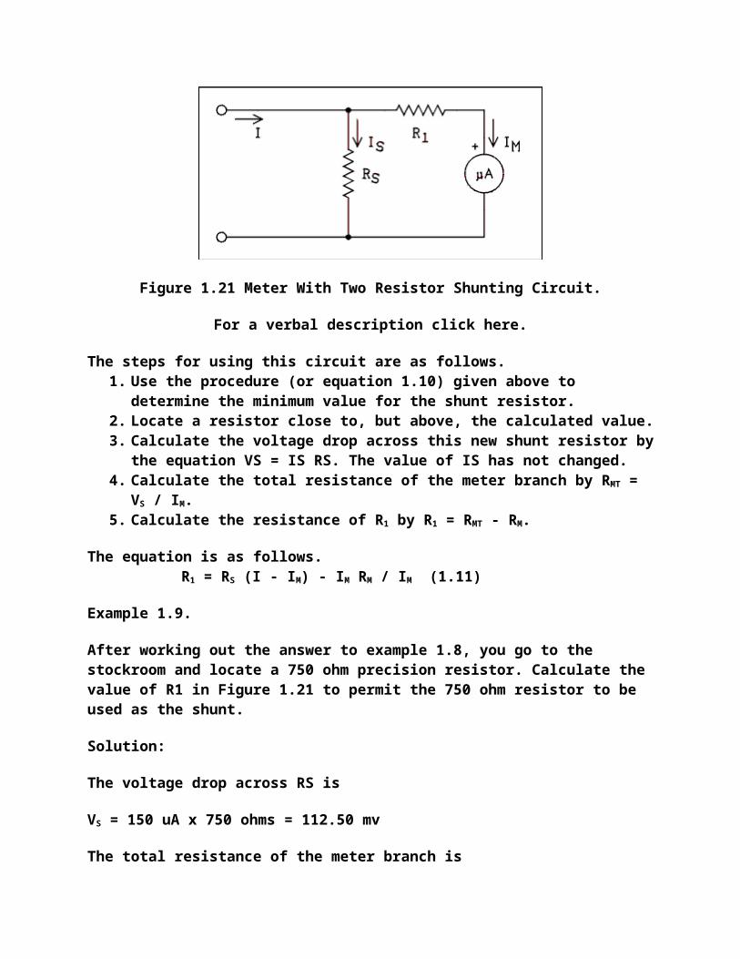
2.13 Problems.2.14 Answers to Problems.
Chapter 2.AC Circuits.
To date, we have dealt with sources of electrical energy which deliver direct current. DC flows continuously in one direction. The electrical world in which we live is one of alternating current (AC). The current supplied by the electric utility, audio signals, radio and television signals are all AC.
2.1 Alternating Current.
Alternating current reverses its direction on a regular time schedule. The current flows for a certain period of time, then reverses and flows for the same amount of time and then reverses again. There is no net movement of electrons in a wire carrying AC; the electrons simply vibrate in place.
The Cycle.
A cycle is defined as follows. The current rises from zero to a positive maximum, falls back to zero and "rises" to a negative "maximum" and then returns to zero. This definition of a cycle applies to current or voltage. For a cycle of voltage simply substitute the word "voltage" for "current" in the above definition.
If we plot a number of cycles on a graph (with current on the Y axis and time on the X axis) the plot will resemble the waves on the surface of a body of water. It is not considered correct usage to call a cycle a wave but even people with many years of experience sometimes get careless. It is considered correct usage to use the term waveform when referring to the shape of the graph of a cycle.
Notice that the definition of a cycle says nothing about the shape of the rises and falls. The cycle shape or waveform which is most often encountered is the sine wave. This waveform follows the sine function y = sin(x). Figure 2.1a shows two cycles of a sine wave alternating current. Figure 2.1b shows a square wave, 2.1c a triangular wave and 2.1d a sawtooth wave. There are an infinite number of different waveforms. The shape depends on what is generating them and what their use will be.
Figure 2.1 Four Different Waveforms.
For a verbal description click here.
Period and Frequency.
The period of an alternating current is the time required to complete one cycle. The frequency of an alternating current is the number of cycles which occur each second. The period is measured in units of time such as seconds, milliseconds or microseconds. The frequency has units of cycles/second or 1/time (a cycle is not a true unit, it is considered to be dimensionless.) The unit of frequency is called the hertz. Frequency may be given in hertz, kilohertz, megahertz or gigahertz.
The relationship between period and frequency is
(2.1) P = 1 / f
where P is the period in seconds and f is the frequency in hertz.
Example 2.1.
What is the period of the 60 hertz line frequency?
Solution:
P = 1/f = 1/60 = 1.67 x 10⁻² seconds or 16.7 ms.
Wavelength and Frequency.
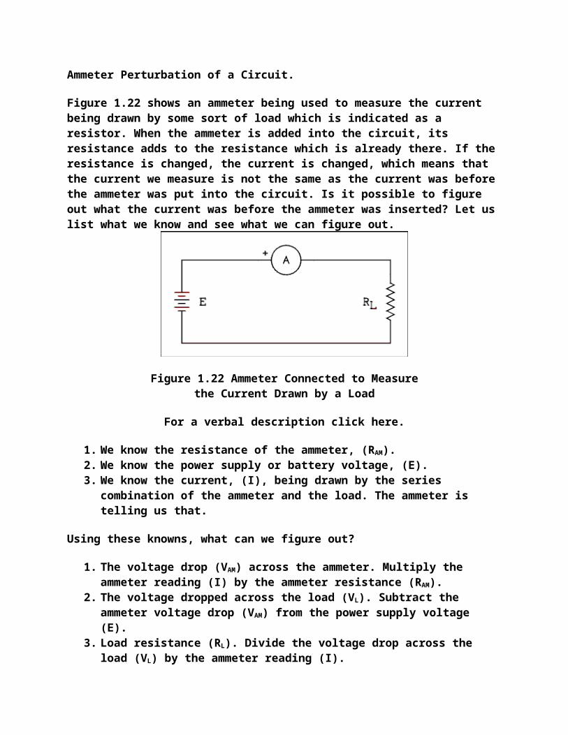
The only time that the term "wave" may be applied to an alternating current is when the current has been converted into a periodic disturbance which propagates through some medium. For example a loudspeaker converts AC of appropriate frequency into sound waves which propagate through the air. For another example, if AC of an appropriate frequency flows in a structure known as an antenna, electromagnetic waves will be radiated which will propagate through air, or the vacuum of space.
When waves propagate through a physical medium, the wave has a physical length. The wavelength is given by
(2.2) lambda = v / f where lambda is the wavelength in meters, v is the velocity of propagation in meters per second and f is the frequency in hertz. The speed of sound in air is approximately 335 meters per second and the speed of electromagnetic waves is 3 x 10⁸ meters per second.
Example 2.2.
A sound wave in air has a wavelength of 12 cm. What is its frequency?
Solution:
Using the speed of sound we have that
f = 335 / 0.12 = 2790 Hz.
Example 2.3.
A radio station is transmitting on a frequency of 88.9 MHz (megahertz). What is the wavelength of the electro- magnetic wave being transmitted?
Solution:
Using the speed of light we have
lambda = 3 x 10⁸ / 88.9 x 106 = 3.37 m
Angular Frequency.
When working through calculations involving AC it is often necessary for the frequency to appear in the argument of a sine or cosine function. A particular point on a waveform can be found by multiplying the frequency by the amount of time which has passed since the waveform has started. This would be all right if cycles were the only thing we had to deal with. The arguments of sines and cosines must be in angles, not in cycles.
One cycle consists of 360 degrees or 2 pi radians. The symbol for the angular frequency is usually a small omega but we will use a "w". The angular frequency is given by
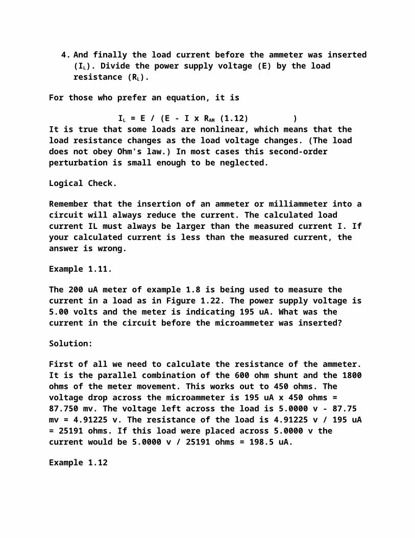
(2.3) w = 2 pi f where w is the angular frequency in radians per second and f is the frequency in hertz (cycles per second). A current can be expressed by the equation
(2.4) i = I sin( 2 pi f t ) where i is the current at any instant of time, I is the peak current, f is the frequency of the current in hertz and t is time in seconds. If f = 1 hertz then during the passage of one second the argument of the sine function will run through 2 pi radians and the sine function will execute one cycle in accordance with the definition of a cycle given above.
Magnitude Measurement of AC.
An alternating current may be represented by equation 2.4. The peak value of the current is "I" and the peak-to- peak value is 2I. The peak and peak-to-peak values are the most obvious and easiest to measure, which is probably why they are not the most often used.
The most useful measure of AC is a value which gives the same power dissipation in a resistor as a direct current. Suppose that a DC current of 3 amperes is flowing through a 1 ohm resistor. The power will be 9 watts. If an AC current of 3 amperes peak flows through a 1 ohm resistor, the power is not the same as for the DC. We require a measure which will give the same power as a DC of the same magnitude.
Because we are discussing power, that is the key. Remember that power is given by
P = I2 (2.5) R When a resistor is being heated, the average power is what is affecting the heating. To find the measure of current we must square the current, average it over time and then take the square root. The last step is necessary so that the new measure will be proportional to the peak current, not to the square of the current. The new measure of current is called the root-mean-square which is abbreviated RMS.
The RMS value of a current is given by
Substituting equation 2.4 into equation 2.6 we have
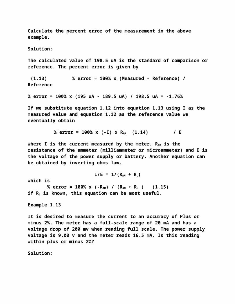
We don't know how to integrate the sine squared function but there is a way to change it to something we can integrate. We must make the trigonometric substitution
Sin2(t) = 1/2 ( 1 - cos( 2t )) Making this substitution and bringing I2 and 1/4 outside of the radical gives
The integral of the cosine over an integer number of cycles is zero; therefore,
The end result of all of this is
This is another one of those things you must remember. Conversions between RMS and peak, RMS and peak-to-peak, and peak and peak-to-peak are routine in electronics. The conversion applies to voltage as well as current.
Example 2.4.
Convert a peak current of 3 amperes to RMS.
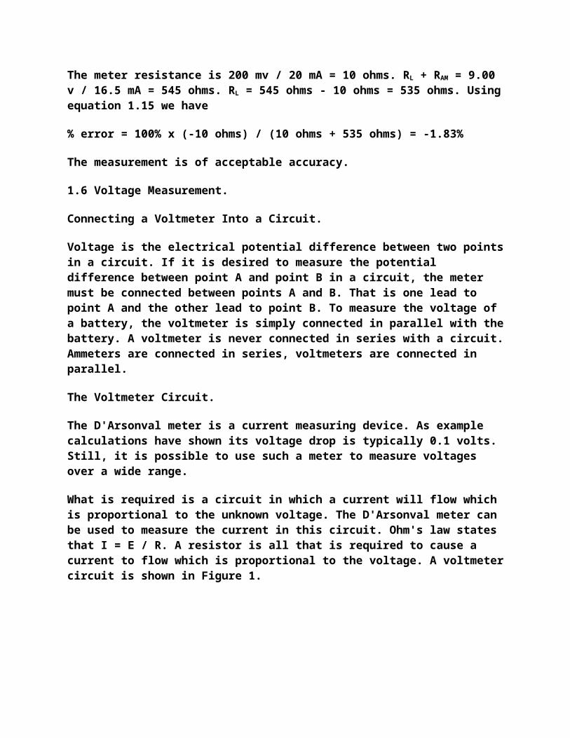
Solution:
IRMS = I / square root of 2 = 3 / 1.4142 = 2.12 A
Example 2.5.
Convert 6.3 v RMS to peak.
Solution:
VP = VRMS x square root of 2 = 6.3 x 1.4142 = 8.91 v The use of the RMS measure is so common in AC measurement that all quantities are RMS unless otherwise specified. If a specification gives a voltage as 117 vAC the meaning is 117 volts alternating current RMS (root-mean- square). The rule is: a voltage or current is RMS unless otherwise noted.
Logical Check.
The RMS value is always less than the peak value. RMS is a kind of average and an average will ALWAYS be less than the maximum. Similarly, the peak to peak value is greater than the peak value.
The Average.
One more AC measurement is worth mentioning. It is the average value. If an AC flows through a D'Arsonval meter movement the pointer will first be urged in one direction and then in the other. Most AC is of such a frequency that the meter's pointer cannot respond to either urging and the pointer does not move. If a rectifier is used to take the absolute value of the sine function, the meter will be able to respond to the unidirectional current in spite of the fact that it is changing with time. The meter will respond to, and indicate, the average value of the sine wave current.
If we averaged the sine function over one full cycle we would get zero. To obtain the average value of the absolute value of the sine it is sufficient to average it over one- half cycle.
A few turns of the crank gives IAV (2.9) = I x 0.63662
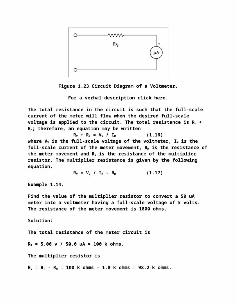
Most AC meters respond to average but are calibrated in terms of RMS. These meters work fine as long as the current or voltage being measured is a sine wave. If the input is not a sine wave the meter will not read the RMS but will read the average value times 0.70711 / 0.63662.
Use and Misuse.
The term AC is often used in ways which seem to be redundant or even contradictory. For example you might read "... the AC current ..." or "... the AC voltage ..." or even "... the AC power ...". Remember that the letters AC stand for alternating current. The first example is redundant, "alternating current current". The next two are contradictory. In spite of the redundant or contradictory nature of these terms they are used by most electrical and electronics engineers and technicians. The usage is too pervasive to be avoided even in formal writing. The writer will not make a rigorous attempt to exclude these terms from this book.
2.2 Capacitive Reactance.
Early researchers in electricity may have been surprised to find that AC would flow through a capacitor. After all, a capacitor is an open circuit, isn't it? Experiments on capacitors show that as more AC voltage is applied more current will flow. If the frequency is increased without changing the voltage the current will increase. It can also be shown experimentally that the current in a capacitor leads the voltage by 90 degrees or 1/4 of a cycle. The way in which a capacitor reacts to AC is called the capacitive reactance.
Let us apply a voltage to a capacitor and see what happens. The voltage is v = V sin( 2 pi f t ). We will use equation 0.41 which is restated here as equation 2.10.
(2.10) i = C dv / dt If we insert our definition of voltage into equation 2.10 we have
i = CV d / dt sin ( 2 pi f t ) Performing the differentiation gives.
i = C V 2 pi f cos( 2 pi f t ) If we say that the current is i = I cos( 2 pi f t ) we have that
I = C V 2 pi f solving for V/I gives.
V / I = 1 / ( 2 pi f C ) If you are awake you will recognize V / I as having the units of ohms. We now have a new quantity which in some ways is like resistance but in other ways is unlike resistance. We call this quantity the capacitive reactance and give it the symbol XC.
XC (2.11) = 1 / ( 2 pi f C ) where XC is the capacitive reactance in ohms, f is the frequency in hertz and C is the capacitance in farads.
We applied a sine wave voltage and a cosine wave current resulted. The cosine leads the sine by 90 degrees and so the current in a capacitor leads the voltage by 90 degrees.
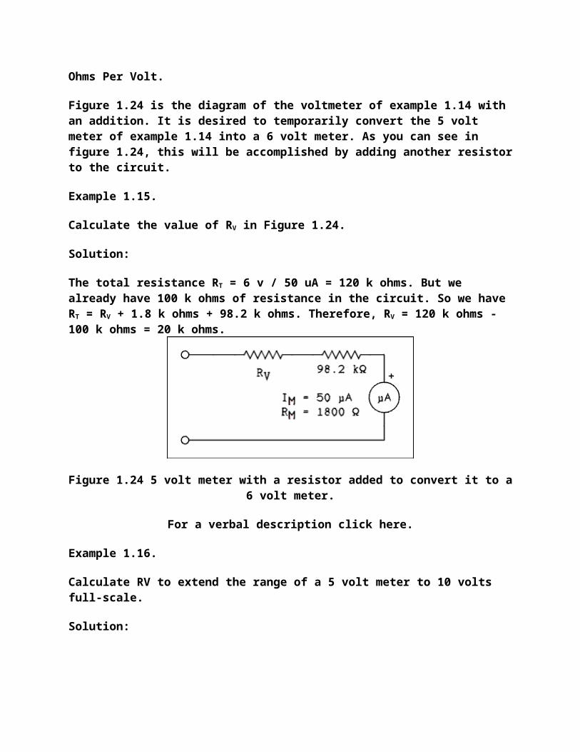
Example 2.6.
At what frequency will a .0039 uf capacitor have a reactance of 33 k ohms?
Solution:
Solving equation 2.11 for f gives
F = 1 / ( 2 pi XC C)
f = 1 / ( 2 pi x 3.3 x 104 ohms x 3.9 x 10⁻⁹ f ) =1.24 x 10³ Hz.
Example 2.7.
If a 0.1 uf capacitor is connected across the 120 vAC 60 Hz power line, how much current will flow?
Solution:
The reactance of a 0.1 uf capacitor at a frequency of 60 Hz is XC = 1 / ( 2 pi f C )
XC = 1 / ( 2 pi x 60 Hz x 1 x 10-7 f ) = 2.653 x 10⁴ ohms.
I = E / XC = 120 v / 2.653 x 10⁴ ohms = 4.52 x 10⁻³ A.
Power.
When an AC voltage is applied to a resistor, the current is in phase with the voltage. The instantaneous power is
p = (V sin( 2 pi f t ) ) x (I sin( 2 pi f t ) which is equal to
P = V x I x sin2( 2 pi f t ). By trigonometric substitution the sine squared function becomes a double frequency negative cosine function.
P = V x I x 1/2 (1 - cos( 2 pi 2 f t )). This function is entirely positive. When AC is applied to a resistor the power is "real". All energy flows from the generator into the load.
When an AC voltage is applied to a capacitor, the current leads the voltage by 90 degrees. The instantaneous power is
p = (V sin( 2 pi f t ) ) x (I cos( 2 pi f t ). Making the substitution for sine times cosine gives.
P = V x I x sin( 2 pi 2 f t )
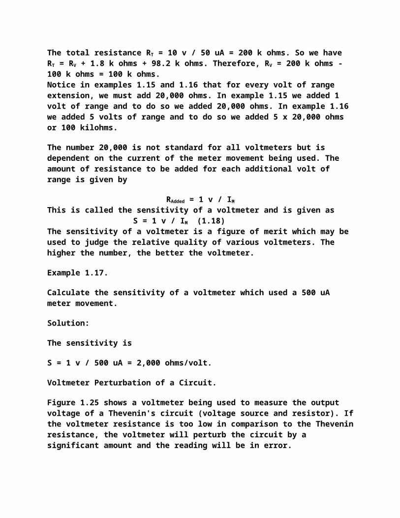
The sine times the cosine is a double frequency sine which has equal parts above and below the horizontal axis. This means that power is taken from the circuit for half of the time and given back for the other half of the time. The net value of power averaged over time is zero.
Here we have an incongruous situation. There is a voltage applied to a circuit element (capacitor) and there is a current flowing but the power is zero! This can be verified experimentally. It must have been "mind blowing" for the first person (probably a graduate student) who observed it.
2.3 Inductive Reactance.
Early researchers in electricity must have been surprised to find that a coil of wire presented more "resistance" to the flow of alternating current than did the identical length of wire which was not wound into a coil. Experiments on inductors show that as more AC voltage is applied more current will flow. If the frequency is increased without changing the voltage the current will decrease. It can also be shown experimentally that the current in an inductor lags the voltage by 90 degrees or 1/4 of a cycle. The way in which an inductor reacts to AC is called the inductive reactance.
Let us apply a current to an inductor and see what happens. The current is i = I sin( 2 pi ft ). We will use equation 0.55 which is restated here as equation 2.12.
(2.12) e = L di / dt If we insert our definition of current into equation 2.12 we have
e = L V d/dt sin(2 pi f t ) Taking the derivative gives.
e = L V 2 pi f cos( 2 pi ft ) If we say that the voltage is e = E cos( 2 pi ft ) we have that
E = L I 2 pi f solving for E gives
E / I = 2 pi f L If you are awake you will recognize E / I as having the units of ohms. We now have a new quantity which in some ways is like resistance but in other ways is unlike resistance. We call this quantity the inductive reactance and give it the symbol XL.
XL (2.13) = 2 pi f L where XL is the inductive reactance in ohms, f is the frequency in hertz and L is the inductance in henrys.
We applied a sine wave current and a cosine wave voltage resulted. The cosine leads the sine by 90 degrees and so the voltage in an inductor leads the current by 90 degrees.
Example 2.8.
What is the value of an inductor which will present a reactance of 47 k ohms at a frequency of 100 kHz?
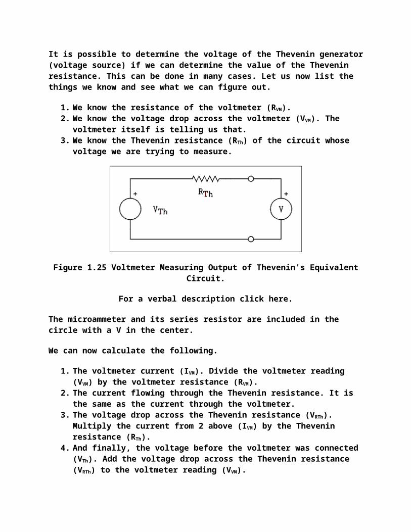
Solution:
Solving equation 2.13 for L we have
L = XL / ( 2 pi f )
L = 47 k ohms / ( 2 pi 100 kHz ) = 7.48 x 10⁻² H or 74.8 mH
Example 2.9.
If a 500 uH inductor is used in a power line filter, how much voltage drop will be introduced at a current of 25 amperes?
Solution:
The power line frequency in the U.S. is 60 Hz. XL = 2 pi f L
XL = 2 pi x 60 Hz x 500 uH = 0.1885 ohms
The voltage drop is I x XL = 25 A x 0.1885 ohms = 4.71 v
The power in a pure inductance is zero by the same argument as for capacitors. It makes no difference that the current is lagging instead of leading. The phase difference is still 90 degrees.
2.4 Series Circuits and Impedance.
DC circuit analysis contains only resistors and DC sources. Most real circuits operate using AC and employ capacitors and inductors. Because we must be capable of analyzing AC circuits as well as DC circuits we must study some new techniques. In this section we will develop some simple tools for the analysis of series AC circuits.
Series RC Circuits.
Figure 2.2 Series RC Circuit Driven by an AC Generator.
For a verbal description click here.
Figure 2.2 is the diagram of a simple RC circuit which contains an AC generator. The generator can take on any output voltage and any frequency.
Kirchhoff's law tells us that the current everywhere in the circuit will have the same magnitude. An extension of this law to AC circuits is to add phase. The current everywhere in the circuit will have the same phase. The current in the generator, the current in the resistor and the current in the capacitor are all in phase with each other.
The voltage across the resistor will be in-phase with the current through it. Resistors do not play tricks on us; they obey Ohm's law. The voltage and current in a resistor are always in-phase with each other.
The phase relationship between the voltage and current in a capacitor is 90 degrees with the current leading. If the current leads, the voltage follows or lags. In this example we are using the current as a reference so we say the voltage is lagging the current by 90 degrees. This can be represented pictorially as in Figure 2.3.
In Figure 2.3 the voltages and currents are represented by line segments in a plane. These lines have length and direction. Some texts refer to these as vectors. Vectors have magnitude and direction in real space and are (or at least can be) three-dimensional. The lines which represent voltages and currents cannot be three-dimensional; they are strictly two-dimensional. In addition to this, the directions do not represent directions in space, they represent relative phases of voltages and currents in electric circuits. For all of these reasons, the lines are called phasors. It should be noted that this term has been in common use in electrical engineering texts and by electrical engineers for a long time and predates the television show "Star Trek" by several decades.
Figure 2.3 Phase Relationships of Voltages and Currents.
For a verbal description click here.
Figure 2.4a is the diagram of an R-L circuit. The phasor diagram for this circuit is shown in Figure 2.4b. In an inductor the voltage leads the current by 90 degrees and so the voltage phasor is shown pointing upward. As always the voltage and current are in-phase in a resistor.
Figure 2.4 (a) R-L Circuit and (b) Its Phasor Diagram.
For a verbal description click here.
Kirchhoff's law tells us that the voltage of the generator in Figure 2.2 is the sum of the voltage across the resistor and the voltage across the capacitor. These voltages are not in phase and they cannot be added simply by adding their magnitudes. Their directions must also be taken into account. Even though we do not call them vectors the techniques of vector addition apply. As vector addition should be well known to any student studying physics, we will not dwell on the addition of vectors (phasors).
The fact that these phasors are at right angles makes life a lot easier for us. The familiar Kirchhoff's equation for voltages looks like this for AC:
where VG is the generator voltage, VR is the voltage across the resistor and VC is the voltage drop across the capacitor.
The phase angle theta of the generator voltage is given by
theta = arctan ( VC / VR (2.15) ) To obtain the correct sign on the angle you must attach a minus sign to VC and a plus sign to VL.

Figure 2.5 R-LC (a Circuit and (b> Its Phasor Diagram.
For a verbal description click here.
If we now combine resistance, capacitance and inductance in the same circuit, as in Figure 2.5a, the phasor diagram of Figure 2.5b will result. Since VL and VC are 180 degrees apart, one will always subtract. The phasor version of Kirchhoff's voltage equation is as follows.
The phase angle is given by Theta = arctan ( ( VL - VC ) / VR (2.17)
Example 2.10.
In Figure 2.2 the magnitudes of the voltages are as follows. VR = 77.460 v at 0 degrees and VC = 91.652 v at -90 degrees. What are the magnitude and phase of the generator voltage?
Solution:
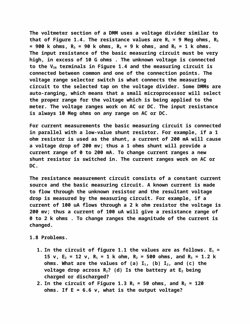
The phase angle is
theta = arctan ( -91.652 v / 77.460 = 49.80 degrees.
Ohm's Law For AC.
When we made the change from DC to AC we did not repeal Ohm's law. Its form is just a little different. For resistors it is unchanged.
VR (2.18) = I R For capacitors and inductors it is as follows.
VC = I XC and VL = I XL (2.19) For a series combination of RC or R-L we will call the "resistance" something different.
VG (2.20) = I Z The quantity Z is called impedance and is the ratio of the generator voltage to the generator current. The impedance like the generator voltage has magnitude and angle. It is a phasor.
We can get equations for the magnitude and angle of the impedance by substituting equations 2.18, 2.19 and 2.20 into equations 2.16 and 2.17. Because the current is the same everywhere in the circuit it will cancel out and leave us with these equations. The magnitude is
The phase angle is given by theta = arctan ((XL - XC (2.22) ) / R
Impedance magnitude and phase angle involve reactances which are frequency dependent. An impedance can be calculated only if the frequency is fixed and known. If the frequency is changed, the impedance must be recalculated.
Example 2.11.
In Figure 2.2 R = 1 k ohms, C = 0.1 uf and f = 1 kHz, what is the impedance?
Solution:
First, XC must be determined.
XC = 1 / ( 2 pi 1000 x 0.1 x 10-6 ) = 1592 ohms
The magnitude of the impedance is
The phase angle is
theta = arctan (-1592 ohms / 1000 ohms) = -57.87 degrees.
The accepted way of writing this is
Z = 1880 ohms / -57.87 degrees
which is spoken as "1880 ohms at an angle of -57.87 degrees".
Back to Fun with Transistors.Back to Fun with Tubes.Back to Table of Contents.Back to top.
2.5 RC Filter Circuits.
One of the most commonly encountered applications of a series RC circuit is a filter. Filters are used to filter out an unwanted band of frequencies which may coexist with a wanted band of frequencies. An example is the output voltage of a thermocouple which is being used to measure the temperature in a crystal-growing oven. The temperature in the oven will change very slowly and the wanted data are contained on a voltage which is changing very slowly. The frequency content will be from zero frequency (DC) to about 0.1 Hz. An unwanted frequency which is extremely likely to be present is the ubiquitous and omnipresent 60 Hz power line frequency. A filter can be designed which will reduce magnitude of the 60 Hz output to a very low level without appreciably affecting the magnitude of the 0 to 0.1 Hz data signal.
Notice that word which is boldfaced above. A filter never removes an unwanted signal. There is no such thing as "remove". It's the same thing as taking a step equal to half of the distance to the wall. You can get as close to the wall as you want but you never can get there. A filter can be constructed to reduce an unwanted signal to as low an amplitude as desired but you never will be able to construct a filter to get the amplitude to zero.
Figure 2.6 Frequency Response of a Low-pass Filter.
For a verbal description click here.
Figure 2.7 Frequency Response of a High-pass Filter.
For a verbal description click here.
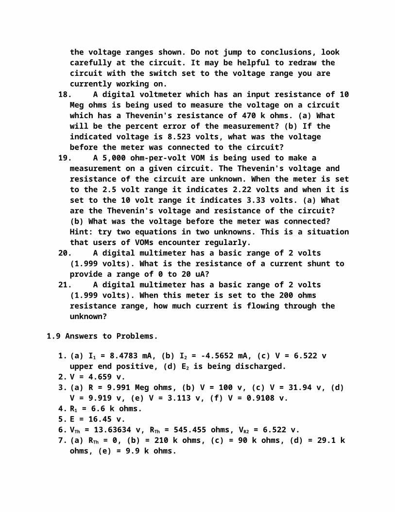
Filters can be divided into two groups, low-pass and high-pass. A low-pass filter will pass low frequencies and attenuate high frequencies. A high-pass filter will pass high frequencies and attenuate low frequencies. The dividing line between high and low is called the cutoff frequency.
The term "cutoff frequency" gives a false impression about how filters work. The notion is that all frequencies on the "pass" side of the cutoff frequencies are passed and all frequencies on the other side of the cutoff frequency are removed. That impression is wrong! The cutoff frequency is defined as that frequency where the output power is down to half of the input power. Figure 2.6 shows how the output of a low-pass filter which has a cutoff frequency of 1000 Hz (1 kHz) varies with frequency. Figure 2.7 shows the frequency response of a high-pass filter which also has a cutoff frequency of 1 kHz.
Do not be concerned if you don't know what a dB is. For now all you need to know is that it is a logarithmic function of VO / VI. The dB will be explained fully in section 2.6.
You will notice in Figures 2.6 and 2.7 that each filter has a portion of its frequency response curve where the output is unchanged as frequency changes. This is called the "flat" portion of the frequency response. The portion where the output is changing with frequency is called the "roll off" part of the curve. The cutoff frequency is that frequency where the output power is down to 1/2 of the power in the flat part of the curve. That does not conflict with the statement above because (in most cases) in the flat part of the curve the output power is equal to the input power.
Using the equation P = V2 / R it can be shown that when the power is reduced by 1/2 the voltage is reduced by 0.7071 which is 1 over the square root of 2. At the frequency where XC = R the output voltage is 0.7071 of the input voltage. This will be illustrated in an example. Thus the cutoff frequency is where XC = R.
Separating AC and DC.
As you will learn in later chapters, signals in electronics are often mixtures of AC and DC. In many cases it is desired to remove one or the other. A signal may have the form
v = VDC + VP (2.23) sin( 2 pi f t ) where VDC is the DC part of the signal, VP is the peak value of the AC part of the signal and f is the frequency of the AC part of the signal. Figure 2.8a shows an equivalent circuit of a DC + AC generator. Figure 2.8b is a graph of the output voltage versus time.
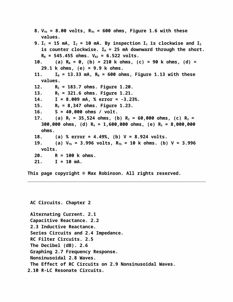
Figure 2.8 DC + AC Generator (a) and Its Output (b).
For a verbal description click here.
Figure 2.9 Low-pass Filter with Its Input and Output.
For a verbal description Click here.
Suppose we pass this DC + AC signal through a low-pass filter as in Figure 2.9. The frequency of the AC is much higher than the cutoff frequency of the filter. That is equivalent to saying that XC is much less than R at the frequency of the AC generator. Most of the AC will be shorted out by the capacitor but the DC will be unaffected. Consequently the AC will be attenuated while the DC will not.
Figure 2.10 High-pass Filter With Its Input and Output.
For a verbal description click here.
Now let us pass this DC + AC signal through a high-pass filter as in Figure 2.10. The frequency of the AC is much higher than the cutoff frequency of the filter. That is equivalent to saying that XC is much less than R at the frequency of the AC generator. The AC will be affected very slightly by the filter but the DC will be totally removed.
Consequently the DC will be attenuated while the AC will not. Because DC is zero frequency, absolutes do apply. The magnitude of the DC will be reduced to zero.
Attenuation of Unwanted AC Signals.
It is easy to calculate the amount of attenuation a filter will introduce at any frequency. The procedure is quite similar to that used to solve a voltage divider in DC circuits.
1. Calculate the capacitive reactance XC and then the circuit impedance Z. 2. Calculate the circuit current using the known or an assumed input voltage and the
total circuit impedance Z. 3. Multiply the current by the resistance or the reactance of the element across which
the output is taken. 4. Determine the attenuation ratio by dividing the calculated output voltage by the
known or assumed input voltage.
For those who would prefer equations they are.
For a low pass filter.
For a high pass filter.
Calculation of phase angle is usually not necessary.
Example 2.12.
In Figure 2.9, R = 1 k ohms and C = 10 uf. What is the attenuation ratio at a frequency of 60 Hz? Solution: First, calculate the reactance of the capacitor at 60 Hz.
XC = 1/(2 pi f C) = 1/(2 pi 60 Hz x 10 x 10-6 f) = 265.26 ohms.
The circuit impedance is
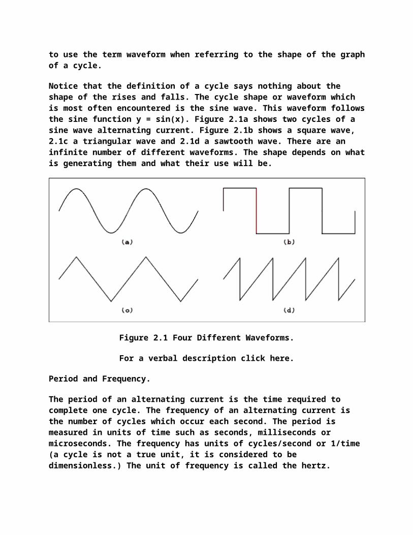
Assume an input voltage of 1 v and calculate I = E / Z
I = 1 v / 1034.58 ohms = 9.6658 x 10⁻⁴ A.
VO = I XC = 9.6658 x 10-4 A x 265.26 ohms = 0.256 v. Dividing this output voltage by 1 v gives the attenuation ratio of 0.256.
Example 2.13.
In the circuit of Figure 2.10 R = 1592 ohms and C = 0.1 uf. What are the attenuation ratios at (a) 60 Hz and (b) 1 kHz?
Solution:
For details on the calculations of XC, Z and I you are referred to example 2.12. Calculating XC at 60 Hz and 1 kHz we haveXC at 60 Hz = 2.653 x 10⁴ ohms andXC at 1000 Hz = 1592 ohms.Calculating the circuit impedance at 60 and 1000 Hz.Z at 60 Hz = 2.658 x 10⁴ ohms andZ at 1000 Hz = 2251 ohms.The current for 1 v input is found to beI at 60 Hz = 3.762 x 10⁻⁵ A andI at 1000 Hz = 4.442 x 10⁻⁴ A.All that remains is to calculate the output voltage. This is the only part of this example which is different from example 2.12. For Figure 2.10 the output voltage is (a) VO = I R.At 60 Hz VO = 3.762 x 10-5 A x 1592 ohms = 5.99 x 10⁻²v.The attenuation ratio AR = 5.99 x 10⁻²
(b) At 1000 Hz VO = 4.442 x 10-4 A x 1592 ohms = 0.707 vtherefore AR = 0.707
In the above examples we have defined the attenuation ratio of a filter to be
AR = VO / VI (2.24) where VO is the output voltage of the filter at one particular frequency and VI is the input voltage at the same frequency. The output divided by the input is often called the "gain" of the circuit. The term gain implies an increase, not a decrease as occurs in a passive circuit.
The term gain will make more sense when we study amplifiers which do increase the amplitude of the input signal.
In the examples above if the attenuation is desired at several different frequencies it would be necessary to recalculate the value of XC for each frequency. There is a way to avoid these repeated calculations. Let us write a general equation for the attenuation ratio of a low-pass filter and see what we can do with it. The general equation is this.
Now we will make the substitution XC = 1 / (2 Pi f C).
Now we will multiply the above equation through by 2 Pi f C to obtain.
The cut-off frequency is where XC = R. If we substitute into the reactance equation we have R = 1 / (2 Pi fC C)
Solving for the cut-off frequency gives. fC = 1 / (2 Pi R C).
We can substitute this into the above equation and obtain.
Where fc is the cut-off frequency and f is any given frequency.
If we start from the high pass filter equation and follow the same procedure we will obtain.
Either one of these equations may easily be solved for fc to find the cut-off frequency for a given frequency and attenuation or for f to find the frequency for a given attenuation for a given filter.
Logical Checks.
The output voltage of an RC filter will always be less than or equal to the input voltage. If you get an output which is larger than the input, you have made a mistake.
For a low-pass filter, the output will decrease as the frequency increases. If asked to calculate the attenuation ratio at two different frequencies and you get an answer which says that the higher frequency gives a larger output voltage than does the lower frequency, you have made a mistake.
For a high-pass filter, the output will increase as the frequency increases. If asked to calculate the attenuation ratio at two different frequencies and you get an answer which says that the lower frequency gives a larger output voltage than does the higher frequency, you have made a mistake.
Example 2.13.1.
In the circuit of Figure 2.10 R = 1592 ohms and C = 0.1 uf. What are the attenuation ratios at (a) 60 Hz and (b) 1 kHz?
Solution:
This is a repeat of Example 2.13. Lets try the new tools we have. First of all.
fC = 1 / (2 Pi R C) = 1 / (2 Pi 1592 x 0.1 x 10-6) = 1000 Hz.
From equation 2.24.5 we have.
AR = 1 / sqrt(1 + (fC/f)2)
(a) AR = 1 / sqrt(1 + (1000/60)2) = 0.0599
(b) AR = 1 / sqrt(1 + (1000/1000)2) = 0.707
Example 2.13.2.
A low-pass filter is needed that has an attenuation ratio of 1.8 x 10⁻³ at a frequency of 60 Hz. (a) What is the cut-off frequency of this filter? (b) If the resistor is 1 Meg ohm what is the capacitor value?
Solution:
Solving equation 2.24.4 for fc gives.
(a) Fc = 60 x 1.8 x 10-3 / sqrt(1 - (1.8 x 10⁻³)2) = 0.108 Hz.
(b) C = 1 ( 2 Pi fc R) = 1 / (2 Pi 0.108 x 106 = 1.47 uf.
Example 2.13.3.
A high-pass filter must have an attenuation of 0.966 at a frequency of 20 Hz. (a) What is the cut-off frequency, and (b) What is the capacitor if the resistor is 470 k ohms?
Solution:
Solving equation 2.24.5 for fc gives.
(a) fc = sqrt(1 - 0.9662) / (20 x 0.966) = 5.35 Hz.
(b) C = 1 / (2 Pi 5.35 x 470 x 103) = 0.0633 uf.
2.6 The Decibel (dB).
The decibel (dB) is one tenth of a Bell (B), as in Alexander Graham Bell. From this you might assume that the Bell and decibel have something to do with sound and you would be partly correct.
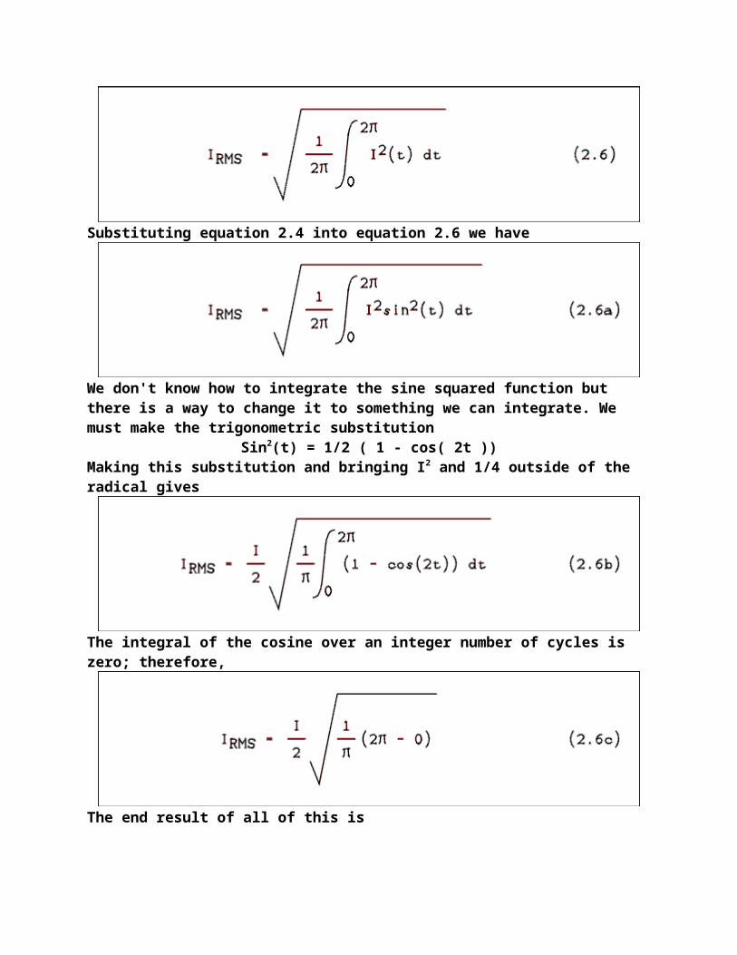
The dB began life as a measure of sound pressure level. A dB is the smallest change in sound level which the human ear can detect. The key to understanding the dB is that word "change". There is no absolute zero on the dB scale.
Because the telephone converts sound to an electrical signal, an electrical definition of the dB is closely tied to the sound level definition. The electrical definition is
dB = 20 Log ( V2 / V1 (2.25) ) or
dB = 10 Log ( P2 / P1 (2.26) ) where P1 and P2 are powers and V1 and V2 are voltages. The quantity which is subscripted 2 is the one to be expressed in dB and the quantity which is subscripted 1 is the chosen reference. For example the gain of an amplifier or loss (attenuation) of a filter can be expressed in dB as follows.
dB = 20 Log (VO / VI (2.27) ) Where VI is the input voltage and VO is the output voltage. In the above equations, if V2 = V1, P2 = P1 or VO = VI, the result is zero (0) dB. The denominator of the argument of the log function is called the reference level because it determines where the zero on the dB scale will be placed.
The reference level may be anything which the occasion demands. There are far too many standard references to list here but there is one which is so common that it is worth mentioning. A standard reference is 1 milliwatt in 600 ohms. The voltage is V2 = P R = 1 x 10-3 w x 600 ohms = 0.60 square volts and V = 0.7746 v. This dB scale is referred to as the dBm (dB referred to 1 milliwatt) scale and it appears on most analog AC meters. It is also known as the VU (volume unit) scale. The VU meters in a tape deck or radio station console use this scale.
The dB is widely used because its logarithmic nature permits it to express a wide range of values in a compact form. It is most useful in graphing quantities which have a wide range. This will become apparent in the next section.
Example 2.14.
Express the following power levels in dBm: (a) 25 microwatts, (b) 1 milliwatt, (c) 1 watt and (d) 75 watts.
Solution:
(2.28) dBm = 10 Log P / 1 mw
(a) -16.0 dBm, (b) 0 dBm, (c) 30 dBm and (d) 48.8 dBm.
Example 2.15.
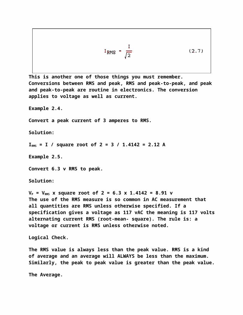
Express the following voltage levels in dBm: (a) 5 microvolts, (b) 2 millivolts, (c) 6 volts and (d) 120 volts.
Solution:
(2.29) dBm = 20 Log V / 0.7746 v
(a) -103.8 dBm, (b) -51.8 dBm, (c) 17.8 dBm and (d) 43.8 dBm.
Example 2.16.
A filter is being operated at its cutoff frequency. (a) Use power to express the attenuation ratio in dB. (b) Use voltage to express the attenuation ratio AR in dB.
Solution:
At the cutoff frequency the output power is 1/2 of the input power and the output voltage is 0.7071 of the input voltage. (a) dB = 10 Log 0.5 = -3.01 dB. (b) dB = 20 Log 0.7071 = -3.01 dB. Let's call them both -3 dB.
At the cutoff frequency the filter's output is 3 dB down from its flat response output level. The cutoff frequency is often called the "3 dB point" or the "half-power point".
Example 2.17.
Express the results of examples 2.12 and 2.13 in dB.
Solution:
The result of example 2.12 is AR = 0.256. Since AR = VO / VI we have dB = 20 Log AR = 20 Log 0.256 = -11.8 dB.
The results of example 2.13 are at 60 Hz AR = 5.99 x 10⁻² and at 1000 Hz AR = 0.707. At 60 Hz ARdB = -24.4 dB and at 1000 Hz ARdB = -3 dB.
Example 2.18
In the frequency response curve of Figure 2.6 the attenuation at 1 MHz is 60 dB, at 100 kHz it is 40 dB, at 10 kHz it is 20 dB and at 1 kHz it is 3 dB. What is the value of AR at each of these frequencies?
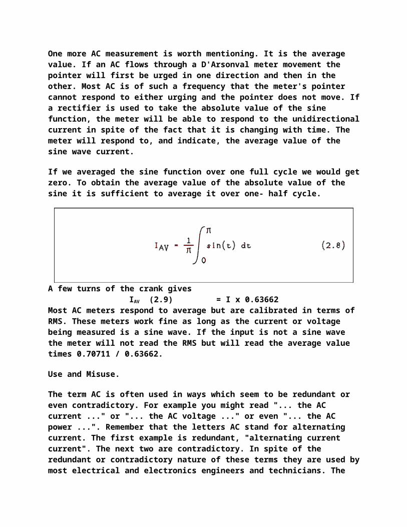
Solution:
Starting from the equation dB = 20 Log AR and taking the antilog of both sides we have
AR = 10dB/20.
At 1 MHz AR = 10-60/20 = 1 x 10⁻³, At 100 kHz AR = 10-2,at 10 kHz AR = 10-1, and at 1 kHz AR = 10-3/20 = 0.708, which shows that there are often errors in reading graphs.
2.7 Graphing Frequency Response.
As with most other things there is a right way and several wrong ways to graph frequency response curves. First we will discuss what makes a "good" graph in general and then show some examples of wrong ways to graph frequency response.
The best possible graph is a straight line. It is easy to draw, easy to pick off values from and easy to fit an equation to. If you can't get a single straight line, a couple of line segments joined by a short curving section is the next best thing. The graphs in Figures 2.6 and 2.7 fit the latter description nicely.
One of my professors once said, in jest I'm sure, "If you can get your data to plot as a straight line you should get your PhD on the spot, and if you can get the line to go through the origin you should get the Nobel prize."
In Figures 2.6 and 2.7 the frequency is plotted on a logarithmic scale. The distance between 1 and 10 is the same as the distance between 10 and 100, which is also the same as the distance between 100 and 1000. On a linear scale the distance between 10 and 100 would be 10 times larger than the distance between 1 and 10. The first dotted vertical line to the right of 1 is for 2. The next dotted line is for 5. The two dotted lines to the right of 10 are for 20 and 50 respectively. Other interpolation markings have been omitted to keep the graph from being too cluttered.
The vertical scale in Figures 2.6 and 2.7 is plotted in dB. Now that you know what a dB is you know that the vertical scale is also a logarithmic scale. If you think back to geometry you will remember that if you plot y = 1/x on a log-log scale it is a straight line. The roll-off portion of the graph of a low-pass filter is a 1/f curve, as shown in Figure 2.6. In Figure 2.7 the straight part of the roll-off is a simple y=x function which is a straight line on a log-log as well as a linear graph.
Some Wrong Ways.
Given a set of data and told to "go and plot it" with no further instructions the natural thing to do would be to use linear axes for both x and y coordinates. Figure 2.11 shows data for a low-pass filter which has been plotted on linear scales for frequency and attenuation
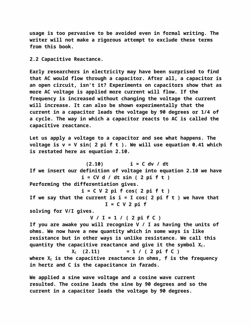
ratio. Note that we are not using dB but just the values of AR. Because the raw data goes from 1 hertz to 1 megahertz the frequency scale is from 0 to 1 megahertz. The attenuation scale is from 0 to 1.
As you can see from Figure 2.11 the frequency response curve is a shy little thing that attempts to hide behind the X and Y axes. It is not very useful because it would be impossible to pick values from except in a very small part of the curve.
Figure 2.11 Frequency Response of a Low-pass FilterPlotted on Linear Scales 0 to 1 MHz.
For a verbal description click here.
The curve can be pulled away from the edges by changing the scale. Figure 2.12 shows the same data plotted from 0 to 6 kilohertz. While this scale throws away most of the data it does make for a readable graph.
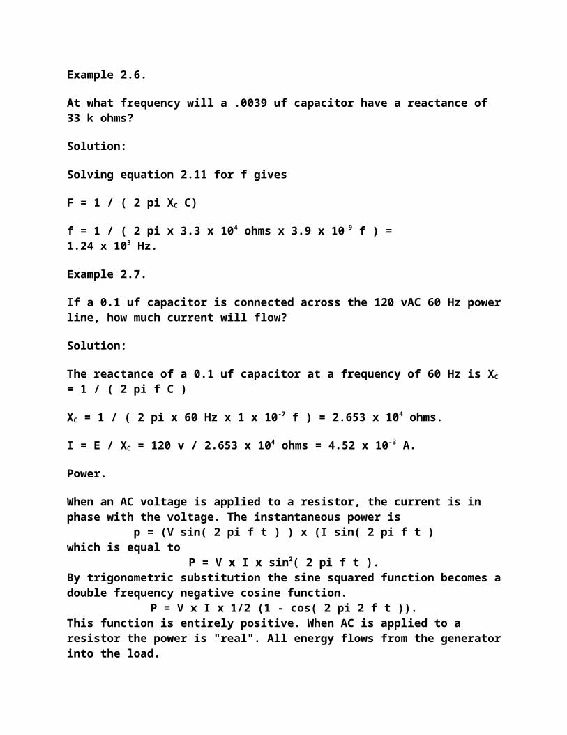
Figure 2.12 Frequency Response of a Low-pass FilterPlotted on Linear Scales 0 to 6 kHz.
For a verbal description click here.
What is needed is a scale which allows wider spacing of numeric intervals when the values are small and closer spacing when the values are large. That sounds like the description of a logarithmic scale. Figure 2.13 is getting better because the frequency is now on a log scale. The vertical axis is still the attenuation ratio which ranges from 0 to 1. It is a linear scale.
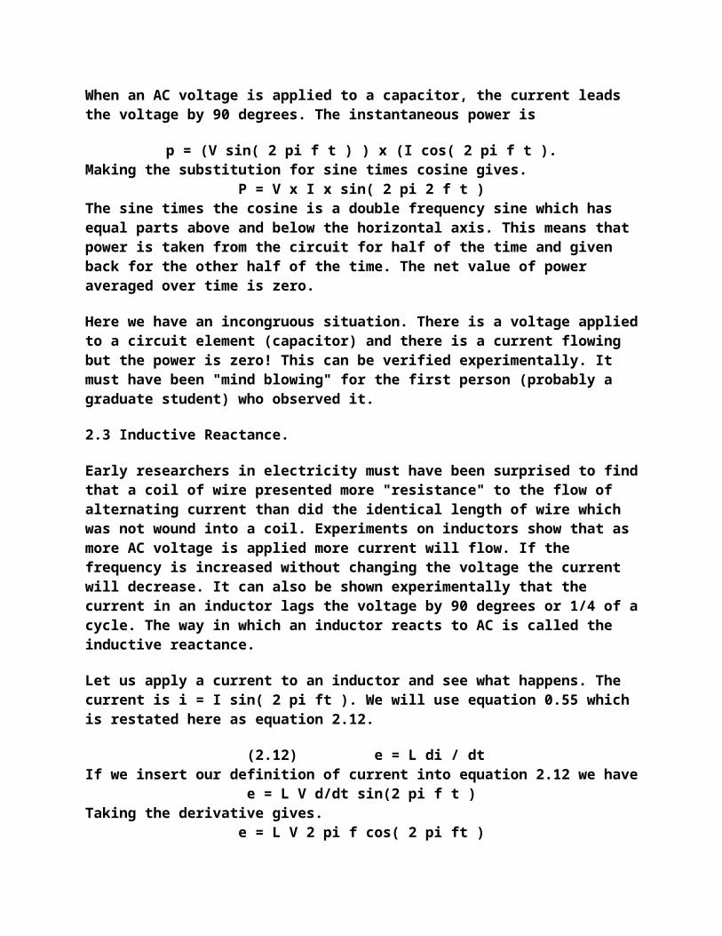
Figure 2.13 Frequency Response of a Low-pass FilterPlotted on Logarithmic Scales 1 Hz to 1 MHz.
For a verbal description click here.
From this figure it is possible to tell that the attenuation ratio is 0.707 at 1 kHz. Inspection of this graph indicates that the output of the filter is zero above 100 kHz. This is not the case! The output of a filter never goes to zero. We are in need of a logarithmic scale for the attenuation ratio as well as the frequency.
A log scale for the attenuation ratio could be obtained by using log-log graph paper to plot the data. Alternatively, we could simply take the log of AR but since the dB is so well known it seems to be the best way to get a log scale on the vertical axis. As all analog AC voltmeters have a dB scale the data may be taken in dB for plotting directly on a graph.
In Figure 2.6 we can see that the filter's output is down 3 dB at 1 kHz. We can also see that the output is down 20 dB at 10 kHz, 40 dB at 100 kHz and 60 dB and 1 MHz. In fact the output of a low-pass filter decreases by 20 dB for every decade increase in frequency. This particular rate of decrease is specific to a low-pass filter consisting of one capacitor and one resistor. Filters which are more complex will have roll-off rates of 40, 60, 80, and so on dB per decade of frequency.
Using Store-bought Graph Paper.
Many students become confused when they set out to plot a frequency response curve on a piece of semi-log graph paper. To begin with the numbers are printed on the paper in the wrong orientation. To read the numbers right-side-up you will hold the paper so that the log axis is vertical. As you can see in figure 2.6 the log axis is horizontal. Even after getting the paper turned the right way, there is still confusion about what to do with those numbers and how to relate them to frequency.
Semi-log and log-log graph paper is sold by cycles. One cycle will cover one decade of data. A representation of a piece of 2 cycle semi-log paper is shown in Figure 2.14. The numbers have been turned right-side-up for easier reading.
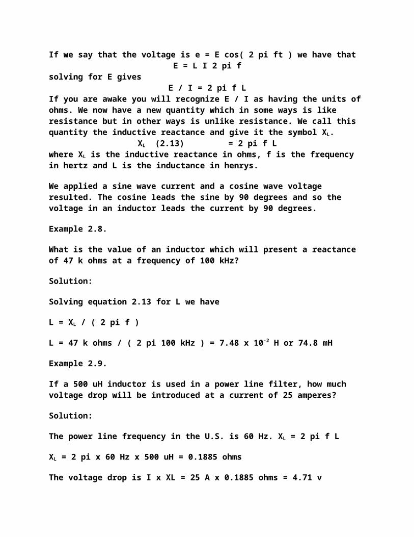
Figure 2.14 Representation of a Piece of Semi-log Graph Paper.
For a verbal description click here.
The numbers across the top are the numbers which are printed on the paper. The numbers in each successive decade are spaced a little farther out from the graph. The line between 1 and 2 is for 1.5. You may have noticed that it is not equidistant between 1 and 2. That is the nature of a log scale.
To plot frequency on this graph paper you would label the horizontal axis as shown along the bottom of the graph. If you have more decades to plot you must buy another piece of graph paper which has more cycles. When you go to the bookstore to buy semi-log or log-log paper you should know how many decades of data you have to plot.
If semi-log paper cannot be obtained in the desired number of cycles, it is possible to use linear paper and take the log of frequency. The log of frequency has no particular meaning (there is no equivalent to the dB for frequency), which makes it necessary to label the graph with frequency in hertz rather than log of frequency.
The magnitude (Y axis) of a frequency response plot may be plotted on a linear scale in dB or on a log scale in attenuation ratio. Although either way is acceptable, plotting dB on a linear scale is by far the most commonly used method.
2.8 Nonsinusoidal Waves.
As shown in Figure 2.1 there are waves other than sine waves. These other waves are made up of sine waves in combination.
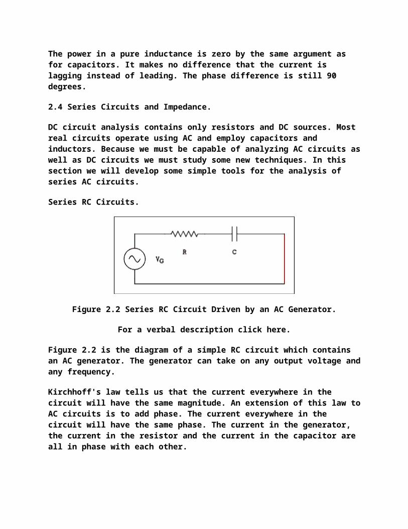
Sinusoids.
The simplest of oscillators, (devices which generate waves), produces a sine or cosine function. When the output of such an oscillator is plotted versus time, the result is what we call a sine wave. When a waveform is not sinusoidal (square, triangular or just not a sine wave), it can be shown mathematically and physically to be the sum of several sinusoidal waves.
Harmonics.
A harmonic is a frequency which is an integer multiple of another frequency. The "other" frequency is called the fundamental frequency. Thus a complex (nonsinusoidal) waveform is made up of a fundamental frequency, which is a sine wave with the largest amplitude and lowest frequency, and several other sine waves which are lower in amplitude and integer multiples of the fundamental frequency.
Numbering Harmonics.
Harmonic numbers are assigned on the basis of their relationship to the fundamental frequency. The fundamental frequency itself is the first harmonic. The frequency which is twice the fundamental frequency is called the second harmonic. The frequency which is three times the fundamental frequency is called the third harmonic and so on. The frequency of any harmonic is just the harmonic number multiplied by the fundamental frequency.
Fourier Series.
Remember the angular frequency? The symbol usually used for the angular frequency is a lower case omega. That symbol does not appear on my word processor. We will use instead a "w". If we call the nonsinusoidal wave F(wt) then the general form of the Fourier series for F(wt) is given by
F(wt) = a0 + a1 cos(wt) + a2 cos(2wt) + ... + an cos(nwt) + b 1 sin(wt) + b2 sin(2wt) + ... + bn (2.30) sin(nwt)
where w = 2 pi f, a0 is the DC component (if any) of the complex wave, an is the coefficient of the nth cosine harmonic and bn is the coefficient of the nth sine harmonic. The coefficients are given by
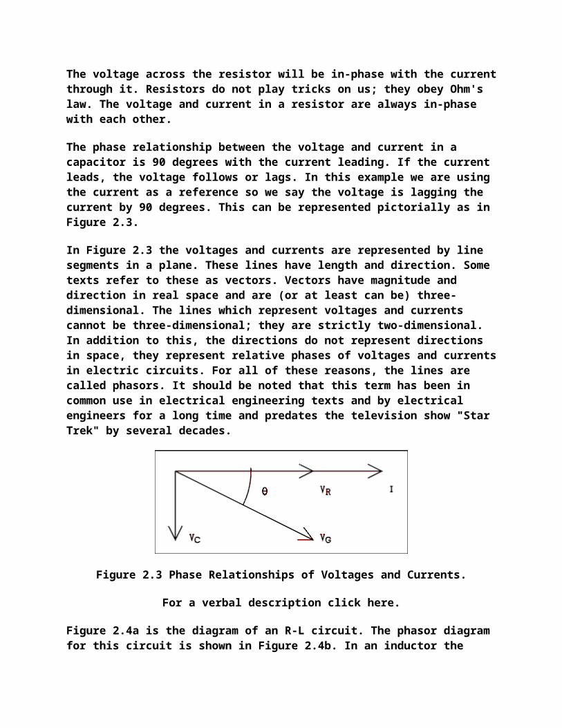
A square wave which has voltage levels of +V volt for the first half-cycle and -V volt for the second half-cycle and frequency w/(2 pi ) will have the Fourier series
The Fourier series for a triangular wave which has a positive peak voltage of +V volts and a negative peak voltage of -V volts is
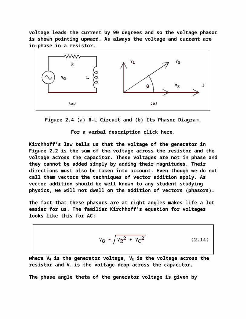
When the writer was a student, a waveform had to be capable of being described mathematically in order to obtain its Fourier series. Calculating the coefficients was a long and arduous process. Now there are computer programs which will give the coefficients of the Fourier series of any arbitrarily-shaped wave.
The Physics of It All.
Figure 2.15 Frequency Spectrum of a Square wave.
For a verbal description click here.
Figure 2.15 shows the spectrum of a square wave. Unlike spectra you are accustomed to seeing, this one plots frequency instead of wavelength. Also unlike other spectra you may have seen, the magnitude of each line is plotted upward from the horizontal axis. In optical spectra, the magnitude of each line is indicated by its brightness in a spectroscope or its darkness on a film negative. Other than that it's a perfectly normal spectrum.
Figure 2.16 shows how the sine waves fit together to make up a square wave. Notice that the square wave gets better as more harmonics are added. To obtain a perfect square wave it would be necessary to have an infinite number of harmonics. A quite good square wave is generated if approximately 99 harmonics are present.
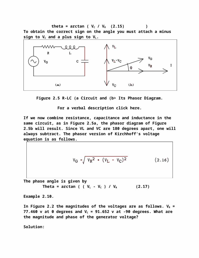
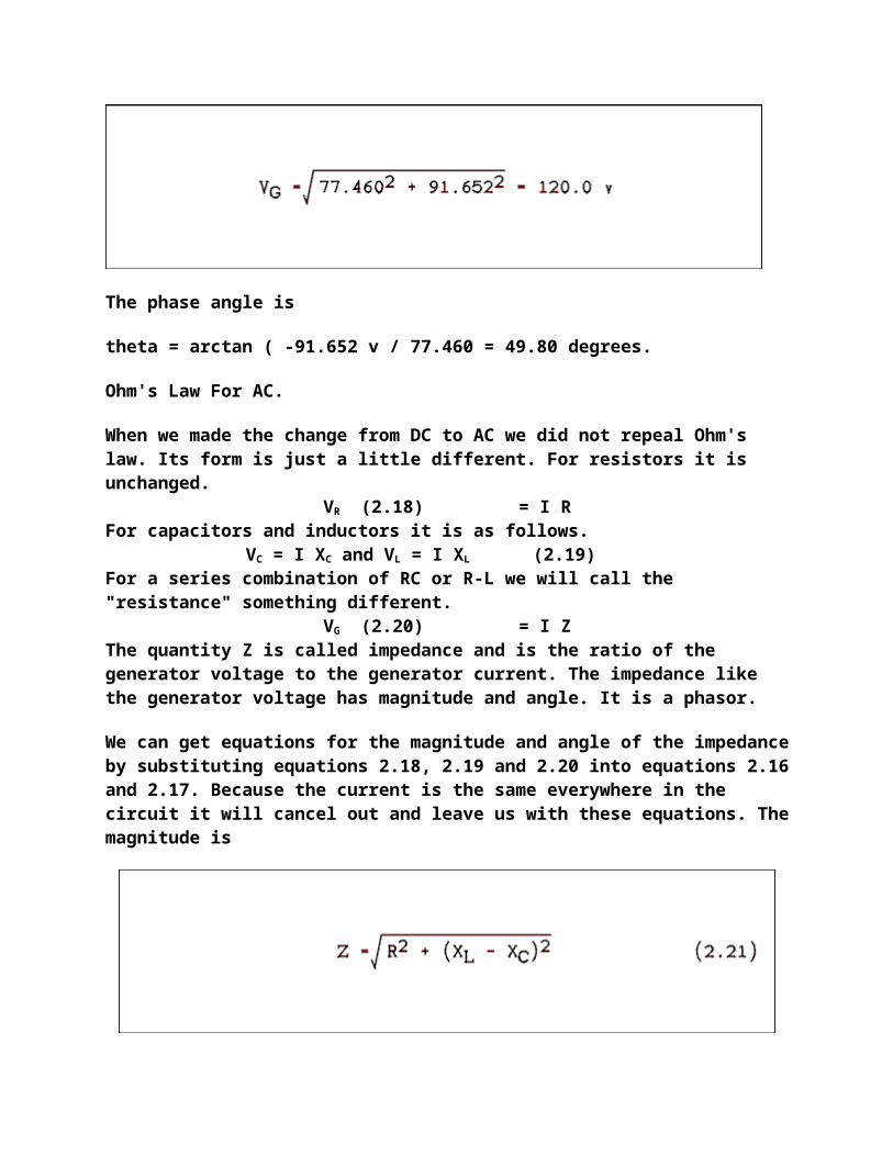
Figure 2.16 Square Waves Are Built Up from Sine Waves.
For a verbal description click here.
In the top wave the red line is the sum of the first and third harmonics. In the middle diagram the sum of 1 and 3 has been redrawn in black and the 5th harmonic added. Similarly, in the bottom diagram the 7th harmonic has been added. The more harmonics are added, the flatter the sum will be and the steeper the rises and falls will be.
2.9 The Effects of RC Circuits on Nonsinusoidal Waves.
When a nonsinusoidal wave is passed through an RC filter the shape of the wave is changed. An RC circuit cannot affect the shape of a lone sine wave. It can only affect its amplitude.
There are two different ways to look at the way in which an RC circuit changes the shape of a nonsinusoidal wave. One is to look at the way an RC circuit affects the amplitudes and phases of the harmonics (frequency domain) and the other is to look at the RC circuit as having a time constant which superimposes its own charging and discharging on the original wave (time domain).
The Frequency Domain.
Because an RC circuit affects the amplitudes of the various harmonics of a complex waveform by different amounts, the makeup of the Fourier series is changed. If you change the Fourier series, you change the shape of the wave.
Figure 2.17 shows how a square wave is modified by being passed through a low-pass RC filter. In Figure 2.17a the cutoff frequency of the filter is 10 times the frequency of the square wave. Harmonics 1, 3, 5, 7 and 9 are passed with little or no attenuation. Harmonics numbers 11 and higher are not removed; they are reduced in amplitude compared to what they were in the original wave. In Figure 2.17b the frequency of the square wave is equal to the cutoff frequency of the filter. All of the harmonics are altered in amplitude. As you can see the wave no longer looks much like a square wave. It should be pointed out that the wave has been turned on for some time, we only started looking at it where the wave seems to start. Starting and stopping transience are not shown.
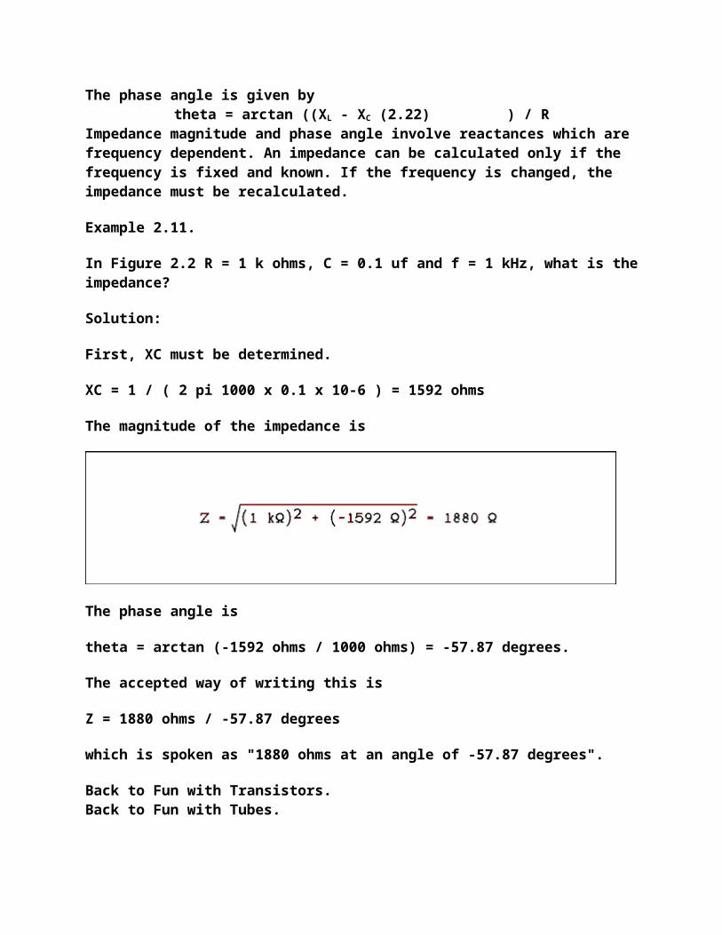
Figure 2.17 RC Filter's Effects on a Square wave.
For a verbal description click here.
In Figure 2.17c the vertical scale has not been changed. The square wave has been changed into a triangular wave of somewhat reduced amplitude. The filter has imposed its own 1 over f function on the harmonics of the square wave. The harmonic amplitudes of the wave are now a 1 over f squared function. Look at the Fourier series for a triangular wave and you will see that it is a 1 over f squared function. The square wave has been converted into a triangular wave.
The analysis of other waveforms is not as easy as for a square wave but the principle is the same. In general a low- pass filter will tend to round off the sharp edges on any wave.
Figure 2.18 shows how a square wave is modified by being passed through a high-pass RC filter. In Figure 2.18a the cutoff frequency of the filter is 10 times the frequency of the square wave. Harmonics 1, 3, 5, 7 and 9 are severely attenuated with the lower numbered harmonics being attenuated more than the higher numbered ones. Harmonics numbers 11 and higher are passed with little or no attenuation. The result is a series of spikes as shown in Figure 2.18a. As with Figure 2.17, starting and stopping transients are not shown.
Figure 2.18 RC Filter's Effects on a Square wave.
For a verbal description click here.
In Figure 2.18b the cutoff frequency of the filter is equal to the fundamental frequency of the square wave. The fundamental frequency (first harmonic) of the wave will be attenuated by 3 dB while the higher harmonics will be affected very slightly. In Figure 2.18c the frequency of the wave is 10 times the cutoff frequency of the filter. The first harmonic will be affected by only about 10%. Figures 2.18b and 2.18c show how sensitive a square wave is to the amplitude of its fundamental frequency.
The Time Domain.
In Figure 2.17 a square wave is being passed through an RC low-pass filter. When the input wave changes states, say from -V to +V, the capacitor must charge up from -V to +V. As you will remember it takes one time constant for the voltage to reach 36.8% of the final value. Theoretically, the voltage will never reach the final value.
In Figure 2.17a there are 31.4 time constants in every half cycle of the square wave. This means that the capacitor has plenty of time to charge up to the final value. The difference between the final value and the charge on the capacitor is 2.27 x 10⁻¹⁴. In Figure 2.17b there are only 3.14 time constants in each half cycle. The capacitor has much less time to finish charging before the square wave switches to its other state. Even so the voltage will have time to reach 95.7% of its final value. In Figure 2.17c there is only 0.314 of a time constant in each half cycle of the square wave. The voltage will only reach 26% of its final value. For small values of x the equation y = e-x appears to be a straight line. That is why the square wave is converted into a triangular wave.
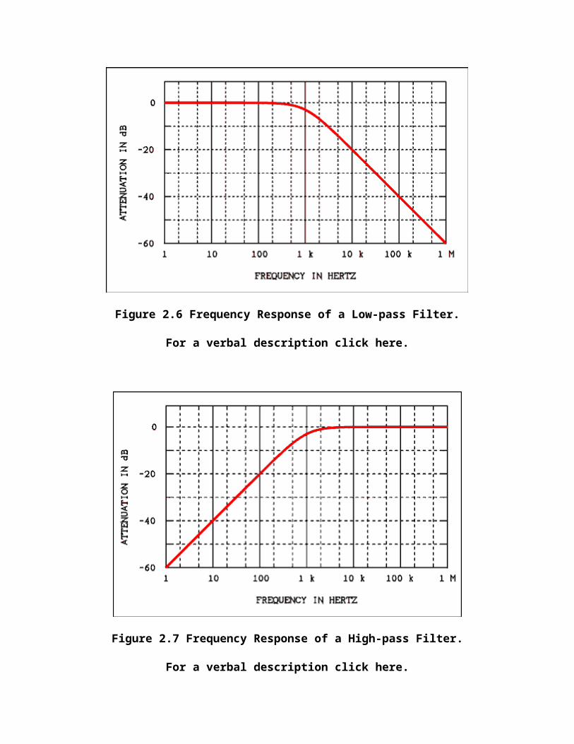
The time integral of a square wave is a triangular wave. RC low-pass filters are often called integrators because they can be made to integrate waves if the frequency of the wave is higher than the cutoff frequency of the filter.
If a square wave is passed through an RC high-pass filter the results are shown in Figure 2.18. In Figure 2.18a there are 31.4 time constants in every half cycle of the square wave. This means that the capacitor has plenty of time to discharge. The charge on the capacitor is 2.27 x 10⁻¹⁴ of its starting value. In Figure 2.18b there are only 3.14 time constants in each half cycle. The capacitor has much less time to finish discharging before the square wave switches to its other state. Even so the voltage will have time to reach 4.3% of its initial value. In Figure 2.18c there is only 0.314 of a time constant in each half cycle of the square wave. The voltage will fall to 73% of its initial value.
RC high-pass filters are often called differentiating circuits because they do an approximate differentiation on the input wave. The slope of a square wave is 0 along the flat portions of the wave and very high on the transitions. Thus the derivative of a square wave is a series of narrow spikes similar to Figure 2.18a.
The fact that the same set of figures was used for both time domain and frequency domain discussions should make it clear that these are simply two different ways of describing the same phenomenon. The physics goes on regardless of the human reasoning process or even in the total absence of human reasoning.
2.10 R-LC Resonate Circuits.
When inductance and capacitance exist together in the same circuit the phenomenon of resonance appears. You are already familiar with resonance in a spring-mass system. If such a mechanical system is driven by an external force at different frequencies it will respond most strongly when driven at its resonant frequency. If the system is displaced and then released, it will produce damped oscillations at its resonant frequency. How rapidly the oscillations damp out will depend on the amount of energy lost in the system.
An R-LC circuit will respond electrically in exactly the same way as the mechanical system. If an external AC voltage is applied to the circuit at different frequencies, the current in the circuit will be largest at the resonant frequency. If a DC voltage is applied to the circuit and then suddenly removed, the circuit will produce damped oscillations at its resonant frequency. How rapidly the oscillations damp out will depend on the amount of resistance in the circuit.
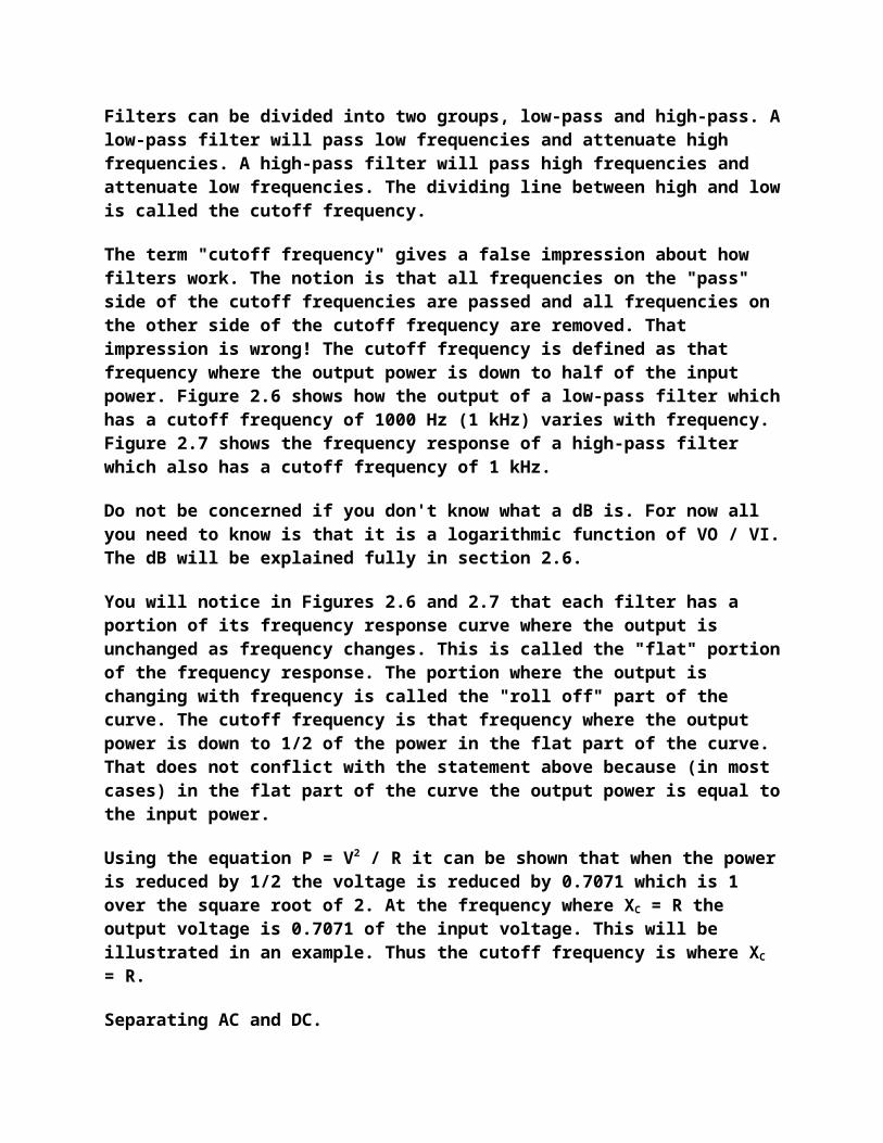
Figure 2.19 (a) R-LC Resonant Circuit and (b) Phasor Diagram.
For a verbal description click here.
A series R-LC circuit is shown in Figure 2.19a and its phasor diagram is shown in Figure 2.19b. The current everywhere in the circuit will be in phase with itself. The voltage across the resistor will be in phase with the current. The voltage across the inductor will lead the current by 90 degrees while the voltage across the capacitor will lag the current by 90 degrees. As can be seen in Figure 2.19b the total difference in phase between VC and VL is 180 degrees. IF the two voltages are equal in magnitude, they will cancel out and the voltage across the resistor will be equal to the generator voltage. Whereas IC = IL, the only way to make VC = VL is to have XC = XL. This is the definition of the resonant condition in a series circuit. Series resonance occurs when the capacitive reactance is equal to the inductive reactance.
The total impedance of a series R-LC circuit is
where R is the resistance of the resistor in ohms, XL is the reactance of the inductor in ohms and XC is the reactance of the capacitor in ohms. If we substitute XL = 2 pi fL and XC = 1/(2 pi fC) we have
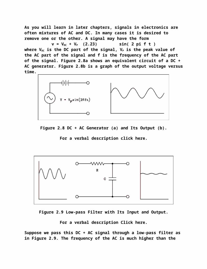
where f is the frequency in hertz, L is the inductance in henrys and C is the capacitance in farads. With R, L and C held constant Z will be infinite at f = 0 and infinity. For values of f between zero and infinity, Z will come down to a minimum of Z = R at the resonate frequency. Figure 2.20 shows impedance versus frequency and current versus frequency for a 1 volt generator, a 50 ohm resistor, a 79.6 millihenry inductor and a 0.318 microfarad capacitor connected as in figure 2.19a. The curves of resonant circuits appear on linear scales about as often as they appear on log scales.
Figure 2.20 Impedance and Current Versus Frequency.
For a verbal description click here.
Resonant circuits are used to select a narrow band of frequencies out of the entire frequency spectrum. Just how narrow a band is selected depends on the quality factor "Q" of the circuit.
Bandwidth and Q of Resonant Circuits.
The bandwidth of a resonant circuit is defined as the difference between the two frequencies where the current is down to 0.707 of its maximum value (the half power points). Remember that 0.707 is our old friend -3 dB. This is a somewhat arbitrary definition as in the case of RC filters. In the circuit of Figure 2.20 the maximum circuit
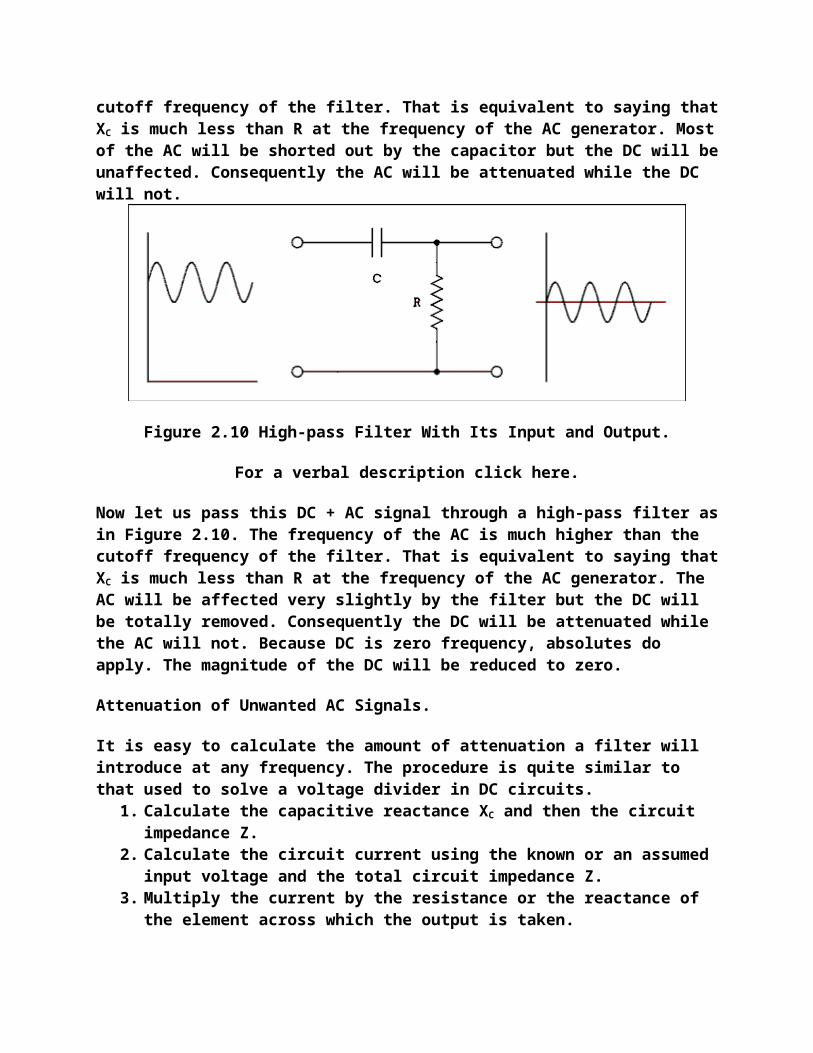
current is 20 mA. The current at the -3 dB point is 14.14 mA. Notice that there are two -3 dB points on the curve at frequencies of 952 and 1052 hertz. *
The lower -3 dB frequency is called f1, the upper -3 dB frequency is called f2 and the resonant frequency is called fR. The quality of a resonant circuit may be expressed as
* These frequencies were found by placing a conditional test in the plot program and causing the frequencies to be printed out. In this sense the values were "picked off of" the graph.
Q = fR / (f2 - f1 (2.38) ) The Q or quality factor of a resonant circuit can also be expressed as follows:
Q = XL Q = X or / R c (2.39) / R Q is defined at resonance where XL = XC. Equations 2.38 and 2.39 are based on definitions and so cannot be derived. An equation which would arise from setting equations 2.38 and 2.39 equal is an approximation which falls apart if Q is less than about 5.
Example 2.19.
What is the resonant frequency of the circuit whose curves are plotted in Figure 2.20? Calculate the Q according to both definitions.
Solution:
The resonate frequency is where XL = XC. Equating these two quantities gives
2 pi f L = 1 / (2 Pi f C)
Solving this equation for f gives
Substituting L = 79.6 mH and C = 0.318 uf gives the result 1000 hertz. The Q of the circuit according to equation 2.38 is Q = 1000 / (1052 - 952) = 10. The values of f1 and f2 were given on page 108. To find the Q by equation 2.39 we must first find a value for XL or XC at the resonant frequency. XL = 2 pi f L = 500 ohms. Q = X/R = 500 ohms /(50 ohms ) = 10.
Example 2.20.
Using all of the same values from the previous example, what is the voltage across the capacitor in the circuit of Figure 2.19a at the resonant frequency?
Solution:
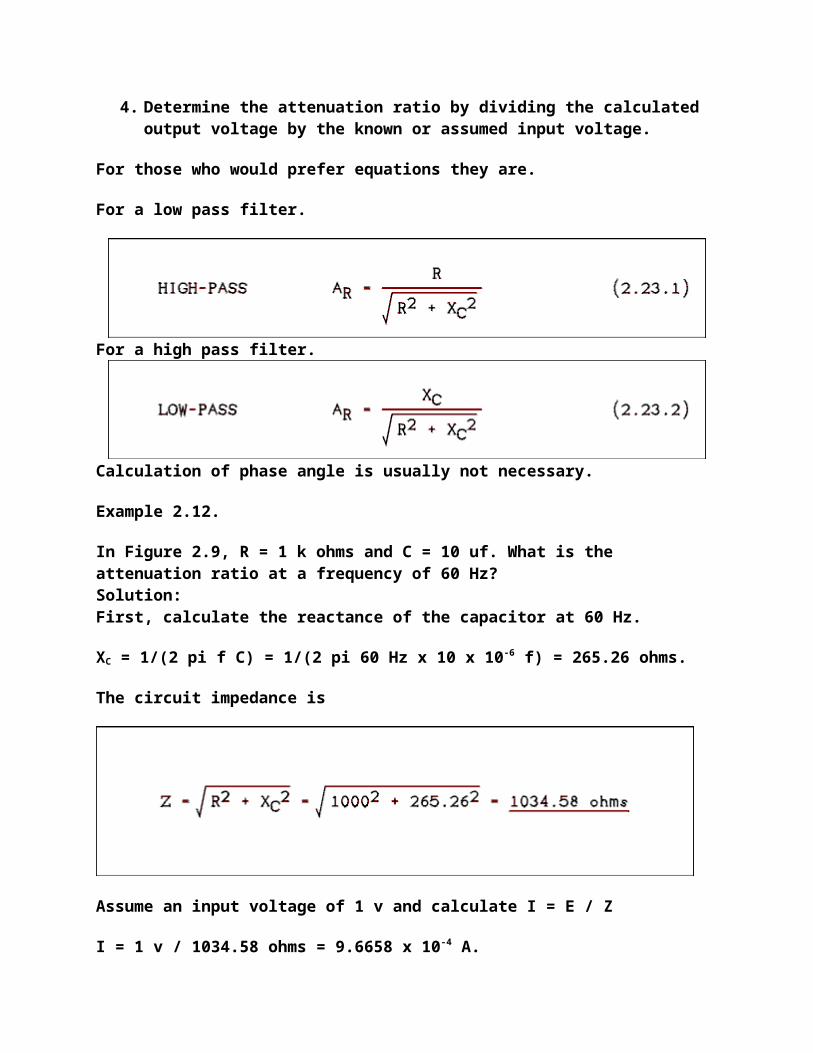
At resonance XL = XC and by equation 2.37 Z = R; therefore, I = 1 v / (50 ohms) = 20 mA. The reactance of the capacitor at resonance is XC = 1 / ( 2 pi fC ) = 500 ohms. The capacitor voltage VC = I XC = 20 mA x 500 ohms = 10 v.
Notice that the voltage across the capacitor is Q times the input voltage. This is no coincidence. The voltage across the capacitor could be taken as the output voltage of the circuit. In that case only the voltages at or near resonance will be increased in amplitude. Voltages at frequencies far away from resonance will be attenuated.
One note of caution. The circuit is NOT increasing the power of the input signal. While more voltage is available, there is less current available. You don't get something for nothing.
Also you have no doubt noticed that f1 and f2 are not equally spaced about fR. Reactive circuits behave in a geometrical rather than an arithmetical manner. That is to say f2 - fR is not equal to fR - f1 but
f2 / fR = fR / f1 in this example to an accuracy of 0.15%. (The accuracy might have been better but the frequency was restricted to integer values.) The curve would be graphically symmetrical if it had been plotted on a logarithmic frequency scale. The Q of a circuit which resonates at a radio frequency can be as high as 250. The curves of such circuits cover such a small percentage of the frequency spectrum that there is no practical difference between a logarithmic and a linear scale.
The Imperfect Inductor.
In the study of electric circuits we are accustomed to thinking of every component as if it were perfect. We think of wires as having zero resistance, resistors as having exactly the specified value and capacitors as having no built-in resistance. The errors which result from these implicit assumptions are not large enough to get us into very much trouble. Of the three basic circuit components - resistors, capacitors and inductors - inductors are the most imperfect. To assume that inductors possess only the property of inductance would be a very large mistake.
Inductors are constructed by winding a length of copper wire on a hollow nonmagnetic, nonconducting tube (air core) or an iron bar (iron core). Other core materials are used such as powdered iron (ferrite) or brass. Both the wire and the core material introduce energy losses. When energy is lost, the effect is the same as having resistance in series with the inductor.
The copper wire actually has resistance. Certain inductors have many turns which means that the total length of wire is quite long. The amount of resistance can be significant enough to lower the Q of the circuit.
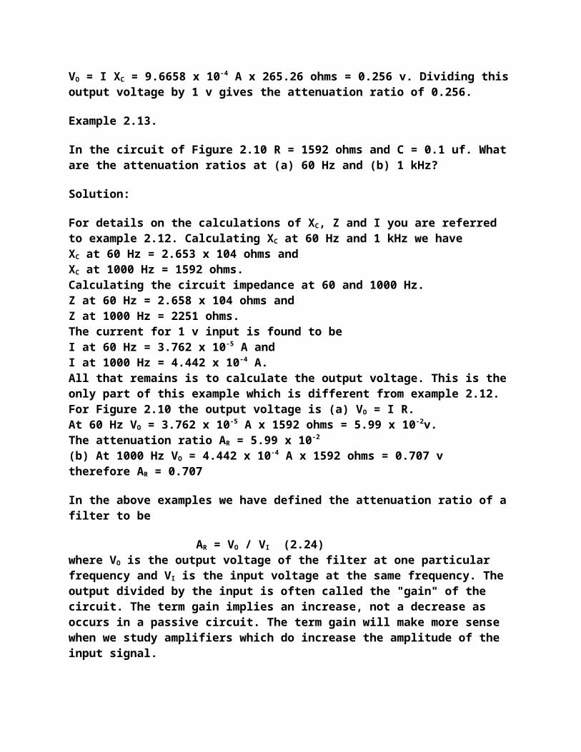
Figure 2.21 Equivalent Circuit of an Inductor.
For a verbal description click here.
The loss which is introduced by the core material also contributes to the equivalent resistance of the inductor. Any energy loss in a circuit can be accounted for by calling it resistance even though there is no measurable resistance in the circuit. A core which has losses will cause the inductor to act the same as if a lossless inductor were connected in series with a real resistor.
You may be wondering why iron and material other than air are used. If the only thing a core did was to introduce losses there would be no reason to use it. An iron core will increase the amount of inductors by as much as a factor of 1000 over the same coil with an air core. The gain in inductance is well worth the increase in core loss caused by the iron.
If iron is so good, why use anything else? The reason is frequency. The common laminated iron core* is only useful through the audio frequency band (up to 20,000 Hz). Powdered iron cores are useful up to about 30 MHz. The individual grains of iron powder are held together and insulated from one another by some sort of plastic material. Brass cores are used from about 30 to 200 MHz. Above 200 MHz even air core coils have only 2 or 3 turns and a solid core is not needed to increase the inductance.
* A solid iron core is useless in AC applications because of the excessive losses due to eddy currents. In a laminated core the iron is in thin sheets and the sheets are electrically insulated from one another.
Parallel Resonant Circuits.
Figure 2.22 is the diagram of a parallel resonant circuit. Circuits such as this are used much more often than are series resonant circuits. The impedance versus frequency curve for this circuit is shown in Figure 2.23. As you can see, the impedance is low at the extremes of frequency and rises to a maximum value at resonance. If a parallel resonant circuit is used as the load for a transistor, the gain of the amplifier will be maximum at resonance and very low away from resonance. Such an amplifier is called a frequency-selective or tuned amplifier.
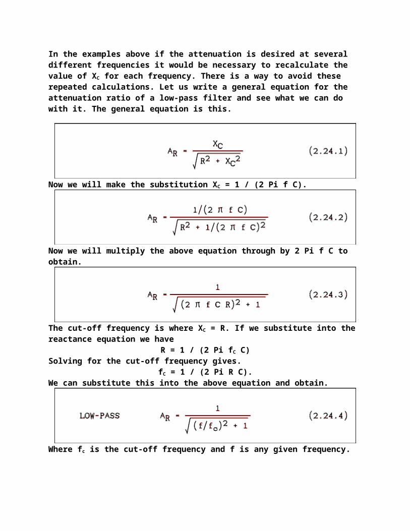
Figure 2.22 Parallel Resonant Circuit.
For a verbal description click here.
Figure 2.23 Impedance Versus Frequency for a Parallel Resonant Circuit.
For a verbal description click here.
2.11 Transformers.
A transformer is a device which will change the voltage and current of AC. A transformer can be used to step down the voltage of the power line for use by circuits which would be damaged by the full 120 volts of the power line. In addition the electric utility itself uses
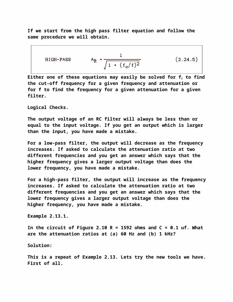
transformers to step the voltage up and thereby step the current down to minimize the power lost in long power lines. A transformer consists of two or more coils of wire wound on an iron core. The coils are usually wound one surrounding the other. The schematic symbol for a transformer is shown in Figure 2.24. The winding to which power is applied is called the primary winding and the winding from which the power is taken is called the secondary winding. Many transformers have more than one secondary winding.
Figure 2.24 Symbol for a Transformer.
For a verbal description click here.
To determine quantitatively how the voltage is changed by a transformer we must remember the equation
where E is the voltage across the coil, N is the number of turns on the coil and Phi is the magnetic flux linking the coil. For the two windings of a transformer we can write
where the subscript P refers to the primary and the subscript S refers to the secondary. In a transformer the magnetic flux is so well confined by the iron core that almost all of the flux from the primary also links the secondary and visa versa. This means that Phi sub P = Phi sub S. We can divide equation 2.42a through by NP and equation 2.42b by NS and set them equal and rearrange terms to obtain the following equation.
EP / ES = NP / NS (2.43)
Example 2.21.
A transformer has 2450 turns on its primary and 700 turns on its secondary. If 120 volts is applied to the primary, what is the secondary voltage?
Solution:
The secondary voltage is ES = EP NS / NP = 120 x 700 / 2450 = 34.29 volts.
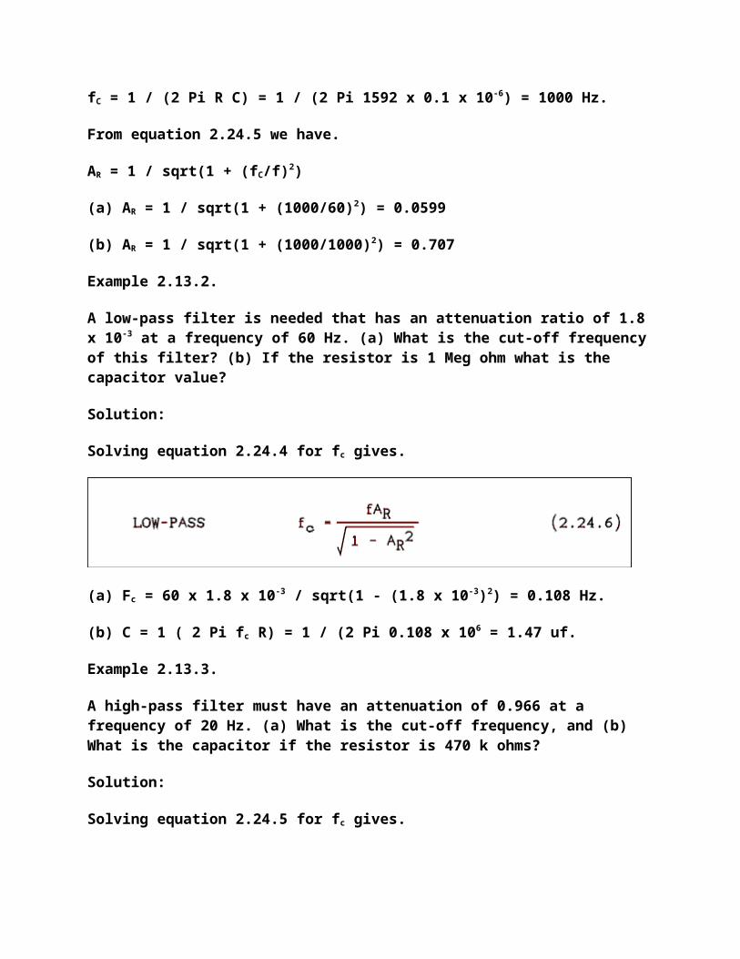
Example 2.22.
In the case of the transformer from example 2.21 if the secondary current is 850 mA, what is the primary current?
Solution:
Transformers are so efficient that the efficiency may be taken as 100% without introducing serious errors. Therefore, the power in the secondary equals the power in the primary. PP = PS and EP IP = ES IS; therefore,
IP / IS = ES / EP (2.44)
and so IP = 850 mA x ( 34.29 v / 120 v ) = 243 mA.
From equation 2.44 you might properly deduce that
IP / IS = NS / NP (2.45)
A transformer which steps up the voltage will step down the current and vise versa. An electric utility will use transformers to step up the voltage to a very high value (as much as 300 kv) to send power over very long distances. When the voltage is stepped up, the current is stepped down. Most of the loss in power transmission lines is due to the resistances of the wires. Making the current as small as possible will minimize the power loss due to resistance. The voltage is stepped back down for distribution around cities and stepped down again just before being delivered to the customer.
Impedance Transformation.
A note about terminology
The term "impedance" is often used when the term resistance could be applied. This is correct usage because of the way in which impedance is defined. Impedance is a combination of resistance and reactance. The reactive component may or may not be zero. Therefore, it is possible to say "impedance" and mean "resistance". The reverse of this is not correct.
The apparent impedance of the primary of a transformer is given by ZP = EP / IP and the impedance in the secondary is ZS = ES / IS. If we substitute equations 2.43 and 2.45 into these impedance equations we have
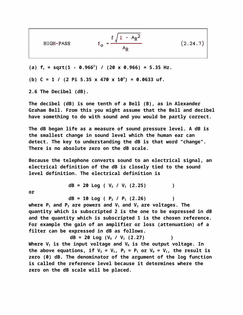
Inverting the denominator and multiplying we have.
Example 2.23
What is the turns ratio of a transformer to match an 8 ohm speaker to a 600 ohm line?
Solution:
Since power goes to a speaker, the 8 ohm speaker side is the secondary of the transformer. The power flows from the transformer to the speaker.
True, the number of turns must be an integer. A transformer manufacture would use many turns possibly 866 / 100 or more likely 8660 / 1000. Since we are working problems and not manufacturing transformers we can be content with what ever number comes out, even a number less than one.
2.12 The Oscilloscope.
Almost all voltmeters have ranges designed for measuring AC voltage. Most DMMs have ranges for measuring AC current. If sine waves are involved, most voltmeters and ammeters will read out only the RMS value of the voltage or current. The limitations of voltmeters and ammeters are many. They cannot tell us anything about the waveform, the frequency, the phase or noise content of the AC signal being measured. Indeed, if the waveform is other than a sine, if the frequency is too high or if the signal contains too much noise, common AC voltmeters and ammeters will give us false readings.
The most useful instrument for making measurements on AC signals is the oscilloscope. The oscilloscope can be used to make quantitative measurements of voltage, frequency, rise-time of a square wave and phase between two signals. In addition an oscilloscope can be used to make qualitative evaluations of waveform and noise content. But that's not all. With various electronic and computer add-ons an oscilloscope can display the characteristic curves of semiconductor devices, plots of frequency response, phase diagrams of complex signals and frequency spectra and logic states (1s and 0s) in a
microprocessor system. If you had to do electronics in a remote area of the earth or in space and you could take only one measurement instrument, the oscilloscope would be the unquestioned choice.
An oscilloscope is basically two instruments in one: a voltmeter and a time interval meter. The voltmeter portion is usually the Y axis, although the X axis may be used in some oscilloscopes for some special applications. The time interval portion is always the X axis.
The thing which sets the oscilloscope apart from all other electrical measurement instruments is the cathode ray tube (CRT). The CRT is one of the few vacuum devices which has not been replaced by a solid state equivalent. (For some years now the solid state replacement has been promised but so far it remains only a promise.)
BINGO! That promise has at last been fulfilled. I have, at this moment, sitting on my workbench an oscilloscope which has a front panel the same size as any classic scope but instead of being seventeen and a half inches deep it is four and a half inches deep. The CRT has been replaced by a liquid crystal display. Granted, at this writing, 2006, they are still rather pricy. But knowing the electronics industry, the price will come down and the CRT will fall out of favor, except for a small number of diehards who will insist that the CRT just looks better. I have to concede that is true but the advantages still outweigh the disadvantages. The following section on the CRT will be left in until this tube completely disappears from the scene.
The Cathode Ray Tube.
A simplified, two-dimensional drawing of a CRT is shown in Figure 2.25. Electrons are emitted from the heated cathode and are formed into a fine beam and raised to a high velocity by the accelerating electrode assembly. When the electron beam strikes the screen, a small dot of light appears. The color of this light depends on the material used in the screen.
Between the electron "gun" and the screen are two pairs of deflection plates. One pair is for deflecting the electron beam in the horizontal plane and the other set deflects the beam in the vertical plane.
Figure 2.25 Simplified, Two-dimensional Drawing of a CRT.
For a verbal description click here.
If the potential difference between the deflection plates is zero, the beam will fall in the center of the screen. Suppose that we make the top Y deflection plate positive with respect to the bottom one. Since like charges repel and unlike charges attract, the electron beam will be bent upward on its way to the screen and will strike the screen above the center. If the potential is reversed, the beam will be bent downward. The X deflection plates work in the same way to bend the beam in the horizontal plane. The voltage between the deflection plates is quite large, usually about 50 volts to move the dot one inch.
A block diagram of an oscilloscope is shown in Figure 2.26. We will briefly discuss each block. Because we have not yet studied amplifiers, we cannot look at specific circuits in this chapter.
The Vertical Amplifier.
Because of the high voltage required to deflect the electron beam, it is necessary to include an amplifier in an oscilloscope. As shown in the block diagram of Figure 2.26, the amplifier is between the Y input and the Y deflection plates of the CRT. The amplifier includes range switches to permit measurement of voltages from very small (1 millivolt) to somewhat large (100 volts). There is also a control to allow the operator to position the display anywhere on the screen (or even off of it). Some oscilloscopes have switches for reversing the polarity of the signal (turning the display upside down).
The vertical input is not only to look at the pretty picture. It can be used to measure voltage. There is a range switch which is calibrated in volts per division on the screen. This allows the oscilloscope to be used as a voltmeter to measure unknown voltages.
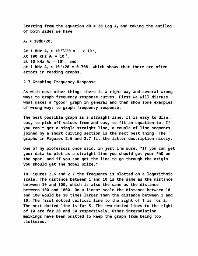
The Time Base.
In order to plot voltage versus time (which is what an oscilloscope does best), it is necessary to move the dot of light across the screen at a constant velocity. This is done by placing a ramp voltage on the horizontal deflection plates. A ramp voltage is one which is increasing at a constant rate and would have the equation V = Kt where K is a constant. Plotted versus time, such a voltage will be a straight upward-sloping line. The time base is often called the "sweep" because the electron beam is swept across the screen. The sweep is calibrated in time per division on the scope screen and a switch selects the various sweep rates.
The dot of light begins at the left edge of the screen and is swept across to the right edge. Before the sweep is returned to its starting point, the electron beam is turned off to darken the dot so that the return sweep will not be visible and confuse the operator. The beam retraces to the left hand edge of the screen in a small fraction of the time required to sweep from left to right. Upon reaching the left edge of the screen, the electron beam is turned on again and the dot begins another trip across the screen.
Figure 2.26 Block Diagram of an Oscilloscope.
For a verbal description click here.
Triggered Sweep.
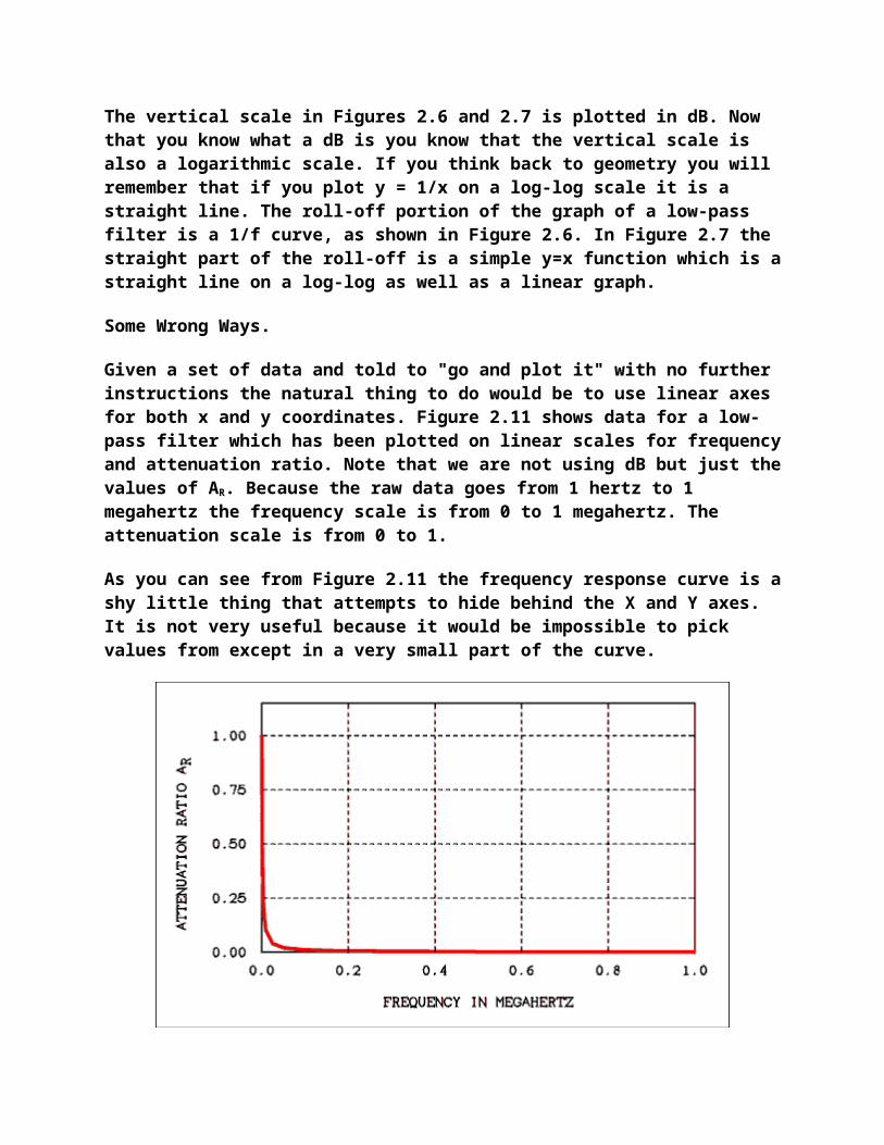
The beam does not begin another trip across the screen immediately; it waits until some triggering event has occurred. The beam is kept dark until it is triggered. When triggered, it is turned on and begins another trip across the screen. The wave on the Y axis is, in most cases, what triggers the sweep to begin.
Because the sweep begins at the same point on the wave every time it repeats, successive sweeps fall exactly on top of each other and what the user sees is a stable display.
The Power Supply.
The power supply provides high voltage to the CRT to accelerate the electrons to a high enough velocity to make the screen glow. It also supplies operating voltages to all of the circuits in the oscilloscope. There are no operator adjustments in the power supply (unless you count the ON OFF switch).
Reading the Oscilloscope.
There are lines etched on the inside of the CRT screen which divide the screen into squares which are one centimeter on a side. The squares are further divided into 0.2 cm by small hash-marks. For some reason, oscilloscope manufacturers no longer call a cm a cm. They now call it a div for division.
The range switch of the voltmeter section is usually called the "volts/div" switch. To read the voltage being measured by an oscilloscope it is necessary to read the height of the wave on the screen (in div) and multiply it by the setting of the range switch.
Example 2.24.
A wave on the screen of an oscilloscope has a vertical distance between its positive and negative peaks of 5.35 div. The range switch is set to 0.2 volts/div. What is the peak-to-peak voltage of the wave?
Solution:
The peak-to-peak voltage usually written as the P-P voltage is the product of the peak-to-peak distance and the range switch setting. The P-P voltage is 5.35 div x 0.2 v/div = 1.07 volts.
The horizontal axis of an oscilloscope is actually a time interval meter. The range switch for the time interval meter is the time/div or sec/div (seconds per division) control. To make a time interval measurement it is necessary to multiply the horizontal distance between the two points by the setting of the sec/div switch.
Example 2.25.
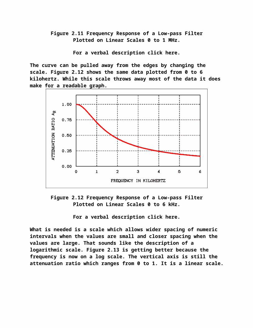
The width of a pulse on the screen of an oscilloscope is 7.3 div and the sec/div switch is set to 5 us/div. What is the width of the pulse in units of time?
Solution:
The pulse-width is 7.3 div x 5 us/div = 36.5 us.
Example 2.26.
Eight cycles of a sine wave cover 4.45 divisions on the screen of an oscilloscope and the sweep range is set to 0.5 us/div. What is the frequency of the sine wave?
Solution:
The sweep range is just another name for the sec/div switch. The frequency is in hertz, which is cycles/sec.
f = 8 cycles / (4.45 div x 0.5 us/div) = 3.60 MHz.
The Times Ten Probe.
The input impedance of an oscilloscope is rather low as voltmeters go. A typical value is 1 M ohms of resistance in parallel with 50 pf of capacitance. For most measurements the resistance needs to be higher and the capacitance lower than the input impedance as stated.
Higher resistance and lower capacitance can be obtained by using a special probe with the scope. The input end of the probe contains a 9 M ohms resistor in parallel with a 50/9 pf capacitor. The 9 M ohms resistor in conjunction with the 1 M ohms resistance of the scope input will give a total input resistance of 10 M ohms but it will attenuate DC and low frequency input signals by a factor of ten. The capacitor in the probe must have an XC which is 9 times that of the XC of the input capacitance of the scope so that high frequencies are also attenuated by a factor of ten. The capacitor in the probe is adjustable and the probe should be "calibrated" before it is used.
2.13 Problems.
1. What is the period of an AC signal which has a frequency of 2175 hertz? 2. An oscilloscope measurement shows a wave to have a period of 2.2 us. What is its
frequency? 3. What is the wavelength in meters of a radio wave whose frequency is 162.25 MHz? 4. What is the frequency of a 75 meter long radio wave? 5. What is the angular frequency of the 60 hertz line? 6. What are (a) the peak and (b) the peak-to-peak voltages of the 120 volt AC line? 7. An oscilloscope measurement shows an AC sine wave to have a peak-to-peak value
of 9.5 volts. What is its RMS voltage? 8. What is the reactance of a 470 uf capacitor at a frequency of 120 hertz?
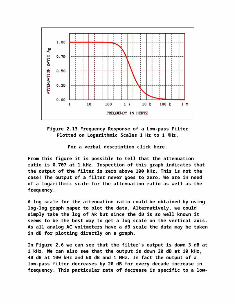
9. What size capacitor is required to have a reactance of 1 ohm at a frequency of 60 hertz?
10. If a 100 uf capacitor is connected across a 10 volt 400 hertz AC source, how much power is dissipated by the capacitor.
11. What is the reactance of a 2.5 mH coil at a frequency of 455 kHz? 12. How much inductance is required to have a reactance of 1000 ohms at a frequency
of 1000 hertz? 13. In a series RC circuit the voltage across the resistor is 4.4 volts and the voltage
across the capacitor is 3.5 volts. The resistance of the resistor is 560 ohms and the frequency is 60 hertz. (a) What is the reactance of the capacitor? (b) What is the capacitance of the capacitor? (c) What is the magnitude of the generator voltage? (d) If the phase angle of the resistor voltage is taken as zero degrees, what is the phase angle of the capacitor voltage? (e) What is the phase angle of the circuit current? (f) What is the phase angle of the generator voltage?
14. A series RLC circuit is connected across a generator whose frequency is 100 kHz. The resistor is 100 ohms, the inductor is 5 mH and the capacitor is 390 pf. What are the magnitude and phase angle of the impedance?
15. An RC high-pass filter uses a .01 uf capacitor and a 15 k ohms resistor. What is the attenuation ratio of this filter at frequencies of (a) 10 hertz, (b) 1 kHz and (c) 100 kHz?
16. An RC low-pass filter is to use a 1 M ohms resistor. Select the capacitor for an attenuation of 50 dB at 60 hertz.
17. Convert the following attenuation ratios to dB: (a) 0.707, (b) 0.316, (c) 0.178 and (d) 0.0316.
18. Convert the following gain figures to dB: (a) 1, (b) 2, (c) 3.16 and (d) 17.78. 19. Obtain a piece of semi-log graph paper and plot the frequency response data given below.
See also problem 20 below. Frequency, Hz dB Frequency, Hz dB Frequency, Hz dB
1.00 Hz -40.0 1,000 -0.1 1,000,000 -40.0
1.78 -35.0 1,778 -0.1 --- ---
3.16 -30.0 3,162 -0.4 --- ---
5.62 -25.0 5,623 -1.2 --- ---
10.00 -20.0 10,000 -3.0 --- ---
17.78 -15.1 17,780 -6.2 --- ---
31.62 -10.4 31,620 -10.4 --- ---
56.23 -6.2 56,230 -15.1 --- ---
100.0 -3.0 100,000 -20.0 --- ---
177.8 -1.2 177,800 -25.0 --- ---
316.2 -0.4 316,200 -30.0 --- ---
562.3 -0.1 562,300 -35.0 --- ---
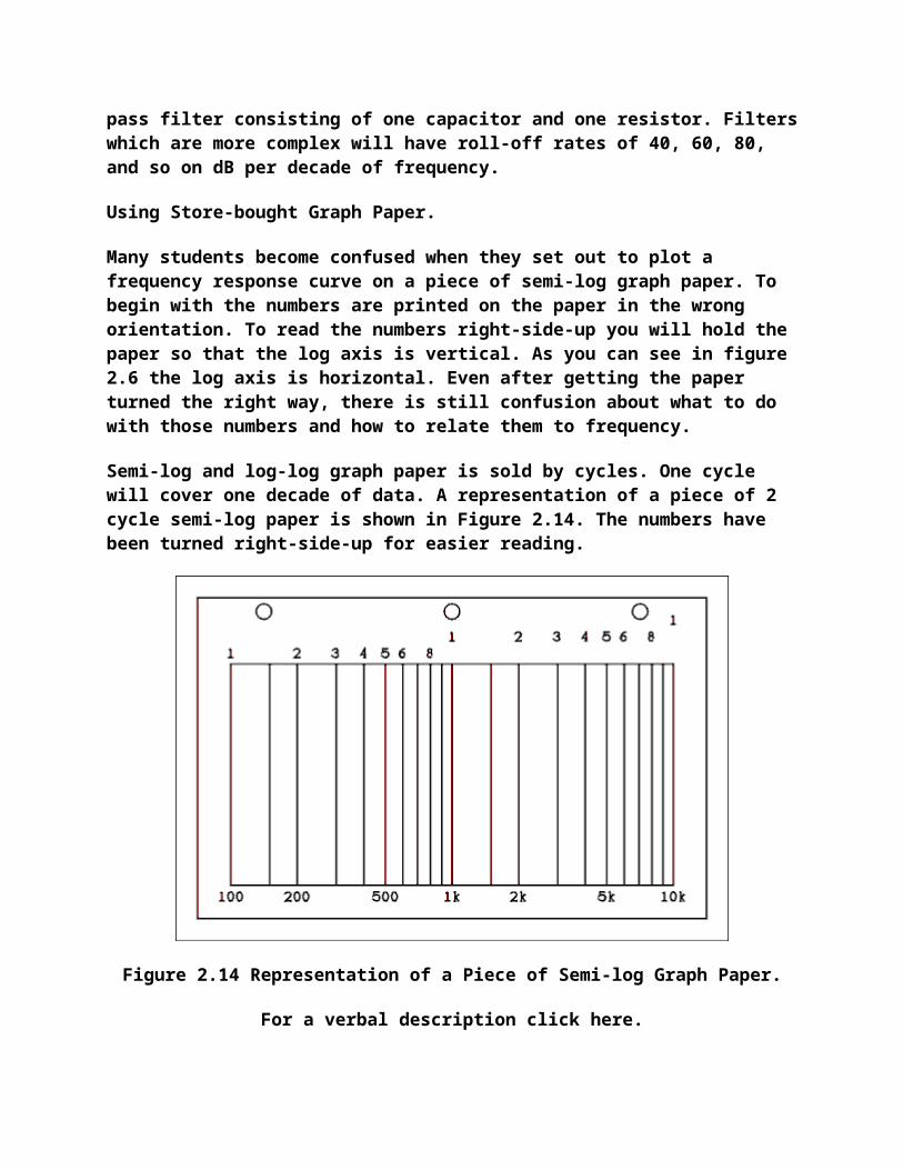
20. As an alternative to problem 19, if you cannot find a piece of 6 cycle semi-log graph paper, try this. Take the common log of each frequency. Plot dB versus log of frequency on linear paper. BUT LABEL THE HORIZONTAL AXIS OF THE GRAPH WITH FREQUENCY NOT LOG OF FREQUENCY!
21. As a more modern alternative, enter the above data into a program that will draw a graph on the computer screen or printout. Be sure to select log for the horizontal axis.
22. A square wave has a peak voltage V of 25 volts. What are the peak values of: (a) the fundamental frequency; (b) the 9th harmonic; (c) the 50th harmonic; and (d) the 99th harmonic?
23. A square wave has a peak-to-peak voltage of 266.6 volts and a frequency of 60 hertz. What is the RMS voltage of: (a) the fundamental frequency and (b) the frequency and RMS amplitude of the harmonic which falls immediately below 10 kHz?
24. What circuit would you use to convert a 60 Hz square wave into a series of narrow pulses? Draw the circuit and give one of its proper names. It is not necessary to give component values.
25. If you apply an AC plus DC voltage wave of the type VDC + VAC sin( wt ) to an integrating network which has a time constant much longer than the period of the sine wave, what will the output mainly consist of?
26. A series resonate circuit is made up of a 2.5 mH inductor, a 48.9 pf capacitor and a 100 ohms resistor. What is: (a) the resonant frequency of this circuit? (b) the Q of the circuit? And (c) the 3 dB bandwidth of the circuit?
27. In the circuit of question 26 the bandwidth is too narrow and must be increased to 30 kHz. This can be done by adding resistance to the circuit. If a resistor is added to increase the bandwidth to 30 kHz, (a) what is the new value of Q and (b) how much resistance must be ADDED to the circuit?
28. A variable inductor which is used in the laboratory has a nominal resistance of 40 ohms at a frequency of 1 kHz. What is the Q of this inductor at this frequency for inductance settings of (a) 5 mH and (b) 50 mH?
29. An all-electric home is drawing a current of 65 amperes at a voltage of 240 volts. What is the current on the primary side of the supply transformer if the voltage is 9200 volts?
30. A certain transformer has a 120 volt primary and a 40 volt secondary which is rated at 2.5 amperes maximum. What is the minimum size fuse which should be used in the primary to protect this transformer from over-Load?
31. A triangular wave is displayed on the screen of an oscilloscope. Points are given on the screen using Cartesian coordinates with the point (0,0) at the left side of the screen and centered top to bottom. The first positive peak of the wave is at (1.2,4.3), the first negative peak is at (3.9,-4.9), the second positive peak is at (6.6,4.3) and the second negative peak is at (9.3,-4.9). (a) If the voltage range is set to 20 mv/div, what is the P-P voltage? (b) If the sweep range is set to 50 us/div, what is the frequency of the wave?
32. In question 31 if a times ten probe is being used, what are (a) the P-P voltage and (b) the frequency?
2.14 Answers to Problems.
1. 460 microseconds. 2. 455 kHz. 3. 1.14 meters. 4. 4.00 MHz. 5. 377 radians per second. 6. (a) 169.7 v, (b) 339.4 v. 7. 6.72 v. 8. 2.82 ohms. 9. 2,650 microfarads. 10. Trick question. The answer is the big zero. 11. 7.15 k ohms. 12. 159 millihenrys. 13. (a) 445 ohms, (b) 5.95 microfarads, (c) 5.62 volts, (d) -90 degrees, (e) 0 degrees, (f) -
38.5 degrees. 14. 945 / -83.9 degrees. 15. (a) 9.42 x 10⁻³, (b) 0.686, (c) 1.00. 16. 0.839 microfarads. 17. (a) -3.01, (b) -10, (c) -15.0, (d) -30. 18. (a) 0, (b) 6.02, (c) 9.99, (d) 25.0. 19. Whether you use semi-log graph paper, 20. Liner graph paper, or 21. a computer program the graph you get should look like this.
For a verbal description click here.
22. (a) 31.83 v, (b) 3.537 v, (c) 0 v, (d) 0.3125 v. 23. (a) 120.0 v, (b) 0.7273 v and 9,900 Hz. 24. High-Pass Filter. Differentiating Network.
For a verbal description click here.
25. All of the DC, very little AC. 26. (a) 455.2 kHz. (b) 71.5. (c) 6.366 kHz. 27. (a) 15.18. (b) 138.3 ohms. 28. (a) 0.7854, (b) 7.854. 29. 1.696 Amps. 30. 0.8333 Amps. 31. (a) 0.184 volts. (b) 3.704 kHz. 32. (a) 1.84 volts. (b) 3.704 kHz.
This page copyright © Max Robinson. All rights reserved.
DC Power Supply Circuits. Chapter 3
Block Diagram of a Power Supply. 3.1 Protection Devices. 3.2 The 3.3 Power Transformer. The Semiconductor 3.4 Diode.3.4A The Vacuum Diode. Rectifier Circuits. 3.5 3.6 Filtering the Rectifier's Output. The Zener 3.7 Diode Voltage Regulator. Integrated Circuit 3.8 Voltage Regulators. Problems. 3.93.10 Answers to Problems.
Chapter 3.
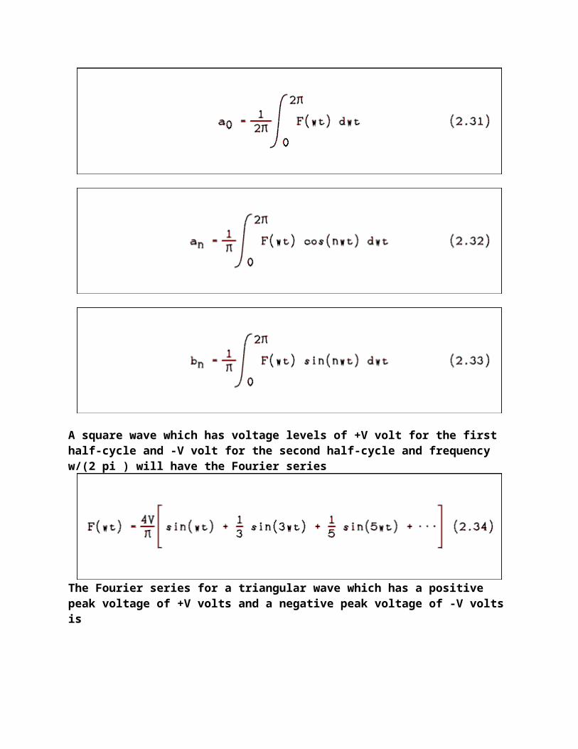
DC Power Supply Circuits.
Most of today's electronic circuits operate from comparatively low DC voltages (5 to 15 volts). The Electric Utility supplies 120 volts AC. We have studied transformers and, therefore, we know that the 120 vAC line voltage could be stepped down to the range of 5 to 15 volts but it would still be AC. The internal circuits of any device you can think of from a stereo receiver to an oscilloscope will not operate on AC. These devices must have internal circuits which change the AC to DC. Such a circuit is called a "DC power supply" or more often just "power supply".
3.1 Block Diagram of a Power Supply.
Figure 3.1 Block diagram of a power supply.
For a verbal description click here.
Figure 3.1 shows the block diagram of a modern low-voltage regulated DC power supply. Each block has a specific purpose and will be dealt with in individual sections of this chapter.
The power supply is connected to the 120 vAC power line by a plug. Many power supplies (those used in laboratory equipment) have a plug with a third wire which connects the metal chassis of the instrument to earth ground. The fuse and switch constitute the protection circuits. The fuse helps to protect the power supply against circuit component failures and mistaken connections. The switch permits the power supply to be turned on and off. The transformer steps the 120 volts of the AC line down to the value required by the devices being powered. The rectifier changes the AC from the transformer to pulsating DC. The filter reduces the magnitude of the pulsations and smoothes out the DC. The regulator reduces the pulsations to a very small value and also holds the output voltage constant regardless of the load current. The regulator also contains circuits which will shut down the power supply if the load current becomes too large or the temperature of the regulator becomes too high.
If the power supply is part of something else, such as an oscilloscope, an FM tuner, or an amplifier the output of the power supply is delivered to the internal circuits of the instrument and is not available to the operator. If the power supply is a laboratory bench power supply, its output is connected to binding posts on the supply's front panel for the purpose of powering experimental circuits. A laboratory bench power supply may also
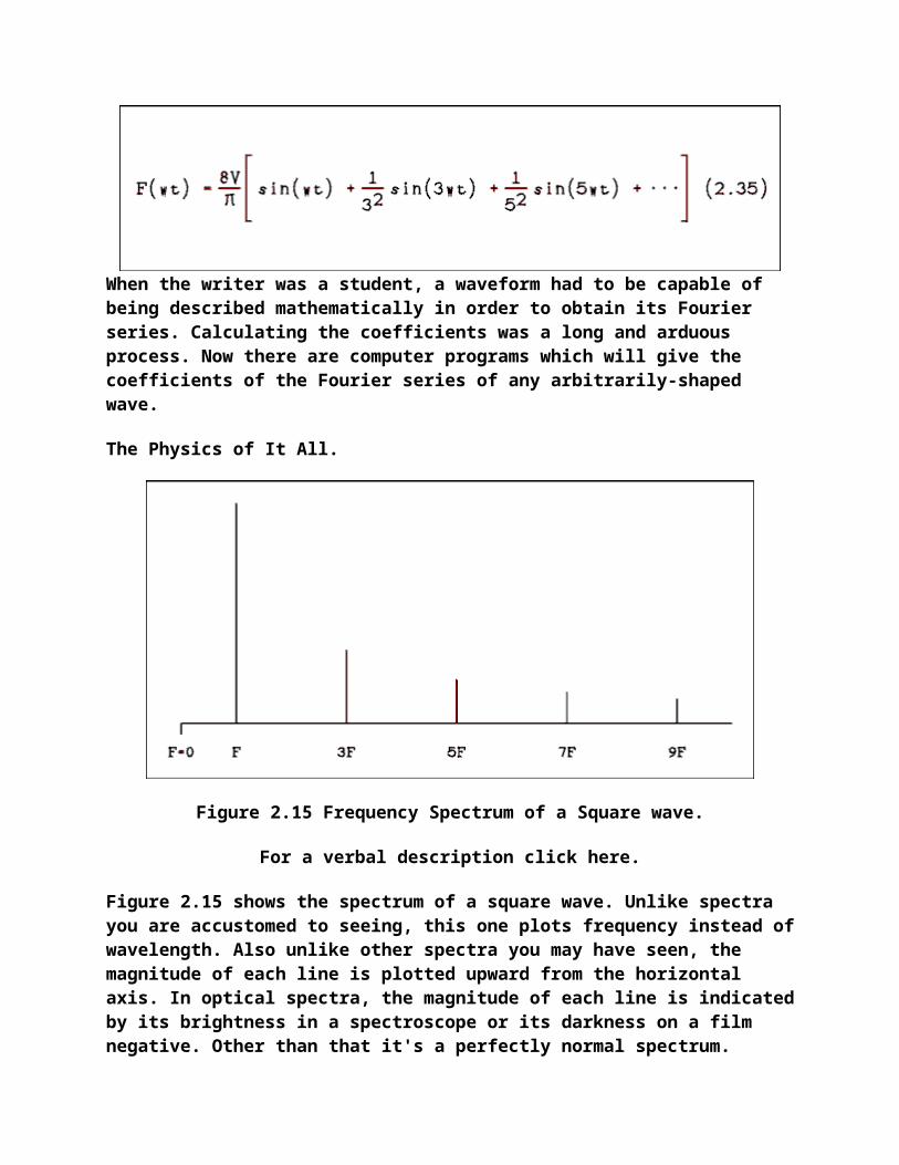
include a voltmeter and an ammeter to permit the operator to monitor the voltage and current which are supplied to the load.
3.2 Protection Devices.
All power supplies require protection from overloads and internal circuit faults. The most obvious protection device is a fuse. The type of fuse most commonly used in electronics equipment is a fine metal wire contained in a small glass tube with a metal cap on each end for electrical connection. The wire is made of a metal alloy with a low melting temperature, such as solder (40% led and 60% tin). If excessive current flows through the fuse the thin metal wire will melt, opening the circuit and turning off the current. Fuses of the type described above are manufactured in current ratings from 1/200 ampere to 30 amperes.
Fuses are often placed in the primary circuit of the transformer. If a transformer develops an internal fault it can catch fire if the power is not shut off by an open fuse. There should always be a fuse in the primary of a power transformer. Many low-cost "wall transformers" do not have fuses in their primary circuits. These units present a constant fire hazard to any building in which they are used.
There are two types of fuses, fast-acting and time delay. Time delay fuses are often called slow-blow fuses. Power supplies which have very large filter capacitors and semiconductor rectifiers will draw a very large current for a very short time after being turned on. Have you ever noticed a flicker of the lights when you turn on a transistorized stereo receiver? You are seeing the effect of a large current pulse which is charging up the capacitors in the power supply. A fast-acting fuse would most likely blow out the moment the power switch was thrown. A slow-blow fuse is used in such a case. Slow-blow fuses are used only if there is a large current pulse at the time of turn-on.
When selecting the current rating of the fuse, measure the current drawn by the device under normal operation and multiply this figure by 2. A smaller fuse than this will tend to burn out when nothing is wrong.
Other protection devices are electro-mechanical circuit breakers. A circuit breaker may use a thermal sensor to detect the heating in a small wire or the current may be detected by allowing it to flow through a coil of wire and become an electromagnet. If the temperature of the wire gets too high or the electromagnet becomes too strong, the circuit breaker will "pop out" and the circuit will be opened. The advantage of a circuit breaker is that it can be reset instead of having to be replaced, as do fuses. The major disadvantage of circuit breakers is that they are more expensive, more complex, larger and heavier than fuses. As current gets smaller, the circuit breakers get larger and more complex. Circuit breakers are usually not used for currents below 1 ampere.
In a sense the on-off switch may be considered as a protection device. If the operator smells something burning, he can use the switch to turn the power off. In a few cases a circuit breaker may serve double duty as an on-off switch. Most circuit breakers are not designed for repeated on-off cycles and will quickly wear out if used as on-off switches.

Most instruments include a small light which glows when the power is on and goes out when the power switch is turned off or the fuse blows.
3.3 The Power Transformer.
A power transformer may have a secondary winding with a center tap, as shown in Figure 3.2a, or more than one secondary winding, as shown in Figure 3.2b.
Figure 3.2 Two types of transformers.
For a verbal description click here.
For a detailed discussion of transformers refer back to Chapter 2 of this book.
If you look in a catalog listing power transformers you will not find "turns ratio" mentioned even once. The specifications of power transformers are written in terms of primary and secondary voltages and maximum secondary current. You may read the following specification, "Primary, 117 vAC 50 - 60 Hz. Secondary, 24 vCT @ 1 A." The translation of this is "The transformer will operate on 117 volts ±10% at a line frequency of 50 or 60 Hz. If you apply 117 volts to the primary the voltage across the entire secondary will be 24 volts if the secondary current is 1 ampere. The maximum current which can safely be drawn from the entire secondary is 1 ampere." If this current is exceeded the transformer is in danger of burning out due to over heating.
Example 3.1
A transformer has the following specification: "Primary, 117 vAC 60 Hz. Secondary, 32 vCT @ 1.5 A." If the primary is connected to a source of 120 vAC, what voltage is measured from one side of the secondary to its center-tap?
Solution:
The ratio of secondary to primary voltage is a constant. 32 / 117 = V / 120. V = 32.82 v. The voltage measured from one side of the secondary to the center-tap is 1/2 that of the whole secondary or 16.41 v.
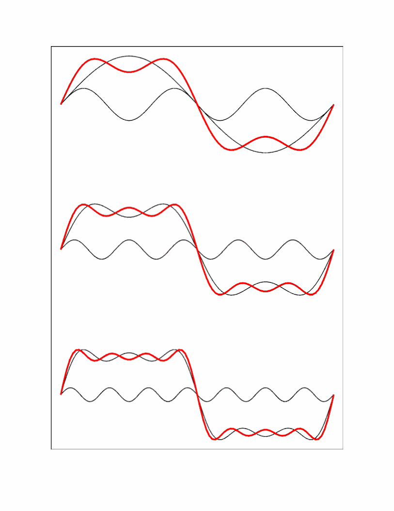
Occasionally, transformer manufacturers specify center-tapped secondaries in a slightly different manner. The transformer would be specified as follows: "Primary, 117 vAC 60 Hz. Secondary, 25 - 0 - 25 vAC @ 500 milliamperes." This means there are 25 volts from each side of the secondary to the center-tap or 50 volts across the entire secondary. The current rating is given for a type of rectifier known as a full-wave center-tapped rectifier, the two halves of the secondary are effectively in parallel and the current is doubled. Transformers used with vacuum tubes are more likely to be specified in this way because they are most likely to be used with a full-wave center-tapped rectifier.
Electrical Isolation.
It is possible to design equipment which can cope with the full voltage of the AC power line, thus eliminating the need for a transformer. However, transformers serve another purpose as important as changing the voltage. That purpose is to provide isolation of the circuit from the power line.
The argument might be made that one side of the 120 vAC line is connected to earth ground and no isolation is necessary. If a wiring error caused the leads to be reversed, the chassis of the instrument would be at a potential of 120 v with respect to earth ground. Such a wiring error did occur at the university I recently retired from. No one was injured but there was some soiled armor. It could be most unhealthy for anyone who might be unlucky enough to complete the circuit to ground.
In addition to safety considerations there are other reasons for not wanting a piece of equipment to be connected to the power line ground. The chief reason is noise. Noise is any electrical voltage or current in a place where it is not wanted. Noise voltages and currents are the weeds of electronics. In addition to bringing us the electric power we need, the power line brings us a lot of noise. One of the most effective noise removers is a transformer. The noise on a power line often has the same phase on both wires and, therefore, will not produce a magnetic field in the primary winding of a transformer. This is called common mode noise and will be discussed in more detail in the section on differential amplifiers.
In laboratories, recording studios, and radio stations, many different pieces of equipment are connected to work together. If each piece of equipment has its own earth ground and is connected to another piece of equipment, a phenomenon known as "ground-loop noise" appears. There are two possible solutions to this problem. One is to connect each piece of equipment to earth ground and make sure there is no electrical ground connection between individual pieces of equipment. The other is to connect only one piece of equipment to earth ground and make sure that there is only one ground wire from that piece to each of the other pieces of equipment in the setup. The isolation provided by the power transformer is absolutely vital to this "single point" grounding system.
3.4 Semiconductor Diodes.
Before we can discuss rectifier circuits it is necessary to understand the semiconductor diode. An ideal diode is a device which will conduct current in one direction only. When current flows in the forward direction, the resistance of the diode is zero, the voltage drop is zero. When current attempts to flow in the reverse direction it encounters an infinite resistance. Absolutely no current will flow and the voltage can build up to any value demanded by the circuit. As with all other ideal things, the ideal diode does not exist in the real world but real diodes come close enough to be most useful.
Unfortunately, there is insufficient space here to cover the physics of semiconductors in detail. Whole books 1 have been devoted to this topic and there is a course in this department entitled "Solid State Physics" which interested students should enroll in. Meanwhile, we can only scratch the surface. Emphasis will be placed on visualization of the physical processes which are taking place.
Semiconductor Devices and Applications 1 by R. A. Greiner McGraw-Hill 1961
A Semiconductor Is a Semiconductor Is a Semiconductor.
A semiconductor is not a very good conductor nor is it a very good insulator. It is a semiconductor. Two examples of semiconductor material are silicon and germanium.
Silicon and germanium each have 4 valance electrons in an outer shell which has room for 8 electrons. These elements (and carbon as well) form very stable tetrahedral crystals with the shared valance electrons filling the outer electron shell of each atom. If every electron stayed in place within the crystal lattice the crystal would be a perfect insulator. The electrons do not stay home.
Figure 3.3 Energy Diagram of a Semiconductor Material.
For a verbal description click here.
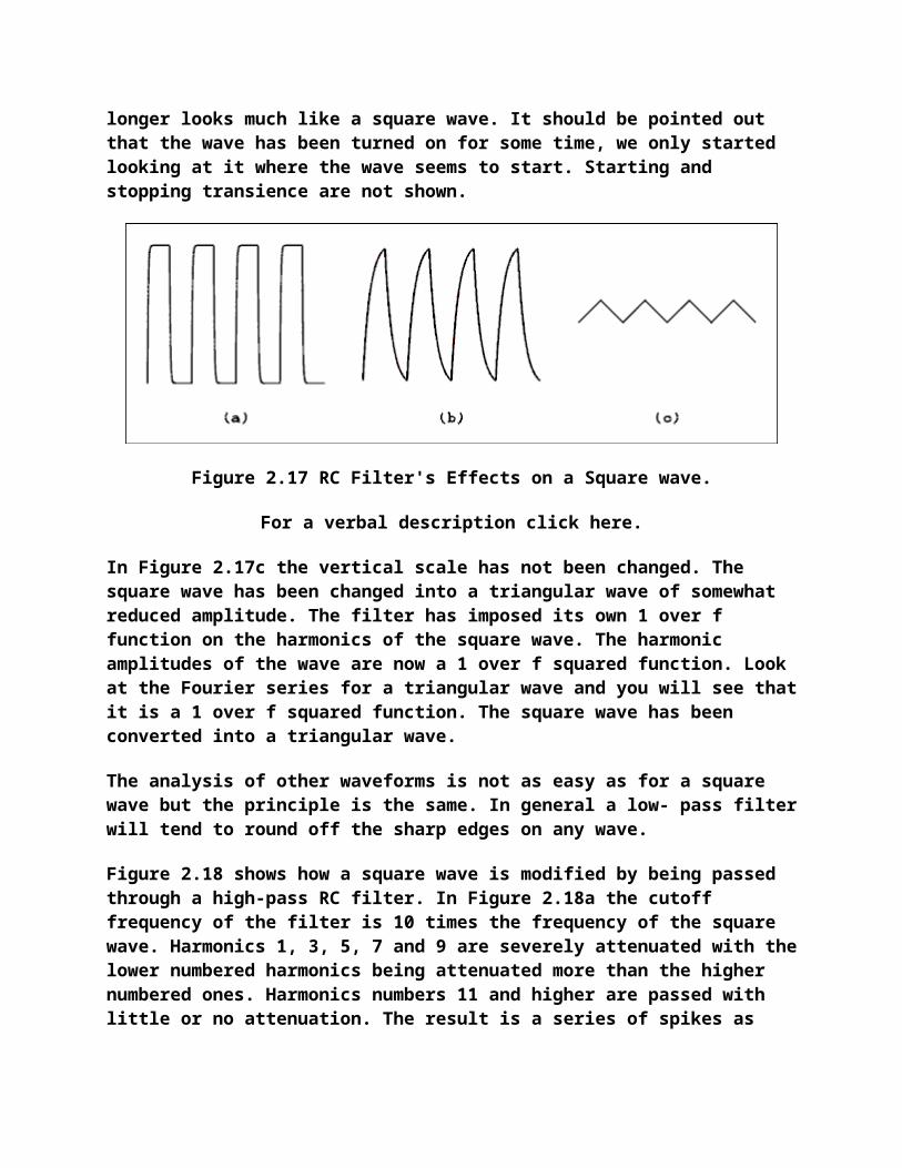
Figure 3.3 shows the possible energy levels for the electrons in a semiconductor crystal. When the electrons have a low energy level, they are in the valence energy band. Electrons which fall within this energy band will be bound to their particular valence bond. If an electron is given enough energy to jump over the forbidden energy band and enter the conduction band, it is set free from the valence bond and can move through the crystal.
The width of the forbidden band is called the band-gap energy. The band-gap energy for silicon at room temperature (300 degrees K) is 1.106 electron-volts (ev) and for germanium it is 0.67 ev. At room temperature there is enough thermal energy in the crystal lattice to promote some electrons to the conduction band.
Holes and Electrons.
Electrons which are in place in the lattice are in the valence energy band. Due to normal thermal agitation an electron can gain enough energy to move into the conduction band and leave its place in the lattice to become a conduction electron. An electron which has been promoted into the conduction energy band is free to move through the crystal under the influence of an electric field. But there is more to conduction in a semiconductor than conduction electrons.
When an electron leaves its place in the crystal lattice it leaves behind a hole in the lattice. Strange as it may seem, the hole does not stay in place but moves as if it were a positively charged particle. It has energy and even momentum. A hole can move by a nearby valence electron jumping from its place in the crystal lattice to the hole without entering the conduction energy band. After the electron has jumped, it leaves a hole where it used to be. Thus, the hole can move through the crystal lattice.
Thermal energy in the crystal lattice creates hole- electron pairs which move through the crystal. If there is an electric field present, the electrons will move toward the positively charged region and the holes will move toward the negatively charged region. If there is no electric field present, the holes and electrons will move randomly.
If you visualize a crystal of silicon warming up from absolute zero, hole-electron pairs will begin to form. This process cannot continue indefinitely or the crystal would come apart because all of its valence bonds would be broken. When holes and conduction electrons (electrons not held in a valance bond) become plentiful enough, electrons will begin to fall into holes they happen to run into. This process is called recombination and goes on at the same rate as hole- electron pair formation. The equilibrium between pair formation and recombination causes silicon and germanium crystals to be semiconductors at room temperature.
In pure semiconductor material the concentration of holes is the same as the concentration of electrons in the conduction band. (The total number of electrons cannot change, what we mean when we talk about changing the concentration of electrons, is the number of electrons which are free for conduction.) In pure silicon or germanium
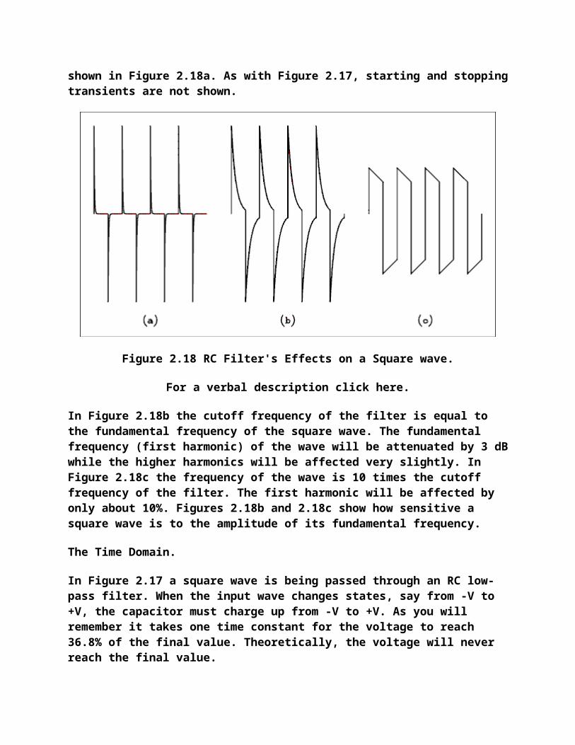
Ne = Nh = KS T(3/2) (3.1) where Nh is the concentration of holes, Ne is the concentration of electrons in the conduction band, KS is a constant which must be determined experimentally and T is the Kelvin temperature. The value of KS is 4.74 x 10²² for silicon and 1.76 x 10²² for germanium. Ne and Nh have units of 1/m2.
We may now define the intrinsic charge carrier concentration ni as
Ni = KS T(3/2) (3.2) Equations 3.1 and 3.2 say that the charge carrier concentration is quite temperature dependent. Equation 3.2 defines the pure semiconductor or intrinsic charge carrier concentration.
Changing the Relative Concentration of Holes and Electrons.
Now suppose that we deliberately add some impurities to a crystal of pure semiconductor such as silicon. We are not going to just throw in some dirt from the floor; we will carefully control what goes in and how much.
If we add an element from group 5 in the periodic table the effect on a semiconductor is striking. The elements from group 5 have five electrons in the outer shell. Wherever one of these atoms appears in the crystal lattice, four of its outer electrons go into valence bonds and the fifth one becomes very loosely bound to its atom. A very small amount of energy (about 0.05 ev) is needed to promote this electron into the conduction band. Such an impurity is called a donor impurity because each atom donates an electron to the conduction energy band.
If we go back to pure silicon and add an element from group 3 in the periodic table the effect on a semiconductor is opposite to that for an element from group 5. The elements from group 3 have three electrons in the outer shell. Wherever one of these atoms appears in the crystal lattice, there are only three electrons in the outer shell to go into valence bonds. The unfilled valence bond is a hole. Once a wandering electron has fallen into this hole, a comparatively large amount of energy is required to promote that particular electron back into the conduction energy band. That electron and its three companions will remain in place and a hole will have been set free to wander through the crystal lattice. Such an impurity is called an acceptor impurity because each atom accepts an electron from the conduction energy band and causes a conduction hole to be created.
When a donor impurity loses its loosely-bound electron or an acceptor impurity captures a wandering electron (loses its loosely-bound hole), the impurity atom is said to be ionized. Ionization in a solid means the same thing it means in a liquid or gas, the loss of, or gain of an extra electron. When an impurity is added to a semiconductor, most of the impurity atoms are ionized most of the time, statistically speaking.
Because the impurity atoms are virtually 100 percent ionized, for every atom of donor impurity there is an additional electron in the conduction band. For every acceptor atom
added, there is an additional conduction hole in the crystal. The meaning in this discussion is that donor impurity is added to one piece of semiconductor and acceptor impurity is added to another piece of semiconductor.
Recombinations occur when wandering holes and wandering electrons happen to collide. The probability of collisions goes up as the concentration of either holes or electrons goes up. When, for example, a donor impurity is added to a semiconductor, the increased concentration of electrons causes more frequent collisions and a higher rate of recombination. The recombination rate falls again when the hole concentration has been reduced to the point where a new equilibrium has been established. The end result is to decrease the concentration of holes in the crystal. It can be shown mathematically, in about ten pages, note 1, that
Ne Nh = ni2 (3.3)
where Nh is the concentration of holes, Ne is the concentration of electrons and ni is as defined in equation 3.2. Because the impurity atoms are completely ionized, the concentration of electrons is equal to the concentration of donor atoms Ne = Nd and for acceptor impurity Nh = Na where Nd and Na are the concentrations of donor and acceptor impurity atoms respectively. Thus it is possible to write for a semiconductor which has been "doped" with a donor impurity
Ne = Nd N and h = ni2 / Nd (3.4)
and for a semiconductor "doped" with an acceptor impurity Nh = Na N and e = ni
2 / Na (3.5)
Some Terms to Be Remembered.
As you may have guessed the process of adding impurity atoms to a semiconductor crystal is called doping. A semiconductor which has been doped with a donor impurity has many more negative charge carriers than positive charge carriers. This is known as N (negative) type semiconductor. A semiconductor which has been doped with an acceptor impurity has many more positive charge carriers than negative charge carriers. This is known as P (positive) type semiconductor.
There are two types of charge carriers, holes and electrons. A majority carrier is the type of carrier which there are more of in a particular type (P or N) of semiconductor. A minority carrier is the type of carrier which there are fewer of in a particular type (P or N) of semiconductor.
Example 3.2
Identify each of the following as majority or minority carriers: (a) electrons in N type semiconductor, (b) holes in P type semiconductor, (c) electrons in P type semiconductor and (d) holes in N type semiconductor.
Solution:
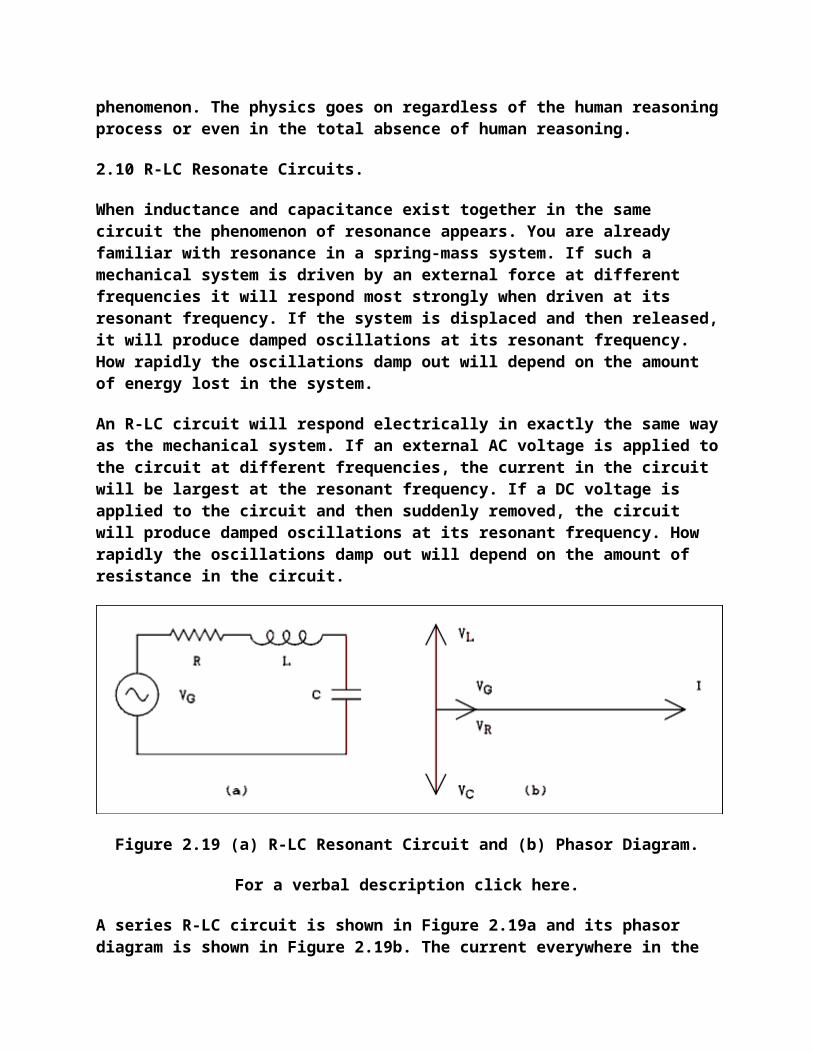
The majority carriers have the same charge polarity as the type of semiconductor in which they are found. The one which is left is the minority carrier. Thus, (a) majority, (b) majority, (c) minority and (d) minority.
The P-N Junction
Figure 3.4a shows a schematic representation of two blocks of semiconductor material. The block on the left is N type and the dots represent conduction electrons. The block on the right is P type and the circles represent the conduction holes. The concentration of minority carriers is so small as to be negligible at room temperature. In Figure 3.4b the two blocks of semiconductor material have been placed in physical contact. * As soon as contact has been established, the normal wanderings of charge carriers due to thermal agitation will cause some charge carriers to cross the junction. As soon as a carrier crosses the junction it
Figure 3.4 "Making" a P-N Junction Diode
For a verbal description click here.
becomes a minority carrier. The probability of colliding with a carrier of opposite sign is very high and the wanderer will soon disappear by recombination with a carrier of opposite sign. There is a net movement of charge across the junction with electrons moving to the right and holes moving to the left. The departed electrons on the left leave behind the ionized donor impurity atoms which have a positive charge. The departed holes on the right leave behind the ionized acceptor impurity atoms which have a negative charge. That places an electric field across the junction, which is positive on the left and negative on the right. This electric field eventually builds up to such a value as to prevent any more electrons from moving to the right or holes from moving to the left across the junction. The graph in Figure 3.4b indicates the electric potential within the block of semiconductor material. The electric potential comes to zero at each end of the block; if it did not, we would have a cheap source of electricity.
This is not how P-N junction diodes are manufactured. * In fact, this could not even be done in the laboratory.
This is merely a thought experiment which illustrates how the depletion region and contact potentials are formed in a P-N junction.
The region near the junction becomes depleted of charge carriers in the conduction band. As stated above, there are ions in the depletion region but these ions are held in the crystal lattice and are not in the conduction energy band. The depletion region constitutes an insulator and the regions on either side of the depletion region which are not depleted of charge are conducting regions. This concept is very important. Failure to understand the depletion region will result in failure to understand how P-N junctions conduct in only one direction.
Animation, which is not possible in a paper book could not be done in any medium when I was teaching this subject. We have sure come a long way baby.
Figure 3.4c Animation showing Figure 3.4a and 3.4b in action.
For a verbal description click here.
When the two pieces of semiconductor touch, the electrons from the N side and the holes from the P side start to randomly wander across the junction. The animation shows holes and electrons making a beeline toward their opposite number on the other side. Randomness is much harder to do in animation so the much easier straight line path was taken. It cannot be over emphasized that when electrons and holes meet and mutually annihilate, nothing is being destroyed. The electrons remain in existence but their energy level has been reduced so they are no longer in the conduction energy band. The electron filled a hole so it no longer exists but it was never their in the first place.
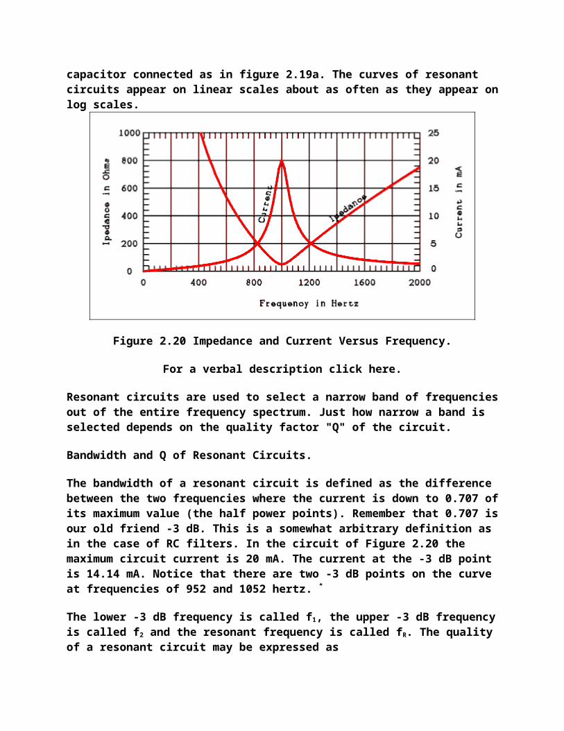
Figure 3.5 Reversed and Forward Biased P-N Junction
For a verbal description click here.
Figure 3.5a shows a P-N junction with an external battery connected in such a polarity as to increase the potential across the junction. The effect of this is to increase the width of the depletion region and increase the potential across the junction. Notice that the positive terminal of the battery is connected to the N type semiconductor and the negative terminal of the battery is connected to the P type semiconductor. This condition is known as reverse bias. Under normal conditions no appreciable current will flow through a reversed biased P-N junction. It is true that minority carriers on the left (holes) are moving to the right across the junction and minority carriers on the right (electrons) are moving to the left across the junction. In modern P-N junction diodes this minority carrier current is so small that an electrometer is required to measure it.
Figure 3.5d Figure 3.5a in action.
For a verbal description click here.
In the animation it appears that the electrons on the left and the holes on the right are being absorbed by the end lines. On the left the electrons are being absorbed into the copper wire that makes contact with the semiconductor and sucked into the positive terminal of the battery. On the right there are electrons coming from the negative terminal of the battery and fed into the semiconductor. At the point of contact between the semiconductor and copper, electrons are combining with holes. The current will flow only when the voltage is changing. This is like a capacitance and is called the "charge storage capacitance", or "charge storage effect", of the diode.
The depletion region constitutes an insulator and the regions where there are charge carriers in the conduction energy band are conductors. This forms a capacitor. As the voltage changes the width of the depletion region changes, changing the amount of capacitance. Any P-N junction will show varying amounts of capacitance as the reverse voltage is changed. In rectifiers and small switching diodes this is only a few picofarads. Special diodes are available that have enhanced capacitance and are known as variable capacitance diodes or varicaps for short.
Figure 3.5b shows a P-N junction which is slightly forward biased. The first few tenths of a volt only serve to reduce the potential gradient across the junction and no conduction results. In Figure 3.5c the forward bias has been increased to the point where the contact potential has been overcome. The width of the depletion region has been reduced to zero, and current now flows in the forward direction. Notice that the positive terminal of the battery is connected to the P type semiconductor and the negative terminal of the battery is connected to the N type semiconductor. This condition is known as forward bias.
Figure 3.5e Figures 3.5b and c in action.
For a verbal description click here.
A forward biased P-N junction will conduct large amounts of current at a voltage drop of less than one volt. As the current is increased in the forward direction, the voltage increases logarithmically as shown in Figure 3.6.
Figure 3.6 Voltage Versus Current Curve of a P-N Junction
For a verbal description click here.
The reverse bias on a P-N junction cannot build up to infinity. As the reverse bias voltage is increased, the electric field across the junction becomes so great as to rip electrons out of
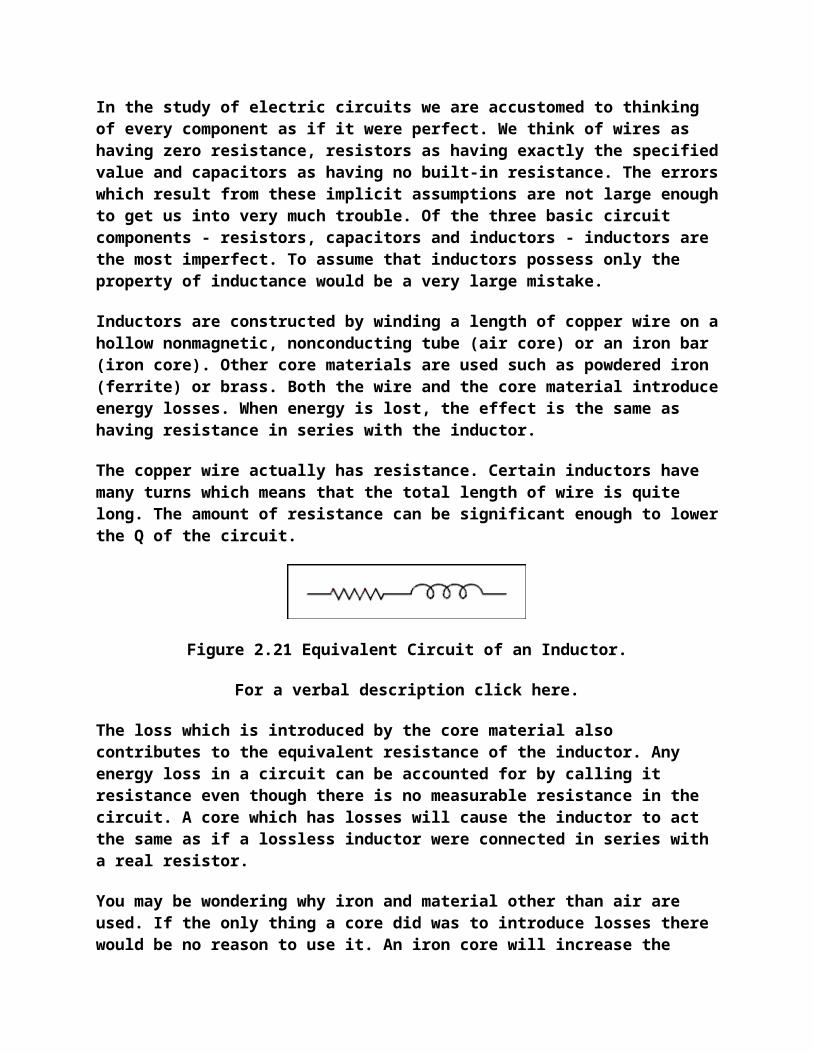
their valence bonds. The electric field imparts enough energy to valence electrons to promote them to the conduction energy band. The result is that we have a new source of conduction electrons. The newly freed electrons are accelerated to a high velocity and when they collide with other valence electrons, these valence electrons are also promoted to the conduction energy band. The current rises to a very large value and the voltage cannot rise any further. This condition is called avalanche breakdown but is sometimes mistakenly called Zener breakdown. Zener breakdown will be covered in a later section. Avalanche breakdown places a practical limit on how much voltage a P-N junction diode can withstand in the reverse biased direction.
A Derivation.
Get in touch with your inner physicist.
In the discussion above it was said that electrons from the N side of the junction will move towards the P side of the junction. We will call this current INN(0). The first subscript gives the polarity of the charge carrier and the second gives the type of semiconductor where the charge carrier originated. The "(0)" means with zero external bias applied. It can be shown that (note 1)
INN = INN(0) e-(eVd/kT) (3.6) and
IPP = IPP(0) e-(eVd/kT) (3.7) Under zero bias conditions there can be no net flow of holes or electrons across the junction; therefore,
INN = INP I and PP = IPN That is to say there is an equilibrium of charge carriers so that the number of minority electrons crossing from P to N is equal to the number of majority electrons crossing from N to P. The same goes for holes. This means that
INP(0) = INN(0) e-(eVd/kT) (3.8) And
IPN(0) = IPP(0) e-(eVd/kT) (3.9) The "e" in the exponent is the charge on the electron, Vd is the diffusion voltage, k is Boltzmann's constant and T is the Kelvin temperature. If an external bias Vj is applied, these equations become
INN = INN(0) e-e(Vd-Vj)/kT (3.10) And
IPP = IPP(0) e-e(Vd-Vj)/kT (3.11) With an external bias applied the total junction current is
IJ = holes from P to N + electrons from N to P
IJ = (INN + IPP) e-e(Vd-Vj)/kT - IPN(0) - INP (3.12) (0)
Combining this equation with equations 3.8 and 3.9 we have IJ = ( INP(0) + IPN(0) ) (eeVj/kT (3.13) - 1)
If we let IO = INP(0) + IPN(0) we have IJ = IO (eeVj/kT (3.14) - 1)
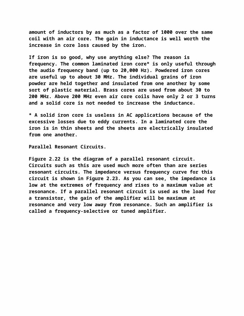
This is the "diode equation" and its derivation is obligatory in any discussion of semiconductor diodes.
For negative values of Vj (reverse bias) the limiting case is IJ = IO. IO is correctly called the reverse saturation current but is often called the reverse leakage current. For modern silicon P-N junction diodes the value of IO is of the order of 10-12 amperes.
For positive values of Vj the current will rise exponentially. Diodes are never used in circuits where the circuit determines the voltage. Diodes are used in circuits where the circuit sets the current and the diode itself is allowed to set its own voltage drop. With current as the independent variable the voltage rises logarithmically and will easily stay within realistic bounds.
3.4A Vacuum Diodes.
A Minute Amount of History.
Cold Cathodes.
The very first diodes were made by Crookes. They were glass tubes with a metal electrode in each end and a place to connect a vacuum pump. Crookes didn't remove all the air from the tube. He found that an electric arc could be maintained over a much greater distance if the pressure was reduced to somewhere in the range between 1/10 to 1/100 of atmospheric pressure. He was using voltages of thousands of volts. The only thing distinguishing the anode from the cathode was which was connected to the positive of the voltage source and which to the negative.
Roentgen became curious about what would happen if the pressure was pumped down to as low as possible. He found that the arc stopped, leaving a faint greenish-blue glow. Measurements revealed that some current was flowing through the tube. The florescent material used to make watch dials glow in the dark was known in Roentgen's time and he had some in his laboratory. He happened to notice that this material glowed more brightly when the tube was in operation. He moved it closer to the tube and found that it glowed even brighter. Evidently the sample was in the form of a flat plate. Most likely it was coated on a glass plate like those used for photography in that time. When he interposed his hand between the florescent plate and the tube he probably got the shock, non electrical, of his life. He could see the outlines of the bones in his hand as shadows on the plate. That was the discovery of x-rays.
What was happening was that the strong electric field was pulling electrons out of the metal of the cathode, negative electrode, and they were being accelerated to a very high velocity and then impacting the anode. The incoming electrons had so much energy that they knocked other electrons out of the inner shells in the atoms of the anode metal. These electrons were replaced by electrons from the outer shells falling down to replace them. These large energy transitions caused the atoms to emit electro magnetic radiation of a very short wavelength, namely x-rays.
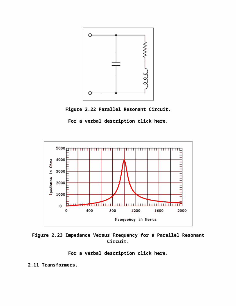
Hot Cathodes.
About this time Edison found that in a light bulb with two filaments, current would flow if the cold one was made positive with respect to the hot one but not if the polarity was reversed. He saw no use for this effect but noted it as curious.
It didn't take long for Roentgen and friends to put this discovery to use. They surmised correctly that a heated filament could emit electrons better than a cold piece of metal and the hot cathode was born.
Bulbs or Tubes?
All of this was taking place before 1900. You couldn't run down to your local Radio Shack and pick up a tube. If you wanted to experiment you had to make your own. The long slender tubes that were used by chemists were readily available but they couldn't resist pressure differences as well as a sphere. When it comes to blowing a glass bulb, a sphere was easier to form than a thin tube. That's why in those old pictures the devices are usually spherical bulbs rather than tubes. In fact writings from the early years of the 20th century in the united states refer to, what we would call a tube, as a bulb.
The Fleming Valve.
In England Fleming found that a device much like an x-ray tube, only much smaller, could be used to detect radio waves. He visualized it as working like a water valve but for electrons. It was called "The Fleming Valve" and to this day British techies and tinkerers call them electronic valves.
So What's a Diode?
The name diode comes from the Greek for two. Diodes have two elements, a cathode and an anode. The simplest diodes, and in fact the earliest ones, have a cathode which consists of a filament that can be heated to red or even orange hot by passing an electric current through it. The anode is a flat metal plate, often called the plate.
Thermeonic Emission.
Before we can understand thermeonic emission of electrons from a metal surface we need to understand how electrons behave inside a metal. Before we can understand how electrons behave inside a metal we must understand how electrons behave inside a nonmetallic solid. So here we go.
The atomic model proposed by Niels Bore is now considered hopelessly out of date. It is ridiculed by modern physicists but it is still a useful tool in understanding atoms for those who aren't going to get a PhD in the subject. The nucleus of the atom is positively charged and the negatively charged electrons spin around it a bit like the planets around the sun. It's a case of forces in balance like the solar system. The inner electrons are held very
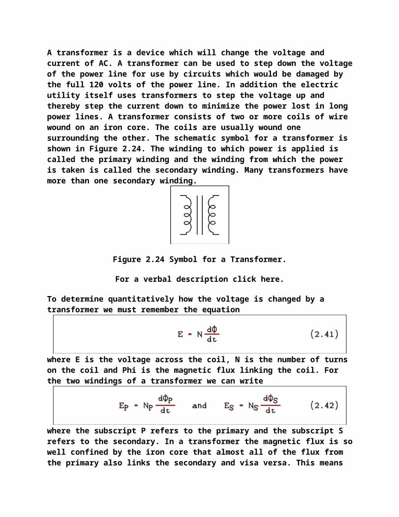
tightly and it takes a lot of energy to pull them out of orbit. The outer most are more loosely held and it doesn't take a lot of energy to pull them away from the nucleus.
At this point our solar system model starts to fall apart because an atom has things called shells. There is a maximum number of electrons that can exist in one shell. The innermost shell can hold up to 2 electrons, the second 8, the third 8, the fourth 18, the fifth 18 and the sixth 32. If the outermost shell is completely filled the atom is very unreactive, a kind of loner. These are the inert gases which refuse to form any sort of bonds with any other element. Carbon has its outer shell, which will hold 8 electrons, half filled. When several atoms of carbon get together they form very stable bonds with each other by sharing their outer electrons to make each atom feel as if its outer shell is completely filled. This is how diamonds are formed.
Many compounds are formed by sharing electrons in a partially filled outer shell. These are called covalent compounds. The bonds that hold the molecules together are known as covalent bonds. Some other compounds are formed by one, or sometimes two, electrons jumping from an atom of one element to an atom of another element. For example common table salt, sodium chloride, is formed when atoms of sodium give up the loan electron in their outer shells to an atom of chlorine which needs only one electron to fill its outer shell. The resulting positive and negative ions have a strong attraction for each other. These are known as ionic compounds.
If you could have a single atom of any element in isolation you would find that it takes a certain amount of energy to remove one electron from its outer shell. This energy varies considerably from element to element. Some need very large amounts of energy and others need much less. It always takes some energy to take an electron away from an atom in isolation.
When atoms of the same kind are clustered together, as is always the case, things change. In elements classed as metals the amount of energy required to remove an electron from its atom is zero. That's because the atoms are so close together that the electrons in the outer shells don't know to which atoms they belong. They all just wander around in there, moving randomly. If an electric field is applied externally the electrons will move in the direction the field wants them to and we now have an electric current in the metal. When there is no external field the movement is completely random.
All of these randomly moving electrons don't have the same velocity. There is a statistical value which depends on the temperature but some are faster, some are slower, and a very few are very fast. If one of these high speed electrons comes to the surface of the metal it can pass through the surface and leave the metal behind. If this happens many times the metal will develop a positive charge and subsequent would-be escapees will be attracted back to the surface.
When electrons escape from the surface of a metal it is called electron emission. If we set up a source of EMF and arrange things so the escaped electrons will be collected and the positive charge on the emitting metal is neutralized by the continuous replacement of
electrons the process of electron emission will continue until the EMF source is removed. If the emitting metal is at room temperature the process is called cold emission. A very strong electric field is required to produce any significant current from cold emission. That means a high voltage applied between electrodes that are close together.
The piece of metal that is connected to the negative of the EMF and emits the electrons is called the cathode. The one that is connected to the positive and collects the electrons is called the anode. I am told that these names come from the Greek words for up and down but I couldn't begin to tell you which is which. It's all Greek to me.
Edison used to make experimental light bulbs with more than one filament to save work for his glass blowers. As related briefly above he found that conventional current would flow from a cold filament to a hot one but not the other way. This became known as the Edison effect. I don't think the existence of electrons had been recognized at this time. Conventional current flows opposite to electron current. This may well have been one of those serendipitous discoveries that seemed to occur often in early science.
As the temperature of the cathode is increased the electrons get to moving much faster than at room temperature. The likelihood of one having enough velocity to escape from the surface is tremendously increased. Hot emission does not require a strong electric field and will occur even in the absence of one. That can't go on very long because of the positive charge that develops on the cathode but it will build up a considerable space charge in an evacuated chamber. A space charge is a volume that has a lot of electrons floating around in it.
The carbonized filament that Edison used was not a very good emitter of electrons. The later tungsten filaments weren't either. Very early tubes used tungsten because that was all that was known. They glowed as bright as light bulbs. It was soon found that if a little thorium was alloyed with the tungsten the filament didn't need to run as hot and would still emit more electrons per square millimeter of filament surface. These are used to this day in transmitting tubes. They glow about the same color as the upper part of a candle flame.
The most efficient emitter is an oxide coated cathode. The discovery of this process made possible the heater-cathode type of tube. The electrical cathode is a small cylinder with the heater inside and electrically insulated from it. The heater is actually a filament but it is not the electrical cathode of the tube. Providing electrical insulation and thermal conductivity at the same time is not an easy thing to do. (The same battle is still being fought to provide cooling for transistors and microprocessors.) The end result is that the heater must be hotter than the cathode. If the cathode were thoriated, the heater would have to run so hot that it would not last long. In a heater-cathode tube the heater runs about the same temperature as a thoriated tungsten filament. The cathode runs a dull red but you can't see it in most tubes. The 6AS7G/6080WA has a gap in the plate and the grid wires can be seen. The cathode is visible between the grid wires and you need a fairly dark room to see its glow. Electrically separating the cathode from the heater had the effect of making circuits mor simple and meant that AC could be used to heat the tubes without inducing much hum in the signal path.
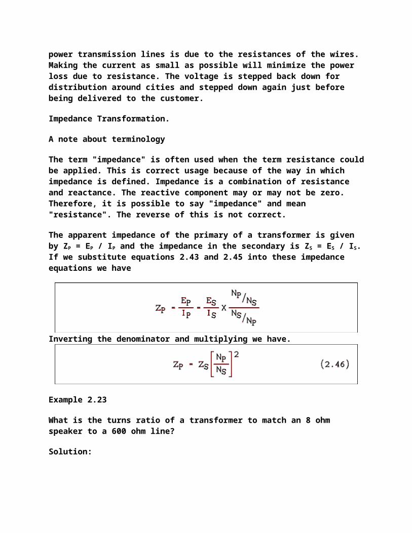
The hot cathode emits electrons in droves. Many more than are needed. They build up in the volume around the cathode and form a large pool of electrons just waiting for something positive to happen. This pool of electrons is called the space charge. When the anode (plate) is made positive some of the electrons are attracted to it. They impact on it, are absorbed into the metal and electrons flow out of the plate connection into the battery or what ever provided the positive voltage. The other end of the voltage source must be connected back to the cathode in some way.
If the polarity is reversed which makes the plate negative with respect to the cathode the electrons in the space charge are repelled away from the plate and no conduction takes place. The plate is cold and is made of a metal that is a very poor emitter of electrons. The voltages are not nearly as high as those used by Crooks so there is no cold emission from the plate. This makes the diode conduct current in only one direction.
Rectification.
Diodes can only do two basic things. These are 1) generate x-rays, and 2) rectify. Not many of us are interested in generating x-rays so let's talk about rectification.
The Space Charge.
The cathode of a tube is coated with a very special oxide that emits electrons very easily. It can readily be damaged by operating above or below the proper temperature or by being "poisoned" by the residual air in the tube. The space charge serves another vital function. There is no such thing as a perfect vacuum. In fact the space in near earth orbit is a better vacuum than can be made on the surface of earth. Farther out in space the vacuum is even better. What this means is there are lots of air molecules running around inside of a vacuum tube. The space charge protects the cathode from these air molecules. Some of these molecules lose an electron and become positive ions. They are attracted to the negative cathode and if it weren't for the space charge they would impact on the surface of the cathode doing considerable damage. Over time the ability of the cathode to emit electrons would be seriously impaired rendering the tube useless. As these ions run through the space charge they gain electrons from the many collisions and become negative ions. Their direction is reversed turning them away from the delicate cathode.
Indirectly heated cathodes.
Most vacuum tubes have a basically cylindrical configuration. Figure two shows how a filament (directly heated) cathode type diode differs from a heater (indirectly heated) cathode type diode.
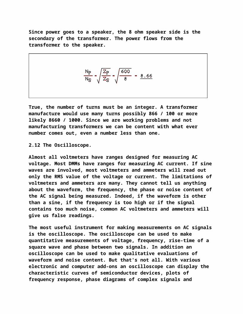
Figure 3A.1 Construction of vacuum diodes.
For a verbal description click here.
In the filament type diode the cathode is usually a single wire running down the center of the cylindrical plate. In the heater type diode the filament is called the heater because that is its function. It is surrounded by a material which is an electrical insulator and a thermal conductor. The best known material having those properties is mica although aluminum oxide is most often used between heater and cathode. Outside of the electrical insulator is the cathode which is a cylinder with the special coating on the outside. The reason for having both types of tubes will be explained below.
Rectification.
The most important use of diodes is as a power rectifier. Rectification is the name given to the process of changing AC to DC. The process of detecting a radio signal also involves rectification. However, this process is more often called detection. The term rectification is reserved for power supply usage. Diodes are occasionally used for clamping, preventing a voltage from going above or below a given value, or clipping, preventing an audio signal from exceeding some preset level by knocking off the peaks. But by far the most common use of diodes is as rectifiers. The property of a diode that makes all this possible is its unidirectional conditivity.
Figure 3A.2 Forward and reverse connection of a vacuum diode.
For a verbal description click here.
Figure 3A.3 shows a directly heated cathode, filament, diode connected as a rectifier. As you can see from the wave forms this does not give the steady DC you are used to thinking of. For details about rectification and filtering see other sections of Chapter 3 of this book..
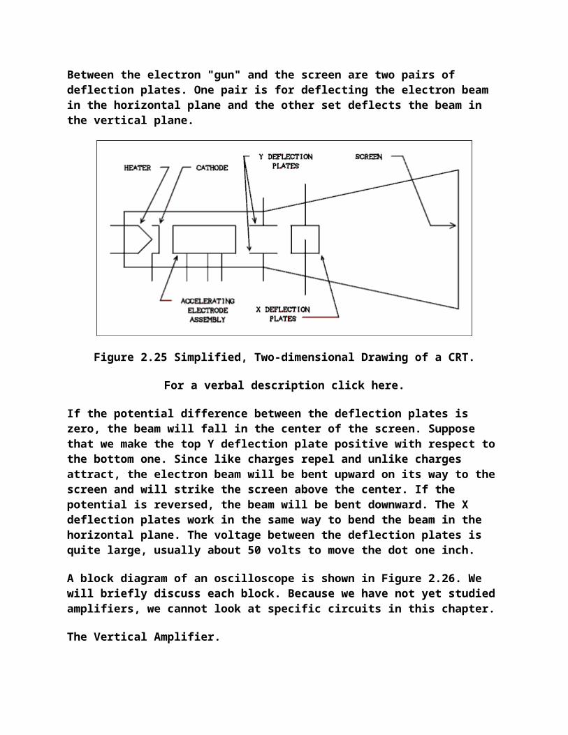
Figure 3A.3 Filament type diode used as a rectifier.
For a verbal description click here.
The entire filament and its supply winding are at a potential of several hundred, or even several thousand, volts above ground. The typical filament supply voltage is 5 volts so the difference has little effect on the operation of the diode. When I was a novice I used to wonder why all that voltage didn't burn out the 5 volt filament. What matters to the filament is the voltage from one end of it to the other end. If one end of the filament is at 350 volts and the other end is at 355 volts the only voltage to effect the filament is the difference of 5 volts. Consider this point carefully. It's VERY important that you understand it. If you don't understand, stop and think about it. Don't go on until you do. If you need to, email a question to me. I am the teacher in this class and answering questions is what I'm here for.
The disadvantage of a filament type rectifier, as compared to an indirectly heated cathode type, is that it requires a separate winding on the transformer or in big transmitters a separate transformer for the filament. The advantage is that the maximum voltage is limited only by the plate to filament insulation within the tube and the insulation in the filament transformer.
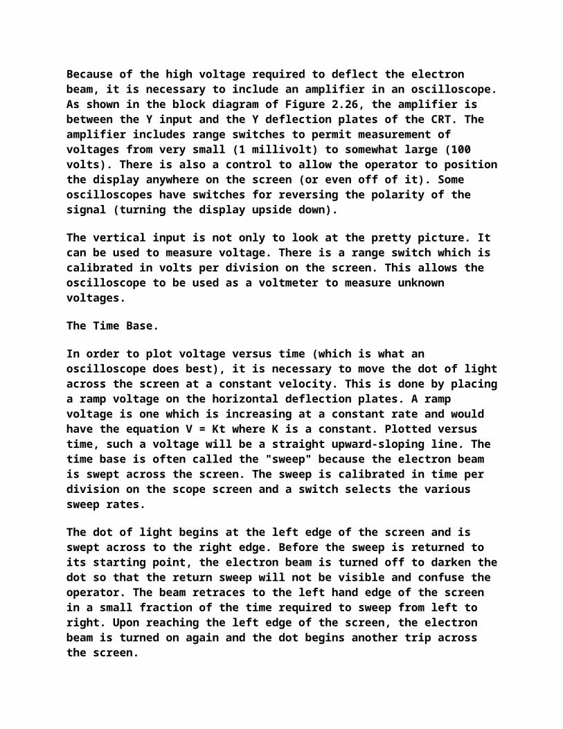
Figure 3A.4 Heater type diode used as a rectifier.
For a verbal description click here.
Figure 3A.4 shows an indirectly heated cathode type diode being used as a rectifier. Its heater can, and usually does, operate from the same voltage supply as the rest of the tubes in the device. Note that the heater winding is shown grounded. Also note that there is only one heater winding instead of two as in Figure 3. The insulation between the heater and cathode must withstand the full output voltage of the power supply. The best tube manufacturers were able to do was about 500 volts. Filament type diodes can be used to rectify thousands of volts.
Detection
The tubes used as power supply rectifiers are not the ones you would use for detection of radio waves. In the crystal set described else where on this site you could replace the crystal diode with a small tube such as a 6AL5 or 6H6. These tubes used as detectors may be referred to as thermeonic diodes, Fleming valves, or detector tubes. But whatever they are called they work just the same.
How I got hooked.
My lifelong addiction began, not with the building of a crystal set, but upon seeing an animated film on early TV showing how vacuum tubes worked. In my continuing attempts to pass on my addiction here is an animated picture showing the electrons in a diode serving as a rectifier. The voltmeter on the left is measuring the instantaneous voltage of the AC input to the rectifier. The voltmeter on the right shows the pulsating DC across the
load resistor. You can see the electrons in the tube being attracted to the plate when it is positive and being repelled back to the filament when the plate is negative.
Figure 3A.5 animation of a rectifier in action.
For a verbal description click here.
Linearity.
Just as semiconductor diodes are non linear, the same is true of vacuum diodes. I'll spare you the derivation of the equation. Those who are interested are referred to the electrical engineering books used by their forbearers. The equation for the current in a vacuum diode is,
I = 2.335 x 10⁻⁶ A V3/2 / d2 (3A.1) Where V is the voltage between cathode and plate, A is the cathode area, and d is the distance between plate and cathode. The area term is why high current rectifier tubes such as the 5U4 are bigger than RF detector diodes such as the 6AL5.
When a vacuum diode is used as a detector, where linearity is necessary, the current is set to a small enough value so the V term will not become significant compared to the input AC voltage. Below is a plot of this equation were A = 0.001 square meters and d = 0.00125 meters.
Figure 3A.6 I-V Curve of a Fictitious Power Rectifier Tube.
For a verbal description click here.
The values were estimated from a 5U4 and based on tube manual data I think I am in the general ballpark but don't use this curve to predict the behavior of a real 5U4 in a real circuit.
In power supply circuits the nonlinearity doesn't make a bit of difference. The only goal is to allow current to flow in one direction and a bit of nonlinearity doesn't matter.
3.5 Rectifier Circuits.
A diode, whether vacuum or semiconductor, conducts current in only one direction. At typical current values the forward voltage drop of a semiconductor diode is 0.7 to 1 volt while the drop across a vacuum diode is typically 25 to 150 volts.
This large disparity in forward voltage drop means that a power supply must be designed to use either tube or semiconductor diodes and you can't change later. There are still some of those so called "solid state tube replacements" floating around. DON'T USE THEM! Installing them in existing equipment can result in 100 volts or more of additional B+ and you can do serious damage to what ever you put them in. I have nothing against the use of semiconductor diodes as long as the circuit has been designed for them.
It is the function of a rectifier to change AC to DC. In single phase circuits the rectifier changes the AC to a pulsating DC and some additional circuits are needed to change the pulsating DC to a smooth DC. In this section we will look at a few rectifier circuits.
The schematic symbol for a P-N junction diode is a triangle with a line across its point as shown in Figure 3.7. The triangle is the P side and the line is the N side of the junction. The P side is called the anode and the N side is called the cathode. Conventional current will flow in at the anode and out at the cathode. Current will flow in the direction of the arrow. Current will not flow from cathode to anode. Electron current flows in the opposite direction as conventional current. When current is flowing in the forward direction, the anode is more positive than the cathode by about 0.7 volts. If the cathode is positive with respect to the anode, no measurable current will flow and the voltage can have any value up to the rated maximum PIV (peak inverse voltage) or PRV (peak reverse voltage) of the diode. Typical silicon diodes have PIV ratings in the range of 50 to 1000 volts. Vacuum diodes of the type found in consumer equipment may have PIV ratings from 350 to 1500 volts. Rectifier tubes designed for use in high power transmitters may have PIV ratings in the thousands of volts and maximum currents in Amps.
These drawings are being used because they already exist. When vacuum rectifiers are used the circuits aren't any different. Just substitute a vacuum diode for the semiconductor diode shown and provide power for the filament or heater.
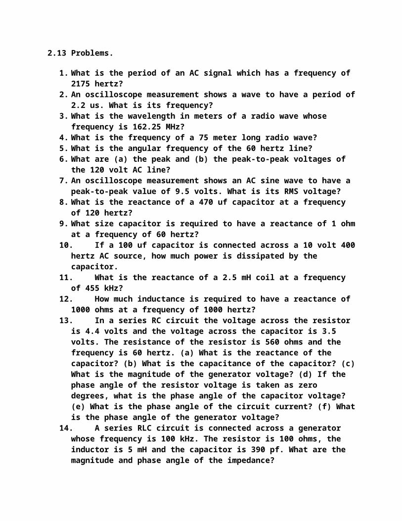
Figure 3.7 Half-wave Rectifier.
For a verbal description click here.
The circuit of a half-wave rectifier is shown in Figure 3.7 above, along with its output waveform. When the top end of the transformer secondary is positive with respect to the bottom end, current will flow from the anode to the cathode of the diode. The forward drop across the diode is small compared to the voltage of the transformer and almost all of the voltage appears across the load resistor. The positive half-cycle appears across the load. When the top end of the transformer secondary is negative with respect to the bottom end, current will not flow through the series combination of the diode and load resistor. If there is no current through the load resistor, there can be no voltage drop across it. The voltage of the transformer secondary is dropped across the diode and does not appear across the load resistor. Thus we have only half of each cycle appearing across the load. This should be called half-cycle rectification but it was named in the early years of electricity (prior to 1920) when people were not as careful with their terminology as we are today. The process which is going on in Figure 3.7 is called half-wave rectification and the circuit is called a half-wave rectifier.
Figure 3.8 Full-wave Center-tapped Rectifier.
For a verbal description click here.
Figure 3.8, above, shows the circuit and output waveform of a full-wave rectifier. You will note that the pulsations occur twice as often in Figure 3.8 as they do in Figure 3.7. A higher rate of pulsations is easier to smooth out. It is for this reason that a half-wave rectifier is very rarely used. Figure 3.8 is called a full-wave center-tapped rectifier circuit. A transformer with a center-tapped secondary is required to construct this circuit. The two diodes and the two halves of the transformer work alternately. They can handle twice as much current as either one working alone.
On the first half-cycle when the top end of the secondary is positive with respect to the center-tap the bottom end is negative with respect to the center-tap. (Note that the load is returned to the center-tap, not to the bottom of the secondary.) Diode D1 is forward biased and D2 is reversed biased. D1 conducts current which flows through the load and back to the center-tap. The first half-cycle appears across the load with the top end of the load
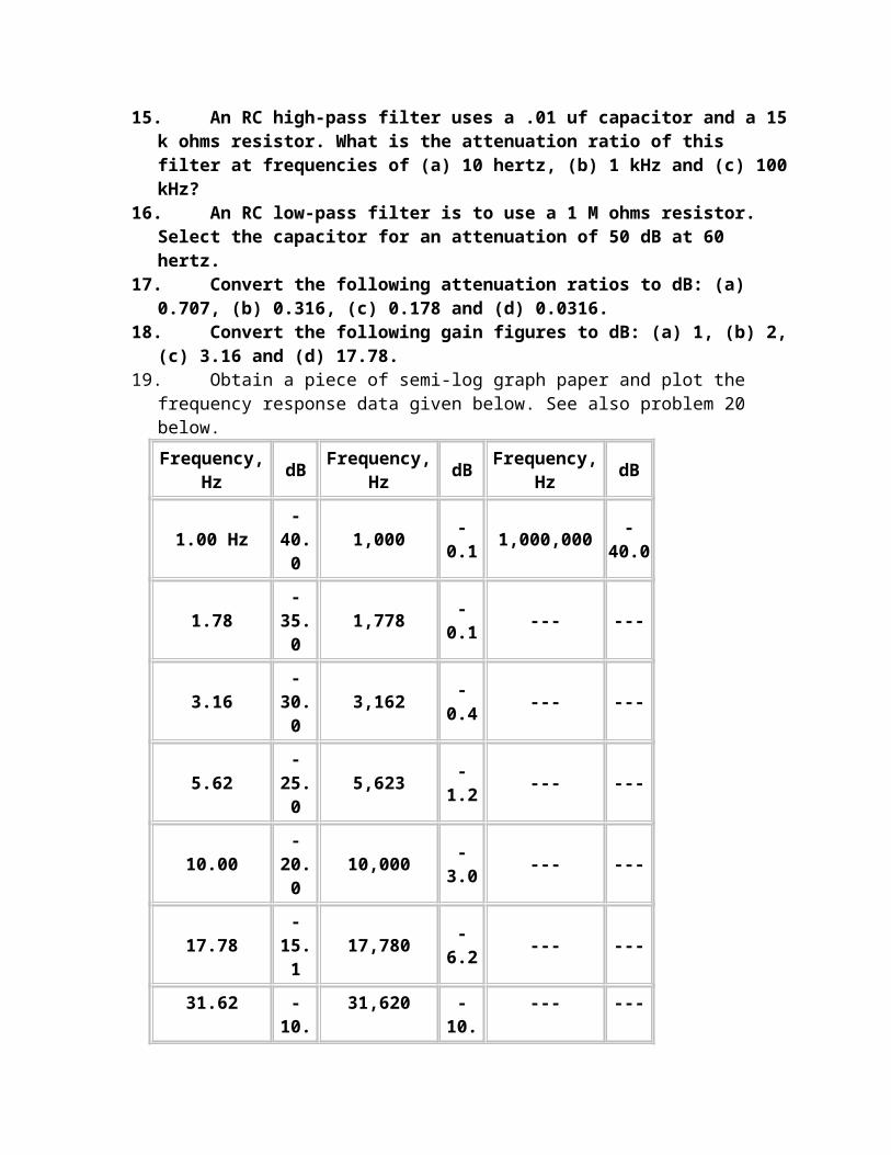
resistor positive. On the second half-cycle the top of the secondary is negative with respect to the center-tap and the bottom is positive with respect to the center-tap. Diode D1 is reversed biased and D2 is forward biased. D1 does not conduct but D2 does. Remember that the bottom end of the transformer secondary is now positive and when D2 conducts, current flows downward through the load resistor, making its top end positive. Current flows through the load on both halves of the input sine wave and both halves appear positive across the load. This process is called full-wave rectification and the circuit is called a full-wave center-tapped rectifier.
The peak output voltage VP of this rectifier is
VP = 1.4 x (VRMS / 2) - Rect Drop. (3.17) where VRMS is the voltage of the entire transformer secondary. Try to understand rather than just memorize. Each half of the transformer winding works alternately so at any given instant only half of the winding is in use. The output voltage is that of only half of the secondary. The factor Rect Drop is the diode drop. The two diodes work alternately and not at the same time. Therefore only one diode drop is subtracted.
Figure 3.9 Full-wave Bridge Rectifier.
For a verbal description click here.
Figure 3.9, above, shows a bridge rectifier circuit. Its output wave looks the same as for Figure 3.8. Because the bridge rectifier uses the whole transformer secondary all of the time, it will deliver twice the voltage at half the current as a full-wave center-tapped rectifier circuit.
When the AC voltage goes positive on the first half-cycle, current flows through D1, down through the load and back to the junction of D3 and D4. The current will not flow through D3. That would be equivalent to a river flowing up a hill. The current flows through D4 to a point of lower electrical potential. On the second half-cycle, current flows through D2, down through the load and back to the junction of D3 and D4. The current will flow through D3 back to the transformer secondary. Regardless of the direction of current in the transformer secondary winding the current always flows downward in the load resistor. The peak output voltage of this rectifier is given by.
VP = 1.4 x VRMS - 2 (Rect Drop) (3.18) where VRMS is the voltage of the entire transformer secondary winding. Try to understand rather than just memorize. The bridge rectifier connects across the entire transformer secondary winding. Each time the current path is traced, it goes through two diodes in series. For this reason you must subtract two diode drops from the output voltage.
Figure 3.10. Two different voltage doubler circuits.
For a verbal description click here.
The circuit of a full-wave voltage doubler is shown in Figure 3.10a above. A voltage doubler circuit will not work without smoothing capacitors. If in the circuit of Figure 3.7 we place a capacitor in parallel with the resistor, the output wave will change. It will now be an almost smooth line at a voltage equal to the peak value of the waveform previously obtained. (Sneak a peak ahead at Figure 3.11. I won't tell if you won't.) If we connect two Figure 3.7 circuits to one transformer (with one diode turned around) we have the circuit of a full-wave voltage doubler as shown in Figure 3.10a. Let us assume that the circuit of Figure 3.10a has been energized for several seconds and both capacitors are charged to their equilibrium voltages. The polarity of charge on the capacitors is as indicated in Figure 3.10a. On the first half-cycle the top of the secondary goes positive with respect to the bottom and current flows through D1 to recharge capacitor C1, which discharged slightly since the last time the top of the transformer went positive. When the top of the secondary goes negative, current flows through D2 replenishing the charge on C2. This circuit consists of two half-wave rectifiers with their outputs connected in series so the output voltage is twice that of one alone.
The charge on C1 is replenished 60 times per second as is the charge on C2. The charges are replenished alternately instead of at the same time; therefore, the total charge is replenished 120 times per second, which qualifies the circuit as a full-wave rectifier.
Figure 3.10b is a variation of the voltage doubler. It has the advantage that one side of both the source and load can be grounded. It has the disadvantage that it is only a half wave rectifier. This circuit is often used in test equipment to obtain the peak to peak value of the incoming wave.
When the input goes negative D1 conducts charging C1 to the peak value of the input with the polarity shown. C1 holds its charge and that voltage is added to the input voltage. When the input goes positive the charge on C1 is added to the peak voltage from the source. This gives a voltage equal to twice the peak or the peak to peak voltage. The wave form at the junction of D1 and C1 is a sine wave which is entirely above the zero axis. D2 rectifies this voltage and charges C2 up to the peak to peak value of the input wave. The charge on C2 is only replenished once for each input cycle or 60 times a second. The peak output voltage of both rectifiers is the same and is given by
VP = 2 (1.4 x VRMS - 0.7). (3.19) where VRMS is the voltage of the entire transformer secondary. Try to understand rather than just memorize. The entire peak secondary voltage is used to charge C1 and then C2. They are in series aiding and the voltage is twice the peak voltage of the secondary. In this circuit as in the bridge there are two diodes effectively in series and so the two diode drops are added together.
Example 3.3
A full-wave center-tapped rectifier circuit (Figure 3.8) employs a transformer which is specified as 9 vCT @ 1 A. What is the peak voltage this rectifier will deliver with semiconductor rectifiers?
Solution:
The full-wave center-tapped circuit uses only half of the secondary at a time; therefore, the output will be the peak of half of the secondary.
VP = (1.4 VRMS / 2) - Rect Drop
VP = 1.4 x 9 / 2 - 0.7 = 5.6 volts.
You could draw 1.4 A from this circuit because the two halves of the secondary are effectively connected in parallel but you are using the peak voltage.
Example 3.4
A full-wave center-tapped rectifier circuit (Figure 3.8) employs a transformer which is specified as 4.50 - 0 - 4.50 vAC @ 1.5 A. What is the peak voltage this rectifier will deliver?
Solution:
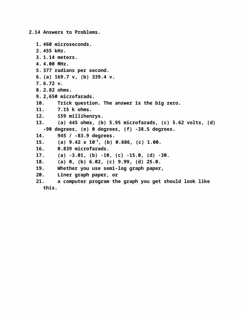
The specification means that the entire secondary voltage is 9 vAC; which is exactly the same as Example 3.3 above. The solution to this problem is exactly the same so there is no need to repeat it.
Example 3.5
A full-wave bridge rectifier (Figure 3.9) employs a transformer which has a 9 volt CT @ 1 A secondary. What is the peak output voltage of this rectifier circuit?
Solution:
The center-tap is not used. The peak output voltage is given by
VP = 1.4 VRMS - 2 x 0.7 = 1.4 x 9 - 1.4 = 11.2 volts.
Remember, these calculations are not all that precise. The available current is 0.7 A maximum.
Example 3.6
A voltage doubler rectifier (Figure 3.10) employs a transformer which has a 9 volt @ 1 A secondary. What is the peak output voltage of this rectifier circuit?
Solution:
The voltage doubler gives twice the peak voltage of the secondary
VP = 2 x (1.4 VRMS - Rect Drop) = 2 x (9 x 1.4 - 0.7) = 23.8 volts.
The original transformer is 9 V at 1 A which is 9 Watts. You can't ask for any more than 9 watts from the rectifier output.
IMax = 9 W / 23.8 V = 0.37 A
This is the maximum current without damage to the transformer.
You have no doubt noticed that the answers in all of the above examples have been rounded off quite a lot. Calculations involving power supplies are among some of the least accurate in electronics. The chief variable in the system is the line voltage provided by the electric utility. In the United States the agreed upon value for the line voltage is 120 volts ± 10 volts. When extra heavy consumer demand drives the utility to the wall, it may even reduce the voltage to 105 volts or less. The writer has personally observed the line voltage at his home and in his office to vary from a low of 114 volts to a high of 128 volts depending on the time of day and season of year. People who design power supplies normally allow large safety margins to prevent malfunctioning of equipment when the line voltage is high or low. With such large safety margins the additional digits of the square root of 2 are just
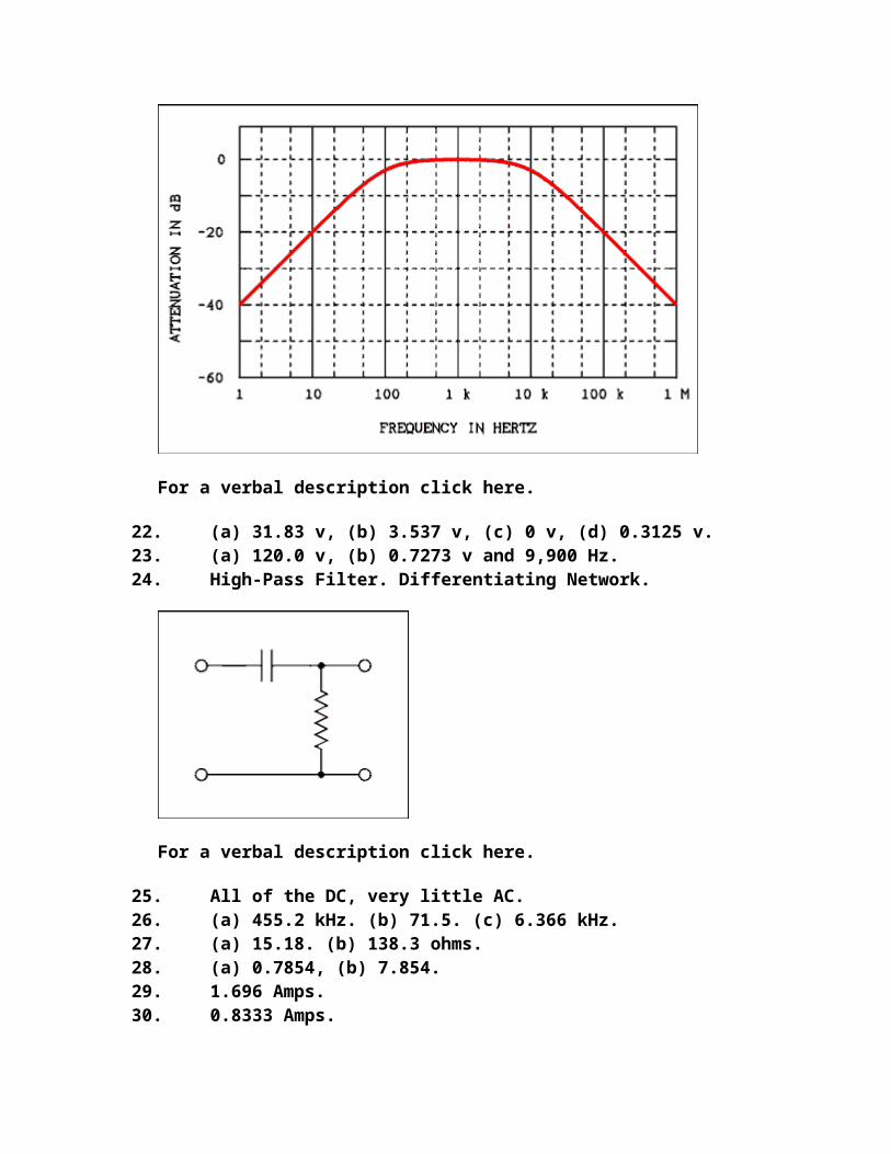
not important. The diode drops should always be taken into account because they lead to a pessimistic design which provides an additional safety margin.
Maximum current.
In the above examples we have sighted a maximum current without fully explaining it. Now we will. You have to think in volt amps. You likely recognize this as watts of power. Lets take the examples above as a starting point. The original transformer was 9 volts at 1 amp. That means 9 watts. If you try to draw 9.1 watts you could get away with it because of some small amount of safety factor built into the design of the transformer. If you try to draw 18 watts you won't have a working transformer for very long.
The available current for the various connections is as follows.
Full-Wave Center-Tapped. IMax = PMax / (1.4 x VRMS / 2)
Full-Wave Bridge Rectifier. IMax = PMax / (1.4 x VRMS)
Voltage Doubler Rectifier. IMax = PMax / [2 (1.4 x VRMS)]
Notice that the diode drops are not subtracted. The power dissipated by the diodes is taken from the transformer and even if it is not available to the load must still be taken into account as power delivered by the transformer.
3.6 Filtering the Rectifier's Output.
Filtering is another name for smoothing. Figure 3.11 shows a full-wave rectifier, one filter capacitor and the output waveform. Power supplies for semiconductor circuits always have additional filtering elements which usually take the form of electronic circuits. Vacuum tube power supplies always have additional filtering elements such as LC (inductor - capacitor) and/or RC (resistor - capacitor) sections. The critical part of most filters is the first capacitor.
Figure 3.11 Rectifier, Filter and wave forms.
For a verbal description click here.
On a positive half-cycle the capacitor will charge through the series combination of half of the transformer secondary winding and diode D1. Because this is a low resistance current path the capacitor will charge quickly. When the positive half cycle falls away, the diode is reverse biased and cannot conduct any current. The capacitor will discharge through the resistor until another positive half cycle comes up to recharge it. The heavy red line shows the voltage across the capacitor and the normal black line shows what the voltage would be without the capacitor.
The lower the resistance of the resistor (the greater the load current), the faster the capacitor will discharge and the lower will be the voltage when the next positive half-cycle comes along. A way to keep the voltage from falling so low between the times when the capacitor is charged is to make the capacitor bigger. Because a full-wave rectifier is being used the charging peaks occur more often than would be the case for a half-wave rectifier. Thus the capacitor will not have as much time to discharge and the voltage will not fall as low as it would with a half-wave circuit. The amount of ripple (variation) in the voltage across the capacitor is given by.
(3.20) Delta V = (I/C) Delta t Now the only question is "how long is delta t?" It is the period of the wave - the charging time. The writer has invested a great deal of work in deriving equations for the ripple voltage (delta V) taking the charging time into account and subsequently many hours in the laboratory attempting to verify the results experimentally. The equations did not predict the voltage any better than plus or minus 20%. These equations did not do any better than setting delta t = a little less than the period of the wave in equation 3.19. The conclusion is to set delta t = 8 ms approximately (1/120) for a full-wave rectifier or 16 ms approximately (1/60) for a half-wave rectifier. These numbers would be different for someone living outside of North America. Solving equation 3.19 for C gives
(3.21.1) C = (I Delta t)/(Delta V) One more definition is necessary. That is the Valley voltage VV. The valley voltage is exactly what you would think it is, the lowest voltage of the ripple. It may seem a little tricky in a negative power supply so we define the valley voltage as that part of the ripple wave which comes closest to zero. The peak voltage of the ripple, VP, is that part of the wave which is farthest from zero.
VV = VP (3.21.2) - Delta V
Example 3.7
A 25.2 vCT @ 1 A transformer is being used in a full-wave center-tapped power supply which is to deliver 150 mA to the heater of a 12AX7 (DC heater supply to reduce hum). (a) Calculate the correct capacitor to give a ripple of 1.2 volts or less, (b) calculate the DC voltage at the capacitor, (c) the value of the resistor required to apply 12.6 volts to the heater of the tube, and (d) the wattage of the resistor.
Solution:
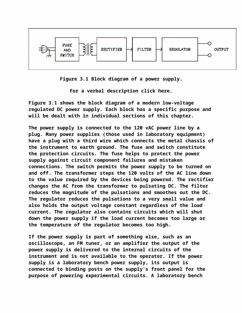
(a) Using equation 3.21.1 for C gives
C = (0.15 A x 8 ms)/(1.2 V) = 1000 microfarads.
(b) The DC output voltage is
VDC = 1.4 x 25.2 / 2 - 0.7 = 16.94 volts.
That's the peak voltage. The DC is the average voltage which is half of the ripple less than the peak voltage or 16.94 - 1.2 / 2 = 16.34 volts; let's call it 16.3 volts.
(c) The resistor is given by ohm's law as follows.
R = (16.3 - 12.6) / .15 amps = 24.7 ohms.
Use a 24 ohm resistor.
(d) The power dissipated by the resistor is given by
P = I squared R = .15 squared x 24 = .54 watts
Use a 1 watt resistor. Most designers would likely connect another 1000 microfarad capacitor from the other end of the 24 ohm resistor to common as shown in the figure below.
Figure 3.12.1 DC Heater Supply for 12AX7.
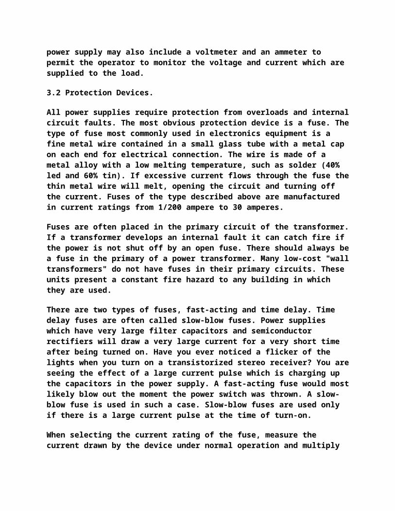
For a verbal description click here.
Example 3.8.1
A full-wave bridge rectifier is to be used with a transformer which is rated as 28 vCT @ 2 A. The capacitor is 2200 uf and the load current is 1.3 A. What is the ripple voltage?
Solution:
Using equation 3.19 we have,
Delta V = (I/C) Delta t = (1.3 A / 2200 rf) x 8 ms = 4.7 V.
As compared to physical reality, this is a pessimistic prediction.
Example 3.8.2
A full-wave bridge rectifier is to be used with a transformer which is rated as 280 vCT @ 250 mA. The capacitor is 22 mu f and the load current is 85 mA. What is the ripple voltage?
Solution:
Using equation 3.19 we have
Delta V = (I/C) Delta t = (85 mA / 22 mu f) x 8 ms = 30.9 V
As compared to physical reality, this is a pessimistic prediction.
Additional Filtering LC section.
Electronic voltage regulators are not often used in vacuum tube circuits. When lower ripple is desired from a power supply than can be obtained from a single capacitor, additional filtering elements are added to the filter. For example an LC section may be added to the single capacitor filter to obtain the circuit shown below.
Figure 3.12.2 Full-wave rectifier and C-L-C filter.
For a verbal description click here.
The inductor has a low resistance to DC but a much higher reactance to the AC ripple. Because it is a series element it drops very little DC while dropping a large amount (most of it in fact) of the AC. The second capacitor presents an open circuit to the DC but a low reactance to the AC ripple. It, together with the inductor, forms a voltage divider which reduces the ripple to a very low level. If X<SUBL< sub> is much greater than XC the ripple across C2 is given by
VC2 = VC1 (XC2) / (XL (3.22) )
where
XL (3.23) = 2 pi f L and
XC2 = 1 / (2 pi f C2 ) (3.24) Substituting equations 3.23 and 3.24 into equation 3.22 gives.
VC2 = (VC1) / (4 pi squared f squared L C2 (3.25) ) The DC voltage drop across the inductor (filter choke) is usually small enough to be neglected.
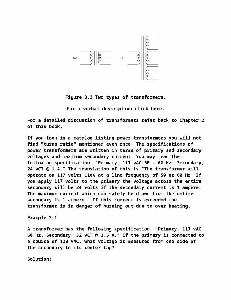
Additional Filtering RC section.
If an RC section is added to the single capacitor filter we have a circuit like that shown below.
Figure 3.12.3 full wave rectifier and C-R-C filter.
For a verbal description click here.
The resistor has the same resistance to DC and AC. Because it is a series element it drops a moderate amount of DC while dropping a large amount (most of it in fact) of the AC. The reason the resistor drops more AC than DC is because the second capacitor presents an open circuit to the DC but a low reactance, almost a short, to the AC ripple. It, together with the resistor, forms a voltage divider which reduces the ripple to a very low level. If R is much greater than XC2 the ripple across 2 is given by
VC2 = VC1 (XC (3.26) ) / (R) where
XC2 = 1 / (2 pi f C2 ) (3.27) Substituting equation 3.27 into equation 3.26 gives.
VC2 = (VC1) / (2 pi f R C2 (3.28) ) The DC voltage appearing across C2 is given by
VDC-C2 = VDC-C1 - ILoad (3.29) R
Where ILoad is the sum of all DC load currents taken off from C2, C3, C4, Etcetera. Additional series R and parallel C sections may be, and often are, added on the end of the circuits of 3.12.2 or 3.12.3. Each added capacitor is numbered C3, C4, etc.
Example 3.9
A filter like that of Figure 3.12.2 has two 22 microfarad capacitors and an 8 Henry filter choke. The ripple voltage across C1 is 31 volts (Example 3.8.2). What is the ripple voltage across C2?
Solution
Using Equation 3.25 gives.
VC2 = (VC1) / (4 pi squared f squared L C2)
VC2 = 31 vAC / (4 pi squared x 120 squared x 8 henrys x 22 mu f = 0.31 vAC.
Example 3.10
A DC power supply like that of Figure 3.13 uses a transformer with a high voltage winding having a rating of 325 - 0 - 325 volts at 100 mA. (This current rating is for a capacitor input filter so the factor of 1.4 has already been accounted for.) It uses a 5Y3 rectifier tube and an RC filter with two 40 mu f capacitors and a 1 k ohm resistor. The DC load taken off at C1 is 80 mA and the load taken off at C2 is 15 mA. What are (a) the ripple across C1, (b) the ripple across C2, (c) the DC voltage across C1, and (d) the DC voltage across C2?
Solution
(a) The ripple across C1 is given by equation 3.19 which is.
Delta V = (I/C) Delta t
We must use the sum of the currents for I in this equation which is 95 mA.
Delta V = (95 mA/40 mu f) 8.3 ms = 19.7 volts.
Let's call it 20 volts.
(b) The ripple across C2 is given by equation 3.28.
VC2 = (VC1) / (2 π f R C2)
VC2 = 20 / (2 π 120 1000 40 mu f) = 0.66 volts.
(c) Using equation 3.17 gives
VDC = 1.4 VRMS / 2 - Rect Drop = 1.4 x 650 / 2 - 125 = 330 volts
The graphs in the tube manual for the 5Y3 give an output voltage of 330 volts for a load of 95 mA and a voltage on each plate of 325 volts.
(d) The voltage across C2 is given by equation 3.29 as
VDC-C2 = VDC-C1 - ILoad R = 330 V - 15 mA x 1000 Ω = 315 VDC
3.7 Zener Diode and Gas discharge Voltage Regulators.
Preliminary, Classes of Voltage Regulators.
There are two classes of voltage regulators, series and shunt. The way a voltage regulator works is to place a variable resistance element either, in series with, or in shunt with the voltage to be regulated. Figure 3.12.1 shows a shunt regulator in (a) and a series regulator in (b).
Figure 3.12.1 Shunt and Series Regulators.
For a verbal description click here.
The Shunt Regulator.
Circuit (a) is a shunt regulator. The variable resistance element works to keep the voltage across the output terminals constant. It's resistance changes as needed to accomplish this. The load, which is connected across the output terminals, must operate at a voltage lower than the lowest output voltage of the rectifier and filter.
Let us say that the regulator is operating normally. Then the voltage of the rectifier/filter increases. For the load voltage to remain constant there must be an increased voltage drop across the fixed resistor. Ohm's law tells us that the current through the resistor must
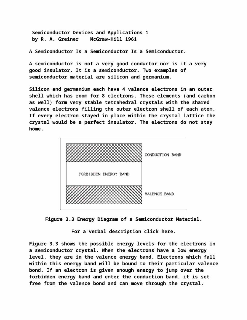
increase. The regulator element, inside the red box, will change its resistance to draw more current and the output voltage remains constant.
Now suppose the load current decreases a little. This would cause a decreased drop across the fixed resistor but the regulator compensates by decreasing its resistance to take more current. If the load current goes all the way to zero the regulator will take it all.
If the load current increases the regulator current will decrease to keep the voltage across the output terminals constant. However if the load current increases to the point where the regulator current goes to zero that's as far is it can go. After all the regulator is a variable resistor so it can't generate additional voltage. If the load current keeps increasing after the regulator current has gone to zero the voltage will fall below the regulated value because the regulator is powerless to prevent it from falling below the set voltage. This is the chief disadvantage of a shunt regulator. The regulator will also lose control if the rectifier/filter voltage falls so low that the regulator current goes to zero.
A regulator of this type wastes a lot of power. The current through the regulator must be set above the maximum current that the load will ever take. If this happens for only a small percent of the time and operates at say 1/10 of that value most of the time the shunt regulator will always draw the highest current from the rectifier/filter. If the rectifier/filter were replaced by a battery, it would be discharged very quickly by the large amount of current demanded by the shunt regulator.
The Series Regulator.
In Figure 3.12.1 (b) above the series regulator is connected in series with the load. This type will hold the voltage across the output terminals constant. It does this by comparing the output voltage to a reference voltage and using vacuum tube, transistor, or operational amplifiers (op amps) to amplify the difference and control the pass element. The actual pass element may be a transistor, or vacuum tube, but we don't know about such things yet so we will just think of it as a variable resistor that uses some form of magic to sense the voltage across the output terminals and adjust itself.
Notice that there is no extra resistor in the circuit. Whatever current the load draws, that much current will flow through the regulator, and the same amount will be drawn from the rectifier/filter. The voltage from the rectifier/filter can change up or down and the series regulator element will adjust it's resistance to compensate. The load current can change up or down, even to zero, and the series pass element will adjust to compensate. Series regulators are more efficient than shunt regulators because in the absents of load current they draw very little current from the source. The amplifiers that make it work need a little current but it isn't very much. In general a series regulator can operate with its input and output voltages closer together than for a shunt regulator. That makes them more efficient and a better choice for regulating the voltage in battery operated equipment.
Shunt Zener Diode Regulator.
If a specially manufactured P-N junction diode is reversed biased it presents a constant voltage characteristic. This constant voltage characteristic is perfect for a shunt voltage regulator.
If the doping level (amount of impurity) is increased in a P-N junction the reverse breakdown * voltage will be decreased. When a P-N junction breaks down in the reverse direction, the voltage is held constant (regulated) even though the current may vary over a large range. The typical characteristic of a P-N junction is shown in Figure 3.13. The portion in the first quadrant is the same as any other P-N junction diode. The portion in the third quadrant is the reverse breakdown * characteristic. As the voltage increases in the negative direction, nothing happens until the voltage reaches the constant voltage breakdown point. When this point is reached, the current goes up very rapidly and the voltage will not increase any further. If an attempt is made to force the voltage higher the diode will overheat very quickly and burn out.
* The term "breakdown" does not mean a malfunction as it does to an auto mechanic. In semiconductor talk "breakdown" means the beginning of conduction of current. A diode which has broken down does not have to be replaced; it is just beginning to go to work.
Figure 3.13 I-V Curve of a P-N Junction Diode.
For a verbal description click here.
There are two mechanisms of reverse breakdown, Zener and avalanche. In Zener breakdown (named for its discoverer Clarence Zener) the electric field intensity in the depletion region becomes so great as to promote electrons from the valence energy band to the conduction energy band. The electrons on the P side move toward the junction and contribute to conduction. Electrons which are freed on the N side cause holes to be created which move toward the junction and also contribute to conduction. The threshold at which electrons begin to be promoted is very sharp and the so- called Zener breakdown voltage is very constant. Zener breakdown takes place up to about 6.2 volts.
If the doping has not been increased to the level where the reverse breakdown is below 6.2 volts, the mechanism is avalanche breakdown. When the electric field becomes intense enough to promote electrons to the conduction band they are accelerated by the field. These newly freed electrons collide with other valance electrons and promote them to the conduction band which in turn collide with other valence electrons promoting them to the
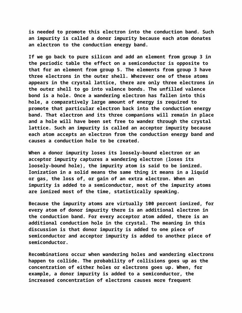
conduction band et cetera, et cetera. Avalanche breakdown occurs if the breakdown voltage is greater than about 6.2 volts.
As you might expect the transition from Zener breakdown to avalanche breakdown is not a sudden one but a gradual one. That has interesting consequences because of the temperature coefficients of the two processes. Avalanche breakdown has a positive temperature coefficient and Zener breakdown has a negative temperature coefficient. At the voltage where the two effects play an equal role in reverse breakdown the temperature coefficient is exactly zero. This is at a voltage of 6.1 and some more decimal places.
It used to be literally true that diode manufacturers would make a batch of diodes and then test them to see what they had made. That is no longer completely true but when Zener diodes are being manufactured in the neighborhood of 6 volts, they are carefully tested. The ones which fall exactly on the magic zero temperature coefficient voltage are pulled out and sold for ten dollars a piece as reference diodes. The ones which don't pass this test are sold as 6.2 volt 5% units for seventy five cents or as 5.6 volt 10% units for forty cents. The manufacturing cost is a fraction of a cent per diode. The cost is in the testing. Even though the mechanism may be avalanche breakdown, the diodes are called Zener diodes.
Uses for the Zener Diode.
Zener diodes are sometimes used to set an upper limit to a voltage. Because it draws essentially zero current before breakdown it works well in this application. Suppose an input circuit of an amplifier is meant to operate from zero to 10 volts but would be damaged if the voltage exceeded 12 volts. A 12 volt zener diode can be placed across the input and will have no effect on voltage within the intended range of the amplifier but will conduct and prevent the voltage from going higher than the damaging value of 12 volts.
Zener diodes are also used as voltage regulators. They were formerly used to regulate voltage in both low and high power circuits. Units were available in power ratings from 1 to 50 watts. In modern electronics the Zener diode is used to provide voltage references to high power regulators. The Zener diode is a low power unit and a power transistor takes care of any heavy work. Power transistors cost much less than power Zener diodes. Zeners are now available as 0.4, 1, and 5 watt units.
A typical circuit for a Zener diode voltage regulator is shown in Figure 3.14. The input is an unregulated power supply consisting of a circuit such as Figure 3.11 without the resistor. The load current which is drawn from the output can range from a few nanoamps to several tens of milliamps.
How a voltage regulator works and what it does.
A voltage regulator has to hold the voltage constant as the voltage of the input varies and as the load current changes. The output voltage of a rectifier and filter capacitor is not constant. As mentioned earlier the line voltage can vary all over the place and then there is that ripple which is always present. Another application is in battery operated equipment.
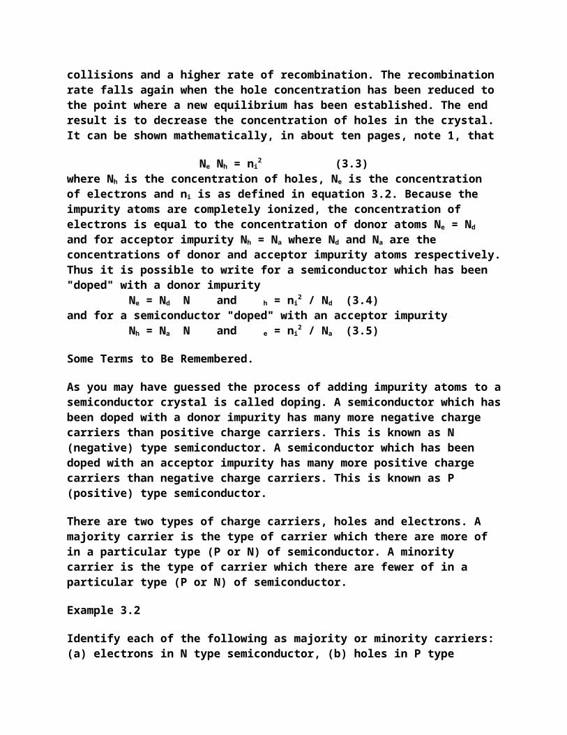
In many cases the designer of such equipment wants the voltage applied to the circuits to remain constant as the batteries run down. The battery voltage is set higher than the circuit needs and the regulator holds it constant until the voltage gets near the operating voltage. Special circuits usually warn the operator and/or turn off the equipment when the battery is so run down as to no longer operate the device.
Changing load current is another difficulty. We have used resistors to indicate the load on a power supply. The real load on a power supply is a transistor circuit and/or a small motor or two. The current drawn by a transistor circuit may change depending on what the circuit is and what it is doing at the moment. The current drawn by a motor changes as its mechanical load changes. So a regulator may have a lot to do.
A regulator can't increase the voltage applied to it. All it can do is reduce it. It regulates the voltage by reducing it by the amount required to hold it at some preset value. The difference between the regulator input and the output is called the regulator drop. Each type of regulator has it's minimum regulator drop. If the input voltage falls so low as to make the regulator drop less than the minimum the regulator will lose control and the output voltage will fall.
For example, a 12 volt regulator IC has a minimum drop of 2 volts. That means that the input voltage must be 14 volts or higher. It regulates just fine for input voltages anywhere from 14 to 40 volts. But if the input voltage falls to 13 volts the output voltage will fall to 11 volts and it will no longer be regulated. It will just be 2 volts less than the input, ripple and all. If the ripple valley falls below the minimum required the output voltage will acquire ripple as shown in the graph below.
Figure 3.14 Input and output waves of a voltage regulator.
For a verbal description click here.
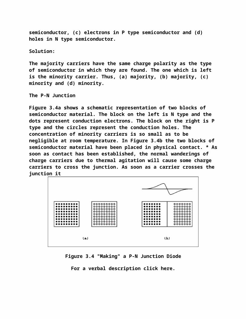
The upper wave is the output of a full wave rectifier with a capacitor filter. The lower wave is the output voltage of a voltage regulator. In (a) the input voltage is high enough that the regulator is able to do its job properly. In part (b) increased load current has pulled the ripple valley down so it is below the minimum required to maintain regulation. Note that the peak voltage is the same in both cases. This is the way ripple responds to increased load current.
A measurement with a DC voltmeter is likely to indicate that the input voltage is high enough but the ripple valley is too low. Only an oscilloscope measurement will reveal this defect. I have taught the senior projects course in the electrical engineering department for several years and I have found this to be one of the most common mistakes in circuit design.
The Zener Diode Voltage Regulator.
There is one thing about the following calculations you may find peculiar. The maximum allowable current in a zener diode is that which gives 1/4 of the rated power. The specified power rating for almost all semiconductor devices is given for the temperature of the silicon crystal to be held to 25 degrees C. This is stated in the literature as the junction temperature. About the only way to achieve this with a zener diode would be to operate it amerced in a stirred and cooled oil bath.
The power can be increased to about 1/2 of the specified power by mounting the diode through a hole in a heat sink and coating it with heat sinking compound. The hole should be sized so the diode is a tight fit and the sink should be as thick as the diode is long. When the diode is operated in open air the maximum power is 1/4 of the specified power. Operation at higher power will cause the diode to overheat and fail.
Figure 3.15 Zener Diode Voltage Regulator Circuit.
For a verbal description click here.
To design a zener diode circuit you only need to specify the zener diode, voltage, and power, and the resistor RA, resistance, and wattage rating. After the value of RA is fixed, the minimum regulation voltage must be determined. Remember that the Zener diode holds its voltage constant. If the input voltage changes, the voltage across RA must change.
Remember Kirchhoff's law? VIN = VRA + VZ where VIN is the input voltage, VRA is the voltage across RA and VZ is the voltage across the Zener diode. If VZ is constant, VIN and VRA will rise and fall together. The current through RA is also proportional to the voltage across RA. Let us assume that there is a load of 1 mA on the output of the regulator. That means that of the current through RA, 1 mA will flow through the load and the rest will flow through the Zener diode because IRA = IL + IZ. The power in the Zener diode is PZ = IZ VZ. Normal practice is to set the current through the Zener diode to such a value as to dissipate 25% of the diode's rated power. Regulation can be maintained as long as the current through the Zener diode is greater than zero. If the current tries to reverse, it cannot and regulation will be lost. The zener diode can't become a battery and hold the voltage up if the input falls below the minimum input voltage. Solving this problem is nothing more than the repeated application of Ohm's and Kirchhoff's laws and should not require any memorization.
The rules for design are as follows.
1. Calculate the Zener diode current for 25% of rated power. 2. Add any load current to this Zener current. This is the current through RA. 3. Subtract the Zener voltage from the average expected input voltage. 4. Use results of 2 and 3 in Ohm's law to calculate the resistance of RA. 5. Calculate the minimum input voltage for regulation to be maintained. This value
must be below the ripple valley voltage of the power supply. 6. Calculate the power dissipation of the resistor based on the average ripple voltage. * 7. Calculate the maximum power dissipated by the zener diode based on minimum
load current, often zero, and average input ripple.
* because the power is proportional to the square of the voltage, using the average voltage is not quite correct. However, for realistic values of ripple the error is so small as to be unimportant.
Example 3.10.
An unregulated power supply delivers a ripple peak of 21 volts and a ripple valley of 19 volts. The Zener diode regulator circuit is to deliver 12 volts at 2 mA and will use a 12 volt 400 milliwatt Zener diode. What is (a) the value of RA, (b) the average power dissipated in RA and (c) the minimum input voltage to maintain regulation?
Solution:
The ripple waveform may be approximated as a series of straight lines and the average is simply (VP + VV) / 2 or (21 + 19) / 2 = 20 v. 25% of 400 mW is 100 mW; therefore, IZ = 100 mW / 12 v = 8.3 mA. (a) The value of RA is
RA = (VIN - VZ) / (IZ + IL)
RA = (20 v - 12 v) / 8.3 mA + 2 mA) = 780 ohms.
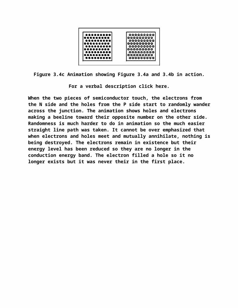
(b) Power in RA is P = (20 v - 12 v)2 / 780 ohms = 0.082 W
(c) Let IZ = 0.
VIN = VZ + IL RA = 12 v + 2 mA x 780 ohms = 13.6 volts.
This is much less than the ripple valley voltage of 19 volts, so the circuit will work.
The only resistors which come in what ever value you need are .05% precision resistors and these are very, very expensive. In common laboratory work we must use what the manufacturers of resistors supply us. The result of (a) in the above example was 780 ohms. In standard 5% resistor values the two closest values are 750 and 820 ohms. In this case you would tend to choose 750 ohms because it is the closest one and you would be doing the right thing. In Zener diode circuits you should always move down to the next lower value. The calculations of parts (b) and (c) should be based on the actual resistor used rather than the calculated value.
The writer considers the memorization of the table of standard values to be a waste of time and effort. This is information which can always be looked up if and when it is needed. A table of standard values is given in the appendix for those who need to look them up.
Example 3.11.
An unregulated power supply delivers a ripple peak of 39 volts and a ripple valley of 25 volts. The Zener diode regulator circuit is to deliver 16 volts at 1 mA and will use a 16 volt 1 watt Zener diode. What is (a) the value of RA, (b) the average power dissipated in RA and (c) the minimum input voltage to maintain regulation?
Solution:
The average input voltage is (39 + 25) / 2 = 32 volts. The Zener diode current is IZ = 0.25 x 1 W / 16 v = 15.6 mA. (a) RA = (32 - 16) / (15.6 + 1) = 964 ohms. The next lowest standard value is 910 ohms and that is what we will use. (b) The power is (32v - 16v)2 / 910 ohms = 0.28 watts. It is best to use a 1/2 watt resistor here. (c) The minimum input voltage is 16 v + 1 mA x 910 ohms = 16.91 volts. The circuit will work.
Zener diode voltage regulators are occasionally used to regulate the voltage for low current circuits when a design goal is to keep it simple. Because it is a shunt regulator it wastes too much power to be used in a battery operated device.
Zener diodes are most often used in conjunction with other circuits such as op amps and power transistors. We will return to these circuits later after we have studied these devices.
If You Need a High Power Zener.
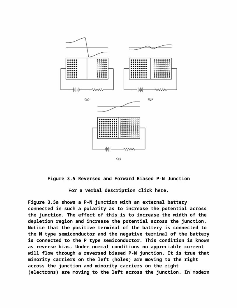
Although zener diodes are no longer available in powers above 5 watts, (1.25 watts in practice), they can be obtained in voltages up to 100 volts. If you need to regulate a voltage at high current and/or high voltage, relatively speaking, you can use a transistor to effectively amplify the power of a zener diode.
Figure 3.15.1 Amplified Zener Diode Voltage Regulator Circuit.
For a verbal description click here.
As the input voltage increases the transistor remains an open circuit until it experiences base current. There is no base current until the zener diode begins to conduct so the whole thing is an open circuit until the zener voltage + 0.6 volts is reached. When the zener does begin to conduct the transistor also begins to conduct but the collector current is typically 100 times as large as the current through the zener diode and into the base. If you need a high power shunt regulator This is the circuit for you. Remember the turn on voltage is 0.6 volts higher than the zener voltage.
Gas Discharge Regulator Tubes.
Prior to the invention of the zener diode the only regulating devices were gas discharge regulator tubes, commonly known as voltage regulator or VR tubes. These are cold cathode diode tubes filled with one of the inert gases. The pressure is low, about 1/100 of an atmosphere. They come in four voltages, 75, 90, 105, and 150 volts. The only gas I can identify with a specific voltage is neon with the 75 volt tube.
The workhorse set is the octal series, 0A3, 0B3, 0C3, and 0D3. The 0A3 is the 75 volt tube and the 0D3 is the 150 volt regulator. The current range is 5 to 40 mA for all tubes. There is a 7 pin miniature series 0A2, 0B2, and 0C2. Their voltages are 150, 105, and 75 respectively. Their maximum current is 30 mA.
The design procedure is almost the same as for the zener diode, with one exception. The glow discharge in the tubes require a higher voltage than the operating value to get the ionization started. This value is different for each tube and must be looked up in a tube manual. The initial voltage of the power supply must be above this starting value and the
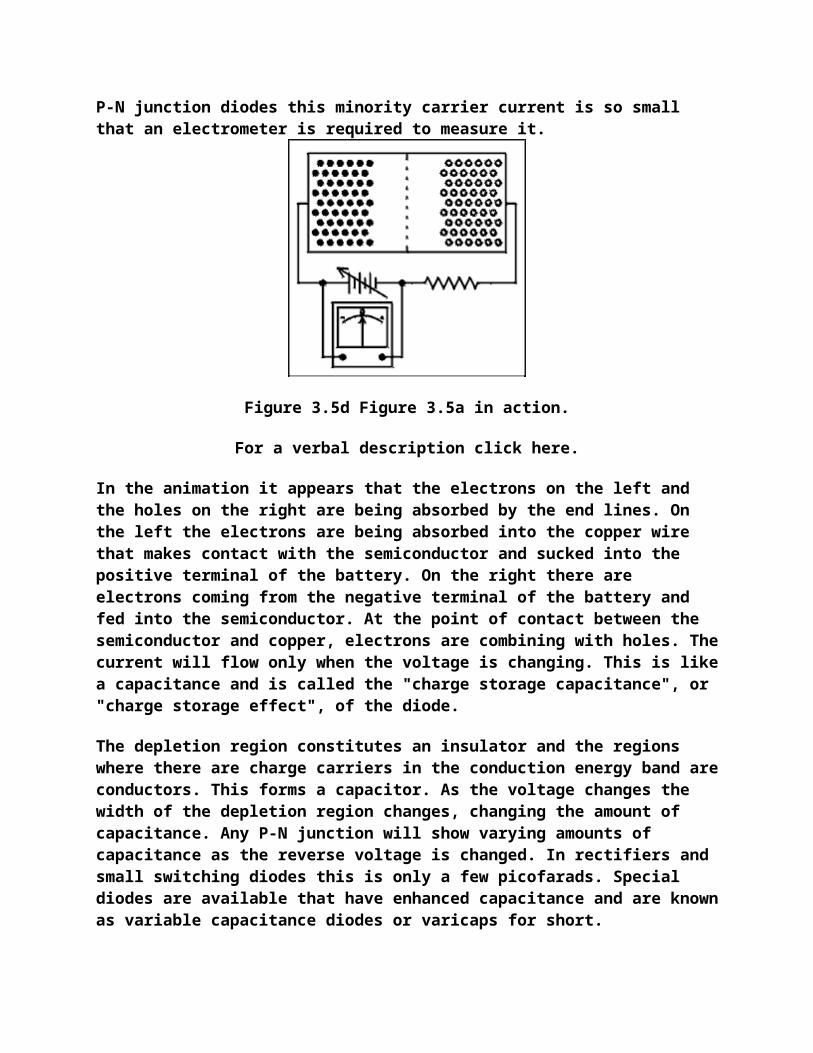
starting current of the load must be zero or very small. If the load is resistive, the voltage of the power supply must be large enough to place the starting voltage on the tube even with the load drawing current. The schematic symbol of a VR tube can be seen in a diagram at the end of this chapter.
3.8 Integrated Circuit Voltage Regulators.
The design and construction of power supplies using series regulators has been made extremely simple by the introduction of the integrated circuit voltage regulator. The IC VR could not possibly be any simpler. It has three terminals: an input, an output and a ground (common). It is often called a three terminal regulator. The acronym "TTR" has never been seen or heard by the writer. The schematic symbol for the IC VR is just a rectangle with 3 lines (wires) connecting to it.
These regulators regulate very well against changes in load current and changes in input voltage. Most of the ripple voltage which is present in the output of the unregulated power supply is regulated out by the IC VR. The IC contains a current sensor and the voltage will be shut down if the load tries to draw too much current. The IC also contains a temperature sensor and, if the IC gets too hot, the voltage will be shut down. When the power is turned off the IC will cool down and the power will be turned back on again. The observable results of an IC VR which is getting too hot is that the voltage will be turned off and on periodically.
One undesirable thing that these little wonders do rather well is to oscillate at a frequency of approximately 1 Megahertz. This oscillation can cause lots of trouble and headaches for research lab workers (graduate students). The way to prevent these oscillations is to connect a 0.1 uf capacitor on each side of the regulator, one from input to ground and the other from output to ground. These capacitors must be physically close to the regulator or they will not do any good. A regulator which does not have these capacitors will, not may, but WILL, oscillate. In addition to these capacitors, the unregulated power supply must have its filter capacitor and a capacitor in the neighborhood of 25 uf connected across the output of the voltage regulator. Figure 3.16 is the circuit of a typical 5 volt 1 amp power supply.
Figure 3.16 Complete 5 Volt 1 Amp Power Supply.
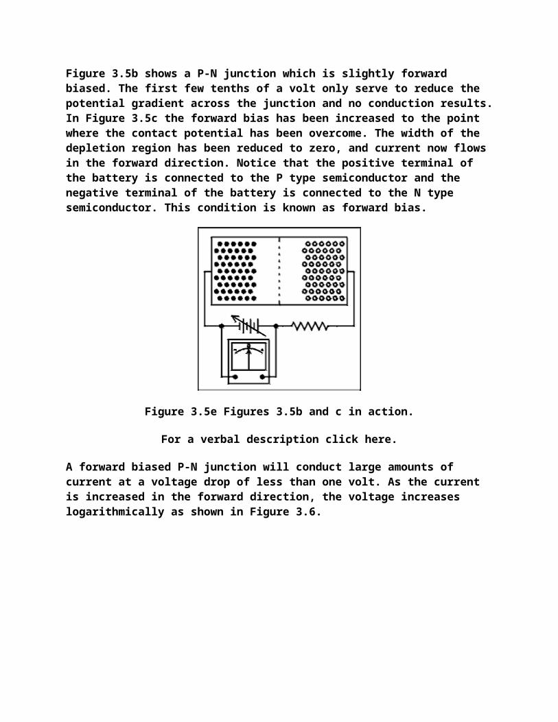
For a verbal description click here.
These IC VRs come in a wide variety of shapes and sizes but by far the most popular are the LM78XX and LM79XX regulator series. These are supplied in a TO220 (see appendix B) package which must be attached to a heat sink if it is to deliver any more than 100 mA. The LM78XX are positive regulators and the LM79XX are for regulating negative voltage power supplies. The "XX" gives the output voltage of the regulator. For example an LM7805 is a +5 volt unit, an LM7812 is a +12 and an LM7915 is a -15 volt unit. All of these units will accept input voltages of VO + 2 to 40 volts for a positive regulator and VO - 2 to -40 volts for a negative regulator. They will deliver a maximum of 1 ampere and are current limited at about 1.5 amperes.
There is another series of regulators which are very useful in low power circuits. They are the LM78LXX and LM79LXX series. These regulators are supplied in a TO92 package and have a maximum current rating of 100 mA. These units usually do not need a heat sink. The small package makes it possible to construct a very small low-power power supply.
Adjustable Voltage Regulators.
If you need a voltage in between the voltages of the fixed regulators, or you want to build a variable voltage power supply, there is another set of voltage regulators which have adjustable output voltages. The positive regulator is an LM317 and the negative regulator is an LM337. A possible disadvantage of these regulators is that their voltage will not go all the way to zero. Here is the circuit using an LM317.
Figure 3.17 Circuit of an adjustable voltage regulator.
For a verbal description click here.
This circuit works because the voltage between the O and A terminals is fixed at 1.2 volts, and current flowing out of the A terminal is very small. The fixed output voltage causes the current through R1 to be constant. The small current in the A terminal causes the current
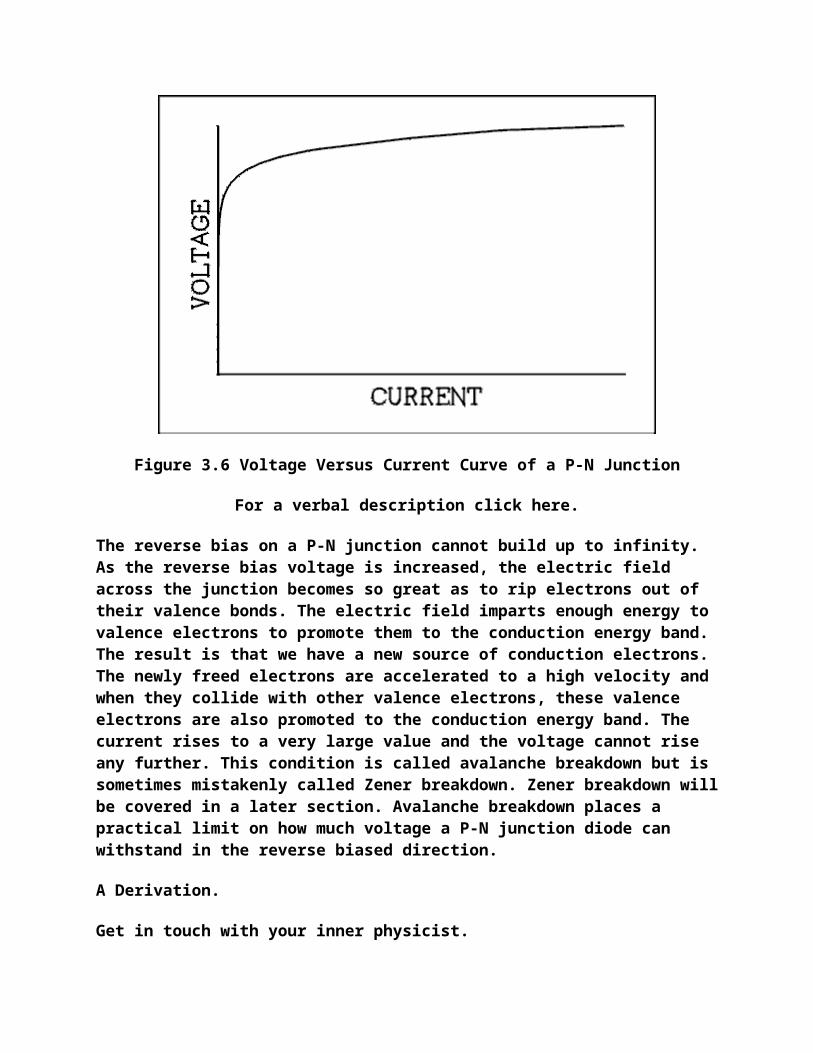
in R2 to be essentially equal to the current in R1. This means that the drop across R2 will be constant and set by the values of R1 and R2.
Example 3.12.
If R1 is 100 ohms and R2 is 1100 ohms, what is the output voltage of the circuit?
Solution:
The voltage between the O and A terminals is 1.2 volts so the current in R1 is,
I = 1.2 / 100 = 12.0 mA.
The current in R2 is also 12 mA so the voltage across R2 is,
V = 12.0 mA x 1100 ohms = 13.2 volts.
This is not the output voltage, it is the voltage between common and the A terminal. The voltage between the o terminal and common is the sum of the voltage between common and the A terminal and the voltage between the A and O terminals or,
13.2 + 1.2 = 14.4 volts.
A triple output 1.2 to 20, -1.2 to -20, and fixed 5 volt, power supply is shown in Figure 3.18. The diodes across the output are to prevent either supply from being pulled to the opposite sign by the other power supply. If this happens, the supply will latch at -0.7 volts and will not come up to its normal voltage.
Figure 3.18 Triple Voltage Power Supply.
For a verbal description click here.
Vacuum Tube Voltage Regulator.
Some vacuum tube circuits require regulated voltage. These include such things as the amplifiers in Vacuum Tube Volt Meters (VTVM), The screen grids of high power amplifiers, and oscillators in communications receivers and transmitters. These applications are not usually high current. It is not necessary to regulate the plate voltage of a power amplifier. If the voltage needed does not fall on one of the 4 VR tube values an electronic circuit must be used. Here is a simple regulator circuit.
Figure 3.19 Vacuum Tube Voltage Regulator Circuit.
For a verbal description click here.
The 0A3 is a VR tube as described above. If the device containing the regulator were to be operated with the VR tube unplugged some circuit components could be damaged. The connection between pins 3 and 7 of the tube is a jumper. If the tube is removed from its socket there will not be any output from the circuit because the negative lead is open. Removing a positive voltage from something will usually result in less current rather than more.
This circuit will not go to zero voltage. One that will, needs a negative voltage supply and can get more complicated. This circuit is as simple as it can get and still be a true closed loop* regulator.
* A closed loop regulator is one in which the output voltage is sensed, compared to a reference voltage, and if the output voltage changes it is instantly corrected to the set voltage.
A common feature of regulators is that the heater of the pass tube, the 6AQ5 in this circuit, is operated from a separate filament transformer. The maximum heater to cathode voltage for most tubes is 200 volts so a regulator capable of output voltage higher than this must have such a transformer. One side of the heater is tied electrically to the cathode so the voltage difference is no more than the peak of the 6.3 volt heater supply voltage.
3.9 Problems.
1. The unregulated portion of a power supply is delivering 18 volts at a current of 1 ampere. What size (current rating) fuse should be used in the primary of the transformer?
2. A power transformer has the ratings 34 - 0 - 34 v @ 3 amps. If this transformer is used with a full-wave center-tapped rectifier circuit, Figure 3.8, what is the peak output voltage VP? Take diode drops into account.
3. A power transformer has the ratings 36 vCT @ 2 amps. If this transformer is used with a full-wave center-tapped rectifier circuit, Figure 3.8, what is the peak output voltage VP? Take diode drops into account.
4. A power transformer has the ratings 21 vAC @ 5 amps. If this transformer is used with a full-wave bridge rectifier circuit, Figure 3.9, what is the peak output voltage VP? Take diode drops into account.
5. A full-wave voltage doubler circuit (Figure 3.10) is attached to a transformer whose secondary is rated at 120 vAC @ 10 amperes. (This is an isolation transformer.) What is the peak output of this circuit? Take diode drops into account.
6. A power transformer is rated as 40 - 0 - 40 vAC @ 1.2 amps. The transformer is equipped with a full-wave center-tapped rectifier using silicon diodes and a filter capacitor of 7,000 microfarads. What is the ripple valley voltage of this circuit if the load current is 0.8 ampere? Apply all corrections.
7. A power transformer is rated as 20 vAC @ 7 amps. The transformer is equipped with a full-wave bridge rectifier using silicon diodes and a filter capacitor of 20,000 microfarads. What is the ripple valley voltage of this circuit if the load current is 5 amperes? Apply all corrections.
8. Using the transformer and rectifier from problem 6, calculate the value of the filter capacitor to give a ripple valley voltage of 45 volts if the load current is 0.8 amps.
9. Using the transformer and rectifier from problem 7, calculate the value of the filter capacitor to give a ripple valley voltage of 17 volts if the current is 5 amps.
10. A 12 volt 300 mA transformer is being used with a bridge rectifier which is to deliver 10 mA to a load. An uninformed person uses a 20,000 uf capacitor in the power supply. What is (a) the peak output voltage and (b) the difference between the peak and valley voltages?
11. For the conditions of problem 10, what size capacitor should be used to give a ripple valley voltage of 14 volts?
12. A 6.2 volt 400 mW Zener diode is to be supplied from an unregulated power supply which has a peak output voltage of 26 volts and a ripple valley voltage of 22 volts. The load current on the regulator is approximately 1 picoampere. (a) Calculate the resistance of RA. (b) Select the proper value for RA from the table of standard values in the appendix. (c) Calculate the power dissipated in the resistor. (d)
Calculate the minimum input voltage to maintain regulation. Restrict your answers to no more than 3 significant digits.
13. What is the highest tolerable peak output voltage from the rectifier for each of the following regulators: (a) LM7805, (b) LM7912, (c) LM7812, (d) LM7915, and (e) LM7824? Don't forget the signs.
14. What is the lowest tolerable ripple valley output Voltage, closest to zero, from the rectifier for each of the following regulators: (a) LM7805, (b) LM7912, (c) LM7812, (d) LM7915, and (e) LM7824? Don't forget the signs.
15. In the circuit of Figure 3.18, what is the value of R2 to give an output voltage of 13.5 volts if R1 is 120 ohms?
3.10 Answers to Problems.
1. 3/10 Amp. 2. 46.9 volts. 3. 24.5 volts. 4. 28.0 volts. 5. 334.6 volts. 6. 54.4 volts. 7. 24.6 volts. 8. 621 microfarads. 9. 4170 microfarads. 10. (a) 15.4 volts. (b) 4.00 millivolts. 11. 57.1 microfarads. 12. (a) 1100 ohms, (b) 1100 ohms, (c) 0.288 watts, (d) 6.2 volts. 13. (a) +40, (b) -40, (c) +40, (d) -40, (e) +40 volts. 14. (a) +7, (b) -14, (c) +14, (d) -17, (e) +26 volts. 15. 1230 ohms.
Now, if you have really mastered this material you deserve some kind of award. Go have some ice cream.
Transistors as Switches and Amplifiers. Chapter 4 The Bipolar Junction 4.1 Transistor (BJT). The BJT as a 4.2 Switch. The BJT as an 4.3 Amplifier. The Field Effect 4.4 Transistor (FET). The FET as a 4.5 Switch. The FET as an 4.6 Amplifier. Differential 4.7 Amplifier. Problems. 4.8 Answers to 4.9 Problems.
Chapter 4.Transistors as Switches and Amplifiers.
The development of the transistor was the greatest single advancement in electronics since the development of the vacuum tube in the early part of the 20th century. Some people might ask "What about the integrated circuit?" The integrated circuit is just a more compact way of packaging circuitry. In fact, there was a little known attempt in the early 1960s to put vacuum tubes in an integrated package. The information available to the writer indicates that a prototype was actually constructed and tested. The demise of the vacuum tube has relegated this experiment to the dusty back shelves of history. But we digress -- oh yes -- the transistor. Even the very earliest of transistors occupied about 1/100 the volume of the average vacuum tube. Such a large change was bound to start a revolution and it did.
4.1 The Bipolar Junction Transistor (BJT).
The full name of the tiny transistor is quite a mouthful. That is, no doubt, why it is rarely called by that name. Even people who don't know what a transistor looks like know the shortened name "transistor". Non-technical people are unaware that there are two major types of transistors, bipolar junction transistors and field effect transistors. The term "transistor" is too imprecise for our purposes. Instead of using the full name every time, we will use the acronym BJT.
A BJT will allow a small current in one circuit loop to control a much larger current (typically 100 times larger) in another circuit loop. The nature of the BJT is such that the current in the second loop may be switched (turned on and off) or varied by an arbitrarily small amount. We will be devoting much space in following sections to the circuits which permit the BJT to be used to control large currents. In this section we will study the internal physics of the BJT and try to understand how it does what it does.
A simplified cross-section of a BJT is shown in Figure 4.1. A bipolar junction transistor consists of three layers of alternating semiconductor type. These three layers have been given the names emitter, base and collector.
Figure 4.1 Simplified Drawing of a BJT With Supply Voltages
For a verbal description click here.
BJTs may be manufactured in either of two forms. In one form the emitter is P type semiconductor, the base is N type semiconductor and the collector is P type semiconductor. Such transistors are referred to as PNP transistors. In the other form the emitter is N type semiconductor, the base is P type semiconductor and the collector is N type semiconductor. Such transistors are referred to as NPN transistors. (The designation NPN or PNP informs the reader that the transistor is a bipolar junction type and the term NPN transistor is precise.) In the example of Figure 4.1 the transistor is an NPN type which means that the emitter is N type semiconductor, the base is P type semiconductor and the collector is N type semiconductor.
The connection of the battery on the left is such as to forward bias the P-N junction between the emitter and base. The voltage drop across the emitter-base junction is about 0.6 volts. (We used 0.7 volts in rectifier circuits because the current is fairly high. In the base circuit of a BJT the currents are fairly small, typically a few tens of microamperes and the voltage drop is more typically 0.6 volts.) The collector supply voltage, VCC may be anywhere between 5 volts and the maximum the transistor will stand. With the base at +0.6 volts and the collector at more than +5 volts, the base-collector junction is reverse biased.
The forward biased emitter-base junction causes majority carriers to move across the junction. These charge carriers become minority carriers as soon as they cross the junction. Minority carriers do not immediately combine with majority carriers but will travel a short distance until statistics catch up with them and recombination occurs. The average distance a minority carrier can cover is called the mean free path. In a real transistor the width of the base region is less than the mean free path of a minority carrier in the base. That means that most of the minority carriers which are injected into the base region will make it across the base without being recombined with majority carriers from the base. As soon as a minority carrier exits the base and enters the collector, it is again a majority carrier. Majority carriers which are injected into the collector will constitute a collector current. That collector current originated in the emitter and is controlled by the base current.
In the specific case of the NPN transistor shown in Figure 4.1 the base supply voltage VBB will cause a base current to flow into the base. That will cause holes from the base to cross into the emitter and electrons from the emitter to cross into the base. The holes from the base will simply recombine with electrons in the emitter. Some electrons from the emitter will flow out through the base connection and back to VBB but most of the electrons which cross the emitter-base junction will continue on to cross the base-collector junction. Thus there are electrons originating in the emitter region and ending up in the collector region.
If the base current is increased, the number of charge carriers injected into the base will be increased and so will the number of carriers injected into the collector. More base current means more collector current. Less base current means less collector current. The
animation below shows this. If the base current is shut off, the collector current will cease to flow. The collector current is typically 100 times larger than the base current.
Figure 4.1a Animation showing holes and electrons in a BJT.
For a verbal description click here.
If a PNP transistor were to be used in the circuit of Figure 4.1, it would be necessary to reverse both batteries. The discussion above will apply to a PNP transistor, the only changes to be made are to change every occurrence of "electron" to "hole" and "hole" to "electron". All references to majority and minority carriers remain as they are.
Figure 4.2 is a repeat of Figure 4.1 but with the schematic symbol for an NPN transistor instead of the representation of the transistor's innards. We will now define a transistor parameter. It is called the forward DC current gain. It is assigned the symbol beta and is
beta = IC / IB (4.1) where IC is the DC collector current and IB is the DC base current of the transistor. Equation 4.1 is a definition and so cannot be derived.
Figure 4.2 Schematic of a Properly Biased NPN Transistor.
For a verbal description click here.
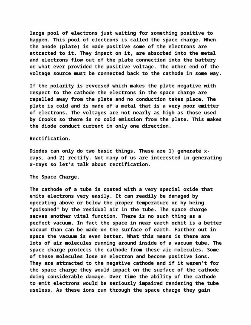
By applying Kirchhoff's and Ohm's laws to the circuit of Figure 4.2 it is possible to write some other equations. Summing currents we have
IE = IC + IB (4.2) where IE is the emitter current. Summing voltages around the base loop we have
VBB = IB RB + VBE (4.3) where VBE is the base to emitter voltage drop, which is approximately 0.6 volts. If we substitute VBE = 0.6 v and rearrange equation 4.3 we have
IB = (VBB - 0.6 v) / RB (4.4) In the collector loop we can write
VCC = IC RC + VCE (4.5) where VCE is the voltage between collector and emitter. In a great many circuits VCE is taken as the output voltage of the transistor circuit. Rearranging equation 4.5 we have
VCE = VCC - IC RC (4.6) If we combine equations 4.1, 4.4 and 4.6 we have
VCE = VCC - beta RC (VBB - 0.6 v) / RB (4.7) VCE can never, repeat NEVER, change sign. The absolute value of VCC must always be greater than the absolute value of VCE in equation 4.7. VCE can never exceed VCC because to do so would require that the term on the right in equation 4.7 undergo a change of sign. That cannot happen in the real world. Because the base-emitter junction is a P-N junction diode, if VBB becomes less than 0.6 volts, the base current will simply stop, not reverse. VCE
will be equal to VCC.
Within the limits 0 to VCC notice that if VBB is decreased, VCE is increased and visa versa. These are common emitter equations and may not apply to all circuits employing bipolar transistors.
The important thing about these seven equations is to understand how they were obtained. If you do not understand how these equations were obtained it is guaranteed that the rest of this chapter will be Greek to you.
4.2 The BJT as a Switch.
As mentioned above if the base current is removed from a transistor, the collector current will become similar to the reverse current in a diode, (too small to measure). Thus if a small current is turned on and off in the base of a BJT, the collector current will be turned on and off. Because the collector current is much larger than the base current, a low power circuit can be made to turn a high power device on and off. An excellent example of this is an indicator light.
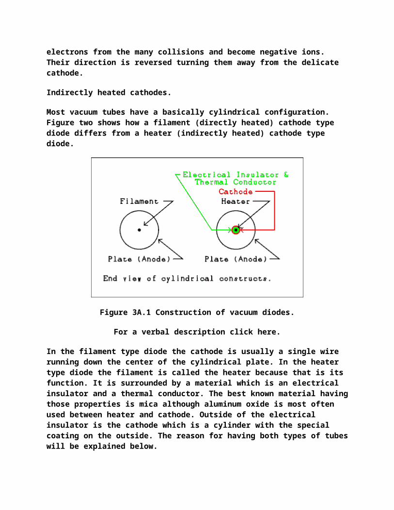
Figure 4.3 BJT Switch Turns Light On and Off
For a verbal description click here.
Figure 4.3 shows how a transistor can be used to turn a light on and off. It is very common in both consumer and laboratory equipment for a light to come on to indicate that a particular function has been activated. The input terminals on the left connect to what will be referred to as the driving source. The driving source is not capable of delivering enough current to light the lamp. This low power circuit will deliver a voltage when the light is to be on and no (or very little) voltage when the light is to be off.
An ideal switch has infinite resistance when it is open and zero resistance when it is closed. The BJT is quite close to being ideal in the open (off) condition but in the closed (on) condition it is not quite perfect. The on condition is known as saturation and is the condition wherein the collector current is as large as it can be. When a transistor is in saturation VCE is about 0.1 or 0.2 volts.
When a BJT is in saturation, most of the power supply voltage will appear across the load (device being switched on and off) and so the current through the load is
ISAT = (VCC - VCESAT) / RL (4.8)
where VCC is the power supply voltage, RL is the load resistance and 0.1 v < VCESAT < 0.2 volts.
Example 4.1.
A lamp having a resistance of 22 ohms is to be switched by a BJT. The power supply voltage is 5 volts and the collector saturation voltage is 0.1 volts. What is the saturation current of the transistor? See Figure 4.3.
Solution:
ISAT = (5 v - 0.1 v) / 22 ohms = 223 mA
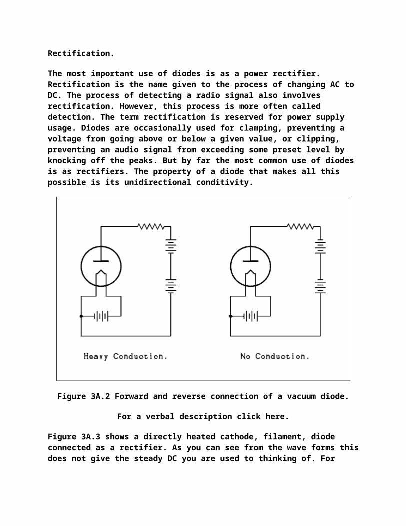
Trouble can develop in switching circuits if the transistor is not in saturation. To place a transistor in saturation it is necessary to supply more base current than is needed to just barely place the transistor in saturation. To be absolutely certain that the transistor is in saturation, the base current should be at least twice that required to just barely saturate the transistor. It will not do any damage if the base current is larger than that required for saturation. The collector current cannot be any greater than the saturation current.
Example 4.2.
Using the same conditions from example 4.1, what is the minimum base current required to place the transistor in saturation if beta is 80?
Solution:
IBMIN = ISAT / beta = 223 mA / 80 = 2.79 mA
The resistor in the base circuit must be properly selected so as to cause the base current to be large enough to place the transistor in saturation. On the other extreme the driving source will have a practical limit to how much current it will supply. If there were no limit, the load could be connected to the source and the switching transistor would not be needed.
Example 4.3.
Continuing with examples 4.1 and 4.2, what is the range of resistance for RB if the driving source can supply a maximum of 12 mA at a voltage of 5 volts. What should the resistance be to give a saturation safety factor of 2.5?
Solution:
In example 4.2 the minimum base current was calculated to be 2.79 mA. The maximum base current is the maximum which the driving source can supply, which is given as 12 mA. Solving equation 4.4 for RB we have
RB = (VBB - 0.6 v) / IB
RBMIN = (5 v - 0.6 v) / 12 mA = 367 ohms.RBMAX = (5 v - 0.6 v) / 2.79 mA = 1.58 k ohms.Since the minimum base current for saturation is 2.79 mAa safety factor of 2.5 calls for a base current of 6.98mA. RB = (5 v - 0.6 v) / 6.98 mA = 630 ohms.A 620 ohms standard value resistor would be used.
Another consideration in switching transistor circuits is whether the transistor will be turned off when it is supposed to be off. As long as the voltage of the driving source goes below about 0.6 volts, the transistor will most likely be turned off. But some driving sources do not go below 0.6 volts and the transistor may not be completely turned off.
Example 4.4.
In Figure 4.3 it is now assumed that VCC is 5 volts, the resistance of the lamp is 22 ohms, the resistance of RB is 620 ohms and the beta of the transistor is 80. The driving source has an "on" voltage of 5 volts. (a) If its "off" voltage is 0.2 volts, is the transistor off? If not, what is the collector current? (b) If the driving source has an "off" voltage of 1.0 volts, is the transistor off? If not, what is the collector current?
Solution:
(a) The driving source has an "off" voltage of 0.2 volts. That is less than the 0.6 volt breakdown of the base-emitter junction. There will be no base current and so there will be no collector current. The transistor switch will be off. (b) If the "off" voltage of the driving source is 1 volt there will be some base current. The base current will be IB = (1 v - 0.6 v) / 620 ohms = 0.645 mA; the collector current will be 80 x 0.645 mA = 51.6 mA. Although they are not asked for in the original example we will calculate the drop across the load and VCE to give a complete illustration of this type of problem. The drop across the load is IC RL = 51.6 mA x 22 ohms = 1.14 volts. VCE is VCC - VL
= 5 v - 1.14 v = 3.86 volts.
As you can see in the above example the transistor is "mostly" off. The lamp would glow slightly. An operator might be confused and become unsure as to whether a particular function is engaged or not. In something such as a nuclear power plant such confusion could be the difference between safe and unsafe operation. It is highly undesirable for indicator lamps to be partially on when they are supposed to be off.
Figure 4.4 shows a circuit which will overcome the problem of a driving source which will not go to zero for the off state.
Figure 4.4 Switching Circuit for Non-zero Driving Sources
For a verbal description click here.
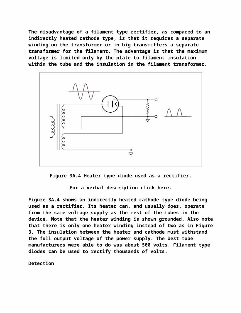
The procedure for solving this circuit is as follows. 1. Assume that there is no load on the voltage divider in the base circuit and see if the
transistor will be turned on or not. If the calculated voltage exceeds 0.6 volts, the transistor is at least part way on. If the voltage is less than 0.6 volts the transistor is off.
2. To calculate the base current in the "on" state assume that VBE is 0.6 volts and calculate the current through R2 (the voltage across R2 will be 0.6 volts).
3. Calculate the current through R1 assuming VBE to be 0.6 volts. 4. The current through R1 will split. Some will go through R2 and the rest will go into
the base of the transistor. To obtain the base current subtract the R2 current from the R1 current.
For those who would rather memorize an equation it is
IB = (VDSON - 0.6 v) / R1 - 0.6 v / R2 (4.9)
where VDSON is the on voltage of the driving source. It should be pointed out and emphasized that VBE for a good (not burned out) BJT can never exceed about 0.6 or 0.7 volts. If it does in a calculation, something has been neglected but no damage is done. If VBE
exceeds 0.7 volts in the real world, the BJT is burned out. If it wasn't before, it is now.
Example 4.5
For the values given in Figure 4.4 will a driving source which has an on voltage of 5 volts and an off voltage of 1 volt turn the BJT switch on and off?
Solution:
For the off state VBE = 1 v x 1 k ohms / (5.6 k ohms + 1 k ohms) = 0.15 v; the BJT switch is off. For the on state VBE = 5 v x 1 k ohms / (5.6 k ohms + 1 k ohms) = 0.76 v; there will be base current. Calculating the amount of base current
IB = VDSON - 0.6 v) / R1 - 0.6 v / R2 = 4.4 v / 5.6 k ohms - 0.6 v / 1 k ohm = 0.186 mA
The base current required to turn the switch on is IB = IC / beta and IC = RC / VCC = 12 v / 150 ohms = 80 mA, IB = 80 mA / 100 = 0.8 mA. With 0.8 mA required and 0.186 mA supplied, there is insufficient base current to turn the BJT switch on.
Example 4.6
Will a driving source of 10 volts turn the BJT on in Figure 4.4?
Solution:
We know from example 4.5 that 5 volts is enough to slightly forward bias the base-emitter junction and so we do not need to test to see if 10 volts will do it. Calculating IB gives
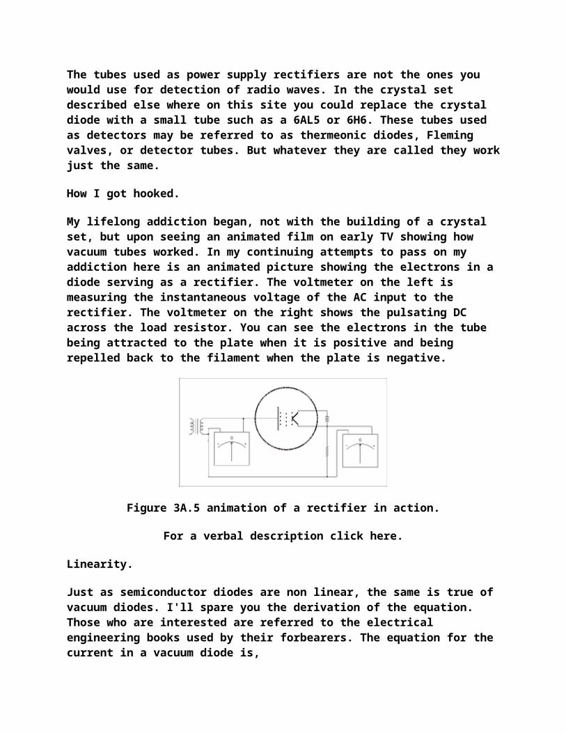
IB = (10 v - 0.6 v) / 5.6 k ohms - 0.6 v / 1 k ohm = 1.08 mA.
In example 4.5 we saw that 0.8 mA was required to turn the BJT on and we have 1.08 mA. The BJT is on.
BJT switches are used whenever a device such as a microprocessor needs to switch the current to any device which draws more current than the microprocessor can supply. Devices which may be switched include lamps, relays, buzzers and digital displays.
4.3 The BJT as an Amplifier.
An amplifier is any sort of device which will increase the magnitude of a signal. An amplifier may increase the magnitude of the voltage, current or both but to qualify as a true amplifier it must increase the power of a signal. A transformer can be used to increase the voltage of a signal, but there is no increase in power and a transformer is not an amplifier.
To characterize an amplifier completely it is necessary to know four things about it. They are
1. the relationship between the input voltage and the input current, 2. the relationship between the output voltage and the output current, 3. a relationship showing how the output is affected by the input, and 4. a relationship showing how the input is affected by the output.
These characteristics are called the four-terminal network parameters.
There are three groups of parameters, the impedance parameters, the admittance parameters and the hybrid parameters. All four of the impedance parameters have units of ohms and all four of the admittance parameters have units of ohms-1. The hybrid parameters are a mix of units.
Figure 4.5 Generalized Four-terminal Network
For a verbal description click here.
Figure 4.5 shows a generalized four-terminal network. The open circuit impedance parameters are as follows.
Input Impedance Z11 = V1 / I1 with I2 = 0 Output Impedance Z22 = V2 / I2 with I1 = 0 Forward Transfer Impedance Z12 = V2 / I1 I2 = 0 Reverse Transfer Impedance Z21 = V1 / I2 I1 = 0
"What has all of this to do with transistors?" A transistor can be treated as a four-terminal network. "Hold on now, you said a transistor has three terminals, emitter, base and collector, I remember that!" Correct. We will use one of the terminals twice so as to use four-terminal network parameters on a BJT.
Let us apply the hybrid parameters to the common emitter configuration. That means that the input is applied between the base and emitter and the output is taken between the collector and emitter as indicated in Figure 4.6a.
In the equations to follow all of the voltages and currents are AC small signal. Small signal means that the AC voltages are small enough so that the natural nonlinearities of P-N junctions are not significant and the I-V characteristics "look" linear. This is not an unrealistic condition. All amplifier transistors must be used in this way to avoid signal distortion. Distortion is any unwanted alteration of the signal.
The small-signal common-emitter hybrid parameters for the BJT are as follows.
The short-circuit input impedance.
hie = vbe / ib with v ce = (4.10) 0 The open-circuit output admittance.
hoe = ic / vce with i b = 0 (4.11) The short-circuit forward current transfer ratio.
hfe = ic / ib with v ce = 0 (4.12) The open-circuit reverse voltage transfer ratio.
hre = vbe / vce with i b = 0 <(4.13) Just in case you are wondering, hre is measured by injecting a signal at the collector and making a measurement at the base. These parameters are all definitions.
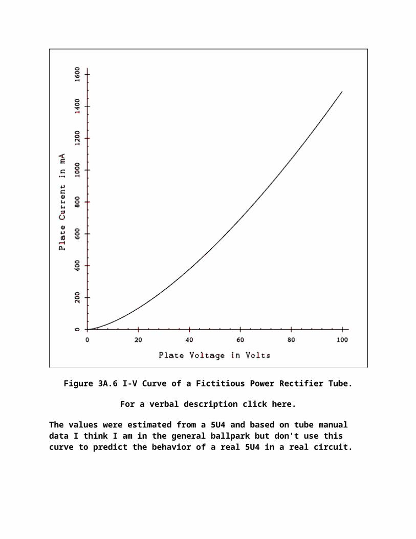
Figure 4.6 (a) BJT and (b) Four-terminal Equivalent Circuit.
For a verbal description click here.
The hybrid parameters give rise to the equivalent circuit of Figure 4.6b. This circuit takes the place of the transistor and is considered to be equivalent to it. The parameter hie is the input resistance. It is connected in series with the voltage generator which represents hre. The presence of hre indicates that a small amount of the output voltage is fed back into the base-emitter loop. In the collector-emitter loop a resistor representing hoe and a current source representing hfe are connected in parallel. Although hoe is expressed as a conductance, it is the reciprocal of the output resistance of the transistor. The current produced by the current source hfe is equal to hfe times the current in the base loop.
A generator may be connected, (in thought), to the base- emitter side of the equivalent circuit and a load resistance connected to the collector-emitter side. Equations may then be derived for such things as the input impedance, the output impedance and the gain. These equations are indeed complex. Advancing technology has saved us from having to deal with these equations.
The voltage feedback which is represented by hre is caused by the electric field within the transistor which is produced by the collector-to-emitter voltage. This field affects the concentration of charge carriers within the base and causes the forward voltage drop across the base-emitter junction (VBE) to be affected by the magnitude of VCE. The same electric field causes the collector current to increase as VCE increases. The value of hoe is the slope of the graph of IC versus VCE. Modern transistor design has overcome both of these problems to a very large extent. The amount of output voltage which is fed back to the input side is negligible in modern transistors and hre can be neglected and removed from the equivalent circuit. With modern transistors the graph of IC versus VCE is a horizontal line for voltages above about 1.5 volts. A horizontal line has a slope of zero and if hoe is zero, the output resistance is infinity. An infinite output resistance means that the resistor representing hoe may be removed from the circuit.
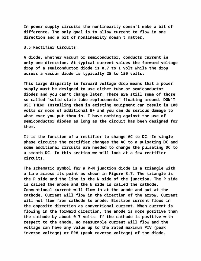
Figure 4.7 Simplified Equivalent Circuit.
For a verbal description click here.
The simplified equivalent circuit is shown in Figure 4.7. The equivalent circuit consists of the resistor labeled hie and the current source labeled ib> hfe. To make use of this circuit we must connect a couple of things to it. A Thevenin's equivalent circuit of a generator is connected to the B and E terminals. A load resistor is connected to the C and E terminals. We will use this circuit to derive the equations for gain and input impedance.
The current in the first loop is simply,
ib = vbe / hie (4.14)
The output voltage is, vce = - hfe ib RL (4.15)
The minus sign in equation 4.15 arises from the fact that the current in the current source is flowing downward and so it is flowing upward in the load resistor. If we now substitute equation 4.14 into equation 4.15 and divide by vbe we obtain,
vce / vbe = - (hfe RL ) / hie (4.16) If we define the voltage gain as AV = vce / vbe then we have
AV = - (hfe RL ) / hie (4.17) The input impedance of a common emitter amplifier is equal to Hie. The output impedance is virtually infinite.
Example 4.7
A BJT has the following parameters, hfe = 90 and hie = 4 k ohms. If this transistor is placed in a circuit where the load resistance is 4.7 k ohms, what is the voltage gain of the circuit?
Solution:
AV = - (hfe RL ) / hie = - ( 90 x 4.7 k ohms ) / ( 4 k ohms ) = 106
The solution to example 4.7 indicates that the amplifier in question will have an output voltage 106 times as large as its input voltage and the phase of the output signal will be inverted. 180 degrees phase shift.
Biasing the Bipolar Transistor.
The BJT is normally used to amplify small AC signals but it won't do anything unless it is provided with the proper DC voltages and currents. The process of providing the DC values is called biasing. One way to bias a transistor is as shown in Figure 4.2. The combination of VBB and RB will provide a constant DC current to the base. The collector current should be adjusted such that 1/2 of VCC is dropped across RC. VCE will also be 1/2 of VCC. This condition permits the AC output signal to be as large as it can possibly be. The collector voltage can "swing" from 0 to VCC. This type of biasing is never used in practical circuits because the collector current depends on the value of the DC beta of the transistor. The value of beta changes with temperature and is different for different transistors even of the same type number.
Figure 4.8 Practical Audio Frequency Amplifier.
For a verbal description click here.
A complete practical one-stage audio frequency amplifier is shown in Figure 4.8. Approximately 2 volts DC are dropped across the emitter resistor which leaves a 10 volt range for VCE (2 volts to 12 volts). The static collector voltage is halfway between 2 and 12, which is 7 volts. The voltage at the base is approximately 2.6 volts. Capacitor C1 is
necessary to prevent this voltage from interfering with the operation of or possibly even damaging the device which is to provide the signal to the amplifier. C3 blocks the DC at the collector from reaching the circuits or devices which may be connected to the output of the amplifier. R5 provides a charging path for C3 to make sure that there is no DC voltage present at the output even though there is no other load connected. Remember back in chapter 2 when we were talking about mixtures of AC and DC? Well, here it is. The RC networks are used just as described to pass the AC while blocking the DC.
The purpose of C2 requires a bit more explanation. If C2 were not present, the gain of the amplifier would be considerably reduced. It works this way. When the input signal goes positive, the base current increases and so does the emitter current. That increases the voltage drop across the emitter resistor and reduces the effect of the increasing signal. The effect of the signal could not be completely canceled out because, if the change in emitter current were completely canceled out, there would be no change in emitter current to cancel out the change in base current. The effect of the changing input signal is considerably reduced, which considerably reduces the gain of the circuit. Connecting C2 from the emitter to ground will prevent rapid changes in the emitter voltage and so the input signal will not have its effect reduced by any changes in the emitter voltage. The process of reducing the effective gain by removing the emitter bypass capacitor C2 is called emitter degeneration and, as we will learn in the next chapter, is not necessarily a bad thing.
Operating Point Stability
The set of conditions, IC, VCE, etc., are referred to collectively as the operating point. The operating point of a transistor must be stabilized against two types of changes. 1) The temperature can change and the value of beta is very temperature dependent. 2) Changing transistors, transistors can and do burn out and have to be replaced. The replacement most likely will not have the same value of beta as the original unit. There is no guarantee that a circuit will always be operated at room temperature. Air conditioning and heating systems can break down; portable devices can be carried outside on a summer or winter day. A device which fails to operate if the temperature gets above 85degrees or below 65degrees will not be very useful. If a transistor burns out it must be replaced to restore operation. Even if the replacement transistor has the same number as the original transistor, its beta may differ by as much as 30% from the original. If the circuit is not properly designed, the circuit may not work following the replacement of a defective transistor.
If the circuit of Figure 4.2 were used as an amplifier (and it could be) it would suffer from both problems described above. The circuit of Figure 4.8 does not suffer from these problems and here is why. The base current is small compared to the current flowing down through R1 and R2. The voltage divider which is constituted by R1 and R2 is lightly loaded and its output voltage will change only slightly as the base current changes. Suppose that the collector current tries to increase due to a temperature or a transistor change. The emitter current is IC + IB and IB is very much less than IC; therefore, IE is approximately equal to IC. As IC goes so goes IE. IE is trying to increase which will increase the voltage drop across RE which, in turn, will increase the voltage at the emitter. The voltage divider of R1
and R2 is holding the voltage at the base almost constant. An increase of emitter voltage while the base voltage is held constant will cause the forward bias on the base-emitter junction to be decreased and, therefore, decrease the base current. Remember we started out with the emitter current trying to increase which led to a decrease in base current. A decrease in base current will counteract the original increase in collector (emitter) current and the increase will not be as great as it would otherwise be. In fact, the emitter current will change only very slightly. If the collector (emitter) current tries to decrease, the voltage across RE will decrease, decreasing the emitter voltage while the base voltage is held constant. This increases the forward bias on the B-E junction and increases the base current which counteracts the decrease in collector (emitter) current.
If you were to set up the circuits of Figures 4.2 and 4.8 and put meters in the circuit to monitor the base and collector currents, you could see things happen. In the case of Figure 4.2 if heat were applied to the transistor the collector current would rise very rapidly. In the case of Figure 4.8 the collector current would change very slightly and the base current would drop off drastically. If the transistor were cooled, the currents would change in the opposite direction. A transistor with a higher beta will result in a larger collector current in the circuit of Figure 4.2 and a smaller base current in Figure 4.8.
The circuit of Figure 4.2 is called constant current biasing. It is never used in analog (as opposed to switching) circuits. The circuit of Figure 4.8 is called constant voltage biasing and it - or a variation of it - is used in all transistor circuits, including the internal circuitry of integrated circuits.
Circuit Analysis.
The circuit of Figure 4.8 is much easier to analyze if the voltage divider is replaced by its Thevenin's equivalent circuit as shown in Figure 4.9. Capacitors have been omitted because this is a DC analysis and capacitors are open circuits for DC. The values of VBB and RB are given by these equations
VBB = VCC R2 / (R1 + R2 (4.18) )
and
RB = (R1 R2) / (R1 + R2 (4.19) )
where R1 and R2 are the original base resistors as shown in Figure 4.8.
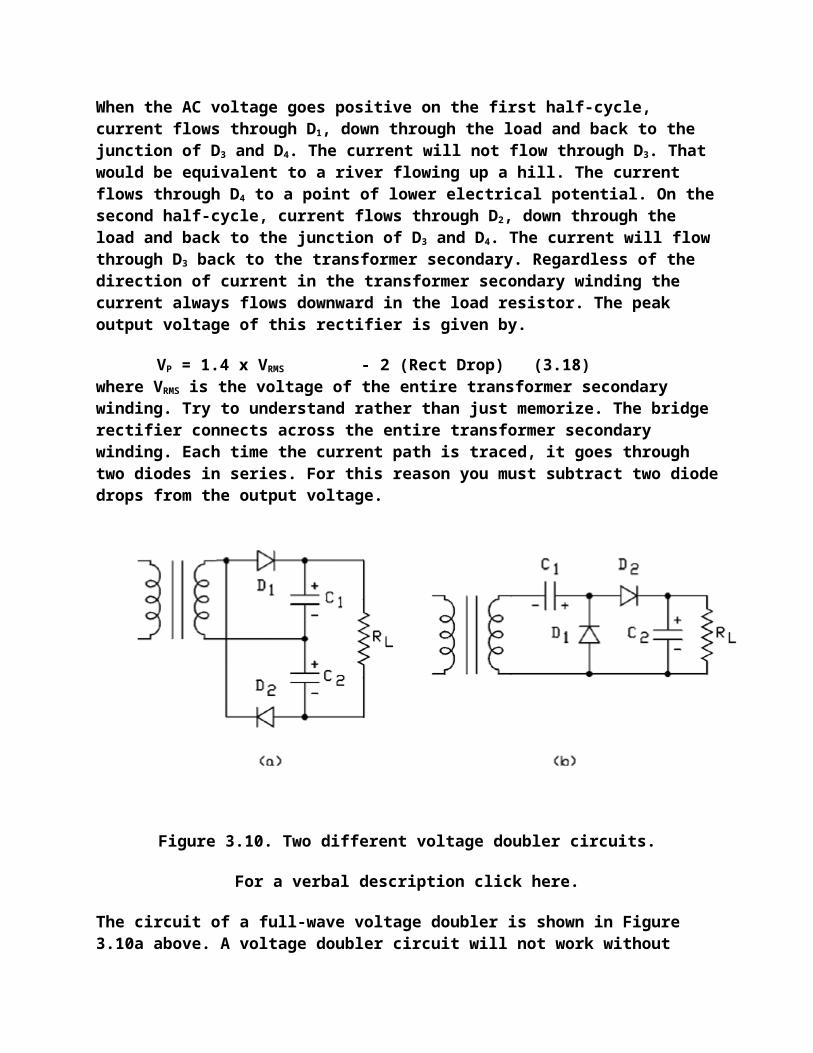
Figure 4.9 Thevenin's Equivalent Circuit Replaces R1 and R2
For a verbal description click here.
If equations 4.18 and 4.19 seem to have "come out of the blue," you need to review the section on Thevenin's equivalent circuit (section 1.3 pages 41 to 46).
We will now write the loop equations for the circuit of Figure 4.9. Summing voltages in the base loop gives
VBB = RB IB + VBE + RE (IB + IC (4.20) )
The voltage drop across RE (R4 in Figure 4.8) is IE RE but IE = IB + IC. The base current is given by
IB = IC (4.21) / beta
Substituting equation 4.21 into equation 4.20 and solving for IC gives
IC = beta (VBB - VBE) / (RB + RE (4.22) (1 + beta))
If beta is greater than 50 an error of less than 2% will be introduced by letting the (1 + beta) term in the denominator equal beta. Making this substitution and dividing through by beta we have
IC = (VBB - VBE) / (RE + RB (4.23) / beta)
Equation 4.23 is probably the best one to use to calculate the collector current of a constant voltage biased BJT.
It is possible to make a further approximation but it must be applied with great care. In the denominator of equation 4.23 RB / beta may be much less than RE. If this is true the following equation may be used.
IC = (VBB - VBE) / RE if and only if RB / beta << RE (4.24) .
Example 4.8
Calculate the values of VBB and RB for the circuit of Figure 4.8.
Solution:
VBB is the unloaded output of the voltage divider consisting of R1 and R2
VBB = VCC R2 / (R1 + R2) = 12 v x 6.8 k ohms / (22 k ohms + 6.8 k ohms) = 2.83 v
RB is the parallel combination of R1 and R2
RB = R1 R2 / (R1 + R2) = 22 k ohms x 6.8 k ohms / (22 k ohms + 6.8 k ohms) = 5.19 k ohms
Example 4.9
If the transistor in Figure 4.8 has a beta of 150, what is the collector current?
Solution:
Which equation should we use? Equation 4.22 is the most exact form but the difference between beta and beta + 1 is only 0.66%. We might use equation 4.24 but that one is usually used only when beta is not given and a typical value must be assumed. We will use equation 4.23.
IC = 2.83 v - 0.6 v / (1.8 k ohms + 5.19 k ohms / 150) = 2.23 v / (1.8 k ohms + 0.03 k ohms) = 1.22 mA.
If equation 4.24 had been used the error would have only been 1.67%, which is well within acceptable limits. Perhaps another example will illustrate when equation 4.24 should not be used.
Example 4.10
In a circuit similar to Figure 4.8 VCC = 15 v, R1 = 100 K ohms, R2 = 47 k ohms, R3 = 4.7 k ohms, R4 = 3.3 k ohms and beta = 50. What is the collector current?
Solution:
Since beta = 50 this is a borderline case for the 2% rule but we will ignore beta + 1 and use equation 4.23. VBB = 15 v x 47 k ohms / (100 k ohms + 47 k ohms) = 4.80 v and RB = 100 k ohms x 47 k ohms / (100 k ohms + 47 k ohms) = 32.0 k ohms.
IC = 4.80 v - 0.6 v / (3.3 k ohms + 32.0 k ohms / 50) = 4.20 v / (3.3 k ohms + 0.64 k ohms) = 1.07 mA.
The Common Collector (Emitter-follower) Amplifier.
If the collector of a BJT is placed at AC ground potential while the input signal is applied between ground and base and the output signal is taken between ground and emitter, the collector is common to input and output. Such an amplifier is a common collector configuration but is commonly known as an emitter-follower. An AC coupled emitter-follower is shown in Figure 4.10.
Figure 4.10 AC Coupled Emitter-follower.
For a verbal description click here.
The reason it is called an emitter-follower is because of that nearly constant 0.6 volt drop from base to emitter. How ever the base voltage may change, the emitter voltage is following along only 0.6 volts behind. To put it more precisely, for an NPN transistor the emitter voltage is 0.6 volts less then the base voltage. For a PNP transistor the emitter voltage is 0.6 volts greater than the base voltage. That 0.6 volts may not be important in the circuit of Figure 4.10 but in a DC coupled emitter-follower it may be very important.
The AC gain of an emitter-follower may be derived using the familiar common emitter parameters by drawing the equivalent circuit as in Figure 4.11. This circuit is a little difficult to follow (pun fully intended) and so the wires have been untangled in Figure 4.12. In equivalent circuits it is customary to omit DC biasing and capacitors because they add nothing to the AC circuit.
Figure 4.11 Common Collector Equivalent Circuit.
For a verbal description click here.
Figure 4.12 Figure 4.11 with Wires Untangled.
For a verbal description click here.
Writing a loop equation around the outside loop gives vin = ib hie + vo . (4.25)
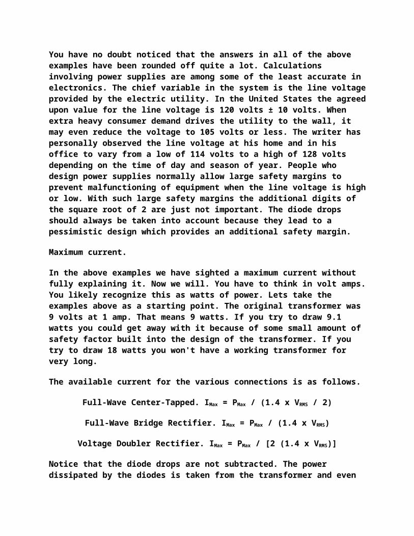
We will make the approximation that the base current ib is much less than the collector current ic, and the emitter current will be considered equal to the collector current. The current flowing through RL is the collector current hfeib and we have
vo = ib hfe RL . (4.26)
If we solve equations 4.25 and 4.26 for ib and set them equal we have
vo / (hfe RL) = (vin - vo) / hie (4.27)
Solving this equation for vo / vin and remembering that voltage gain is defined as vo / vin we have
AV = hfe RL / (hie + hfe RL (4.28) )
Example 4.11.
A BJT has the following parameters, hie = 4 k ohms and hfe = 100. In an emitter-follower with a load (emitter) resistor of 1 k ohms, what is the voltage gain?
Solution:
AV = hfe RL / (hie + hfe RL) = 100 x 1 k ohm / (4 k ohms + 100 x 1 k ohm) = 0.962 The voltage gain of an emitter-follower is always slightly less than one. You may be wondering what use is an amplifier which slightly reduces the amplitude of the input signal. An emitter-follower has current gain. The current gain is equal to beta. For example, if you have a generator which can only supply 1 mA and you need to drive a load which requires 100 mA, an emitter-follower employing a BJT with a beta (or hfe) greater than 100 will allow the generator to drive the load provided there are no other losses in the circuit.
Input Resistance.
The input resistance of an emitter-follower is Rin = vin / ib (4.29)
If we rearrange equation 4.26 we have
vo / ib = hfe RL (4.30)
Because the gain of an emitter-follower is approximately unity, vo = vin. Combining this approximation with equations 4.29 and 4.30 we have
Rin = hfe RL (4.31)
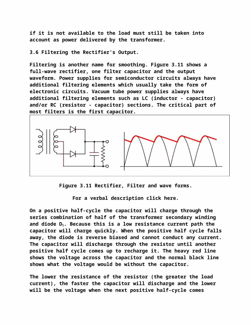
The value of RL is the parallel combination of all resistances connected from the emitter to ground.
Example 4.12.
In the circuit of Figure 4.13 an emitter-follower is being used to drive an 8 ohm speaker. If R1 = R2 = 390 ohms, R3 = 15 ohms, beta = hfe = 75 and hie = 5 ohms, what are (a) the voltage gain and (b) the input resistance?
Figure 4.13 Emitter-follower Driving a Speaker
For a verbal description click here.
Solution:
(a) The gain is given by equation 4.28. RL in this equation is the parallel combination of R3 and the 8 ohm speaker which is 5.22 ohms.
AV = hfe RL / (hie + hfe RL = 75 x 5.22 ohms / (5 ohms + 75 x 5.22 ohms) = 0.987
(b) The input resistance is the parallel combination of the two 390 ohm resistors in the base circuit and the input resistance of the emitter-follower. The input resistance of the emitter-follower is given by equation 4.31.
Rin = hfe RL = 75 x 5.22 = 392 ohms
The total input resistance is the parallel combination of 390 ohms, 390 ohms and 392 ohms which is 130 ohms
Resistances in Parallel.
Some of you may be puzzled over why resistors are being treated as if they are connected in parallel when they are not connected to the same point in the circuit. If you are not puzzled, you may skip this section.
For example, the speaker and the 15 ohm resistor R3 have been treated as if they are in parallel when it is obvious that there is a capacitor connected between them. We are talking about AC not DC. The job of the capacitor is to block DC and pass AC to the speaker. The value of the capacitor has been chosen such that its reactance is small at the lowest frequency to be passed to the speaker. The capacitor is essentially a short circuit for AC. When the capacitor is replaced by a short circuit the speaker and the 15 ohm resistor are in parallel.
The two 390 ohm resistors in the base appear more like they are in series than in parallel. The AC signal is applied to the junction of the two resistors. One of the resistors goes to ground and the other one goes to the power supply (VCC). Within the power supply is a large capacitor connected from VCC to ground, or a voltage regulator, most likely both. For AC there is a short circuit connected from VCC to ground, which means that connecting a resistor to VCC is the same as connecting it to ground as far as AC is concerned. The input resistance of the transistor appears from base to ground and so is in parallel with the resistors in the base circuit.
Output Resistance.
To determine the output resistance of an emitter- follower we rearrange the equivalent circuit of Figure 4.12 and redraw it in Figure 4.14.
Figure 4.14 Measuring Output Resistance of Emitter-follower.
For a verbal description click here.
The generator has been removed from the input and replaced by its internal resistance Rg. The load resistor has been removed and a generator has been connected to the output. The purpose of this is to apply a known voltage to the output and see how much current flows.
This can be done in the laboratory if care is taken not to drive the transistor into nonlinear regions of its I-V characteristic.
Summing the voltage drops around the outside loop gives
ib (Rg + hie (4.32) ) = V.
The current flowing in the generator is
I = ib (hfe (4.33) + 1).
Eliminating ib between equations 4.32 and 4.33 and rearranging yields
V / I = (Rg + hie) / (hfe + 1) (4.34)
Since RO = V / I we have
RO = (Rg + hie) / (hfe + 1) (4.35)
Example 4.13.
In the circuit of Figure 4.13 calculate the output resistance which is effectively connected across the speaker. The output resistance of the generator is 50 ohms.
Solution:
The output resistance at the emitter of the transistor is given by equation 4.35. Rg must be the parallel combination of the generator resistance and the two resistors in the base circuit, 50 ohms in parallel with two 390 ohm resistors, which is 39.8 ohms
RO = (Rg + hie) / (hfe + 1) = (39.8 ohms + 5 ohms) / (75 + 1) = 0.589 ohms
The true output resistance is RO in parallel with 15 ohms but it isn't going to make much difference.
Rout = 15 ohms x 0.589 ohms / (15 ohms + 0.589 ohms) = 0.567 ohms.
Determining Transistor Parameters.
Transistor parameters may be found in a data sheet for the particular transistor or in a transistor data book. Data sheets for individual transistors may be obtained from the manufacturer often free of charge or for a nominal fee. These data sheets give all of the information you could possibly want. Data sheets give a range of values for each parameter. Whether you use an average value or the minimum value will depend on what you are trying to do.
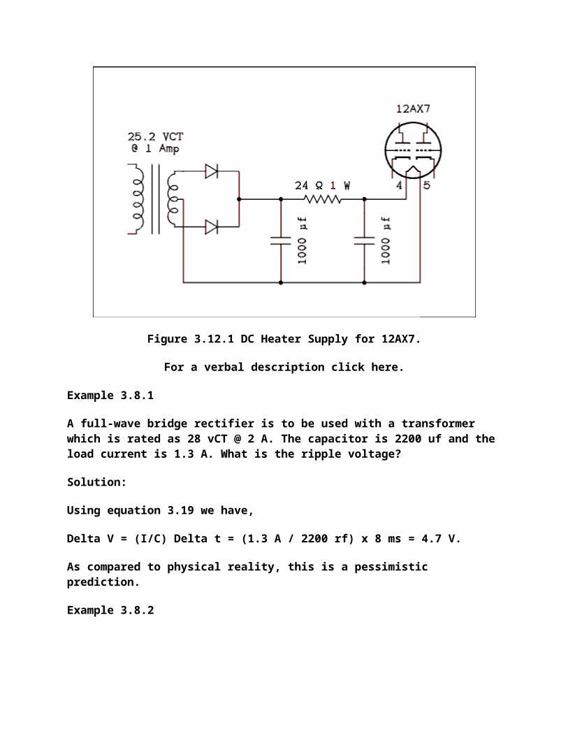
Most data books do not give a value for hie at all. They usually give a range of values for the current gain. For audio frequencies the values of beta and hfe are the same. It is unusual for a data book to give a value of hfe at high frequencies.
If you need to know the value of hie and you can't find it anywhere you can estimate it. Hie = 25 mv / IB. Since IB = IC / beta hie can be estimated as
Hie = 25 mv x beta / IC (4.36)
4.4 The Field Effect Transistor (FET).
There are two classes of field effect transistors, junction field effect transistors, JFETs, and metal oxide semiconductor field effect transistor, MOSFETs. We will begin with JFETs.
The Junction Field Effect Transistor.
Figure 4.15 Junction Field Effect Transistor.
For a verbal description click here.
Figure 4.15 shows an N channel junction field effect transistor (JFET). If a battery is connected to the ends of the channel, (source and drain) current will flow as if it were a resistor. Like any other resistance device the resistance will depend on the length and cross-section area of the block of semiconductor material.
It is the cross-section area which is important in the JFET. If the gate to channel junction is reverse-biased the depletion region will grow outward from the gate as shown in Figure 4.16. As the depletion region grows larger the conduction cross-section area is decreased. The depletion region does not conduct current. As the reverse bias voltage on the gate-channel junction is increased, the resistance of the channel is increased. At comparatively large gate to channel voltages (about 10 volts) the channel resistance is approaching infinity. At a gate to channel voltage of zero the channel resistance is low, a typical value being 100 ohms.
Figure 4.16 JFET with Reverse Bias on the Gate.
For a verbal description click here.
Figure 4.17 JFET Showing Pinch-off Effect.
For a verbal description click here.
When a battery is connected across the ends of the channel, another effect becomes evident. Because the gate reduces the channel cross-section area, the resistance in the region of the gate is increased and most of the voltage which is applied will be dropped across the region occupied by the gate. This voltage drop causes the channel near the top of the gate (Figure 4.17) to be more positive than the channel near the bottom of the gate. The net voltage across the gate-channel junction is greater at the top than it is at the bottom. Hence, the depletion region will be wider at the top of the gate than it is at the bottom, as shown in Figure 4.17. As the voltage applied to the ends of the channel is increased, this effect is increased until the channel becomes a constant current device. The channel does not become a negative resistance device (current decreases as voltage increases). The voltage at which the channel changes from a resistive device to a constant current device is called the pinch-off voltage.
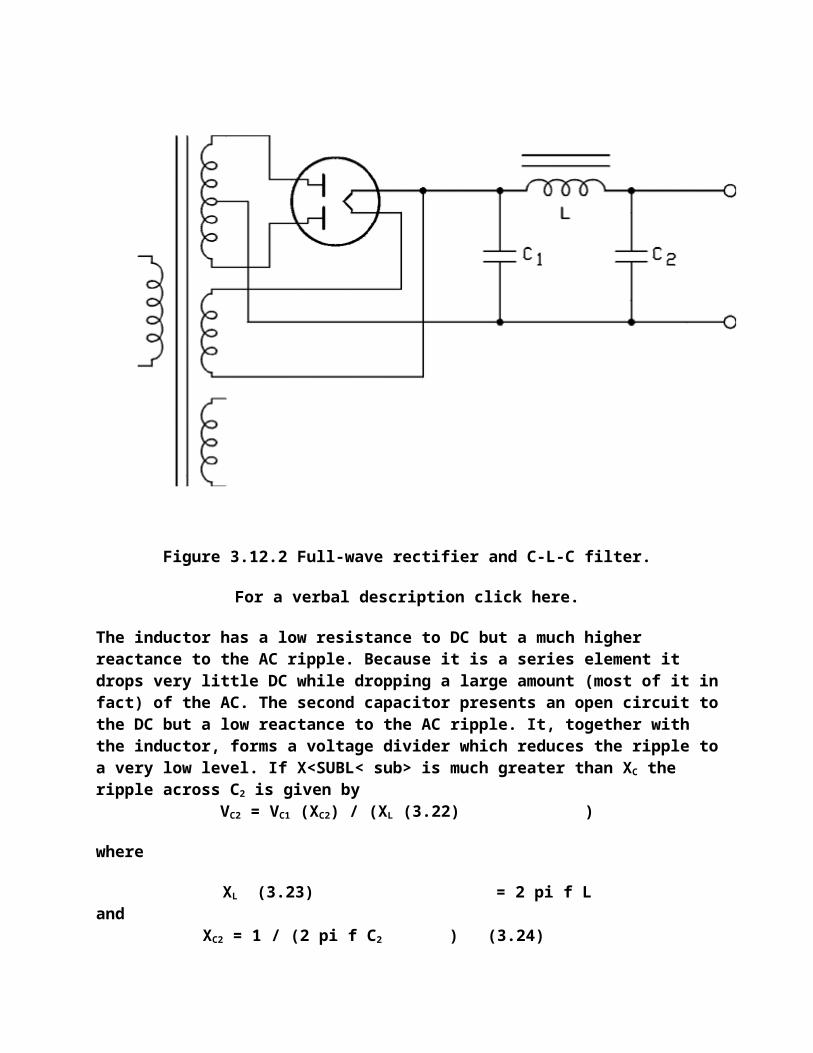
Figure 4.18 Drain Characteristics of a typical FET.
For a verbal description click here.
Figure 4.18 shows the drain characteristics of a typical junction field effect transistor. The semiconductor curve tracer in the laboratory will produce these curves on the screen of an oscilloscope. At drain-to-source voltages below the pinch-off voltage the drain-to-source path is a variable resistance while above the pinch-off voltage the drain-to- source path is a variable current source. Typical values for the pinch-off voltage are less than one volt.
The Metal Oxide Semiconductor Field Effect Transistor.
The metal oxide semiconductor field effect transistor (MOSFET) is at the heart of most pocket calculators and microcomputers. Its construction is quite similar to the JFET except that the gate is a metal plate which is insulated from the channel by a thin layer of silicon dioxide instead of a region of opposite type semiconductor.
The P-N junction in a JFET is not used as a diode. It operates in the reversed biased condition all of the time. The gate portion of the FET (P type semiconductor in the example shown) is only being used as a conductor. The depletion region on the gate side of the junction is being used as an insulator. Silicon dioxide is a much better insulator than is a reverse-biased P-N junction and metal is a better conductor than is P type semiconductor. So the replacements are made and the device works almost the same as it did before. In an N channel MOSFET if the gate is made negative with respect to the source the negative charge on the gate will repel negative charges in the semiconductor channel and create a
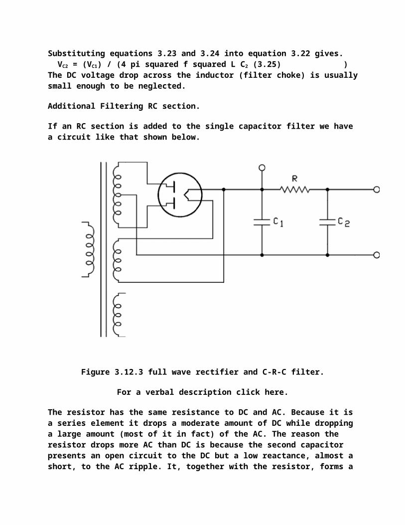
depletion region around the gate the same as with a JFET. The principle of pinch-off works the same way as well.
Figure 4.19 Metal Oxide Semiconductor FET.
For a verbal description click here.
The major difference between a JFET and a MOSFET is the gate or input resistance. For a JFET the typical input resistance is typically 1012 ohms while for a MOSFET the input resistance is typically 1016 ohms. MOSFETs are used in equipment which can measure currents in the picoampere range and below. Because of the high resistance of MOSFETs in a switching application, when they are off, they are really off. For this reason they find applications in very low power devices such as watches, calculators and lap-top computers.
The substrate is the foundation on which the MOSFETs are constructed. In the case of discreet MOSFETs (as opposed to integrated circuits) the substrate may be brought out to a connecting lead of its own so the user may connect it as desired. The substrate is usually connected to the source although a P type substrate may be connected to the most negative point in a circuit. When MOSFETs appear in an integrated circuit, the substrate is the foundation on which the IC is constructed.
Enhancement Mode MOSFETs.
MOSFETs can be divided into two groups, depletion mode and enhancement mode. The group we have been talking about up until now are the depletion mode type, so called because they work by creating a depletion region in the channel. Depletion mode MOSFETs are "on" at zero gate voltage and a negative gate voltage will turn them "off".
An enhancement mode MOSFET is "off" at zero gate voltage and a positive gate voltage (for an N channel) will turn it "on". The drawing of an enhancement mode MOSFET is shown in Figure 4.20.
Figure 4.20 Enhancement Mode MOSFET.
For a verbal description click here.
In the case of an N channel MOSFET the substrate is P type semiconductor. Near the gate (between the source and drain) the substrate has been doped with both donor and acceptor impurities. The acceptors slightly outnumber the donors so the result is a lightly doped P type semiconductor. When the gate voltage is zero the P type semiconductor between the source and drain serves to block current between source and drain. When a positive voltage is placed on the gate, holes are repelled away from the gate. Once the holes are gone from this region, the donor impurities predominate and the material near the gate turns from P type to N type semiconductor. Current may now flow from source to drain.
Enhancement mode MOSFETs are very rarely used as amplifiers. They most often appear in digital integrated circuits where they are used as switches.
Figure 4.21 Schematic Symbols for Various Kinds of FETs.
For a verbal description click here.
Figure 4.21 shows schematic symbols for the various kinds of FETs. The FETs in the top row are N channel and the FETs in the bottom row are P channel. A good memory device is "the arrow always points toward the N type semiconductor". The bottom connection on each FET is the source. The connection on the left of each FET is the gate and the connection at the top is the drain. For MOSFETs the connection at center-right is the substrate. The substrate is shown connected internally to the source in these symbols. In some discreet MOSFETs the substrate is brought to a separate lead.
For N channel FETs the drain is made more positive than the source. JFETs and depletion mode MOSFETs are fully on at zero gate potential. For operation as an amplifier, the gate is made more negative than the source. Enhancement mode MOSFETs are off at zero gate potential. For operation as an amplifier the gate is made more positive than the source.
For P channel FETs the drain is made more negative than the source. JFETs and depletion mode MOSFETs are fully on at zero gate potential. For operation as an amplifier, the gate is made more positive than the source. Enhancement mode MOSFETs are off at zero gate potential. For operation as an amplifier the gate is made more negative than the source.
4.5 The FET as a Switch.
FETs are usually not used to turn lamps and relay coils on and off. They find two major applications, as logic switches and as analog (or signal) switches. We will cover the latter application first.
The term analog switch may seem to be mutually contradictory. What is meant is to interrupt an analog signal to turn it off and on as desired or to select among several sources of signal. An example of the latter is the source selector in a stereo receiver. The switch allows the user to select among several program sources. Classically this has been accomplished by a mechanical switch. Newer designs which include remote control require electronic switching. This electronic switching may be accomplished using an FET.
Figure 4.22 shows an FET being used to switch an analog signal. The control voltage is +15 volts to turn the switch on and -15 volts to turn the switch off. The signal applied to the input must never exceed approximately plus or minus 10 volts. If the input signal comes too close to +15 volts, the switch can be turned off when it is supposed to be on. If the input signal comes too close to -15 volts, the switch can be turned on when it is supposed to be off.
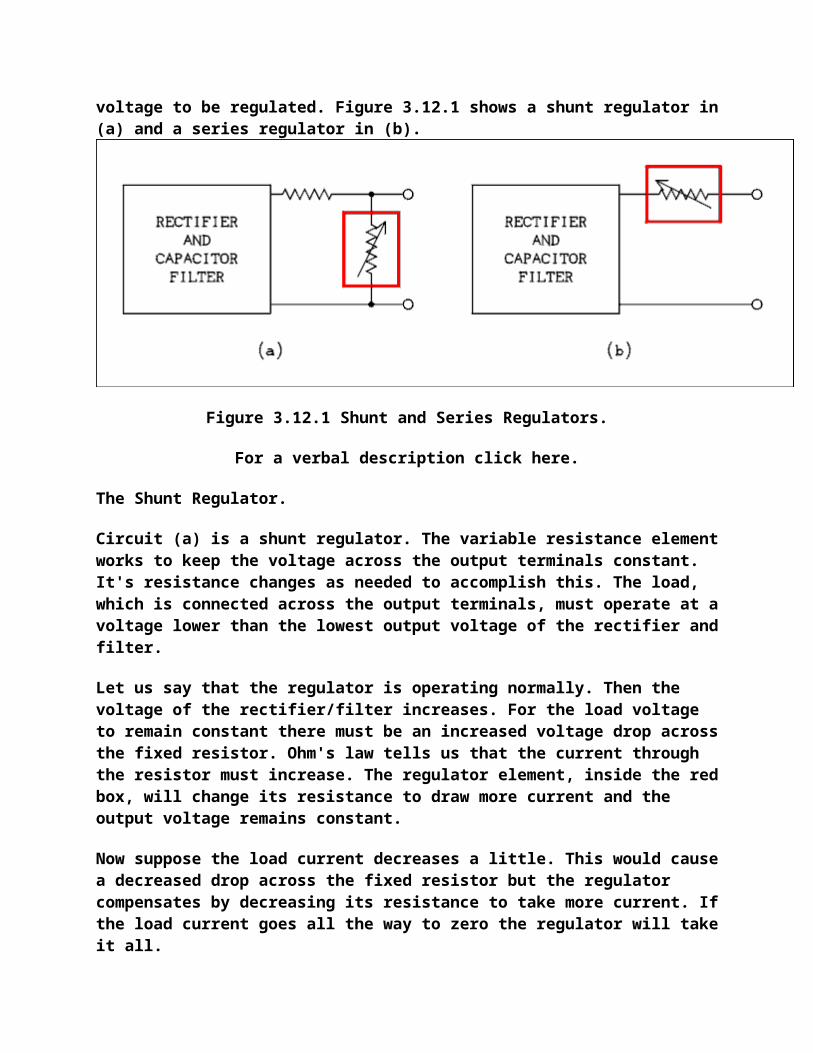
Figure 4.22 Analog Switch Using a JFET.
For a verbal description click here.
When the control voltage is positive, the diode is reverse biased, which disconnects the control voltage from the switched signal. The 100 k ohm resistor will cause the gate of the FET to be at the same potential as the source and the FET will be fully on. Signals applied to the input will appear at the output with little distortion or attenuation. When the control voltage is negative, the diode will be forward biased and the gate will be at approximately -15 volts. This will cause the FET to be turned off and very little or no signal from the input will be passed to the output. The 100 k ohm resistor will be connected from the -15 volt control signal to the signal source. In order for this circuit to work properly the signal source must have a low resistance for DC.
Another type of analog switch is the CMOS (complementary MOS) device which comes in an integrated circuit. The IC operates from a single power supply (VDD) of up to 15 volts. The signal source must never go negative nor more positive than VDD. It is best for the AC signal source to be added to a DC of 1/2 VDD. If the signal part of the switch is forced outside of these limits by more than 0.7 volts the IC will, not may, but will be destroyed. The control voltage for this IC is zero to turn the switch off and VDD to turn the switch on.
A partial schematic diagram of the internal workings of this IC switch is shown in Figure 4.23. The triangle with a circle on its nose is an inverter. This is a switching device. If its input is zero, its output is VDD. If its input is VDD, its output is zero.
Figure 4.23 MOSFET Analog Switch.
For a verbal description click here.
The circuit is called complementary because it employs an N channel and a P channel MOSFET. When the control voltage is zero, the N channel FET has a gate voltage of zero and the P channel FET has a gate voltage of VDD. That turns both of them off. If the signal source is at a potential of VDD the P channel FET will still be off and the N channel FET will be negatively biased, which makes doubly certain that it will be off. If the signal source is at zero potential the N channel FET will still be off and the P channel FET will be positively biased, which makes doubly certain that it will be off. When the control input changes to VDD the N channel FET has a positive VDD on its gate while the P channel FET has zero potential on its gate. If the signal is at zero potential the N channel FET will be on but the P channel FET will be off. If the signal is at VDD the P channel FET will be on, but the N channel FET will be off. The two FETs are in parallel. So as long as one of them is on, the switch is on.
The inverter is another example of how FETs are used as switches. Figure 4.24 shows the circuit of the inverter which was shown as a triangle in the circuit of Figure 4.23. When the input signal is at zero volts Q1 is biased fully on and Q2 is fully off. Thus the output is held to VDD. The output is high for a low input. If the input is VDD (high) Q1 is biased off (zero potential between gate and source) and Q2 is on. The output is low because it is held to ground by Q2. Whatever the state of the input, the output assumes the opposite state.
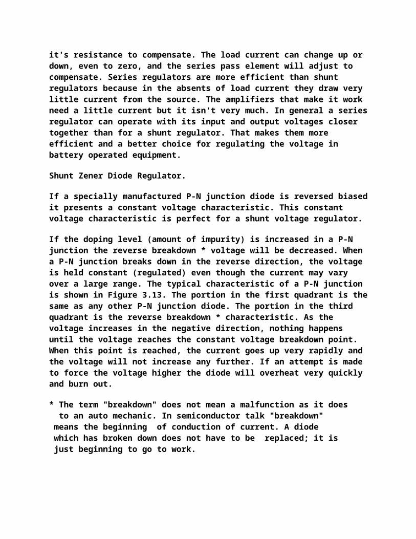
Figure 4.24 CMOS Inverter.
For a verbal description click here.
There are ICs which are known as invertors which contain six such circuits. Although they are not intended for use as analog devices, the input may be biased at 1/2 VDD and as such they make excellent amplifiers. (Which goes to show that if someone designs something, someone else will figure out a way to use it wrong and make it work.)
Example 4.14.
A P channel depletion mode FET has -10 volts on its gate with respect to its source. Is it on or off?
Solution:
A P channel depletion mode FET is on at zero potential and its drain current decreases as the gate is made positive. At +10 volts it would most likely be off but at -10 volts it is extremely on.
Example 4.15.
An N channel enhancement mode MOSFET has a gate bias of zero volts. Is this FET on or off?
Solution:
At zero volts between gate and source any enhancement mode MOSFET is off. The FET is off.
4.6 The FET as an Amplifier.
The FET has only two small-signal parameters, the drain resistance rd and the transfer conductance, called by contraction-loving electrical engineers transconductance Gm. The transconductance is defined as the AC drain current divided by the AC gate to source voltage with the drain to source voltage held constant.
Gm = id / vgs with vds = 0 (4.37) The drain resistance is defined as the AC drain to source voltage divided by the AC drain current with the gate to source voltage held constant.
rd = vds / id with vgs = 0 <4.38)
Figure 4.25 Small Signal Equivalent Circuit for an FET.
For a verbal description click here.
The Common Source Amplifier.
The common source equivalent circuit we will work from is shown in Figure 4.26. The input is an open circuit, as is the input of an FET. The output circuit consists of a current source which is dependent on the voltage between the gate and source. The drain resistance is in parallel with the current source. Any load is connected in parallel with the drain resistance.
Figure 4.26 Equivalent Circuit of Common Source Amplifier.
For a verbal description click here.
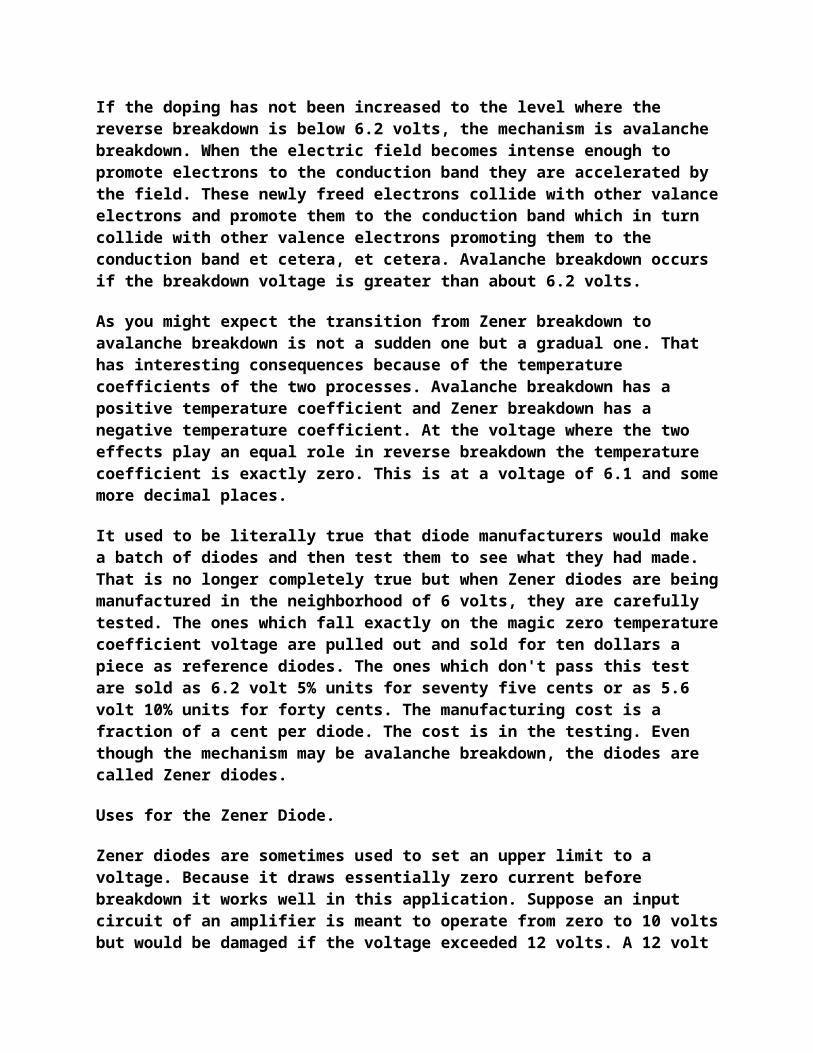
The output voltage vo is the current source times the parallel combination of rd and RL. vo = -vin Gm rd RL / (rd + R/L (4.19) )
Dividing through by vin and making the substitution AV = vo / vin we have, AV = -Gm rd RL / (rd + R/L (4.20) )
where RL is the parallel combination of all resistors connected from the drain to AC ground.
Amplifier Biasing.
A properly biased common source N channel JFET amplifier is shown in Figure 4.27. The battery VDD provides the positive bias for the drain and the battery VGG provides the negative bias for the gate. While this two-battery circuit will certainly work, it is not very practical.
Figure 4.27 JFET Amplifier Using Battery Bias.
For a verbal description click here.
Figure 4.28a shows how the circuit may be rearranged without altering its operation. The negative connection point of VDD has been moved to the negative end of VGG, reducing VDD
by the amount of VGG. This reduction is usually not significant enough to have any adverse effect. Notice that the polarity of VGG is the same as would be produced by the drain-source current flowing through a resistor in the source. Figure 4.28b shows the substitution of a resistor and a filter capacitor for the battery. The value of the source resistor sets the operating point.
Figure 4.28 Converting Battery Biasing to Self Biasing.
For a verbal description click here.
Unlike for the BJT the operating point of the FET cannot be easily calculated. Some texts present a graphical solution which requires having a set of characteristic curves for the FET similar to those in Figure 4.18. Semiconductor manufacturers do not supply these curves for a very good reason. There is so much difference between FETs of the same type number that a set of curves would be useless. A semiconductor curve tracer interfaced to a computer and plotter could produce a set of curves for any individual FET and the graphic solution could be performed. Such a solution would be valid for only that one particular FET. Another FET would require another set of curves and a new graphical solution. We will not waste our time learning a useless procedure.
The one and only advantage that FETs have over BJTs is their very high input resistance. In commercially designed equipment it is usual to see only one or two FETs among thirty or more BJTs. Even with such limited use, setting the operating point is a problem. There are two basic solutions. One is to use a trimming potentiometer (a screwdriver- adjusted variable resistor) as the source resistor as shown in Figure 4.29(a). Part of the calibration procedure includes setting the proper operating point of the FET amplifier. The other solution is to use the FET in conjunction with a BJT in an arrangement which will automatically set the operating point of the FET as shown in Figure 4.29(b).
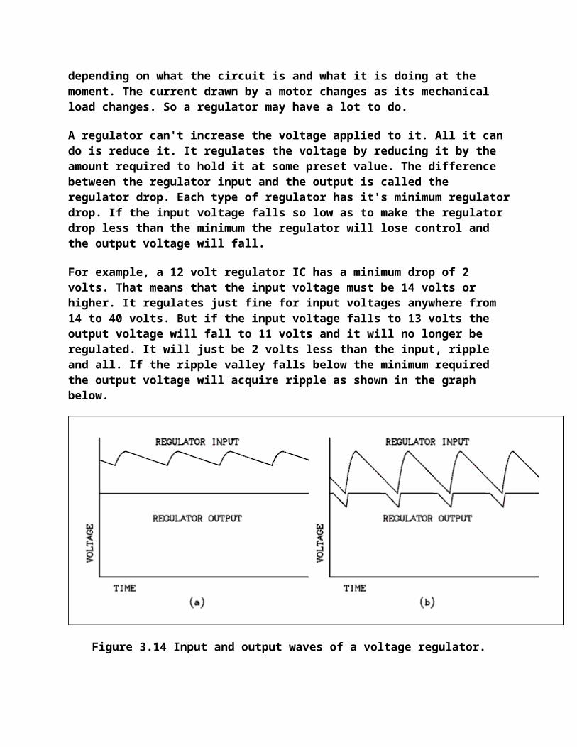
Figure 4.29 Practical JFET Amplifier.
For a verbal description click here.
Which one is used depends on who is to build the circuit. If the circuit is contained in a DIY article or a kit the reader or buyer is the one who constructs it. He does not receive a bill for his time at the end of each month so there is no cost associated with having him adjust the pot for the proper operating point.
If the circuit is in a device which will be manufactured in the tens or hundreds of thousands and sold in retail stores the eventual owner cannot be held responsible for adjusting the pot. It must be done on the assembly line by a worker. It is an unavoidable fact that workers have to be paid. It is also a fact that workers do occasionally make errors. The expense of paying someone to adjust the pot will buy a lot of transistors. While the circuit at (b) is mor costly in terms of parts it is less expensive when fabrication costs are taken into account.
The (b) circuit works because the BJT sets the current through both transistors and holds it constant. The collector voltage, also the source voltage adjusts itself to what ever value is necessary to make the FET conduct the correct amount of current. The gate resistor is returned to the base to insure that the BJT will never be forced into saturation by the required gate to source voltage of the FET. The gate resistor in either circuit can easily go as high as 10 meg ohms if necessary.
Example 4.16.
In the circuit of Figure 4.29 the drain resistance of the FET is 130 k ohms and the transconductance is 600 micro mhos. What is the amplifier gain?
Solution:
RL consists of the parallel combination of 47 k ohms and 100 k ohms, which is 32.0 k ohms. The gain of the amplifier is
AV = -Gm rd RL / (rd + RL)
AV = -600 micro mhos x 130 k ohms x 32 k ohms / (130 k ohms + 32 k ohms) = -15.4
The Source-follower Amplifier.
Because the FET is used for its high input impedance, it is most often seen as a source-follower, as shown in Figure 4.30. The FET source-follower is characterized by very high input impedance, low output impedance and slightly less than unity gain.
Figure 4.30 Source-follower Using N Channel JFET.
For a verbal descriptionclick here.
Figure 4.31 Equivalent Circuit of a Source-follower.
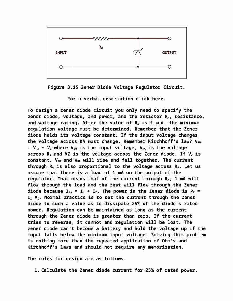
For a verbal description click here.
The equivalent circuit of a source-follower is shown in Figure 4.31. Summing the voltages around the outside loop we Have
Vin = vgs + vo (4.21) In a source-follower the value of RL is usually much less than rd so we can neglect rd in the following equation. The output voltage is given by
Vo = vgs Gm RL (4.22) Solving equations 4.21 and 4.22 for vgs and setting them equal gives
Vin - vo = vo / (Gm RL (4.23) ) Solving for vo / vin and remembering that AV is defined as vo / vin we have.
AV = Gm RL / (Gm RL (4.24) + 1) As with the emitter-follower, the output impedance of the source-follower can be obtained by shorting the input, connecting a generator V across the output and determining the current I which flows. The output resistance is V/I. The equivalent circuit is shown in Figure 4.32.
Figure 4.32 Finding Output Resistance of a Source-follower.
For a verbal description click here.
The current flowing through rd will be neglected. The current supplied by the generator is, I = Gm vgs (4.25)
Because the input is short circuited vgs = V and so, RO = V / I = 1 / Gm (4.26) .
The output resistance of a source-follower circuit is the parallel combination of the results of equation 4.26 and the resistor in the source of the FET. Note that unlike the emitter-follower the generator resistance has no effect on the output resistance.
Example 4.17.
In the circuit of Figure 4.30 the value of RS is 1 k ohm and the transconductance of the FET is 3000 micro mhos. What are (a) the voltage gain and (b) the output resistance of the circuit?
Solution:
(a) The gain is given by
AV = Gm RL / (Gm RL + 1)
AV = 3000 micro mhos x 1 k ohm / (3000 micro mhos x 1 k ohm + 1) = 0.75
(b) The output resistance is
RO = 1 / Gm = 1 / (3000 micro mhos) = 333 ohms.
The output resistance is 333 ohms in parallel with 1 k ohm which is 250 ohms.
You may be surprised by the low gain which is available from an FET source-follower. Designers seldom use a simple source-follower for just that reason. One very popular arrangement employs an N channel FET and a PNP BJT as shown in Figure 4.33. This circuit is often used as the input stage in oscilloscopes and AC voltmeters. This circuit is normally designed such that the collector current of the BJT is greater than the source current of the FET. This allows the BJT and the resistors to predominate in setting the operating point which eliminates the need for a trimming pot. Even so there is a DC offset between the input and output. The output may be anything from 1 to 4 volts more positive than the input. In DC coupled amplifiers such as those found in oscilloscopes this offset must be accounted for in some way to avoid adding it to the output.
Figure 4.33 Unity Gain Impedance Buffer Using an FET.
For a verbal description click here.
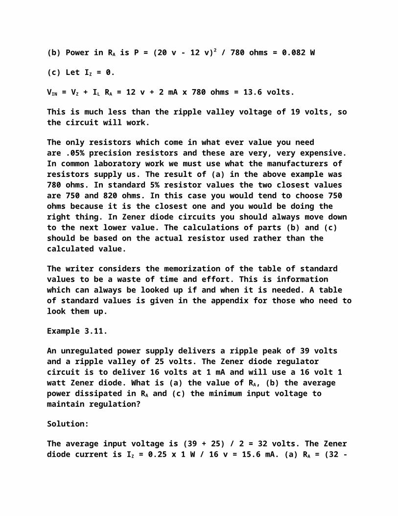
4.7 Differential Amplifier.
In the next chapter we will take up the study of operational amplifiers. A very important aspect of the op amp is its differential or difference input. A differential input consists of two input points with respect to ground. The circuit subtracts the two input signals. Thus the output of a differential amplifier is
VO = AV (V2 - V1 ) (4.37)
where AV is the voltage gain of the amplifier, V1 is the signal applied to the noninverting input and V2 is the signal applied to the inverting input.
The noninverting input is so named because an AC signal applied to this input is not inverted in phase. The inverting input is so named because an AC signal applied to this input is inverted in phase.
Figure 4.34 BJT Differential Amplifier.
For a verbal description click here.
Figure 4.34 shows a differential amplifier using BJTs. Q1 and Q2 work together to form the differential amplifier. Transistor Q3 along with R7, R8 and R9 form a constant current sink for the emitters of Q1 and Q2. The resistor network consisting of R7 and R8 keeps the voltage at the base of Q3 very stable regardless of changes in the base current of Q3. A very stable base voltage means that the emitter current will also be very stable and the collector current will also be very stable. Q3 carries the sum of the emitter currents of Q1 and Q2. If the emitter current in Q1 changes by a certain amount I, the emitter current of Q2 must change by an amount equal in magnitude and opposite in sign -I. This helps to maintain equal amounts of gain for both inputs.
Resistors R5 and R6 introduce emitter degeneration in Q1 and Q2, which lowers and further equalizes the gains. In an amplifier of this type emitter degeneration is not a bad thing. The gain is set by the ratio of R3 to R5 rather than the parameters of the transistors. It should be noted that R3 = R4 and R5 = R6. If maximum gain is desired resistors R5 and R6 may be replaced by pieces of wire but Q1 and Q2 must be very closely matched (have identical parameters) if the gains from the two inputs are to be equal in magnitude.
The output may be taken in either one of two ways. Output 1 is taken between the collectors of Q1 and Q2 as shown. This is a differential or as it is sometimes called a push-pull output. It is suitable for driving another differential amplifier or a balanced transmission line. Some oscilloscopes employ differential amplifiers from beginning to end. The deflection plates of a CRT must be driven from a differential output for best performance.
Output 2 is taken between the collector of Q1 and ground. The input marked with a - sign is the inverting input. A positive-going signal applied to the base of Q1 will cause its collector current to increase. That increase will cause a larger voltage drop across R3 which will cause the voltage at the collector of Q1 to decrease. The input marked with a + sign is the noninverting input. A positive- going signal applied to the base of Q2 will cause the collector current of Q2 to increase. That increase in collector current of Q2 must be mirrored by a decrease in the collector current of Q1. A decrease in the collector current of Q1 will cause the drop across R3 to decrease. The decreased voltage drop across R3 will increase the voltage at the collector of Q1. In case you forgot, we started with an increase in the input voltage which shows that the input marked with a + sign is the noninverting input.
Figure 4.35 FET Differential Amplifier.
For a verbal description click here.
Figure 4.35 shows a differential amplifier employing FETs instead of BJTs. You will note that Q3, R7, R8 and R9 have been replaced by a symbol which you may have never seen before. This is the symbol for a constant current sink. It is commonly used when showing internal schematic diagrams of integrated circuits. The FET differential amplifier functions in exactly the same way as the BJT differential amplifier except its input impedance is much higher. Because FETs are even harder to match than BJTs, R5 and R6 are still necessary. Indeed they may be chosen to bring the gain down close to unity in order to balance the gains of the two transistors. FETs are used to obtain high input impedance. When large amounts of gain are needed, BJTs will be found in the circuit. If both are needed in the same amplifier, you will find both FETs and BJTs in the circuit.
4.8 Problems.
1. The collector current of a BJT begins in the emitter, flows through the base region and ends up in the collector region. (This current refers to charge carrier current, not conventional current.) What kind of charge carriers (minority or majority)
make up the collector current when it is in the (a) emitter region, (b) the base region, and (c) the collector region?
2. In a PNP transistor the base current (conventional current) flows out at the base terminal. Where does it flow in?
3. In the circuit of Figure 4.3 the values are as follows: VCC = 28 volts, beta = 150, VINON
= 5 volts, VINOFF = 0 and RB = 8.2 k ohms. (a) If the lamp current is 65 mA, will the lamp be turned fully on? (b) After a few years the lamp burns out and someone replaces it with a lamp which draws 100 mA. Will this new lamp be fully turned on by the BJT switch? What will be the lamp current?
4. In the circuit of Figure 4.4 VINON = 10 volts and VINOFF = 2 volts. R1 = 3.3 k ohms and R2 = 820 ohms. All other circuit parameters are as shown in the figure. Is the switch on when the control signal is high and off when the control signal is low? Show detailed calculations for both off and on states.
5. For the starting conditions of problem 4, all of the students involved with designing and building the circuit have graduated. The transistor burns out and the equipment must be repaired because someone is giving a paper next week. Someone finds an old germanium transistor in a drawer and in desperation installs it in the circuit. The replacement has a beta of 100 but VBE to turn it on is 0.15 volts. Is the switch on when the control signal is high and off when the control signal is low? Show detailed calculations for both off and on states.
6. For the starting conditions of problem 4, all of the students involved with designing and building the circuit have graduated. The transistor burns out and the equipment must be repaired because someone is giving a paper next week. Someone finds an old transistor in a drawer and in desperation installs it in the circuit. The replacement transistor is a silicon unit but its beta is 25. Is the switch on when the control signal is high and off when the control signal is low? Show detailed calculations for both off and on states.
7. A transistor has the following parameters, hie = 2.5 k ohms and hfe = 85. If RL = 3.3 k ohms what is the gain of the common emitter amplifier?
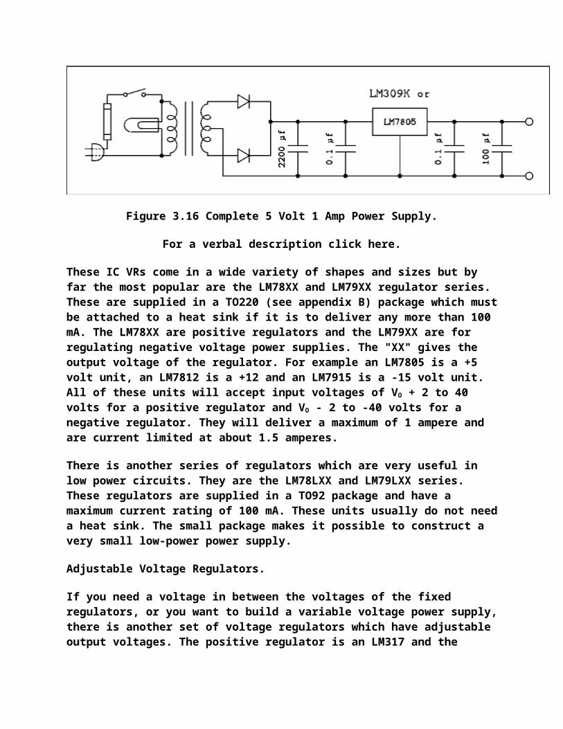
Figure 4.36 Common Emitter and Emitter-follower Amplifier.For Q1, hie = 2 k ohms and hfe = beta = 120.For Q2, hie 30 ohms and hfe = beta = 55.
For a verbal description click here.
8. Calculate the value of the collector current of Q1 in the circuit of Figure 4.36. Do not use an equation which is any more complicated than necessary.
9. Calculate the value of the collector current of Q2 in the circuit of Figure 4.36. Do not use an equation which is any more complicated than necessary.
10. Calculate the voltage gain of the emitter-follower stage in Figure 4.36. Remember to take everything into account when determining RL.
11. Calculate the voltage gain of the common emitter stage in Figure 4.36. Remember to take everything into account when determining RL.
12. The input resistance of a common emitter amplifier is equal to hie. What is the input resistance of the circuit of Figure 4.36?
13. In the circuit of Figure 4.36 if the 75 ohm load were removed, what would be the output resistance of the circuit?
14. What must the gate voltage be of an enhancement mode N channel MOSFET to (a) turn it on and (b) turn it off?
15. What must the gate voltage be of an enhancement mode P channel MOSFET to (a) turn it on and (b) turn it off?
16. Is it possible to make the circuit of Figure 4.23 work with depletion mode MOSFETs? Why or why not?
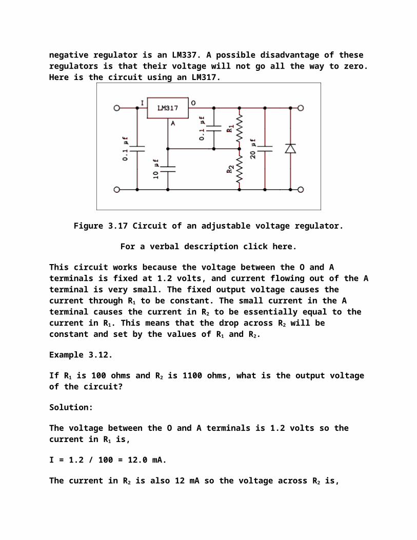
17. Is it possible to make the circuit of Figure 4.24 work with depletion mode MOSFETs? Why or why not?
18. A common source FET amplifier has a load resistance of 1.5 k ohms. The FET has a Gm of 3600 micro mhos and an rd of 200 k ohms. What are (a) the input resistance, (b) the voltage gain and (c) the output resistance?
19. An FET source-follower has a load resistor of 10 k ohms. The FET has a Gm of 2600 micro mhos and an rd of 200 k ohms. What are (a) the input resistance, (b) the voltage gain and (c) the output resistance including the 10 k ohm load resistor?
20. In the circuit of Figure 4.34 the collector current of Q3 is 1 mA. If the collector current of Q1 is 0.340 mA, what is the collector current of Q2?
21. In the circuit of Figure 4.35 if the drain current of Q1 increases by 50 microamps, what happens to the drain current of Q2?
22. If the gain of a differential amplifier is 10, V1 = +1.0 volt and V2 = +1.0 volt, what is the output voltage?
23. If the gain of a differential amplifier is 100, V1 = +1.00 volt and V2 = +1.01 volt, what is the output voltage? Be sure to give sign as well as magnitude.
24. If the gain of a differential amplifier is 100, V1 = +1.01 volt and V2 = +1.00 volt, what is the output voltage? Be sure to give sign as well as magnitude.
25. If the gain of a differential amplifier is 100, V1 = -1.00 volt and V2 = -1.01 volt, what is the output voltage? Be sure to give sign as well as magnitude.
26. If the gain of a differential amplifier is 100, V1 = -1.01 volt and V2 = -1.00 volt, what is the output voltage? Be sure to give sign as well as magnitude.
4.9 Answers to problems.
1. Part a, majority. Part b, minority. Part c, majority. 2. At the emitter. 3. Part a, required base current = 0.433 mA, supplied base current = 0.536. Lamp is
fully on. Part b, required base current = 0.667 mA. The lamp is not fully on. Lamp current = 80.4 mA.
4. On state. Required IB = 0.793 mA. Supplied IB = 2.12 mA. Switch is on. Off state. VBE
unloaded = 0.398 V. Switch is off. 5. On state. Required IB = 0.793 mA. Supplied IB = 2.80 mA. Off state. VBE unloaded =
0.398 V. BE is forward biased. Supplied IB = 0.378 mA. The switch will be between the on and off states.
6. On state. Required IB = 3.17 mA. Supplied IB = 2.12 mA. The switch is not fully on. Off state. Same as in problem 4.
7. AV = 112. 8. IC = 1.20 mA by equation 4.24. 9. IC = 47.2 mA by equation 4.23. 10. AV = 0.987. 11. AV = 43.6. Hint: There are 4 components that have to be added in parallel to make
up RL. 12. Rin = 1.57 k ohms. 13. RO = 16.4 ohms. 14. (a) Positive, (b) 0.
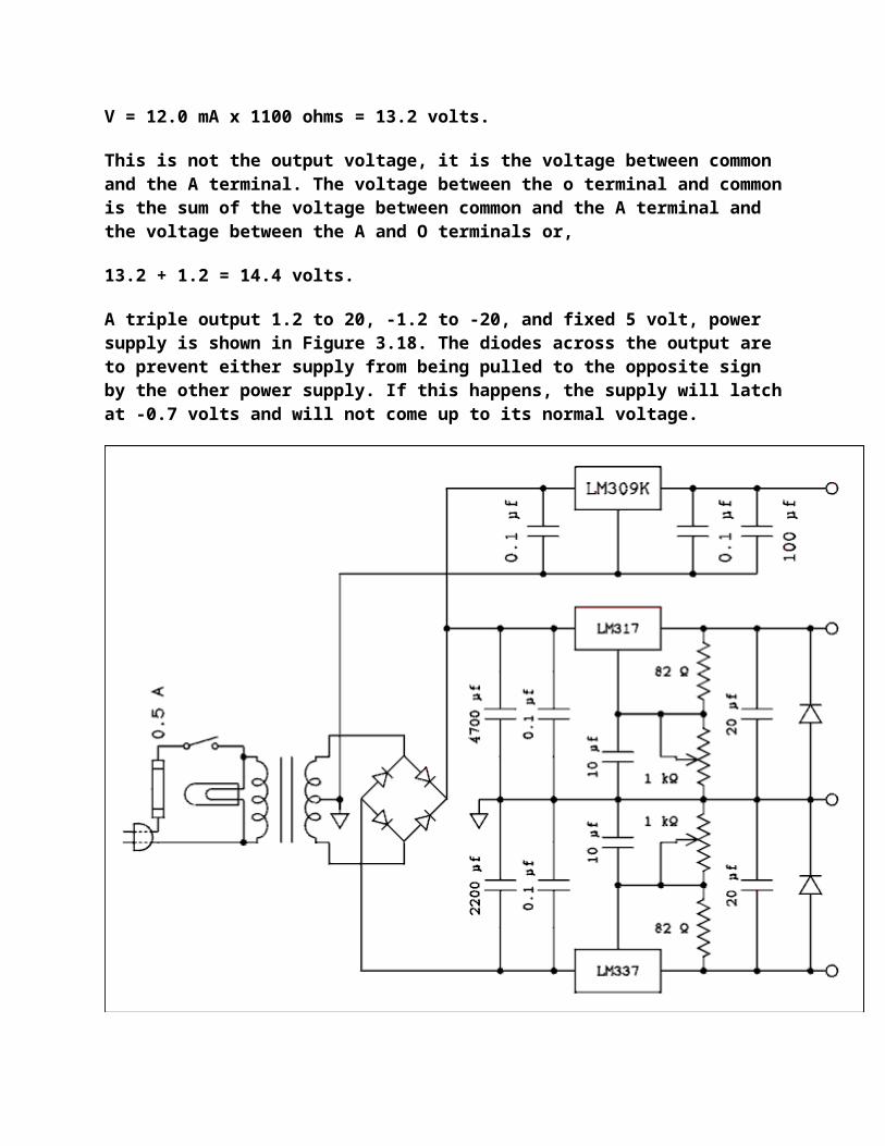
15. (a) Negative, (b) 0. 16. No. In the "on" state all is fine but in the off state one of the FETs will always be on. 17. No. Both FETs would be on, draw excessive current, and burn themselves out. 18. 1012 ohms, (b) -5.36, (c) 1.49 k ohms. 19. 1012 ohms, (b) 0.963, (c) 370 ohms. 20. ICQ2 = 0.660 mA. 21. The drain current of Q2 will decrease by 50 microamps. 22. VO = 0 V. 23. VO = + 1.00 V. 24. VO = - 1.00 V. 25. VO = - 1.00 V. 26. VO = + 1.00 V.
This page copyright © Max Robinson. All rights reserved.
Triode Vacuum Tubes. Chapter 4A
The Triode (3 Element) Vacuum 4A.1 Tube. Triode Amplifier Graphical Analysis, 4A.2 Load Line. Triode Amplifier Small Signal 4A.3 Analysis. Resistance Coupled Amplifier 4A.4 Charts. The Miller Effect. 4A.5 Cathode Follower. 4A.6 4A.7 Grounded Grid Amplifier. Cascode 4A.8 Amplifier. Problems. 4A.94A.10 Answers to Problems.
Chapter 4A.Triode Vacuum Tubes.
This chapter was not a part of the original textbook. Throughout most of my teaching career I assumed that the vacuum tube was dead. Somehow it kept coming back and saying "the rumors of my death are greatly exaggerated." My department head would not have looked kindly on the inclusion of a chapter on tubes because they were considered by physicists to be obsolete technology and not worthy of being taught in a modern physics department.
After retiring I decided to put up a web site devoted to tube technology and see how much attention it would attract. I was amazed by the response. It seems that the venerable old gal
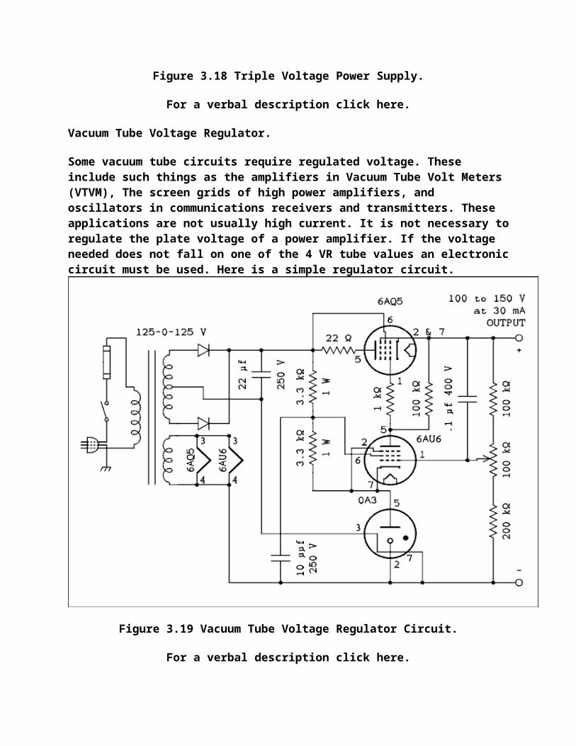
just won't roll over and die the way some would like her to do. She won't even play dead. Because this book is linked from both a tube and transistor site I need to put in a good chapter on tube theory and practice. So here it is.
4A.1 The Triode (3 Element) Vacuum Tube.
The tri part of triode means 3. There are three elements in a triode, the cathode, grid, and plate or anode. The heater doesn't count since it doesn't take part in the operation, it just provides the heat.
history.
In the United States Lee De Forest is generally credited with inventing the triode. His claim is under considerable dispute particularly in the United Kingdom. Since I wasn't there I don't know what happened but I have my suspicions. Court records of a case of De Forest versus Armstrong make it clear that De Forest didn't really understand the operation of the tube. That doesn't prove that he didn't invent it, maybe he stumbled onto it by accident. Maybe he ripped off someone else. Even though it all happened barely 100 years ago the mists of history have already settled over the facts and likely we will never know. We have the three element tube even if we aren't quite sure who to thank for it.
How it is made.
Photographs of the early Audions show a big spherical bulb with a filament like that in Edison's light bulb. Next to the filament is a grid which looks like hardware cloth (a very course window screen) and a flat plate. Modern triodes are usually cylindrical in construction with the filament or heater/cathode at the center, the grid surrounding it and the plate surrounding all as shown in Figure 4A.1 below.
Figure 4A.1 (a) filament type triodeand (b) heater type triode.
For a verbal description click here.
In these cylindrical tubes the grid takes the form of a helix, like a cork screw or spring. If you happen to have a 6AS7G or 6080WA in your tube collection you can see this construction. The plate instead of being continuous has an opening that runs the length of the cylinder and the shiny grid is clearly visible. There is a 9 pin miniature tube with the same construction but I don't know its number. I saw it once while looking for another tube and I didn't write it down.
How it works.
I've made that joke too many times already. Electrons are emitted from the cathode exactly the same as in a diode. They collect in a space charge around the cathode and protect it from heavy positive ions that could do serious damage. In normal operation the grid is made negative with respect to the cathode and never goes positive. (Except in radio transmitters). The grid does not attract electrons and because its wires are very thin, in modern tubes, few electrons run into it by accident. The electric field of the grid repels the negatively charged electrons and limits the number that can pass through to the plate. If the grid is made negative enough no electrons at all can get through. As the grid is made less negative it lets more and more electrons through. Figure 4A.2 below shows this by animation.
Figure 4A.2 Animation showing theoperation of a triode vacuum tube.
For a verbal description click here.
I know the animation is fascinating but do your best to tear yourself away from it and continue reading. Although the heater connections are not shown it is always assumed they are connected to the proper source of voltage for the heater. As the input signal swings positive the grid becomes less negative. This allows more electrons to get through to the plate which is an increase in plate current. The voltage drop across the plate resistor becomes greater and because the B+ end of the resistor is at a fixed voltage the plate end becomes less positive. You can see right off that as the grid voltage goes up the plate voltage goes down. This is the nature of this type of amplifier circuit. When the input signal swings negative the more negative grid cuts down the number of electrons getting through and the plate current is reduced. This causes the drop across the plate resistor to decrease and the
plate voltage gets closer to the B+ voltage, higher. Neither the grid voltage nor the plate voltage gets all the way to zero. If it should, the amount of distortion would be very high.
I have found in teaching amplifiers, common emitter as well as common cathode, that students often have trouble grasping the concept of increasing current resulting in decreased voltage. This in spite of demonstrations and laboratory experiments. Let's try using a bungee jumper as an analogy.
Figure 4A.3 Bungee Jumper Suspended From a Bridge.
For a verbal description click here.
This bungee jumper is in a slightly different situation than all other jumpers. There is an electric current flowing through the bungee cord. The greater the current, the longer the cord gets. As the current increases, the cord gets longer and the jumper gets closer to the ground. As the current decreases, the cord gets shorter and the jumper goes higher. So as the current goes up and down, the hapless jumper goes down and up. If he were to touch the ground or the bridge, his distortion level would be considerably increased.
Now remember that the current in a tube is in phase with the grid voltage. As the grid voltage moves up, so does the current. As the above analogy shows the plate voltage is out of phase with the plate current. And that is why a common cathode amplifier inverts the signal.
How it is Used.
Vacuum triodes are used primarily to amplify AC signals. To amplify means to make it bigger. The signals to be amplified are most likely to be in the audio range. Triodes are almost never used to amplify low power radio frequencies such as in a radio receiver. They are often found in high power radio transmitters, but that's another story.
An amplifier uses the principle shown in the animation above to increase the voltage of an AC signal. Although the voltmeters in the animation are shown deflecting by the same amount, the voltage in the plate circuit is actually much larger than the voltage in the grid circuit. This is what is meant by amplification.
The tube in the animation is biased by a battery in the grid circuit.*
* In the early days of tubes they were mainly used in radio receivers. Three different batteries were required to power up a radio. These were designated A, B, and C. The A battery lit up the filament, the B battery supplied the plates of the tubes with positive voltage and the C battery supplied the grids of the tubes with negative bias. While A is no longer used as a symbol for the filament or heater supply, (except in portable radios), the terms B and C are still very much with us as will be seen later in this chapter. Figure 4A.4 shows a schematic diagram of a common cathode triode amplifier.
Figure 4A.4 A cathode biased resistance coupled amplifier stage.
For a verbal description click here.
The circuit above is a practical amplifier stage. The B battery is not shown but it is replace by a connection symbol labeled Ebb. The C battery appears to be completely missing but instead of battery bias the tube uses what is often called self bias or cathode bias.
Cathode Bias.
Instead of the bias being supplied by an external battery it is developed in the cathode circuit of the tube or to think of it another way by the tube itself.
Let's assume that a tube needs the grid to be at -2 volts. That means that the cathode is at zero volts and the grid is at -2 volts. Now suppose we add 2 volts to both values. The grid voltage becomes 0 volts and the cathode voltage becomes +2 volts. The grid is still -2 volts away from the cathode which is required. Think about it. Let your left hand be the grid voltage and your right hand be the cathode voltage. Place your right hand even with the table top at the edge (zero inches) and your left hand 2 inches below your right (-2 inches). Your left hand is below your right hand. Now move both hands up 2 inches. Your left hand is now even with the top of the table (zero inches) and your right hand is 2 inches above it (+2 inches). Your left hand is still 2 inches below your right hand.
To place the cathode of a triode a small number of volts positive you place a resistor in the cathode circuit as shown in Figure 4A.4.
The notation used in this figure is consistent with the resistance coupled amplifier charts found in all tube manuals. Rc is the grid resistor, why not Rg? It's a throw back to the C battery which once supplied the grid bias in early radios. RK and CK are the cathode resistor and capacitor. Yes, they knew that cathode begins with a C but C was already used. Rb is the plate resistor, another throw back to the B battery. CC is the coupling capacitor and Rcf is the grid resistor of the following tube. The plate supply voltage is labeled Ebb. Why Ebb instead of B+? In formal electrical engineering writing the voltage on a tube element is notated as Eb for the plate and Ec for the grid. There is always a resistor between the supply voltage and the element. The supply voltage is distinguished from the voltage on the element by doubling the letter. For example, Ebb, and Ecc just the way it is done in transistors. Hmmm, wasn't it the other way around?
The positive voltage on the cathode is developed by the cathode current flowing through the cathode resistor. The tube, RK, and Rb constitute a simple series circuit. The grid does not take or give any appreciable current.
The capacitor in the cathode circuit is to keep the DC voltage constant. Without this cap the voltage can vary and reduce the gain of the amplifier. This gain reduction is accompanied by a reduction of distortion so in hi-fi circuits the cap is often omitted. More about this later.
Triode Characteristics and Parameters.
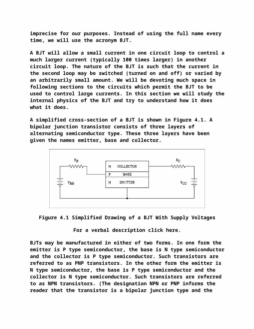
The behavior of tubes is described in two ways. One is by a graph of voltages versus currents and the other is by three numerical values called plate resistance, transconductance, and amplification factor. A graph of plate characteristics for a 6SL7 is shown in Figure 4A.5 below.
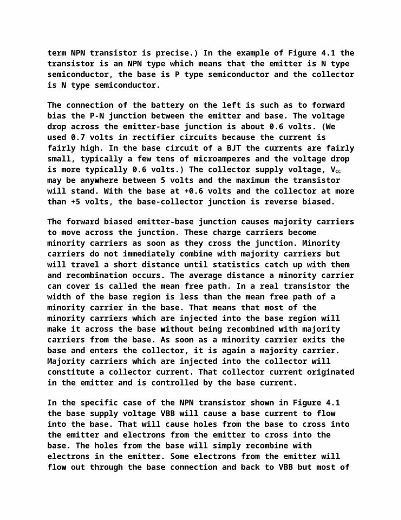
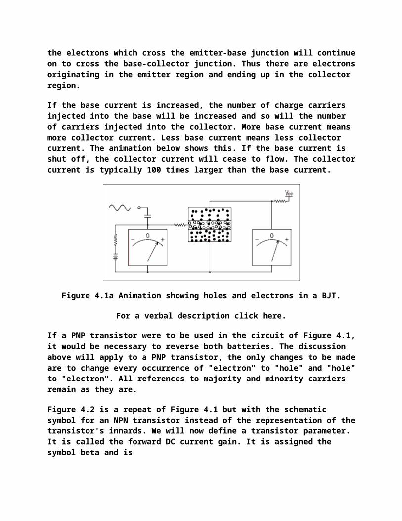
Figure 4A.5 Plate Characteristics of a 6SL7.
For a verbal description click here.
The horizontal axis is the voltage between the plate and cathode, not the voltage between the plate and ground. The vertical axis is plate current, and the number labeling each curve is the voltage between the grid and cathode. We will learn in the next section how to use this graph to design amplifiers and predict the behavior of existing amplifiers.
In section 4A.3 we will learn how to use the tube parameters to calculate gain without using the graph. Although we are about to pick parameter values off the graph these parameter values can be looked up in a tube manual. The purpose of picking them from the graph is to illustrate how they are defined.
Plate Resistance.
The plate resistance is NOT the resistor in the plate circuit of a tube. It is a parameter of the tube that is a voltage divided by a current which means its units are ohms. The plate resistance is symbolized by rp. The lower case r indicates that it isn't a real resistor. The plate resistance is defined as,
rp = change in Eb / change in Ibwith , Ec constant. (4A.1) Where Eb is the voltage between plate and cathode, Ib is the plate current, and Ec is the voltage between grid and cathode. In the graph above you take the change in plate voltage and current along one of the grid voltage lines. It is shown as being taken at two locations. At one place the voltage goes from 180 to 220 volts while the current goes from 2.33 mA to 3.25 mA. This works out to,
rp = (220 - 180 v) / (3.25 - 2.33 mA) = 43.5 k ohms. The other point is,
rp = (420 - 380 v) / (2.91 - 2.12 mA) = 50.6 k ohms. The tube manual states the parameters at a plate voltage of 200 volts and a current of 2.3 mA. Compare the results from the graph with the tube manual value of 44.0 k ohms. Not bad.
Amplification Factor.
The amplification factor is symbolized by the Greek letter μ and is defined as follows. μ = change in Eb / Ec with I b constant. (4A.2)
Where Eb is the voltage between plate and cathode, Ib is the plate current, and Ec is the voltage between grid and cathode. The amplification factor must be taken along a horizontal line which is constant current. The line must start on one grid voltage line and end on another one. The two values around 200 volts and 400 volts are,
μ = (131 - 271 v) / (0 - [-2] v) = -70.
μ = (328 - 400 v) / (-3 - [-4] v) = -72.
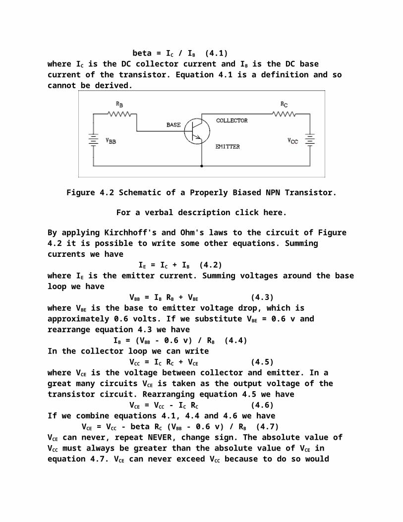
Although the tube manual never states μ as a negative number, it needs to be one for the calculations that will be performed in section 4A.3.
Transconductance.
The transconductance is redundant because, Gm = μ / rp (4A.3)
Where Gm is the transconductance usually given in micro mhos. Transconductance exists because the calculations on pentode tubes become easier when it is used instead of μ. The definition is,
Gm = change in Ib / change in Ec with Eb constant (4A.4) From the curves above the values are,
Gm = (4.61 - 2.8 mA) / (0 - [-1]) = 1,810 micro mhos.
Gm = (3.7 - 2.12 mA) / (-3 - [-4]) = 1,580 micro mhos.
The tube manual value is 1600 micro mhos. Calculating Gm from equation 4A.3 gives 1,609 and 1,423 micro mhos.
Parameter values are highly dependant on the operating point, plate voltage and current. If we had picked off values from lower down on the graph, say 0.5 mA, the parameters would have been quite far from the stated tube manual values. For use in calculations the most accurate parameter values can be obtained by picking them off the graph at the actual operating point.
4A.2 Triode Amplifier Graphical Analysis, Load Line.
Some find graphical analysis to be too tedious for their taste. However, if curves are available, it is the most accurate method of predicting the DC operating point and AC gain of a resistance coupled amplifier.* * The resistance coupled amplifier charts which we will cover in 4A.4 are much easier and just as accurate but they are restricted to one or two values of plate voltage and a few values of resistance. Graphical analysis can give accurate results over a wide range of plate supply voltages and load resistances.
The set of curves for the 6SL7 in figure 4A.6 show a complete graphical analysis. Resistance values were taken from the often mentioned resistance coupled amplifier charts to provide a standard of comparison. The data from the RCAC are tabulated along with the results of the graphical analysis at the end of this section.
If your screen is set to less than 1280 by 1024 this graph will overflow your screen. Most of the action is in the lower left corner so you shouldn't need to use your scroll bars very much.
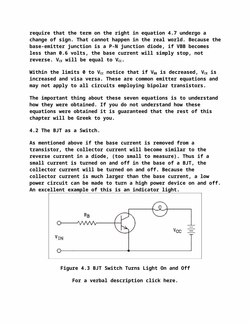
Figure 4A.6 Plate Characteristics with Graphical Solution.
For a verbal description click here.
DC Load Line.
Lower right end of DC load line = Ebb (4A.5)
Upper left end of DC load line = Ebb / Rb (4A.6)
We start with the value of load resistor and plate supply voltage. They are 100 k ohms and 250 volts respectively. The load line runs from zero current and full Ebb* and zero voltage and the current that would flow if the full value of Ebb was applied across the load. I = V / R = 250 / 100 k ohms = 2.5 mA. So we draw a line from 250 volts to 2.5 mA as shown by the red line in the figure.
Ignore the vertical red line and the magenta line that intersects with it. These are used in a later section.
With a 100 k ohm resistor in the plate circuit the tube can operate anywhere along the load line. For example, if we set the plate current to 1.5 mA the plate voltage, across the tube not the resistor, is 105 volts. If we set the plate current to 1 mA the voltage will be 153 volts. If we set the plate current to 0.5 mA the voltage will be 200 volts. If we were to use fixed bias on the tube we could operate it anywhere we wanted to on the load line but never off of it.
Bias Line.
If the tube is self biased, that is if a resistor is placed in the cathode, we would like to know where the tube will operate. We can do that by placing a bias line on the graph. Say we are using a 1.8 k ohm resistor in the cathode. If we placed 1 volt across the 1.8 k ohm resistor the current would be 0.555 mA. We mark this point on the -1 volt grid voltage curve. Now if we placed 2 volts across the 1.8 k ohm resistor the current would be 1.111 mA. We mark this point on the -2 volt grid voltage line and then connect the two points with a magenta line. Where the bias line crosses the load line is where the tube will operate. This is in remarkable agreement with the data from the RCAC. The operating point is often called the quiescent point or for short, the Q-point.
AC Load Line.
There is one more line on the graph to be explained. It is the green line which is an AC load line. The signal on the plate of the tube is of no use to us if we can't get it off and do something with it such as send it to the grid of another tube. That next tube will, and must, have a resistor from its grid to ground. A capacitor couples the signal from the plate of our tube to the next one. Assume the resistor in the grid of the next tube is 270 k ohms. The AC load on the tube is not 100 k ohms but the parallel combination of 100 k ohms and 270 k
ohms which is 72.97 k ohms. We must place another line on the graph that has a slope of 1/72,970. That can be a little tricky. We start by finding the lower right end of the line.
Lower right end of load line = EbQ + IbQ x AC Load (4A.7) Where EbQ is the Q-point plate voltage, IbQ is the Q-point current, and AC Load is the parallel combination of the plate resistor and the following stage's grid resistor. So the lower right end of the AC load line is,
L-R AC L-L = 157 v + 0.93 mA x 72.97 k ohms = 225 volts. Start the line at the bottom of the graph at 225 volts and make sure it passes through the point where the load line and bias line intersect. You only need to extend it as far as the zero grid voltage curve.
Voltage Gain.
The gain is the change in plate voltage divided by the change in grid voltage along the AC load line. The Q-point is between the -1 and -2 volt grid voltage lines so we might as well use these. At -1 volt the plate voltage is 130 volts. At -2 volts the plate voltage is 170 volts. The gain is (170 - 130) / (-2 - [-1]) = -40.
I did not precook this example. I did the numbers and let the chips fall where they may. I too am amazed at how close things came out. The RCAC data comes from laboratory measurements not graphical analysis.
There is no way to reliably evaluate distortion using the graphical method. It is possible to get a feel for it. Between Ec = 0 and -1 the plate voltage changes by 40 volts, between -1 and -2 40 volts, between -2 and -3 31 volts, and between -3 and -4 21 volts. We might be better off to operate the tube at higher current and lower voltage. We must not bias the grid so close to zero that it is driven positive. This will cause the operating point to shift on strong signals and there will be an audible recovery time after the peak.
Description Symbol ValueFromRCAC
ValueFrom
GraphicSolution
PlateSupplyVoltage
Ebb 250 Volts --
PlateLoad
Resistor Rb 100 k ohms --
FollowingStage Grid
Resistor Rcf 270 k ohms --
CathodeResistor Rk 1.8 k ohm --
PlateCurrent Ib 0.917 mA 0.93 mA
Grid BiasVoltage Ec -1.65 volts -1.68 volts
PlateVoltage Eb 158.3 volts 157 volts
VoltageGain AV 40.0 40
4A.3 Triode Amplifier Small Signal Analysis.
The small signal calculations are based on the small signal model of a vacuum tube. The triode small signal model is shown in Figure 4A.7 below.
Figure 4A.7 Small Signal Model of a Triode.
For a verbal description click here.
In science and engineering a model is something that represents a real system. It helps people working in the field to visualize the system more easily and make calculations based on the model that will predict the behavior of the real system. The triode tube with its resistors and power supply form a system and can be modeled.
As the figure above shows the model consists of a voltage source in series with a resistor. The resistor is symbolized with a lower case r because it is not a real resistor but a part of the model. The Greek letter μ stands for the amplification factor and rp for the plate resistance. These values can be looked up in a tube manual. If we combine the two parallel resistors Rb and Rcf into one and call it Rbc we can write some equations. The current in the circuit is,
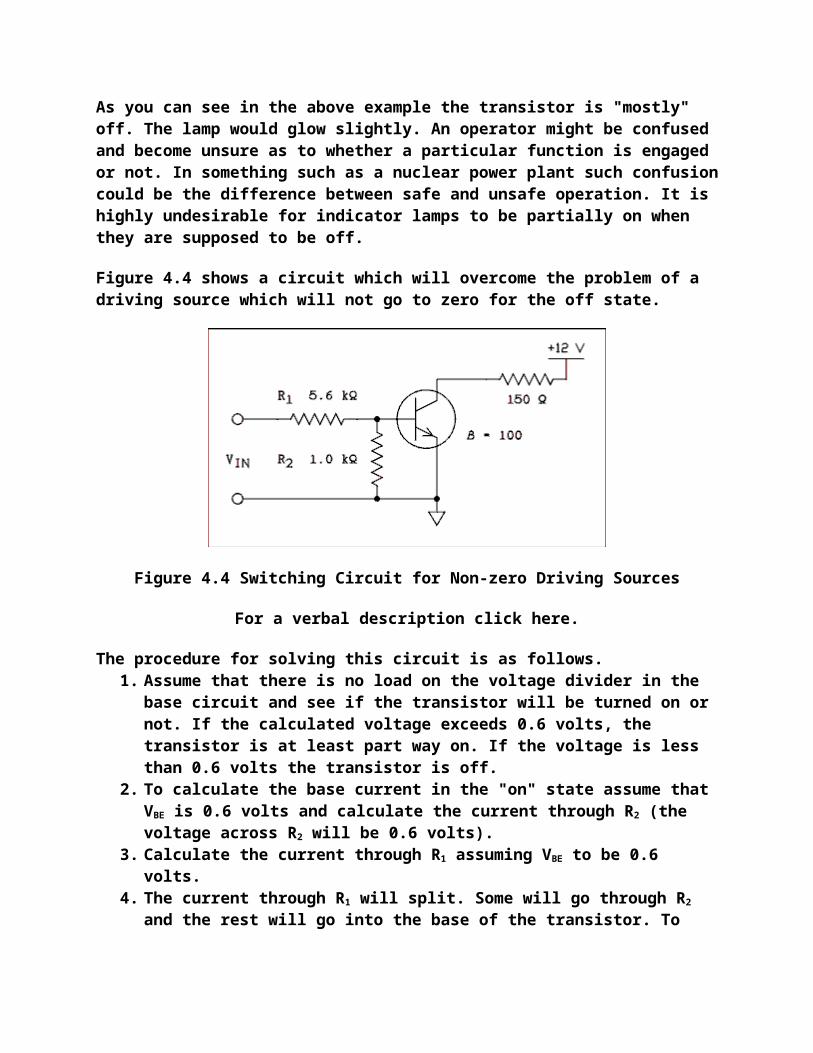
I = -μ Vgk / (rp + Rbc) The minus sign comes in because of the phase inversion of the amplifier. If the cathode is grounded then Vgk will be equal to Vin.
I = -μ Vin / (rp + Rbc) The output voltage is,
Vo = I Rbc Substituting I for I and dividing through by Vin gives,
VO / Vin = -μ Rbc / (Rbc + rp) Remembering that the gain AV = VO / Vin we have the voltage gain of a triode amplifier.
Av = -μ Rbc / (Rbc + rp ) (4A.8) Where Rbc is the parallel combination of Rb and Rcf as follows.
Rbc = Rb Rcf / (Rb + Rcf ) (4A.9)
Example 4A.1.
A 12AX7 has a plate load resistor, Rb, of 220 k ohms and the grid resistor of the following stage, Rcf, is 470 k ohms. Tube manual data on the 12AX7 gives Amplification factor = 100 and plate resistance = 80 k ohms. What is the gain of this 12AX7 amplifier
Solution:
First we calculate Rbc.
Rbc = Rb Rcf / (Rb + Rcf) = ( 220 k x 470 k ) / ( 220 k + 470 k ) = 150 k ohms.
Now we calculate the gain.
Av = -μ Rbc / ( rp + Rbc ) = -100 x 150 k / ( 80 k + 150 k ) = -65.2
Example 4A.2.
A triode tube is to be used as a single ended low power amplifier. The output transformer has a primary impedance of 5000 ohms. Think of Rb being 5 k ohms and Rcf as not present. Which of the following tubes will give the greatest voltage gain?
12AT7, Amplification Factor = 60, Plate Resistance = 1090012AU7, Amplification Factor = 17, Plate Resistance = 770012AV7, Amplification Factor = 41, Plate Resistance = 480012AX7, Amplification Factor = 100, Plate Resistance = 80000
Solution:
The gain for each is given by,
Av = -μ Rb / ( rp + Rb )
For the 12AT7 it is,
Av = 60 x 5000 / ( 10900 + 5000 ) = -18.9
For the 12AU7 Av = -6.69For the 12AV7 Av = -20.9for the 12AX7 Av = -5.88
The 12AV7 comes in first with -20.9 and the 12AT7 is runner-up at -18.9. Notice that the 12AX7 with its impressive amplification factor of 100 comes in last at -5.88. A high amplification factor may not guarantee a high gain amplifier.
Removing the Cathode Bypass Capacitor.
If the cathode bypass capacitor is left out of the circuit, as shown in Figure 4A.8 below, several things about the amplifier will change. The two most important are a reduction of gain and a reduction of distortion. The former is not good by itself but the latter is so good that it is worth the lost gain.
Figure 4A-8 A resistance coupled amplifierstage with unbypassed cathode resistor.
For a verbal description click here.
Figure 4A-9 Equivalent Circuit of Resistance CoupledAmplifier Stage with Unbypassed Cathode Resistor.
For a verbal description click here.
To derive the equation for the gain of the amplifier without a cathode bypass capacitor we must write loop equations around the loops in figure 4A.9.
We write the equation for the input loop up across the Vin generator, not shown, from G to K and back to ground across the cathode resistor.
Vin - Vgk + Ib Rk = 0 (4A.10.1) Then we write the loop equation around the output loop starting at the cathode, up across the generator, around the loop through rp, Rbc, and Rk, back to the cathode.
-μ Vgk - Ib rp - Ib Rbc - Ib Rk = 0 (4A.10.2) We want to eliminate Vgk between the two equations.
Vgk = Ib Rk + Vin (4A.10.3) Now we factor Ib out of the terms that contain only it.
-μ (Ib Rk + Vin) - Ib (rp + Rbc + Rk ) = 0 (4A.10.4) Now we multiply μ into the term on the left.
-μ Ib Rk - μ Vin - Ib (rp + Rbc + Rk ) = 0 (4A.10.5)
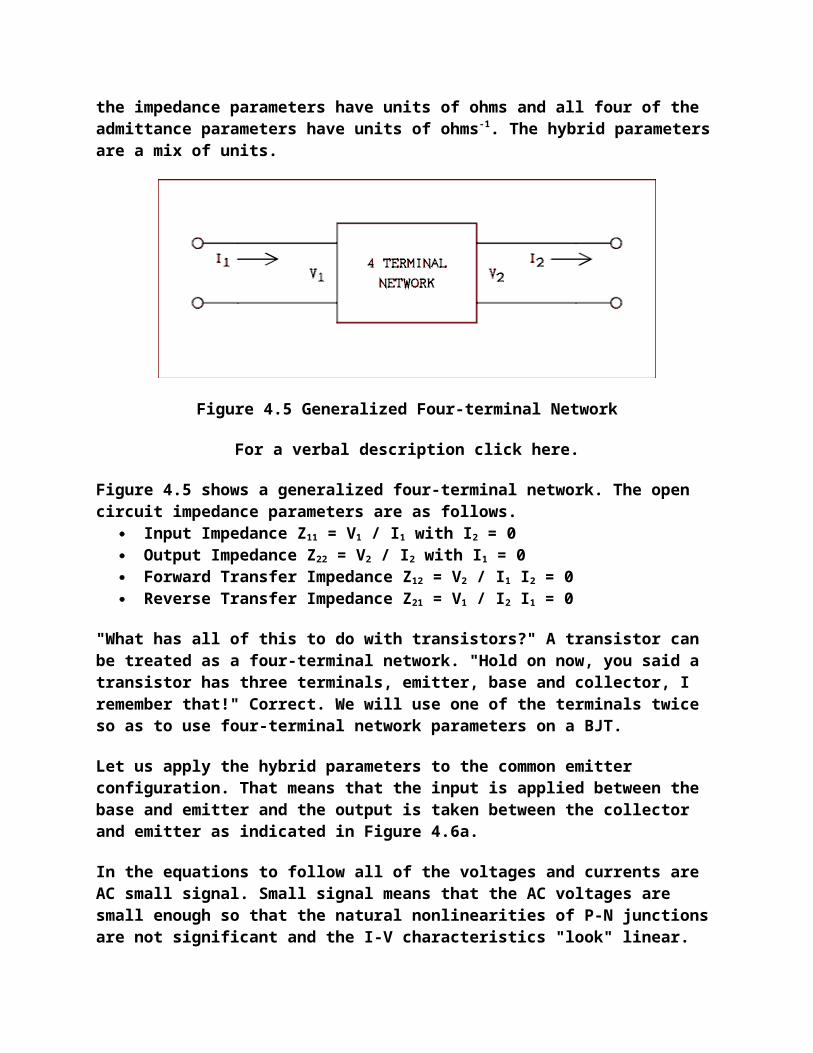
Now we put the term containing Ib inside the parentheses. -Ib (μ Rk + rp + Rbc + Rk) - μ Vin = 0 (4A.10.6)
Now we get Ib on the left side of the equation. -Ib (rp + Rbc + Rk + μ Rk) = μ Vin (4A.10.7)
Now we divide by the term that multiplies Ib and carry the minus sign over to the numerator.
Ib = -μ Vin / (rp + Rbc + Rk + μ Rk ) (4A.10.8) Now we can write Vo = Ib Rbc. We substitute (4A.10.8) into this equation. We also factor Rk out of the two terms in the denominator that contain it.
Vo = -μ Vin Rbc / (rp + Rbc + Rk [1 + μ]) (4A.10.9) Now we divide through by Vin and remember that AV = Vo / Vin.
Av = Vo / Vin = -μ Rbc / (rp + Rbc + Rk [μ + 1]) (4A.10.10) Where μ is the amplification factor of the tube, rp is the plate resistance Rk is the cathode resistor and Rbc is the parallel combination of Rb and Rcf.
Example 4A.3.
A 12AX7 which is without a cathode bypass capacitor has a plate load resistor, Rb, of 220 k ohms, a cathode resistor, Rk, of 3300 ohms, and the grid resistor of the following stage, Rcf, is 470 k ohms. Tube manual data on the 12AX7 gives Amplification factor = 100 and plate resistance = 80 k ohms. What is the gain of this 12AX7 amplifier
Solution:
Without a cathode bypass capacitor the gain is given by,
Av = μ Rbc / (rp + Rbc + Rk [μ + 1])
Remembering from Example 4A.1 the parallel combination of Rb and Rcf = 150 k ohms and substituting all values gives,
Av = 100 150 k / (80 k + 150 k + 3300 x 101 ) = 26.6
4A.4 Resistance Coupled Amplifier Charts.
Probably the easiest way to design a resistance coupled amplifier is to use the resistance coupled amplifier charts found in most tube manuals. If you don't have one you can pick one up on eBay. At any given time there are several for sail and they usually don't cost an arm and a leg. Don't go for one from the 20s, 30s, 40s, or even the 50s. They might leave you a few limbs short. Manuals from the 1960s are usually available and go for $10 to $30. The values found in these charts have been arrived at experimentally rather than by calculation. When it comes to tubes that's often the best way.
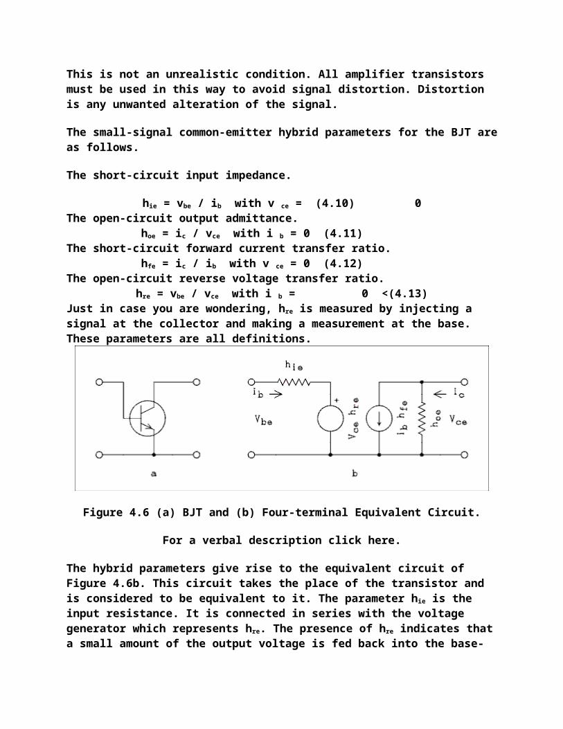
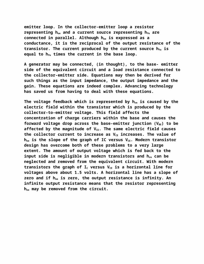
Figure 4A.10 Sample page from Sylvania Resistance Coupled Amplifier Chart.
No verbal description is available for this chart.
Yes, I do know how to rotate an image. When I tried reducing it to fit the width of a Windows 98 screen the text became unreadable. So I have kept it readable, big and turned on its side. Just turn your head to the left or download The image to your computer and rotate it yourself.
The only part that may need explaining is the zero bias section on the right.
Zero Bias.
An amplifier stage in which the cathode is grounded and there is no external source of bias is called a zero bias amplifier. The bias isn't really zero because the action of the tube will develop a small amount of bias. This is sometimes called contact bias because it is generated by electrons coming in contact with the grid.
The grid wires are thin and very few electrons strike them but there are billions of them passing by so even a small percentage is still a very large number. Electrons that strike the grid stick to it and give it a negative charge. If the grid resistor is made very large, say 10 meg ohms, the voltage on the grid will be almost a volt. Now, if the tube has been designed so this voltage is the optimum grid voltage, and some have been, the parts count of the amplifier stage can be reduced by two. A zero biased amplifier is shown in Figure 4A.11 below.
Figure 4A.11 A zero biased resistance coupled amplifier stage.
For a verbal description click here.
This circuit is most commonly used in All American 5 radios but is also seen in guitar amplifiers and hi-fi equipment. If the plate of a previous stage is coupled to a zero biased stage, as is often seen in magnetic phono preamps, a very low leakage capacitor must be used. A very tiny leakage in the capacitor would place a positive voltage on the grid. Even if there is nothing more than the wiper of a pot connected to the grid a DC blocking capacitor must be there to make sure that nothing upsets the bias voltage.
4A.5 The Miller Effect.
Anytime any where you have two conductors separated by an insulator you have capacitance. The plate and grid in a triode tube have capacitance between them. Because the tube inverts the signal the capacitance appears to be much bigger than it actually is. Lets explain it with resistors first. In Figure 4A.12a an AC generator is driving a single resistor. In Figure 4A.12b There is another generator in the circuit that always does the opposite of the one on the left but 50 times greater.
Figure 4A.12 Illustration of the Miller Effect.
For a verbal description click here.
Let us derive a general equation for this situation. Say that E2 = A E1. Summing the voltages around the loop gives.
E1 - I R - A E1 = 0 (4A.11.1) Solving this equation for E1 / I will give the effective resistance of the combination of the resistor and the second generator.
E1 / I = Reff = R / (1 - A) (4A.11.2) Where A is the factor that relates E2 to E1, R is the resistance of the resistor, and Reff is the effective resistance of R as seen by E1. In this particular case the value of A is -50. If we substitute R = 50 and A = -50 into (4A.11.2) we have,
Reff = 50 / 51 = 0.980 ohms.
If the generator at E1 is delivering 1 volt, the current through the resistor is I = 1 / 0.980 ohms = 1.02 amps. The 1 volt generator doesn't know about the 50 volt generator on the other end of the 50 ohm resistor. It doesn't know anything, it's just a stupid generator. All it knows is that when it puts out 1 volt it has to deliver 1.02 amps so it thinks it's driving a 0.98 ohm resistor. The second generator has made the resistor look 51 times smaller than it actually is. If a capacitor were to be substituted for the resistor its reactance would look 51 times smaller and since capacitance is inversely proportional to reactance the capacitor will look 51 times bigger.
The effective input capacitance of a triode amplifier is given by,
Cinp = Cin + Cgp (1 - Av) (4A.11.3) Where Cinp is the input capacitance of the amplifier, Cin is the tube manual value of input capacitance for the tube and Cgp is the given value of grid to plate capacitance. The value of Gain, A of the amplifier MUST be entered as a negative number. Notice that the factor (1 - A) switched from the denominator to the numerator. XC behaves the same as R but the capacitance is inversely proportional to XC. This causes the factor to be flipped.
Example 4A.4
In example 4A.1 we calculated the gain of a 12AX7 amplifier to be 65.2. The tube manual gives the input capacitance of the 12AX7 to be 1.6 pf and grid to plate as 1.7 pf. What is the effective input capacitance of this amplifier.
Solution.
Cinp = Cin + Cgp ( Av + 1 )
Cinp = 1.6 pf + 66.2 x 1.7 pf = 114 pf.
The Miller Effect is some what of a problem even at audio frequencies. The reactance of 114 pf at 10 kc is 140 k ohms. The effective output resistance of the 12AX7 amplifier we have been working with is the parallel combination of the tubes plate resistance, the plate resistor, and the following grid resistor. That works out to 52 k ohms. The upper 3 dB frequency is where Xc = R. If this tube stage were followed by an identical one the cutoff frequency would be f = 1 / (2 π R C ) = 1 / (2 π 52 k 114 pf ) = 26.8 kc. The response would be 1 dB down at approximately half of this frequency. The miller effect can become even more important at radio frequencies.
4A.6 Cathode Follower.
The cathode follower has a number of properties that make it useful in electronics. It can have an input resistance in excess of 10 Meg ohms and an input capacitance of less than 2 pf contributed by the tube. Wiring capacitance will likely be about 5 pf.
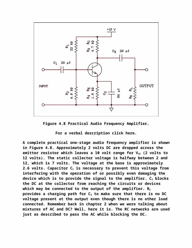
The output impedance may be as low as 100 ohms. This makes it very useful when a high resistance source needs to drive a low resistance load.
The cathode follower has a voltage gain of slightly less than unity but it does have current gain which means it qualifies as an amplifier because it increases the power of the input signal. A simple cathode follower is shown in Figure 4A.13.
Figure 4A.13 Simple Cathode Follower.
For a verbal description click here.
As the input voltage goes positive the plate current increases which increases the voltage drop across RK. Since the lower end of RK is at ground potential the upper end will get more positive. The cathode can't go up by the exact amount that the grid did. If it did, there would be no net change in voltage between cathode and grid to make the plate current increase. The cathode voltage changes by a little less then the change in grid voltage. It's called a cathode follower because where ever the grid goes the cathode follows along just a little behind.
Voltage Gain.
Figure 4A.14 shows the equivalent circuit using the triode model. DC voltages and coupling capacitors are not shown in models so the plate is shown as being grounded.
Figure 4A.14 Equivalent Circuit of a Cathode Follower.
For a verbal description click here.
As was done earlier, we will use this model to find the gain. First we write the loop equation around the input loop. As we did above we sum the voltage rises starting at ground, going up through the Vin generator, down from grid to cathode, and then back to ground through Rk.
Vin - Vgk + Ib Rk = 0 (4A.12) Then we start at the cathode and sum the voltages around the output loop.
-μ Vgk - Ib rp - Ib Rk = 0 (4A.13) Solving (4A.12) for Vgk gives,
Vgk = Ib Rk + Vin (4A.14) Substituting (4A.14 into (4A.13) gives,
-μ (Ib Rk + Vin) - Ib rp - Ib Rk = 0 (4A.15) Collecting terms and factoring out -Ib gives,
-Ib (μ Rk + Rk + rp) - μ Vin = 0 (4A.16) Summing the voltage drops in a counter clockwise direction around the VO and Rk loop gives,
Vo + Ib Rk = 0 (4A.17) Solving (4A.17) for -Ib gives,
-Ib = Vo / Rk (4A.18) Substituting (4A.18) into (4A.16) gives,
(μ Rk + Rk + rp) Vo / (Rk) - μ Vin = 0 (4A.19) Solving (4A.19) for Vo / Vin gives,
Vo / Vin = Av = (Rk μ) / (Rk[μ + 1] + rp ) (4A.20) If there was a load resistor, RL, connected across the output terminals in Figure 4A.13, The value of Rk to be used in equation 4A.20 would be the parallel combination of RK and RL.
Note the case of the K in Rk and RK. The lower case k indicates the AC load while the upper case K is reserved for the DC load.
Example 4A.5.
Calculate the gain of a cathode follower with AC loads of, (a) 100 k ohms, (b) 10 k ohms, and (c) 1 k ohm. The tube is a 12AX7 which has a plate resistance of 80 k ohms and an amplification factor of 100.
Solution:
We use equation 4A.20.
Av = (Rk μ) / (Rk[μ + 1] + rp)
(a). Av = (100 k ohms x 100) / (100 k ohms x 101 + 80 k ohms) = 0.982
(b>. 0.917
(c). 0.552
Example 4A.6.
Which one of the tubes listed below would give the best gain in a cathode follower where RK
is 1510 ohms and the load after the capacitor is 200 ohms?
6CG7/6SN7, Amplification Factor = 20, Plate Resistance = 7,700 ohms.12AT7, Amplification Factor = 60, Plate Resistance = 10,900 ohms.12AU7, Amplification Factor = 17, Plate Resistance = 7,700 ohms.12AV7, Amplification Factor = 41, Plate Resistance = 4,800 ohms.12AX7, Amplification Factor = 100, Plate Resistance = 80,000 ohms.
Solution:
Calculating Rk = 1510 x 200 / (1510 + 200) = 176.6 ohms.
6CG7/6SN7
Av = 176.6 x 20 / (176.6 x 21 + 7700 = 0.3096
12AT7, Av = 0.4889
12AU7, Av = 0.2760
12AV7, Av = 0.5926
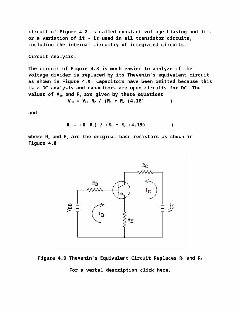
12AX7, Av = 0.1805
The 12AV7 gives the highest gain.
Output impedance.
In order to find the output impedance we replace the cathode resistor with a voltage generator as shown in Figure 4A.15. This could be done in the laboratory if it is done a little differently.
Figure 4A.15 Equivalent Circuit for Output Impedance.
For a verbal description click here.
Note that the input terminals have been shorted. We will now calculate the current Ib which results from the voltage generator V, and divide it into the voltage. Writing the equation around the input loop gives,
-Vgk - V = 0 (4A.21) The equation around the output loop is,
V - μ Vgk - Ib rp = 0 (4A.22) Solving (4A.21) for Vgk and substituting it into (4A.22) gives.
V + μ V - Ib rp = 0 (4A.23) Solving for V / Ib gives,
V / Ib = RO = rp / (μ + 1) (4A.25)
Example 4A.7.
Which of the 5 tubes listed below has the lowest output impedance?
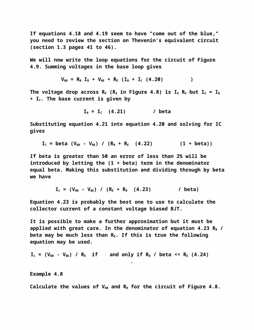
6CG7/6SN7, Amplification Factor = 20, Plate Resistance = 7,700 ohms.12AT7, Amplification Factor = 60, Plate Resistance = 10,900 ohms.12AU7, Amplification Factor = 17, Plate Resistance = 7,700 ohms.12AV7, Amplification Factor = 41, Plate Resistance = 4,800 ohms.12AX7, Amplification Factor = 100, Plate Resistance = 80,000 ohms.
Solution:
6CG7/6SN7 RO.
RO = rp / (&mu + 1) = 7700 / 21 = 366.7 ohms.
12AT7, RO = 178.7 ohms.
12AU7, RO = 427.8 ohms.
12AV7, RO = 114.3 ohms.
12AX7, RO = 792.1 ohms.
Looks like the 12AV7 wins again.
Operating Point.
Plate characteristic curves can be used to determine the Q-point of a cathode follower the same as for a common cathode amplifier. Because the plate connects directly to Ebb the load line goes straight up and down at the value of the voltage
Figure 4A.6 is repeated here so you won't have to scroll up to see it. This time look at the other set of lines.
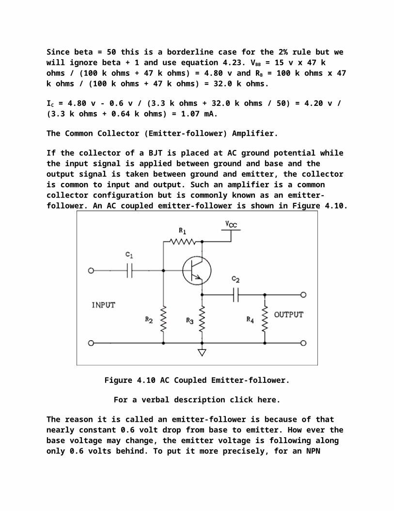
Figure 4A.16 Plate Characteristics with Graphical Solution.
For a verbal description click here.
The plate voltage is 300 volts so the load line is drawn vertically along that line. Let's assume a 1500 ohm resistor from the cathode to ground. 2 volts across 1500 ohms gives a current of 1.333 mA. We mark this point on the -2 volt curve. 3 volts across 1500 ohms gives 2 mA so we mark this point on the -3 line. We connect the points with a magenta line and the tube will operate where the magenta and red lines cross, 1.95 mA.
Taking the Cathode Resistor Into Account.
In example 4A.7 we calculated the effective output resistance at the cathode is if there were nothing else connected there. Obviously there is a resistor from the cathode to ground. This resistor is in parallel with the resistance presented by the tube. When calculating the output resistance of a cathode follower the cathode resistor may or may not be significant. Let's do an example where it is.
Example 4A.8.
For a 6SL7 calculate the (a) gain and (b) output resistance if a 1500 ohm resistor is used in the cathode. The amplification factor is 70, and the plate resistance is 44000 ohms.
Solution:
(a) Av = (Rk μ) / (Rk[μ + 1] + rp)
Av = 1500 x 70 / (1500 x 71 + 44000) = 0.698
(b) RO = rp / (μ + 1) = 44000 / 71 = 620 ohms.
We must now find the parallel combination of Ro with RK.
R = 620 x 1500 / (620 + 1500) = 439 ohms.
Practical Cathode Followers.
The circuit of Figure 4A.13 works but it can be of limited usefulness. The problem is its signal handling capability. The voltage at the cathode may be only one or two volts and the output voltage cannot go negative by anymore than this voltage. The voltage at the cathode can't go negative. This can be gotten around by using one of two circuits.
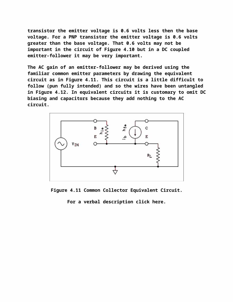
Figure 4A.17 Two Modified Cathode Follower Circuits.
For a verbal description click here.
The circuit in (a) might be preferred by some because it is a bit easier to design. However, it is rarely, if ever, seen. In fact, I have never seen it used in commercially produced equipment.
To design it, use the voltage divider equation to select the values of R1 and R2 to set the voltage at the grid. The cathode will be at most 3 volts higher. The value of the cathode resistor may then be calculated based on the desired cathode current. The voltage at the grid may be as high as half of Ebb.
Every tube has a maximum grid resistance stated in the tube manual. The parallel combination of R1 and R2 MUST NOT exceed this value.
Capacitor C1 is an absolute must because there is a DC level at the grid which must not be altered by anything that may be connected to the input.
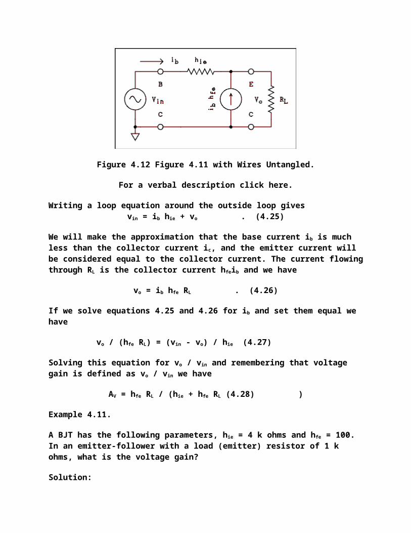
The circuit of (b) is standard and is known as the modified cathode follower. The two resistors in the cathode bias the grid positive and allow the cathode to be at a much higher potential to permit a larger voltage swing.
When a graphical solution is performed the value of RK1 is used to draw the bias line. The value of RK2 may be what ever is needed to drop the desired cathode voltage up to ½ of Ebb. When doing a graphical solution remember to subtract the voltage drop across RK2 from Ebb and use this number to place the vertical line on the graph. The horizontal axis is labeled "Plate Voltage" but it is actually the voltage between plate and cathode, not between plate and ground.
The major advantage of (b) over (a) is the increased input resistance. R1 has an effective resistance much larger than it actually is because the lower end is connected to a point that is at an AC potential that is in phase with the input signal and just a little smaller. If we assume the voltage at the junction of the three resistors is 0.9 of what is at the input, if the input voltage has a peak value of 1 volt the other end of the resistor has a peak value of 0.9 volts and the voltage drop across the resistor is 0.1 volts. That makes the effective resistance of R1 10 times the actual value of the resistor.
Example 4A.9.
A cathode follower uses a 12AX7 which has an amplification factor of 100 and a plate resistance of 80 k ohms. The resistor values are as follows. Rk1 = 10 k ohms, RK2 = 100 k ohms, and R1 = 470 k ohms. What are, (a) the voltage gain, (b) the output impedance, and (c) the input impedance.
Solution:
We must use the sum of RK1 and RK2 for Rk in equation 4A.20.
(a) AV = Rk μ / (Rk[μ + 1] + rp
AV = 110 k x 100 / (110 k x 101 + 80 k) = 0.983
(b) Output resistance of the tube alone is,
Ro = rp / (μ + 1) = 792 ohms.
The true output impedance is this value in parallel with 110 k ohms which is 786 ohms.
(c) We must use (4A.11.2) to calculate the value of Reff, the effective resistance of R1. The question is what value to use for A. We must use the gain between the input and the junction of the three resistors. This is,
A = Av RK2 / (RK1 + RK2) = 0.983 x 100 k / (10 k + 100 k) = 0.894.
The effective resistance of R1 is,
Reff = R1 / (1 - A) = 470 k / (1 - 0.894) = 4.43 Meg ohms.
A maximum grid circuit resistance could not be found for this tube but it is usually 2 Meg ohms for small signal triodes. This means that a maximum input impedance of 18.9 Meg ohms could be obtained with this circuit. Using this latter value a corner frequency of 1 cycle per second could be obtained with a capacitor of 0.00844 uf as C1.
4A.7 Grounded Grid Amplifier.
The first impulse would be to say that grounded grid amplifiers are never used in audio circuits. Nothing could be further from the truth. Negative feedback is often injected at the cathode of a stage making it a compound amplifier, both common cathode and grounded grid. Another use is in the long tail pair phase inverter where the signal from the cathode of the left hand tube drives the cathode of the right hand tube which really is in grounded grid mode.
The term "grounded" doesn't necessarily mean DC ground although that is the case in many radio frequency power amplifiers. In the next section we will see an RF amplifier in which the grid is at AC ground but a high positive potential. Here is the circuit of a simple resistance coupled grounded grid amplifier.
Many draftsmen will draw the tube with the plate on the right and the cathode on the left. The grid connection point is brought out the bottom and right to ground. I have shown the tube upright because that is the way you are accustomed to seeing it.
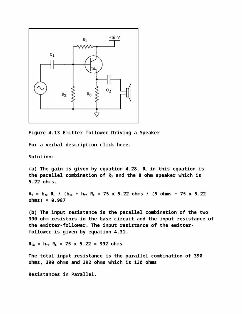
Figure 4A.18 Schematic of Grounded Grid Amplifier.
For a verbal description click here.
Driving the cathode is really no different than driving the grid. The most important difference is the input impedance. Instead of being an open circuit the cathode is a low impedance point as it is in a cathode follower. The other important difference is that the phase of the input signal is NOT inverted. Below is the equivalent circuit.
Figure 4A.19 Equivalent Circuit of Grounded Grid Amplifier.
For a verbal description click here.
Notice that the input signal is in series with the tube's voltage source. This is why FCC rules require that when computing the power of a grounded grid amplifier the power of the driver must be added to the power of the amplifier.
To derive the gain we write the loop equations as follows.
Vin + Vgk = 0 (4A.26)
Vin - μ Vgk - Ib rp - Ib Rb = 0 (4A.27)
Solving (4A.26) for Vgk and substituting into (4A.27) gives, Vin + μ Vin -Ib rp - Ib Rb = 0 (4A.28)
Now we write an equation for the output voltage. Ib Rb - Vo = 0 (4A.29)
Solving (4A.29) for Ib and substituting into (4A.28) gives, Vin (1 + μ) - (rp + Rb) Vo / Rb = 0 (4A.30)
Solving (4A.30) for Vo / Vin gives, Vo / Vin = Av = Rb (μ + 1) / (rp + Rb ) (4A.31)
The input impedance can be found by returning to equation (4A.28) and solving it for Vin / Ib.
Vin / Ib = Rin = (rp + Rb ) / (μ + 1) (4A.32)
Example 4A.10.
A grounded grid amplifier like that of Figure 4A.18 uses a 12AX7 and has an 1800 ohm resistor in the cathode and a 100 k ohm resistor in the plate. The parameters for the 12AX7 are, μ = 100, and rp = 80 k ohms. What are, (a) the voltage gain, and (b) the input impedance?
Solution:
(a) Calculating the voltage gain,
Av = Rb (μ + 1) / (rp + Rb)
Av = 100 k x 101 / (80 k + 100 k) = 56.1
(b) Rin = (rp + Rb) / (μ + 1) = 180 k / 101 = 1.78 k ohms.
The input impedance is this resistance, presented by the tube alone, in parallel with the cathode resistor.
Zo = Ro RK / (Ro + RK = 1.78 k x 1.8 k / (1.78 k + 1.8 k) = 895 ohms.
The grounded grid amplifier is not used in audio as a stand alone stage. As described above it is hidden in other stages. Where GG amps are found is in RF amplifiers. At radio frequencies the plate to grid capacitance of a triode is enough to cause it to oscillate. The capacitance feeds enough of the plate signal back to the grid to sustain oscillation. Obviously, this is undesirable in an amplifier. The grounded grid acts as an electrostatic shield between the input and output to prevent oscillation. In addition to that the cathode presents a low input impedance and it is not as susceptible to signals being induced as the high impedance grid.
4A.8 Cascode Amplifier.
The cascode amplifier is never used in audio circuits. I don't know why, maybe no one ever thought of doing it. It gives about as much gain as a pentode with about the same component count. I guess the idea of using two triodes for what would be one stage is just not appealing to audio amplifier designers.
The very first stage of a VHF TV receiver or FM receiver must amplify the small signal and add as little noise as possible. The emission and travel of electrons in the tube is a
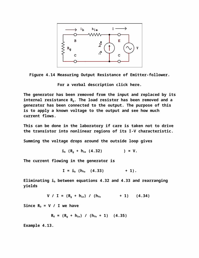
random process and randomness is noise. Pentodes give superior performance at RF because they have inherently higher gain and the screen grid acts as an electrostatic shield between the control grid and plate to keep down oscillation. But those two extra grids give the electrons more opportunities to run into something and produce more random noise. It would be real nice if we could have a tube as quiet as the triode, and with the gain and high input impedance of a pentode.
Enter stage left the cascode amplifier.
Figure 4A.20 Schematic of Cascode Amplifier.
For a verbal description click here.
This circuit is essentially a common cathode amplifier driving a grounded grid amplifier. The latter provides shielding of the input from the output. There is still some small RF voltage on the plate of the lower tube. There has to be or there wouldn't be any driving signal for the upper tube. The inductor is adjusted to bring the phase of the plate voltage to such a value as to reduce the miller effect in the lower triode to near zero.
Cascode amplifiers are constructed using duo triodes such as the 12AT7 which was designed for use in the tuners of early TV sets. The two sections are closely matched and they are in series for DC so the quiescent plate currents will be equal. The resistor network consisting of R1 and R2 is set so the voltages across each triode are equal. This means that μ1 = μ2 and rp1 = rp2.
Figure 4A.21 Equivalent Circuit of Cascode Amplifier.
For a verbal description click here.
We don't need to make any distinction between μ and rp for the two triodes. First we write the loop equation in the grid of the lower triode.
Vgk1 = Vin (4A.33) Now we start at ground and write the equation around the grid circuit of the upper triode.
-Vgk2 + μ Vgk1 + Ib rp = 0 (4A.34) Now we start at ground and write the equation around the main plate circuit loop. Because the two triodes are in series, Ib1 = Ib2 so there is no need to notate them separately.
-&mu Vgk1 - Ib rp - μ Vgk2g - Ib rp - Ib Rb = 0 (4A.35) Now we solve equation 4A.34 for Vgk2 and substitute into equation (4A.35)
Vgk2 = μ Vgk1 + Ib rp = 0 (4A.36)
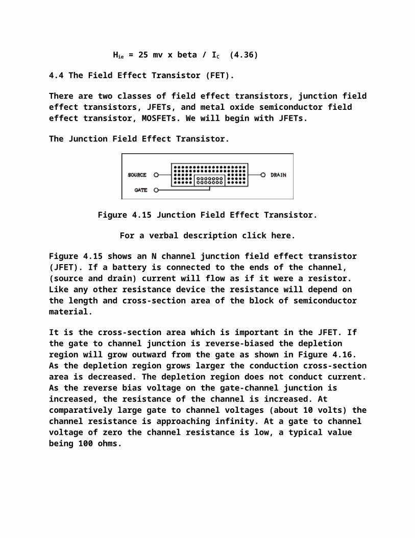
-mu Vgk1 - Ib rp - μ (mu Vgk1 + Ib rp) - Ib rp - Ib Rb = 0 (4A.37)
Substituting equation 4A.33 into equation 4A.37 gives -μ Vin - Ib rp -μ (μ Vin + Ib rp) - Ib rp - Ib Rb = 0
Now we multiply the parentheses through by μ, collect Ib terms and factor Ib out as a negative quantity.
-μ Vin - μ2 Vin -Ib (rp + μ rp + rp + Rb) = 0 Now we factor out -Vin and at the same time factor out rp inside the parentheses.
-Vin (μ + μ2) -Ib (rp [μ + 2] + Rb) = 0 Let's factor out μ so we don't have to deal with that μ2 term.
-Vin (μ [μ + 1]) -Vo / Rb (rp [μ + 2] + Rb ) = 0 (4A.39) To get the output voltage into the equation and eliminate Ib we write equation 4A.40 and substitute it into equation 4A.39.
Vo = Ib Rb
Ib = Vo / Rb (4A.40)
-Vin (μ [μ + 1]) = Vo / Rb (rp [μ + 2] + Rb ) (4A.41)
Now we divide through by -Vin, the parentheses on the right, and multiply by Rb. Vo / -Vin = Rb (μ [μ + 1]) / (rp [μ + 2] + Rb)
And finally we multiply through by -1 to obtain, Vo / Vin = Av = -Rb (μ [μ + 1]) / (rp [μ + 2] + Rb ) (4A.42)
The minus sign is because the amplifier inverts the signal and therefore the gain is a negative number.
Example 4A.11.
Calculate the gain of a resistance coupled cascode amplifier using a 12AX7 with a 220 k ohm plate resistor and a 470 k ohm resistor in the grid of the following stage. For the 12AX7, μ = 100, and rp = 80 k ohms.
Solution:
Referring back to Example 4A.1 the value of Rbc is 150 k ohms. This is the value to be used for Rb in equation 4A.42.
Av = -Rb (μ [μ + 1]) / (rp [μ + 2] + Rb)
Av = -150 k x 100 x 101 / (80 k x 102 + 150 k) = -182
Cascode Versus Pentode in Audio Service.
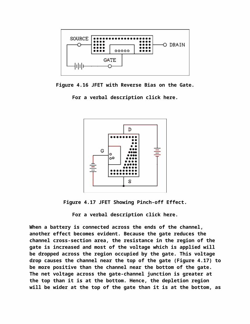
Figure 4A.22 Comparison of Cascode with Pentode Amplifier.
For a verbal description click here.
The figure shows a direct comparison between a cascode amplifier using a 12AX7 and a pentode amplifier using a 6AU6. The parts count is comparable. 1 tube and 3 capacitors for each. The cascode has one more resistor than the pentode but resistors are cheap. True it uses a higher Ebb voltage than the pentode but that could be corrected with a different design.
The pentode design was taken intact from the resistance coupled amplifier chart. The capacitors were computed for a 1 cycle per second corner frequency.
The design of the cascode began with the RCAC data. The 12AX7 data for Ebb = 250 volts and the plate and cathode resistors shown gives 128 volts as the quiescent plate voltage. Subtract the approximate 1 volt drop across the cathode resistor and we are real close to half of the Ebb across the tube and half across the plate resistor. With a cascode we make that 1/3 across each tube and 1/3 across the plate resistor and increase the Ebb to 375 volts.
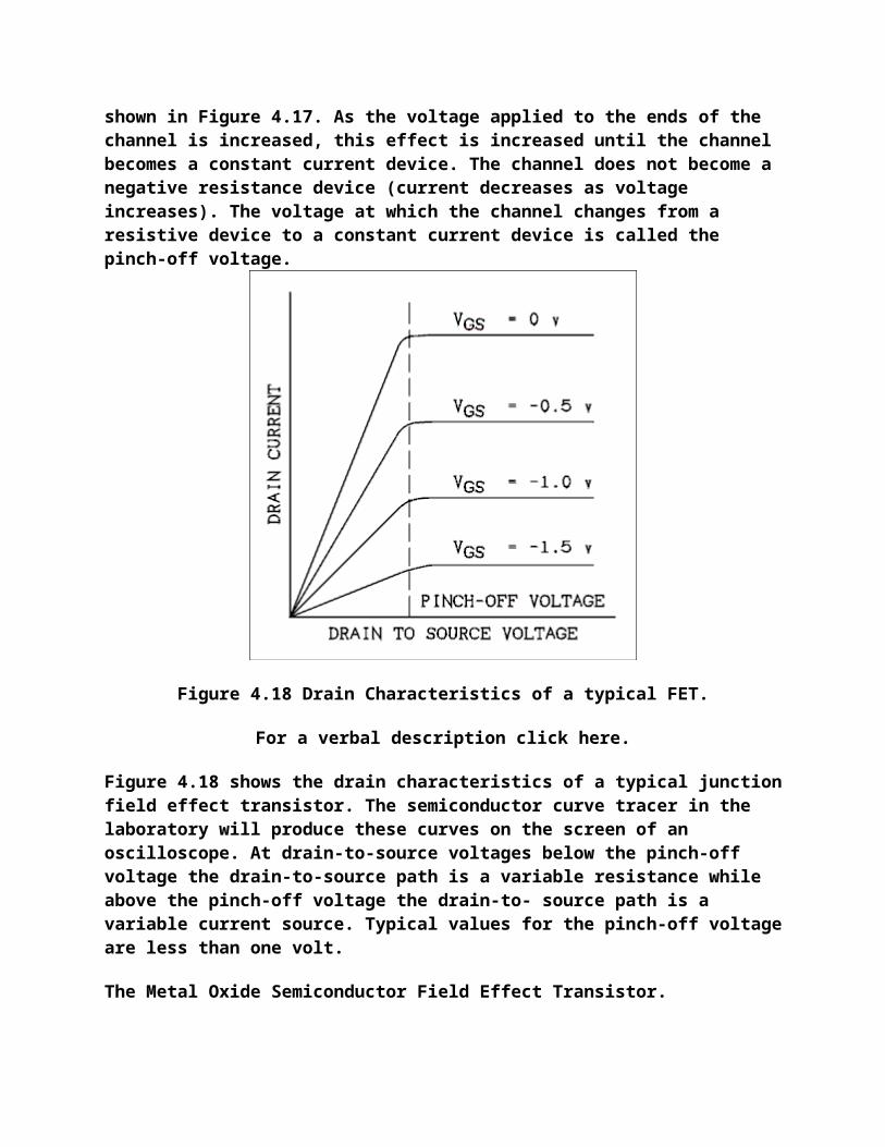
Then we calculate the voltage divider in the grid of the top triode to place 1/3 of the supply voltage on the grid. A similar design could be worked out for 250 volts using plate characteristics or a breadboard.
The difference between the gain of the pentode and the cascode only amounts to 1.6 dB. Distortion in the 6AU6 is, by the chart, 1.1% at 25 volts output. The cascode might be a viable solution when high gain and low noise are needed, provided you don't need a lot of output. The measured gain is 200 and here are the distortion figures.
Vo Distortion
25 8.3%
10 2.8%
2 0.56%
A cascode is not usable for a high gain high output amplifier. It should have lower noise than a pentode but I don't have time to build a fully shielded version of it to accurately measure the noise output. If one is working close to the noise floor obviously one is not going to be operating at a high level of output so in this application distortion should not be an issue. Noise shouldn't be an issue until the input voltage gets under 1 millivolt. At that level the output voltage would be 200 millivolts and the distortion would likely be unmeasurable.
4A.9 Problems.
1. Use the plate characteristics for the 6SL7 and (a) place a load line on the graph for a plate supply voltage of 400 volts and a resistor of 220 k ohms. (b) Place bias lines on the graph to determine the standard value cathode resistor to give a plate voltage as close as possible to 265 volts. (c) Place an AC load line on the graph for a following stage grid resistor of 470 k ohms. (d) Determine the gain from the AC load line. Note. You will need to print out the plate characteristics to have something to draw on. The best one to print may be Figure 4A.5 as what is drawn on it is all above 2 mA and will be out of your way.
2. A 12AU7 has a 100 k ohm resistor as a plate load. The following stage grid resistor is 470 k ohms. For a 12AU7 the amplification factor is 17 and plate resistance is 7700 ohms. What is the voltage gain of this stage?
3. A 6SN7 has a plate load of 47 k ohms and an unbypassed cathode resistor of 1 k ohm. There is no following stage grid resistor as this is in a Williamson amplifier phase inverter. The amplification factor is 20 and plate resistance is 7700 ohms. What is the voltage gain of this amplifier?
4. It is desired to have a 12AX7 amplifier with a gain as close to 10 as possible. The load resistance is 39 k ohms. Select a cathode resistor to give this gain. The parameters for the 12AX7 are, μ = 100, and rp = 80,000 ohms.
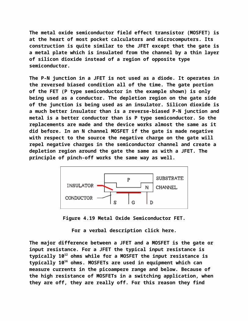
5. Design a 6SL7 amplifier from the sample page of a resistance coupled amplifier chart reproduced above. The only requirements are that Rcf must be 470 k ohms, the gain must be between 52 and 53, and the distortion must be less than 0.6%. In your answer state the values of, Ebb, Rb, Rk, (give 0 if zero bias is selected), Esig, Gain, and % Distortion.
6. A 12AT6 has a gain of 50. The plate to grid capacitance is 2.0 pf and the input capacitance is 2.2 pf. What is the total input capacitance of the amplifier?
7. A 6S4 is a 9 pin triode with a plate dissipation of 7.5 watts which is quite a lot for a small triode. Its amplification factor is 16 and its plate resistance is 3600 ohms. If this triode is used in a cathode follower where the total resistance in the cathode is 2500 ohms, what is (a) the voltage gain, and (b) the output impedance, including the cathode resistor?
8. A 6C4 is used as a grounded grid amplifier. The plate resistor is 47 k ohms, the cathode resistor is 1 k ohm, and the following stage grid resistor is 220 k ohms. The tube parameters are μ = 17, and rp = 7,700 ohms. What are (a) the voltage gain, and (b) the input impedance including the cathode resistor.
9. A 6SL7 is to be used in a cascode amplifier. The plate resistor is 220 k ohms and the following stage grid resistor is 470 k ohms. What is the gain? Tube parameters are, μ = 70, rp = 44,000 ohms.
4A.10 Answers to problems.
1. (a) The red line on the graph is the correct load line.
(b) There are two approaches to this problem. One is the estimation method and the other is the limits method. The estimation method goes this way. 265 volts is approximately half way between the -3 and -4 curves. So lets try -3.5 volts and see what happens. The current corresponding to 265 volts is about 0.62 mA. The trial Rk is then,
Rk = 3.5 v / 0.62 ma = 5,645 ohms.
The closest standard value is 5.6 k ohms. Then we check this with a bias line for 5.6 k ohms.
3 / 5.6 k = 0.536 mA4 / 5.6 k = 0.715 mA
We mark these values on the -3 and -4 grid voltage lines and connect them with a line. Where the bias line and the DC load line cross is the Q-point of the tube. It is always a good idea to check the adjacent values of 4.7 k and 6.8 k.
The limits method goes this way. The desired operating point is between -3 and -4 grid voltage. So we check the cathode resistor where the load line crosses these grid voltage lines.
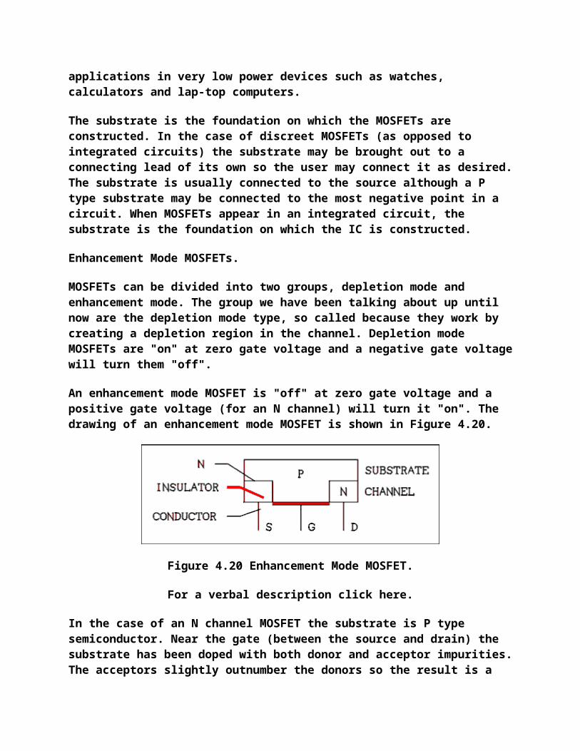
Rk-min = 3 v / 0.74 mA = 4054 ohms, andRk-max = 4 v / 0.51 mA = 7843 ohms.
There are 3 10% standard values between these limits. They are, 4.7 k, 5.6 k, and 6.8 k ohms. It is always a good idea to try all three just to be sure. The correct resistor is 5.6 k ohms.
(c) As has been worked in an example, the parallel combination of 220 k ohms and 470 k ohms is 150 k ohms. The current where the DC load line crosses the bias line for 5.6 k ohms is 0.63 mA.
Lower right end of AC load line = EbQn + IbQ x AC load.Lower right end of AC load line = 264 v + 0.63 mA x 150 k ohms = 358 Volts.
Anchor the lower right end at 358 volts and rotate the line until it passes through the point where the DC load line and bias lines cross. Stretch it as far as you can and draw the line. Note. I did these lines on a computer screen. I had to have the image zoomed in pretty far to read the graph. The length of the AC load line was limited by the zoomed area of the graph.
(d) The gain along the AC load line for grid voltages from -3 to -4 volts is 47.
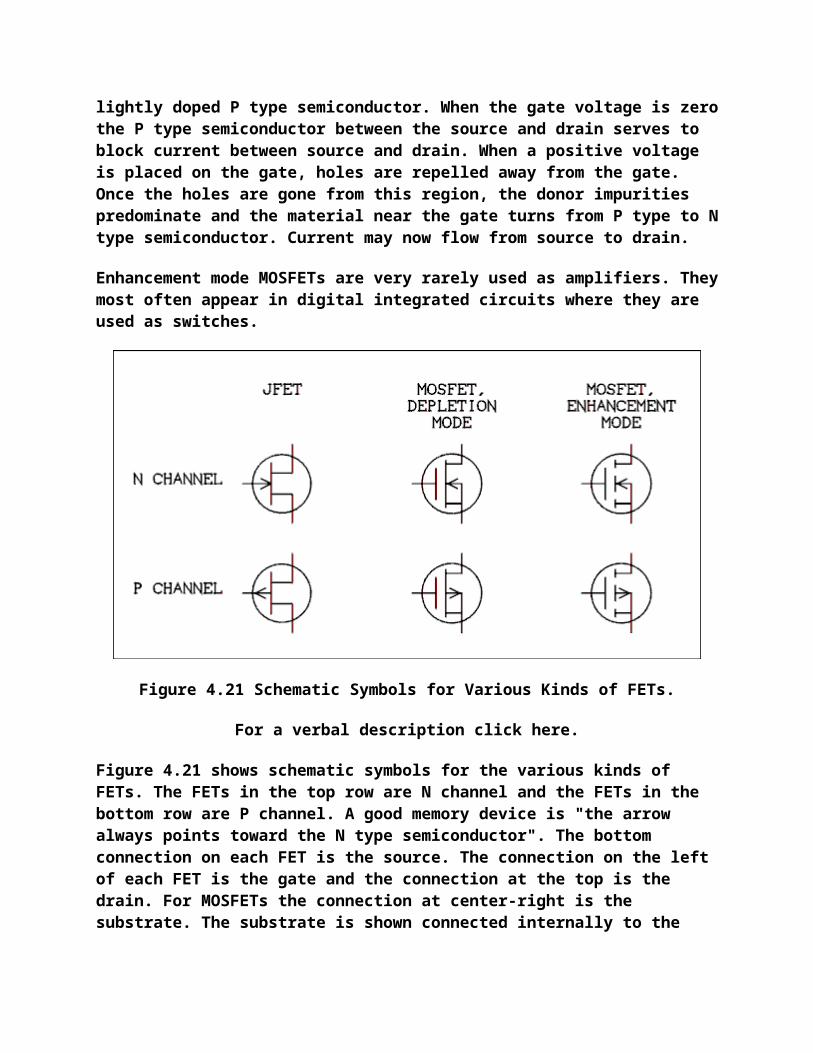
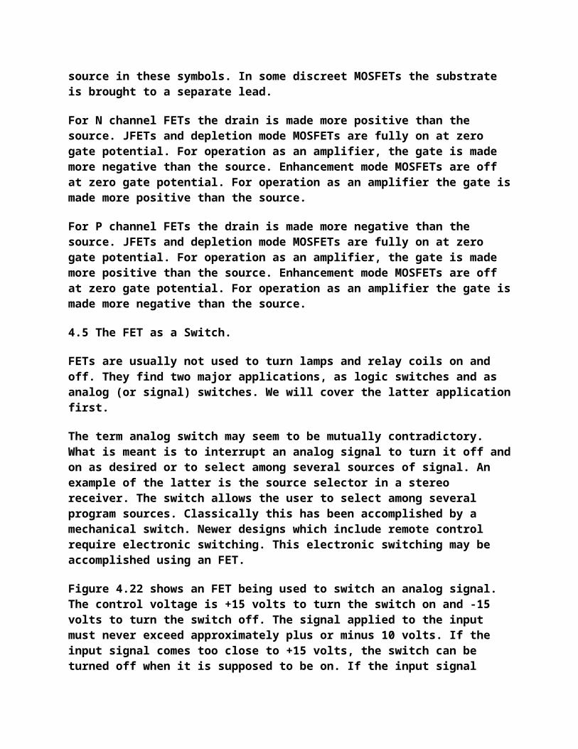
Figure 4A.23 Graphical solution to problem 1.
For a verbal description click here.
2. -15.5. 3. -12.4. 4. 2.7 k ohms. 5. There are two possible answers.
Self bias. Ebb = 250 V, Rb = 470 k ohms, Rk = 4.7 k ohms, Esig = 0.1 v, Gain = 52.5, and %Dist = 0.5.
Zero bias. Ebb = 250 V, Rb = 470 k ohms, Rk = 0, Esig = 0.1 v, Gain = 52.5, and %Dist = 0.4.
6. 104.2 pf 7. (a) 0.868, (b) 195 ohms. 8. (a) 15.0, (b) 721 ohms. 9. 262.
Multi Grid Tubes. Chapter 4B
Odes to Tetra and Penta. 4B.1 The Heptode, Pentagrid Converter. 4B.2 The Beam Deflection tube. 4B.3 Magic Eye and Cathode Ray Tubes. 4B.4 Oscillators. 4B.5 4B.6 Problems. Answers to 4B.7 Problems.
Chapter 4B.Multi Grid Tubes.
Development of the vacuum tube moved rapidly after the first triode was set loose on the world. The tetrode, pentode, and heptode had all been developed by 1930. Although they were considerably refined over the following 30 years the changes consisted mainly of the way in which they were packaged. The only significant development of which the writer is aware is the beam deflection tube which came out in the late 1950s, but we are getting ahead of ourselves.
4B.1 Odes to tetra and penta.
The triode was, and is, a pretty good tube but it does have a few problems. These problems were curable by inserting more grids into the tube. This gave rise to the Tetrode, 4 element tube, and the Pentode, 5 element tube.
Problems with the Triode.
The misbehavior of the Triode was attributed to the effect of plate to grid capacitance. There were two basic problems. These were 1) the miller effect and 2) oscillation. Due to the way a tube is constructed there is capacitance between the plate and grid. Because the tube inverts the signal the capacitance appears to be much bigger than it actually is. We studied the Miller effect in the previous chapter. If you don't remember that, it is suggested that you review section 4A.5.
Oscillation.
When triodes are used as radio frequency RF amplifiers all Hell breaks loose. The phase shifts that result from the use of tuned circuits in the grid and plate cause the signal fed back through the plate to grid capacitance to be positive feedback. That spells oscillator. If that's what you wanted then your delighted. But if you wanted to amplify small signals to make them bigger you would not be a happy camper.
There is such a thing as neutralization where in the circuit is arranged to feed signal back to the grid which is always opposite in phase and equal in amplitude to that fed back through the plate to grid capacitance. Neutralization is hard to adjust and increases circuit complexity. If there was only a way to reduce the plate to grid capacitance...
The Tetrode.
The logical thing to do seemed to be to place an additional grid between the control grid and plate. This grid could be placed at AC ground potential and would act as an electrostatic shield between plate and grid. Also the screen grid, as it was called, could be placed at a positive potential which would increase the gain of the tube by pulling more electrons toward the plate. However, a serious problem set in.
Secondary Emission.
When electrons strike the plate they are carrying a lot of kinetic energy. They give up that energy, in the form of heat, to the plate. The plate gets hot enough to begin emitting electrons. The impact of the incoming electrons helps to liberate others from the plate material. Think of them as being knocked loose. In a triode these secondary electrons have no place to go except back to the plate. It is the most positive thing in sight. In a pentode the screen grid is sitting there at a positive potential and because the plate voltage is going up and down with signal the screen grid may be, at that instant, more positive than the plate. The secondary electrons take off for the screen grid and ignore the plate. This takes
away from plate current and adds to screen current. Both things are bad. But even worse is the negative resistance effect. There is a point where an increase in plate voltage will give a decrease in plate current. If you try to work that one out with ohm's law you get a negative value for resistance. This phenomenon is shown in the oscilloscope photo below.
Figure 4B.1 Oscilloscope PhotoShowing Effect of Secondary Emission.
Scales, X = 20 V/cm, Y = 2 mA/cm.Grid voltage = 0.5 volts per step,
EC = 0 at the top. EC2 = 100 V.
For a verbal description click here.
Note the area where the line slopes slightly down to the right. This effect can be, and has been, used to make an oscillator but in an amplifier it leads to massive distortion. That's why there aren't any true tetrodes in your tube manual, unless you have a very old one. So if there aren't any true tetrodes, how did I get these curves. I used a modern tube and tied the suppressor grid to the plate. Just as tying the screen grid to the plate makes a triode, tying the suppressor grid to the plate makes a tetrode. Even with that, modern materials used in tubes don't allow very much secondary emission. The effect would be much more pronounced if an older tube were used. This was a 6AU6. The curves for a properly connected 6AU6 will be seen below. There were two basic solutions to the problem of secondary emission. One was to add yet another grid making a pentode, and the other was to cause the electrons to bunch up making a space charge that would repel secondary electrons back to the plate.
The beam Tetrode.
I can't say which came first historically speaking. Both solutions seem to have been around a long time. I have seen tubes such as the 6L6 called beam tetrodes in an old Tung-Sol manual I used to have. In looking through a 1937 RCA manual I find the 6L6 referred to as
a beam power amplifier although the diagram shows only two grids and two little angled lines between screen and plate but positioned on either side.
I did find a 22 which is called a "SCREEN-GRID RADIO-FREQUENCY AMPLIFIER". The specified screen voltage is less than 1/2 of the plate voltage. With the screen voltage set so low the excursions of plate voltage in an RF amplifier would not be large enough to take it into the secondary emission area.
The word "tetrode" must have already become a "4 letter word" among electrical engineers and had been banished from RCA literature by 1937.
Beam tetrodes operate by having the control grid and screen grid wires very accurately aligned. This minimizes electron collisions with the screen and causes the electrons leaving the screen to travel in thin beams. The plate is a little farther from the screen grid than it would otherwise be and there are two vertical pieces of metal that are internally connected to the cathode. These compress the electrons into a horizontal beam and form a concentration of negative charge that works to repel secondary electrons.
This structure can be clearly seen in a 6CB6. The grey rectangular plates are where the electrons impact. The silver colored pieces are the beam forming electrodes. The screen and plate are seen surrounding the cathode. The semicircular band is to support the two halves of the plate and connect them electrically. A picture I take can't do it justice. You need to hold one of these tubes in your hand and turn it at different angles to see how it is made. Although the tube manual calls this tube a pentode and the diagram shows a suppressor grid it is not brought out to its own pin as true suppressor grids are.
If you decide to break a tube and disassemble its innards, be careful. First of all, don't cut yourself on the broken glass. However there is a more subtle danger. Most of the materials used in tubes are rather toxic. I would urge you to handle them with gloves and when you are finished wrap them in several layers of aluminum foil before throwing them away. The contents of one tube thrown away isn't going to constitute a hazardous material spill but thousands would.
The True Pentode.
The pentode is constructed by inserting a third grid between the screen grid and plate. So now there are three grids in our tube. You may think it's getting a little crowded in there but just wait until we get to the heptode. The third grid is called the suppressor grid or usually just the suppressor. It is usually placed at the same potential as the cathode. In some tubes it is internally connected to the cathode although these may be beam tetrodes. The wires of the suppressor are widely spaced as compared to the control and screen grids so there is little effect on the high energy electrons coming from the cathode on their way to the plate. The secondary electrons are much lower energy and the suppressor is just enough to discourage them from going anywhere but back to the plate. In some special applications the suppressor grid may be used to control the gain of the amplifier tube. This can turn the pentode into a voltage controlled amplifier (VCA).
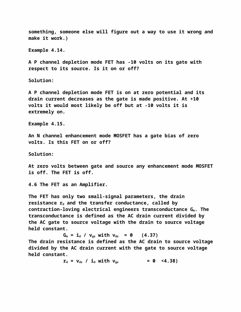
So there we have the modern pentode tube. High gain, small Miller Effect, and low likelihood of oscillating. As you might have guessed by the tetrode characteristics above the pentode characteristics are nothing like those of the triode. Figure 4B.2 shows the plate curves for a 6AU6 taken with a curve tracer and oscilloscope.
Figure 4B.2 Oscilloscope PhotoShowing Characteristic curves for a 6AU6.
Scales, X = 20 V/cm, Y = 2 mA/cm.Grid voltage = 0.5 volts per step,
EC = 0 at the top. EC2 = 100 V.
For a verbal description click here.
The tangle of lines at the left is an artifact of the curve tracer. If the plate voltage sweep is turned down they untangle and appear as they should. The almost horizontal lines mean that the plate resistance is very high and the best model for a pentode is a current source. Note that, unlike the tetrode, there is no change in the plate characteristics even when the plate voltage drops below the screen voltage.
Practical Circuit.
Like the triode the pentode can be connected as a resistance coupled amplifier. The tube manual circuit is shown below.
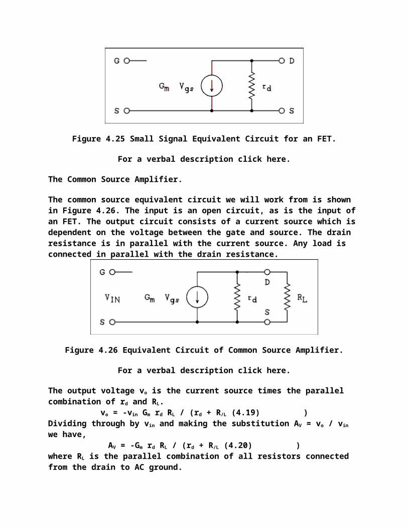
Figure 4B.3 A Pentode Resistance Coupled Amplifier Stage.
For a verbal description click here.
Once again the heater connections are assumed. The notation used here is consistent with the resistance coupled amplifier charts found in all tube manuals. You can design a pentode amplifier based on these charts, they will give you the gain and distortion at two values of input voltage.
In the next subsection you will see that small signal calculations are not accurate enough to be useful. However they can be used to correct the gain figures from the charts for an unbypassed cathode resistor.
Small Signal Calculations.
The equivalent circuit and calculations are quite different from the triode amplifier. The circuit is shown in Figure 3 below.
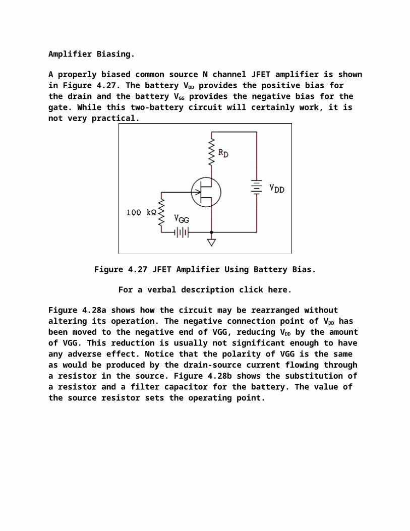
Figure 4B.4 The Small Signal Circuit of a Pentode.
For a verbal description click here.
When you look up a pentode in a tube manual you will find the transconductance rather than the amplification factor. If you are curious you can calculate it very simply. The amplification factor of a pentode may be found by,
μ = Gm rp (4B.1) Where μ is the amplification factor, Gm is the transconductance in mhos and rp is the plate resistance in ohms. The transconductance is always stated in micro mhos. The gain of a pentode amplifier may be calculated by,
Av = Gm rp Rbc / ( rp + Rbc ) (4B.2) Where Rbc is the parallel combination of Rb and Rcf as follows.
Rbc = Rb Rcf / (Rb + Rcf ) (4B.3) Where Gm is the transconductance of the tube, rp is the plate resistance, and Rbc is the parallel combination of Rb and Rcf as defined in equation 4B.3. The derivation of equation 4b.2 is so similar to that for the triode that it will not be given here.
One note of caution. The transconductance of a pentode is very sensitive to screen grid voltage. For example, for the 6AU6 the lowest value for transconductance is given for a screen voltage of 100 volts. Yet the resistance coupled amplifier charts give values of Eg2 of around 40 volts. Obviously the value of Gm needs to be scaled down accordingly. The tube manual gives a graph of transconductance versus grid number 1 voltage for values of grid number 2 voltage of 50, 100, and 150 volts for the 6AU6. An example will illustrate.
Example 4B.1
A 6AU6 has a stated transconductance of 3900 micro mhos and a plate resistance of 0.5 meg ohms. Calculate the gain for a plate resistor of 270 k ohms and a following stage grid resistor of 470 k ohms.
Solution:
First calculating the value of Rbc
Rbc = 270 k x 470 k / (270 k + 470 k) = 171 k ohms.
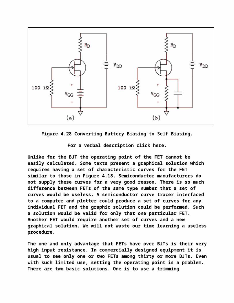
Av = Gm rp Rbc / (rp + Rbc)
Av = 3900 micro mhos x 500 k x 171 k / (500 k + 171 k) = 497
Here is the data from the resistance coupled amplifier chart for the 6AU6.
Ebb = 250 volts. Rb = 270 k ohms. Rc2 = 680 k ohms. Rcf = 470 k ohms. Rk = 1,000 ohms. Ic2 = 0.30 mA. Ib = 0.74 mA. Ec1 = -1.0 volt. Ec2 = 40 volts. Eb = 50 volts. Esig = 0.1 volt AC. Eout = 25 volts AC. Gain = 250. % Dist = 1.1 %. Esig(1) = 0.22 volts AC. Eout = 47.7 volts AC Gain = 217. % Dist = 2.6 %. (1) Taken at the point of 1/8 microamp of grid current. So which one is right? The chart of course. It was based on actual measurements performed in the laboratory.
We do have curves for the 6AU6 of transconductance versus grid 1 voltage for three values of screen grid voltage including 50 volts. 50 volts is close to 40 volts and we are given the grid 1 voltage. Looking at the graph we find the value of transconductance of 2200 micro mhos. Using this value in equation 4B.2 gives a gain of 280. We would rather have calculations that do better than that. The error is likely caused by the 10 volt difference in the screen grid voltage. We can do it another way as seen below.
Gain for an Unbypassed Cathode.
If the cathode bypass capacitor is left off the gain equation becomes. Av = Gm rp Rbc / [rp + Rbc + Rk (Gm rp + 1)] (4B.4)
Where Gm is the transconductance of the tube, rp is the plate resistance, Rk is the cathode resistor, and Rbc is the parallel combination of Rb and Rcf as defined in equation 4B.3. The derivation of equation 4b.4 is so similar to that for the triode that it will not be given here.
Resistance coupled amplifier charts don't give gain values for an amplifier with no cathode bypass capacitor. If you want to design a low distortion pentode amplifier and need to know the gain for an unbypassed cathode here is the procedure.
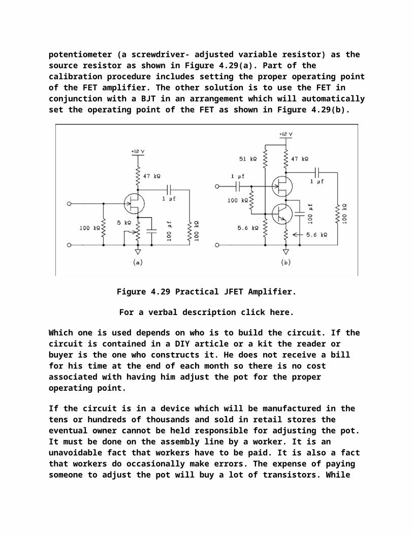
1. Design a pentode amplifier from the resistance coupled amplifier charts in a tube manual.
2. Use the stated value of low distortion gain in equation 4B.5 to find the operating value of Gm.
Gm = Av (rp + Rbc) / (rp Rbc ) (4B.5)
3. Use this value of Gm in equation 4B.4 to calculate the true gain.
Example 4B.2
The plate resistance of the 6AU6 is given as 0.5 meg ohms. The data from the resistance coupled amplifier chart is given above.
This is a lot more information than we need to work the problem but The real world never gives only the information we need and no more.
Calculate (a) the operating transconductance of the tube, (b) the gain without a cathode bypass capacitor.
Solution:
First we must calculate Rbc = Rb Rcf / ( Rb + Rcf ) = 270 k x 470k / (270 k + 470 k) = 171 k ohms. Now we calculate the operating transconductance.
Gm = Av (rp + Rbc) / (rp Rbc)
Gm = 250 (500 k + 171 k) / (500 k x 171 k) = 1962 micro mhos.
Now we calculate the gain without a cathode bypass capacitor as follows.
Av = Gm rp Rbc / [rp + Rbc + Rk ( Gm rp + 1)]
Av = 1962 micro mhos x 500 k x 171 k / [500 k + 171 k + 1000 (1962 micro mhos x 500 k + 1)]
Av = 101
When the circuit was breadboarded and tested the gain with the bypass capacitor in place came out as 225 rather than 250. With the cathode bypass capacitor removed the measured gain was 96. If Gm is corrected using a gain of 225, it comes out to 1766. The calculated gain of the unbypassed circuit is 97.1.
If the screen grid bypass capacitor is returned to ground rather than to the cathode, as shown in Figure 4B.5, The gain is much lower, 73.5 to be exact. Distortion and gain figures are summarized in the table below.
Figure 4B.5 Pentode Amplifier With No Cathode Bypass Capacitor.
For a verbal description click here.
CathodeResistorBypassed
ScreenGrid
BypassedTo
Vin Vout Gain Distortion
Yes Ground 0.1 v 22.5 v 225 3.8 %
Yes Ground 0.0425 V 9.6 v 226 0.72 %
No Cathode 0.24 v 22.5 v 93.8 1.8 %
No Cathode 0.1 v 9.6 v 96 0.35 %
No Ground 0.32 v 22.5 v 70 4.7 %
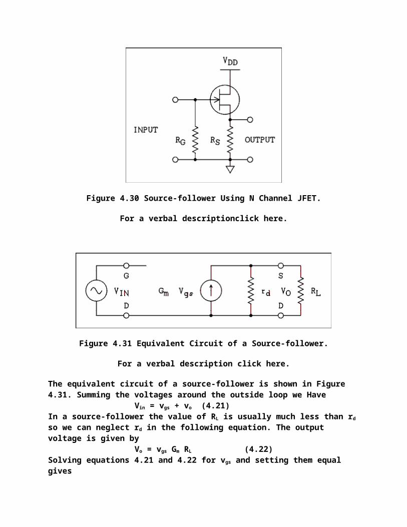
No Ground 0.1 v 7.35 v 73.5 0.32 %
4B.2 The Heptode.
Contrary to popular belief, the heptode was not invented by, or named by, a hepcat.
As the name implies the heptode has 7 elements, one cathode, 5 grids, and 1 plate. This tube is often called a pentagrid converter. Pentagrid as in 5 grids. It has one application, to serve as a mixer in radio receivers. (I have breadboarded and tested an audio voltage controlled amplifier using one of these tubes, but that's another story).
The Principle of Heterodyning
Heterodyning is more commonly known as "mixing", "conversion" or "modulation". OK; but what is it? If you combine two frequencies in a device known as a "mixer", "converter" or "modulator" you get two new frequencies. These new frequencies are the sum and difference of the two original frequencies. For example if you combine 5 MHz and 6 MHz in a mixer you get the two original frequencies and in addition you get 1 MHz and 11 MHz. If you combine 650 kHz and 1105 kHz you get 455 kHz, 650 kHz, 1105 kHz and 1755 kHz.
There are some types of mixers in which the original signals are canceled out and ONLY the sum and difference frequencies appear in the output. These devices are called "doubly balanced mixers" or DBMs for short. We will get to them shortly. But for now we will be talking about mixers in which the original two signals appear in the output along with the sum and difference frequencies.
So What is a Mixer?
Well, it's any nonlinear device. A nonlinear device is anything that has a graph that isn't a straight line. A diode, either vacuum or semiconductor makes an excellent mixer. A tube or transistor which is being driven into overload is another excellent mixer. The balanced variety consists of combinations of diodes and transformers, or transistors (usually in an integrated circuit). The beam deflection tube was developed in the 1960s that was a balanced mixer, but we're getting ahead of ourselves again.
The Superhet Receiver
The heptode was developed in the 1930s to combine the functions of oscillator and mixer into a single tube. Before that the two functions required two separate tubes. Reducing tube count also reduced cost so there was a great incentive to combine functions of two tubes into one.
We can not offer a full course in radio receiver design theory in this book. The interested reader is referred to other texts on the subject.
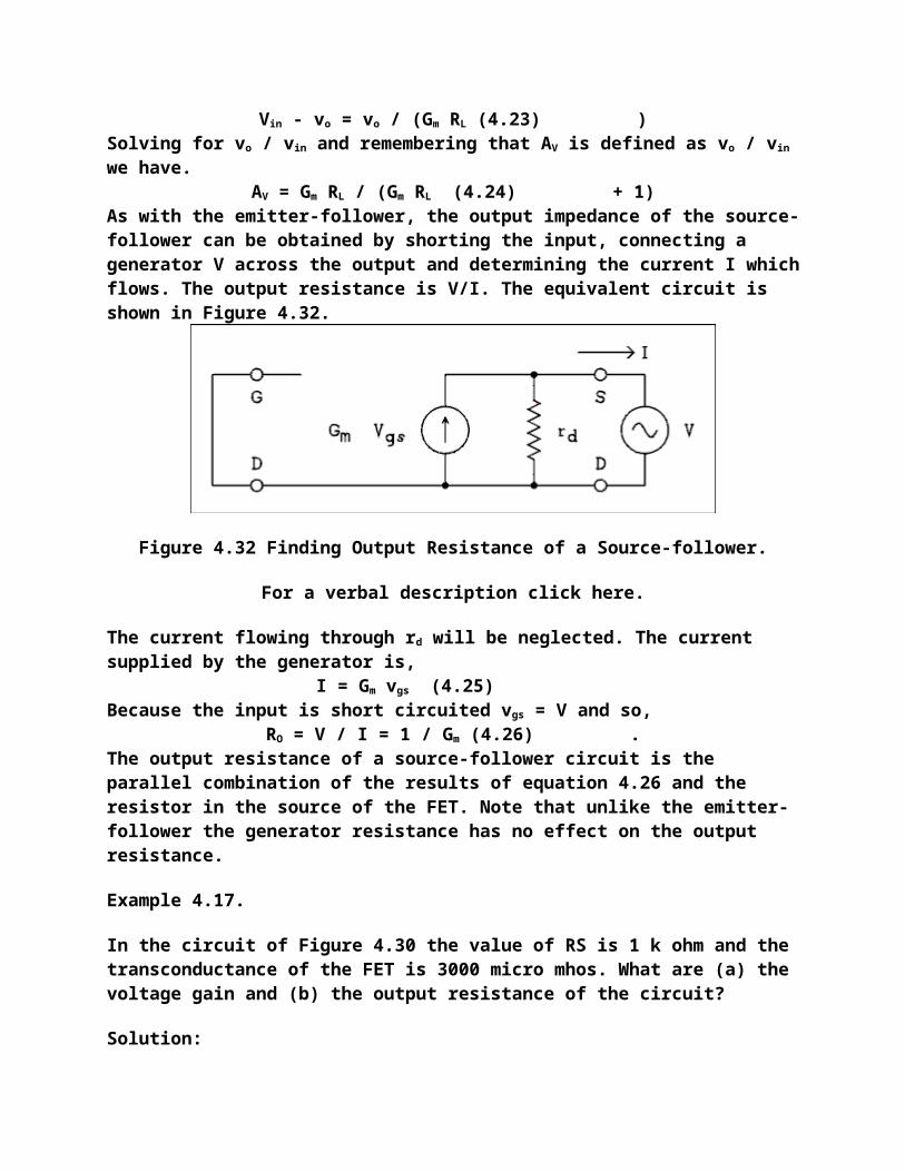
The block diagram of a single conversion super heterodyne receiver with an RF amplifier is shown in Figure 4B.6.
Figure 4B.6 Block Diagram of a Super Heterodyne Receiver.
For a verbal description click here.
I don't think there was ever such a thing as a heterodyne receiver. The word "super" appears to have been for marketing purposes but it is so ingrained into the consciousness of electrical engineers it will likely never be removed.
The RF Amplifier has a tuned circuit in its input and another in its output. It increases the level of the wanted incoming signal, reduces the level of the ones that are not wanted and helps to prevent the local oscillator from being radiated by the antenna. Such radiation could interfere with reception of other radio stations or services. Automatic gain control can be, and is, applied to the amplifying device here.
The converter contains an oscillator which is a locally generated signal that combines with the received frequency to generate the difference signal. The converter also does the job of mixing the local oscillator with the incoming signal. The tuned circuit of the oscillator is tuned along with the two tuned circuits in the RF Amplifier as the operator turns the tuning knob. The difference between the oscillator frequency and the incoming signal frequency is a constant. Therefore the converter delivers a constant frequency signal to the Intermediate Frequency Amplifier. Some AGC (Automatic Gain Control) is also applied to the mixer part of the converter.
The IF (intermediate Frequency) amplifier follows the converter. Its frequency is lower than the frequencies of the stations being received but higher than audio frequencies. Thus, the reasoning went, it is between the station frequencies and audio frequencies so it is intermediate. Its operating frequency is fixed and cannot be changed by the operator, or even by a skilled technician. This is where most of the selectivity of the receiver is found. Selectivity is the ability of a receiver to bring in a single station and cut out the stations that are nearby in frequency. More AGC is applied to the amplifying device in the IF amplifier.
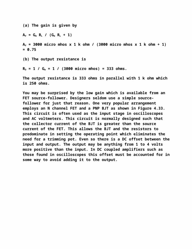
Following the IF amplifier is the detector. This is the combination of devices and circuitry that recovers the audio from the AM signal. The detector also recovers a negative DC voltage that is proportional to the strength of the incoming signal. This is the AGC (Automatic Gain Control) voltage that is applied to the IF and RF amplifiers and the converter.
If this is a stand alone radio or short wave receiver, the audio amplifier will deliver 1 or 2 watts of power to drive a speaker. If it is a high fidelity tuner The amplifier will deliver a line level signal at a moderate impedance level for driving the input circuitry of an amplifier.
Image Frequencies.
As mentioned above a mixer/converter produces the sum and difference frequencies of the two original input signals. The mixer can and does produce two difference frequencies. If we call the frequency of the oscillator fo a frequency below the oscillator f1 and a frequency above the oscillator f2, the difference frequency fd will consist of,
fd1 = fo - f1
fd2 = f2 - fo
Suppose you live in Cincinnati Ohio so you have a strong local station on 1530 kHz. (It used to be WCKY. I don't know if it has changed. Well, suppose you would like to listen to an out of town station which is operating on 620 kHz. You tune your local oscillator to 620 + 455 = 1075 kHz. What do you hear? Well, WCKY on 1530 is also there and combines with your local oscillator on 1075 to produce a difference frequency of 1530 - 1075 = 455 kHz. OOPS! That's the main drawback to a Superhet receiver. It receives two frequencies simultaneously at the same time. It's up to the two tuned circuits in the RF amplifier which are tuned to 620 kHz to reject the strong signal on 1530 so you can listen to the station you want to hear. Low cost AM radios omit the RF Amplifier stage which places only one tuned circuit between the antenna and converter. Such radios are not very good at rejecting the unwanted frequencies. They are called "image" frequencies by radio engineers.
The Tube and the Circuit.
Because the tube was developed to operate as a converter in AM and short wave receivers, it and the circuitry that make it work are inseparable. Figure 4B.7 is the converter section of an All American 5 radio that might have been sold between 1938 and 1950.
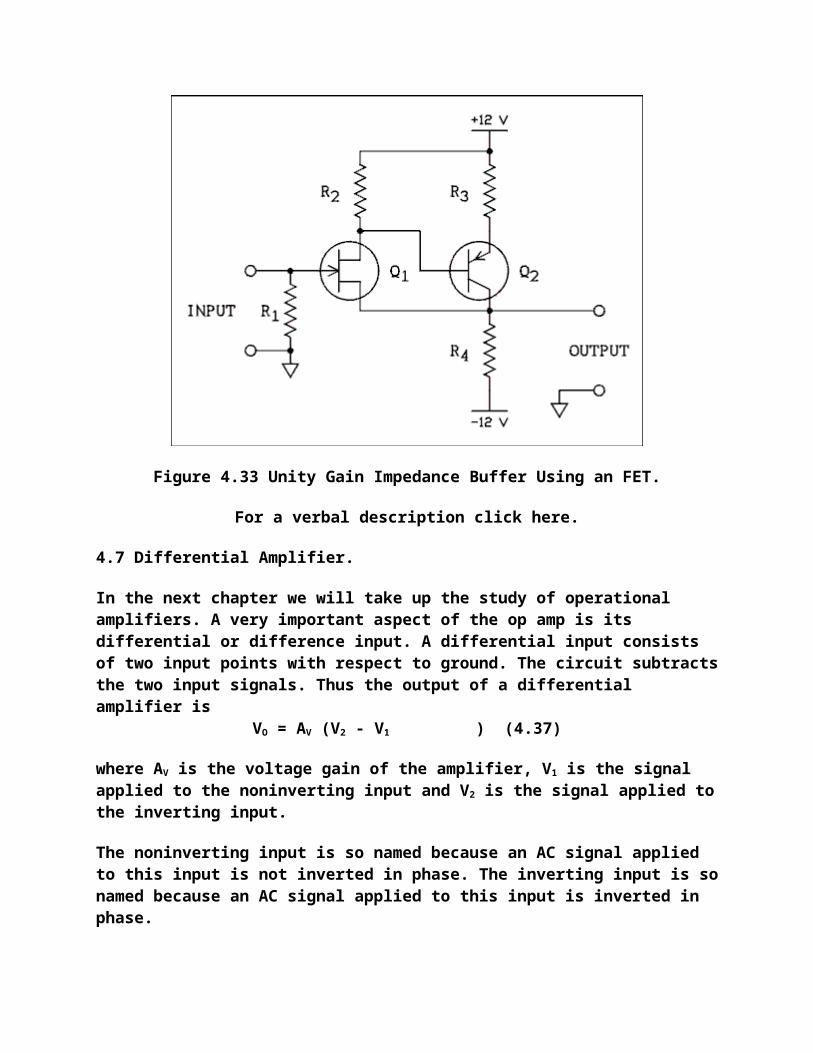
Figure 4B.7 Typical Converter From an AM Radio.
For a verbal description click here.
How the Converter Works.
The 6BE6/6SA7 converter has 5 grids making it a heptode or 7 element tube. Grids 2 and 4 are tied together inside the tube and grid 5 is tied to the cathode. That's how they can make
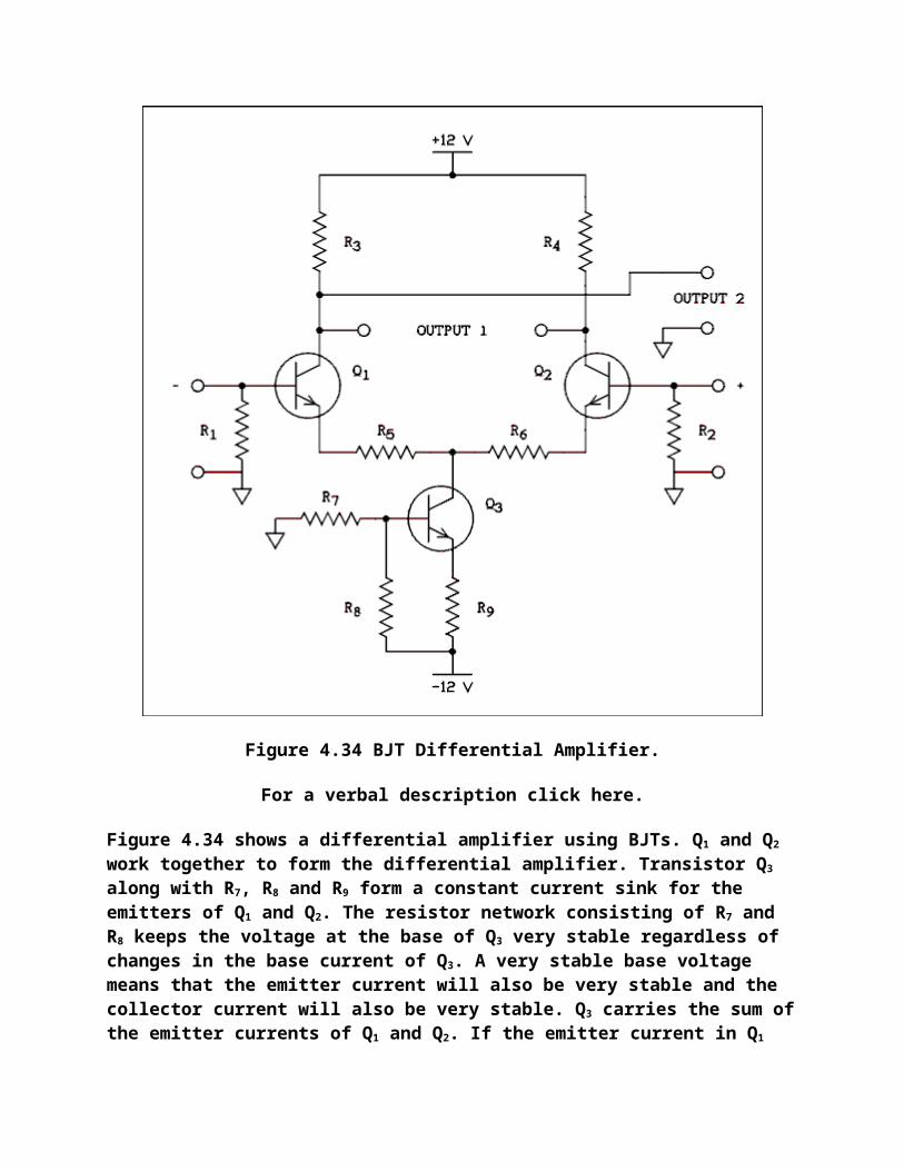
it work in a 7 pin tube. They need 2 pins for the heater leaving only 5 for the other elements of the tube. In the 6SA7 which has 8 pins, grid 5 is brought out to its own pin.
The cathode and the first two grids work like a triode tube and are the local oscillator. The circuit is called a Hartley oscillator because it uses a tapped inductor. (See section 4B.5). The cathode goes to the tap and the first grid, called the oscillator grid, receives signal which is coupled from the top of the oscillator coil. The cathode current flows through a few turns at the ground, or low, end of the coil. The magnetic field induces voltage in the rest of the coil. The coil is tuned by one section of the variable capacitor and the alternating voltage which appears across the coil has the frequency to which the coil is tuned. The voltage which is applied to the grid is enough to drive the cathode current of the tube from saturation to cutoff. The pulses of cathode current flow through the lower turns of the coil and maintain the oscillation. When the alternating voltage at the top end of the coil swings positive the grid is driven slightly positive and begins to conduct current like a diode. (The grid is attracting electrons to its self and therefore acts like the plate of a diode.) The 220 pf capacitor charges up so the most positive voltage at the grid is just barely positive and most of the time the grid voltage is negative. A DC meter connected to the grid with proper isolation so it won't short out the AC, will indicate the average voltage which may be anywhere from -5 to -40 volts. So the cathode current is flowing in short pulses at the oscillator frequency. Since the cathode is the only source of electrons in the tube the plate current is also flowing in short pulses with little or no current in-between pulses.
Grid 2 is connected to B+ and acts like a plate but it is a leaky plate. Electrons pass on through it to go on and be effected by the remaining 3 grids. Grid 3 is called the mixer grid and is where the station's signal comes in from the antenna. Because the oscillator signal is over driving the tube it is a nonlinear device and the sum and difference frequencies appear. Grid 4 is connected to B+ and so accelerates the electrons on there way to the plate.
Sometimes the impact of electrons on the plate causes electrons already there to be knocked loose. This is called secondary emission. If grid 5, called the suppressor grid, were not present these secondary electrons would go to the screen grid, grid 4, and take away from the plate current as described above. There are times in the AC cycle when the plate voltage is actually less than the screen voltage. The suppressor grid, which may be grounded or tied to the cathode, is negative enough to cause the secondary electrons to go back to the plate because they have no where else to go. The wires of grid 5 are widely spaced so it has little effect on the high velocity electrons on their way to the plate.
The tuned circuit in the plate of the converter tube is tuned to 455 kHz and is the primary of the first IF transformer. Short wave receivers are likely to have a higher intermediate frequency.
4B.3 The Beam Deflection Tube.
Like the Heptode, the Beam Deflection Tube was designed to perform a specific purpose. That is a balanced mixer, often called a balanced modulator. There are two types of balanced mixers, singly and doubly balanced.
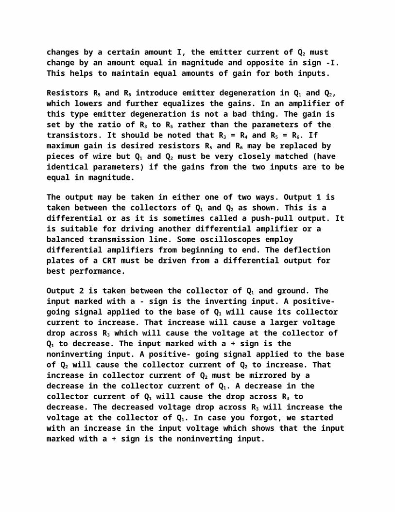
Doubly Balanced Mixers.
A doubly balanced mixer causes both input signals to be cancelled in the output. Going back to the original example if you supply signals of 5 and 6 MHz to a doubly balanced mixer the output will consist of the sum frequency of 11 MHz and the difference frequency of 1 MHz but the original frequencies of 5 and 6 MHz will be greatly attenuated.
Figure 4B.8 Doubly Balanced Mixer Implemented with Triodes.
For a verbal description click here.
An arrangement of 6 triodes, Figure 4B.8, will perform this function but tube drift makes it difficult to keep in balance and the attenuation of the original input signals may not be very high after a few weeks of operation. Automatic balancing circuits could theoretically be
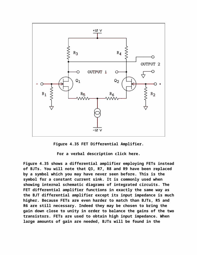
added but the already complex circuit would become so complex as to not be worth the trouble.
Figure 4B.9 DBM Integrated Circuit with External Circuitry.
For a verbal description click here.
An integrated circuit consisting of 9 transistors, Figure 4B.9, one used as a diode, carries the numbers MC1496, LM596, or NE5596, and is a very good DBM (Doubly Balanced Mixer). In an IC all transistors were manufactured at the same time and they are all at the same temperature in operation. Even the very slight amount of aging that occurs in transistors proceeds at the same rate for all of them. The writer has never tried to push its upper frequency limit but it will work up to 4 MHz. The circuit elements in red are external to the IC.
Figure 4B.10 DBM Implemented with Diodes.
For a verbal description click here.
An arrangement of 4 diodes and two transformers, Figure 4B.10, also makes a very good DBM. Its balanced depends on the exact matching of the diodes. Diodes are made in batches and all four must come from the same batch. Attempting to match diodes out of a large number of them will only result in matching at the test point and they will not give very good balance in a DBM. The characteristic curve of each diode must match over the entire current range from a few hundredths of a microamp to a milliamp or more. The only feasible solution is to purchase DBMs already put together and encapsulated with transformers and all.
Singly Balanced Mixer.
A singly balanced mixer will only cancel one of the two inputs. Diode versions can be constructed and because it only uses 2 diodes external DC biasing can be used to achieve balance. I don't think anyone has bothered to make prepackaged diode or IC versions.
In the late 50s there were two tube types made that would function as a singly balanced mixer. One, the 7360, was made for the specific purpose of generating single sideband suppressed carrier signals in communications equipment. The other, the 6AR8, was made to demodulate the chroma signal in color TV receivers. Both are shown schematically in Figure 4B.11.
Neither type is being manufactured today but because of supply and demand the 7360 is selling for about 10 times the price of the 6AR8.
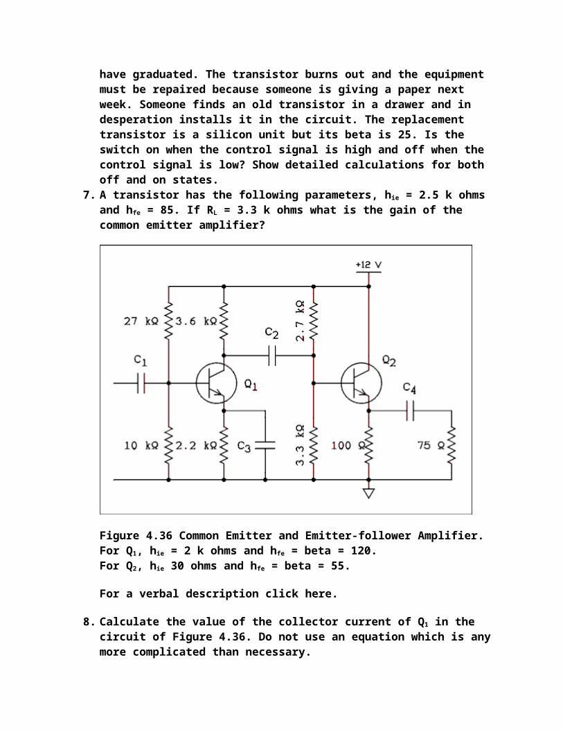
Figure 4B.11 Two Beam Deflection Tubes.
For a verbal description click here.
Other than which element goes to which pin the tubes are quite similar. The 6AR8 has a peculiarity in that one of the grids is tied to one side of the heater. The data on this tube states that pin 5 must be grounded. This grid is not even called a grid but an internal shield. Other than that the tube is perfectly normal.
In operation the electrons come out in a beam and if there is no potential difference between the two deflectors, the beam will strike both plates equally. An AC voltage applied to the control grid will cause an AC voltage to appear at the plates which is out of phase with the grid voltage but the voltage at the two plates will be in phase with each other.
For ease of understanding we will assume that both deflectors are driven with opposite phase voltages. This causes the electron beam to swing back and forth between the two plates. When the electron beam is on one plate that plate current will be high and the current on the other plate will be low. As the electron beam swings back the other way the current on the high current plate decreases and that on the low current plate increases. Thus the signals on the two plates are 180 degrees out of phase with each other.
To review then, the control grid causes in-phase voltages at the two plates, and the deflectors cause out of phase voltages at the two plates.
If there are two signals of different frequency applied to the control grid and deflectors the sum and difference frequencies will appear as for each plate the two signals are multiplied.
If the two plates were connected in parallel, the deflector voltage would be canceled while the control grid voltage would not. I have never seen a circuit like this. I suspect it produces quite a bit of distortion in this mode of operation.
Circuits I have seen connect the plates to the ends of a center-tapped transformer with B plus going to the center-tap. If you apply in-phase signals to the ends of a center-tapped
transformer, there is no net magnetic field and no, or very little, voltage is induced in the secondary. This means that the voltage applied to the control grid will be canceled in the output. This is a singly balanced mixer.
If you apply a radio frequency of say 455 kHz to the control grid and audio to one of the deflectors, as shown in Figure 4B.12, the RF signal will be canceled in the transformer. The audio will not be canceled but the output transformer is a tuned circuit at 455 kHz and the audio signal won't come through. Because this device is a mixer the sum and difference frequencies will be created. These are the sidebands of an AM signal but the carrier is suppressed. We are generating a double-sideband suppressed-carrier signal on 455 kHz. It could be heterodyned to any desired frequency.
Figure 4B.12 455 kHz Double-Sideband Suppressed-Carrier Generator.
For a verbal description click here.
The tube could also be used as a mixer in a receiver or transceiver in which canceling one of the input frequencies could reduce spurious signals. However, when this is a problem a doubly balanced mixer is usually preferred.
4B.4 Magic Eye and Cathode Ray Tubes.
Cathode ray tubes are familiar to most everyone. Only at this writing, 2007, are they disappearing from TV sets. Technically inclined people are also familiar with their use in oscilloscopes. They are also in the process of disappearing from that application.
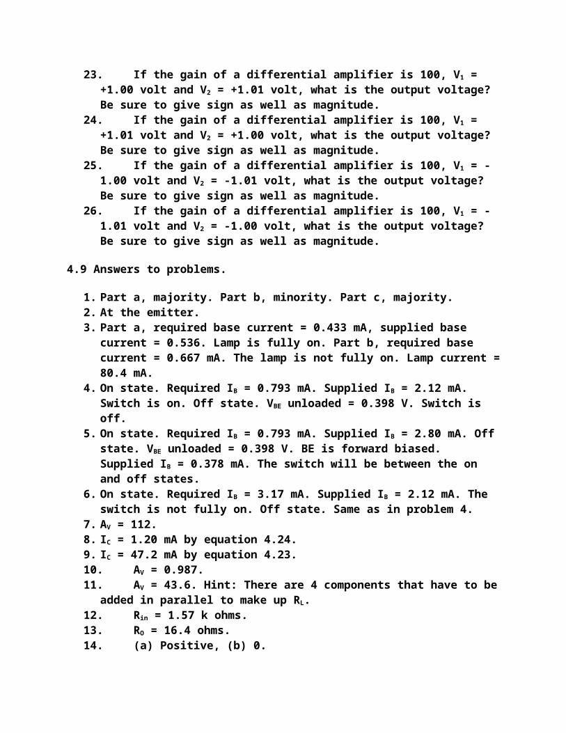
The Magic Eye Tube.
A magic eye tube is much less familiar although many readers may have seen one without realizing what they were looking at. Figure 4B.13 shows a magic eye tube. In A there is no power applied to the tube, in B it is fully open, and in C it is nearly closed. It can assume any state between open and closed depending on the applied voltage.
Figure 4B.13 The Magic Eye Tube in a Heathkit Capacitor Tester.
For a verbal description click here.
Here is the schematic diagram of a magic eye tube.
Figure 4B.14 Schematic of Magic Eye Tube Circuit.
For a verbal description click here.
The input goes to the grid of a triode amplifier which has a gain somewhere between 15 and 20 depending on tube type. When the voltage on the grid, pin 3, is zero the eye is fully open as shown in the left hand photograph above. Under these conditions the plate of the triode, pin 2 will be at about 25 or 30 volts.
As the grid voltage is made negative, the plate voltage increases and the eye moves toward being closed as shown on the right above. The plate of the right hand triode is called the target and is the anode which is coated with the phosphor material as seen in the top picture above. The phosphor glows green when bombarded by electrons.
The grid of the right hand triode is called the "Shadow Control Grid" in Figure 4B.15 below. It is connected internally to the amplifier plate. The voltage on the "Shadow Grid" varies from a low of 25 volts to approximately 60 % of B+.
Figure 4B.15 Construction of Magic Eye Tube.Not Exactly to Scale.
For a verbal description click here.
The target is not flat as it may appear in the drawing. It is shaped like a cup with a hole in the bottom. The angle of the sides coated with the phosphor is about 45 degrees. The "Shadow Rod" does exactly what its name implies, casts an electron shadow on the target. The "Shadow Rod" is connected to the cathode. When the "Shadow Control Grid" becomes more positive the "Shadow Rod" has less and less effect on the faster moving electrons and the shadow grows more narrow. The shadow rod and shadow control grid can be seen if you hold the tube at just the correct angle.
These tubes were used frequently as tuning indicators in deluxe radios from about 1935 into the 1950s. Most people could tune a radio by ear so their functionality was questionable.
The writer has heard a story, maybe true, maybe not, that some unscrupulous salesmen were telling people that if you looked into the eye and tuned in the station absolutely perfectly you could see what was going on in the radio studio. Nobody could ever achieve the level of perfection necessary to see Jack Benny, Bob Hope, et al.
Fraudulent claims not withstanding, the magic eye was used as a record level indicator on real to real tape recorders, (there weren't any other kind back then). It also turned up on a 2 meter transceiver as a modulation and power output indicator, as well as on an SSB exciter. Magic eye tubes have been used by radio hams and audio hobbyist in many applications for years.
The cathode ray tube.
The cathode ray tube is the familiar, although now disappearing, picture tube in TV sets and computer monitors. It has also enjoyed wide application in radar, and even as the numeric readout in an early electronic calculator. But perhaps the place where the CRT has found its best usage is in the oscilloscope.
If you told a service technician or maintenance engineer that he had to travel a great distance and work on an unknown piece of equipment, and he could only take one item of test gear, 999 out of 1,000 would take an oscilloscope. That 1,000th one would find himself up the proverbial creek without a paddle. An oscilloscope as it stands can measure voltage, time interval, and frequency. By the clever use of some resistors it can be used to measure current, resistance, capacitance and even transistor beta. Although there are digital multimeters that will measure all of these things the scope can still do something that no other test instrument can. That is show the shape of the wave. There are times when nothing will substitute for this.
The reader is referred to section 2.12 of this book for a detailed discussion of the cathode ray oscilloscope and its tube. There does not seem to be any point in repeating the information here.
4B.5 Oscillators.
The very first vacuum tube oscillator was probably built by accident when someone was trying to get just a little more gain out of a radio frequency amplifier. If the plate circuit of a triode amplifier is tuned slightly higher than the grid circuit oscillation will most likely result. A parallel tuned circuit appears inductive when tuned high and one that is tuned low appears capacitive. The oscillation will take place between the resonant frequencies of the grid and plate circuits. The phase shifts that result will cause the feedback through the plate to grid capacitance to have a phase close enough to correct to sustain oscillation.
TGTP (tuned plate tuned grid) oscillators are never used because changing the frequency requires turning the variable capacitors in two tuned circuits. If you want to play with one it usually helps to supplement the plate to grid capacitance with an external capacitor of 10 pf or so. If you use a pentode, the external capacitor is an absolute must.
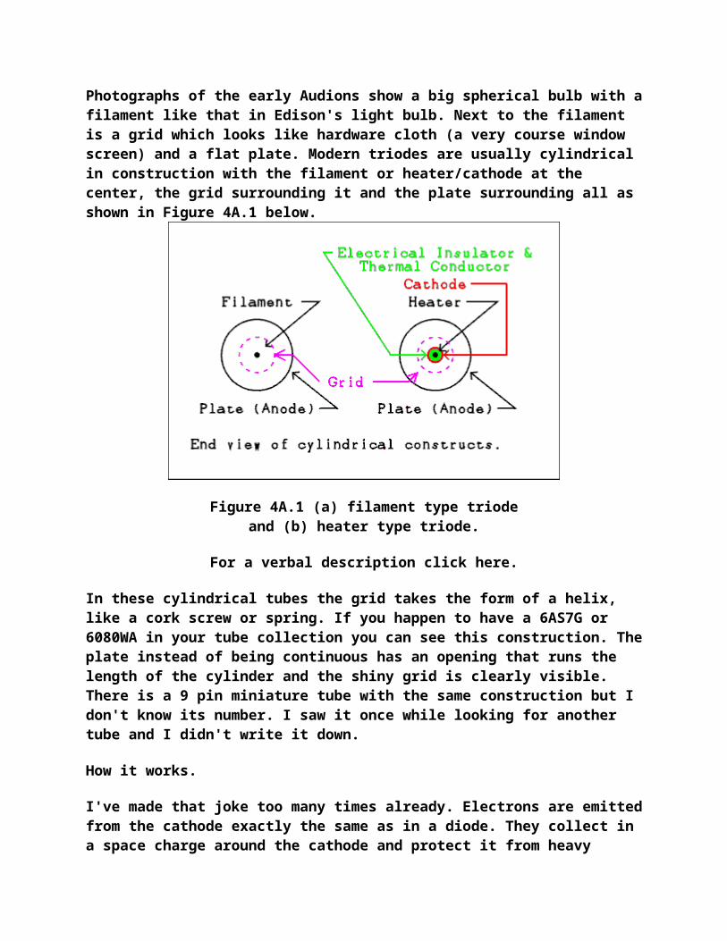
Colpits and Hartley Oscillators.
The Colpits oscillator is distinguished by the fact that the capacitor is split in half and the junction of the two halves is often, although not always, connected to ground.
In the Hartley oscillator the inductor is tapped and the tap may or may not be connected to AC ground. It also may or may not be connected to DC ground.
Figure 4B.16a shows a parallel fed Colpits oscillator. It is parallel fed because the DC plate current does not flow through the inductor. R3 may be replaced by an RF choke if desired. C3 keeps B+ from appearing across the variable capacitor which is generally a no no. If R1 were not present, C3 might not charge up and there would be B+ on the variable capacitor anyway. R1 makes sure that the inductor and the outer plates of the variable capacitor are held at DC ground potential. The tuning capacitor is sometimes known as a split stator but is actually the familiar dual ganged capacitor. The rotor and drive shaft are at both AC and DC ground potential.
The capacitor is, in effect, center tapped. This will place the center of the coil at AC ground potential. The effect of this is to cause the AC voltage at one end of the tuned circuit to be 180 degrees out of phase with the AC voltage at the other end. Since the plate voltage is 180 degrees out of phase with the grid voltage, the voltage fed back to the grid has the proper phase to reinforce and sustain oscillation.
The two halves of the variable capacitor need to be the same size or in a constant ratio to one another. If the oscillator is to be tuned over a narrow range, the capacitor on the plate side may be fixed and the variable capacitor on the grid side would have a fixed capacitor in parallel with it to limit its tuning range.
The AC voltage supplied to the grid is considerable. On the positive peak it drives the grid positive and C2 will be charged. When the grid is forced positive it begins to attract electrons to itself and current will flow. The grid acts like the anode of a diode. This current causes the capacitor to charge with the end of the capacitor which is toward the grid being negative. The grid never goes very far positive because the capacitor charges up and holds the charge. A small amount of charge leaks off through R2 but gets replenished on the next positive half cycle. A substantial average DC voltage, as much as -50 volts, is developed at the grid and this voltage makes the oscillator self adjusting. The negative bias lowers the gain of the tube and it will set itself to exactly what is needed to sustain oscillation. When the grid voltage goes negative, in most oscillators this will drive the tube into cutoff. This will cause the plate current to flow in short pulses but the tuned circuit rings like a bell and the waveform at the grid is a very good sine wave. The wave at the plate may not be as good.
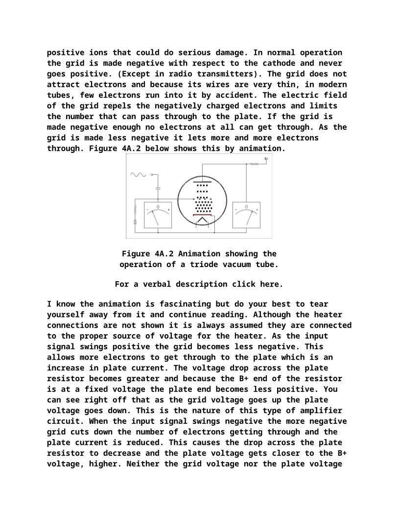
Figure 4B.16 Parallel fed Colpits (a) and Hartley (b) oscillators.
For a verbal description click here.
Figure 4B.16b shows a series fed Hartley oscillator. Once again an RF choke could be used to replace R2. Capacitor C3 blocks the B+ voltage from the tuned circuit. Because the center tap of the coil is grounded there is no need for a resistor to ground. Neither side of the variable capacitor is at AC ground potential. An insulated coupling must be used between the capacitor shaft and tuning knob shaft to avoid the effect of hand capacitance. Hand capacitance would cause the frequency of the oscillator to shift when a person's hand came near the tuning knob.
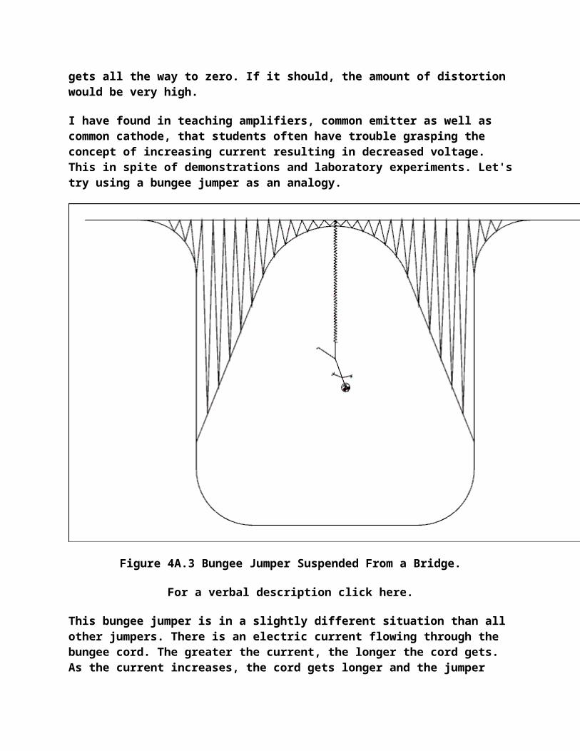
Figure 4B.17 Two Series Fed Hartley Oscillators.
For a verbal description click here.
Series fed oscillators are more efficient and stable because there is no resistor in parallel with the tuned circuit to lower the Q. In figure A the B+ is tied to the center tap of the coil. This has the effect of placing both sides of the tuning capacitor at B+ potential. Even with insulated couplers from the capacitor shaft to the tuning shaft the "hot" capacitor is a hazard to someone servicing the equipment. That is why the tuned circuit has been moved to the cathode side of the tube as shown in B.
This is still a series fed circuit because the cathode current flows through the coil. You will note that the tap has been moved from the center to near one end and that end of the coil has been grounded. This removes B+ from the capacitor and permits the drive shaft to be at ground potential.
The reason for moving the tap has to do with gain around the loop. A center tapped inductor gives phase inversion and unity gain. With the tuned circuit connected from plate to grid the tube provides gain enough to ensure the oscillator will start and keep going. In figure 4B.17b the tube is now a cathode follower which has a little less than unity gain. The coil acts as an auto transformer and steps up the voltage applied to the tap. The top to tap ratio is typically 10 to 1. The cathode follower does not invert the phase and neither does the coil since both connections are on the same side of the ground point.
The cathode coupled series fed Hartley oscillator has become the most popular oscillator circuit among receiver design engineers. In addition to the ubiquitous All American 5 it is found in short wave, and ham receivers from about 1940 on.
Figure 4B.18a shows a parallel tuned Colpits Oscillator. The inductor labeled RFC is an RF choke. It is used in place of a resistor to provide a high impedance to the oscillator and at the same time a low DC resistance. The tuned circuit requires a high parallel impedance. If a resistor were used it would have to be of such a high value as to reduce the plate current of the tube to a very low value. If it were lowered to get the plate current up it would adversely effect the Q of the tuned circuit.
Figure 4B.18 Two Colpits Oscillators.
For a verbal description click here.
Figure 4B.18b shows a series tuned Colpits circuit which is often referred to as a Clap oscillator. Wipe off that silly grin. Like the Hartley and Colpits circuits, the Clap circuit was named after the man who invented it. Capacitors C3 and C4 are comparatively quite large. I have seen circuits in which they were 0.005 microfarads. To resonate with these capacitors at 4 MHz the inductor would have to be quite small, 0.633 microhenrys to be exact. Such a small inductor would be about one turn and would have a low Q at 4 MHz. In actuality the series tuned circuit has a normal inductor of many turns and a capacitor of 100 or 200 pf.
Remember that a series tuned circuit has minimum impedance at resonance. Just a little off resonance, on the high side, it is still a low impedance but appears inductive. A low inductive reactance means a small apparent inductance. It may seem as if the Q is low but the basic LC circuit has a high Q which will make the oscillator very stable.
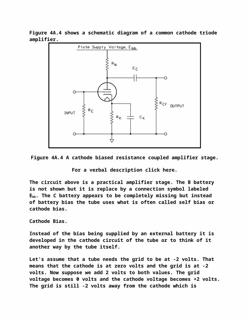
Oscillator Stability.
There is nothing in the diagram of an oscillator that would indicate it would be anything but perfectly stable. That is, you could set it to a given frequency and it would stay there forever. The reality of oscillators is not even close to that. An LC oscillator will drift in frequency and unless steps are taken to minimize the drift it may be unusable for the desired function.
As the last sentence of the previous paragraph indicates, the drift of an oscillator can't be eliminated, just minimized. Let's first examine the causes of drift and then see how they can be minimized.
The main cause of frequency drift is a change in temperature. In vacuum tube equipment the heat generated by the tubes is unavoidably transferred to the elements of the tuned circuit.
As the inductor warms up the wire making up the coil gets longer. The form on which the coil is wound gets larger in diameter, and all that translates into a larger inductance.
In an air capacitor such as a variable, The plates get bigger and farther apart. Those two effects may seem to cancel each other and they do to some extent. In ceramic and mica capacitors the dielectric, (insulator), usually has a temperature coefficient all its own. This can be adjusted by the manufacturer to give a capacitor a positive, zero, or negative temperature coefficient.
The coil is sitting there with its big positive temperature coefficient so if we can incorporate a negative coefficient into the resonating capacitor this will go a long way toward making the oscillator stable.
Another source of instability is the change in tube capacitance. This change occurs much faster than those caused by warming up of the coil and capacitor. An attempt to compensate for changes in tube capacitance could result in an oscillator that would drift down in frequency until the tube reaches its operating temperature and then up as the coil and capacitor start to feel the heat from the tubes.
The trick here is to make the fixed capacitors in the circuit so large that the tube capacitances will be a small part of the total. In any of the circuits the capacitor can be made larger and the inductor smaller. This can only be carried so far. This will result in a lower Q because a coil which is too small for the frequency will have more resistance in relation to its inductance.
The parallel tuned Colpits goes somewhat in this direction. The ARRL Radio Amateurs Handbook recommends for an oscillator to tune from 3.5 to 4 MHz, that C3 be 680 pf and C4 be 0.0022 uf. For the Clap oscillator they recommend that C3 and C4 both be 0.001 uf. Although the writer once owned a VFO, (Variable Frequency Oscillator), made by E. F. Johnson that used 0.005 uf capacitors for C3 and C4.
Electron Coupled Oscillator, (ECO).
You may be wondering how to get the signal out of these oscillators. In all cases the best waveform is found at the grid although this is a very high impedance point and a lot of isolation would have to be included to keep changes in load from effecting the frequency. For the cathode coupled circuits the output signal could be taken from the cathode which is a low impedance point. Even so changes in load can cause the frequency to change quite a lot. The solution is to use a pentode and take the signal off the plate, as shown in Figure 4B.19.
Figure 4B.19 Electron Coupled Clap Oscillator.
For a verbal description click here.
This is called an Electron Coupled Oscillator because the screen grid takes the place of the plate in the triode circuit and the signal is coupled to the plate by the electrons that pass through the screen.
Notice that the screen voltage needs to be regulated and it doesn't hurt to regulate the plate voltage as well. The tuned circuit in the plate serves to clean up the waveform which is not a good sine wave if a resistor is used. R2 lowers the Q of L2 and C6 so it does not have to be tuned along with C1 and L1.
This oscillator can be plugged into the crystal socket on a 50 or 75 watt transmitter. If used as part of a transmitter it should be followed by a class A pentode stage before going into
the class C stages. If used in a receiver or transceiver the output could probably be fed straight to the mixer.
Crystal Oscillators.
One solution to oscillator drift is to use a quarts crystal. If quarts crystals are cut in a certain way they are piezoelectric. Which means that if an electric field is placed across them, one or more of its mechanical dimensions will be altered. Conversely, if mechanical force is applied an electric potential will be developed. The process is known as bilateral which means it works both ways.
The crystal is cut into thin rectangular plates along a particular axis of the crystal. The subject of quarts crystals can fill a book all its own. No attempt will be made here to delve into the various orientations in which a crystal can be cut.
Every physical object has a mechanical resonant frequency. Some are low enough to hear such as a common drinking glass filled, or partly filled, with water. Early TV remote controls used aluminum rods about 3/8 inch in diameter and about 2 inches long. When one of these rods was struck on the end it would ring at a frequency above the range of human hearing. A specially designed microphone in the TV set would pick up the ultrasonic frequencies and after amplification a set of tuned circuits allowed the particular rod being struck to initiate the corresponding function. The tiny plates of quarts have mechanical resonant frequencies that are in the radio frequency range. When this mechanical resonance is translated into electrical resonance by the piezoelectric effect, the crystal exhibits the resonance of the circuit of Figure 4B.20a.
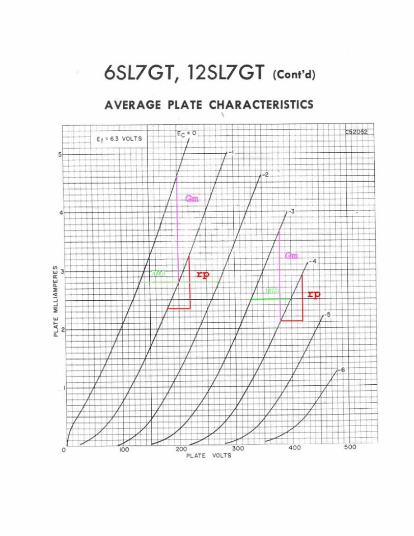
Figure 4B.20 (a) Equivalent Circuit of a Quartz Crystal,and (b) Colpits Crystal Oscillator.
For a verbal description click here.
Because the series resonant circuit has a capacitor in parallel with it the overall effect is for the crystal to have a very low impedance at its series resonant frequency, and just a few hertz higher, a high impedance at its parallel resonant frequency. When ordering crystals you must specify which of the resonant modes you plan to use and if parallel, how much capacitance will be across the crystal.
Figure 4B.20b is the circuit of a Colpits oscillator. It operates the crystal in its parallel resonant mode. There are many crystal oscillator circuits but this is by far the best one for almost all crystals. Typical values for the capacitors are 33 pf for grid to cathode and 100 to 220 pf for cathode to ground.
The output may be taken off the cathode or if a cleaner waveform is desired a pentode may be used with a tuned circuit in its plate circuit as shown in figure 4B.19 above.
There is only one way to change the frequency of a crystal oscillator. Order a new crystal and when it comes in the mail, plug it into the socket. That's the price to be paid for a high degree of stability. In Chapter 9 of this book we will study the frequency synthesizer which gives both the agility of a tunable oscillator and the stability of a crystal oscillator. It would not be practical to construct one of these devices with vacuum tubes.
4B.6 Problems.
1. The plate resistance of the pentode section of a 6U8 is 0.4 Meg ohms. The RC amplifier data for it is as follows.
Ebb = 250 volts.Rb = 270 k ohms.Rcf = 1.0 Meg ohms.Rc2 = 820 k ohms.Rk = 1200 ohms.Vin = 0.1 v.Vout = 22.0 v.Gain = 220.% Dist = 0.82 %.
Calculate (a) the transconductance of the pentode under the above conditions, and (b) the gain of the amplifier if the cathode bypass capacitor is removed and the screen is bypassed to the cathode.
2. A ham band receiver has a first IF of 2250 kHz, and the local oscillator operates above the incoming frequency. If the receiver is tuning the 3.5 to 4.0 MHz band what is the frequency range of the image?
3. A doubly balanced mixer has the following input frequencies, 3.5 MHz, and 60 kHz. What frequencies will be present in its output?
4. A singly balanced mixer has the following input frequencies, 1.5 MHz to the balanced input, and 2.5 MHz to the unbalanced input. What frequencies will be present in its output?
5. The AGC voltage of a radio receiver is about -1 volt between stations and changes to -10 volts when a particular station is tuned in. A tuning eye (magic eye tube) in this radio will be,
(a) closed when between stations and open when a station is tuned in.
(b) open when between stations and closed when a station is tuned in.
6. A wave on an oscilloscope is 3.4 cm from the lowest to the highest point and 2 complete cycles cover 8.7 cm. The controls on the scope are set as follows. Vertical to 50 milli volts/cm and time-base to 20 nsec/cm. A times 10 probe is in use. What is the RMS voltage of this wave?
7. A wave on an oscilloscope is 3.4 cm from the lowest to the highest point and 2 complete cycles cover 8.7 cm. The controls on the scope are set as follows. Vertical to 50 milli volts/cm and time-base to 20 nsec/cm. A times 10 probe is in use. What is the frequency of this wave?
8. An oscillator with a tapped coil is a;
(a) Hartley.
(b) Colpits.
(c)Clap.
9. An oscillator with the inductor and variable capacitor in series is a;
(a) Hartley.
(b) Colpits.
(c)Clap.
10. In an oscillator employing a tapped coil, When the coil is connected to the plate and grid the tap is;
(a) at the center of the coil.
(b) near one end.
11. In an oscillator employing a tapped coil, When the coil is connected to the cathode and grid the tap is;
(a) at the center of the coil.
(b) near one end.
12. In any of the oscillator circuits employing a triode tube the best waveform is found at;
(a) the cathode.
(b) the grid.
(c) the plate.
13. In an ECO the signal is coupled from the oscillator to the output by;
(a) capacitive coupling.
(b) magnetic inductive coupling.
(c) the electrons inside the tube.
4B.7 Answers to Problems.
1. (a) 1,585 micro mhos, (b) 98.0. 2. 8.0 MHz to 8.5 MHz. 3. 3440 kHz and 3560 kHz. 4. 1.0 MHz, 2.5 MHz, and 4.0 MHz. 5. (b) 6. 1.7 volts. 7. 11.5 MHz. 8. (a) 9. (c) 10. (a) 11. (b) 12. (b) 13. (c)
This page copyright © Max Robinson. All rights reserved.
Applying Feedback To Amplifier Circuits. Chapter 5
Some Preliminary 5.1 Information. The Negative 5.2 Feedback Equation. The Special 5.3 Case of the Inverting Amplifier. 5.4 Frequency Response and Stability. Gain Accuracy and Precision. 5.5 Other Benefits of Negative 5.6 Feedback. Some Practical 5.7 Circuits. Positive Feedback, 5.8 Oscillators. Problems. 5.95.10 Answers to Problems.
Chapter 5.Applying Feedback To Amplifier Circuits.
If you have ever operated your school's sound system or have participated in a rock or country music band, you probably know the word "feedback". Feedback occurs when a fraction of the output signal is introduced into the input of an amplifier. The kind of feedback that sound system operators are familiar with is the squeal of positive feedback. This kind of feedback is undesirable but there are kinds of feedback which cause good things to happen. In this chapter we will study the desirable kinds of feedback.
5.1 Some Preliminary Information.
When feedback is introduced electronically its phase can be controlled. The signal which is fed back may reinforce or partially cancel the input signal. Feedback which reinforces the input signal is called positive feedback. Feedback which partially cancels the input signal is called negative feedback. We will begin our study of feedback with negative feedback.
A major confusion factor has developed in teaching negative feedback because of a split among electrical engineers. One group, the audio engineers, sets out to derive the feedback equation by assuming a generalized amplifier. The equation they derive has a minus sign in the denominator. The other group, control systems engineers, assumes a net 180 degree phase shift in the feedback loop. In other words they assume that the feedback is always negative. The equation they derive has a plus sign in the denominator.
That would be bad enough by itself but the operational amplifiers (op amps) which are so useful have grown out of the control systems branch of electrical engineering. What this means to a teacher teaching a survey course in electronics is that when teaching feedback applied to audio amplifiers the equation with the minus sign must be used and when
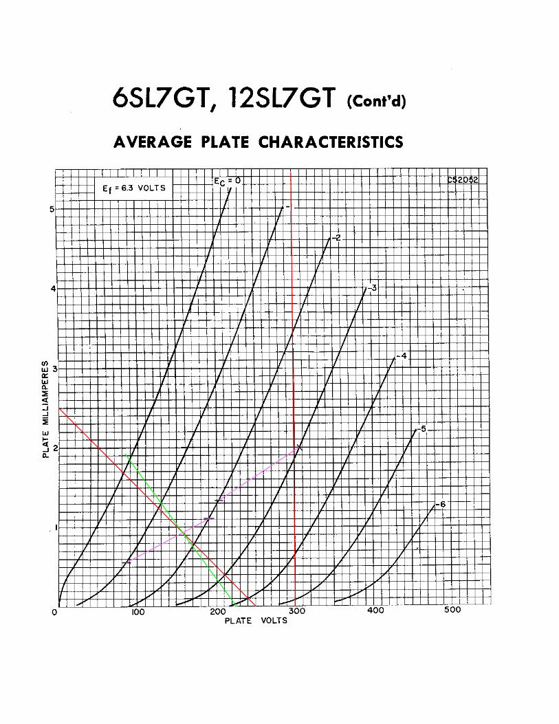
teaching op amps the equation with the plus sign must be used. That has proven to be so confusing to students that there is doubt as to whether they ever learned anything about feedback. In this book we will define away the problem by adopting one convention and sticking to it. If you look up the subject of feedback in another textbook you may find more confusion than help.
5.2 The Negative Feedback Equation.
Figure 5.1 Noninverting Amplifier with Negative Feedback.
For a verbal description click here.
Figure 5.1 shows an amplifier with negative feedback applied. The amplifier is a differential amplifier which was discussed in the closing section of chapter 4. The signal generator is applied to the noninverting input of the amplifier. A fraction, beta, of the output signal is fed back to the inverting input. The difference between the two signals is amplified by the factor A and appears at the output.
The output of a differential amplifier is given by equation 4.27 which is repeated here.
VO = A (V1 - V2 (5.1) ) As shown in Figure 5.1 V1 is the input signal and V2 is the fraction of the output signal beta VO. If we make these substitutions into equation 5.1 we have
VO = A (VIN - beta VO (5.2) ). Solving this equation for VO / VIN we have the feedback equation.
VO / Vin (5.3) = A / (1 + A beta) The term VO / VIN is called the closed loop gain and is given the symbol A', thus,
(5.4) A' = A / (1 + A beta) where A' is the closed-loop gain, A is the open-loop gain and beta is the fraction of the output which is fed back to the input. This equation is to amplifiers as Ohm's law is to electric circuits. Memorize it.
For the noninverting amplifier beta is given by
beta = R1 / (R1 + R2 (5.5) ) This beta is not to be confused with the BJT beta. They are not the same thing nor are they related in any way.
Let us be sure we understand all of the terms associated with feedback. The open-loop gain (A) is the gain of the amplifier without any feedback circuits connected. The closed-loop gain (A') is the gain of the amplifier after the feedback has been connected. Beta, (it has no other name,) is that fraction of the output which is fed back to the input.
Example 5.1.
An amplifier has an open-loop gain of 250 and a beta of 0.02. What is its closed-loop gain?
Solution:
The closed-loop gain is given by
A' = A / (1 + A beta) = 250 / (1 + 250 x 0.02) = 41.67.
Note that we indicate this gain as a positive number. The circuit of Figure 5.1 is a noninverting amplifier which has no phase inversion. Such an amplifier has the signal applied to the noninverting input.
5.3 The Special Case of the Inverting Amplifier.
When the signal is applied to the inverting input, the circuit is called an inverting amplifier. An AC signal applied to the amplifier will be inverted by 180 degrees. When the value of the gain is stated it must be given as a negative quantity. The circuit of an inverting amplifier is shown in Figure 5.2. If you look in other texts similar to this one you are not likely to find the derivation of the gain of an inverting amplifier. The reason is that the equation which results from an exact derivation is slightly different from the one for a noninverting amplifier. Let us derive the equation and then we will discuss the difference.
Figure 5.2 Inverting Amplifier with Equation Loops Indicated.
For a verbal description click here.
In Figure 5.2 the loops and polarity of all voltage drops are clearly marked. Consider these markings as a "snapshot" taken at the peak of the sine wave. Current flows from left to right through R1 and R2 thus causing the voltage drops to be as indicated on R1 and R2. Because of the nature of the amplifier the output voltage (VO) must have the opposite polarity as the input voltage (Vsig).
If we write the loop equations around the loops labeled "equation 5.5" and "equation 5.6" we have
VIN = I R1 + Vsig (5.5) And
Vsig = I R2 - VO (5.6) . The current I is the same in both resistors. The input resistance of the amplifier is very high and in actual practice the magnitude of Vsig is very small; hence any current flowing into the inverting input is very, very small. Therefore the currents in R1 and R2 are equal. Solving equations 5.5 and 5.6 for I and setting them equal gives
(VIN - Vsig) / R1 = (VO + Vsig) / R2 (5.7) The nature of the amplifier requires that VO = A Vsig; therefore, Vsig = VO / A. Making this substitution into equation 5.7 gives.
(VIN - VO / A ) / R1 = (VO + VO / A) / R2 (5.8) If we multiply equation 5.8 through by A, R1 and R2 we get
R2 VIN A - R2 VO = R1 VO A + R1 VO (5.9) . After collecting VO terms, factoring out VO and performing some additional algebraic calisthenics we get
VO / VIN = R2 A / (R2 + R1 A + R1 (5.10) ) Remembering that A' = VO / VIN and dividing numerator and denominator by R2 gives.
A' = A / (1 + R1 / R2 A + R1 / R2 (5.11) ) For the inverting amplifier we will now define beta as follows.
beta = R1 / R2 (5.12) If we substitute equation 5.12 into equation 5.11 and factor out beta we now have,
(5.13) A' = A / (1 + beta (A + 1)). Compare equation 5.13 with equation 5.4 which is the gain for a noninverting amplifier.
You are challenged to find equation 5.13 in any other text on this level. If all starting assumptions are correct and all of the algebra has been correctly done, the solution must be correct. Careful laboratory measurements using an amplifier with a low open-loop gain have shown that the equation does accurately predict the gain of an inverting amplifier. Equation 5.13 is the correct equation for the gain of an inverting amplifier.
A Difference Which Makes No Difference Is No Difference.
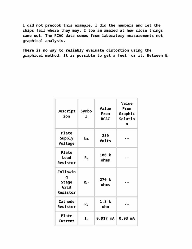
If the open-loop gain A is much greater than unity, equation 5.13 may be approximated by equation 5.4 with little detectable error. In actual practice open-loop gains are almost never less than 200 and may be as high as 107. Adding one to these large numbers will not make any practical difference. Unless the open-loop gain is less than 50, you need not bother with equation 5.13. Use equation 5.4.
Example 5.2.
An inverting amplifier has an open-loop gain of -10. The values of the feedback resistors are R1 = R2 = 10 k ohms. (a) What gain is predicted by equation 5.4? (b) What gain is predicted by equation 5.13? (c) What is the percent error of equation 5.4?
Solution:
For an inverting amplifier beta = R1 / R2 and if R1 = R2, beta = 1.00. (a) The gain predicted by equation 5.4 is.
A' = A / (1 + A beta) = 10 / (1 + 10 x 1) = -0.9091.
(b) The gain predicted by equation 5.13 is.
A' = A / (1 + beta ( A + 1)) = 10 / (1 + 1 x 11) = -0.8333.
(c) The result of equation 5.13 is the standard; therefore, the percent error is + 9.10%
Example 5.3.
An inverting amplifier has an open-loop gain of -500. R1 = 10 k ohms and R2 = 200 k ohms. What is the closed-loop gain of the amplifier?
Solution:<
The value of beta is beta = R1 / R2 = 10 k ohms / 200 k ohms = 0.0500. The open-loop gain is so much greater than unity that we can use equation 5.4.
A' = A / (1 + A beta) = 500 / (1 + 500 x 0.05) = -19.23.
Example 5.4.
A noninverting amplifier has the same values as in example 5.3, A = 500, R1 = 10 k ohms and R2 = 200 k ohms. What is the closed-loop gain?
Solution:
For a noninverting amplifier the value of beta is
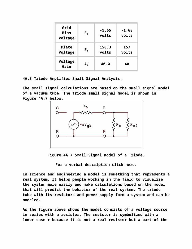
beta = R1 / (R1 + R2) = 10 k ohms / (10 k ohms + 200 k ohms) = 0.047619
The closed-loop gain is.
A' = A / (1 + A beta) = 500 / (1 + 500 x 0.047619) = +20.15.
5.4 Frequency Response and Stability.
Until now we have treated amplifiers as having a phase shift of 0 degrees (noninverting) or 180 degrees (inverting). As long as the frequency response is flat (gain does not change with frequency), these rules of phase shift apply. If the gain is rising or falling with frequency, there will be an extra phase shift which may cause trouble.
The gain of an amplifier will change with frequency if there are RC networks inside the amplifier. These circuits may have been introduced intentionally or they may just be there. An example of an intentionally introduced RC circuit is the coupling capacitor between the collector of one BJT and the base of the next BJT. The resistance in the circuit and the capacitor form a high-pass filter. A semiconductor amplifier may not have any, or maybe one, of these circuits but a vacuum tube amplifier may have several.
Something never shown in schematic diagrams but always present in real circuits is stray capacitance. Remember that a capacitor consists of two conductors separated by an insulator. Any time there are two wires close together there is capacitance between them. That means that there are invisible capacitors connected from the collector of each transistor to ground and from the base of every transistor to ground. These capacitors combine with the Thevenin's resistance of the circuits to form low-pass filters. Each tiny low-pass filter causes the frequency response of the amplifier to roll off (gain decreases as frequency increases). Moreover, each transistor (BJT or FET) has its own built-in low-pass filter. Each device has its own frequency limits which are imposed by such things as collector-to-base capacitance and charge mobility within the semiconductor material.
The equations for phase shift (chapter 2) tell us that at the cutoff frequency the phase shift is 45 degrees. As the frequency gets higher than the cutoff frequency of a low- pass filter (or lower than the cutoff frequency of a high- pass filter) the phase shift quickly approaches 90 degrees. At the same time the gain is falling at a rate of a factor of 10 for each factor of 10 change in frequency.
Because the individual RC filters are isolated from one another by transistor stages, each one contributes to the total without affecting each other. If there are two RC filters with similar cutoff frequencies, the gain beyond cutoff will change by a factor of 100 for every factor of 10 change in frequency. The phase shift will approach 180 degrees. If there are three RC filters, the gain will change by a factor of 1000 for every factor of 10 change in frequency and the phase shift will approach 270 degrees. Gain change and phase shift go together like many other pairs of things you may have heard of. "You can't have one without the other." Thus, it is possible to know what the phase shift is even if you have no way of measuring it directly.
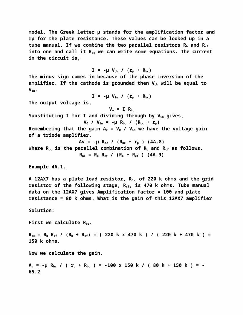
In the common operational amplifier, (op amp), the collector of the preceding transistor stage is directly coupled, not capacitively coupled, to the base of the next stage. This makes the frequency response go down to zero frequency which is DC. This is one of the few cases in electronics where it is possible to get something all the way to zero. Without any high pass filters in the amplifier the low pass filters that make the response roll off at the high frequencies are our only concern.
In some transistor amplifiers and all vacuum tube amplifiers there are high pass filters between each stage. These are capacitors in series with the signal path which are necessary to block the DC on the plate or collector of one stage from altering the bias on the grid or base of the following stage. The capacitors in conjunction with the resistors that connect to the control element of the amplifying device form high pass filters. These High-pass filters introduce phase shift and can cause low frequency oscillation if not designed properly.
The amount of phase shift depends upon the rate at which the gain is changing with frequency, which is determined by how many RC low-pass (or high-pass) circuits there are inside the amplifier. The rate of gain change is geometric. This means that a changing gain will be a straight line on a log- log graph. Figure 5.3 shows a log-log graph with various slopes (rates of change) plotted on it.
A rate of change of one decade decrease in gain for each decade increase in frequency is referred to as a slope of -1. If the gain decreases two decades for one decade increase in frequency, the slope is -2. If the gain should be increasing as frequency increases, the slope would be positive.
In the following discussion the phase shifts will be given with respect to the noninverting input. The phase shifts for the inverting input will be the algebraic sum of the stated phase shift and 180 degrees. If the slope of the frequency response is a negative 1, the phase shift will be -90 degrees. If the slope of the frequency response is -2, the phase shift will be -180 degrees. If the gain is falling with a slope of -2, the noninverting and the inverting inputs will be effectively interchanged. A connection which we thought would give negative feedback instead gives positive feedback. Positive feedback is the situation wherein the input signal is reinforced by the signal which is fed back instead of being partially canceled. When the input signal is reinforced, the output signal increases in amplitude. This causes the fed back signal to be increased which, in turn, causes the output signal to increase. This is a run- away condition and the input signal is no longer necessary; the amplifier is supplying its own input. An example is the earsplitting squeal of a sound system. This process is called oscillation and a device which oscillates is called an oscillator. When negative feedback becomes positive feedback we have an oscillator instead of an amplifier.
It would do no good to reverse the connections to the inverting and noninverting inputs. There would always be a part of the frequency spectrum where the gain is flat and there would be no extra phase shift. The circuit would oscillate because the feedback would be positive for those frequencies where the frequency response is flat.
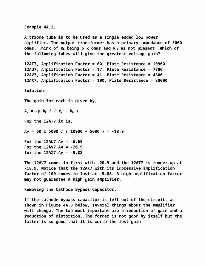
In order to support oscillation two conditions must be met: 1) the net phase shift around the feedback loop must be zero and 2) the gain must be greater than unity. In order to prevent a feedback amplifier from oscillating, we must see to it that both conditions are not met at the same frequency. If at any given frequency only one of the two conditions is met, oscillation will not occur. The act of making internal changes to the amplifier so that both conditions will not be met at the same frequency is called amplifier compensation.
An amplifier which has not been compensated may well have a frequency response like that of the black line in Figure 5.3. A properly compensated amplifier could have a frequency response like the green line in the figure.
Figure 5.3 Bode Diagram Showing Compensation of an Amplifier.
For a verbal description click here.
It should be pointed out that the slope of real frequency response curves does not break suddenly from one slope to another. The curves make gradual and smooth transitions from one slope to the other as we saw in chapter two. What has been drawn in Figure 5.3 are the tangents to the curves. The tangents from the flat portion and the -1 slope portion intersect directly over the -3 dB point. That is why the -3 dB frequency is sometimes called the corner frequency.
Examine the black curve in the above figure. It goes out flat to 100 kHz. Actually the frequency response is down 3 dB at 100 kHz but the Bode plot is drawn this way. At 100 kHz the plot breaks to a slope of -1. That means that one of the transistors started rolling off the frequency response. Another transistor in the amplifier begins to roll off at 1 MHz. This causes the Bode plot to break to a slope of -2. The plot falls by 40 dB, a factor of 100, between 1 and 10 MHz. At 10 MHz another transistor kicks in and the slope breaks to a slope of -3. After that the curve falls by 3 decades, 60 dB between 10 and 100 MHz.
What makes a feedback circuit oscillate is the loop gain not the gain of the amplifier. If this amplifier were to be used with a beta of 1/10000, it would not oscillate. 10000 is the value of gain where the slope breaks from -1 to -2. If a gain of 10000 is combined with a beta of 1/10000 the value of A beta is unity where the Bode plot breaks from -1 to -2 and the amplifier will be stable. Such a small value of beta would not be very useful but in audio amplifiers where the value of beta is fixed by the designer and does not change the Bode plot for A beta is used to compensate the amplifier instead of the plot of A alone.
On the other hand an op amp is frequently used with 100% feedback which is a beta of unity. To be useful an op amp must be compensated to unity gain. The way to convert the black curve in figure 5.3 into the green curve is to insert a passive circuit like that of figure 5.4 into the amplifier. This circuit produces the Bode plot of the red curve in the figure.
Figure 5.4 Schematic of Compensation Network.
For a verbal description click here.
The frequency where the red curve breaks from flat to a slope of -1, 10 Hz in this case, is given by,
fA = 1 / (2 Pi C(R1 + R2 )) (5.14.1) The frequency where the red curve breaks from -1 to 0, 100 kHz in this case, is given by,
fB = 1 / (2 Pi C R2 (5.14.2) ) Notice that the short segment of -1 slope that is built into the amplifier is used by letting the network's plot flatten out just as the -1 slope of the amplifier is beginning.
The amplifier whose frequency response is plotted in Figure 5.3 is DC coupled. Its frequency response goes flat all the way down to DC (zero frequency). An AC coupled amplifier might have a frequency response like that of Figure 5.5. In this example the upper end of the frequency response falls with a slope of -1 because it has already been compensated. The amplifier will not oscillate in this frequency range. At the low end, however, shown by the black line, the gain has a slope of +2 and is greater than unity. If feedback were applied to this amplifier, it would oscillate somewhere in the 0.3 to 10 hertz frequency range. Some internal changes will have to be made to this amplifier to make the positive portion of the gain slope become +1 from unity gain up to maximum.
Figure 5.5 Bode Diagram with Low Frequency Role Off.
For a verbal description click here.
The black line plot in figure 5.5 is of the amplifier in figure 5.6. Capacitors C1 and C5, if they were numbered, are outside of the feedback loop. C3 is the cathode bypass of the second amplifier and common practice is to set such capacitors so the corner frequency for the RC circuit is very much less than one Hz. Experience has shown that the cathode RC has little effect on the phase shift of the amplifier even if the corner frequency is about one
Hz. The resistor values have been fudged so the corner frequencies will fall on decade marks on the Bode plot. These values are not necessarily realistic.
The capacitor values have been set the way a real, but amateur, designer would set them given the resistor values shown. Both break points have been set at 10 Hz which seems to be the reasonable thing to do. However the slope of the plot is plus 2 and the designer will find to his sorrow and possibly amazement that the circuit oscillates at a very low frequency. This kind of oscillation is often known as motorboating because it reminded someone of the sound of an old fashioned inboard motorboat.
Figure 5.6 Vacuum Tube Amplifier With Feedback.
For a verbal description click here.
The value of beta is 1/10 so the amplifier does not have to be compensated to unity gain. A beta must be compensated to unity which means the gain needs only to be compensated to 10 as shown by the green line. To do this one of the break points must be moved down to 1 Hz and the other one up to 100 Hz.
It would not be good to move the C4 corner frequency up to 100 Hz because the output would rise below 100 Hz. So that one will be moved down to 1 Hz and the C2 corner frequency will be moved up to 100 Hz. This will give the green curve in figure 5.5. To make

this amplifier stable C2 would have to be decreased to 0.001 microfarads and C4 increased to 1.0 microfarads.
Gain at Any Frequency, and Unity Gain Bandwidth (Gain-bandwidth Product).
An amplifier which has been properly compensated will have its gain change by one decade for every decade change in frequency, for all values of A beta greater than unity. A compensated amplifier may have a very large gain at middle frequencies but its gain can become quite low at the extremes of frequency near the unity gain frequencies.
Let us take as an example a properly compensated AC coupled amplifier whose Bode plot is shown in figure 5.7. Its lower unity gain frequency is 0.1 hertz and its upper unity gain frequency is 100 MHz. The tangents to the frequency response curves (often called the Bode plot) are shown in Figure 5.7. As you can see from the figure, the gain is 10 at 1 Hz and 10 MHz.
To calculate the closed-loop gain of a feedback amplifier at any frequency we must know the open-loop gain at that particular frequency. We will recycle equations 2.24.4 and 2.24.5 from chapter two. You don't have to go back to look at them unless you want to see how they were derived. Those equations have a maximum value of unity. To adapt them for use here they must be multiplied by the maximum gain of the amplifier AMax.
Where f is the frequency at which the gain is desired, A is the desired gain, fc1 is the lower cutoff or corner frequency, fc2 is the upper cutoff or corner frequency, and AMax is the maximum gain. For an AC coupled amplifier, one that roles off at both ends of the frequency spectrum, AMax is the maximum gain that the amplifier reaches at mid band. For a DC coupled amplifier such as an op amp the maximum gain and the DC gain are the same thing. As long as you don't interchange fc1 and fc2 you shouldn't have any trouble knowing which equation to use.
The frequency at which to change from using 5.15.1 to 5.15.2 is at the center frequency. This may not be what you assume. You must use the geometric center frequency which is given by,
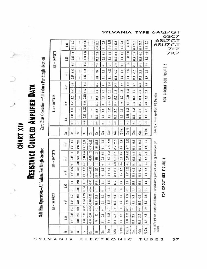
fcc = sqrt(fc1 fc2 (5.15.3) ) Where fcc is the center frequency and fc1 and fc2 are as defined above. If you are working with an AC coupled amplifier, or a band-pass amplifier, use equation 5.15.1 above fcc and equation 5.15.2 below fcc.
In a device such as an audio amplifier the values of fc1 and fc2 usually are easy to measure. For op amps and some very high gain band pass amplifiers the values of fcx are likely to be very difficult to measure so the unity gain frequency is measured and stated in specifications. To calculate the corner frequency from the unity gain frequency we use the following equations.
fc1 = flu AMax positive slope (5.15.4) and
fc2 = fhu / AMax negative slope (5.15.5) where flu is the lower unity gain frequency, fhu is the upper unity gain frequency, fc1 is the lower corner frequency, and fc2 is the upper corner frequency.
Example 5.5.
A DC coupled (op amp) amplifier has a DC gain of 100,000 and a gain-bandwidth product (unity gain frequency) of 3 MHz. What is its gain at (a) 100 kHz, (b) 20 kHz, (c) 1000 Hz and (d) 5 Hz?
Solution:
The Bode diagram for this amplifier would be similar in appearance to the green curve in Figure 5.3 but the values would be different. There are no positive slopes in the diagram and so we apply equation 5.15.5 to find fc2.
fc2 = fhu / AMax = 3 x 10⁶ / 105 = 30 Hz.
(a) Using equation 5.15.1 we have
A = 105 / sqrt((105 / 30)2 + 1) = 30
(b) A = 150
(c) A = 2,999
(d) A = 98,639.
Example 5.6.
An AC coupled amplifier has a lower unity gain frequency of 0.1 Hz and an upper unity gain frequency of 100 MHz. Its mid-band (maximum) gain is 1,000. What is its gain at (a) 5 Hz, (b) 20 Hz, (c) 1 kHz, (d) 20 kHz, (e) 200 kHz and (f) 4 MHz?
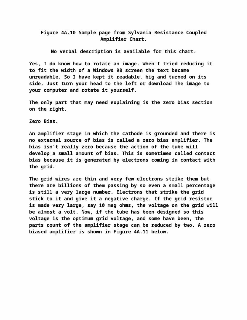
Solution:
The Bode diagram for this amplifier is shown in Figure 5.7. Making a Bode diagram is a good way to avoid mistakes in problems of this kind.
Figure 5.7 Bode Diagram for Example 5.6.
For a verbal description click here.
The first step is to find fc1 and fc2.
fc1 = flu AMax = 0.1 x 1000 = 100 Hz.
fc2 = fhu / AMax = 108 / 1000 = 105 Hz.
In order to decide which equation to use we must split the frequency response curve at the center of the flat portion. The center is the geometric mean of 100 Hz and 100,000 Hz. fcc is given by,
fcc = sqrt(100 x 100,000) = 3.16 kHz
(a), (b), and (c), are all below the center frequency and (d), (e), and (f), are all above it. Therefore we will use equation 5.15.2 for (a), (b), and (c), and 5.15.1 for (d), (e), and (f).
From equation 5.15.2 we have,
(a) A = 49.94,
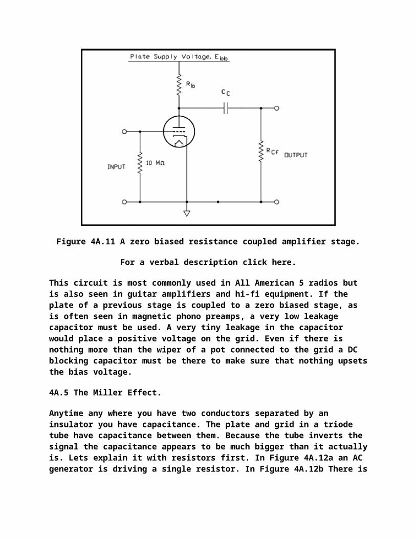
(b) A = 196.1,
(c) A = 995.0
Now changing to equation 5.15.1,
(d) A = 980.6.
(e) A = 447.2,
(f) A = 24.99.
The Feedback Equation with Sloping Gains.
The examples above show how the magnitude of the amplifier gain varies with frequency. In order to make absolutely correct calculations of closed loop gain, taking phase shift into account, we would have to use the j operator. There is no mathematically rigorous way around it. You might suppose that we could use the Pythagorean theorem as we did in our study of RC circuits but the phase shift is not ninety degrees in the region around the corner frequency. The equation that produced the green line in figure 5.7.1 looks like this.
That equation seems to work but it trades off accuracy in one part of the frequency spectrum for inaccuracy in another. A graph will show what's going on.
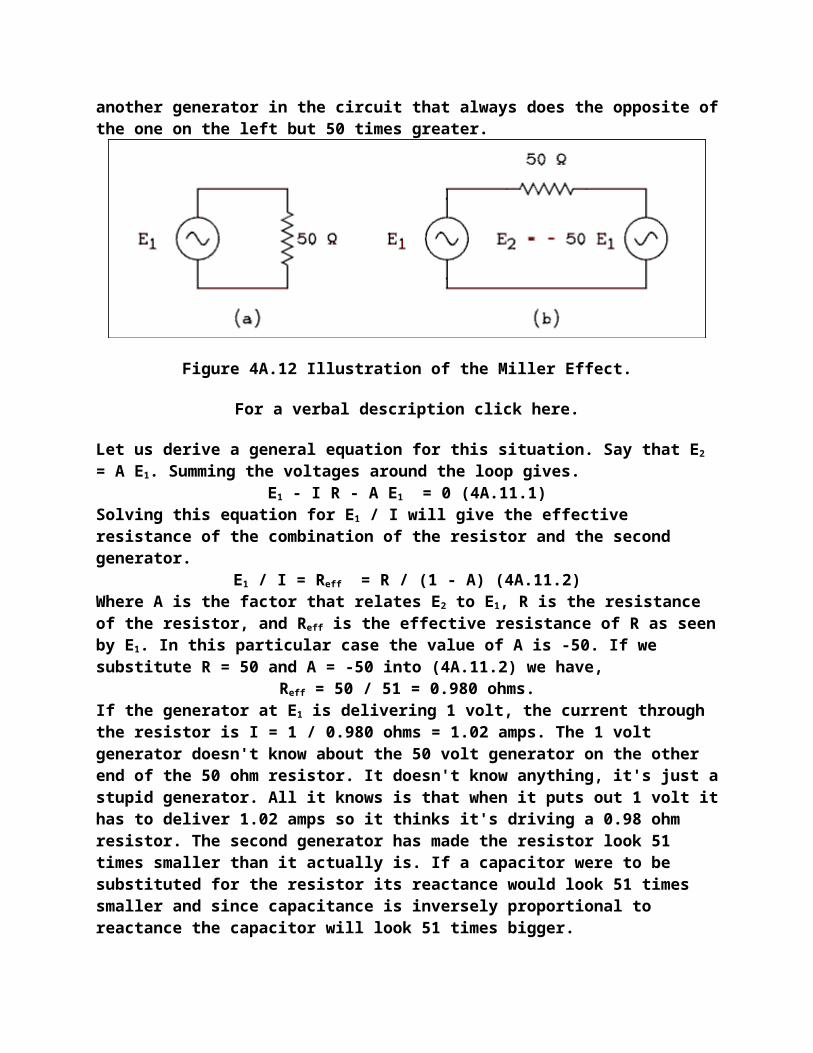
Figure 5.7.1 Curves showing open-loop gain and three calculations of closed-loop gain.
For a verbal description click here.
The graph shows frequency on a log scale versus dB. The numbers along the horizontal axis are the power to which you must raise 10, to obtain the frequency. The scale is from 0.1 to 100,000 Hz. Remember that ten to the 0 power is one. The red curve shows the open loop gain of a DC coupled amplifier with a DC gain of 10,000 and a unity gain bandwidth of 100 kHz. Notice that the gain is down by 3 dB at 10 Hz as it is supposed to be.
The dark blue curve is the gain calculated from equation 5.4. Notice that it is down 6 dB at 100 Hz but it should be 3 dB down.
The green curve is calculated from the equation above. It is correct in this area of the spectrum, being 3 dB down at 100 Hz but the low frequency (DC) part of the curve is off by 1 dB, approximately 10%. As beta is made smaller this error gets worse. For a beta of 0.0001 the DC gain should be 5,000 which is 74 dB. The above equation, which has no number, gives 7,071 which is 77 dB. Such large errors in DC gain calculation cannot be tolerated so the no-number equation will be considered invalid and will not be used.
The equation which produced the light blue line is given below, along with its low frequency companion.
These equations were not so much derived as they were cloodged together to get the right answer. The light blue line behaves the way the real frequency response does. However, equations 5.4.1 and 5.4.2 will not be required in homework or test problems. They are presented for reference only.
Example 5.7.
A beta value of .01 is applied to the amplifier of example 5.5. What is the closed-loop gain at frequencies of (a) 100 kHz, (b) 20 kHz, (c) 1 kHz and (d) 5 Hz?
Solution:
(a) A' = A / (1 + A beta) = 30 / (1 + 30 x 0.01) = 23.08
(b) A' = 60.00
(c) A' = 96.77
(d) A' = 99.90
5.5 Gain Accuracy and Precision.
Amplifiers without feedback have rather unpredictable gains. Transistor parameters vary with temperature and from one transistor to the next. Even if a one-of-a-kind amplifier were designed and constructed, its gain would change with temperature. If a transistor ever had to be replaced the gain would most likely change drastically.
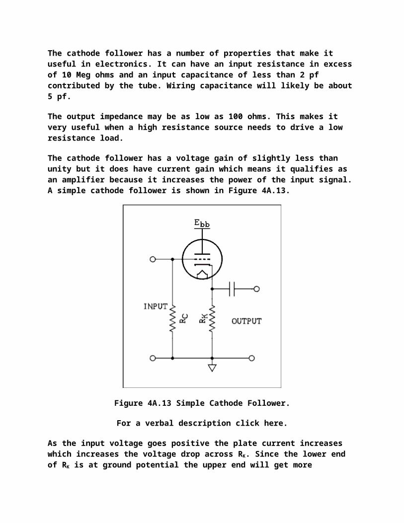
Amplifiers which are used in physics laboratories are involved with measurement of an electrical quantity. A changing gain in a measurement circuit will render the measurement useless. Negative feedback will stabilize the gain of an amplifier. How sensitive the closed-loop gain is to changes in open-loop gain can be determined through the use of calculus.
We will begin with the feedback equation
(5.16) A' = A / (1 + A beta) Using implicit differentiation to take the derivative of A' with respect to A we have,
dA' = ((1 + A beta)dA - A beta dA) / (1 + A beta)2 (5.17) Splitting equation 5.17 into the difference of two quotients gives.
dA' = (1 + A beta) dA / (1 + A beta)2 - A beta dA / (1 + A beta)2 (5.18) Now we will split the right-hand term into the product of two quotients and, at the same time, multiply everything to the right of the equal sign by 1 in the form of A / A and cancel (1 + A beta) in the first term. We now have, dA' = A / (1 + A beta) x dA / A - A / (1 + A beta) x A beta / (1 + A (5.19) beta) x dA / A. The right-hand side of equation 5.16 appears twice in equation 5.19. If we substitute 5.16 into 5.19 we now have
(5.20) dA' = A' x dA / A - A' x A beta / (1 + A beta) x dA / A If we now divide through by A' and factor out the dA / A term we have
(5.21) dA' / A' = dA / A (1 - A beta / (1 + A beta)) Simplifying the term inside the brackets gives,
(5.22) dA' / A' = dA / A x 1 / (1 + A beta) This is where the EE book I used at university stopped. But The equation can be simplified still further. To shorten the notation let us say that E = dA / A and E' = dA' / A'. In this notation we can write,
(5.23) E' = E / (1 + A beta) If we solve equations 5.23 and 5.16 for 1 / (1 + A beta) and set them equal we have.
(5.24) E' / E = A' / A Because E' and E now appear as a ratio it doesn't matter if we express E' and E as fractional changes or percentage changes.
This equation gives us one of the more important benefits of negative feedback, which is to stabilize the gain of an amplifier. Let us illustrate with an example.
Example 5.8.
An amplifier has an open-loop gain of 105 which may vary by as much as plus or minus 30%. The value of beta is 0.010. What is (a) the closed-loop gain, (b) how much is this gain in error referenced to 1 / beta, and (c) what is the percent variation in gain due to changes in open-loop gain?
Solution:
(a) The closed loop gain is
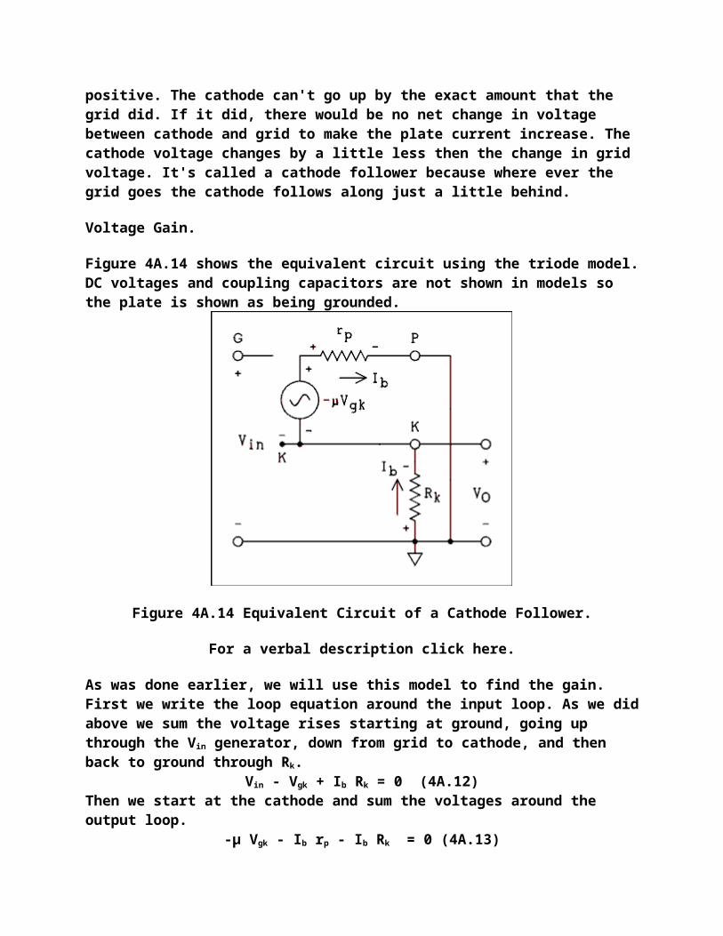
A' = 105 / (1 + 105 x 0.01) = 99.90
(b) Error referenced to 100 is -0.1%
(c) By equation 5.24
E' = E A' / A = 30 x 99.90 / 105 = 0.0300%.
This example shows that when the open-loop gain is very high, it has very little effect on the closed-loop gain. The closed-loop gain is set by beta which in turn is set by the values of two resistors. Resistors can be obtained as very high precision units.
It is often necessary to calculate how much open-loop gain is required or how much closed-loop gain can be obtained for a certain amount of gain error.
Example 5.9.
An amplifier has an open-loop gain of 5,000 which can vary by as much as 35 %. What is the maximum closed- loop gain available if the closed-loop gain variation is not to exceed 2.5 %?
Solution:
Solving equation 5.24 for A' gives,
A' = E' A / E = 2.5% x 5000 / 35% = 357.
5.6 Other Benefits of Negative Feedback.
A fairly obvious question is "If negative feedback reduces the gain, why use it?" In the previous section we have seen that applying negative feedback to an amplifier will control its gain very accurately. That is not the only benefit of negative feedback. Almost any amplifier parameter you care to name is improved by applying negative feedback to it. Any amplifier designer will tell you that gain is the easiest of all parameters to obtain. The standard practice is to design an amplifier with much more gain than is needed and use negative feedback to trade the extra gain for improvement of all of the other parameters of the amplifier.
Frequency Response.
Frequency response is improved by the application of negative feedback. The low frequency limits are moved lower and the high frequency limits are moved higher. For example look at the Bode diagram in Figure 5.8.
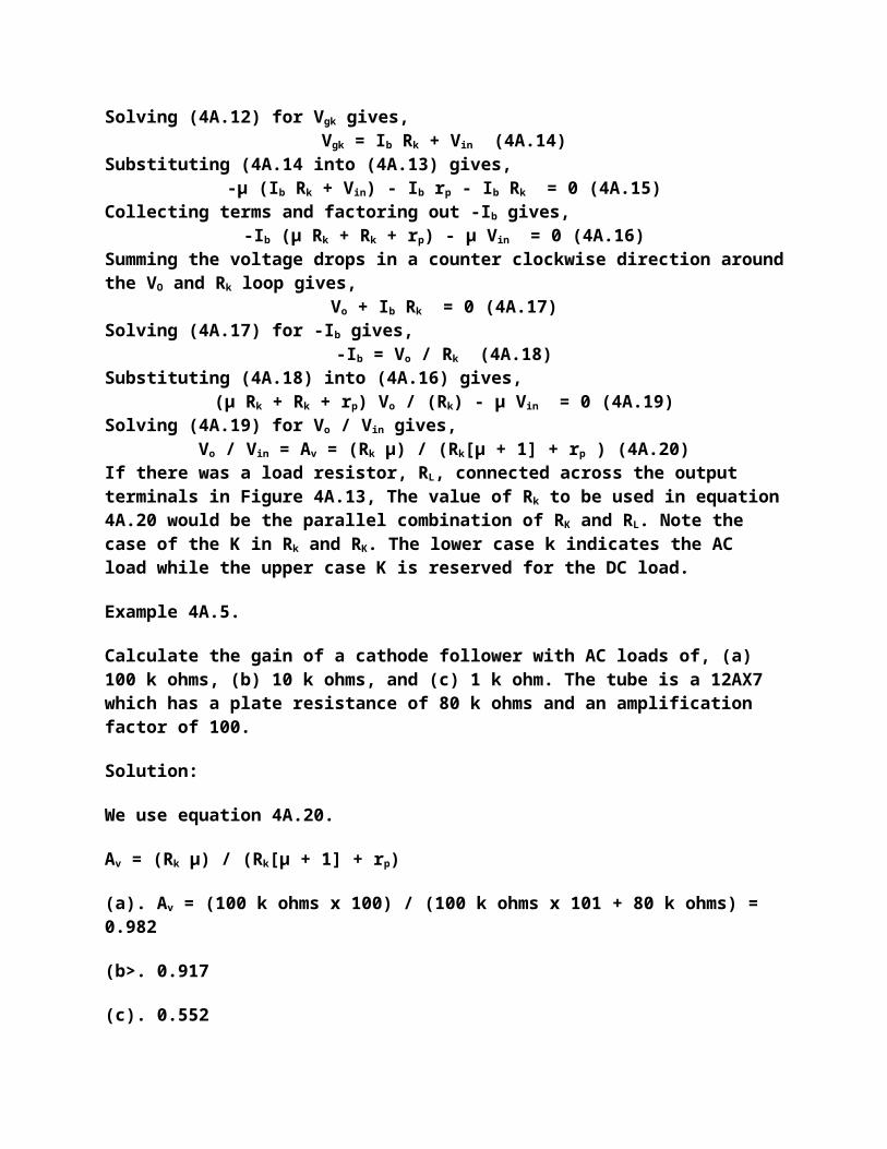
Figure 5.8 Bode Diagram of Closed and Open-loop Gains.
For a verbal description click here.
The frequency response of amplifiers is usually given in terms of the -3 dB points rather than the unity gain points. The open-loop gain of the amplifier whose Bode plot is given in Figure 5.8 has a frequency response of 1,000 to 10,000 hertz. Not exactly hi-fi is it? When negative feedback is applied to reduce the gain to 100, the frequency response becomes 10 Hz to 1 MHz. Quantitatively the improvement of frequency response is given by,
f1' = f1 (5.25) / (1 + A beta) and
f2' = f2 (5.26) (1 + A beta) Where f1 is the lower open-loop -3 dB frequency, f2 is the upper open-loop -3 dB frequency and the primes ' indicate the closed-loop equivalents.
Distortion and Noise.
Distortion is defined as any alteration of the original signal by an electronic circuit. In audio circuits distortion is expressed as a percentage. When an absolutely pure sine wave is introduced at the input of an amplifier, the output consists of the original sine wave plus harmonics of the original sine wave. The total of the harmonics is expressed as a percentage of the original sine wave. This is often called the total harmonic distortion or THD of an amplifier. To a musician, distortion represents an alteration of the reproduced sound. To a physicist, distortion represents nonlinearity and errors in measurements. Distortion and nonlinearity are reduced by the addition of negative feedback to an amplifier as follows. Consider THD to be equivalent to nonlinearity.
(5.27) THD' = THD / (1 + A beta)
Noise is any varying voltage in a place where it is not wanted. It can be periodic as in the case of the 60 Hz line frequency which gets into everything. Noise can be aperiodic or random. Such noise is caused by the thermal agitation of charge carriers in conductors and semiconductors. The amount of noise N is affected by negative feedback as follows.
(5.28) N' = N / (1 + A beta) It should be pointed out that because the signal is also reduced by the factor of 1 / (1 + Abeta) the signal-to-noise ratio is not improved by negative feedback but it isn't made any worse either. The fact that negative feedback is neutral when it comes to signal-to-noise ratio means that the other benefits of negative feedback can be realized without giving up anything really important.
Input and Output Impedance.
The output impedance is lowered by the application of negative feedback by, ZO' = ZO (5.29) / (1 + A beta)
In the case of a noninverting amplifier the input impedance is increased by an amount, ZIN' = ZIN (5.30) (1 + A beta)
The input impedance which is affected is the input impedance of the transistor. Any fixed resistors which are outside of the feedback loop, such as base biasing resistors, will not be affected by the application of feedback.
5.7 Some Practical Circuits.
From time to time in this text, laboratory tested circuits will be presented. A circuit which actually works can illustrate a principle as well as one which looks as if it might work but probably will not. The latter kind of circuits are what are normally presented in electronics texts.
It is not intended that you should memorize these circuits; they are given for possible future reference. Some day if you are in graduate school or a job and you need a circuit to accomplish some task, you may just find one here. Where practical, hints will be given on how changes may be made to the circuit to help you to adapt it to your particular situation.
The circuit of Figure 5.9 is a two-stage noninverting amplifier with feedback. The feedback is applied from the output, through the voltage divider consisting of R9 and the parallel combination of R10 and R4. For this circuit,
beta = R4 R10 / (R4 R10 + R9 (R4 + R10 (5.31) ) C2 is required because the tap on the voltage divider and the emitter of Q1 are at different DC voltage levels.
The idea of applying a signal to the emitter of a transistor may seem strange. There is an amplifier configuration (not discussed) which is known as a common base or grounded base amplifier. In such a configuration the signal is applied at the emitter and taken out at the collector. Such an amplifier does not invert the input signal. Applying a positive-going
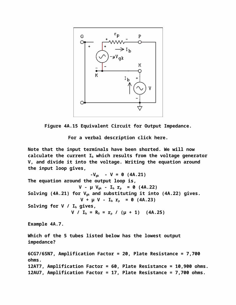
signal to the emitter is the same as applying a negative-going signal to the base. Therefore, if a signal applied to the base is inverted, a signal applied to the emitter is not inverted.
Figure 5.9 Laboratory Tested Circuit. Gain = 47, FrequencyResponse is from 35 Hz to 600 kHz +0 -3 dB, Input Impedance
is 9 k ohms, Output Impedance is 700 ohms, VCC is 12 volts.The gain may be altered by changing the value of R9.
The transistors are 2N3904.
For a verbal description click here.
The amplifier of Figure 5.9 has two BJT stages. The signal which is applied to the base of Q1 is inverted by that stage and applied to the base of Q2 where it is inverted again. Two inversions make a noninversion and, therefore, the base of Q1 is a noninverting input. A signal applied to the emitter of Q1 appears at its collector without being inverted. When this signal is passed through the Q2 stage it is inverted. Therefore, the emitter of Q1 is an inverting input. If negative feedback is to truly be negative, it must be applied to an inverting input.
The circuit of Figure 5.9 contains a large number of resistors and capacitors because each transistor is individually biased. The circuit of Figure 5.10 eliminates the DC blocking capacitor between Q1 and Q2 and the biasing network in the base of Q2. A DC voltage exists at the collector of Q1 and a DC voltage is required at the base of Q2. The designer's trick is
to make the two voltages equal and then eliminate the capacitor and biasing resistors. The base of Q2 gets its bias from the collector of Q1.
Figure 5.10 Laboratory Tested Circuit. Gain = 85,frequency Response is from 4 Hz to 230 kHz +0 -3 dB,
input Impedance is 53 k ohms, output Impedance is 580 ohms, Gain may be adjusted by changing R7.
For a verbal description click here.
This circuit is especially interesting because it has two feedback paths. One is from the emitter of Q2 to the base of Q1 and the other is from the collector of Q2 (the output) to the emitter of Q1. Capacitor C2 filters out the AC signal at the emitter of Q2 and so the feedback path from the emitter of Q2 to the base of Q1 is DC only. Because Q2 gets its base bias from the collector of Q1, any change in the operating point of Q1 will be amplified and passed to Q2. The DC feedback path provides operating point stability for both stages.
If the emitter current of Q2 tries to increase, for whatever reason, the base bias on Q1 will be increased through the voltage divider consisting of R1 and R2. The increased bias on Q1 will cause its collector current to increase which pulls down its collector voltage. Since the base of Q2 is tied to the collector of Q1 the base bias on Q2 will be decreased, thus mostly canceling the increase in emitter current.
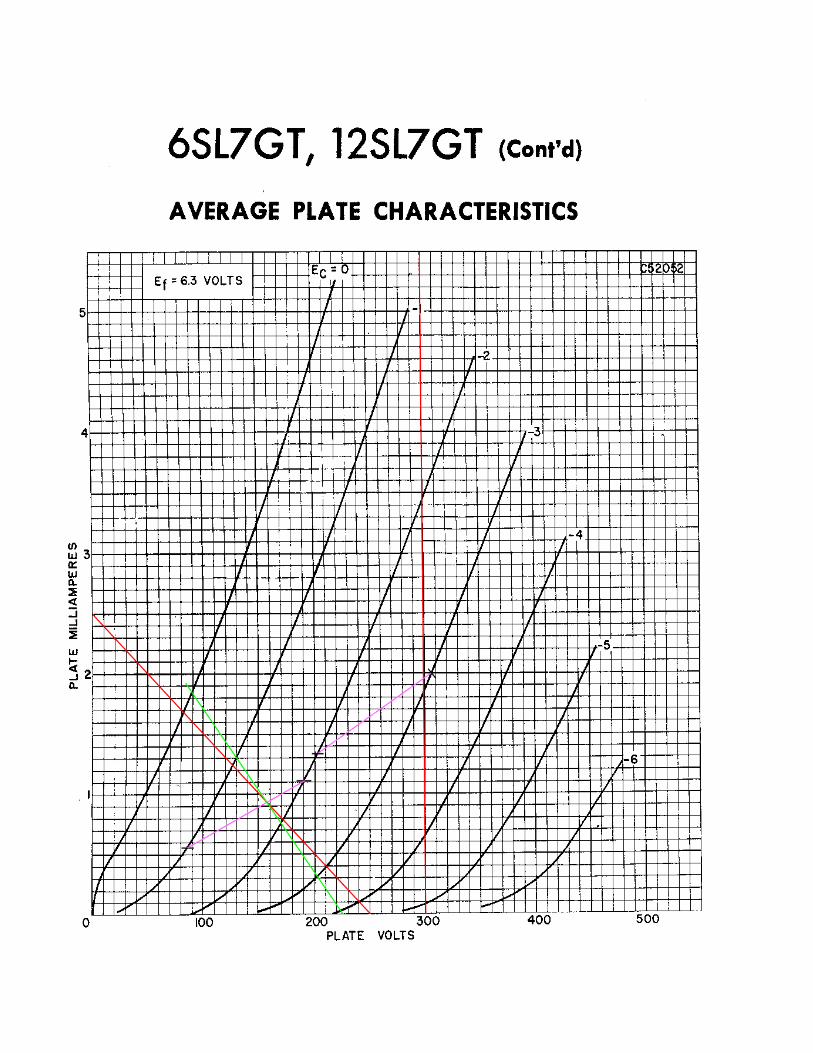
The AC gain is set by the AC feedback path which is from the output, through the voltage divider consisting of R7 and R4 to the emitter of Q1. In this case,
beta = R2 / (R2 + R7 (5.32) ). The value of R2 cannot be changed as this will upset the DC operating point of both transistors. R7 may be adjusted to set the gain to the desired value.
Figure 5.11 shows another variation on the same theme. The advantage of this circuit over Figure 5.10 is that the output voltage swing can be almost equal to VCC. In the case of Figure 5.10 the base of Q2 is at the same potential as the collector of Q1, and so VCE + VRE of Q1 is not available for output voltage swing. The circuit of Figure 5.11 overcomes this by using a PNP and an NPN transistor. The emitter of Q2 is at VCC and the output voltage can almost swing from ground to VCC.
Figure 5.11 Laboratory Tested Circuit. Gain = 24, Frequency Response is from 3 Hz to 1 MHz +0 -3 dB, Input Impedance is 16.5 k ohms, Output Impedance is
332 ohms, VCC is 12 volts. The gain may be altered by changing the value of R7.
For a verbal description click here.
The voltage divider consisting of R1 and R2 provides a constant bias for the base of Q1. For DC, 1/2 of the output is fed back to the emitter of Q1 for operating point stability. R4, R5
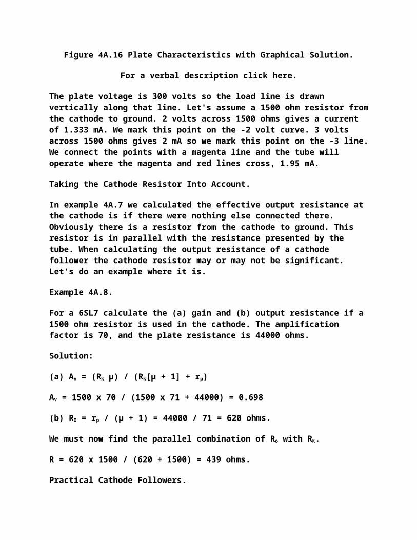
and R6 provide the DC feedback to the emitter of Q1. R7 and C2 combine to reduce the amount of AC feedback which will raise the AC gain of the amplifier. If R7 is shorted out, the amplifier will provide its full open- loop gain for AC. If R7 and C2 are removed from the circuit, the gain will be 2 for both AC and DC.
beta = R6 R7 / ((R4 + R6 + R7)(R5 + R6) - R62 ) (5.33)
If the circuit is to be used as a DC amplifier, capacitors C1 and C3 would have to be removed from the input and output. The circuit as given would introduce a DC offset to the signal. The resistor values probably could be adjusted to reduce the offset to near zero.
Here is the circuit of a vacuum tube gain block. Gain blocks usually consist of two triodes with feedback from output plate to input triode cathode to diminish distortion to a very low level and tightly control the value of the gain. Here is a circuit I developed that will give a fairly wide range of gain at very low levels of distortion.
Figure 5.11.1 Vacuum Tube Gain Block.
For a verbal description click here.
This circuit has a lot of open loop gain which is traded off for low distortion. The gain may be changed by changing the cathode resistor, Rk, in the first triode. Changing this resistor has a very small effect on the operating point of either triode. The numbers are given in the table below.
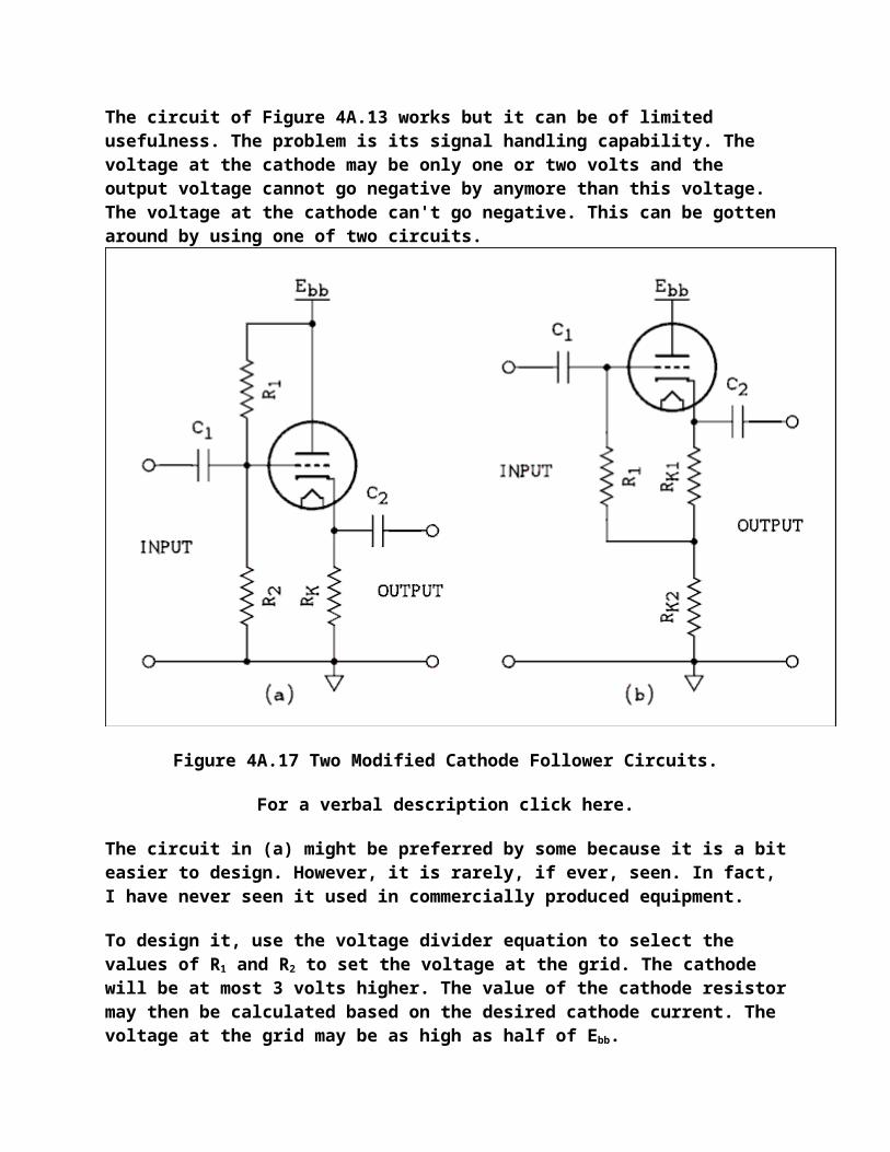
Cathode Resistor, Rk. Gain. Distortion. Output Voltage.
36 k ohms. 6.67 0.035%. 10 v.
27 k ohms. 8.47 0.04%. 10 v.
22 k ohms. 10.1 0.045%. 10 v.
9.1 k ohms. 21.7 0.045%. 10 v.
5.1 k ohms. 33.6 0.060%. 10 v.
The value of beta for this circuit is given by, beta = (Rk + 1100) / (Rf + Rk (5.33.1) + 1100)
Where Rk and Rf are as labeled in the schematic above.
The feedback is DC coupled, not through a capacitor, from the plate of the second triode to the cathode of the first.
The 220 k ohm resistor makes up most of the load for the second triode which is where most of the distortion occurs. I don't recommend changing the value of Rf because it effects the operating point of the second triode. If this resistor is changed the cathode resistor in the second triode will have to be readjusted for minimum distortion.
5.8 Positive Feedback, Oscillators.
It has been said that if a phase reversal slips into a negative feedback circuit, the amplifier will oscillate. There are circuits in which the feedback is deliberately made positive so as to generate an AC signal of known and constant frequency. Such circuits are known as oscillators.
If we reverse the sign of the feedback the feedback equation becomes,
(5.34) A' = A / (1 - A beta) If A is less than 1 / beta the gain of the amplifier is increased over its open-loop value but it will still work as an amplifier. If A = 1 / beta the gain becomes infinite and the amplifier will provide its own input signal and will produce an output without any input. Mathematically if A is greater than 1 / beta the amplifier will oscillate and the amplitude of the oscillations will continue to build up and approach infinity. In the physical world amplifiers do not work this way. The amplitude will build up until the amplifier begins to saturate which has the effect of reducing the open-loop gain. The gain will be reduced until A = 1 / beta.
Multivibrator.
The circuit of Figure 5.12 is at first glance two common emitter amplifiers, each one with its collector coupled to the other's base. Starting at one particular point and moving around the loop once, there are two 180 degree phase shifts which gives a total of 360 degrees, which is the same as a 0 degree phase shift. In actuality the transistors are acting as switches instead of amplifiers.
Figure 5.12 Laboratory Tested Circuit. Oscillationfrequency is 80 Hz, VCC may be as low as 1.5 v, Waveform
is approximately square, Amplitude = (VCC - 0.1) v P-P.
For a verbal description click here.
Let us start by assuming that Q1 is off and Q2 is on. The voltage at the collector of Q1 will be VCC and the voltage at the base will be negative because of remaining charge on C2. The voltage at the collector of Q2 will be approximately zero volts and the voltage at the base will be +0.6 volts. The charge on C1 will be equal to VCC - 0.6 v with the left-hand plate positive. C2 once had a charge of VCC - 0.6 v with the right-hand plate positive. C2 is now discharging through R3 causing the negative voltage at the base of Q1 to be headed in the direction of VCC. When the base voltage of Q1 reaches +0.6 volts, Q1 begins to conduct and its collector voltage begins to fall. This falling voltage is coupled through C1 to the base of Q2 which turns it off. When Q2 turns off, its collector voltage goes up and that change causes C2 to be charged through the base of Q1, turning it on very hard. Q1 is now on and Q2 is now off. C1 has a charge of VCC - 0.6 v with the left-hand plate positive. Because the left-hand end of C1 is clamped to ground by Q1 the base of Q2 is negative, insuring that it is off. C1 begins to discharge and the cycle keeps repeating with each transistor switching alternatively on and off.
If R2 = R3 = R and C1 = C2 = C then the frequency of oscillation is given by,
(5.35) f = 1 / (1.2 R C)
The frequency of oscillation is relatively insensitive to the power supply voltage.
Circuits You May Find in Other Texts.
A good example of a circuit you may find in other electronics texts is the Wien bridge oscillator. This is a sine wave oscillator which, if properly designed, is capable of generating very pure sine waves. Back in the vacuum tube days this circuit used a tungsten lamp as a gain regulating element. The circuit was fairly simple and it worked quite well. Modern Wien bridge designs which employ a lamp do not work very well. A high-quality Wien bridge circuit is too complex to be presented in a text of this level. The simple circuits you may see in other texts are not laboratory tested and will likely not work. The writer refuses to waste space printing circuits which won't work.
The Phase-shift Oscillator.
Figure 5.13 Laboratory Tested Circuit. This circuit operatesfrom 12 volts and with the given values will oscillate at
approximately 200 Hz. Its usable frequency range is from 5Hz to 20 kHz. For best waveform use the pot to adjust the
output amplitude to 2.25 volts RMS. The waveform is a prettygood sine wave.
For a verbal description click here.
The phase-shift oscillator works by using the phase- shift of an RC circuit. Oscillation requires a net phase- shift around the feedback path of zero degrees. The amplifier stage in Figure 5.13 provides a phase-shift of 180 degrees. Three cascaded high-pass filters are used to provide the additional 180 degrees of phase-shift. One RC filter will provide a maximum
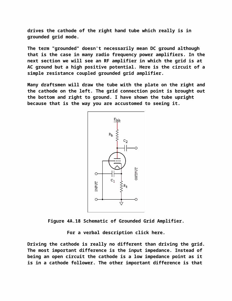
of 90 degrees of phase-shift and you might assume that two such circuits would be enough. The phase- shift of a high-pass filter reaches 90 degrees at infinitesimally low frequencies. At such low frequencies the attenuation is approaching infinity. When three filters are used each filter is required to provide a phase-shift of only 180 degrees / 3 = 60 degrees. Because the next filter loads the previous one each section does not provide exactly 60 degrees but the average is 60 degrees per section. Under these conditions the attenuation is finite and the circuit will work.
There is only one frequency at which the total phase- shift is 180 degrees and it is given by,
(5.36) f = 1 / (2 Pi sqrt(6) R C). The attenuation of the circuit at this frequency is 1/29 and so the amplifier must have a gain of at least 29. The gain of the amplifier in Figure 5.13 may be set to 29 by means of the potentiometer. If the gain falls below 29 the circuit will stop oscillating. If the gain is higher than 29 the waveform will have a bit of distortion but the circuit will work reliably.
Quartz Crystal Oscillator.
Quartz is a Piezoelectric material when properly cut. The meaning of Piezoelectric is that there is an interchange between applied electric field and mechanical deformation. If the cut piece of quartz crystal is mechanically deformed, an electric field will be developed across the quartz. If an electric field is applied to a quartz plate, the plate will be mechanically deformed.
Because mechanical waves propagate through the quartz plate at a very high velocity, a thin plate of quartz will have a very high mechanical resonant frequency (roughly from 10 kHz to 100 MHz). The Piezoelectric effect allows this mechanical resonance to be transformed into an electrical resonance.
The quartz crystal behaves as if it were an LC resonant circuit. Crystals have two major advantages over LC circuits. They are 1) the quartz crystal is usually smaller than an LC circuit tuned to the same frequency and 2) the crystal has a much higher Q than an LC circuit tuned to the same frequency. The highest achievable Q values for an LC circuit are 250, although 100 is more typical. Crystal Q values range from 1,000 to 10,000. The only disadvantage of a quartz crystal is that its frequency cannot be adjusted once it leaves the factory.
When a quartz crystal is used as the frequency- determining element of an oscillator (as opposed to an LC circuit), the oscillator frequency is much more accurate and stable. The much higher Q of the crystal is what makes the oscillator frequency so much more stable.
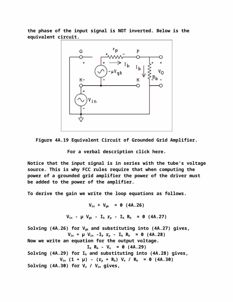
Figure 5.14 Laboratory Tested Circuit. This is a quartzcrystal oscillator with a frequency of 2 MHz and an
output suitable for driving one TTL logic load.
For a verbal description click here.
Figure 5.14 shows the diagram of a 2 MHz quartz crystal oscillator. The 7 to 45 pf trimmer capacitor may be used to adjust the frequency over a very small range, typically 0.05% of the crystal frequency. The JFET section is the oscillator circuit. This section could be constructed alone and the output taken from the source of the FET. The BJT portion operates as a switch and it is turned on and off by the AC signal from the oscillator portion. The entire circuit should work perfectly using a 1 MHz crystal. The oscillator section has been tested using a 10 MHz crystal but the BJT switch has not.
If you apply what you know about switching circuits you will find that the BJT is neither fully on or fully off. That is desirable in this application because the AC signal from the oscillator will drive the switch alternately on and off. If the switch were set fully off, the AC signal from the oscillator might not have enough amplitude to turn it on.
5.9 Problems.
1. An amplifier has an open-loop gain of 300 and a beta of 0.01. What is its closed-loop gain?
2. A noninverting amplifier has an open-loop gain of 8. R1 = R2 = 12 k ohms. What is the closed-loop gain of this amplifier?
3. An inverting amplifier has an open-loop gain of 8. R1 = R2 = 12 k ohms. What is the closed-loop gain of this amplifier?
4. A noninverting amplifier has an open-loop gain of 1,000. R1 = 10 k ohms and R2 = 40 k ohms. What is the closed-loop gain of this amplifier?
5. An inverting amplifier has an open-loop gain of 1,000. R1 = 10 k ohms and R2 = 40 k ohms. What is the closed-loop gain of this amplifier?
6. An amplifier which has a Bode plot similar to that of Figure 5.4 has a DC gain of 75,000 and a gain-bandwidth product of 1.5 MHz. What is its gain at frequencies of (a) 100 kHz, (b) 20 kHz, (c) 1 kHz, (d) 20 Hz, and (e) 5 Hz?
7. If negative feedback is applied to the amplifier of problem 6 and the value of beta is 0.013333, what is the closed-loop gain at frequencies of (a) 100 kHz, (b) 20 kHz, (c) 1 kHz, (d) 20 Hz, and (e) 5 Hz?
8. An amplifier which has a Bode plot similar to that of Figure 5.5 has a lower unity gain frequency of 0.5 Hz, an upper unity gain frequency of 10 MHz and a maximum gain of 300. What is its gain at frequencies of (a) 5 Hz, (b) 20 Hz, (c) 200 Hz, (d) 1 kHz, (e) 20 kHz (f) 50 kHz, and (g) 2 MHz?
9. If negative feedback is applied to the amplifier of problem 8 and the value of beta is 0.025, what is the closed-loop gain at frequencies of (a) 5 Hz, (b) 20 Hz, (c) 200 Hz, (d) 1 kHz, (e) 20 kHz, (f) 50 kHz and (g) 2 MHz?
10. An amplifier is required to have a gain stability of 0.5%. The open-loop amplifier has a gain stability of 20%. If the closed-loop gain is to be 200, what must be the minimum open-loop gain of the amplifier?
11. An amplifier has a closed-loop gain of 1,000 and an open-loop gain of 100,000 plus or minus 50%. What is the closed- loop gain error?
12. An amplifier has an open-loop gain of 300,000 plus or minus 40%. What is the maximum closed-loop gain available if the error in the closed-loop gain is not to exceed plus or minus 1%?
13. What is the calculated value of beta of Figure 5.9? 14. In Figure 5.9 if the open-loop gain is 280, what is the closed-loop gain? 15. In Figure 5.12 if resistor values are as given, what must the values of C1 and C2 be to
give an oscillation frequency of 60 Hz? 16. In Figure 5.13 if all capacitors marked C are 0.001 uf, what must be the value of the
resistors R to give an oscillation frequency of 440 Hz? 17. In Figure 5.14 if there were no AC signal from the oscillator, what would be the
value of VCE of the BJT? Assume beta = 100.
5.10 Answers to Problems.
1. 75. 2. 1.6. 3. -0.8. 4. 4.975. 5. -3.98. 6. (a) 15.0, (b) 75.0, (c) 1500, (d) 53,033, (e) 72,761. 7. (a) 12.50, (b) 37.50, (c) 71.43, (d) 74.89, (e) 74.92.
Note. These calculations are correct not just close.If you didn't hit the numbers on the nose,you must have done something wrong.
8. fc1 = 150 Hz, fc2 = 33,333 Hz, fcc = 2,236 Hz.(a) 9.994, (b) 39.65, (c) 240.0, (d) 296.7, (e) 257.2, (f) 166.4, (g) 4.999.
9. (a) 7.996, (b) 19.91, (c) 34.28, (d) 35.25, (e) 34.62, (f) 32.25, (g) 4.444. 10. 8000. 11. 0.5%. 12. 7,500. 13. 0.01799. 14. 46.38. 15. 0.13 microfarad. 16. 148 k ohms. 17. 1.48 volts.
This page copyright © Max Robinson. All rights reserved.
The Operational Amplifier. Chapter 6
Op Amp Behavior. 6.1 Equations of the Op Amp. 6.2 The Unity-Gain Buffer Amplifier. 6.3 The Noninverting Amplifier. 6.4 The Inverting Amplifier. 6.5 The Summing Amplifier. 6.6 The Integrating Amplifier. 6.7 Single Power Supply Operation. 6.8 Understanding Op Amp 6.9 Specifications.6.10 Problems.6.11 Answers to Problems.
Chapter 6The Operational Amplifier.
The operational amplifier began life as a component in an analog computer. For those who have never heard of an analog computer, it is (was) a computer in which the magnitude and sign of voltages were used to represent physical quantities. For example, one voltage might represent the velocity of a falling object, another voltage the acceleration and another voltage might represent the frictional drag of the air on the object. If you know about analog computers you think of them as being vacuum tube monstrosities but that is because of the age in which they were developed and used. If they were still in use today they would be reduced in size to desktop or even smaller just as their more successful digital brothers have.
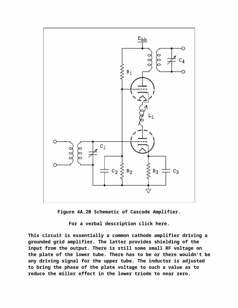
The operational amplifier (op amp) is so called because in its original application it was used to perform mathematical operations. The two operations it was best at were addition and integration. Op amps are still used for these purposes but they have found many other applications in modern electronics.
6.1 Op Amp Behavior.
The op amp has been reduced from its original vacuum tube size of a cubic foot or larger to an 8 pin integrated circuit. There are several hundred different type numbers, each having its own particular and sometimes subtle difference from others. The internal circuitry of these ICs is not terribly important to us. IC manufacturers do not often give the internal circuit diagrams of their ICs. Op amps are among the few exceptions to this rule.
The circuits are quite complex, the 741 op amp has 20 transistors in it. The curious student is referred to instructional books and data books devoted exclusively to op amps. There are many such books available.
Op amps are usually treated as 5 terminal devices. In the following pages they will be treated as just another component the same as a transistor is a component.
Electrical Connections.
The op amp has 5 basic electrical connections. They are inverting input, noninverting input, output, positive power supply and negative power supply. While there is no ground per se, ground is established by the power supply. Employing the theorem which states that "one picture is worth a thousand words" refer to Figure 6.1. The power supplies are replaced by batteries to make it clear how the power supplies are connected. Sometimes an op amp may be operated from a single power supply but most of the time they are operated as shown in Figure 6.1.
Except for section 6.8 you will not again see the power supply connections to an op amp. The power supply connections are always there; they are usually not shown on schematic diagrams. The op amp will not work without power supply connections. If you see a diagram which does not show power supply connections and you assume that it is not necessary to connect a power supply, you will be in error. The op amp will not work without power supply connections. They are always assumed if not shown.
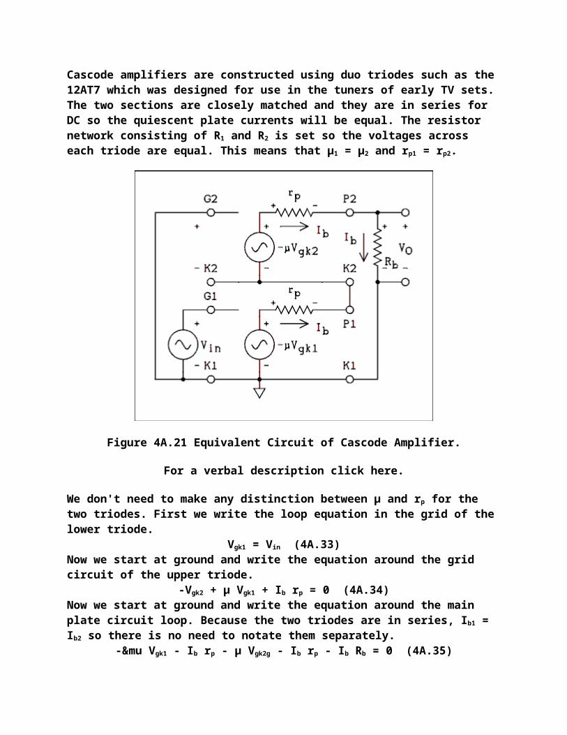
Figure 6.1 Operational Amplifier Showing Power Supply Connections.
For a verbal description click here.
The two inputs must be at a voltage which is between the negative and positive power supplies. To force the voltage of either or both inputs higher than V+ (the positive power supply) or lower than V- (the negative power supply) may destroy the op amp. (There are some special purpose op amps which have been designed to permit the inputs to be at potentials outside of the power supplies. If you have a need to set the inputs outside of the power supplies, you should consult a data book to find such an op amp.)
Many op amps have inputs for adjusting the offset voltage to zero. When the voltage at the two inputs is exactly equal the output should be zero but it is not. The amount by which the input voltage must be different to bring the output to zero is the offset voltage.
The Differential Inputs.
If the inverting input is tied to ground and a variable DC voltage is applied to the noninverting input the output will go with the sign of the noninverting input. If the voltage at the noninverting input is positive, the output is positive and if the voltage at the noninverting input is negative, the output is negative.
Now we will disconnect the inverting input from ground and connect the noninverting input to ground. The variable DC voltage will be applied to the inverting input. When the voltage at the inverting input is positive, the output voltage is negative. When the voltage at the inverting input is negative, the output voltage is positive. Thus you can see why the inputs have been named as they have.
Theoretically, if both inputs are connected together, the output voltage is zero. The offset adjustments can be used to adjust the output to zero, but there is a little more to it than that. If the two inputs (tied together) are made positive or negative, the output voltage will not change. But that's only in theory.
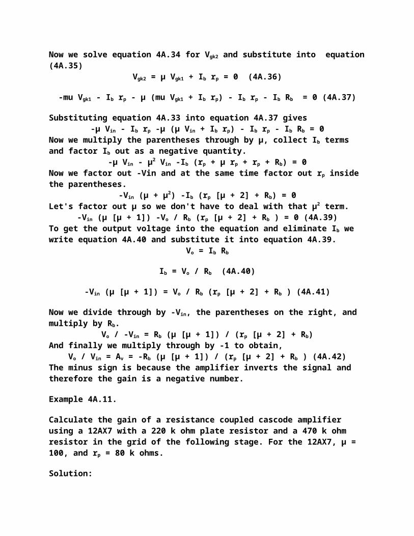
In practical op amps the output voltage will change a little when the two inputs have the same voltage applied to them. A voltage which is applied to both inputs simultaneously is called a common mode voltage. A voltage which is applied between the two inputs is called the normal mode voltage or differential voltage.
The normal mode gain is defined as the ratio of output voltage to the differential input voltage.
ANM = VO / Vd (6.1) Where VO is the output voltage and Vd is the voltage difference between the two inputs. The common mode gain is defined as the ratio of the output voltage to the common mode input voltage.
ACM = VO / VCM (6.2) Where VCM is the voltage applied to both inputs together. The common mode rejection ratio is defined as the ratio of the normal mode gain to the common mode gain.
CMRR = ANM / ACM (6.3) The common mode rejection ratio (CMRR) is usually expressed in dB. The typical value for the 741 type op amp is given as 90 dB.
Example 6.1.
An op amp has had its offset adjusted to zero. Its inverting input is at +3.001 v and its noninverting input is at +3.000 v. Will its output be positive or negative?
Solution:
The noninverting input is negative with respect to the inverting input; therefore, the output will be negative.
Example 6.2.
An op amp has had its offset adjusted to zero. Its inverting input is at -5.001 v and its noninverting input is at -5.000 v. Will its output be positive or negative?
Solution:
The noninverting input is positive with respect to the inverting input; therefore, the output will be positive.
Example 6.3.
When the normal mode voltage is changed by 25 uv the output changes by 5 volts. When the common mode voltage is changed by 1 volt the output voltage changes by 6.325 volts. (a) What is the CMRR? (b) Express the CMRR in dB.
Solution:
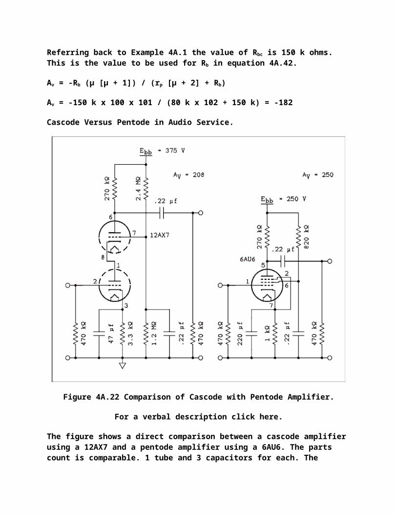
The normal mode gain is 5 v / 25 uv = 200,000. The common mode gain is 6.325 v / 1 v = 6.325. (a) The CMRR is 200,000 / 6.325 = 31620. (b) The CMRR expressed in dB is 20 LOG (31620) = 90 dB.
6.2 Equations of the Op Amp.
The equation of the op amp is based on an approximation, albeit a very good one. Let us restate the feedback equation.
A' = A / (1 + A beta) (6.4) Now we will find the limit as A approaches infinity. If we divide both numerator and denominator by A we have
A' = 1 / (1/A + beta) (6.5) As A approaches infinity, the 1/A term goes to zero leaving
Limit as A approaches infinity of A' = 1 / beta (6.6) Thus, the gain of an op amp with feedback applied is given by
A' = 1 / beta (6.7) While equation 6.7 is a very good approximation in most cases it should not be taken as gospel.
Example 6.4.
An op amp has a DC gain of 100,000 and a unity gain bandwidth of 1 MHz. If feedback is applied to the op amp with a beta value of 0.05, what is the exact closed-loop gain at (a) DC, (b) 1 kHz, (c) 20 kHz, and (d) 100 kHz?
Solution:
From equation 5.15.5 the corner frequency is,
fc2 = fhu / AMax
Where fc2 is the corner frequency, fhu is the upper unity gain frequency, and AMax is the DC gain.
fc2 = 1 MHz / 100,000 = 10 Hz.
(a) Using equation 6.4,
A' = A / (1 + A beta) = 100,000 / (1 + 100,000 x 0.05) = 19.9960
(b) Using equation 5.4.1
A' = ADC / sqrt([f / fc2]2 + [1 + ADC beta]2)
A' = 100,000 / sqrt([1,000 / 10]2 + [1 + 100,000 x 0.05]2) = 19.9920
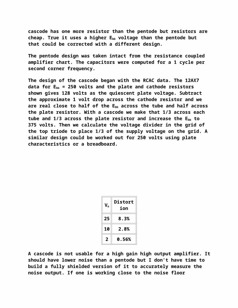
(c) and (d) also use equation 5.4.1.
(c) A' = 18.5663
(d) A' = 8.94391
Example 6.5.
For the conditions of example 6.4 calculate the percent error of gain using 1/beta as the standard of comparisons at (a) DC, (b) 1 kHz, (c) 20 kHz, and (d) 100 kHz.
Solution:
Since 1/beta = 20.00000 the errors are as follows:
(a) -0.020%, (b) -0.040%, (c) -7.1685%, (d) -55.2805%.
As can be seen from these examples the 1/beta approximation is very good at DC and low frequencies but somewhere between 1 and 20 kHz the error crosses over the 2% line. If it is desired to know the exact gain at high audio frequencies equation 5.4.1 must be used rather than 6.4 or 1/beta.
6.3 The Unity-gain Buffer Amplifier.
The definition of a buffer amplifier is an amplifier which will isolate a load from a source. Such isolation usually requires that the buffer amplifier have a very high input impedance. The output impedance may either be very low or matched to the load impedance. A buffer often has unity voltage gain although this is not a requirement under the definition.
A unity gain buffer has a voltage gain of unity as the name implies. The value of beta is set at unity by feeding back all of the output voltage to the inverting input. The circuit of Figure 6.2 is of a unity gain buffer.
Figure 6.2 Unity Voltage Gain Buffer Amplifier.
For a verbal description click here.
An op amp works by adjusting its output so that the two inputs are at the same potential. (The error due to finite op amp gain is quite small.) Because the output and the inverting input are connected together the output voltage will be the same as the inverting input voltage. Suppose that the input voltage is 0 volts and that the voltage is suddenly changed to +2 volts. Since the signal is applied to the noninverting input, for an instant of time the noninverting input will be positive with respect to the inverting input. This will cause the output to go positive. When the inverting input voltage becomes +2 volts the output will stop changing. Should the output voltage overshoot +2 volts and become higher, the output would be urged in the negative direction thus correcting the overshoot. A properly compensated op amp will not overshoot in the first place.
The voltage at the output cannot become 2.000000000000 volts. If it did the differential input voltage would be zero and the output would be zero. Since the output voltage is finite, there must be a finite difference in voltage between the noninverting input and the inverting input. That small but finite difference is caused by the finite open-loop gain of the op amp. Because the open-loop gain of the op amp is very large, the error is very small.
The percent error is,
% error = 100% x (Measured - Reference) / Reference (6.8) If we substitute A / (1 + A beta) for "Measured" and 1/beta for "Reference" in equation 6.8 and get some more algebraic exercise we have
% error = -100% / (1 + A beta) (6.9) In the case of the unity-gain buffer the value of beta is 1.0000000000; therefore, the % error becomes 100% / (A + 1).
Example 6.6.
Calculate the gain error of a unity-gain buffer if the op amp has an open-loop gain of (a) 200,000; (b) 20,000; (c) 1,000; and (d) 20?
Solution:
The % error is (a) -100% / (1 + 200,000) = -0.0004999975%, (b) -0.00499975%, (c) -0.0999%, (d) -4.7619%. The closed-loop input and output impedances of the unity-gain buffer are,
ZIN' = ZIN (1 + A beta) (6.10) And
ZO' = ZO / (1 + A beta) (6.11) The open-loop input and output impedances must be obtained from an IC data-book. Because beta is unity and the open-loop gain is very large, the output impedance is very low and the input impedance is very high.
Often it is desired to calculate the input and/or output impedance at higher frequencies where the gain is less than the DC gain. Equations 6.10 and 6.11 may be used but the value of A must be the gain at the frequency being considered, not the gain at DC. This gain can be obtained from equation 5.15.1 which is repeated below.
Where A is the gain at any frequency, ADC is the DC gain of the amplifier, f is the frequency at which the gain is desired, and fc2 is calculated from equation 5.15.5 which is repeated below.
fc2 = fhu / ADC (6.11.2) Where fhu is the unity gain bandwidth or gain bandwidth product of the amplifier.
Example 6.7.
Determine the minimum input impedance and the maximum output impedance of a unity-gain buffer employing a type 741 op amp. The data book gives the minimum input resistance of the 741 as 0.3 M ohms, a typical output resistance of 75 ohms and a minimum gain of 20,000. The typical gain is given as 200,000.
Solution:
The minimum gain is given as 20,000. The typical gain is given as 200,000 but as the question asks for the minimum input impedance and maximum output impedance, the minimum gain should be used.
ZIN = 0.3 M ohms x 20,000 = 6 G ohms,
The output impedance is, ZO = 75 / 20,000 = 3.75 milli ohms.
The resistance of the printed circuitboard traces will be greater than the output resistance of the amplifier. Note also that this is a worst case. If the typical gain of 200,000 had been used, the input impedance would be 60 G ohms and the output impedance 0.375 m ohms.
6.4 The Noninverting Amplifier.
Figure 6.3 Noninverting Amplifier.
For a verbal description click here.
The circuit of a noninverting amplifier is given in Figure 6.3. As we saw in the previous chapter the value of beta for this amplifier is given by,
beta = R1 / (R1 + R2 ) (6.12) The approximation for the closed-loop gain is given by equation 6.7. If the gain error is large, equation 6.4 should be used to calculate the exact gain. The gain error is given by equation 6.9. The input and output impedances are given by equations 6.10 and 6.11.
This circuit works because the op amp will always adjust its output until both inputs have the same potential. If a given potential is placed between the input terminals in Figure 6.3 the noninverting input of the op amp will be placed at that potential. The op amp will adjust its output until the inverting input is at the same potential. Because of the voltage divider consisting of R1 and R2 the output voltage must be greater than the input voltage by the amount of the divider ratio. The conditions of equal potential at both inputs require that they have the same sign. Because resistors can't change the sign of a voltage, the output voltage must also have the same sign as the input voltage.
Example 6.8.
A noninverting amplifier has the following values: R1 = 4.7 k ohms and R2 = 2.7 k ohms. The open-loop gain is 200,000. What is the closed-loop gain?
Solution:
When the open-loop gain is very high the closed-loop gain is 1/beta. Therefore, the closed-loop gain is given by A' = (R1 + R2) / R1 = (4.7 k ohms + 2.7 k ohms) / 4.7 k ohms = 1.57.
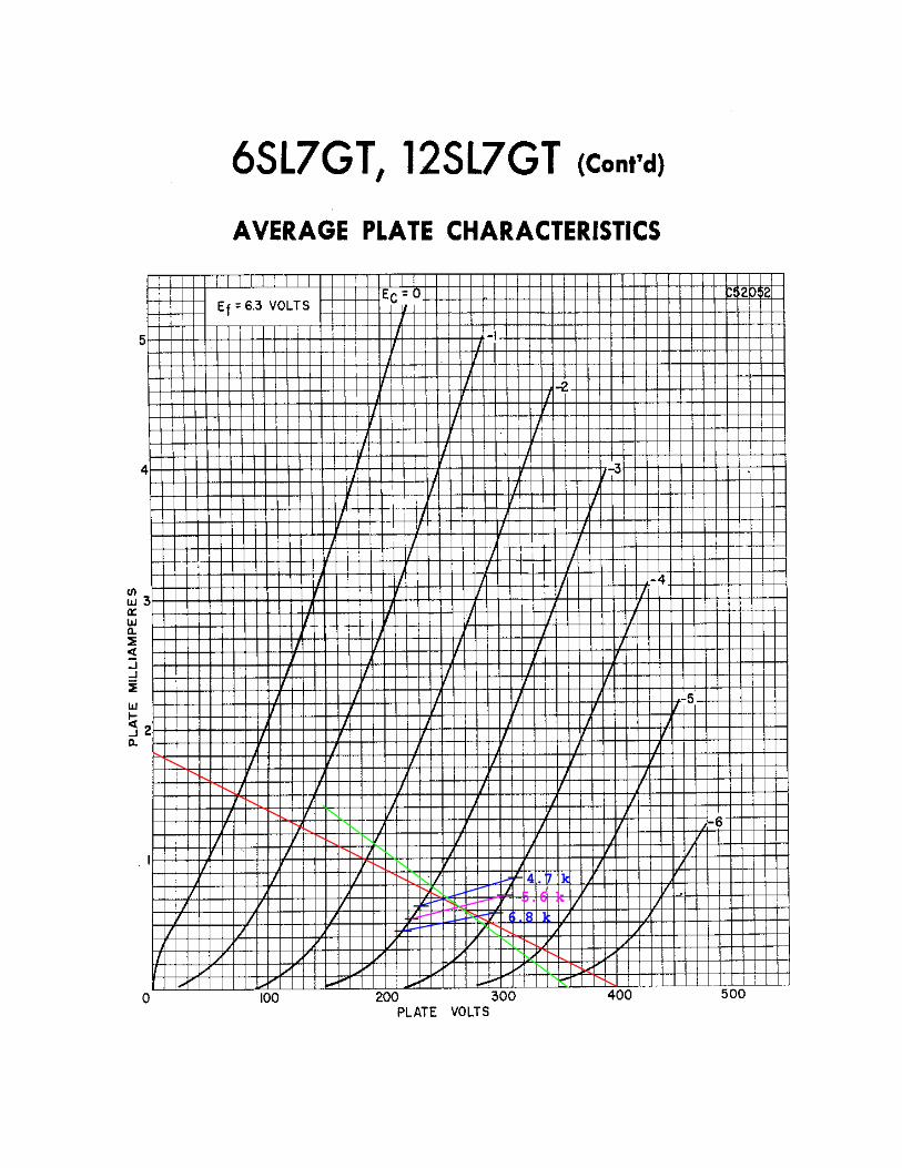
Example 6.9.
A noninverting amplifier is to have a gain of 20 dB and R2 is to be a 10 k ohm resistor. What is the necessary value of R1?
Solution:
The first step is to convert dB into gain.
A' = 10dB/20 = 1020/20 = 101 = 10.
Since A' = 1/beta to obtain a gain of 10, beta must equal 0.1. Solving equation 6.12 for R1 gives,
R1 = beta R2 / (1 - beta)
R1 = 0.1 x 10 k ohms / (1 - 0.1) = 1.11 k ohms.
6.5 The Inverting Amplifier.
Figure 6.4 Inverting Amplifier.
For a verbal description click here.
The circuit of an inverting amplifier is given in Figure 6.4. As we saw in the previous chapter the value of beta for this amplifier is given by,
beta = R1 / R2 (6.13) The approximation for the closed-loop gain is given by equation 6.7. If the gain error is large, equation 6.4 should be used to calculate the exact gain. The gain error is given by equation 6.9. The input impedance is given by,
RIN = R1 (6.14) The output impedance is given by equation 6.11.
This circuit also works because the op amp will always adjust its output until both inputs have the same potential. If a voltage of a given sign and magnitude is placed between the input terminals in Figure 6.4 the inverting input of the op amp will be placed at a potential which is determined by R1 and R2. The op amp will adjust its output until the inverting input is at the same potential as the noninverting input. Because the noninverting input is grounded, the inverting input will always be adjusted to zero potential. Figure 6.5 shows an equivalent circuit to the inverting amplifier.
Figure 6.5 Equivalent Circuit of an Inverting Amplifier.
For a verbal description click here.
Imagine that you are watching the voltmeter and adjusting the voltage of the power supply. If the polarities are as shown, you will be able to find a voltage at which the voltmeter reads zero. At this point the voltmeter current will be zero and the current in R1 equals the current in R2. If the battery is VIN and the power supply is VO then
VIN / R1 = VO / R2. (6.15) Therefore, we can write,
VO / VIN = R2 / R1. (6.16) In order to bring the voltage across the voltmeter to zero, VIN and VO must have opposite signs. The op amp does exactly the same thing. The voltmeter is replaced by the input and the power supply is replaced by the output of the op amp. The op amp will adjust its output until the voltage between the two inputs is zero. When this has been accomplished, equations 6.15 and 6.16 will be satisfied.
Example 6.10.
An inverting amplifier has the following values: R1 = 4.7 k ohms and R2 = 2.7 k ohms. The open-loop gain is 200,000. What is the closed-loop gain?
Solution:
When the open-loop gain is very high the closed-loop gain is 1/beta. Therefore, the closed-loop gain is given by,
A' = R2 / R1 = 2.7 k ohms / 4.7 k ohms = -0.574.
That's right. It's possible for an inverting amplifier to have a gain of less than unity.
Example 6.11.
An inverting amplifier is to have a gain of 30 dB and R2 is to be a 10 k ohm resistor. What is the necessary value of R1?
Solution:
The first step is to convert dB into gain.
A' = 10dB/20 = 1030/20 = 103/2 = 31.62.
Since A' = 1/beta, to obtain a gain of -31.62, beta must equal 0.03163. Solving equation 6.13 for R1 gives,
R1 = beta R2 = 0.03163 x 10 k ohms = 316 ohms.
6.6 The Summing Amplifier.
Figure 6.6 Summing Amplifier with Three Inputs.
For a verbal description click here.
The circuit of a summing amplifier is given in Figure 6.6. Remember that the op amp will adjust its output so that the voltage at the inverting input will be zero. Thus the current flowing in R2 must be the sum of the individual currents in R1A, R1B and R1C. The output voltage is given by,
VO = R2 [VINA / R1A + VINB / R1B + VINC / R1C] (6.17) A very good way to solve problems involving circuits of this kind is to treat them as circuit analysis problems.
Example 6.12.
In a circuit similar to that of Figure 6.6 the values are as follows: R1A = 10 k ohms, R1B = 7.5 k ohms, R1C = 5 k ohms, R2 = 10 k ohms, VINA = +15 v, VINB = -9 v, and VINC = -8 v. What is the output voltage of the amplifier?
Solution:
We will sum the currents at the node where the 4 resistors are joined. This node is at zero potential.
IA + IB + IC = I2.
Let us define current into the node as positive.
IA = VINA / R1A = 15 v / 10 k ohms = 1.5 mA.
IB = -9 v / 7.5 k ohms = -1.2 mA.
IC = -8 v / 5 k ohms = -1.6 mA.
I2 = 1.5 mA -1.2 mA -1.6 mA = -1.3 mA.
The net current flows out of the node; therefore, I2 must flow into the node to prevent a charge imbalance in the conductors. The current in R2 is flowing to the left, which means that the right end is positive with respect to the summing node. The voltage across R2 is I2 R2 = 1.3 mA 10 k ohms = +13 volts. Equation 6.17 will give the same answer.
The point where all of the resistors connect, (the inverting input), is often called the summing node or the summing junction. As has been said many times, this point is at zero potential. Of course it is not truly at zero potential because the amplifier does not have infinite gain. In most cases the gain of the amplifier is so high that the summing node is virtually at ground potential. The summing node is said to be a virtual ground point. It behaves as if it were actually shorted to ground.
Example 6.12 illustrates that a summing amplifier gives the negative of the true sum of the input voltages. This was one of the original uses of an operational amplifier.
Although we are not sound engineers, most of us own stereo systems and examples from that field are easy to relate to and understand. Suppose it is desired to add together the left and right channels of a stereo signal to form a monaural signal for a monaural amplifier. At the same time it is necessary to maintain the individual integrity of the left and right signals to feed a stereo amplifier. A circuit similar to Figure 6.6 but with two equal value resistors in the inputs will do the job nicely. The output will be a true L + R sum which is required for a monaural image. Because the summing node is a virtual ground, the individual L and R signals will not get mixed up in the lines before the summing amplifier. Audio engineers call this circuit a mixer but radio engineers mean something completely different when they say "mixer". Our best course is to avoid the term all together.

6.7 The Integrating Amplifier.
Figure 6.7 Integrating Amplifier.
For a verbal description click here.
The other original use of an operational amplifier was as an integrator. An integrator is an electronic circuit which takes the time integral of any function which has been converted into a time varying voltage and applied to the input of the circuit. As you can see in Figure 6.7 the feedback resistor has been replaced by a capacitor. In a real circuit there is a switch in parallel with the capacitor to be certain that it starts out with zero initial charge.
The op amp will adjust its output to keep its two inputs at the same potential. Since the noninverting input is grounded, the inverting input will also be at ground potential. The current in R is
i = vin / R. (6.18) The voltage across a capacitor is given by
The current in the resistor and the current in the capacitor are flowing in the same direction (left to right or right to left) and the connect point (summing node) is at zero potential. The voltage at the right end of the capacitor must have the opposite sign as the
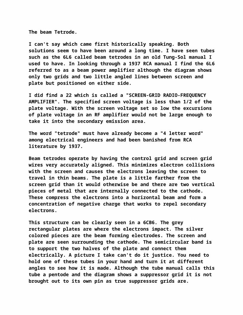
input voltage. If we substitute equation 6.18 into equation 6.19 and insert the negative sign required by the op amp we have
Now you will learn what an integral really is. Maybe you think you already know. Let's see if you do.
Example 6.13.
In Figure 6.7 the capacitor starts out with zero initial charge. The input voltage is as shown in Figure 6.8. Draw the output voltage versus time, giving scale values. R = 2 M ohms and C = 1 uf.
Solution:
The integrator's output is shown in Figure 6.9. For the first 1/2 second there is no input and the output does not change. From 0.5 to 1.5 seconds the input voltage is 1.0 volts. That is an area of 1.0. If the gain of the integrator were unity, the output would be -1 after 1.5 seconds but this one has a 2 M ohm resistor which makes the 1/RC term in front of the integral to be 1/2. The input is 1 volt for 1 second or 1 volt second. The output will change by -0.5 volts/second for 1 second to give a value of -0.5 volt. From 1.5 seconds to 2.0 seconds the input is zero and the output will not change. Notice that the output is not zero when the input is zero. When the input is zero there is no additional area being added to the integral and so the output simply stays where it is. The input is -0.5 volts from 2 to 3.5 seconds which is an enclosed area of 0.75. Because of the gain of the integrator the output will change by +0.375 volts during the 1.5 seconds when the input is -0.5 volts. The output voltage will change at a rate of 0.25 volts/second for 1.5 seconds. At the end of 3.5 seconds the output will be -0.125 volts. The output will remain at this level from 3.5 to 4.0 seconds when the input is zero. When the input goes to -1.5 volts the output will change at a rate of 0.75 volts/second for a time of 0.5 seconds. The enclosed area is 0.75 and so the output will change by an amount of 0.375 volts. The output will end up at a voltage of +0.25 volts. The output will remain at this level until there is additional input or the capacitor is discharged. There is no requirement that the output come back to zero.
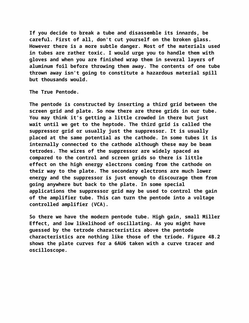
Figure 6.8 Integrator Input Voltage Versus Time.
For a verbal description click here.
Figure 6.9 Output Voltage of an Integrator.
For a verbal description click here.
Integrating amplifiers were used in analog computers to solve differential equations. They still can be used for that but digital computers will do it with more accuracy.
6.8 Single Power Supply Operation.
The major advantage of operating op amps from two power supplies is that the input to and output from the op amp can be positive or negative. Because the input voltage can be zero, slowly changing DC voltages may be amplified, added or integrated.
In some applications it may not be necessary to have a bipolar output or the signals to be processed may be AC only. In such a case it is best to power an op amp from a single power supply. One power supply is less costly, smaller, lighter and generates less heat than two power supplies.
Figure 6.10 Single Power Supply Noninverting Amplifier.
For a verbal description click here.
Figure 6.10 is the circuit of a noninverting amplifier with a gain of 10 which operates from a single power supply. The parts which distinguish this circuit from a dual power supply amplifier are the two 180 k ohm resistors in the noninverting input circuit and the capacitors in the input, output and feedback portions of the circuit. The purpose of the 180 k ohm resistors is to bias the noninverting input at 1/2 of the power supply voltage. The values given are typical for an op amp with BJT inputs. The only DC path to the inverting input is through R2 from the output of the op amp. For best temperature stability the parallel combination of the biasing resistors should equal R2. This makes the DC Thevenin resistance in both inputs the same. If an FET input op amp were used the resistors could be
as high as 10 M ohms each. The only requirement is that they be equal. The capacitor in the input prevents the circuit which is connected to the input from disturbing the bias on the noninverting input. Because the op amp always makes its two inputs have the same potential, the inverting input will also be at 1/2 the power supply and so the capacitor which is in series with the 10 k ohm resistor in the feedback network prevents this voltage from being disturbed. This capacitor has the additional effect of reducing the gain to unity for DC.
Figure 6.11 Single Power Supply Inverting Amplifier.
For a verbal description click here.
Figure 6.11 shows an inverting amplifier which will operate from a single power supply. This amplifier has a gain of -10. Once again the noninverting input is biased by a pair of equal value resistors to set its voltage at 1/2 of the power supply. Once again the parallel combination of the two biasing resistors should equil R2. The capacitor at the input is necessary to prevent upsetting the voltage at the inverting input.
There are some special purpose op amps which are designed for single supply operation. Their inputs may be placed at or even a little below ground even though the op amp is operating on a single positive power supply. However, the output of such an op amp can only have potentials of ground + 1.2 volts to VCC -1.2 volts. For best operation an offset should be added to the input to place the output at 1/2 of VCC.
6.9 Understanding Op Amp Specifications.
To the uninitiated an op amp specification sheet can be a bit bewildering. The table of specifications has columns for minimum, typical and maximum values. Few entries in the
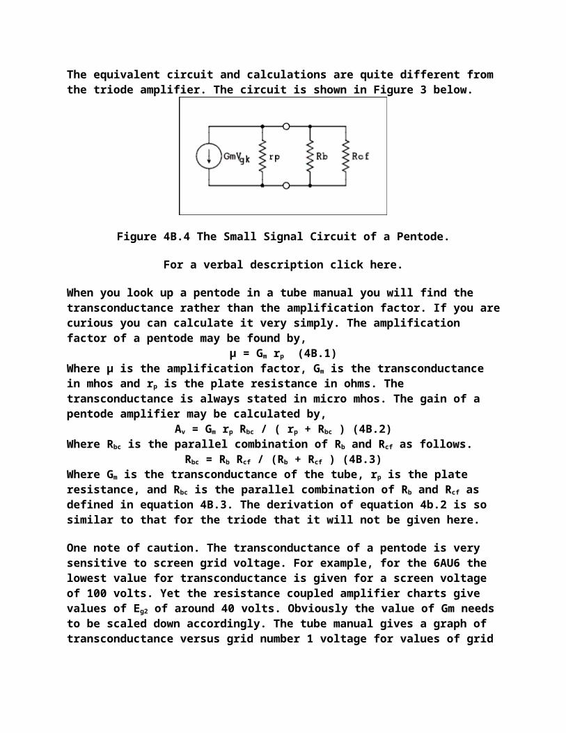
table have values under all three columns. Also there are numerous footnotes giving the conditions under which the parameter was measured. Such things as power supply voltage, load resistance, source resistance and ambient temperature can all affect the value of any given parameter.
Input Offset Voltage is the voltage which must be applied to the input terminals to bring the output exactly to zero. The typical and maximum values are given here. The untrimmed value is given, which means that no trimmer pot was connected to the pins provided for that purpose. The units are usually mV (the units are always stated in the table).
Input Bias Current is the current which flows into each input of an op amp. If the input stage is a pair of BJTs, the base current of the transistors is the bias current. If the input is a pair of FETs, the bias current is the leakage current of the P-N junction which makes up the gates of the FETs. The units may be uA, nA or pA depending on the op amp. This specification is only significant when the resistance in series with the inputs is large. If the source resistance is such that the voltage drop due to the input offset current is significant compared to the input offset voltage, the resistance in the two inputs must be equal.
Input Offset Current is the difference between the bias currents in the two inputs. If the input bias current is producing a significant drop across the source resistances, the offset current will be converted to an offset voltage by the IR drop across the source resistances.
Input Resistance is the resistance the op amp inputs present to an input signal without any feedback applied to the amp.
Input Capacitance is the effective capacitance from each input to ground including Miller capacitance.
Offset Voltage Adjustment Range is only given on op amps which have pins for an offset voltage trimmer. It indicates how large the offset can be and still be adjusted to zero.
Input Voltage Range tells how far the inputs may be moved around in potential. This is usually the voltage which the amplifier will tolerate without damage. The input voltage range for proper operation of the amplifier may be given separately as a common mode voltage rating. It is usually 2 or 3 volts less than the maximum input voltage.
Common Mode Rejection Ratio (CMRR) is the ratio of normal mode gain to common mode gain. CMRR is most often given in dB. It is defined in detail on pages 244 and 245 of this text.
Supply Voltage Rejection Ratio states how much the power supply voltage will affect the output voltage of the op amp. It is the change in power supply voltage in uV divided by the change in output voltage in volts. This parameter is measured under open-loop conditions.
Large Signal Voltage Gain is the open-loop gain.
Output Voltage Swing states over what range the output voltage can vary.
Output Resistance is the Thevenin resistance of the amplifier.
Output Short Circuit Current states how much current will flow if the output of the amplifier is shorted to ground. Most op amps have built-in current limiting to protect them from damage if a short occurs.
Supply Current is how much current the op amp will draw from the power supply.
Power Consumption is the supply current multiplied by the total power supply voltage.
Transient Response (Unity Gain) states the risetime and overshoot for a unity-gain amplifier with a step input voltage.
Slew Rate is very important because it does more to limit the upper frequency limit than does the unity gain bandwidth. It states how fast the output voltage can change and is usually given in V/us.
The Gain Bandwidth Product or Unity Gain Frequency may be given in a graph rather than in the data table. It is the frequency at which the gain is unity.
Op amp data usually contains a large number of graphs. The majority of these graphs show how various parameters are effected by temperature. If you are going to use an op amp under conditions of extreme temperature, you should not ignore these graphs. If you are looking for a particular specification and it is not in the table, it may be in the graphs.
6.10 Problems.
1. A differential amplifier has a gain of 2.00, its noninverting input is at a potential of -1 volt and its inverting input is at a potential of +2 volts. What is its output voltage?
2. A differential amplifier has a gain of 2.00, its noninverting input is at a potential of -5 volt and its inverting input is at a potential of -7.5 volts. What is its output voltage?
3. A differential amplifier has a gain of 2.00, its noninverting input is at a potential of +7.5 volt and its inverting input is at a potential of +5 volts. What is its output voltage?
4. When the normal mode voltage is changed by 30 uv the output changes by 4.5 volts. When the common mode voltage is changed by 1 volt the output voltage changes by 4.7434 volts. (a) What is the CMRR? (b) Express the CMRR in dB.
5. An op amp with a DC gain of 200,000 and gain-bandwidth product of 1 MHz is being used in a unity-gain buffer. What will be the gain error at a frequency of 200 kHz?
6. An op amp with a gain-bandwidth product of 1 MHz is being used in a unity-gain buffer. The input impedance is 500 k ohms. Over what range of frequencies will the buffer have an input resistance in excess of 10 M ohms? The DC gain is 200,000.
7. A noninverting amplifier similar to Figure 6.3 has the following values: R1 = 1 k ohm and R2 = 13 k ohms. What is the DC gain of this amplifier?
8. A noninverting amplifier is to have a gain of 12.00 and R1 is to be a 2.0 k ohm resistor. What is the value of R2 which will give the desired gain?
9. A noninverting amplifier is to have a gain of 5 dB. The series combination of R1 and R2 must be greater than 2 k ohms but the parallel combination must not exceed 10 k ohms. Select standard 5% resistor values to come as close as you can to a gain of 5 dB and remain within the requirements stated. State the resistors you selected and the actual gain in dB which these values will produce.
10. An inverting amplifier similar to Figure 6.4 has the following values: R1 = 1 k ohm and R2 = 13 k ohms. What is the DC gain of this amplifier?
11. An inverting amplifier is to have a gain of 12.00 and R1 is to be a 10 k ohm resistor. What is the value of R2 which will give the desired gain?
12. An inverting amplifier is to have a gain of 15 dB. The value of R2 must be greater than 2 k ohms but the parallel combination of R1 and R2 must not exceed 10 k ohms. Select standard 5% resistor values to come as close as you can to a gain of 15 dB and remain within the requirements stated. State the resistors you selected and the actual gain in dB which these values will produce.
13. In a summing amplifier R1A = R1B = R1C = R2. Input A is 2 volts, input B is 3 volts and input C is -1 volt. What is the output voltage of the summing amplifier?
14. In an integrator the resistor is a 1 M ohm and the capacitor is a 0.5 uf. The input to the integrator is as shown in Figure 6.12. Draw the graph of the output voltage versus time.
Figure 6.12 Input Voltage for Problem 14.
For a verbal description click here.
15. An op amp has an input offset voltage of 1.5 mV, an input bias current of 0.2 uA and an input offset current of 0.03 uA, all typical values. Assuming equal resistances in series with each input, what is the maximum resistance for the voltage due to the input offset current to equal the input offset voltage?
16. The input bias current is probably the most temperature sensitive of all op amp parameters. In an inverting amplifier the value of R1 is 47 k ohms and R2 is 120 k ohms. What resistor should be placed in series with the noninverting input to minimize the effects of temperature on the operating point?
6.11 Answers to Problems.
1. -6 Volts. 2. +5 Volts. 3. +5 Volts. 4. (a) 31,623, (b) 90 dB. 5. -0.497 % 6. 526 kHz. 7. 14.00 8. 22 k ohms. 9. R1 = 3.9 k ohms, R2 = 3.0 k ohms, Gain = 4.956 dB. 10. 13. 11. 12 k ohms. 12. R1 = 1.1 k ohms, R2 = 6.2 k ohms, Gain = 15.020 dB. 13. -4.0 volts. 14. Hint, the gain of the integrator is 2.
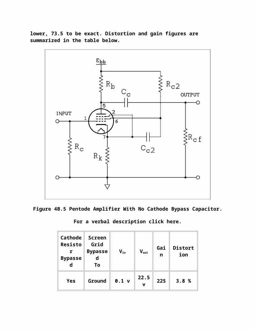
Figure 6.13 Output Voltage for Problem 14.
For a verbal description click here.
15. 50 k ohms. 16. 35.8 k ohm, nearest standard 5% value is 36 k ohm.
This page copyright © Max Robinson. All rights reserved.
Chapter 7 &EMSP; Operational Amplifier Circuits.
Instrumentation 7.1 Amplifier. AC Voltmeter 7.2 Circuit. Open-loop 7.3 Linearization. Absolute Value 7.4 Amplifier. Log 7.5 Converter. Active 7.6 Filters. Problems. 7.7 Answers to 7.8 Problems.
Chapter 7Operational Amplifier Circuits.
The best thing about op amp circuits is that it is hard to keep them from working. Although none of the circuits in Chapter 6 was indicated as having been laboratory tested, you can build any of them and they will work! Because of this increased reliability over discrete transistors, anyone who works with electronic circuits prefers to use op amps whenever possible. Unfortunately today's low cost op amps will not perform much above the audio frequency band. If the frequency range permits, op amps are to be preferred over discrete transistors.
7.1 Instrumentation Amplifier.
In laboratory instrumentation it is often necessary to place a sensor at some distance from the instrument to which it is connected. In such a case the long wires which connect the sensor to the instrument will act as antennas and pick up noise, (noise is any electrical signal which is in a place where it is not wanted). Using shielded cables will help but there may still be some noise pickup, especially if the voltage of the sensor is very small, requiring that the input amplifier of the instrument have a very high gain.
Figure 7.1 Signal and Noise Pickup on Long Lines.
For a verbal description click here.
The noise which is picked up on the wiring is usually common mode while the sensor is connected between the two wires so that its signal is normal mode. The situation is illustrated in Figure 7.1. Twisting the wires together to insure that they are in the same physical location will insure that the noise picked up on both wires will be the same. If the two wires are connected to the two inputs of a differential amplifier, the common mode noise on the wires will be cancelled out while the signal will be amplified. For this method of noise canceling to work properly the two inputs must have identical input impedances and gains which are equal in magnitude and opposite in sign. In addition to these requirements the gain is usually very high. An amplifier which meets all of these requirements is called an instrumentation amplifier and a circuit is shown in Figure 7.2.
Figure 7.2 Instrumentation Amplifier.
For a verbal description click here.
The best way to approach a problem involving this circuit is to treat it as a circuit analysis problem. For example, we will calculate the gain of the first amplifier stage of the circuit of Figure 7.2. The first stage consists of OA1 and OA2. If a voltage is applied between the two inputs (normal mode) the two op amps will adjust their output voltages to bring each of the inverting inputs to the same potential as the corresponding noninverting input. If we apply a voltage of VIN between the two input terminals, the identical voltage will appear across R1. This will cause a current of,
I = VIN / R1 (7.1) to flow in the series combination of the two identical resistors labeled R2 and R1. There is no significant drop across the two resistors labeled RS. The output voltage of the first stage is the total voltage drop across the resistor chain.
VO = I (R1 + 2 R2 ). (7.2) Substituting equation 7.1 into equation 7.2 and dividing through by VIN gives,
VO / VIN = (R1 + R2) / R1 (7.3) The gain of the second stage which consists of OA3 could be derived in the same way if desired. Rather than to have yet another equation to remember it is better to analyze the circuit using Ohm's and Kirchhoff's laws.
Example 7.1.
In the circuit of Figure 7.2 R1 = 2 k ohms, R2 = 99 k ohms, R3 = 10 k ohms and R4 = 100 k ohms. If the voltage at the top input is +2.0 mV and the voltage at the bottom input is -1.0 mV, what is the output voltage?
Solution:
The best way to keep track of voltages is to make a chart of all three terminals of all three op amps as shown. The voltages at the noninverting inputs of OA1
Terminal OA1 OA2 OA3
noninverting input +2 mV -1 mV 136.81818 mV
inverting input +2 mV -1 mV 136.81818 mV
Output 150.5 mV -149.5 mV 3.00 V
and OA2 are given and so can be filled in immediately. The op amps will make the voltage at the inverting input be the same as that at the noninverting input and so these values can also be filled in by inspection. The voltage across R1 is 2 mV -(-1 mV) = 3 mV. The current in R1 is I = 3 mV / 2 k ohms = 3/2 uA. The voltage drop across either R2 is V = 3/2 uA x 99 k ohms = 148.5 mV with the upper end positive. The lower end of the top R2 is at a potential of +2 mV; therefore, the upper end of the top R2 is at 2 mV + 148.5 mV = 150.5 mV. The
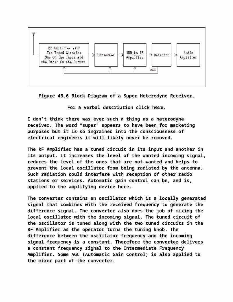
upper end of the bottom R2 is at -1 mV; therefore, the lower end is at (-1 mV) + (-148.5 mV) = -149.5 mV. Notice that the difference is 150.5 mV - (-149.5 mV) = 300 mV. This confirms a first-stage gain of 100. The voltage at the noninverting input of OA3 is found by simply applying the voltage divider equation to R3 and R4. The noninverting input of OA3 does not load the voltage divider. V+3 = VO1 R4 / (R3 + R4) = 150.5 mV x 100 k ohms / 110 k ohms = 136.81818 mV. The entries for both the noninverting input and the inverting input of OA3 can now be filled in. The voltage drop across the bottom R3 is 136.81818 mV - (-149.5 mV) = 286.31818 mV. The current through the lower R3 is I = 286.31818 mV / 10 k ohms = 28.631818 uA. The voltage drop across the lower R4 is 28.631818 uA x 100 k ohms = 2863.1818 mV with the right end positive. The voltage at the output of OA3 is its inverting input voltage + the drop across the lower R4, which is 136.81818 mV + 2863.1818 mV = 2999.99998 mV which, when rounded off, gives 3.00 volts.
The results of this example confirm that the gain of the second (OA3) stage is given by
A' = R4 / R3 (7.4) even though the circuit appears more complicated than an ordinary inverting amplifier.
The input to the circuit of Figure 7.2 is a differential input because neither side of the input needs to be connected to ground. The output of the first stage (OA1 and OA2) is a differential output because neither side is connected to ground. The input to the second (OA3) stage is also differential. The output from OA3 is said to be single-ended because one side is connected to ground. Thus a circuit consisting of two R3s, two R4s and an op amp can be used to convert a differential source to a single-ended load. The problem with using such a circuit is that the input resistances at its two inputs are not equal. The input resistance at the noninverting input is R3 + R4 while the input impedance at the inverting input is R3. The two noninverting amplifiers serve to balance the input impedances and at the same time make them very high.
Connecting R1 between the two amplifiers instead of each amplifier having its own R1 makes the amplifiers self-balancing, which increases the common mode rejection ratio. Note in the example that even though the original inputs had a 2 to 1 imbalance, the outputs had less than a 1% imbalance. The OA3 stage can easily accommodate the small imbalance. If this circuit is to have a high CMRR the values of the two R3s and the two R4s must be very well matched.
The resistors RS are used to prevent serious imbalance due to input bias currents in the event that the source has a high Thevenin resistance. If input bias current is no problem the two resistors may be omitted (replaced by pieces of wire).
7.2 AC Voltmeter Circuit.
Voltmeters, whether analog or digital, are basically DC measuring instruments. When it is desired to measure AC the common practice is to change the AC to DC and then measure it. This causes problems because the diodes which are used to rectify the AC are not linear. Perhaps the oldest approach is to print a separate scale on the face of the meter, (analog
meters), and instruct the operator to read that scale when measuring AC. This method has worked well for many decades in meters which have no electronic circuits inside them.
Electronic voltmeters use some electronic tricks to make the response of the rectifiers linear. The circuit of a linear AC voltmeter is shown in Figure 7.3.
Figure 7.3 Linear AC Voltmeter Circuit.
For a verbal description click here.
If you trace the current through the bridge as was done in Chapter 3 the current will be seen to be flowing in or out of the op amp output, through one of the top diodes in the bridge, through the meter from right to left, through one of the bottom diodes and up or down through the resistor R2 to ground. The feedback is taken from the top of the resistor which makes the voltage waveform across R2 match the input waveform. Because R2 is a resistor, its current waveform will match the input voltage waveform. The meter and the resistor are in series. The same current is flowing in the meter as flows in R2. The meter current is the absolute value of the R2 waveform but the magnitudes are identical. If you look at the output voltage waveform on a scope, you will see a very distorted wave. What you are seeing is what has been said many times, "The op amp will adjust its output voltage to make the inverting input voltage equal the noninverting input voltage." The output voltage will be whatever it has to be to make the current in R2 directly proportional to the input voltage. In this case it is the meter current which is being linearized. Since the pointer responds to the meter current, the deflection of the pointer will be linearly proportional to the average input voltage. The meter can be calibrated to indicate the RMS of a sine wave.
The value of R2 sets the full-scale range of the meter. With the value given the range will be approximately 1 volt if a 1 mA meter is used. The 100 pf capacitor is to prevent the op amp from oscillation at high frequencies. This capacitor will cause the meter to lose accuracy at high frequencies and if you want to measure voltages of high frequency waves the capacitor
must be as small as possible while still preventing oscillation. The capacitor at the input is necessary to block any DC which may be mixed with the AC to be measured.
7.3 Open-loop Linearization.
Occasionally in a physics lab it is necessary to make a measurement on some sensor which is at a very high potential. When this is the case a way must be found to transfer the electrical signal and still not have any direct electrical connection. That may seem impossible but don't forget about the transformer which transfers electrical energy while providing electrical isolation. If the sensor delivered AC, a transformer could be used to couple the signal while isolating it. Unfortunately most sensors deliver a slowly changing DC. One approach often used is to change the DC to a proportional AC and then pass it through a transformer for isolation. After isolation the signal may be processed in any manner desired.
Figure 7.4 Open-loop Linearized Photocell.
For a verbal description click here.
A somewhat simpler method of isolation is shown in Figure 7.4. The input signal (from the sensor) is applied to the inverting input of the op amp. The feedback is taken to the noninverting input of the amp. That may seem to be positive feedback but the lamp and photocell have something to say about that. As the voltage at the output of the op amp goes positive, the lamp grows brighter. As the photocell receives more intense illumination its resistance decreases. As the resistance of the photocell decreases the voltage at the noninverting input of the op amp will be decreased. The combination of the lamp and photocell provide the inversion and so the op amp does not have to.
When a positive voltage is applied to the input the op amp will adjust the brightness of the lamp so that the voltage across the photocell on the left is equal to the input voltage. If the
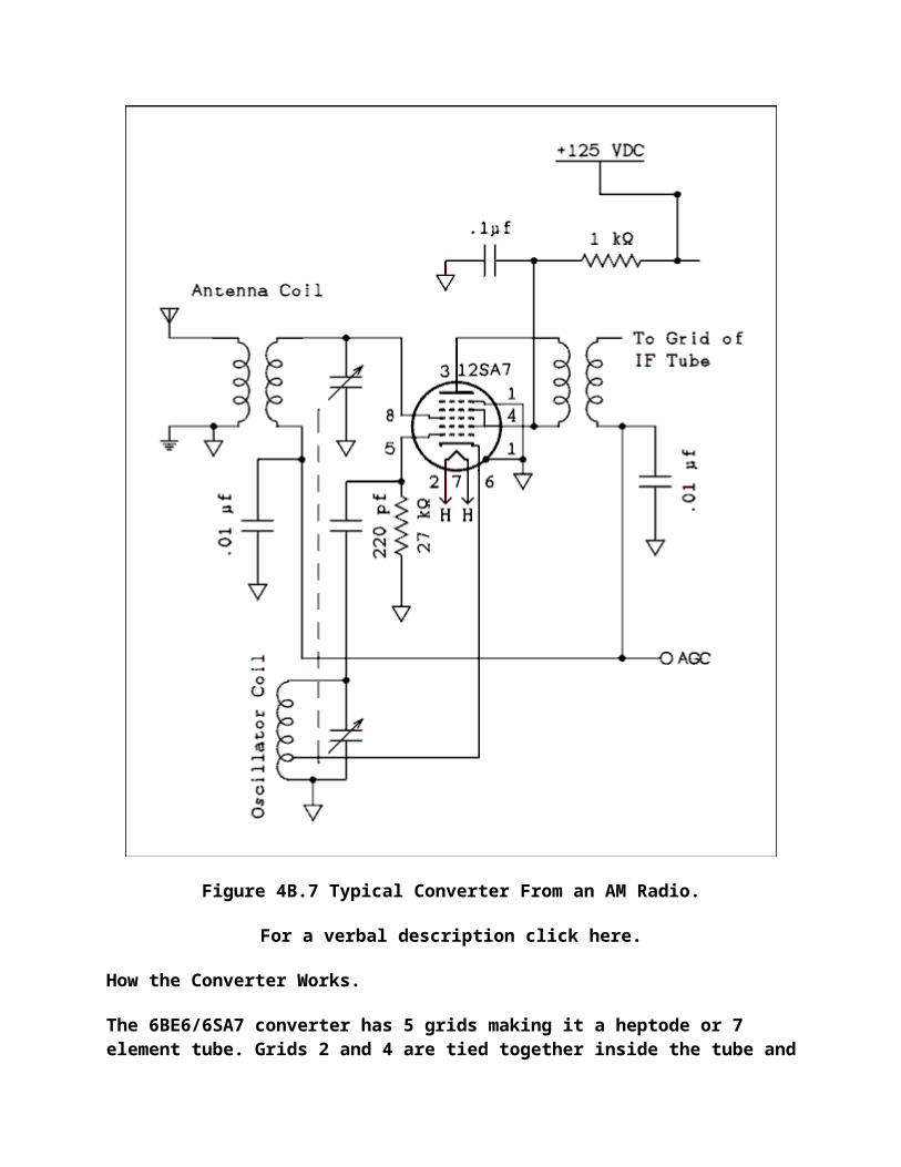
two photocells are closely matched the voltage across the photocell on the right will also be equal to the input voltage. Because there is no electrical connection between the two parts of the circuit, the input can be at any arbitrarily high potential and allow the output to be grounded.
In this circuit the batteries are meant to be batteries. The circuit should be constructed in an insulated box to prevent accidental electric shock. The value of the resistor and pot which are in series with the photocells depend on the illuminated resistance of the photocells. The values of these resistors will have to be determined after the photocells are obtained. The purpose of the two diodes in series with the lamp is to permit the lamp voltage to go all the way to zero. The output of an op amp will have a minimum voltage of 2 P-N junctions from the negative power supply lead. The circuit only works for positive input voltages. If a negative input is applied, the lamp will attempt to get darker than dark and nothing will happen, except in the twilight zone.
7.4 Absolute Value Amplifier.
The AC voltmeter circuit given above will change AC to a linear meter reading but sometimes it is necessary to change an AC to a linearly proportional DC voltage. Simple rectifiers of the type used in power supplies are not linear and indeed have no output for the first 0.6 volts of the input signal. If the diodes are placed in the feedback loop of an op amp (two op amps in this case) the rectified output will be directly proportional to the input. The circuit of a linear rectifier or absolute value amplifier is shown in Figure 7.5.
Figure 7.5 Absolute Value Amplifier.
For a verbal description click here.
When an AC signal applied to the input goes positive, the output of OA1 goes negative. This reverse biases D2 and forward biases D1. The output of OA1 is disconnected from the output of the circuit. Meanwhile, the output of OA2 goes positive. This forward biases D4 which connects the output of OA2 to the output of the circuit. D3 is reverse biased as we will shortly see. The inverting input of OA2 is connected to the output node through R3. The op amp will adjust its output to whatever voltage is necessary to bring the output node to the same potential as the input node. That will cause the output of OA2 to be about 0.6 volts more positive than the input node of the circuit. D3 is therefore reverse biased by 0.6 volts. For a positive input, the output is also positive and has the same voltage.
When the input goes negative the output of OA2 goes negative, which reverse biases D4, disconnecting the output of OA2 from the output node of the circuit. D3 is forward biased. For a negative input, the output of OA1 will go positive. D2 is forward biased and D1 is reverse biased. Resistor R2 takes feedback from the output node and if R1 and R2 are of equal value the output node will have the same magnitude and opposite sign as the input node. Thus for a negative input the output is positive but has the same magnitude as the input.
If a capacitor is placed in parallel with R4 the circuit becomes a peak detector. If an RC low-pass filter is connected to the output the circuit becomes an average value detector. In the latter case the resistor in the low-pass filter should be greater than 1 M ohms for an error of less than 1%. In either case the value of the capacitor will depend on the response time required.
7.5 Log Converter.
This section has been rendered obsolete by the low cost of powerful desk top computers and data collection systems. It has been left in to show how things were a few years ago.
If it is necessary to take the log of data which is being collected in an experiment, the method of choice is to digitize the data and let a computer do the log taking. In very well-funded laboratories the computer is on-line, (connected to the experimental equipment). In less well-funded experiments the data must be hand carried - on disk, tape or paper - to the computer.
It is always desirable and often necessary to see the log of the data as the experiment is running. Seeing the log of the data may be necessary in order to properly adjust the equipment. If the experimenter is able to see the data come out as the experiment runs, it is possible to tell if something has gone wrong. A strip-chart recorder is often used for this purpose.
Many experiments deliver the data in analog form and most strip-chart recorders accept data in analog form. For the purpose of so-called "quick look" data reduction an analog device which will take the log of analog data may be helpful.
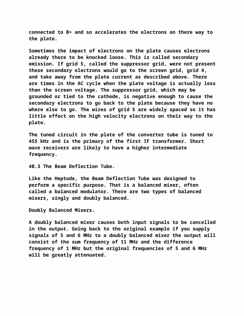
The circuit of a working logarithmic converter is shown in Figure 7.6. This circuit is designed to be used with a strip-chart recorder having a Y axis input of 10 mV full- scale. With the values given the unit may be calibrated to 1 mV = 10 dB. The converter operates from two 9 volt transistor radio batteries.
Figure 7.6 Logarithmic Converter for Use witha 10 mV Strip-chart Recorder.
For a verbal description click here.
The op amp is a type 558 which has two amplifiers in a single 8 pin package. The transistors used here were from the junk box. Any low power PNP transistors will do so long as they are reasonably well matched.
The batteries are connected as shown in Figure 6.1. A double pole switch is required to interrupt the current from both batteries.
The input signal is applied through R1 to the inverting input of OA1 which is nothing more than a unity-gain inverter. R5 is a zero adjust control. The op amp used has no offset adjustment pin connections and so the somewhat elaborate network of R4 through R9 is required to provide offset adjustment for the op amp.
Transistor Q1 is the element which does the log taking. The I-V curve of a P-N junction is an exponential or a logarithmic function depending on how you look at it. In this circuit we are looking at it as a log function. If a positive input signal is applied to the input, it will be inverted and appear at the output of OA1 as a negative voltage. This will cause current to
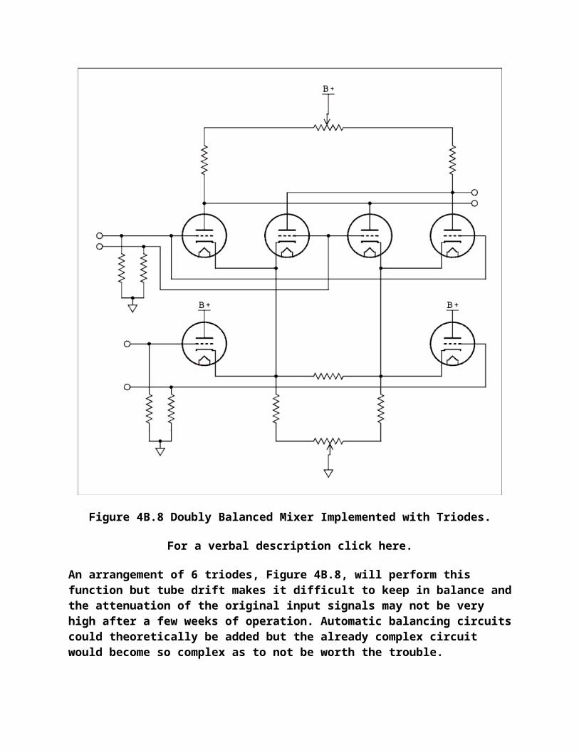
flow to the left in R10. The output of OA2 will adjust itself so that the collector current of Q1 is equal to the current in R10. The voltage at the op amp's output will be adjusted so as to forward bias the base-emitter junction of Q1. If the input voltage changes, the collector current of Q1 will change linearly and the base-emitter voltage will change logarithmically.
Transistor Q2 serves to temperature compensate the circuit. For example, if the temperature goes up, the base- emitter voltage of Q1 will decrease, which will lower the output voltage. At the same time the temperature of Q2 will increase and its base-emitter voltage will also decrease. The decreased drop across Q2 will increase the output voltage which will compensate for the decrease caused by Q1. Q1 and Q2 should be in physical contact to insure that they are at the same temperature. If the transistors are in metal packages, they should be electrically insulated from each other because the case is often connected electrically to one of the transistor elements.
The network of R12 through R14 reduces the output voltage to the proper level for the 10 mV chart recorder. R13 should be adjusted for a span of 10 dB per mV at the upper end of the working range. R5 may be used to correct errors at the low end of the range. The unit will not have a working range of 100 dB as implied by 10 / mV over a range of 10 mV. The best achievable is about 50 dB. Below -50 dB the response tends to become linear rather than logarithmic.
If the input voltage is negative, OA2 will go to full negative saturation which will slam the chart recorder's pen down hard against the zero stop. The log of a negative number is undefined in the analog world as well as in the world of numbers. The only capacitor in the circuit is to prevent OA2 from oscillating at ultrasonic frequencies.
7.6 Active Filters.
A single RC filter provides a roll off in the stop-band of 20 dB per decade. Cascading filters (connecting the output of one to the input of the next) does not work as well as might be expected. The roll off around cutoff is so gradual that the filter begins to affect the output long before any large values of attenuation are reached. A single LC filter section will give a roll off of 40 dB per decade and it affects the output only slightly on the pass-side of cutoff. Attenuation increases quickly on the stop-side of cutoff. The problem is that inductors are large, heavy, expensive and often difficult to find. The solution is an active filter. An op amp circuit which has only resistors and capacitors in addition to the op amp can simulate an LC filter. Several of such circuits could be placed in the same volume of one inductor.
Figure 7.7 shows a high-pass filter circuit. In this circuit if C = 0.01 uf and R = 10 k ohms the cutoff frequency is 2.8 kHz and the attenuation at 60 Hz is 50 dB. The cutoff frequency can be calculated from,
fC = 1 / (3.5 R C) (7.5)
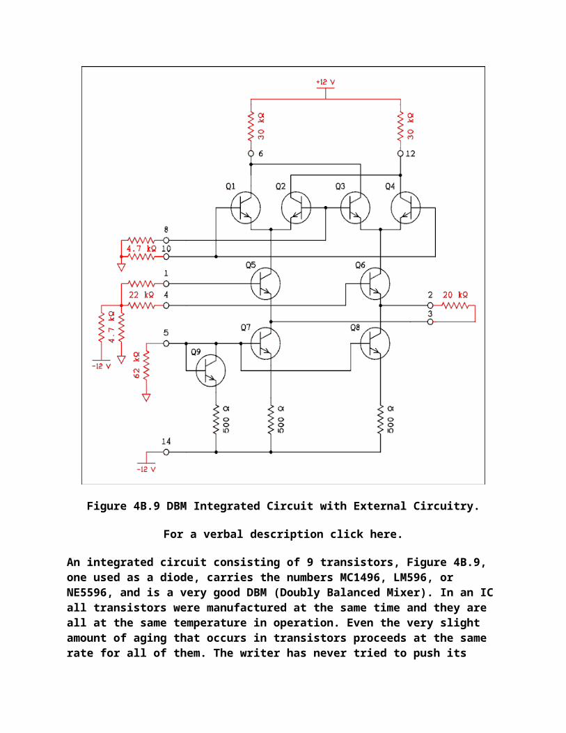
Figure 7.7 High-pass Active Filter Circuit.
For a verbal description click here.
The op amp is used as a unity-gain buffer. In order to insure good performance, the gain error should be less than the desired measurement accuracy at the highest frequency to be passed.
Figure 7.8 shows a low-pass filter circuit. In this circuit if C = 0.1 uf and R = 150 k ohms the cutoff frequency is 4.5 Hz and the attenuation at 60 Hz is 36 dB. The cutoff frequency can be calculated from,
fC = 1 / (15 R C) (7.5)
Figure 7.8 Low-pass Active Filter Circuit.
For a verbal description click here.
The op amp is used as a unity-gain buffer. In order to insure good performance, the gain error should be less than about 5% at 10 times the cutoff frequency.
Example 7.2.
It is desired to construct a low-pass filter with a cutoff frequency of 0.1 Hz. The capacitors to be used have a value of 1.0 uf. (a) What is the calculated value of R? (b) What standard values should be used for the two resistors in the filter?
Solution:
(a) Solving equation 7.6 for R gives R = 1 / (15 fC C) =1 / (15 x 0.1 x 1 x 10-6) = 667 k ohms
(b) The closest value for R is 680 k ohms and the closest value for 2R is 1.3 M ohms.
7.7 Problems.
1. In the circuit of Figure 7.2 R1 = 200 ohms, R2 = 99.9 k ohms, R3 = 10 k ohms and R4 = 1 M ohm. If the voltage at the top input is -20 uV and the voltage at the bottom input is -70 uV, (a) what are the voltages at each of the op amp terminals? Make a chart similar to that in Example 7.1. (b> What is the gain of the amplifier?
2. Using the circuits given in this chapter draw the schematic diagram of a circuit which will take an AC signal and rectify it without introducing significant errors. Then the circuit must average the rectified AC and convert it to dB.
3. Design a high-pass filter which has a cutoff frequency of 10 kHz. The capacitors have a value of 0.0033 uf. Give the standard values for the resistors to be used in the circuit. Draw the circuit.
7.8 Answers to Problems.
1. The table shows the values.
Terminal OA1 OA2 OA3
noninverting input -20 uV -70 uV 24.7079208 mV
inverting input -20 uV -70 uV 24.7079208 mV
Output 24.9550000 mV -25.0450000 mV 5.0000000 V
2. (b) 100,000
3. The averaging could be accomplished using a passive RC filter but I decided to go all out. If you drew an RC filter, your answer is correct.
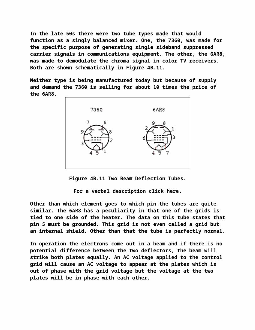
Figure 7.9 Answer to question 2.
For a verbal description click here.
4. R = 9.1 k ohms, 2R = 18 k ohms. The circuit is like figure 7.7.
This page copyright © Max Robinson. All rights reserved.
Digital Circuits. Chapter 8
The Binary Number 8.1 System. Logic Functions and 8.2 Gates. Boolean 8.3 Algebra. Combinational Logic 8.4 Circuits. Flip-Flops and 8.5 Counters. Displaying the 8.6 Count. Multiplexed 8.7 Displays. Digital to Analog 8.8 Converter. Analog to Digital 8.9 Converter.8.10 The 555 Timer.8.11 Problems.8.12 Answers to Problems
Chapter 8Digital Circuits.
Up to this point we have been dealing with analog signals. An analog signal is a voltage or current which carries information and can take on any value. For example the output of a thermocouple can be 31.56 uV or 103.97 uV or even 1.6358 mV. The point is that the only limit is our ability to measure the voltage. The voltage itself may have a value of 1.63582419574239658395723656793445642467543 mV for all we know. Analog data is quantized (if at all) only by the measurement technique. The data itself may take on any value.
Digital data on the other hand is presented as numbers. Two forms you are likely familiar with are the readout of the digital multimeter and the data stored in a computer. The values of digital data are quantized. For example if the data is only available to 3 significant digits then the data can only have values such as 3.82 and 3.83. The datum cannot take on a value between 3.82 and 3.83.
8.1 The Binary Number System.
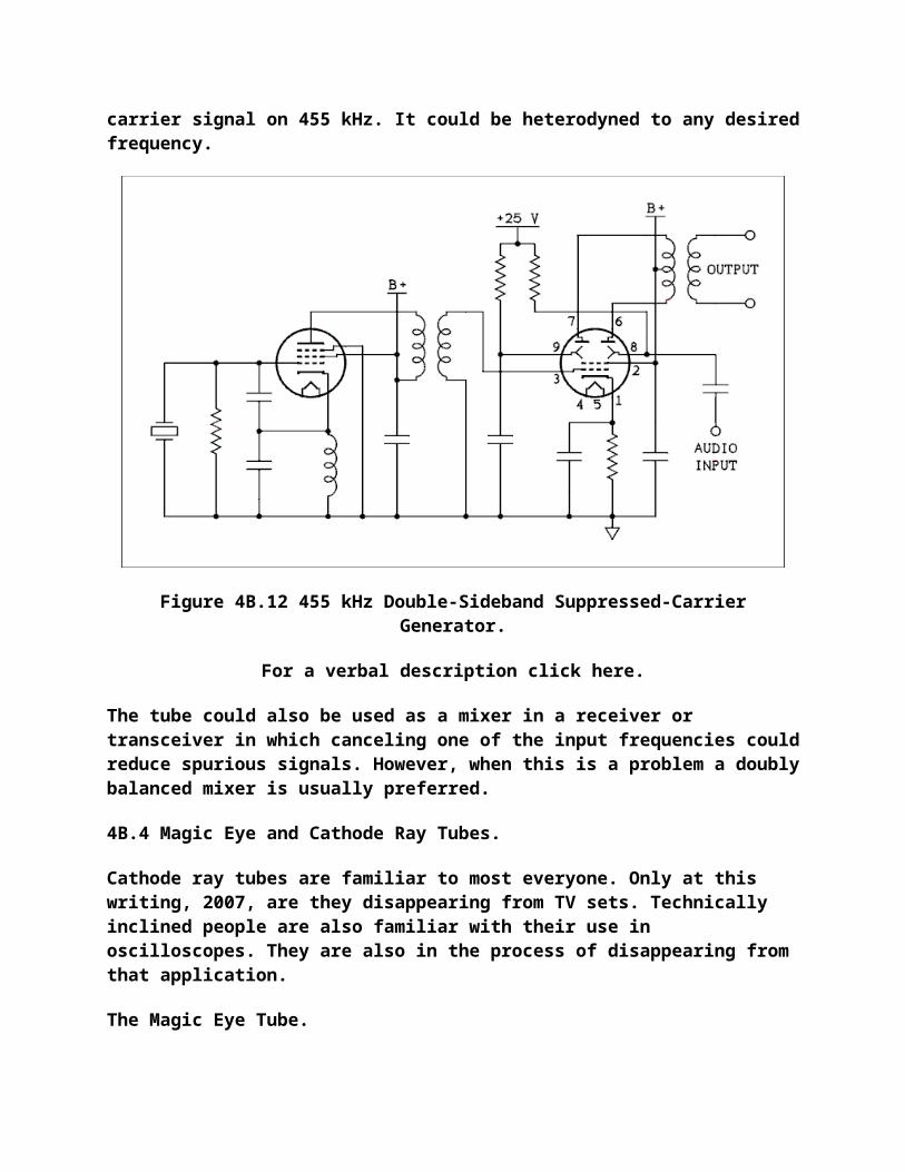
The number system we use has ten digits (0 through 9) and we write numbers by using a system of positional weighting. The earliest computer circuits attempted to emulate this system. For example there might be a set of four different voltages, each voltage could be zero, 1 volt, 2 volts, and so on to 9 volts. One of the voltages could be used to represent units, another tens, the third hundreds and the fourth thousands. While this sounds workable in theory and easy to use, in practice the circuits become very complex and expensive to construct.
The system of binary numbers has been around for more than a century but it had no practical use until the digital computer came along. Instead of using a number system where each digit can take on ten different values it is much easier to let each digit have only two values. For example, if we have a set of voltages and each can be either 0 volts or 5 volts, we can use a system of positional weighting as shown in Figure 8.1.
28 27 26 25 24 23 22 21 20
256 128 64 32 16 8 4 2 1
0 1 1 0 0 1 0 1 1
Figure 8.1 Example of a 9 Digit Binary Number. The first line in Figure 8.1 gives the power of 2 for each position in the binary number system. The second line gives the actual values of each position. The third line is an example of a binary number. The number is 203 decimal. The position values continue on to the left 29, 210, etc, for as far as is needed.
To convert a binary number to decimal all that is necessary is to add the positional values in all columns where the binary digit has the value 1. In Figure 8.1 it is 128 + 64 + 8 + 2 + 1 = 203. Figure 8.2 shows what counting in binary looks like.
0 0 0 0 0 0
1 0 0 0 0 1
2 0 0 0 1 0
3 0 0 0 1 1
4 0 0 1 0 0
5 0 0 1 0 1
6 0 0 1 1 0
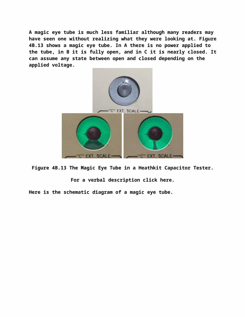
7 0 0 1 1 1
8 0 1 0 0 0
9 0 1 0 0 1
10 0 1 0 1 0
11 0 1 0 1 1
12 0 1 1 0 0
13 0 1 1 0 1
14 0 1 1 1 0
Figure 8.2 Counting in Binary Numbers.The term "binary digit" has been shortened to the word "bit". A bit is a binary digit. A number which has 8 binary digits is said to be an 8 bit number. A bit is allowed to have only two values: 0 and 1.
Binary Addition.
Addition in binary is just like addition in decimal (if you're missing eight fingers). The rules for addition are summarized in Figure 8.3.
Bits to be added 0 + 0 0 + 1 1 + 1 1 + 1 + 1
Sum 00 01 10 11
Single Bit Sum 0 1 0 1
Carry 0 0 1 1
Figure 8.3 Rules for Addition of Binary Digits.
Binary addition is limited to two binary numbers because of hardware limitations. However, if the addition of the bits to the right produced a carry the current pair of bits must include provisions for a third bit to be added. The last column allows for both bits being added to be 1 and the addition to the right to produce a carry of 1.
Example 8.1.
What is the sum of 100111 and 1011?
Solution:
As with decimal numbers the shorter number must be filled out with zeros on the left.
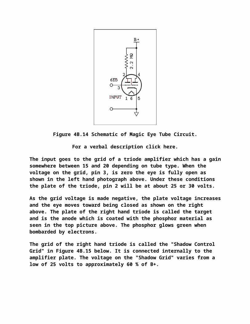
Carried 0 1 1 1 1
First number 1 0 0 1 1 1
Second number 0 0 1 0 1 1
Sum From Figure 8.3 1 1 10 10 11 10
Write Down 1 1 0 0 1 0
And Carry 0 0 1 1 1 1
We'll learn multiplication in the second grade.
8.2 Logic Functions and Gates.
We can do more with binary digits than just add them. We can perform the logic functions AND, OR and NOT on them. Since binary digits (bits) only have two states they can be used to represent anything which has two states. For example a lamp can be either on or off, a switch can be either closed or open, an answer can be either true or false; each of these may be represented by a bit which is either 1 or 0.
Suppose we connect up three switches as shown in Figure 8.4. What we know about circuits tells us that all three switches must be closed to turn on the lamp. If we set up the rule that 1 = closed = lighted we can write a table as in Figure 8.5.
Figure 8.4 AND Function Illustrated Using Switches.
For a verbal description click here.
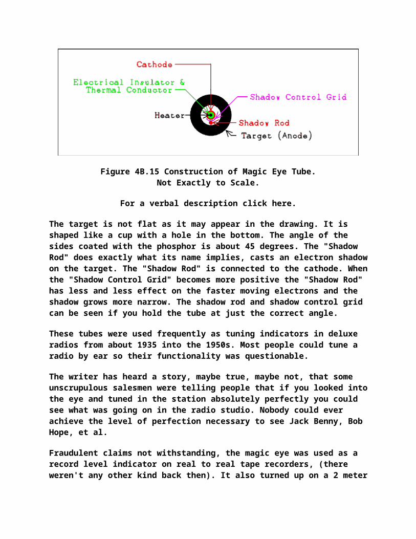
A B C LAMP
0 0 0 0
0 0 1 0
0 1 0 0
0 1 1 0
1 0 0 0
1 0 1 0
1 1 0 0
1 1 1 1
Figure 8.5 Truth Table for AND Function.
This is referred to as an AND function because to get the lamp to glow it is necessary to close switches A and B and C. A table which lists all possible combinations of inputs (stimuli) and the response for each combination is called a "truth table".
If we connect three switches in parallel, as in Figure 8.6, we have an OR function. If any one switch is closed the lamp lights. This is referred to as an OR function because to get the lamp to glow it is only necessary to close switch A or B or C. It makes no difference if more than one switch is closed, the lamp stays on. This is the inclusive OR function. It is always referred to simply as the OR function. The truth table for the OR function is shown in Figure 8.7.
Figure 8.6 OR Function Illustrated Using Switches.
For a verbal description click here.
A B C LAMP
0 0 0 0
0 0 1 1
0 1 0 1
0 1 1 1
1 0 0 1
1 0 1 1
1 1 0 1
1 1 1 1
Figure 8.7 Truth Table for OR Function.
The two remaining functions cannot be illustrated using switches and lamps. The functions are NOT and Exclusive OR, referred to as XOR.
The NOT function is simply a state inverter. If the input is 0 the output is 1. If the input is 1 the output is 0. An inverter can have only one input. The truth table for an inverter is given in Figure 8.8.
INPUT OUTPUT
0 1
³ 1 0
Figure 8.8 Truth Table for Logic Inverter
An exclusive OR (XOR) function can only have two inputs. The XOR function is similar to the OR function except that if both inputs are 1s the output is 0. The output is true (1) if A is 1 or B is 1 but the case of A = B = 1 is excluded. The truth table for an XOR function is shown in Figure 8.9.
A B LAMP
0 0 0
0 1 1
1 0 1
1 1 0
Figure 8.9 Truth Table for XOR Function.
Logic functions are implemented with transistors, diodes and resistors which are packaged in integrated circuits. For the purpose of drawing schematic diagrams each logic function has a schematic symbol. They are given in Figure 8.10. A circuit which performs a given logic function is called a logic gate.
Figure 8.10 Schematic Symbols for Logic Gates.
For a verbal description click here.
The NAND and NOR gates which are shown in the schematic symbols are combinations of the NOT and AND, and the NOT and OR functions respectively. The truth tables for the NAND and NOR gates are given in Figure 8.11.
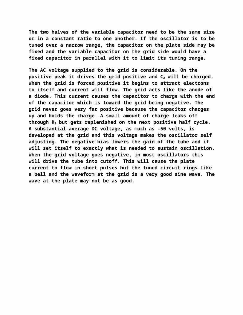
Figure 8.11 Truth Tables for NAND and NOR Gates.
It is not important to know the internal schematic diagram of a logic gate. If it were to be given here the reader would most likely not remember it. The curious reader is referred to IC data books most of which give the internal diagrams.
Logic Families.
The first digital ICs were essentially the same as the circuits of the BJT switches studied in chapter 4. These ICs employed more resistors than transistors. It is normal in discrete circuitry to use more resistors than transistors because resistors are less costly than transistors. A peculiarity of ICs is that it is actually cheaper to make transistors on a chip than it is to make resistors. Circuits were developed which would have been impractical to construct using discrete circuitry. They used more transistors than resistors.
Those first-generation ICs were called RTL for Resistor- Transistor-Logic. The logic family which contains more transistors than resistors is called TTL for Transistor- Transistor-Logic. There was an intermediate stage of development which used a large number of diodes. This family was called DTL for Diode-Transistor-Logic. Of these the only one in use today is TTL.
The two most important logic families today are TTL Transistor-Transistor-Logic and CMOS Complementary-Metal- Oxide-Semiconductor logic. Each logic family is being subdivided into many subfamilies which since this book was originally written have increased exponentially. These subfamilies are too numerous to cover in detail here. We will look briefly at a few of the most important subfamilies.
7400 Series TTL.
NAND
A B C OUTPUT
0 0 0 1
0 0 1 1
0 1 0 1
0 1 1 1
1 0 0 1
1 0 1 1
1 1 0 1
1 1 1 0
NOR
A B C OUTPUT
0 0 0 1
0 0 1 0
0 1 0 0
0 1 1 0
1 0 0 0
1 0 1 0
1 1 0 0
1 1 1 0

This family is the father of the TTL family. Because it is constructed with BJTs it has low input impedance and low output impedance. It operates from a 5 volt power supply. Each gate output can drive 10 inputs of other gates.
An input voltage in the range of 0 to 0.8 volts is recognized as a logic 0 while an input voltage in the range of 2 to 5 volts is recognized as a logic 1. If the input voltage is between 0.8 and 2 volts there is no guarantee as to what will happen.
74LS00 Series Low-power Schottky TTL.
This subfamily operates at about 1/10 the power and about twice the speed of standard TTL. Because of the speed and power difference it is not advisable to mix 74-- and 74LS-- ICs in the same circuit (unless you are sure of what you are doing).
74C00 CMOS.
The ICs in this subfamily are pin compatible with the corresponding 74-- or 74LS-- of the TTL families. However, they are NOT electrically compatible. Like all CMOS they operate from a power supply anywhere in the range of 3.6 to 15 volts. They have very high input impedance and medium output impedance. Because the logic levels are incompatible CMOS and TTL cannot be mixed even if operated from the same power supply.
In CMOS an input voltage in the range of 0 to 1/3 VCC is recognized as a logic 0 while an input voltage in the range of 2/3 VCC to VCC is recognized as a logic 1. If the input voltage is between 1/3 VCC and 2/3 VCC there is no guarantee as to what will happen.
74HC00 Series.
This is a hybrid of TTL and CMOS. It operates at TTL speeds but is level compatable with CMOS. It operates from 5 volts.
4000 Series CMOS.
The 4000 series CMOS has the same logic levels as the 74C00 CMOS. The series contains a wide variety of gates, flip-flops, counters and other special purpose ICs not found in the 74C00 series.
CMOS has a reputation of being subject to burnout from handling. Like the black widow spider and the tarantula, its reputation is undeserved. The input pins are protected by diodes which make the ICs quite rugged. Normal prudence is all that is required when handling these ICs. The writer has completed several projects using CMOS ICs and has yet to burn one out due to handling.
8.3 Boolean Algebra.
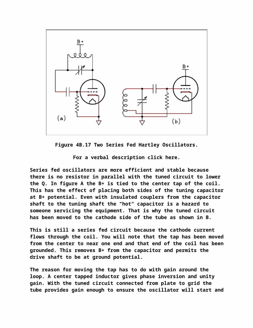
The subject of Boolean algebra is one which could occupy an entire semester. There is not time or space to offer proofs of any of the theorems. The theorems will simply be stated and their applications indicated. The interested reader is referred to texts devoted exclusively to the subject.
Notation.
The functions in Boolean algebra are not the mathematical functions we are accustomed to but are the logic functions of AND, OR, NOT and XOR. The symbols for these functions look like some of our arithmetic symbols but in the context of Boolean algebra they are read differently.
The OR function is symbolized by a plus + sign. Thus C = A + B is not read as "c equals a plus b" but is read "c equals a or b". The table in Figure 8.12 summarizes the Boolean functions and the proper way of speaking each.
The symbol normally used for the exclusive OR function is a plus sign with a circle around it. This symbol is not available in text mode in html. The symbol in text for exclusive OR will be "XOR". In graphics the symbol will be used.
Figure 8.12 Table of Logic Functions and How to Speak Them.
For a verbal description click here.
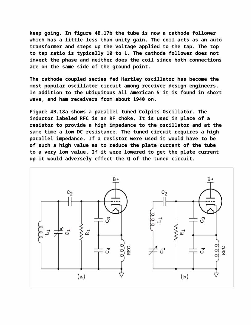
Figure 8.13 Summary of Boolean Algebra Theorems.
For a verbal description click here.
Figure 8.13 lists some of the most important theorems in Boolean algebra. As you look over the table of theorems you will note some similarity to linear algebra. The last entry in the table is called DeMorgan's theorem. It is one of the most powerful and useful theorems for designing logic circuits.
Example 8.2.
Use a truth table to prove that not A and B or A and not B = A X-or B.
Solution:
For a verbal description click here.
QED.
Example 8.3.
Simplify the following Boolean expression.
Solution:
Factoring out an A we have
Using the theorem proven in Example 8.2 yields
8.4 Combinational Logic Circuits.
The term combinational logic is applied to any connection of logic gates which serves some specific purpose. For example, suppose that there is an experiment in which something in the apparatus could be damaged if certain switches were to be on at the same time. A system of gates could be used to shut down some critical part of the setup if an operator accidentally set the forbidden combination.
Suppose that the equipment may be damaged if switches A and C are on at the same time or if switch B is off when switch D is on. The protection circuit P must be activated if A and C or not-B and D are on. In Boolean form the equation is,
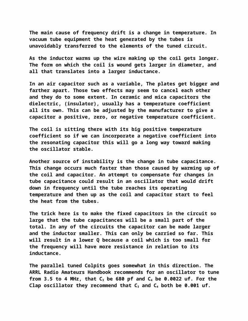
Expression 8.1 cannot be simplified further. The circuit is shown in Figure 8.14. Gate 1 inverts the B input to form not B. Gate 2 forms the A AND C term while gate 3 forms the B AND D term. Gate 4 forms the final output.
Figure 8.14 Realization of Boolean Expression 8.1.
For a verbal description click here.
It was mentioned earlier that DeMorgan's theorem is very useful in creating logic circuits. The reason is this. The easiest type of gate for IC designers to design and manufacturers to make is the NAND gate. This is true for both TTL and CMOS logic families.
Suppose that it is necessary to implement the following Boolean expression:
The first impulse would be to use the circuit of Figure 8.15a. However, DeMorgan's theorem extended for three variables states that,
The expression D = not the quantity A X B X C may be implemented with a single 3 input NAND gate as shown in Figure 8.15b.
Figure 8.15 DeMorgan's Theorem Is Used to Simplify Circuits.
For a verbal description click here.
The entire process of logic design is to start with a Boolean expression, simplify it and get as many NAND functions in it as possible, then convert the expression to a circuit.
Example 8.4.
The output of a logic circuit is to be high (on) if A is on and B and C are off, or if A and C are on and B is off. Write the Boolean expression, simplify it if possible and then draw the circuit.
Solution:
The initial form of the expression is
If we factor out an A and not B from each term we have
but not C or C = 1 and A and 1 = A; therefore, D = A and not B. The first impulse is to use an inverter to obtain the NOT-B term and a two input AND gate. Something you may not know is that gates do not come one per package. Two input gates come four per package. (The term DIP is often used. DIP stands for Dual Inline Package.) A two input NAND gate may be used as an inverter by tying its two inputs together and using them as the inverter's input. We can use one of the NAND gates as an inverter to obtain the NOT-B term, use another to perform the NAND function of A NAND NOT-B and then use another inverter to invert the output of the NAND gate and thereby convert it into an AND gate. The circuit is shown in Figure 8.16.
Figure 8.16 Solution to Example 8.4.
For a verbal description click here.
The initial uninformed solution might have been to implement the logic circuit based on the description in the example. A little Boolean algebra showed that the C input was redundant. In a simple circuit this wouldn't have made any practical difference. In a very complex circuit a redundant input could lead to use of a lot of unnecessary parts.
The solution to Example 8.4 ended up using three of the gates in a quadruple 2 input NAND gate. Such an IC costs less than 25 cents in TTL and less than 50 cents in CMOS.
Combinational logic circuits can get very complex as can the Boolean expressions which represent them. Such large projects are the province of design engineers who are experienced in such matters. The physics student should only attempt to design logic circuits if they are small and simple, as in Example 8.4.
8.5 Flip-Flops and Counters.
The formal name for a flip-flop is a bistable device. It is a device which is stable in either of two states and will remain in whichever state it is in until it is forced into the other state where it will remain until again changed. Although this definition sounds simple, flip-flops come in a wide variety of shapes, sizes and colors. We will begin with the simplest.
Switch Debouncing Flip-flop.
We are accustomed to thinking of mechanical switches as being either on or off. But if you look on a microsecond time scale, when a switch is turned on or off the contacts open and close several times before they finally settle down to the state in which it has been placed. If the switch is being used to turn a flashlight on and off the bouncing will make no difference and will not even be detectable by the user. But if the switch is being used to activate a logic circuit, operating the switch once may make the logic circuit "think" that the switch has been operated several times. The circuit of Figure 8.17 employs two NAND gates to generate one state change for each position change of the switch.
Figure 8.17 Switch Debouncing Circuit.
For a verbal description click here.
Suppose that the switch has just been thrown and is in transition between the two contacts. Neither switch contact is connected and so both switch contacts are pulled up to VCC by the 10 k ohm resistors. Suppose that Q is low (logic 0) and NOT-Q is high (logic 1). Both inputs to the upper gate are high which allows its output to be low. The lower gate has one input high and the other one low which makes its output high. So far so good, no contradictions.
If the grounded swinger of the switch makes contact to the upper contact, one of the inputs to the upper gate will be pulled low. That will force its output to go high. The lower gate will now have a high on both inputs, which will make its output low. Thus, NOT-Q will be low (0). If the swinger loses contact on a bounce, the two outputs will remain in the same state. The swinger may bounce on the upper contact as many times as it likes, the state of the flip-flop consisting of the two gates will not change again until the swinger touches the lower contact.
Each time the switch is changed to the other position, the state of the flip-flop is changed by the first bounce of the switch contact. Subsequent bounces will not affect the state of the flip-flop. The contact will not bounce far enough to touch the other contact. The contacts are not made of rubber.
The R-S (Reset Set) Master-slave Flip-flop.
The logic diagram of an R-S master-slave flip-flop is shown in Figure 8.18. If the Ck (clock) input is low, gates 1 and 2 will both have high outputs and the master flip-flop consisting of gates 3 and 4 will remain in whatever state it was in; the states of the R and S inputs will have no effect on gates 3 and 4. If the Ck (clock) input is high, gates 1
Figure 8.18 Internal Logic Diagram of an R-S Flip-flop.
For a verbal description click here.
and 2 will be open, which means that the states applied to R and S will be transferred into the master flip-flop. The high on Ck will be inverted by the inverter and gates 5 and 6 will have low states on their inputs, which will close these gates. The outputs of gates 5 and 6 will be high, which means that the slave flip-flop will remain in whatever state it was in.
It may seem impossible to ever transfer a logic state from the R and S inputs to the Q and NOT-Q outputs. Of course it is possible or the circuit would be useless. Let us start out by assuming that the Q output is low. Naturally the NOT-Q output is high. Referring to the flip-flop as a whole it is said to be in the zero state. Let us say that the S input is high, the R input is low and the Ck input is low. Because Ck is low the outputs of gates 1 and 2 will be high. The output of gate 3 must be low and gate 4 high. Gates 5 and 6 are open and these states are transferred through to gates 7 and 8. Now when the Ck input changes to high, gates 1 and 2 are opened and the states on R and S are inverted and transferred to the inputs of gates 3 and 4. A low on one of the inputs of gate 3 will cause its output to go high and gate 4 will have both of its inputs high, which will make its output low. The master flip-flop is now in the 1 state. With the Ck input high, gates 5 and 6 are closed and the slave flip-flop remains in the zero state. When the Ck input changes back to the low state, gates 1 and 2 are closed and the master flip-flop cannot be any further affected by the states on the R and S inputs. The level shift causes the inverter to change states at a lower voltage than gates 1 and 2. On a negative transition, gates 1 and 2 are closed before gates 5 and 6 are opened. Thus there is an approximate 20 nanosecond period when both sets of gates (1 and 2) and (5 and 6) are closed and the R and S inputs are never connected directly to the Q and NOT-Q outputs. With the Ck input in the low state, gates 5 and 6 are opened and the 1 state of the master flip-flop is transferred into the slave flip-flop. Thus the state of Q is now high and NOT-Q is low. If the S input is high and R is low the flip-flop will be Set to the 1 state (Q high and NOT-Q low) and when R is high and S low the flip-flop will be Reset to the zero state. The states of Q and NOT-Q will change only when the Ck input changes
from high to low. After the states of Q and NOT-Q have changed to match the states of S and R, additional clock transitions have no effect on the state of the outputs.
If R and S are both low, the flip-flop will remain in its previous state. The outputs will not change states on the clock transition. If both R and S are high, the flip- flop of gates 3 and 4 will be forced into an undefined state and when the clock goes low it will be released from that state and will randomly fall into one of its two stable states. The ending state cannot be predicted. A given IC may always fall into the same state but a different IC may always fall into the other state. Yet another IC may randomly fall into one or the other state.
Most flip-flop ICs have direct set and clear inputs. These inputs will override all other inputs and force the flip-flop into the 1 (set) of 0 (clear) states. The logic involved makes the circuit look more complicated because of the increased number of inputs to gates 3, 4, 7 and 8. A student with a firm grasp of the subject of logic could figure out how to add direct set and clear to this circuit.
The J-K Flip-flop.
If the R-S flip-flop is cross wired (Q to R and NOT-Q to S) an interesting thing happens. Suppose that the flip-flop is in the zero state (Q = 0 and NOT-Q = 1). This means that S has a high applied and R has a low. When a negative edge of the clock occurs, the flip-flop will be loaded with a 1. Following the negative-going clock the R input has a high applied and the S has a low applied. On the next negative-going clock edge the flip-flop will be loaded with a zero. The flip-flop will change its state on every negative-going edge of the clock signal.
Now the importance of the level shift becomes evident. On a positive edge of the clock, gates 5 & 6 are closed before gates 1 & 2 are opened. On a negative edge gates 1 & 2 are closed before 5 & 6 are opened. If the R and S inputs were to be connected directly to the outputs even for a few tens of nanoseconds the circuit would most likely oscillate and the ending state would be completely random.
Figure 8.19 Internal Logic Diagram of a J-K Flip-flop.
For a verbal description click here.
If we make gates 1 and 2 into 3 input gates we have a J-K flip-flop as shown in Figure 8.19. The J-K flip-flop behaves differently from the R-S flip-flop in regard to what happens when J and K are high. In an R-S flip-flop when R and S are high the result is unpredictable. In a J-K flip- flop when J and K are high the flip-flop will change states on every negative edge of the clock input. The process of changing states on every clock is often called toggling. A flip-flop which has been permanently wired to change states on every clock pulse is often called a toggle flip-flop.
If J is high and K is low the flip-flop will be set to the 1 state on the next negative edge of the clock. If J is low and K is high the flip-flop will be set to the zero state on the next negative edge of the clock. If both J and K are low the state of the flip-flop will remain unchanged.
The Type-D (Data Storage) Flip-flop.
In order to store a bit (binary digit) in an R-S or J-K flip-flop it is necessary to place one of the inputs high and the other one low. Since the two inputs are always in opposite states the natural thing to do is to connect an inverter in the circuit as shown in Figure 8.20a. When a flip-flop has been internally wired in this way it is symbolized as in Figure 8.20b. Notice first of all that the internal logic diagram has been replaced by a rectangle. If a logic high (1) is placed on the D input, the next negative edge will cause the flip-flop to assume the 1 state (Q = 1 and NOT-Q = 0). If a logic low (0) is placed on the D input, the next negative edge on the clock will cause the flip-flop to assume the zero state (Q = 0 and NOT-Q = 1). Once the data bit has been stored in the flip-flop, subsequent clock pulses will just keep loading the same data again and again. If the data does not change between clock pulses the state of the flip-flop will not change.
Figure 8.20 D-type Flip-flop from J-K Flip-flop.
For a verbal description click here.
The Cl connection at the bottom of the rectangle and the S connection at the top are direct clear and set inputs respectively. This S is not the same as the S input on an R-S flip-flop. Clear and set inputs are usually active low, which means they are normally high and to clear the flip-flop the Cl input should be pulled low for a few tens of nanoseconds. To set the flip-flop the S input should be pulled low. In the case of TTL an input which is left open will automatically go high. A CMOS input should never be left open; on a CMOS flip-flop the Cl and S inputs must be tied to VCC through either a wire or a 10 k ohm resistor.
Binary Counter.
Figure 8.21 shows the diagram and truth table for a 4-bit binary counter. There is an inherent conflict between the way we draw circuits and the way we write numbers. The standard way of drawing circuits is to have the signal flow from left to right. That places the least significant bit on the left. The way we write numbers is to have the least significant bit on the right. This contradiction cannot be defined away. We must simply live with it.
The input to the counter may be irregular or regular pulses as indicated along the top of the figure. All unconnected inputs to the flip-flops are assumed to be logic high. Every time a flip-flop receives a negative-going edge, its state will change. See the table in the figure.
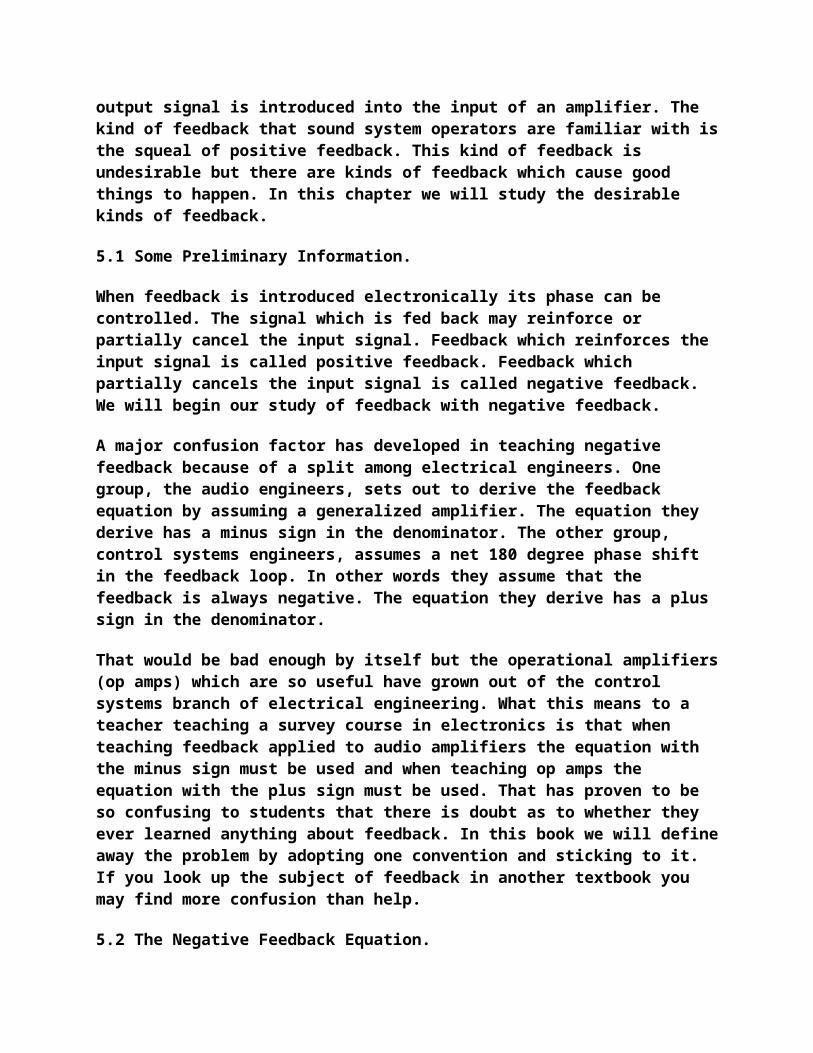
Figure 8.21 4-Bit Binary Counter and Its Truth Table.
For a verbal description click here.
Every time the input changes from high to low, flip-flop A will change states. Every time flip-flop A changes from a 1 to a 0, flip-flop B will change states and so on. If the counter starts from zero (all bits zero) the count at any time will equal the number of negative edges which have occurred in the input signal. The number is of course expressed in binary. The number of flip-flops in the counter may be arbitrarily large. The largest number NL a given counter can contain is
NL = 2N - 1 (8.4) where N is the number of flip-flops in the counter.
If the input to the counter is a square wave it has a definite frequency. In this event the output of the counter also has a definite frequency. The output frequency is given by
fO = fIN / 2N (8.5) where fO is the output frequency, fIN is the input frequency and N is the number of flip-flops in the counter. Thus we have a means of changing (lowering) the frequency. With a simple binary divider the input frequency may only be divided by 2N where N is an integer.
When a binary counter is used to divide frequencies it is called a frequency divider. Divide ratios can be other than 2N but the circuitry becomes more complex. Noninteger divide ratios are even possible but the circuitry becomes very complex.
Example 8.5.
The input frequency to a 9 stage (9 flip-flops) binary counter is 225,280 hertz. What is the output frequency?
Solution:
fO = fIN / 2N = 225,280 / 29 = 440 hz.
The Decade Counter.
When binary numbers were introduced it was said that it was difficult to make electronic circuits which could count in decimal. In the age of the IC it is easier than it was in the vacuum tube age. Computer hardware designers still prefer to use binary but in stand alone digital instruments such as digital clocks, frequency counters and digital voltmeters the decade counter is king.
The circuit employs a number system known as binary coded decimal (BCD for short). Figure 8.22 shows how to count from 0 to 12 in BCD. Each decimal digit is represented by 4 binary digits (bits). Four bits of binary can normally express numbers as large as 15 (1111) but in BCD the highest allowed count is 9 (1001). Binary counts higher than 1001 are not allowed. Notice that in Figure 8.22 when the units count reaches 9 it resets to 0 and a 1 is placed in the tens column.
This system of counting requires more bits than a comparable binary counter. For example a 3 digit BCD counter can count to 999 and requires 3 digits x 4 bits per digit = 12 bits. A binary counter which can count to 1023 requires only 10 bits. The extra bits are well worth the tiny increase in cost. The circuitry to readout a 10 bit binary counter in decimal is far more complex and expensive than the couple of extra bits required for making BCD counters.
Decimal Tens Units
00 0 0 0 0 0 0 0 0
01 0 0 0 0 0 0 0 1
02 0 0 0 0 0 0 1 0
03 0 0 0 0 0 0 1 1
04 0 0 0 0 0 1 0 0
05 0 0 0 0 0 1 0 1
06 0 0 0 0 0 1 1 0
07 0 0 0 0 0 1 1 1
08 0 0 0 0 1 0 0 0
09 0 0 0 0 1 0 0 1
10 0 0 0 1 0 0 0 0
11 0 0 0 1 0 0 0 1
12 0 0 0 1 0 0 1 0
Figure 8.22 BCD Counting from 0 to 12.
In order to implement BCD in hardware it is necessary to wire together 4 flip-flops in such a way as to count from 0 to 9, which is the same thing as dividing the input frequency by ten. Ten can be factored as 2 x 5. A single flip-flop can handle the divide by 2. Three flip-flops and some gates are used to accomplish the division by 5.
A practical decade counter is made up of 4 flip-flops, as shown in Figure 8.23. This circuit consists of a count- to-one (divide by 2) and a count-to-four (divide by 5) circuit. The count-to-one section consists of flip-flop A. The count-to-four circuit consists of flip-flops B, C, D and two gates.
Whenever a TTL (transistor transistor logic) input is left open, it assumes the high logic state. (This is not recommended in circuits constructed in the laboratory.) The J and K inputs on flip-flop A are open; consequently, they both have high logic states or 1s applied. If a J-K flip-flop has 1s on both J and K inputs, the flip-flop will change states every time the clock input goes from a logic 1 to a logic 0. If there is one cycle at the output for every two cycles at the input, you have a divide by 2 counter.
The divide by 5 is not so simple. If 3 flip-flops are connected with the Q output of one going to the Ck input of the next, the counter will be a count to 7 or divide by 8. To make this counter divide by 5 instead of 8 requires some trickery.
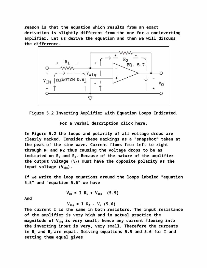
Figure 8.23 Decade Counter and Its Truth Table.
For a verbal description click here.
The truth table which accompanies Figure 8.23 has all of the numbers written backward. This should aid in understanding the circuit. The column of binary digits for a given flip-flop is under that flip-flop.
Starting out with all flip-flops set to zero, the NAND gate will have a 0 and a 1 on its inputs. Its output will be a 1. This 1 when applied to the J input of F-F B will allow it to change states on every clock pulse. When the count in F-Fs B, C and D reaches 0 0 1 (binary 100) both inputs of the NAND gate will be 1s and the output will be 0. The 0 on the J input of F-
F B will prevent it from changing states on the next clock pulse. Because there is no change in the state of F-F B, there will not be any trigger pulse delivered to F-F C and it will remain in the 0 state.
The AND gate gets its inputs from F-Fs B and C. The output of the AND gate will be 0 as long as B or C is 0. The 0 applied to the J input of F-F D will inhibit it from changing states and it will remain in the 0 state. When B and C are both 1s, there will be a 1 on the J input of F-F D and it will change states on the next clock pulse.
Note that the clock pulses are connected to F-Fs B and D. The clock pulse which caused D to change from 0 to 1 will cause B to change from 1 to 0. This change on the Q output of F-F B will cause F-F C to also change from 1 to 0. F-F B is now inhibited from changing states. As we have already seen, F-F D had a 1 on its J input before the clock transition and so the next transition will cause F-F D to change from 1 to 0. We now have all flip-flops back in the 0 state and we are ready for another counting cycle.
This circuit is almost never implemented with separate J-K flip-flops and logic gates. A decade counter integrated circuit is normally used. Different manufacturers implement the counter in different ways and many of them will not even tell us how they do it. It may be done this way or some other way; we don't know.
Variable Modulus Counters.
The modulus of a counter is that number by which it will divide an input frequency. For a counter of modulus N, for every N pulses sent to the counter it will deliver one pulse. The modulus of a 4-bit binary counter is 16, that of a decade counter is 10 and that of the B, C and D flip-flops of a decade counter is 5.
As illustrated by the decade counter it is possible to develop systems of flip-flops and gates to give any desired modulus. Such systems are hard-wired and cannot be changed by the equipment operator. There are counters whose moduli can be changed by the operator.
A very common variable modulus counter uses the up-down decade counter. Each IC has a count-up and a count-down input. There are also carry and borrow outputs. The carry output is wired to the count-up input and the borrow output is wired to the count-down input of the next most significant digit counter. These counters also have a set of direct load inputs which permit data to be loaded into the counter. A "load enable" input on the IC causes data which is presented at the data inputs to be loaded into the flip-flops of the counter.
When the input signal is applied to the count-down input of the least significant digit the borrow output of the most significant digit will go low only when all digits in the counter are zero. The rest of the time this output is high. If this output is connected to the load enable inputs of all of the other digits in the counter the data will be loaded whenever the counter arrives at zero. The data are loaded when the load enable input is low.
The sequence of events is this: the counter counts down to zero, the data are loaded, and the counter counts down to zero again. The modulus of the counter is equal to the number contained in the data which is loaded. If the data are changed, the modulus of the counter is changed.
One way an operator can interact with such a counter is by means of thumb-wheel switches. Each switch has ten positions. When the switch is set to a given position a digit (0 through 9) will show in a window to indicate to the operator the position selected. The switch has four contacts which generate the BCD code corresponding to the digit selected. These switches are designed so they may be placed side by side to allow an operator to set a decimal number on the switches. The outputs of the switches are the BCD code of the number selected. If the switches are connected to the data inputs of the up-down counters, the switches may be used to select the modulus of the counter. The usefulness of such a variable modulus counter will be shown in the next chapter.
It is possible to achieve a noninteger modulus by using combinational logic to set the modulus, as was done for the divide-by-five circuit. Such a circuit may be arranged so that a logic level on one of the gates will change the modulus of the counter. The level on this modulus control input may be rapidly switched to obtain an average modulus which is between integer values. Such a counter must be followed by several divide-by-two flip-flops in order to average out the frequency variations and give a true single frequency output. Circuits of this kind are used in an IC called a "top octave generator". This IC uses a quartz crystal (externally connected) and divides it down to deliver simultaneously all twelve of the musical notes in the top octave of the standard piano keyboard. In each lower octave the frequencies of the notes are half of those in the next higher octave. Simple binary dividers may be used to generate the rest of the notes on the keyboard.
By the way, if you want to amaze a guitar-playing friend by telling him or her the frequencies of the musical notes, it is easy using a calculator. The frequency of the note A above middle-C is 440.000 hz. The notes comprise a geometric series with the twelfth root of two being the factor. Use the YX key on your calculator to raise 2 to the 1/12 power and store the result in memory. Key in 440. To move down the musical scale, recall and divide. To move up the scale, recall and multiply. If you work your way down the scale to middle-C you will find its frequency to be 261.6256 hertz. You may well have read in an elementary physics book that middle-C has a frequency of 256 hertz. The best information available to the writer indicates that musicians changed the standard of tuning sometime early in the 20th century. They forgot to tell the physicists. Meanwhile, any physicists writing a book would look up the frequency for middle-C in the book he had used as a student which was written by someone who looked it up in a book he had used as a student and so on. This is how misinformation can be passed down from one generation to the next.
8.6 Displaying the Count.
In any digital instrument it is necessary for the contents of the counter to be displayed in some way for an operator to read. Figure 8.24 shows the block diagram of a single digit of the readout system for a decade counter.
Figure 8.24 Decade Counter, Latch, Decoder and Display.
For a verbal description click here.
The numbers in the blocks are type numbers of specific ICs. The 7490 is the decade counter. Such a counter is in the middle of a chain of similar decade counters. The 7475 is a 4-bit memory consisting of 4 type D flip-flops. The purpose of the "strobe" input is to cause the data in the decade counter to be loaded into the memory. The purpose of the memory is to remember the count while a new count is being accumulated. The sequence of events is this. The count begins and the decade counters count up from zero. When the count has finished, the "strobe" inputs of all of the memories is pulsed which stores the data in the memory. The counters may then be reset (to zero) and a new count begins while the memory holds the previous count.
The contents of the memory are fed to the 7447 which is a decoder-driver. This IC uses combinational logic to convert the BCD code from the memory to the proper pattern to display numerals on the 7-segment display. The outputs of the decoder-driver are BJTs which are "on" to light a display and "off" to keep it dark. These BJTs are capable of switching enough current to drive almost any display which may be used.
The display itself consists of 7 light emitting diodes (LEDs). These LEDs have an I-V curve similar to any other diode. The full 5 volt power supply cannot be applied across the LEDs in the display. There must be a current limiting resistor in series with each LED in the display. A typical value is 220 ohms. Some other types of decoder-drivers have these resistors built in to the IC.
There must be one of these circuits for each digit to be displayed. An 8-digit display would have eight 7490s, eight 7475s, eight 7447s, fifty-six resistors and eight displays.
8.7 Multiplexed Displays.
The term LSI means large scale integration. It is LSI which has made the pocket calculator possible. One problem with LSI is the number of pins necessary to connect to the display. A ten-digit calculator needs eighty pins to control the numeric display and the decimal points. That is far too many for a reasonable size for the IC and the calculator it is used in.
A way to save pins is to multiplex the display. Instead of connecting the anodes of the LEDs in the display to the +5 volt line, they are connected to the collectors of PNP switching transistors. A ten-digit calculator needs ten control lines, one for each digit. All of the segment cathodes are connected in parallel. For example the top segments in all ten of the digits are connected together. All ten of the decimal point cathodes are connected together. That means that there are 8 lines, one for each segment and 1 line for the decimal points. That makes 10 digit control lines plus 8 segment control lines for a total of 18 lines to control 10 digits, instead of 80 as would be the case for individual segment connections. Also only 8 resistors are needed for current limiting.
The way in which this works is as follows. The PNP transistors in the digit anodes can turn an entire digit on or off. The first digit is turned on (all others are off) and the pattern of bits is applied to the segment lines to display the number in the first digit. The first digit is turned off and the second digit is turned on. The data on the segment lines is changed to that of the number in the second digit. The process repeats until all of the digits have been illuminated and then the process begins again. Even though only one digit is on at a time, the eye perceives a continuous display of all digits. The scanning of the displays may occasionally be observed when a calculator is shown on television. The field rate of the TV scanning may "strobe" with the scanning rate of the calculator's display.
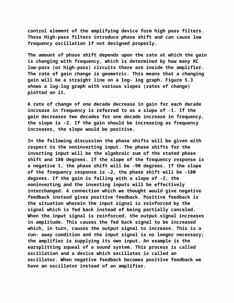
Figure 8.25 Multiplexed 4 Digit Display.
For a verbal description click here.
The display will appear to flicker and if the frequency of the display scanning is just right it may even be seen to scan in order. If you ever gain access to a stroboscope, (not to be confused with a strobe light), you may want to put your calculator under it and see if you can find the scanning frequency.
The keyboard of a calculator s another problem. Many calculators have 40 to 50 keys. If there had to be one pin on the IC for each key, calculators would be a lot larger and more expensive than they are.
The keyboard is divided into rows and columns (not necessarily related to their physical placement on the calculator). The keyboard is scanned. For example a calculator having 64 keys does not need 64 pins to connect the keys. The keyboard is electrically arranged into an 8 by 8 matrix and connected as shown in Figure 8.26. Each switch is a key on the calculator. The calculator IC may send pulses out on the column lines one at a time and monitor the row lines for returned pulses. When a switch is closed only one of the 8 column
pulses will be received and it will be received on only one row line. That gives an unambiguous way for the chip to know which one of the switches was closed. The calculator IC needs only 16 pins for the keyboard instead of 64.
Figure 8.26 Multiplexed Calculator Keyboard.
For a verbal description click here.
8.8 Digital to Analog Converter.
A number held in a digital counter or memory is just a number. Like any number it represents only what we humans imagine. In and of itself it represents nothing. However, a circuit may be constructed which will convert a digital number to a proportional voltage. Such a circuit is called a digital to analog converter (DAC).
A digital to analog converter (DAC) which is easy to understand is shown in Figure 8.27. Suppose that the output of the digital buffers is 5 volts if the input is a logic 1 and zero volts if the input is a logic zero. If the most significant bit (MSB) is 1 the 10 k ohm resistor will supply a current of 0.5 mA to the summing node of the op amp. The next bit will cause a current of 0.25 mA to be delivered to the summing junction, the next a current of 0.125 and so on. If the least significant bit (LSB) is a 1 the current from it is 7.8125 uA. An infinite
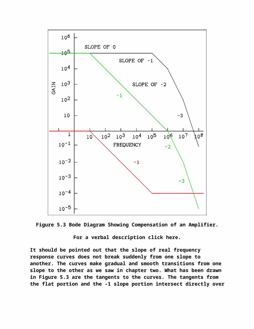
number of bits would bring the total current (all bits on) up to 1 mA. The condition of all bits on (1) is the full-scale condition. The 5 k ohm feedback resistor will cause the op amp to have a full-scale output voltage of -5 volts. When converting binary to decimal each bit has twice the value as the bit to its right. In the case of the digital to analog converter each bit supplies twice the current as the next least significant bit. The op amp causes all of these currents to be summed and converted into a negative voltage. If a positive output is desired another op amp may be connected as a unity-gain inverter.
Figure 8.27 Simple Digital to Analog Converter.
For a verbal description click here.
Although this circuit is easy to understand it doesn't work very well. The problem is the resistors. If the resistors are not exactly right on value the converter will not yield uniform steps as the binary number is incremented. Take the case of stepping from 63 to 64. The number 63 has the 6 least significant bits on. When this number changes to 64, 6 bits turn off and a single bit takes its place. The 10 k ohm resistor must supply a current which is exactly 7.8125 uA larger than the current supplied by the combination of the 6 other resistors. (The smallest possible step in the output of a DAC is the value of the least significant bit.) Errors in resistors are random and, if the particular resistors have errors such that the 20 k ohm is a little low and the 10 k ohm is a little high, incrementing the binary code from 63 to 64 could actually result in a reduction of the output voltage instead of an increase. As the number of bits increases the smallest steps become smaller and the requirements on resistor tolerance become impossibly tight.
Another problem is the wider range of resistor values required by this type of converter. The values in this example circuit range from 10 k ohm to 640 k ohm and this is only a 7-bit converter. A 16-bit converter which has a lowest value resistor of 1 k ohm would have to have a highest value resistor of 32.768 M ohms. Maintaining the necessary tolerances over such a wide range of resistance is impossible.
Figure 8.28 Ladder Network Digital to Analog Converter.
For a verbal description click here.
Figure 8.28 shows a digital to analog converter which will work. The figure shows only 4 bits but the circuit may be extended to as many bits as desired. If the MSB is the only bit to be on, the output voltage will be half of the power supply voltage. That is as it should be because the MSB always represents half of the (largest - 1) number that a given binary number can represent. The MSB is 1/2 scale. The next bit is 1/4 scale, the next 1/8 scale and so on.
Although it is not exactly cheap, it is possible to make a large number of resistors all of the same value. The ladder network is supplied in a package which looks like an IC. The resistors were all made at the same time on a common substrate. The resistors indicated as 2R are just two of the resistors connected in series during the manufacturing process. The actual value R may vary by as much as 10% from unit to unit but within a single unit the resistors are all identical to within a small fraction of a percent. A very high precision DAC may be constructed using a ladder network.
The diagrams show noninverting buffers as the drivers for the DAC. Ordinary TTL cannot be used at all and even CMOS is not good enough for high accuracy DACs. The problem is the voltage that the output of the buffer goes up to when its output is a logic 1. TTL is only guaranteed to go up to 2.4 volts. CMOS does quite a bit better but when its output is loaded by a resistor network the output of a buffer may not make it all of the way to ground for a logic zero or all the way to VCC for a logic 1. Designers of DACs go to great length to design switching circuits which will be at zero volts for a binary zero and at VCC for a logic 1. In addition the VCC supply must be very precisely regulated.
As a physicist you will never have to worry about any of the above. DACs are available in IC form ranging in bit count from 8 to 20 and in price from $3.95 to several hundred dollars. The data sheet for the particular DAC IC to be used must be consulted in order to use it properly.
8.9 Analog to Digital Converter.
The process of converting a voltage to a digital number is called analog to digital conversion. The voltage may be converted to a BCD (binary coded decimal) number as is done in a digital multimeter or to a binary number if the data are to be fed to a computer for processing.
Analog to digital converters (ADCs) like DACs come in IC packages. They are available in two basic forms, slow and less expensive and fast and more expensive. The slow kind are dual slope integrators and the fast are successive approximation type. Both types can be quite accurate.
Dual-slope Integrator ADCs.
The dual-slope converter is most often used in digital multimeters. Its output is usually in BCD form for easy decimal readout. The typical speed for this converter is about 4 samples per second. That is plenty fast enough for a slow human to take in.
In the circuit of Figure 8.29 the input voltage must be negative. In a complete voltmeter there are circuits which allow the input voltage to be positive or negative. A flip- flop indicates the polarity of the input voltage. To show this extra circuitry would add to the circuit complexity while adding nothing to the reader's understanding.
Figure 8.29 Dual-slope Integrator ADC.
For a verbal description click here.
In the circuit of Figure 8.29 the switches S1, S2 and S3 are not mechanical but electronic switches which are controlled by the block labeled "control logic". The sampling cycle starts by closing switch S1 to discharge the capacitor. S1 is opened and S2 is closed which signals the beginning of time period T1. The output voltage of the integrator begins to go positive because the input voltage is negative. The slope of the line is determined by the magnitude of the input voltage as indicated by the waveform drawings in the figure. At the end of T1 the output voltage of the integrator is proportional to the magnitude of the input voltage. At the end of T1 S2 opens and S3 closes, signaling the start of T2. The reference voltage is the negative of the full-scale voltage of the converter. When T2 begins, the control logic opens the AND gate by placing a logic 1 on the lower input. The upper input of the gate already has a 1 on it from the output of the comparator.
The symbol for a comparator looks like an op amp and there are similarities. A comparator is a device which can have an analog input and a digital output. It may be thought of as a one-bit analog to digital converter. If the noninverting input is more positive than the inverting input the output will be a logic 1. If the inverting input is more positive than the noninverting input the output will be a logic zero.
In the circuit of Figure 8.29 the inverting input of the comparator is grounded and the positive output of the integrator is applied to the noninverting input. The output of the comparator is a logic 1. Clock pulses from the clock are now passed to the counter. The
counter counts clock pulses for the duration of T2. The time period T2 ends when the output of the integrator reaches zero. As the two different waves in the figure indicate, the higher the magnitude of the input voltage the longer T2 is and the larger the number of clock pulses counted. When the output of the integrator reaches zero the AND gate is closed because the output of the comparator has switched to a logic zero. The control logic is also notified and it initiates a number of steps. S3 is opened, the contents of the counter are loaded into the display memory and the counter is reset to zero. Now S1 is closed and the entire cycle starts over again.
You may be thinking that a much simpler way would be to let the reference voltage be integrated until it equals the input voltage and let the counter count clock pulses during this time. If you did think of this method, go to the head of the class. It shows that you are thinking. The calibration of such a single-slope integrator is very dependent on the value of the capacitor. Capacitors have a rather bad habit of changing capacitance as temperature changes. In a dual-slope integrator the capacitor is used twice and errors in the value of the capacitor are partially canceled out. This partial error cancellation is the primary reason for using a dual-slope integrator instead of a single slope integrator.
Successive Approximation ADC.
Successive approximation converters are very fast, ranging in speed from several hundred samples per second to several million samples per second. In bit count they range from 8 to 20 and in price from $3.95 to several hundred dollars. Because of their great speed they are most often used in association with microprocessors. They usually have binary output.
The diagram of a successive approximation ADC is shown in Figure 8.30. You will notice that contained within the analog to digital converter (ADC) is a digital to analog converter (DAC). The comparator compares the output of the DAC with the input signal and sends its output signal to the control logic. The wide lines on the diagram labeled "data bus" and "control bus" are a shorthand way of drawing many individual connecting lines. In the case of a 16 bit converter, there would be 16 lines connecting the control logic block to the binary register and 16 lines connecting the binary register to the DAC. It is pointless to draw 16 lines when everyone knows that they are all going to the same place.
Figure 8.30 Successive Approximation ADC.
For a verbal description click here.
One very simple way in which this circuit could be used is to start the binary register (used as a counter) at zero, count up until the comparator changes states and then stop. That method works fine provided you are not in a hurry. If the input signal is near full-scale, as many as 65 thousand clock pulses would be required to complete a conversion in a 16 bit converter. The conversion time is dependent on the magnitude of the input signal. An input signal which is near zero takes fewer clock pulses and, therefore, less time than an input signal which is near full-scale.
The successive approximation system works much faster. The difference between a binary counter and a binary register is that a binary register can be loaded with data in many ways. In the binary register used here each bit can be changed individually. The binary register starts with all bits set to zero. The control logic sets the most significant bit (MSB). If the comparator changes states because the output of the DAC is larger than the input signal, the bit is reset. Otherwise it is left set. The next least significant bit is tried in the same way: if turning it on makes the output of the DAC greater than the input the bit is turned off, if the DAC's output is less than the input, the bit is left on. If it is necessary to turn a bit off the same clock pulse which turns that bit off can turn on the next bit. In the case of a 16 bit converter only 16 clock pulses are required to complete a conversion.
A microprocessor could easily be programmed to perform the function of the control logic. A microcomputer which is equipped with a DAC for the purpose of playing music needs only the addition of a comparator feeding into a game paddle port and it can be used as an ADC.
Single IC converters use combinational logic to accomplish the job of the control logic. Such converters can be made very fast indeed.
8.10 The 555 Timer.
The 555 timer resides in a kind of twilight zone between analog and digital. It incorporates elements of both but it is more digital than analog so it is included here.
A 555 timer is basically a monostable Multivibrator or one shot. In this device it is stable in one state where it remains until triggered. Upon being triggered it changes to the other state where it remains for a length of time determined by an RC time constant and then returns to the stable state. Both the TTL and CMOS logic families have one shots in the line. Some are retriggerable which means that if another trigger pulse arrives before the RC has timed out the time period will start over. Others are not retriggerable which means that trigger pulses are ignored while the RC is timing out. Some can be wired for either kind of behavior.
A 555 is not retriggerable and requires the addition of an external transistor to make it into one. The internal block diagram is shown in figure 8.31. Figure 8.32 shows a 555 timer wired as a one shot.
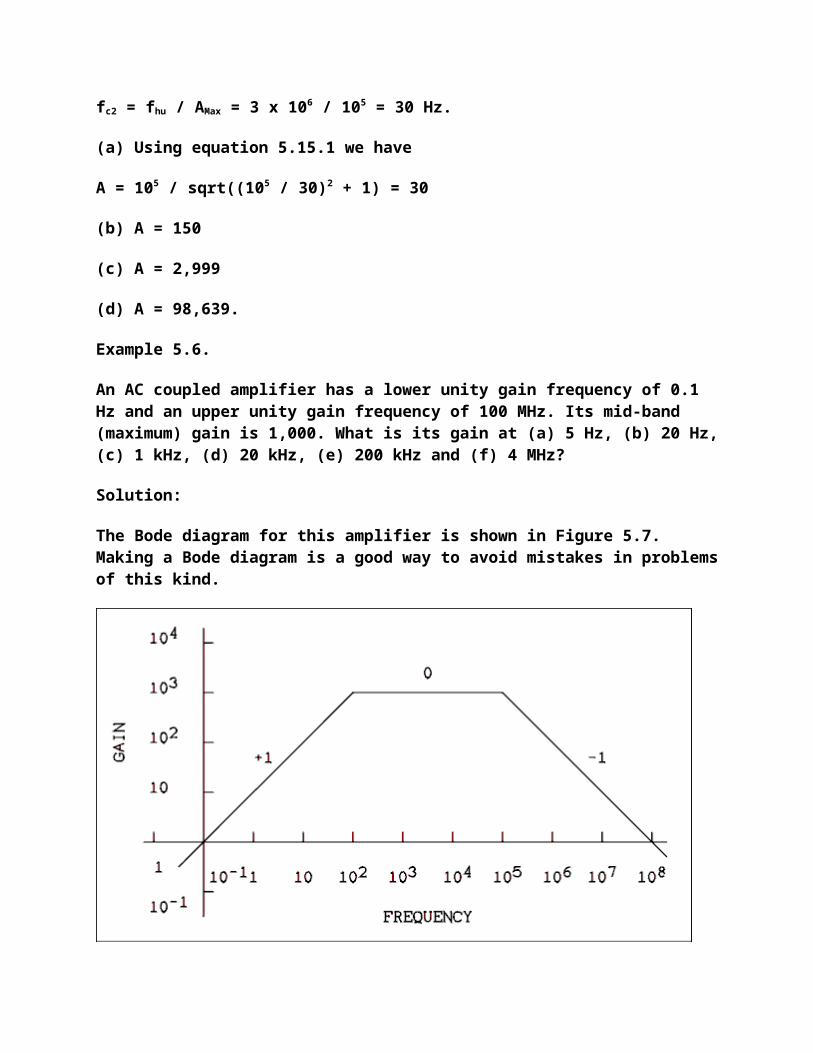
Figure 8.31 Internal Block Diagram of the 555 Timer.
For a verbal description click here.
Figure 8.32 One-shot, Pulse Stretcher.
For a verbal description click here.
In the stable state the trigger input is held high by the resistor. The output is low and the not Q input is high. This holds the transistor on which keeps the capacitor discharged. The trigger input goes to the inverting input of the comparator so the S input of the flip flop is low. The discharge and threshold pins are tied together so the noninverting input of the other comparator is low making the R input of the flip flop low. With R and S both low the flip flop will not change states.
The trigger pulse would be negative and short. A negative pulse on the inverting input of the comparator drives the output positive setting the flip flop. The not Q goes low and the output goes high. The discharge transistor is turned off and the capacitor begins to charge through the resistor. Note the network of equal value resistors in the center. The comparator on the right has its noninverting input held at 1/3 of VCC. The one on the left has its inverting input held at 2/3 of VCC. As long as the voltage across the capacitor is less than 2/3 VCC The R input of the flip flop remains low. When the voltage reaches 2/3 VCC the R input goes high and the flip flop is reset. The output returns to low, the discharge transistor is turned on, discharging the capacitor and the timer is back in its stable state.
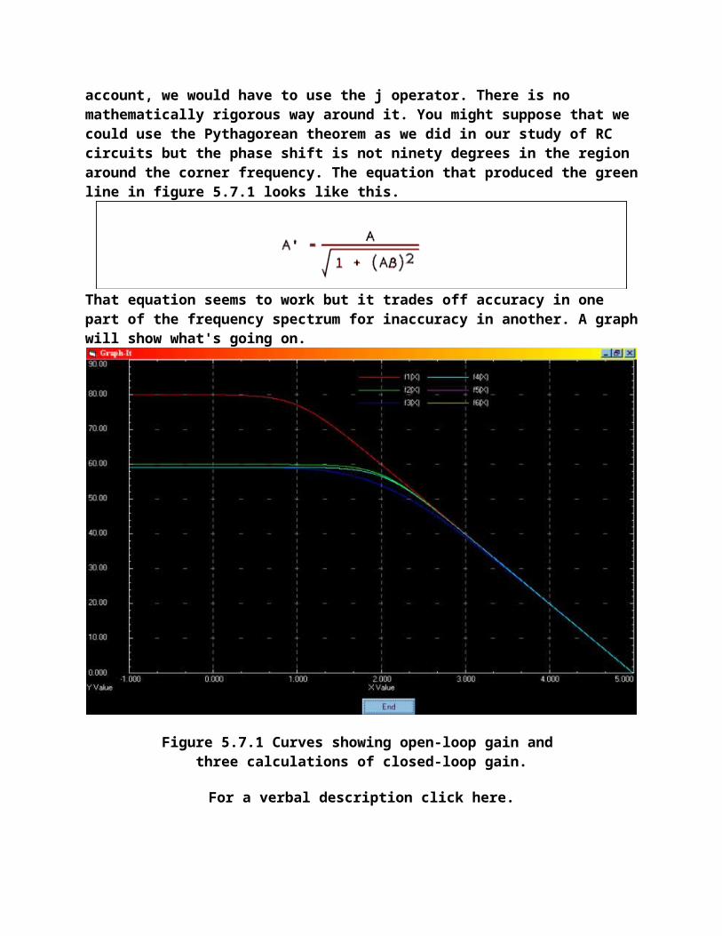
After the timer has been triggered and before the RC circuit has timed out additional trigger pulses will have no effect. Such pulses would set the flip flop but it is already set.
There are many possible uses of this circuit but one could be as a pulse stretcher to turn on an indicator light. Suppose part of an experiment delivers pulses that are so short that even if they were used to turn on an L E D the flash would be too short to perceive. A requirement is that the operator must know when such pulses occur. The narrow pulses could be applied to the input of a circuit like that of figure 8.32 with its R and C values selected for a timeout of say 1 second. The timer could be used to light a lamp and sound a buzzer to be sure to get the attention of the operator.
The time that the output remains high is given by,
T = 1.1 R C (8.6)
Oscillator Circuit.
In the circuit of figure 8.33 The capacitor is connected back around to the trigger input so the timer will trigger itself. There is a resistor connected between the capacitor and the discharge terminal so the capacitor will take some time to discharge.
When the output goes low and the discharge transistor is turned on the capacitor discharges through R2. When the capacitor voltage reaches 1/3 VCC the flip flop is set and the discharge transistor is turned off. The capacitor then charges through the series combination of R1 and R2. When the voltage reaches 2/3 VCC the flip flop is reset and the cycle starts over.
It is impossible to get square waves out of this circuit because the capacitor is charged through 2 resistors in series and discharged through one. The Frequency is given by,
f = 1.46 / [(R1 + 2R2 )C] (8.7)
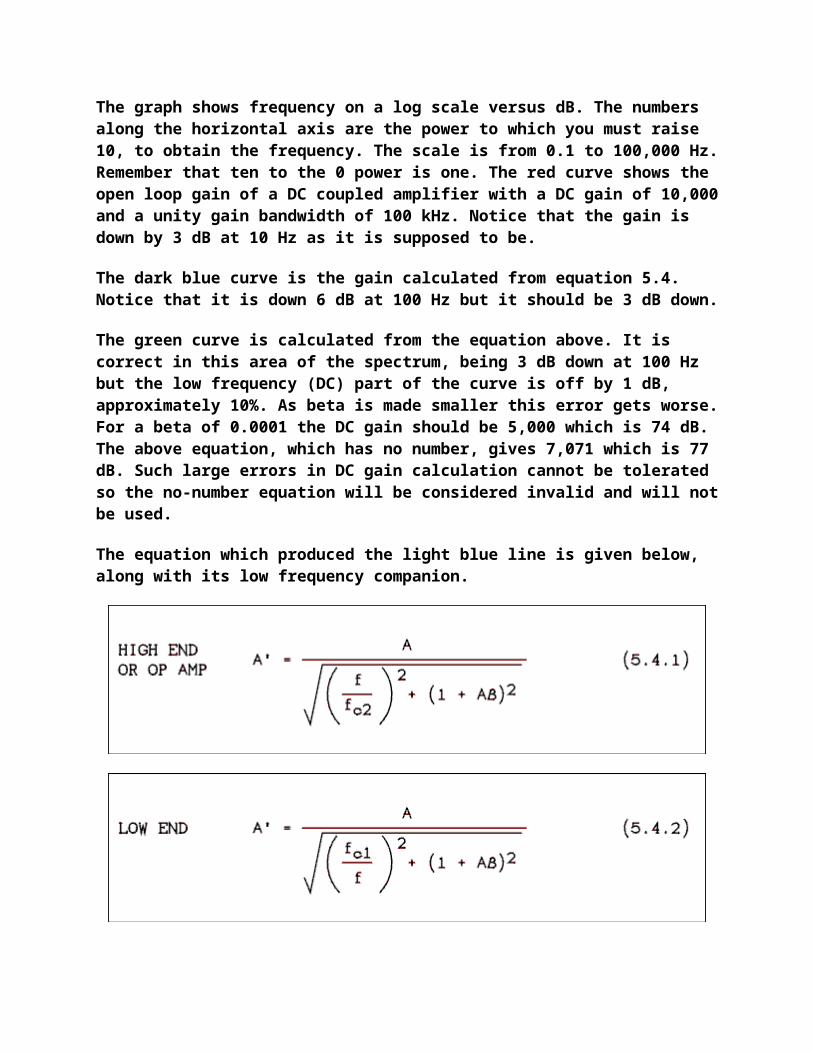
Figure 8.33 Oscillator with Pulse Train Output.
For a verbal description click here.
Figure 8.34 Oscillator with Square Wave Output.
For a verbal description click here.
The circuit of figure 8.34 will solve this problem. When the capacitor is charging the diode effectively shorts out R2, causing the capacitor to charge through R12 alone. If the circuit is operated from 5 volts it will most likely be necessary to make R1 one 5% step less than R2 to account for the effect of the forward voltage drop across the diode. If the resistors are the same value the frequency is given by,
f = 0.730 / RC (8.7)
8.11 Problems.
1. Convert 1110111 to decimal. 2. What is the sum of 101011 and 1101? 3. What are the names of the gates whose truth tables are given here?
4. Write the truth table for the circuit of Figure 8.35. Suggestion: Make columns in your truth table for the outputs of gates 1, 2 and 3. These tree columns will then be the inputs for gate 4.
Figure 8.35 Combinational Logic Circuit For Problems 4 and 5.
For a verbal description click here.
5. Write the Boolean algebra expression for the circuit of Figure 8.35. Do not attempt to simplify it.
6. Convert Expression 8.1 into NAND gates. 7. Reduce the expression below to all NAND functions.
(a)
A B C OUTPUT
0 0 0 1
0 0 1 1
0 1 0 1
0 1 1 1
1 0 0 1
1 0 1 1
1 1 0 1
1 1 1 0
(b)
A B C OUTPUT
0 0 0 1
0 0 1 0
0 1 0 0
0 1 1 0
1 0 0 0
1 0 1 0
1 1 0 0
1 1 1 0
8. Add direct Set and Clear inputs to the master-slave R-S flip-flop of Figure 8.18. Tell what the states of these inputs must be for normal operation and what state will cause a set or clear. You may add inputs to any of the gates if necessary.
9. What is the largest number that a 13-bit binary counter can contain? Express your answer in decimal without using exponents.
10. If the input frequency to a 12-bit binary counter is 3,579,545 hz, what is the output frequency?
11. A frequency divider consists of a divide by 5 module followed by a divide by 7 module which is followed by a divide by 13 module. What is the division ratio of the entire system?
12. In an 8-digit frequency counter the decimal points are to be turned on and off by circuitry within the counter chip. If the display is multiplexed, how many pins are required to connect the display to the counter IC?
13. When a 555 timer is used as a monostable what should be the value of C to give a 1 second pulse if the resistor is 150 k ohms?
14. When a 555 timer is used as an oscillator without a diode what should be the value Of the capacitor to give a frequency of 1 hertz if R1 = R2 = 220 k ohms?
15. When a 555 timer is used as an oscillator with a diode what should be the value Of the capacitor to give a frequency of 1 hertz if R1 = R2 = 330 k ohms?
8.12 Answers to Problems.
1. 119 2. 111000 3. (a) NAND, (b) NOR. 4. Truth table.
A B C OUTPUT
0 0 0 0
0 0 1 1
0 1 0 0
0 1 1 0
1 0 0 1
1 0 1 0
1 1 0 0
1 1 1 1
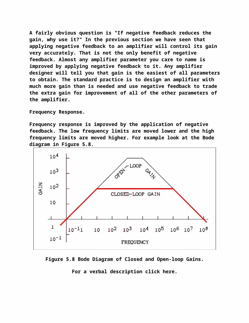
5. The unsimplified expression is,
For a verbal description click here.
6. The NAND gate expression is,
For a verbal description click here.
7. The answer is...
For a verbal description click here.
8. For normal operation both SET and CLR must be high. Pulling the SET input low will set the flip flop and pulling the CLR input low will clear it.
For a verbal description click here.
9. 8191.
10. 873.912 Hz. 11. 455 12. 16. 13. 6.06 micro farads. 14. 2.21 micro farads. 15. 2.21 micro farads.
This page copyright © Max Robinson. All rights reserved.
Digital Instruments. Chapter 9
Frequency 9.1 Counter. Digital 9.2 Multimeter. Frequency 9.3 Synthesizer. Problems. 9.4 Answers to 9.5 Problems.
Chapter 9Digital Instruments.
If you were asked to name something in which digital circuits are used you would likely answer "a digital computer". Combinational logic is certainly used in a digital computer. The subject of computers is one which can occupy a course of its own. There is not time or space here to study computers. There are certain laboratory instruments which employ digital circuitry but which are not computers. These instruments do not require connection to a computer for operation and so are called "stand alone" digital instruments. Three examples which we will look at in this chapter are the frequency counter, the digital multimeter and the frequency synthesizer.
9.1 Frequency Counter.
Figure 9.1 is the block diagram of a basic frequency counter. This circuit is not intended as a construction project. If you were inclined to build a frequency counter, you would need more details. This circuit contains all of the essential parts for understanding the operation of a frequency counter.
Figure 9.1 Basic Block Diagram of a Frequency Counter.
For a verbal description click here.
The input feeds to a buffer which is a circuit with a high input impedance and a low output impedance. This is an analog amplifier circuit which must have a bandwidth equal to that of the counter circuits. The buffer may or may not have a voltage gain greater than unity.
After the input signal is buffered and possibly amplified, it is necessary to form it into a succession of logic highs and lows to be counted by the BCD counters. What must be done is to form the input signal into a square wave which has a low level of 0 volts and a high level of 5 volts. A comparator might be used for this purpose but there is a problem. Noise is always present. A comparator will amplify the noise and instead of a clean square wave its output would be a wave which looks to be a square wave but a closer look reveals that instead of one transition, the voltage makes several jumps from 0 to 5 volts and back again, before settling down on one or the other. Logic circuits respond so fast that they would count these extra transitions as if they were cycles of the input signal. The result would be that the counter would read several times the actual frequency.
The device which is required is called a Schmitt trigger. To explain what a Schmitt trigger does let us look at a specific example, namely the TTL Schmitt trigger. The specifications for such a circuit give its "positive-going trigger voltage VT+" as 1.7 volts and its "negative-going trigger voltage VT-" of 0.9 volts. Suppose the input voltage starts out at zero. Because the circuit is an inverter, the output will be a logic high. As the input voltage is slowly increased, nothing happens until the input voltage reaches 1.7 volts. At this input voltage, the output suddenly switches (in about 20 ns) to a logic low. Further increases in the input voltage have no additional effect. As the voltage is slowly decreased the 1.7 volt point is crossed without anything happening. Nothing happens until the input voltage gets down to 0.9 volts at which point the output switches to a logic 1. As long as the peak-to-peak amplitude of the noise is less than 0.8 volts the output of the Schmitt trigger will

switch only once for each slope of the input wave. The resulting output is a clean square wave.
There are also Schmitt triggers in the CMOS logic family. For these VT+ = 2/3 VCC and VT- = 1/3 VCC. The difference between VT+ and VT- is called the hysteresis of the Schmitt trigger. If the input voltage is between VT+ and VT- the state of the output depends on whether the voltage came down from above or up from below. In other words the state depends on the history of the circuit. Hence the name hysteresis.
CMOS has a larger hysteresis than TTL and, therefore, greater immunity to noise. However, CMOS is not as fast as TTL, which means that it will not count as high a frequency as will TTL.
The next item in the diagram is a NAND gate. Now a NAND gate is just a NAND gate but the other signal to the gate requires some explanation. First of all remember that A NAND 0 = 1 and A NAND 1 = A. Inverting the signal will not change its frequency. When the signal from the flip-flop is 1 the input signal is passed to the counter circuits and when the signal from the flip-flop is 0 the gate is closed and the input signal is not passed to the counter circuits.
The 1 MHz quartz crystal oscillator gives a very precise frequency. This frequency is divided by 1,000,000 to give a very precise 1 hertz frequency. The flip-flop has its J and K inputs high and so will change states on every negative-going edge of the clock input. Thus the Q output will be high for 1 second and low for 1 second. The counter circuits count the total number of cycles and the gate is open for precisely 1 second; so the counter is indicating the number of cycles per second, which is the frequency in hertz.
The not Q output of the flip-flop is fed to the counter circuits and signals when to load the count into the display memory and reset the counter to zero. The not Q signal is not used directly for strobe and reset. It is used to trigger delay circuits, one shots, which perform the strobe and reset in the proper time sequence.
The time that the gate is open does not have to be 1 second. It could be 0.1 second or 0.01 second or anything else. Most counters have a switch to allow the user to select the desired gate time. The proper decimal point lights up in the display along with an additional indicator to tell the user whether the number should be interpreted as hertz, kilohertz or megahertz.
The reasons for having different gate times are resolution and sample rate. If a 1 second gate time is used the reading will be to the nearest hertz which is the resolution of the reading. In some measurements the user may not desire to know the frequency to such precision. The frequency source may be so unstable that the units of hertz are a random number generator. In such cases it is usual to use a shorter gate time to get rid of the insignificant digits of the reading. A shorter gate time gives faster readings. A gate time of 10 seconds gives 0.1 hertz resolution but gives a reading every 20 seconds. A 1 second gate gives a reading every 2 seconds and a gate time of 0.1 second gives 5 readings per second.
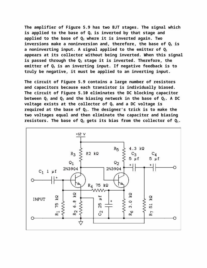
The gate time chosen depends on how much precision is desired and how impatient the user is.
9.2 Digital Multimeter.
The digital multimeter (DMM) uses a combination of digital and analog circuits to measure voltage, current and resistance with great accuracy. All of the individual circuits have been discussed earlier in this text.
The basic measurement circuit of a digital multimeter is the dual slope integrator, which is a voltage measuring device. In most DMMs (digital multimeters) the basic voltmeter circuit has a full-scale range of 0.2 volts (200 millivolts). Voltage dividers are used to give additional ranges of 2, 20, 200 and 2,000 volts full-scale.
For measuring current a series of shunt resistors is connected across the basic voltmeter. The usual ranges are 200 uA, 2 mA, 20 mA, 200 mA and 2 A. Some DMMs have a 20 amp range as well.
AC voltage and current may be measured using most DMMs. An absolute value amplifier is used to convert the basic DC voltmeter to a basic AC voltmeter. An RC network is used as an averaging circuit and so the voltmeter is an average responding voltmeter. The gain of the amplifier is adjusted so the meter will indicate RMS if the input is a sine wave.
More recent DMMs employ a true RMS circuit to convert the AC to DC. When using such meters the reading will always be true RMS regardless of the wave form.
In order to measure resistance the basic DC voltmeter is used to measure the voltage across the unknown resistor while a constant current source supplies current to the unknown. The usual ohmmeter ranges are 200 ohms, 2 k ohms, 20 k ohms, 200 k ohms, 2 M ohms and 20 M ohms. For each of these ranges the value of the current source will be 1 mA, 100 uA, 10 uA, 1 uA, 100 nA and 10 nA, respectively.
9.3 Frequency Synthesizer.
Some types of laboratory measurements require a very stable and accurate frequency. Quartz crystal oscillators provide very stable and accurate frequencies but the frequency is determined when the crystal is manufactured and, if it is desired to change the frequency, a new crystal must be ordered.
There are various oscillator circuits whose frequencies can be varied by means of variable resistors, capacitors, or inductors, but variable frequency oscillators (VFOs) are not as stable over time as quartz crystals. If accurate frequency settings are desired, a frequency counter must be used in conjunction with the VFO.
The use of a frequency counter solves only half of the problem. VFOs drift in frequency. Drift is caused by changes in temperature and humidity, component aging, minute changes
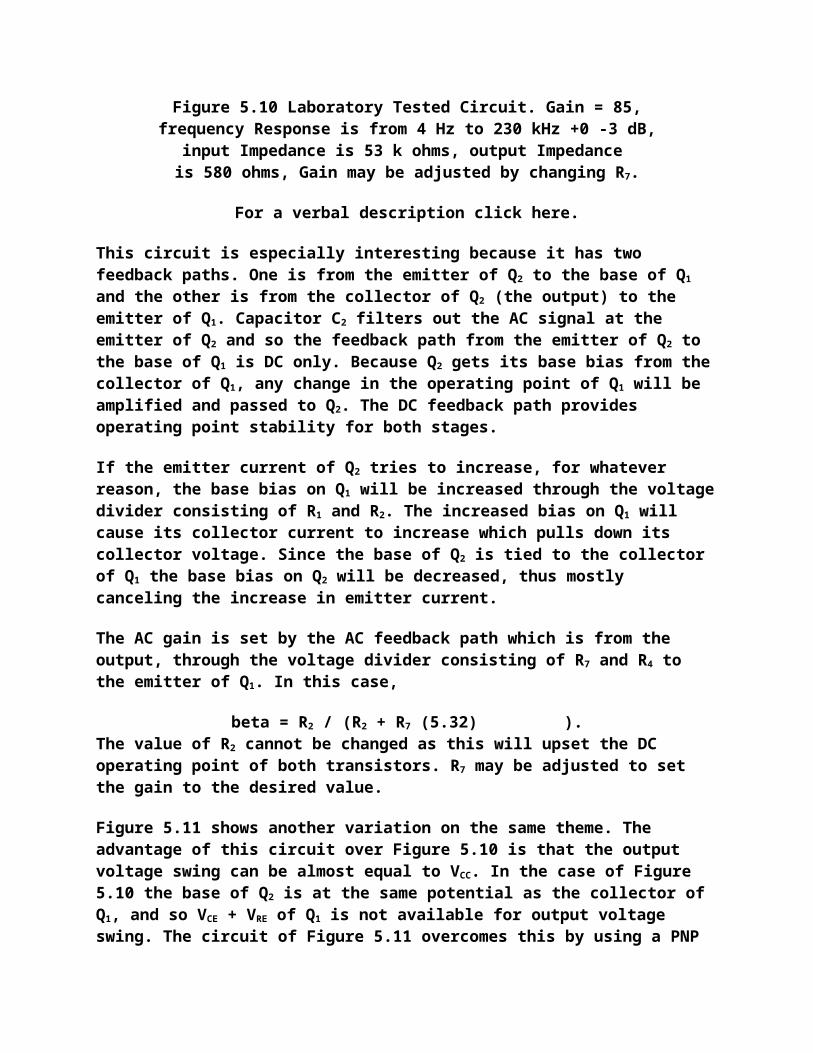
in the power supply voltage (no regulator is ever perfect) and other factors which seem to defy scientific explanation. Put a VFO in an environmental chamber, let it warm up for weeks or even months, operate it from an ultra precision power supply and it will never stop drifting.
Until the age of modern electronics the choice had to be either a fixed frequency and stable crystal oscillator or an adjustable frequency and drifting VFO. A circuit known as the frequency synthesizer is capable of combining the frequency agility of a VFO with the stability of a quartz crystal.
First of all a frequency synthesizer is not a musical instrument. A music synthesizer is comprised of an entirely different set of circuits. A frequency synthesizer can produce the musical scale but it can also produce any frequency in between the notes. The basic block diagram of a frequency synthesizer is shown in Figure 9.2.
Figure 9.2 Basic Block Diagram of a Frequency Synthesizer.
For a verbal description click here.
The circuit as drawn may also go by the name phase- locked loop. The V.C.O. is a voltage controlled oscillator. If the input voltage goes positive, the frequency of the V.C.O. will go up; if the input voltage goes negative the frequency will decrease. The phase detector has changed in recent years. It is now a digital circuit which can detect large frequency differences as well as small phase differences. If the frequency of input 2 is higher than the frequency of input 1, the output voltage of the detector goes negative. If the frequency of input 2 is lower than the frequency of input 1, the output voltage goes positive.
If the frequency of the V.C.O. is lower than it should be, the frequency of input 2 to the phase detector will be lower than the frequency of input 1 (the crystal oscillator) and the output voltage of the phase detector will go positive. This positive-going voltage will be
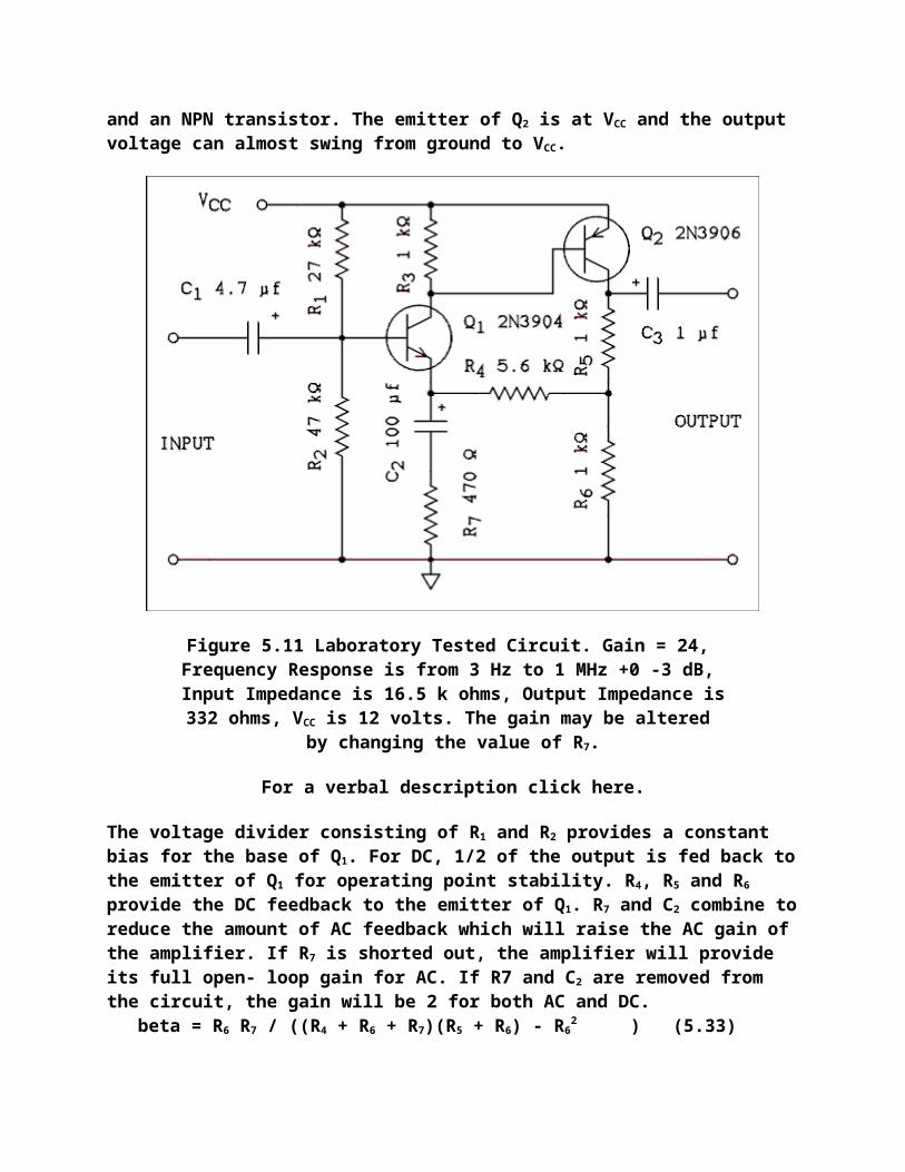
applied to the V.C.O., which will cause its frequency to increase. The circuit will soon find an equilibrium point at which the frequency at input 2 ( fVCO / N ) is equal to the frequency of the crystal oscillator. After the frequency is correct, the circuit goes to work on the phase angle. If the phase at input 2 is leading the phase at input 1, the output of the phase detector will go slightly negative and the phase error will be corrected to zero.
The unfiltered output of the phase detector is a series of positive or negative-going pulses whose width is proportional to the phase difference between the two input signals. If the phase angle could come to exactly zero the output of the phase detector would be an open circuit all of the time. (The output has a low impedance during the pulses but is an open circuit between pulses.) Nothing in this world is ever exact or perfect. There will always be some AC output from the phase detector. The RC network which is connected between the phase detector and the V.C.O. serves the purpose of filtering out most of the AC component of the output of the phase detector.
The filter requires two resistors in order to make the loop stable. An unstable loop will cause the frequency of the V.C.O. to jump around instead of locking on to the frequency of the crystal oscillator. Typical values for R1 and R2 are 1 M ohm and 100 k ohms, respectively. The value of the capacitor may range from 0.01 uf to 10 uf. If a given loop is unstable, R2 should be temporarily replaced by a resistor substitution box and the value "played with" until the loop is stable. The capacitor should be as large as possible consistent with the minimum lock-in time of the loop.
The frequencies at inputs 1 and 2 of the phase detector will always be equal. Therefore, if the frequency of the crystal oscillator is fR and the frequency of the V.C.O. is fO, then the frequency of the V.C.O. is given by
fO = N fR (9.1) The divide by N block is a variable modulus counter which is usually programmed by means of thumb-wheel switches. Because N is restricted to integer values, the smallest step in frequency which is possible is the frequency which is applied to input 1 of the phase detector. The smallest step is the resolution of the frequency synthesizer.
If a crystal cannot be obtained in a low enough frequency for the desired resolution the output of the oscillator may be divided by L as shown in Figure 9.3. The output frequency is now given by
fO = fR N / L (9.2) The resolution is now fR / L.
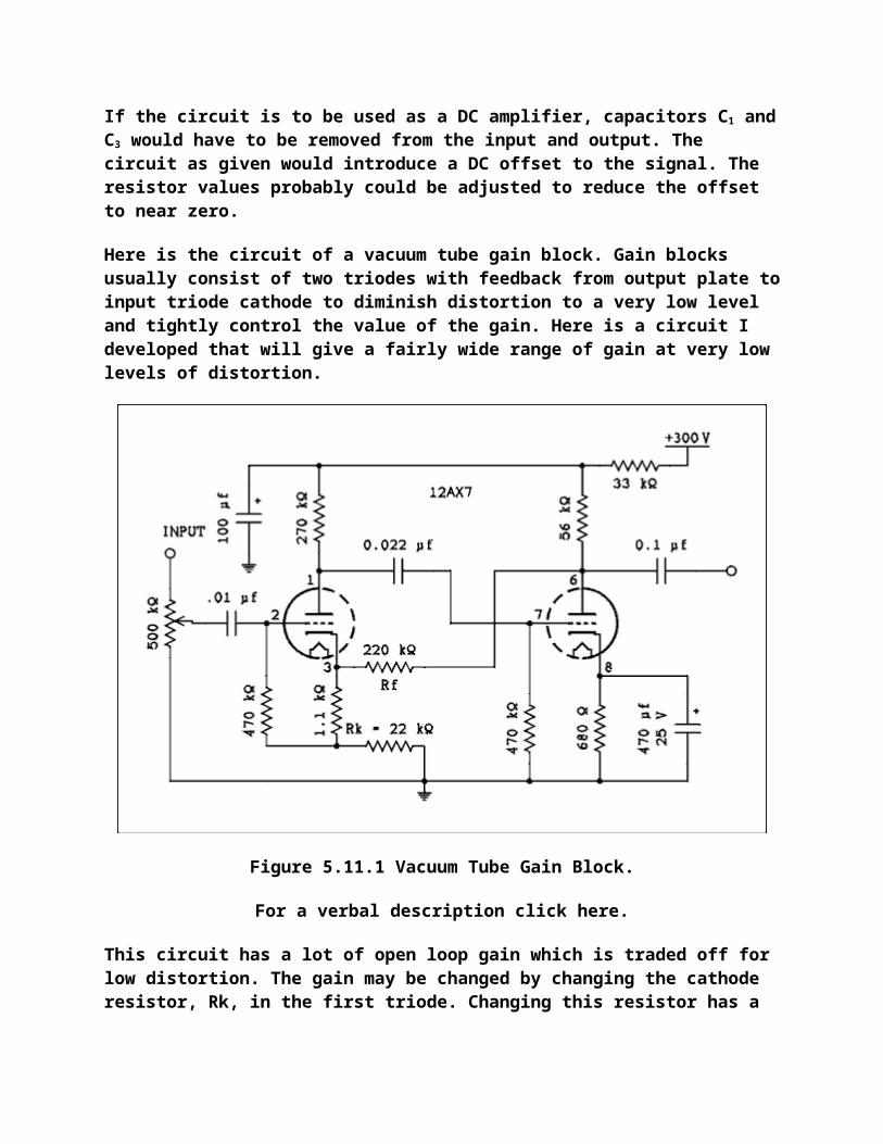
Figure 9.3 Frequency Synthesizer Circuit.
For a verbal description click here.
If the resolution is to be less than one hertz the input to the phase detector must also be less than 1 hertz. The required value of C in the loop filter is so large that it takes a very long time for the loop to lock in again after the value of N has been changed. Another way to get fractional hertz changes is to insert yet another divider in the circuit also shown in Figure 9.3. The divide by M circuit is a fixed modulus divider which divides the frequency of the V.C.O. before it is delivered to the output terminal. The output frequency is given by,
fO = fR N / (L M) (9.3) The resolution is fR / (L M).
Example 9.1.
In a synthesizer similar to Figure 9.3 the frequency of the crystal oscillator is 100 kHz, L = 5,000, M = 400 and 10 is less than N is less than 10,000. What are (a) the frequency range and resolution of the output and (b) the frequency range of the V.C.O.?
Solution:
The frequency at input 1 of the phase detector is 100 kHz / 5,000 = 20 Hz. The frequency at input 2 is also 20 Hz and so the frequency of the V.C.O. ranges from 10 x 20 Hz to 10,000 x 20 Hz = 200 Hz to 200 khz, which is the answer to part (b). The output frequency is the V.C.O. frequency divided by 400, which is 200 Hz / 400 to 200 kHz / 400 = 0.5 Hz to 500 hz, which is the first part of (a). The smallest frequency step for the V.C.O. is 20 Hz. The smallest step for the output is 20 Hz / 400 = 0.05 hz.
The output will go from 0.5 Hz to 500 Hz in 0.05 Hz steps. The V.C.O. must be capable of being tuned from 200 Hz to 200 kHz.
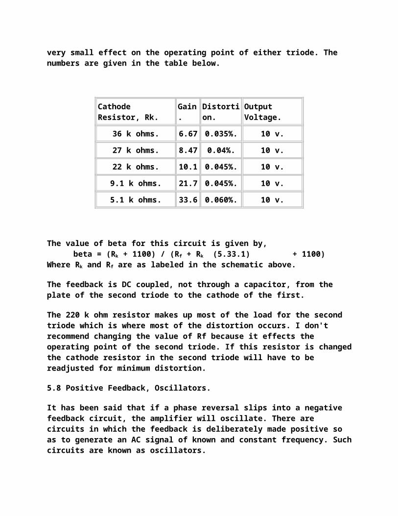
9.4 Problems.
1. A frequency counter has an 8 digit display and any one of the decimal points can be illuminated. If the gate time is 100 us and the readout is in MHz, where should the decimal point be placed. Number the digits from left to right and state which two the decimal point is between.
2. A DMM uses the 200 mV range to measure current. What resistor should be used as a shunt on the 20 mA range?
3. A DMM uses the 2 volt range for the 200 ohm range. What is the constant current for this range?
4. In a synthesizer similar to Figure 9.3 the frequency of the crystal oscillator is 2 MHz, L = 40,000, M = 5,000 and 45,000 is less than N is less than 75,000. What are (a) the frequency range of the V.C.O and (b) the frequency range and resolution of the output?
9.5 Answers to Problems.
1. Between 6 and 7. 2. 10 ohms. 3. 10 mA. 4. (a) 2.25 to 3.75 MHz. (b) 450 to 750 Hz in 0.01 Hz steps.
This page copyright © Max Robinson. All rights reserved.
Appendix A.Standard Values for Electronic Components.
Resistors, capacitors, some lines of RF chokes, and zener diodes come in standard values. The numbers may seem rather strange but they are based on a geometric series which will be explained later.
There are sets of values for tolerances of plus or minus 5%, 10% and 20%. The table below gives the standard values for the decade between 10 and 91. A value an any other decade can be obtained simply by multiplying a number from the table by the appropriate power of 10.
5% 10% 20%
10 10 10
11 NV NV
12 12 NV
13 NV NV
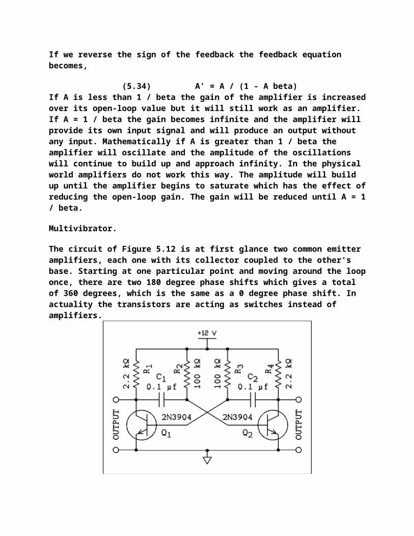
15 15 15
16 NV NV
18 18 NV
20 NV NV
22 22 22
24 NV NV
27 27 NV
30 NV NV
33 33 33
36 NV NV
39 39 NV
43 NV NV
47 47 47
51 NV NV
56 56 NV
62 NV NV
68 68 68
75 NV NV
82 82 NV
91 NV NV
Note, NV = No Value for this tolerance.
Why these strange values?
Let's take a 10 ohm 10% resistor as an example. That resistor could have any value between 9 and 11 ohms. It wouldn't make any sense to have an 11 ohm 10% resistor. That resistor could be anything between 9.9 and 12.1 ohms. The next higher 10% value is 12 ohms which may be anything between 10.8 and 13.2 ohms. True, there is a slight overlap but resistor values only have 2 significant digits and the next step up, 13 ohms would leave a substantial gap. The values are stepped so the tolerances just touch or overlap
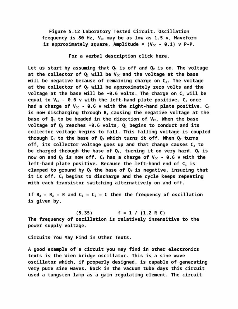
1/4 watt 5% resistors are manufactured in values from 1 ohm to 10 Meg ohms
This page copyright © Max Robinson. All rights reserved.
Appendix B.Reading Component Color and Numerical Codes.
Many beginners find resistor color codes to be confusing and capacitor codes to be completely unbreakable. This page should make it possible to understand how these codes work and remove the mystery from them.
Resistor color codes.
The basic code for 5 and 10 percent resistors uses three color bands plus a silver band indicating 10% or a gold band for 5%. You start reading on the end that the bands are closest to. Some 1/4 watt resistors have the bands equidistant from both ends. In that case
you have to rely on the gold or silver band to tell you where to start. You start on the end away from the gold or silver band. Here is a drawing of a typical resistor.
The first band may be double width indicating a wire wound resistor.
First of all each color stands for a digit as follows.
0 Black. 1 Brown. 2 Red. 3 Orange. 4 Yellow. 5 Green. 6 Blue. 7 Violet. 8 Gray. 9 White.
The first two bands on the left, A and B, form a two digit number. The third band, C, tells you how many zeros to place after that number. This is the number of ohms.
For example
Yellow, Violet, Black.
Start by writing down the digits 47. Then put zero zeros after it. The resistor is a 47 ohm.
Blue, Red Brown.
Write down 62 and put 1 zero after it giving 620 ohms.
Orange, White, Yellow.
39 with 4 zeros after it is 390,000 ohms.
For resistors less than 10 ohms the gold and silver colors appear in the third, C, band. A gold third band means A.B is the number of ohms. A silver third band means 0.AB ohms.
For example
Green, Blue, Gold.
This is a 5.6 ohm resistor.
Red, Violet, Silver.
This is a 0.27 ohm resistor.
If you have studied the section on scientific notation at the end of the Basic DC Circuits page the resistor color code is AB x 10C (A B times ten to the C). For this form gold is -1 and silver is -2.
Standard values.
Color coded resistors come only in certain values. If you want a 72 ohm resistor you can't get it because they are not made. The standard 5 and 10 percent values are as follows.
10 + 11 * 12 + 13 * 15 + 16 * 18 + 20 * 22 + 24 * 27 + 30 * 33 + 36 * 39 + 43 * 47 + 51 * 56 + 62 * 68 + 75 * 82 + 91 *
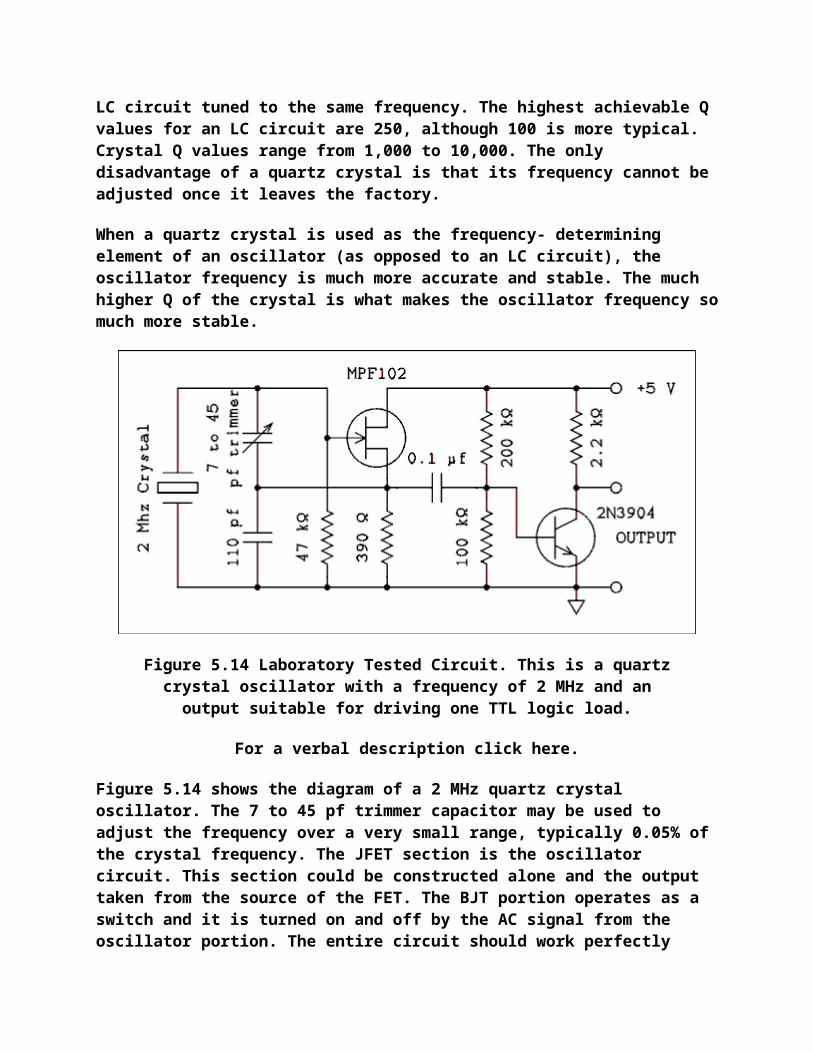
+ Available in 5 or 10 percent.* Available in 5 percent only.
The remaining decades repeat this one exactly. The list continues 100, 110, 120, 130, etc.
Why these funny numbers?
These values are set up so the tolerances just about touch or overlap slightly. For example a 10 ohm 5% may fall anywhere between 9.5 and 10.5 ohms. The 11 ohm 5% may fall anywhere from 10.45 to 11.55. There wouldn't be any point in making an 11 ohm 10% resistor. The 10 ohm 10% may be 9 to 11, the 11 ohm 10% may be 9.9 to 12.1 ohms, and the 12 ohm may be 10.8 to 13.2 ohms. If you put in a 10 ohm 10% you might actually get an 11 ohm. If you put in an 11 ohm 10% you might get 10, 9.9, 12, or 12.1 ohms. So by putting in an eleven ohm you might be getting the same results as a 10 ohm or 12 ohm. That's why you can't get an 11 ohm 10% resistor.
Four Band Codes.
Some 1 and 2 percent resistors use four bands to convey the value. The colors to numbers are the same but the code is ABC with D zeros after it. In scientific notation it is ABC x 10D (A B C times ten to the D). I confess I don't know how they handle values less then 100 ohms.
Numerical coding
Some resistors use a numerical code. It's the same as the color code except the code is given only in numbers. For example a resistor marked 503 is not a 5 hundred and 3 ohm resistor but the digits 5 0 followed by 3 zeros or 50,000 ohms. High wattage wire wound resistors are often marked in this way. Sometimes the number is followed by the letter k. Don't be fooled into thinking this means kilo ohms, it does not.
This code is also used on 1% or 0.1% resistors employing more digits. The last digit is the number of zeros that go after the first group of digits.
Antique Resistors.
Some antique resistors use the same code but the colors are arranged differently. One end of the resistor is one color, the body is another color and there is a color dot on the body. The body color is the first digit corresponding to band A on a modern resistor. The end color is the second digit, band B and the dot is the multiplier band C.
Capacitor Color Codes.
First of all, capacitors are coded in pico farads pronounced peko farads. Even a value that you are accustomed to thinking of in microfarads, such as a .1 microfarad is coded as 100,000 pico farads.
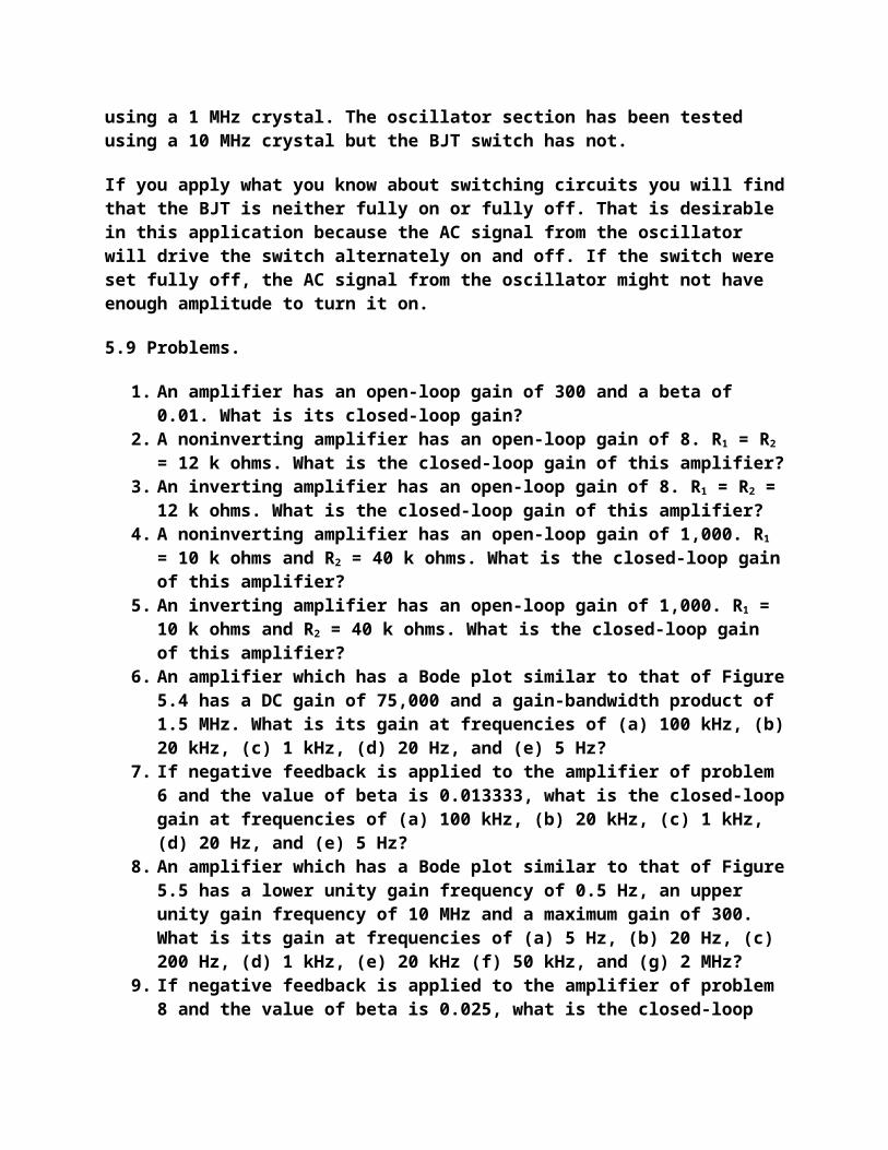
There are two types of flat capacitors and one cylindrical that use color codes. They are shown in the figure below.
The color codes read exactly the same as resistor color codes. If the capacitor has teardrop shaped dots hold it so the points are pointing to the right. If there is an arrow on the cap hold it so the arrow points right. If there is neither, look for writing on either side and hold it so the writing is right side up. If all of this fails try a digital capacitance meter.
The designations A, B, and C, have the same meanings as in the resistor color code. The number of pico farads is AB with C zeros after it. Or in scientific notation AB x 10<SUPC< sup> (A B times ten to the C).
The 6 dot capacitor.
The dots are numbered in a peculiar manner. The top row goes left to right but the bottom row goes right to left. Dot 1 is in the upper left and dot 6 is in the lower left. Go Figure.
Dot 1, upper left, tells you something about the capacitor. A black dot means the capacitor is mica. A silver dot means it is military specification paper. I have some caps on which this dot is white. I don't know what this means. Dots 2, 3, and 4, give the capacitance in pico farads as explained above. Dot 5 gives the percent tolerance as follows.
1% Brown. 2% Red. 3% Orange. 4% Yellow.
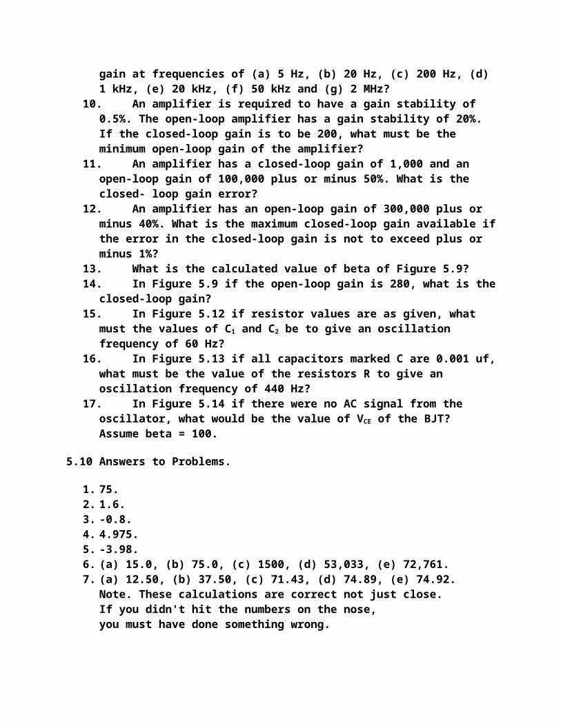
5% Green. 6% Blue. 7% Violet. 8% Gray. 9% White. 5% Gold. 10% Silver.
I have some caps on which this dot is black. Not a clue.
Dot 6 gives the temperature coefficient of capacitance in parts per million per degree Centigrade. The color coding is as follows.
Black -1000 to +1000. Brown -500 to +500. Red +200. Orange +100. Yellow -20 to +100. Green 0 to +70.
All of these capacitors have a voltage rating of 500 volts.
Three dot capacitors.
The three dot caps are read in a very straight forward manner; just as you would expect. They all have a 500 volt rating and plus or minus 20 percent tolerance.
Tubular Capacitors.
Cylindrical or tubular capacitors perhaps present the greatest enigma to the novice. The tubulars that have the leads coming out of each end as shown in the figure look like big resistors and I have known beginners to mistake them for resistors. These are military surplus paper capacitors.
The color code is read starting with the first band and is in pico farads. The fourth band gives the tolerance as follows.
Black + or - 20%. Brown + or - 1%. Red + or - 2%. Green + or - 5%. White + or - 10%.
Now things get a little ambiguous. I only have one of these caps in my possession and it is more than a little worse for wear. After the fourth band is an empty space. There may have been another band there which has been rubbed off. After that empty space, or missing band, is the voltage rating band. The voltages are given as follows.
Brown 100 V. Red 200 V. Orange 300 V. Yellow 400 V. Green 500 V. Blue 600 V. Violet 700 V. Gray 800 V. White 900 V. Gold 1000 V. Silver 2000 V. No color 500 V.
The one I have is a yellow, violet, yellow, black, blank, red which decodes to 470,000 pf 20% tolerance 200 volt.
The somewhat smaller ceramic types look as if the wire leads were wound around each end, as indeed they were, and come off the cap at right angles. These caps are often hollow and you can see right through them. The colors are not bands but small dots of paint that look as if they were painted on by hand. The first wide band may be a blob of paint which is larger than the rest.
I don't know what the first band means and can't find any reference to it in my extensive electronics literature. As indicated in the drawing above the second through fifth bands (spots) give the value and tolerance. For the tolerance use the table in this (tubular capacitors) section.
Many newer capacitor types use the numeric code. It works the same as the color code but numbers replace the color bands or dots. Often there is a letter such as J or K after the number. Don't be fooled into thinking the number is supposed to be multiplied by 1000. Not so. The meaning of these letters is known only to the manufacturer and a few privileged high volume buyers that the maker has informed. God likely doesn't know either as I doubt if any of these very rich men ever talk to Him.
This page copyright © Max Robinson. All rights reserved.
Appendix C.Transistor and IC Packages.
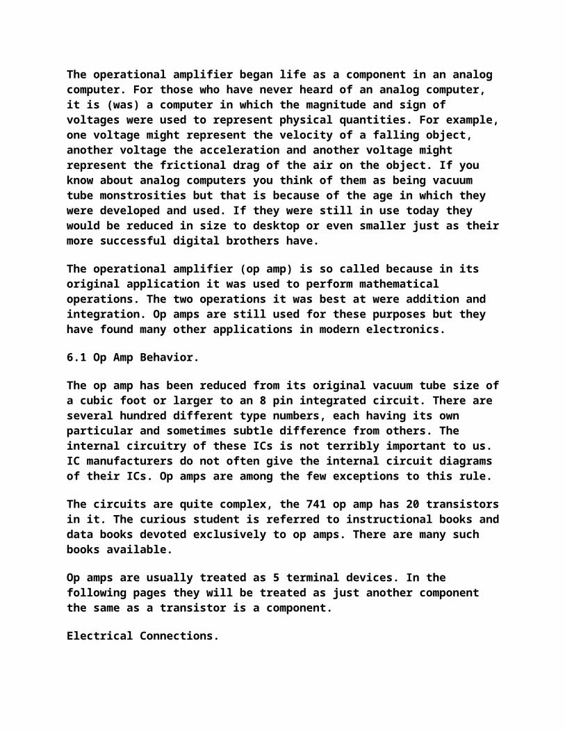
If one is going to do laboratory experiments or do it yourself construction projects, one must know how pins on various ICs and transistors are designated. There are literally hundreds of packages and one is not likely to run into most of them. Only the most commonly found packages are covered here.
On the left in the photo are an 8-pin and a 14-pin Dual Inline Package, DIP. The DIP comes in 6, 8, 14, 16, 18, 20, 24, 28, and 40-pin versions. The 24-pin and higher are twice the width of the smaller ones. Digital ICs, except for microprocessors, and analog devices, except for high input impedance amplifiers, come in DIPs. Military grade and wide temperature range industrial grade devices do not come in this plastic package.
Next is the TO-3 power package. Two are shown to reveal their appearance from top and bottom. Power transistors up to 200 watts and power ICs come in this style of package.
Next is the TO-5 package. Some of the best known early transistors, such as the 2N404 and 2N1302 came in this package. Premium quality ICs also come in the TO-5 configuration with 8, 10, or 12 pins, depending on the application.
Next is the ubiquitous TO-92 package. It is very inexpensive to manufacture and the low cost transistors in this package were, in part, responsible for the transistor boom of the 70s. 3-terminal voltage regulators are also sold in this package. They are limited to 3 pins.
Lastly is the almost as ubiquitous TO-220. Power transistors up to 50 watts and IC voltage regulators come in this package. It is sometimes seen with 4 or 5 pins.
The DIP.
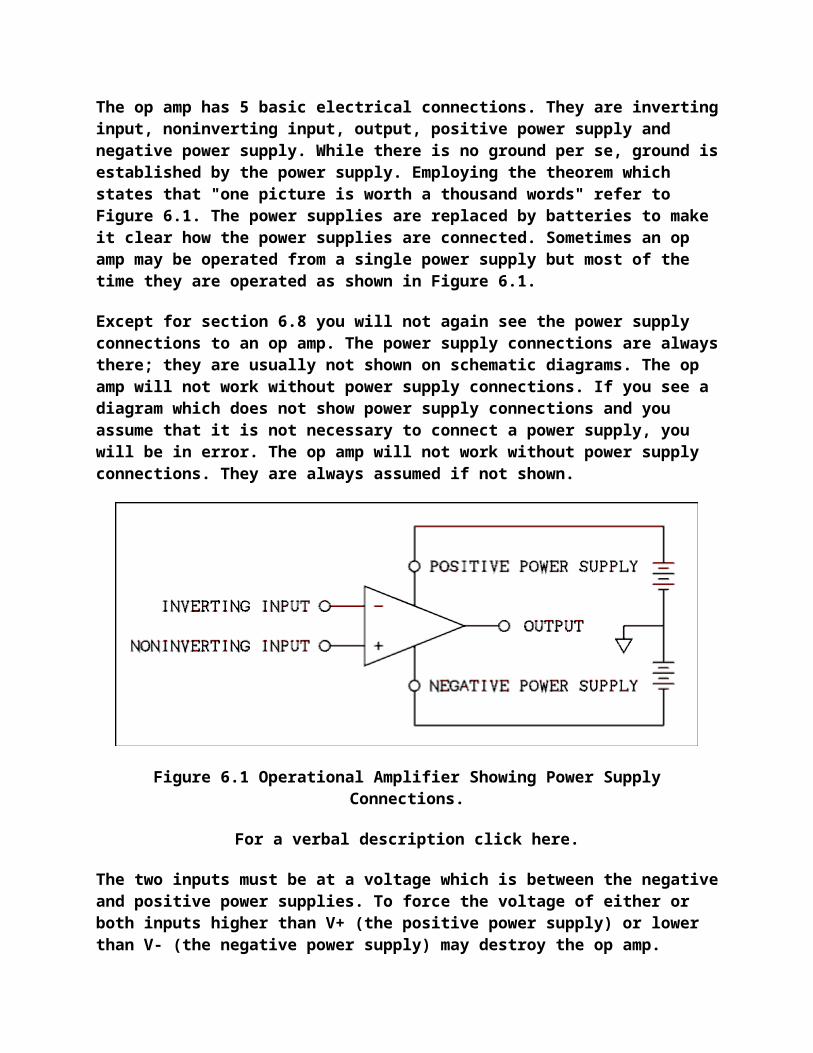
IC data books give pin numbers and the user of such circuits must know where to start and which way around to number the pins. The figure below shows the pin numbering convention for the DIP.
There are two types of packages. Part a shows the most common which has a small notch cut in the end between pins 1 and the highest numbered pin. The pins are counted counter clockwise as viewed from the TOP.
Part b shows a package used by Motorola. Pin 1 is marked with a dot and the pins are numbered counter clockwise as viewed from the TOP.
While the IC packages shown above are viewed from the top, these are viewed from the bottom. Some of the most common configurations will be given below but the student or experimenter should always consult the data sheet, or a data book for the particular transistor being used.
TO-3.
A drawing of the TO-3 package is not necessary. The photo clearly shows the letters E and B next to the pins. The metal case is the collector terminal.
In the case of an IC voltage regulator, the LM-309K to be specific, the pin on the right is the input and the left pin is the output. Backward? I think so but I didn't design it. The case is the common or ground. Always check the data sheet before wiring the circuit.
TO-5.
For most transistors in TO-5 packages the configuration is, 1 - Emitter,2 - Base,3 - Collector.
Always consult the data sheet for the particular transistor. The metal case may be connected to the base, the collector, or to none of the elements.
TO-92
For most bipolar transistors such as the 2N3904 and 2N3906 the pin configuration is, 1 - Emitter,2 - Base,3 - Collector.
For the very popular MPF102 field effect transistor the pin-out is, 1 - Drain,2 - Source,3 - Gate.
For the positive low power voltage regulators, such as the 78L12, the pinout is, 1 - Output,2 - Ground,3 - Input.
For the negative low power voltage regulators, such as the 79L12, the pinout is, 1 - Ground,2 - Input,3 - Output.
Always consult the data sheet for the particular transistor or IC you are using.
TO-220.
For a bipolar transistor the pinout is, 1 - Base,2 - Collector,3 - Emitter.
For a positive voltage regulator such as the 7812 the pinout is, 1 - Input,2 - Ground,3 - Output.
For a negative voltage regulator such as the 7912 the pinout is, 1 - Ground,2 - Input,3 - Output.
Always consult the data sheet for the particular transistor or IC you are using.
This page copyright © Max Robinson. All rights reserved.