video on-screen display v6 - xilinx° supports 1080p@60 in all supported device families (1) 1. ......
TRANSCRIPT

Video On-Screen Display v6.0
LogiCORE IP Product Guide
PG010 November 18, 2015

Video On‐Screen Display v6.0 www.xilinx.com 2PG010 November 18, 2015
Table of Contents
IP Facts
Chapter 1: Overview
Feature Summary. . . . . . . . . . . . . . . . . . . . . . . . . . . . . . . . . . . . . . . . . . . . . . . . . . . . . . . . . . . . . . . . . . 7
Applications . . . . . . . . . . . . . . . . . . . . . . . . . . . . . . . . . . . . . . . . . . . . . . . . . . . . . . . . . . . . . . . . . . . . . . 8
Unsupported Features. . . . . . . . . . . . . . . . . . . . . . . . . . . . . . . . . . . . . . . . . . . . . . . . . . . . . . . . . . . . . . 8
Licensing and Ordering Information . . . . . . . . . . . . . . . . . . . . . . . . . . . . . . . . . . . . . . . . . . . . . . . . . . . 8
Chapter 2: Product Specification
Standards . . . . . . . . . . . . . . . . . . . . . . . . . . . . . . . . . . . . . . . . . . . . . . . . . . . . . . . . . . . . . . . . . . . . . . . . 9
Performance. . . . . . . . . . . . . . . . . . . . . . . . . . . . . . . . . . . . . . . . . . . . . . . . . . . . . . . . . . . . . . . . . . . . . . 9
Resource Utilization. . . . . . . . . . . . . . . . . . . . . . . . . . . . . . . . . . . . . . . . . . . . . . . . . . . . . . . . . . . . . . . 11
Port Descriptions . . . . . . . . . . . . . . . . . . . . . . . . . . . . . . . . . . . . . . . . . . . . . . . . . . . . . . . . . . . . . . . . . 16
I/O Interface and Timing . . . . . . . . . . . . . . . . . . . . . . . . . . . . . . . . . . . . . . . . . . . . . . . . . . . . . . . . . . . 22
Register Space . . . . . . . . . . . . . . . . . . . . . . . . . . . . . . . . . . . . . . . . . . . . . . . . . . . . . . . . . . . . . . . . . . . 27
Chapter 3: Designing with the Core
General Design Guidelines . . . . . . . . . . . . . . . . . . . . . . . . . . . . . . . . . . . . . . . . . . . . . . . . . . . . . . . . . 39
Algorithm . . . . . . . . . . . . . . . . . . . . . . . . . . . . . . . . . . . . . . . . . . . . . . . . . . . . . . . . . . . . . . . . . . . . . . . 44
Clock, Enable, and Reset Considerations . . . . . . . . . . . . . . . . . . . . . . . . . . . . . . . . . . . . . . . . . . . . . . 46
System Considerations . . . . . . . . . . . . . . . . . . . . . . . . . . . . . . . . . . . . . . . . . . . . . . . . . . . . . . . . . . . . 48
Chapter 4: Customizing and Generating the Core
Vivado Integrated Design Environment (IDE) . . . . . . . . . . . . . . . . . . . . . . . . . . . . . . . . . . . . . . . . . . 49
Interface . . . . . . . . . . . . . . . . . . . . . . . . . . . . . . . . . . . . . . . . . . . . . . . . . . . . . . . . . . . . . . . . . . . . . . . . 49
Output Generation. . . . . . . . . . . . . . . . . . . . . . . . . . . . . . . . . . . . . . . . . . . . . . . . . . . . . . . . . . . . . . . . 55
Chapter 5: Constraining the Core
Required Constraints . . . . . . . . . . . . . . . . . . . . . . . . . . . . . . . . . . . . . . . . . . . . . . . . . . . . . . . . . . . . . . 56
Send Feedback
Video On‐Screen Display v6.0 www.xilinx.com 3PG010 November 18, 2015
Chapter 6: Simulation
Chapter 7: Synthesis and Implementation
Chapter 8: C Model Reference
Unpacking and Model Contents . . . . . . . . . . . . . . . . . . . . . . . . . . . . . . . . . . . . . . . . . . . . . . . . . . . . . 59
Installation . . . . . . . . . . . . . . . . . . . . . . . . . . . . . . . . . . . . . . . . . . . . . . . . . . . . . . . . . . . . . . . . . . . . . . 61
Software Requirements. . . . . . . . . . . . . . . . . . . . . . . . . . . . . . . . . . . . . . . . . . . . . . . . . . . . . . . . . . . . 61
Interface . . . . . . . . . . . . . . . . . . . . . . . . . . . . . . . . . . . . . . . . . . . . . . . . . . . . . . . . . . . . . . . . . . . . . . . . 61
Example Code. . . . . . . . . . . . . . . . . . . . . . . . . . . . . . . . . . . . . . . . . . . . . . . . . . . . . . . . . . . . . . . . . . . . 71
Chapter 9: Test Bench
Demonstration Test Bench . . . . . . . . . . . . . . . . . . . . . . . . . . . . . . . . . . . . . . . . . . . . . . . . . . . . . . . . . 92
Appendix A: Verification, Compliance, and Interoperability
Simulation . . . . . . . . . . . . . . . . . . . . . . . . . . . . . . . . . . . . . . . . . . . . . . . . . . . . . . . . . . . . . . . . . . . . . . 94
Hardware Testing. . . . . . . . . . . . . . . . . . . . . . . . . . . . . . . . . . . . . . . . . . . . . . . . . . . . . . . . . . . . . . . . . 94
Interoperability . . . . . . . . . . . . . . . . . . . . . . . . . . . . . . . . . . . . . . . . . . . . . . . . . . . . . . . . . . . . . . . . . . 95
Appendix B: Migrating and Upgrading
Migrating to the Vivado Design Suite. . . . . . . . . . . . . . . . . . . . . . . . . . . . . . . . . . . . . . . . . . . . . . . . . 96
Upgrading in Vivado Design Suite. . . . . . . . . . . . . . . . . . . . . . . . . . . . . . . . . . . . . . . . . . . . . . . . . . . . 96
Appendix C: Debugging
Finding Help on Xilinx.com . . . . . . . . . . . . . . . . . . . . . . . . . . . . . . . . . . . . . . . . . . . . . . . . . . . . . . . . . 98
Debug Tools . . . . . . . . . . . . . . . . . . . . . . . . . . . . . . . . . . . . . . . . . . . . . . . . . . . . . . . . . . . . . . . . . . . . . 99
Hardware Debug . . . . . . . . . . . . . . . . . . . . . . . . . . . . . . . . . . . . . . . . . . . . . . . . . . . . . . . . . . . . . . . . 101
Interface Debug . . . . . . . . . . . . . . . . . . . . . . . . . . . . . . . . . . . . . . . . . . . . . . . . . . . . . . . . . . . . . . . . . 101
Appendix D: Additional Resources
Xilinx Resources . . . . . . . . . . . . . . . . . . . . . . . . . . . . . . . . . . . . . . . . . . . . . . . . . . . . . . . . . . . . . . . . . 105
References . . . . . . . . . . . . . . . . . . . . . . . . . . . . . . . . . . . . . . . . . . . . . . . . . . . . . . . . . . . . . . . . . . . . . 105
Revision History . . . . . . . . . . . . . . . . . . . . . . . . . . . . . . . . . . . . . . . . . . . . . . . . . . . . . . . . . . . . . . . . . 106
Notice of Disclaimer. . . . . . . . . . . . . . . . . . . . . . . . . . . . . . . . . . . . . . . . . . . . . . . . . . . . . . . . . . . . . . 106
Send Feedback

Video On‐Screen Display v6.0 www.xilinx.com 4PG010 November 18, 2015 Product Specification
Introduction
The Xilinx LogiCORE™ IP Video On-Screen Display core provides a flexible video processing block for alpha blending and compositing as well as simple text and graphics generation. Support for up to eight layers using a combination of external video inputs (from frame buffer or streaming video cores via AXI4-Stream interfaces) and internal graphics controllers (including text generators) is provided. The core is programmable through a comprehensive register interface to set and control screen size, background color, layer position, and more using logic or a microprocessor. A comprehensive set of interrupt status bits is provided for processor monitoring.
Features
• Supports alpha-blending 8 video/graphics layers
• Provides programmable background color
• Provides programmable layer position, size and z-plane order
• Generates filled and outlined transparent boxes
• Generates text with 1-bit or 2-bit per pixel color depth
• Provides configurable internal text string memory
• Provides configurable internal font memory for 8x8 or 16x16 pixel f ixed distance fonts
• Provides scaling text by 1x, 2x, 4x or 8x
• Supports graphics color palette of 16 or 256 colors
IP Facts
LogiCORE IP Facts Table
Core Specifics
Supported Device Family(1)
UltraScale+™ Families,UltraScale™ Architecture, Zynq®-7000, 7 Series
Supported User Interfaces
AXI4-Lite, AXI4-Stream (2)
Resources See Table 2-3 through Table 2-6.
Provided with Core
Documentation Product Guide
Design Files Encrypted RTL
Example Design Not Provided
Test Bench Verilog (3)
Constraints File XDC
Simulation Models
Encrypted RTL, VHDL or Verilog Structural,C-Model (3)
Supported Software Drivers (4)
Standalone
Tested Design Flows (5)
Design Entry Tools
Vivado® Design Suite
Simulation For supported simulators, see the Xilinx DesignTools: Release Notes Guide.
Synthesis Tools Vivado Synthesis
Support
Provided by Xilinx, Inc.
1. For a complete listing of supported devices, see the Vivado IP Catalog.
2. Video protocol as defined in the Video IP: AXI Feature Adoption section of AXI Reference Guide [Ref 1].
3. HDL test bench and C-Model available on the product page on Xilinx.com at http://www.xilinx.com/products/ipcenter/EF-DI-OSD.htm
4. Standalone driver details can be found in the SDK directory (<install_directory>/doc/usenglish/xilinx_drivers.htm). Linux OS and driver support information is available from the Xilinx Wiki page.
5. For the supported versions of the tools, see the Xilinx Design Tools: Release Notes Guide.
Send Feedback

Video On‐Screen Display v6.0 www.xilinx.com 5PG010 November 18, 2015 Product Specification
• Optional AXI4-Lite control interface
• AXI4-Stream data interfaces
• Supports 2 or 3 color component channels
• Supports 8, 10, and 12-bits per color component input and output
• Supports video frame sizes up to 4096x4096 pixels
° Supports 1080p@60 in all supported device families (1)
1. Performance on low power devices may be lower.
Send Feedback
Video On‐Screen Display v6.0 www.xilinx.com 6PG010 November 18, 2015
Chapter 1
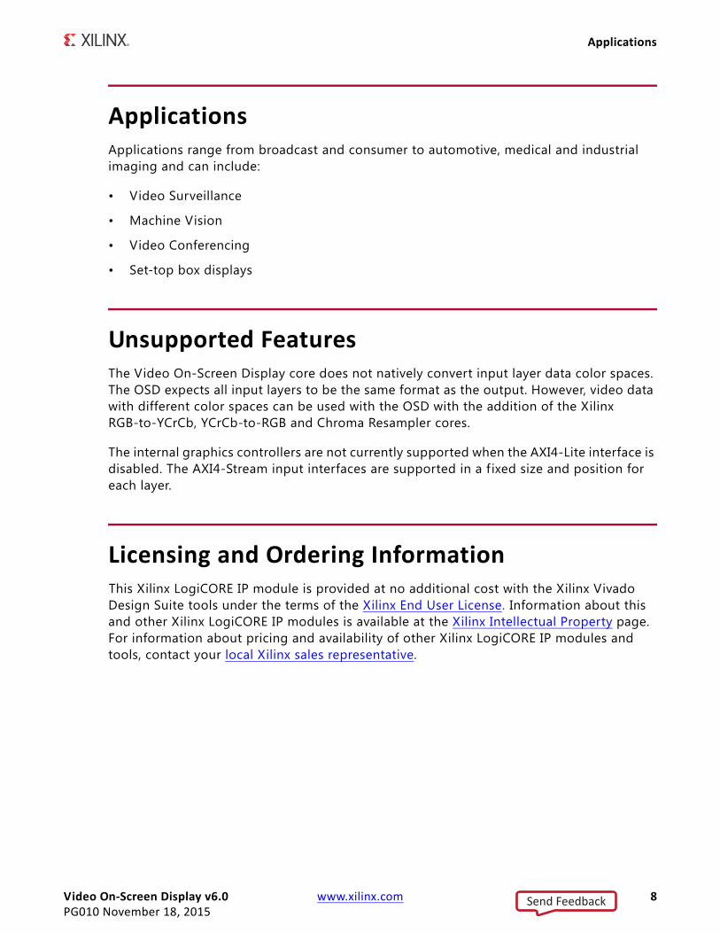
OverviewThe Xilinx LogiCORE ™ IP Video On-Screen Display (OSD) produces output video from multiple external video sources and multiple internal graphics controllers. Each graphics controller generates simple text and graphics overlays. Each video and graphics source is assigned an image layer. Up to eight image layers can be dynamically positioned, resized, brought forward or backward, and combined using alpha-blending.
Alpha-blending is the convex combination of two image layers allowing for transparency. Each layer in the OSD has a definite Z-plane order; or conceptually, each layer resides closer or farther from the observer having a different depth. Thus, the image and the image directly “over” it are blended. The order and amount of blending is programmable in real-time.
An example Xilinx Video On-Screen Display Output is shown in Figure 1-1.
Figure 1-1 shows an example OSD output with multiple video and graphics layers. The three video layers (Video 1, 2 and 3) can be still images or live video, and are combined with transparency to the programmable background color. Simple boxes and text are generated with one or multiple internal graphics controllers (shown with yellow text and menu buttons) and are blended with the other layers. Another video layer (the Xilinx logo), can be
X-Ref Target - Figure 1-1
Figure 1‐1: Example of OSD Output
Send Feedback

Video On‐Screen Display v6.0 www.xilinx.com 7PG010 November 18, 2015
Feature Summary
generated from on-chip or external memory, showing that the OSD output can be easily extended with external logic, a microprocessor, or memory storage.
Feature SummaryThe Video On-Screen Display core supports the AXI4-Lite and a constant interface mode. The AXI4-Lite interface allows the core to be easily integrated into an AXI microprocessor system with other AXI peripherals. The constant interface mode provides configuration options by the core Graphical User Interface (GUI). The user can use the GUI to configure a f ixed screen layout by setting the position and size of each AXI4-Stream input layer. (Graphics controllers are not currently supported in constant mode). These configurable interfaces allow the OSD to be easily integrated with AXI4 based processor systems, non-AXI4-compliant processor systems with little logic, and systems without a processor.
In addition, the OSD supports the AXI4-Stream Video Protocol on the input interfaces. These configurable input interfaces allow easy integration with other Xilinx Video IP cores including the AXI VDMA, Video Scaler, Color Space Converters, Chroma Resampler and Video Timing Controller. Other AXI4-Stream Video IP is also supported.
The Video On-Screen Display core is capable of operating at frequencies beyond those for 1080p60 or 1080p50 with 2 or 3 color components channels at 8, 10 or 12 bits per color component channel (equivalent supported bits per pixel: 16, 20, 24, 30 or 36 bits). This allows frame sizes up to 4096 x 4096 pixels to be displayed. The OSD also accepts up to eight input sources and performs alpha blending. The user can configure multiple input video sources from AXI4-Stream or external memory through the AXI VDMA. Each video source layer can be displayed at different cropped sizes, positions, and transparency to a programmable background color and other layers. In addition, each source layer can be displayed on top of or below other layers with a few register writes. Each layer can use pixel-level alpha values to enable non-rectangular masks and non-rectangular graphics overlays.
When using the Video On-Screen Display core, the eight video layers are not limited to external sources. The OSD also allows instantiating a set of internal graphics controllers. Each layer can be driven by a graphics controller, and each graphics controller can be configured independently. The graphics controllers contain box and text generators that can be reconfigured at runtime to move or resize text and boxes. Boxes can be filled or outlined and the outline width is configurable. Text is generated from an internal font that the user can load or reload at run time. Text can also be scaled up to eight times of the internal font with two or four colors for each string on the screen. The graphics controllers can be configured for 16 or 256 colors, and each color has an independent transparency alpha value. The runtime configurability of the graphics controller allows the user to generate dynamic animated displays that blend seamlessly with multiple video sources.
Send Feedback
Video On‐Screen Display v6.0 www.xilinx.com 8PG010 November 18, 2015
Applications
ApplicationsApplications range from broadcast and consumer to automotive, medical and industrial imaging and can include:
• Video Surveillance
• Machine Vision
• Video Conferencing
• Set-top box displays
Unsupported FeaturesThe Video On-Screen Display core does not natively convert input layer data color spaces. The OSD expects all input layers to be the same format as the output. However, video data with different color spaces can be used with the OSD with the addition of the Xilinx RGB-to-YCrCb, YCrCb-to-RGB and Chroma Resampler cores.
The internal graphics controllers are not currently supported when the AXI4-Lite interface is disabled. The AXI4-Stream input interfaces are supported in a f ixed size and position for each layer.
Licensing and Ordering InformationThis Xilinx LogiCORE IP module is provided at no additional cost with the Xilinx Vivado Design Suite tools under the terms of the Xilinx End User License. Information about this and other Xilinx LogiCORE IP modules is available at the Xilinx Intellectual Property page. For information about pricing and availability of other Xilinx LogiCORE IP modules and tools, contact your local Xilinx sales representative.
Send Feedback

Video On‐Screen Display v6.0 www.xilinx.com 9PG010 November 18, 2015
Chapter 2
Product Specification
StandardsThe Video On-Screen Display core is compliant with the AXI4-Stream Video Protocol and AXI4-Lite interconnect standards. Refer to the Video IP: AXI Feature Adoption section of the AXI Reference Guide [Ref 1] for additional information.
PerformanceThis section contains data about the typical performance of the Video On-Screen Display core.
Maximum Frequencies
This section contains typical clock frequencies for the target devices. The maximum achievable clock frequency can vary. The maximum achievable clock frequency and all resource counts can be affected by other tool options, additional logic in the device, using a different version of Xilinx tools, and other factors.
• Virtex-7, Kintex-7, Zynq (XC7Z030, XC7Z045): 225MHz
• Artix-7, Zynq (XC7Z010, XC7Z020): 150MHz
Latency
The Video On-Screen Display core can be configured for AXI4-Stream input interfaces. The latency to and from AXI4-Stream interfaces is a minimum of 16 + 4*C_NUM_LAYERS, but tready and tvalid will increase the overall latency of the core. The number of layers affects the latency. Each layer (configured by C_NUM_LAYERS) adds approximately four cycles.
Send Feedback

Video On‐Screen Display v6.0 www.xilinx.com 10PG010 November 18, 2015
Performance
Throughput
The Video On-Screen Display core throughput is mostly limited by the clock frequency and frame size (4096 x 4096 pixels). The other limiting factor is that the OSD also requires one extra line of initialization time each frame. This time is usually absorbed by the vertical blanking period in most video applications.
The typical maximum output throughput (AXI4-Stream output) is calculated by Equation 2-1.
Equation 2‐1
For AXI4-Stream output, this reduces to Equation 2-2:
Equation 2‐2
Table 2-1 shows the maximum achievable output throughput for the different target frequencies for AXI4-Stream interface.
In addition, the Video On-Screen Display core pads all input and output AXI4-Stream interfaces to the nearest byte. Table 2-2 shows the maximum achievable output throughput with the padding bits included.
Table 2‐1: AXI4‐Stream Throughput
ChannelsAlphaChannel
Channel Data Width
Bits per Pixel
Max ThroughputFMAX = 150 MHz
(Mbits/s)
Max Throughput FMAX = 225 MHz
(Mbits/s)
2 0 8 16 2399414206 3599121308
2 0 10 20 2999267757 4498901635
2 0 12 24 3599121308 5398681962
3 0 8 24 3599121308 5398681962
3 0 10 30 4498901635 6748352453
3 0 12 36 5398681962 8098022944
2 1 8 24 3599121308 5398681962
2 1 10 30 4498901635 6748352453
2 1 12 36 5398681962 8098022944
3 1 8 32 4798828411 7198242617
3 1 10 40 5998535514 8997803271
3 1 12 48 7198242617 10797363925
cycles per second lines per frame channels per pixel bits per channel cycles per frame
-------------------------------------------------------------------------------------------------------------------------------------------------------------
cycles per second 4096 channels per pixel bits per channel 4097
---------------------------------------------------------------------------------------------------------------------------------------
Send Feedback

Video On‐Screen Display v6.0 www.xilinx.com 11PG010 November 18, 2015
Resource Utilization
This can be compared to the user required throughput for any given video size by performing the calculation shown in Equation 2-3.
Equation 2‐3
Resource UtilizationResources required for devices are estimated in Table 2-3 through Table 2-6 and use the same configuration for estimating resources for Virtex-7 and Kintex-7 devices. UltraScale™ results are expected to be similar to 7 series results.
Resource usage values were generated using the Xilinx Vivado Design Suite. (Resource usage values generated using Vivado tools are expected to be similar.) They are derived from post-MAP reports, but may change due to optimization settings or post-PAR optimization.
All resource estimate configurations containing Graphics Controller layers have the Graphics Controller parameters set to the following:
• Instructions = 48
• Number of Colors = 16
• Number of Characters = 96
• Character Width = 8
Table 2‐2: AXI4‐Stream Throughput with Padding Bits
Channels Alpha Channel
Channel Data Width
Bits per Pixel
Max Throughput FMAX = 150 MHz
(bits/s)
Max Throughput FMAX = 225 MHz
(bits/s)
2 0 8 16 2399414206 3599121308
2 0 10 32 4798828411 7198242617
2 0 12 32 4798828411 7198242617
3 0 8 32 4798828411 7198242617
3 0 10 32 4798828411 7198242617
3 0 12 64 9597656822 14396485233
2 1 8 32 4798828411 7198242617
2 1 10 32 4798828411 7198242617
2 1 12 64 9597656822 14396485233
3 1 8 32 4798828411 7198242617
3 1 10 64 9597656822 14396485233
3 1 12 64 9597656822 14396485233
bitsondssec
------------------ framesondsec
---------------- linesframe------------- pixels
line------------- channels
pixel--------------------- bits
channel------------------=
Send Feedback

Video On‐Screen Display v6.0 www.xilinx.com 12PG010 November 18, 2015
Resource Utilization
• Character Height = 8
• ASCII Offset = 32
• Character Bits per Pixel = 1
• Number of Strings = 8
• Maximum String Length = 32
Different Graphics Controller parameter settings affect block RAM utilization. The following equation yields the upper bound of the block RAM utilization for Virtex-7 devices. The actual utilization may be lower due to block RAM data packing.
Number of Block RAMs <=
(Maximum Screen Width) * LOG2(Number of Colors) /8192
+ Instructions / 128
+ (Number of Characters) * (Character Width) * (Character Height) * (Character Bits per Pixel) / 8192
+ (Number of Strings) * (Maximum String Length) / 1024
The following equation yields the upper bound of the block RAM utilization for Kintex-7 devices. The actual utilization may be lower due to block RAM data packing.
Number of Block RAMs <=
(Maximum Screen Width) * LOG2(Number of Colors) /4096
+ Instructions / 128
+ (Number of Characters) * (Character Width) * (Character Height) * (Character Bits per Pixel) / 8192
+ (Number of Strings) * (Maximum String Length) / 1024
The Maximum Screen Width parameter does not affect the AXI4-Stream input layer resources.
Table 2-3 shows the resource estimates for Virtex-7 devices, and Table 2-4 shows the resource estimates for Kintex-7 devices.
Table 2‐3: Virtex‐7 FPGA Performance
Layer TypeData
Channel Width
Video Format
LayersMaximum Screen Width
XtremeDSP Slices
BRAM LUTs FFs
Graphics Controller 8 yuva_422 1 1280 2 2 2335 2500
Graphics Controller 8 yuva_422 2 1280 4 4 3804 3728
Send Feedback

Video On‐Screen Display v6.0 www.xilinx.com 13PG010 November 18, 2015
Resource Utilization
Graphics Controller 8 yuva_422 8 4095 16 24 11816 12344
Graphics Controller 8 yuva_444 1 1280 3 2 2338 2595
Graphics Controller 8 yuva_444 2 1280 6 4 3850 3898
Graphics Controller 8 yuva_444 8 4095 24 24 11746 13322
Graphics Controller 12 yuva_422 1 1280 2 2 2373 2723
Graphics Controller 12 yuva_422 2 1280 4 4 3893 4142
Graphics Controller 12 yuva_422 8 4095 16 24 12189 14162
Graphics Controller 12 yuva_444 1 1280 3 2 2384 2864
Graphics Controller 12 yuva_444 2 1280 6 4 3939 4419
Graphics Controller 12 yuva_444 8 4095 24 24 14107 16468
AXI4-Stream 8 yuva_422 1 1280 2 0 1245 1772
AXI4-Stream 8 yuva_422 2 1280 4 0 1536 2300
AXI4-Stream 8 yuva_422 8 4095 16 0 5119 7261
AXI4-Stream 8 yuva_444 1 1280 3 0 1256 1890
AXI4-Stream 8 yuva_444 2 1280 6 0 1565 2515
AXI4-Stream 8 yuva_444 8 4095 24 5560 8155
AXI4-Stream 12 yuva_422 1 1280 2 0 1261 1966
AXI4-Stream 12 yuva_422 2 1280 4 0 1639 2654
AXI4-Stream 12 yuva_422 8 4095 16 5865 8723
AXI4-Stream 12 yuva_444 1 1280 3 0 1282 2142
AXI4-Stream 12 yuva_444 2 1280 6 0 1694 3000
AXI4-Stream 12 yuva_444 8 4095 24 0 6991 11012
Table 2‐3: Virtex‐7 FPGA Performance (Cont’d)
Layer TypeData
Channel Width
Video Format
LayersMaximum Screen Width
XtremeDSP Slices
BRAM LUTs FFs
Table 2‐4: Kintex‐7 FPGA Performance
Layer TypeData
Channel Width
Video Format Layers
Maximum Screen Width
XtremeDSP Slices BRAM LUTs FFs
Graphics Controller 8 yuva_422 1 1280 2 2 2335 2500
Graphics Controller 8 yuva_422 2 1280 4 4 3803 3728
Graphics Controller 8 yuva_422 8 4095 16 24 11118 12134
Graphics Controller 8 yuva_444 1 1280 3 2 2341 2595
Graphics Controller 8 yuva_444 2 1280 6 4 3842 3898
Graphics Controller 8 yuva_444 8 4095 24 24 11635 13321
Graphics Controller 12 yuva_422 1 1280 2 2 2379 2723
Graphics Controller 12 yuva_422 2 1280 4 4 3889 4142
Send Feedback

Video On‐Screen Display v6.0 www.xilinx.com 14PG010 November 18, 2015
Resource Utilization
Graphics Controller 12 yuva_422 8 4095 16 24 13091 14701
Graphics Controller 12 yuva_444 1 1280 3 2 2377 2864
Graphics Controller 12 yuva_444 2 1280 6 4 3940 4419
Graphics Controller 12 yuva_444 8 4095 24 24 14103 16468
AXI4-Stream 8 yuva_422 1 1280 2 0 1244 1772
AXI4-Stream 8 yuva_422 2 1280 4 0 1529 2300
AXI4-Stream 8 yuva_422 8 4095 16 0 5129 7261
AXI4-Stream 8 yuva_444 1 1280 3 0 1252 1890
AXI4-Stream 8 yuva_444 2 1280 6 0 1568 2515
AXI4-Stream 8 yuva_444 8 4095 24 5516 8153
AXI4-Stream 12 yuva_422 1 1280 2 0 1261 1966
AXI4-Stream 12 yuva_422 2 1280 4 0 1637 2654
AXI4-Stream 12 yuva_422 8 4095 16 5827 8723
AXI4-Stream 12 yuva_444 1 1280 3 0 1285 2142
AXI4-Stream 12 yuva_444 2 1280 6 0 1692 3000
Table 2‐4: Kintex‐7 FPGA Performance (Cont’d)
Layer TypeData
Channel Width
Video Format
LayersMaximum Screen Width
XtremeDSP Slices
BRAM LUTs FFs
Table 2‐5: Artix‐7 FPGA Performance
Layer TypeData
Channel Width
Video Format LayersMaximum Screen Width
XtremeDSP Slices
BRAM LUTs FFs
Graphics Controller 8 yuva_422 1 1280 2 2 2334 2500
Graphics Controller 8 yuva_422 2 1280 4 4 3806 3728
Graphics Controller 8 yuva_422 8 4095 16 24 11004 12131
Graphics Controller 8 yuva_444 1 1280 3 2 2345 2595
Graphics Controller 8 yuva_444 2 1280 6 4 3845 3898
Graphics Controller 8 yuva_444 8 4095 24 24 12562 13511
Graphics Controller 12 yuva_422 1 1280 2 2 2361 2723
Graphics Controller 12 yuva_422 2 1280 4 4 3896 4142
Graphics Controller 12 yuva_422 8 4095 16 24 11987 14139
Graphics Controller 12 yuva_444 1 1280 3 2 2373 2864
Graphics Controller 12 yuva_444 2 1280 6 4 3938 4419
Graphics Controller 12 yuva_444 8 4095 24 24 12764 15835
AXI4-Stream 8 yuva_422 1 1280 2 0 1243 1772
AXI4-Stream 8 yuva_422 2 1280 4 0 1534 2300
AXI4-Stream 8 yuva_422 8 4095 16 0 5127 7261
Send Feedback
Video On‐Screen Display v6.0 www.xilinx.com 15PG010 November 18, 2015
Resource Utilization
AXI4-Stream 8 yuva_444 1 1280 3 0 1256 1890
AXI4-Stream 8 yuva_444 2 1280 6 0 1566 2515
AXI4-Stream 8 yuva_444 8 4095 24 0 5703 8456
AXI4-Stream 12 yuva_422 1 1280 2 0 1262 1966
AXI4-Stream 12 yuva_422 2 1280 4 0 1641 2654
AXI4-Stream 12 yuva_422 8 4095 16 0 6111 9122
AXI4-Stream 12 yuva_444 1 1280 3 0 1285 2142
AXI4-Stream 12 yuva_444 2 1280 6 0 1691 3000
Table 2‐5: Artix‐7 FPGA Performance (Cont’d)
Layer TypeData
Channel Width
Video Format LayersMaximum Screen Width
XtremeDSP Slices
BRAM LUTs FFs
Table 2‐6: Zynq ‐7000 Device Performance
Layer TypeData
Channel Width
Video Format
LayersMaximum Screen Width
XtremeDSP Slices
BRAM LUTs FFs
Graphics Controller 8 yuva_422 1 1280 2 2 2077 1800
Graphics Controller 8 yuva_422 2 1280 4 4 3374 2978
Graphics Controller 8 yuva_422 8 4095 16 24 11326 12066
Graphics Controller 8 yuva_444 1 1280 3 2 2159 1895
Graphics Controller 8 yuva_444 2 1280 6 4 3498 3164
Graphics Controller 8 yuva_444 8 4095 24 24 11823 13292
Graphics Controller 12 yuva_422 1 1280 2 2 2256 2007
Graphics Controller 12 yuva_422 2 1280 4 4 3643 3339
Graphics Controller 12 yuva_422 8 4095 16 24 12201 14119
Graphics Controller 12 yuva_444 1 1280 3 2 2329 2134
Graphics Controller 12 yuva_444 2 1280 6 4 3820 3588
Graphics Controller 12 yuva_444 8 4095 24 24 13064 15896
AXI4-Stream 8 yuva_422 1 1280 2 0 1041 1130
AXI4-Stream 8 yuva_422 2 1280 4 0 1430 1656
AXI4-Stream 8 yuva_422 8 4095 16 0 6343 7108
AXI4-Stream 8 yuva_444 1 1280 3 0 1094 1232
AXI4-Stream 8 yuva_444 2 1280 6 0 1511 1850
AXI4-Stream 12 yuva_422 1 1280 2 0 1164 1306
AXI4-Stream 12 yuva_422 2 1280 4 0 1613 1959
AXI4-Stream 12 yuva_444 2 1280 6 0 1725 2240
Send Feedback
Video On‐Screen Display v6.0 www.xilinx.com 16PG010 November 18, 2015
Port Descriptions
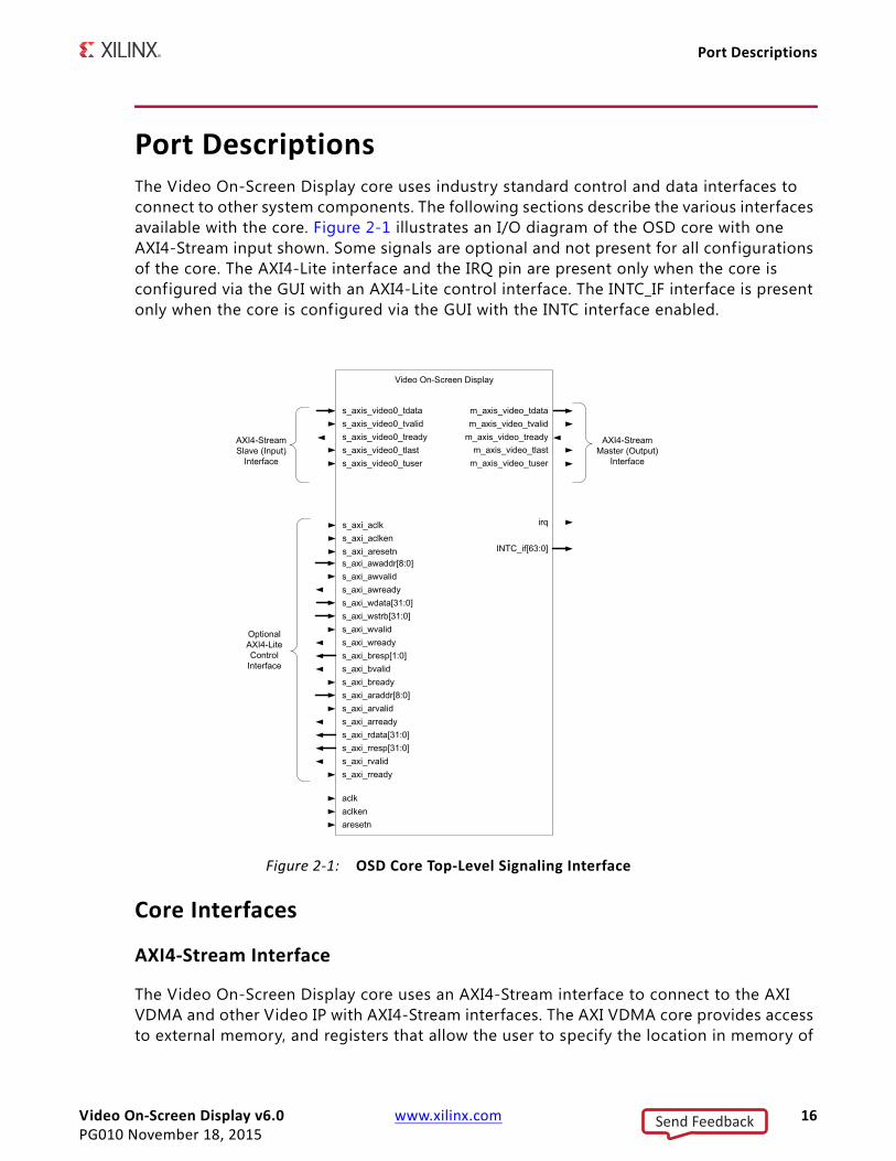
Port DescriptionsThe Video On-Screen Display core uses industry standard control and data interfaces to connect to other system components. The following sections describe the various interfaces available with the core. Figure 2-1 illustrates an I/O diagram of the OSD core with one AXI4-Stream input shown. Some signals are optional and not present for all configurations of the core. The AXI4-Lite interface and the IRQ pin are present only when the core is configured via the GUI with an AXI4-Lite control interface. The INTC_IF interface is present only when the core is configured via the GUI with the INTC interface enabled.
Core Interfaces
AXI4‐Stream Interface
The Video On-Screen Display core uses an AXI4-Stream interface to connect to the AXI VDMA and other Video IP with AXI4-Stream interfaces. The AXI VDMA core provides access to external memory, and registers that allow the user to specify the location in memory of
X-Ref Target - Figure 2-1
Figure 2‐1: OSD Core Top‐Level Signaling Interface
Video On-Screen Display
s_axis_video0_tdatas_axis_video0_tvalids_axis_video0_treadys_axis_video0_tlast
m_axis_video_tdatam_axis_video_tvalid
m_axis_video_treadym_axis_video_tlast
m_axis_video_tuser
AXI4-Stream Slave (Input)
Interface
OptionalAXI4-LiteControl
Interface
AXI4-Stream Master (Output)
Interfaces_axis_video0_tuser
aclkaclkenaresetn
s_axi_awaddr[8:0]s_axi_awvalids_axi_awreadys_axi_wdata[31:0]s_axi_wstrb[31:0]s_axi_wvalids_axi_wreadys_axi_bresp[1:0]s_axi_bvalids_axi_breadys_axi_araddr[8:0]s_axi_arvalids_axi_arreadys_axi_rdata[31:0]s_axi_rresp[31:0]s_axi_rvalids_axi_rready
INTC_if[63:0]
irqs_axi_aclks_axi_aclkens_axi_aresetn
Send Feedback

Video On‐Screen Display v6.0 www.xilinx.com 17PG010 November 18, 2015
Port Descriptions
the various layer data buffers that the OSD core accesses. The OSD core provides registers for configuring the placement, size and transparency of each video layer. The output is an AXI4-Stream interface.
Processor Interface
There are many video systems that use an integrated processor system to dynamically control the parameters within the system. This is important when several independent image processing cores are integrated into a single FPGA. The Video On-Screen Display core can be configured with an optional AXI4-Lite interface.
Common Interface Signals
Table 2-7 summarizes the signals which are NOT included in the AXI4 interfaces (AXI4-Lite and AXI4-Stream).
The ACLK, ACLKEN and ARESETn signals are shared between the core and the AXI4-Stream data interfaces. The AXI4-Lite control interface has its own set of clock, clock enable and reset pins: S_AXI_ACLK, S_AXI_ACLKEN and S_AXI_ARESETn. Refer to Interrupts for a detailed description of the INTC_IF and IRQ pins.
ACLK
The AXI4-Stream interface must be synchronous to the core clock signal ACLK. All AXI4-Stream interface input signals are sampled on the rising edge of ACLK. All AXI4-Stream output signal changes occur after the rising edge of ACLK. The AXI4-Lite interface is unaffected by the ACLK signal.
ACLKEN
The ACLKEN pin is an active-high, synchronous clock-enable input pertaining to AXI4-Stream interfaces. Setting ACLKEN low (de-asserted) halts the operation of the core
Table 2‐7: Common Interface Signals
Signal Name Direction Width Description
ACLK In 1 Video Core Clock
ACLKEN In 1 Video Core Active High Clock Enable
ARESETn In 1 Video Core Active Low Synchronous Reset
INTC_IFOut 6
INTERRUPT CONTROL INTERFACEOptional External Interrupt Controller Interface.Available only when "Include INTC_IF" is selected on GUI.
IRQOut 1
PROCESSOR INTERRUPTOptional Interrupt Request. Available only when "Include AXI4-Lite interface" is selected on GUI.
Send Feedback
Video On‐Screen Display v6.0 www.xilinx.com 18PG010 November 18, 2015
Port Descriptions
despite rising edges on the ACLK pin. Internal states are maintained, and output signal levels are held until ACLKEN is asserted again. When ACLKEN is de-asserted, core inputs are not sampled, except ARESETn, which supersedes ACLKEN. The AXI4-Lite interface is unaffected by the ACLKEN signal.
ARESETn
The ARESETn pin is an active-low, synchronous reset input pertaining to only AXI4-Stream interfaces. ARESETn supersedes ACLKEN, and when set to 0, the core resets at the next rising edge of ACLK even if ACLKEN is de-asserted. The ARESETn signal must be synchronous to the ACLK and must be held low for a minimum of 32 clock cycles of the slowest clock. The AXI4-Lite interface is unaffected by the ARESETn signal.
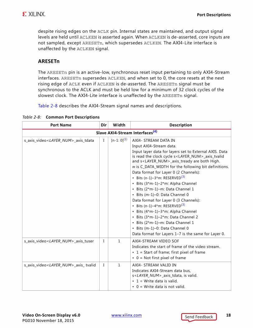
Table 2-8 describes the AXI4-Stream signal names and descriptions.
Table 2‐8: Common Port Descriptions
Port Name Dir Width Description
Slave AXI4‐Stream Interfaces(4)
s_axis_video<LAYER_NUM>_axis_tdata I [n-1: 0](1) AXI4- STREAM DATA INInput AXI4-Stream data. Input layer data for layers set to External AXIS. Data is read the clock cycle s<LAYER_NUM>_axis_tvalid and s<LAYER_NUM>_axis_tready are both High.m is C_DATA_WIDTH for the following bit definitions.Data format for Layer 0 (2 Channels):• Bits (n-1)–3*m: RESERVED(3)
• Bits (3*m-1)–2*m: Alpha Channel• Bits (2*m-1)–m: Data Channel 1• Bits (m-1)–0: Data Channel 0Data format for Layer 0 (3 Channels):• Bits (n-1)–4*m: RESERVED(3)
• Bits (4*m-1)–3*m: Alpha Channel• Bits (3*m-1)–2*m: Data Channel 2• Bits (2*m-1)–m: Data Channel 1• Bits (m-1)–0: Data Channel 0Data format for Layers 1–7 is the same for Layer 0.
s_axis_video<LAYER_NUM>_axis_tuser I 1 AXI4-STREAM VIDEO SOFIndicates the start of frame of the video stream.• 1 = Start of frame; f irst pixel of frame• 0 = Not first pixel of frame
s_axis_video<LAYER_NUM>_axis_ tvalid I 1 AXI4- STREAM VALID INIndicates AXI4-Stream data bus, s<LAYER_NUM>_axis_tdata, is valid.• 1 = Write data is valid.• 0 = Write data is not valid.
Send Feedback

Video On‐Screen Display v6.0 www.xilinx.com 19PG010 November 18, 2015
Port Descriptions
s_axis_video<LAYER_NUM>_axis_ tready O 1 AXI4- STREAM READYIndicates AXI4-Stream target is ready to receive stream data.• 1 = Ready to receive data.• 0 = Not ready to receive data.
s_axis_video<LAYER_NUM>_axis_ tlast I 1 AXI4-STREAM LASTIndicates last data beat per video line of AXI4-Stream data.• 1 = Last data beat of video line.• 0 = Not last data beat.
Master AXI4‐Stream Interface
m_axis_video_tdata O [n -1: 0] (2) AXI4- STREAM DATA OUTOutput AXI4-Stream data. Data format is the same as the s0_axis_tdata format except the m_axis_tdata bus has no alpha channel.
m_axis_video_tuser O 1 AXI4-STREAM VIDEO SOFIndicates the start of frame of the video stream.• 1 = Start of frame; f irst pixel of frame• 0 = Not first pixel of frame
m_axis_ video_tvalid O 1 AXI4- STREAM VALID OUTIndicates AXI4-Stream data bus, m_axis_tdata, is valid.• 1 = Write data is valid.• 0 = Write data is not valid.
m_axis_ video_tready I 1 AXI4- STREAM READYIndicates AXI4-Stream target is ready to receive stream data.• 1 = Ready to receive data.• 0 = Not ready to receive data.
m_axis_ video_tlast O 1 AXI4-STREAM LASTIndicates last data beat per video line of AXI4-Stream data.• 1 = Last data beat of video line.• 0 = Not last data beat.
1. The data width, n of the s<LAYER_NUM>_axis_tdata bus is calculated as the next multiple of 8 (padded to nearest byte) greater than the data channel width multiplied by the number of data channels including the alpha channel, or (C_NUM_DATA_CHANNELS+C_ALPHA_CHANNEL_EN)*C_DATA_WIDTH.
2. The data width, n, of the m_axis_tdata bus is calculated as the next multiple of 8 (padded to nearest byte) greater than the data channel width multiplied by the number of data channels excluding the alpha channel, or C_NUM_DATA_CHANNELS*C_DATA_WIDTH.
3. All reserved input pins must be driven by '0'.4. LAYER_NUM in the Slave AXI4-Stream interfaces indicates the layer number for that input. For example, if layer 3 is
configured for AXI4-Stream Input, then the ports for this input ares_axis_video3_tdata, s_axis_video3_tuser, s_axis_video3_tvalid, s_axis_video3_tready, and s_axis_video3_tlast.
Table 2‐8: Common Port Descriptions (Cont’d)
Port Name Dir Width Description
Send Feedback
Video On‐Screen Display v6.0 www.xilinx.com 20PG010 November 18, 2015
Port Descriptions
The ACLK, ACLKEN and ARESETn signals are shared between the core, the AXI4-Stream data interfaces, and the AXI4-Lite control interface.
Control Interface
When configuring the core, the user has the option to add an AXI4-Lite register interface to dynamically control the behavior of the core. The AXI4-Lite slave interface facilitates integrating the core into a processor system, or along with other video or AXI4-Lite compliant IP, connected via AXI4-Lite interface to an AXI4-Lite master. In a static configuration with a fixed set of parameters (constant configuration), the core can be instantiated without the AXI4-Lite control interface, which reduces the core Slice footprint.
Constant Configuration
The constant configuration enables users to instantiate the On-Screen Display core in a f ixed screen layout. The number of layers, their size, their position, their priority and alpha (if not using pixel-level alpha) is set at build time. Since there is no AXI4-Lite interface, the core is not programmable, but can be reset, enabled, or disabled using the ARESETn and ACLKEN ports. OSD graphics controllers are currently not supported by the constant configuration.
AXI4‐Lite Interface
The AXI4-Lite interface allows a user to dynamically control parameters within the core. Core configuration can be accomplished using an AXI4-Lite or AXI4-MM master state machine, or an embedded ARM or soft system processor such as MicroBlaze.
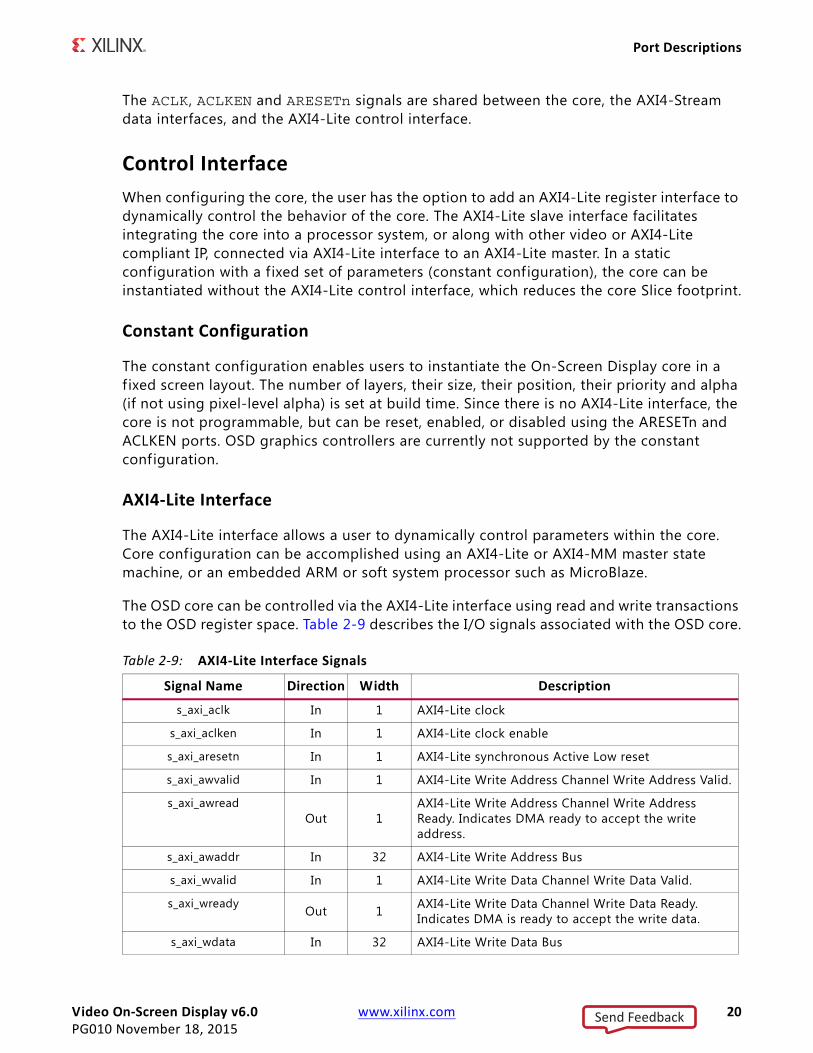
The OSD core can be controlled via the AXI4-Lite interface using read and write transactions to the OSD register space. Table 2-9 describes the I/O signals associated with the OSD core.
Table 2‐9: AXI4‐Lite Interface Signals
Signal Name Direction Width Description
s_axi_aclk In 1 AXI4-Lite clock
s_axi_aclken In 1 AXI4-Lite clock enable
s_axi_aresetn In 1 AXI4-Lite synchronous Active Low reset
s_axi_awvalid In 1 AXI4-Lite Write Address Channel Write Address Valid.
s_axi_awreadOut 1
AXI4-Lite Write Address Channel Write Address Ready. Indicates DMA ready to accept the write address.
s_axi_awaddr In 32 AXI4-Lite Write Address Bus
s_axi_wvalid In 1 AXI4-Lite Write Data Channel Write Data Valid.
s_axi_wready Out 1 AXI4-Lite Write Data Channel Write Data Ready. Indicates DMA is ready to accept the write data.
s_axi_wdata In 32 AXI4-Lite Write Data Bus
Send Feedback
Video On‐Screen Display v6.0 www.xilinx.com 21PG010 November 18, 2015
Port Descriptions
S_AXI_ACLK
The AXI4-Lite interface must be synchronous to the S_AXI_ACLK clock signal. The AXI4-Lite interface input signals are sampled on the rising edge of ACLK. The AXI4-Lite output signal changes occur after the rising edge of ACLK. The AXI4-Stream interfaces signals are not affected by the S_AXI_ACLK.
S_AXI_ACLKEN
The S_AXI_ACLKEN pin is an active-high, synchronous clock-enable input for the AXI4-Lite interface. Setting S_AXI_ACLKEN low (de-asserted) halts the operation of the AXI4-Lite interface despite rising edges on the S_AXI_ACLK pin. AXI4-Lite interface states are maintained, and AXI4-Lite interface output signal levels are held until S_AXI_ACLKEN is asserted again. When S_AXI_ACLKEN is de-asserted, AXI4-Lite interface inputs are not sampled, except S_AXI_ARESETn, which supersedes S_AXI_ACLKEN. The AXI4-Stream interfaces signals are not affected by the S_AXI_ACLKEN.
S_AXI_ARESETn
The S_AXI_ARESETn pin is an active-low, synchronous reset input for the AXI4-Lite interface. S_AXI_ARESETn supersedes S_AXI_ACLKEN, and when set to 0, the core resets at the next rising edge of S_AXI_ACLK even if S_AXI_ACLKEN is de-asserted. The S_AXI_ARESETn signal must be synchronous to the S_AXI_ACLK and must be held low for a minimum of 32 clock cycles of the slowest clock. The S_AXI_ARESETn input is
s_axi_bresp Out 2 AXI4-Lite Write Response Channel. Indicates results of the write transfer.
s_axi_bvalid Out 1 AXI4-Lite Write Response Channel Response Valid. Indicates response is valid.
s_axi_bready In 1 AXI4-Lite Write Response Channel Ready. Indicates target is ready to receive response.
s_axi_arvalid In 1 AXI4-Lite Read Address Channel Read Address Valid
s_axi_arready Out 1 Ready. Indicates DMA is ready to accept the read address.
s_axi_araddr In 32 AXI4-Lite Read Address Bus
s_axi_rvalid Out 1 AXI4-Lite Read Data Channel Read Data Valid
s_axi_rready In 1 AXI4-Lite Read Data Channel Read Data Ready. Indicates target is ready to accept the read data.
s_axi_rdata Out 32 AXI4-Lite Read Data Bus
s_axi_rresp Out 2 AXI4-Lite Read Response Channel Response. Indicates results of the read transfer.
Table 2‐9: AXI4‐Lite Interface Signals (Cont’d)
Signal Name Direction Width Description
Send Feedback

Video On‐Screen Display v6.0 www.xilinx.com 22PG010 November 18, 2015
I/O Interface and Timing
resynchronized to the ACLK clock domain. The AXI4-Stream interfaces and core signals are also reset by S_AXI_ARESETn.
I/O Interface and TimingThis section describes the signals and timing of the different interfaces of the Xilinx Video On-Screen Display.
Input AXI4‐Stream Slave Interface(s)
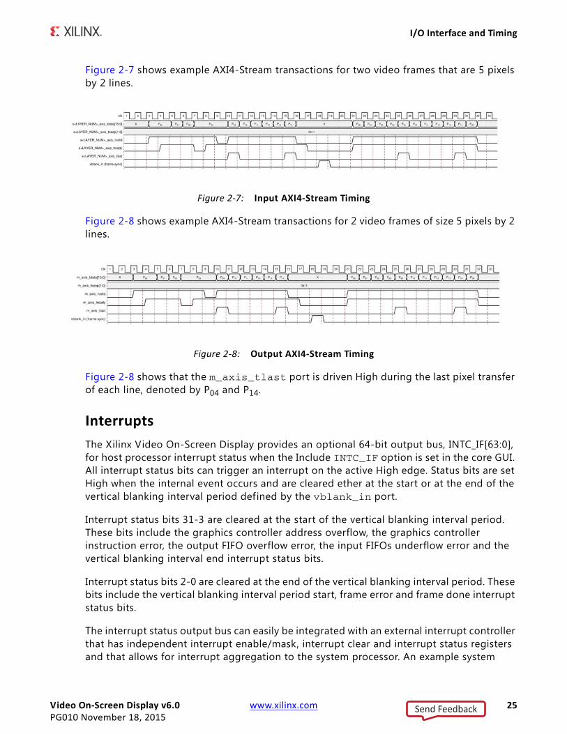
The Xilinx Video On-Screen Display can be configured to have up to eight input AXI4-stream slave interfaces. These interfaces include and require the TDATA, TVALID, TREADY and TLAST AXI4-Stream signals. The s<LAYER_NUM>_axis_tlast (TLAST) must be asserted High during the last TDATA transaction of each video line. The s<LAYER_NUM>_axis_tdata (TDATA) width must be a multiple of 8, with valid widths of 16, 24, 32, 40 or 48. Unused bits should be driven by zero. Figure 2-7 shows that the s<LAYER_NUM>_axis_tlast port is asserted High during the last pixel transfer of each line, denoted by P04 and P14s.
Video Data
The AXI4-Stream interface specif ication restricts TDATA widths to integer multiples of 8 bits. Therefore, 10 and 12 bit data must be padded with zeros on the MSB to form N*8 bit wide vector before connecting to s_axis_video_tdata. Padding does not affect the size of the core.
Similarly, data on the OSD output m_axis_video_tdata is packed and padded to multiples of 8 bits as necessary, as seen in the RGB/YCbCr examples shown in Figure 2-2, Figure 2-3, and Figure 2-4. Zero padding the most signif icant bits is only necessary for 10 and 12 bit wide data.
X-Ref Target - Figure 2-2
Figure 2‐2: 12‐bit RGB Data Encoding on TDATA
X-Ref Target - Figure 2-3
Figure 2‐3: 12‐bit YCbCr (4:4:4) Data Encoding on TDATA
Send Feedback

Video On‐Screen Display v6.0 www.xilinx.com 23PG010 November 18, 2015
I/O Interface and Timing
READY/VALID Handshake
A valid transfer occurs whenever READY, VALID, ACLKEN, and ARESETn are high at the rising edge of ACLK, as seen in Figure 2-5. During valid transfers, DATA only carries active video data. Blank periods and ancillary data packets are not transferred via the AXI4-Stream video protocol.
Guidelines on Driving s_axis_video_tvalid
Once s_axis_video_tvalid is asserted, no interface signals (except the OSD core driving s_axis_video_tready) may change value until the transaction completes (s_axis_video_tready, s_axis_video_tvalid, and ACLKEN are high on the rising edge of ACLK). Once asserted, s_axis_video_tvalid may only be de-asserted after a transaction has completed. Transactions may not be retracted or aborted. In any cycle following a transaction, s_axis_video_tvalid can either be de-asserted or remain asserted to initiate a new transfer.
Guidelines on Driving m_axis_video_tready
The m_axis_video_tready signal may be asserted before, during or after the cycle in which the OSD core asserted m_axis_video_tvalid. The assertion of m_axis_video_tready may be dependent on the value of m_axis_video_tvalid. A slave that can immediately accept data qualif ied by m_axis_video_tvalid, should pre-assert its m_axis_video_tready signal until data is received. Alternatively, m_axis_video_tready can be registered and driven the cycle following VALID
X-Ref Target - Figure 2-4
Figure 2‐4: 12‐bit YCbCr (4:2:2) Data Encoding on TDATA
X-Ref Target - Figure 2-5
Figure 2‐5: Example of READY/VALID Handshake, Start of a New Frame
Send Feedback

Video On‐Screen Display v6.0 www.xilinx.com 24PG010 November 18, 2015
I/O Interface and Timing
assertion. It is recommended that the AXI4-Stream slave should drive READY independently, or pre-assert READY to minimize latency.
Start of Frame Signals ‐ m_axis_video_tuser0, s_axis_video_tuser0
The Start-Of-Frame (SOF) signal, physically transmitted over the AXI4-Stream TUSER0 signal, marks the f irst pixel of a video frame. The SOF pulse is 1 valid transaction wide, and must coincide with the first pixel of the frame, as seen in Figure 2-5. SOF serves as a frame synchronization signal, which allows downstream cores to re-initialize, and detect the f irst pixel of a frame. The SOF signal may be asserted an arbitrary number of ACLK cycles before the first pixel value is presented on DATA , as long as a VALID is not asserted.
End of Line Signals ‐ m_axis_video_tlast, s_axis_video_tlast
The End-Of-Line signal, physically transmitted over the AXI4-Stream TLAST signal, marks the last pixel of a line. The EOL pulse is 1 valid transaction wide, and must coincide with the last pixel of a scan-line, as seen in Figure 2-6.
Output AXI4‐Stream Master Interface
The output interface of the Xilinx Video On-Screen Display can be configured to be a AXI4-Stream interface. This interface includes and requires the TDATA, TVALID, TREADY and TLAST AXI4-Stream signals. The m_axis_tlast (TLAST) will be driven High during the last TDATA transaction of each video line. The m_axis_tdata (TDATA) width must be a multiple of 8, with valid widths of 16, 24, 32 or 40. Unused bits will be driven by zero.
X-Ref Target - Figure 2-6
Figure 2‐6: Use of EOL and SOF Signals
Send Feedback
Video On‐Screen Display v6.0 www.xilinx.com 25PG010 November 18, 2015
I/O Interface and Timing
Figure 2-7 shows example AXI4-Stream transactions for two video frames that are 5 pixels by 2 lines.
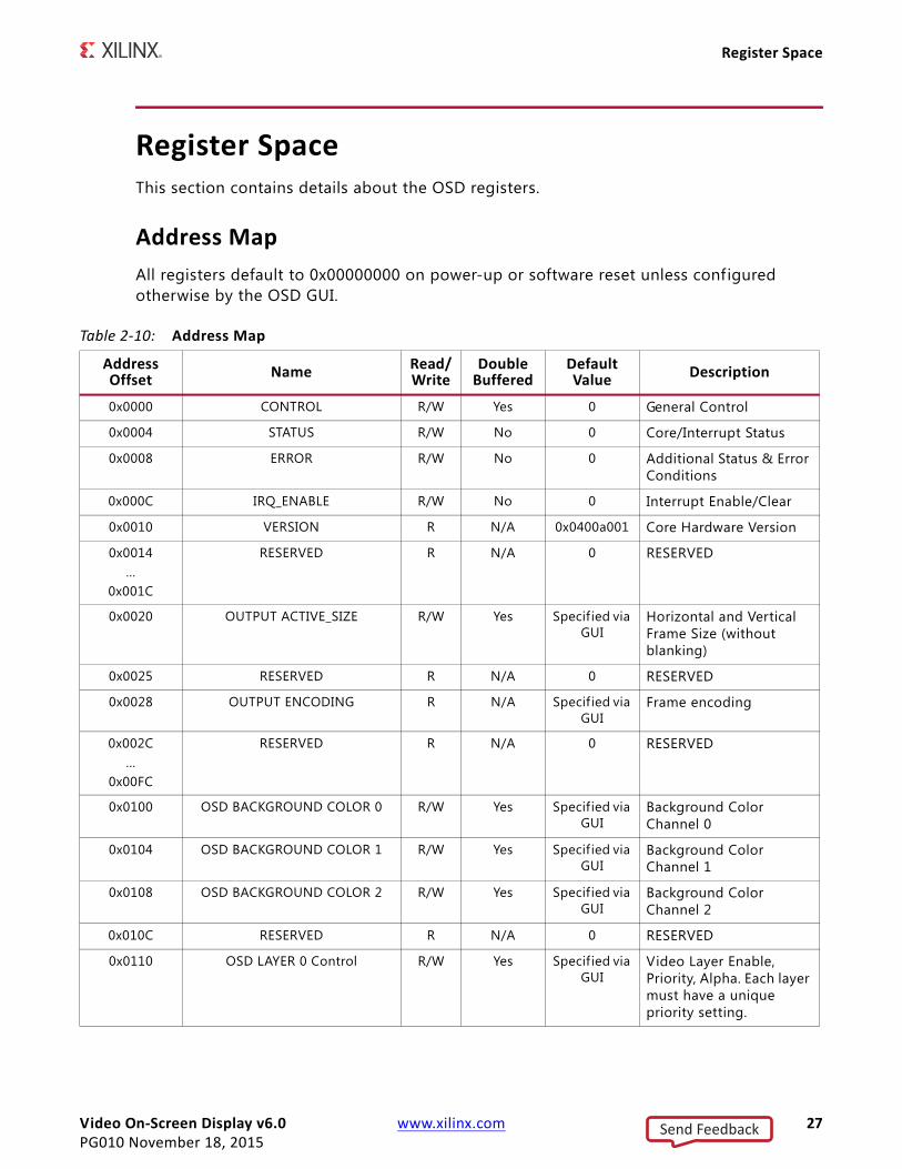
Figure 2-8 shows example AXI4-Stream transactions for 2 video frames of size 5 pixels by 2 lines.
Figure 2-8 shows that the m_axis_tlast port is driven High during the last pixel transfer of each line, denoted by P04 and P14.
Interrupts
The Xilinx Video On-Screen Display provides an optional 64-bit output bus, INTC_IF[63:0], for host processor interrupt status when the Include INTC_IF option is set in the core GUI. All interrupt status bits can trigger an interrupt on the active High edge. Status bits are set High when the internal event occurs and are cleared ether at the start or at the end of the vertical blanking interval period defined by the vblank_in port.
Interrupt status bits 31-3 are cleared at the start of the vertical blanking interval period. These bits include the graphics controller address overflow, the graphics controller instruction error, the output FIFO overflow error, the input FIFOs underflow error and the vertical blanking interval end interrupt status bits.
Interrupt status bits 2-0 are cleared at the end of the vertical blanking interval period. These bits include the vertical blanking interval period start, frame error and frame done interrupt status bits.
The interrupt status output bus can easily be integrated with an external interrupt controller that has independent interrupt enable/mask, interrupt clear and interrupt status registers and that allows for interrupt aggregation to the system processor. An example system
X-Ref Target - Figure 2-7
Figure 2‐7: Input AXI4‐Stream Timing
X-Ref Target - Figure 2-8
Figure 2‐8: Output AXI4‐Stream Timing
Send Feedback

Video On‐Screen Display v6.0 www.xilinx.com 26PG010 November 18, 2015
I/O Interface and Timing
showing the OSD and other processor peripherals connected to an interrupt controller is depicted in Figure 2-9.
The Xilinx Video On-Screen Display, when configured for the AXI4-Lite Interface, automatically contains an internal interrupt controller for enabling/masking and clearing each interrupt. The 1-bit output port, IRQ, is the interrupt output in this mode.
AXI4‐Lite Interface
The Xilinx Video On-Screen Display uses the AXI4-Lite Interface to interface to a microprocessor. Refer to the AMBA AXI4 Interface Protocol website (http://www.xilinx.com/ipcenter/axi4.htm) for more information on the AXI4 and AXI4-Lite interface signals.
X-Ref Target - Figure 2-9
Figure 2‐9: Interrupt Controller Processor Peripherals
Send Feedback
Video On‐Screen Display v6.0 www.xilinx.com 27PG010 November 18, 2015
Register Space
Register SpaceThis section contains details about the OSD registers.
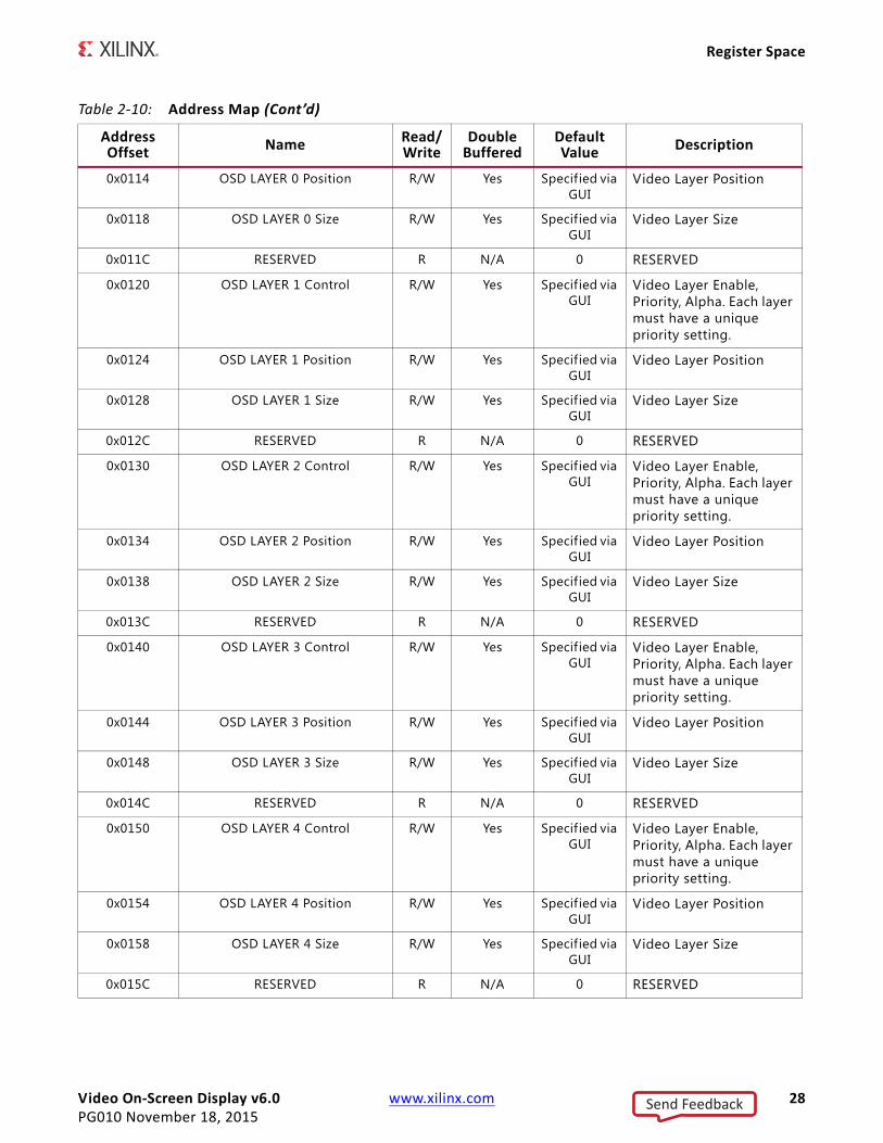
Address Map
All registers default to 0x00000000 on power-up or software reset unless configured otherwise by the OSD GUI.
Table 2‐10: Address Map
Address Offset Name
Read/Write
Double Buffered
Default Value Description
0x0000 CONTROL R/W Yes 0 General Control
0x0004 STATUS R/W No 0 Core/Interrupt Status
0x0008 ERROR R/W No 0 Additional Status & Error Conditions
0x000C IRQ_ENABLE R/W No 0 Interrupt Enable/Clear
0x0010 VERSION R N/A 0x0400a001 Core Hardware Version
0x0014…
0x001C
RESERVED R N/A 0 RESERVED
0x0020 OUTPUT ACTIVE_SIZE R/W Yes Specified via GUI
Horizontal and Vertical Frame Size (without blanking)
0x0025 RESERVED R N/A 0 RESERVED
0x0028 OUTPUT ENCODING R N/A Specified via GUI
Frame encoding
0x002C…
0x00FC
RESERVED R N/A 0 RESERVED
0x0100 OSD BACKGROUND COLOR 0 R/W Yes Specified via GUI
Background Color Channel 0
0x0104 OSD BACKGROUND COLOR 1 R/W Yes Specified via GUI
Background Color Channel 1
0x0108 OSD BACKGROUND COLOR 2 R/W Yes Specified via GUI
Background Color Channel 2
0x010C RESERVED R N/A 0 RESERVED
0x0110 OSD LAYER 0 Control R/W Yes Specified via GUI
Video Layer Enable, Priority, Alpha. Each layer must have a unique priority setting.
Send Feedback
Video On‐Screen Display v6.0 www.xilinx.com 28PG010 November 18, 2015
Register Space
0x0114 OSD LAYER 0 Position R/W Yes Specified via GUI
Video Layer Position
0x0118 OSD LAYER 0 Size R/W Yes Specified via GUI
Video Layer Size
0x011C RESERVED R N/A 0 RESERVED
0x0120 OSD LAYER 1 Control R/W Yes Specified via GUI
Video Layer Enable, Priority, Alpha. Each layer must have a unique priority setting.
0x0124 OSD LAYER 1 Position R/W Yes Specified via GUI
Video Layer Position
0x0128 OSD LAYER 1 Size R/W Yes Specified via GUI
Video Layer Size
0x012C RESERVED R N/A 0 RESERVED
0x0130 OSD LAYER 2 Control R/W Yes Specified via GUI
Video Layer Enable, Priority, Alpha. Each layer must have a unique priority setting.
0x0134 OSD LAYER 2 Position R/W Yes Specified via GUI
Video Layer Position
0x0138 OSD LAYER 2 Size R/W Yes Specified via GUI
Video Layer Size
0x013C RESERVED R N/A 0 RESERVED
0x0140 OSD LAYER 3 Control R/W Yes Specified via GUI
Video Layer Enable, Priority, Alpha. Each layer must have a unique priority setting.
0x0144 OSD LAYER 3 Position R/W Yes Specified via GUI
Video Layer Position
0x0148 OSD LAYER 3 Size R/W Yes Specified via GUI
Video Layer Size
0x014C RESERVED R N/A 0 RESERVED
0x0150 OSD LAYER 4 Control R/W Yes Specified via GUI
Video Layer Enable, Priority, Alpha. Each layer must have a unique priority setting.
0x0154 OSD LAYER 4 Position R/W Yes Specified via GUI
Video Layer Position
0x0158 OSD LAYER 4 Size R/W Yes Specified via GUI
Video Layer Size
0x015C RESERVED R N/A 0 RESERVED
Table 2‐10: Address Map (Cont’d)
Address Offset
Name Read/Write
Double Buffered
Default Value
Description
Send Feedback

Video On‐Screen Display v6.0 www.xilinx.com 29PG010 November 18, 2015
Register Space
0x0160 OSD LAYER 5 Control R/W Yes Specified via GUI
Video Layer Enable, Priority, Alpha. Each layer must have a unique priority setting.
0x0164 OSD LAYER 5 Position R/W Yes Specified via GUI
Video Layer Position
0x0168 OSD LAYER 5 Size R/W Yes Specified via GUI
Video Layer Size
0x016C RESERVED R N/A 0 RESERVED
0x0170 OSD LAYER 6 Control R/W Yes Specified via GUI
Video Layer Enable, Priority, Alpha. Each layer must have a unique priority setting.
0x0174 OSD LAYER 6 Position R/W Yes Specified via GUI
Video Layer Position
0x0178 OSD LAYER 6 Size R/W Yes Specified via GUI
Video Layer Size
0x017C RESERVED R N/A 0 RESERVED
0x0180 OSD LAYER 7 Control R/W Yes Specified via GUI
Video Layer Enable, Priority, Alpha. Each layer must have a unique priority setting.
0x0184 OSD LAYER 7 Position R/W Yes Specified via GUI
Video Layer Position
0x0188 OSD LAYER 7 Size R/W Yes Specified via GUI
Video Layer Size
0x018C RESERVED R N/A 0 RESERVED
0x0190 OSD GC Write Bank Address R/W No 0 Graphics Controller Write Bank Address. Used for all Instantiated Graphics Controllers
0x0194 OSD GC Active Bank Address R/W Yes 0 Graphics Controller Active Bank Addresses. Selected after next vblank. Used for all Instantiated Graphics Controllers
0x0198 OSD GC Data R/W No 0 Graphics Controller Data Register Used to write instructions, Character Map, ASCII text strings and color. Used for all Instantiated Graphics Controllers.
Table 2‐10: Address Map (Cont’d)
Address Offset
Name Read/Write
Double Buffered
Default Value
Description
Send Feedback
Video On‐Screen Display v6.0 www.xilinx.com 30PG010 November 18, 2015
Register Space
Note: All registers are little endian.
Note: Writing a '1' to a bit in the STATUS register clears the corresponding interrupt when set. Writing a '1' to a bit that is cleared, has no effect.
Table 2‐11: Control Register (Address Offset 0x0000)
0x0000 CONTROL R/W
Name B its Description
SW_RESET 31 Core reset. Writing a '1' will reset the core. This bit automatically clears when reset complete.
FSYNC_RESET 30 Frame Sync Core reset. Writing a '1' will reset the core after the start of the next input frame. This bit automatically clears when reset complete.
RESERVED 29:2 Reserved
REG_UPDATE 1 OSD Register Update Enable Setting this bit to 1 will cause the OSD to re-read all register values after the next start of frame. Setting this bit to 0 will cause the OSD to use its internally buffered register values. This Register update enable is not used for Graphics Controller Registers.
SW_ENABLE 0 Enable/Start the OSD This will cause the OSD to start reading from external memory and writing output
Table 2‐12: Stats Register (Address Offset 0x0004)
0x0004 STATUS R/W
Name B its Description
RESERVED 31:24 Reserved
LAYER7_ERROR 23 Layer 7 Error. When high check Error Register (0x0008) bits [31:28] for error status.
LAYER6_ERROR 22 Layer 6 Error. When high check Error Register (0x0008) bits [27:24] for error status.
LAYER5_ERROR 21 Layer 5 Error. When high check Error Register (0x0008) bits [23:20] for error status.
LAYER4_ERROR 20 Layer 4 Error. When high check Error Register (0x0008) bits [19:16] for error status.
LAYER3_ERROR 19 Layer 3 Error. When high check Error Register (0x0008) bits [15:12] for error status.
LAYER2_ERROR 18 Layer 2 Error. When high check Error Register (0x0008) bits [11:8] for error status.
LAYER1_ERROR 17 Layer 1 Error. When high check Error Register (0x0008) bits [7:4] for error status.
LAYER0_ERROR 16 Layer 0 Error. When high check Error Register (0x0008) bits [3:0] for error status.
RESERVED 15:2 Reserved
EOF 1 End-of-Frame. 1: Processing has reached end of frame. Occurs at the end of every frame. 0: Not currently at EOF.
PROC_STARTED 0 Processing Started. 1: Processing of frame data has begun. 0: Not currently processing.
Send Feedback
Video On‐Screen Display v6.0 www.xilinx.com 31PG010 November 18, 2015
Register Space
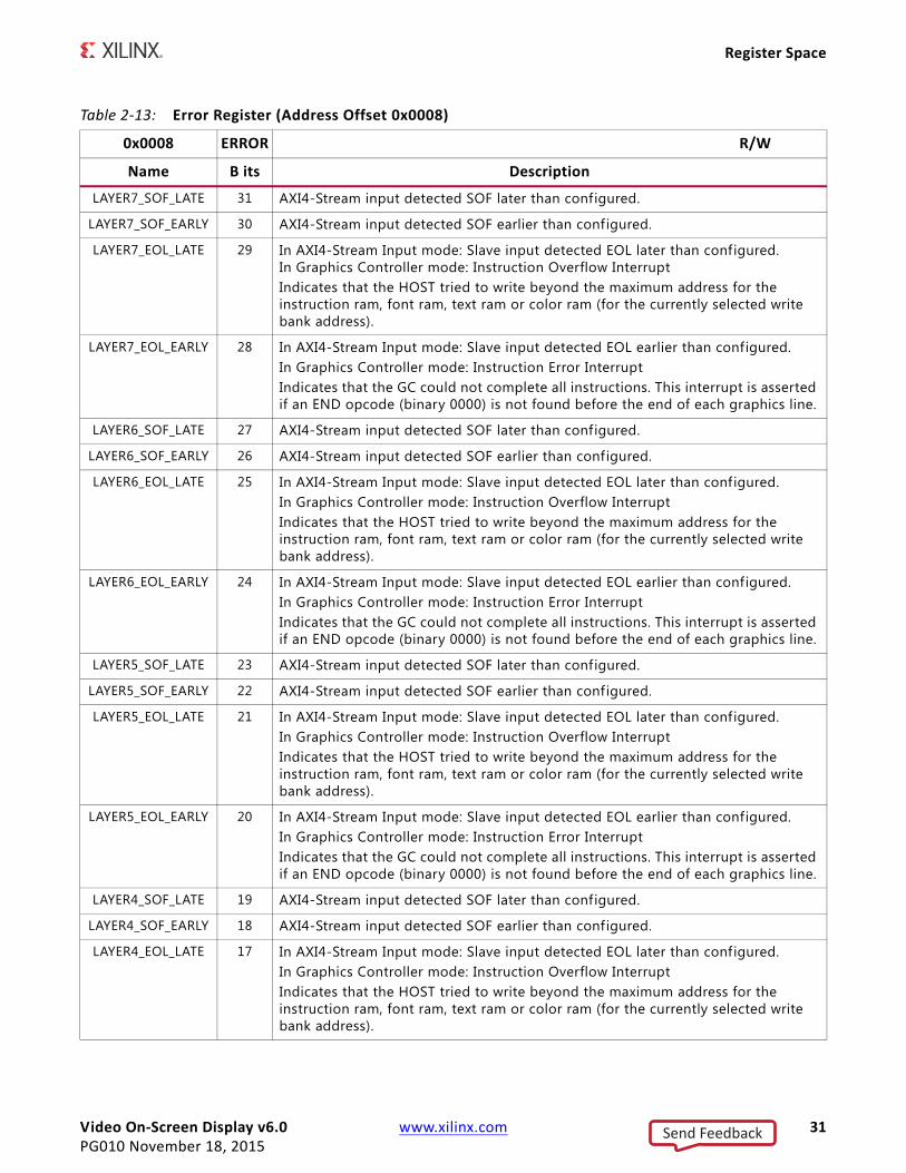
Table 2‐13: Error Register (Address Offset 0x0008)
0x0008 ERROR R/W
Name B its Description
LAYER7_SOF_LATE 31 AXI4-Stream input detected SOF later than configured.
LAYER7_SOF_EARLY 30 AXI4-Stream input detected SOF earlier than configured.
LAYER7_EOL_LATE 29 In AXI4-Stream Input mode: Slave input detected EOL later than configured. In Graphics Controller mode: Instruction Overflow Interrupt Indicates that the HOST tried to write beyond the maximum address for the instruction ram, font ram, text ram or color ram (for the currently selected write bank address).
LAYER7_EOL_EARLY 28 In AXI4-Stream Input mode: Slave input detected EOL earlier than configured. In Graphics Controller mode: Instruction Error Interrupt Indicates that the GC could not complete all instructions. This interrupt is asserted if an END opcode (binary 0000) is not found before the end of each graphics line.
LAYER6_SOF_LATE 27 AXI4-Stream input detected SOF later than configured.
LAYER6_SOF_EARLY 26 AXI4-Stream input detected SOF earlier than configured.
LAYER6_EOL_LATE 25 In AXI4-Stream Input mode: Slave input detected EOL later than configured. In Graphics Controller mode: Instruction Overflow Interrupt Indicates that the HOST tried to write beyond the maximum address for the instruction ram, font ram, text ram or color ram (for the currently selected write bank address).
LAYER6_EOL_EARLY 24 In AXI4-Stream Input mode: Slave input detected EOL earlier than configured. In Graphics Controller mode: Instruction Error Interrupt Indicates that the GC could not complete all instructions. This interrupt is asserted if an END opcode (binary 0000) is not found before the end of each graphics line.
LAYER5_SOF_LATE 23 AXI4-Stream input detected SOF later than configured.
LAYER5_SOF_EARLY 22 AXI4-Stream input detected SOF earlier than configured.
LAYER5_EOL_LATE 21 In AXI4-Stream Input mode: Slave input detected EOL later than configured. In Graphics Controller mode: Instruction Overflow Interrupt Indicates that the HOST tried to write beyond the maximum address for the instruction ram, font ram, text ram or color ram (for the currently selected write bank address).
LAYER5_EOL_EARLY 20 In AXI4-Stream Input mode: Slave input detected EOL earlier than configured. In Graphics Controller mode: Instruction Error Interrupt Indicates that the GC could not complete all instructions. This interrupt is asserted if an END opcode (binary 0000) is not found before the end of each graphics line.
LAYER4_SOF_LATE 19 AXI4-Stream input detected SOF later than configured.
LAYER4_SOF_EARLY 18 AXI4-Stream input detected SOF earlier than configured.
LAYER4_EOL_LATE 17 In AXI4-Stream Input mode: Slave input detected EOL later than configured. In Graphics Controller mode: Instruction Overflow Interrupt Indicates that the HOST tried to write beyond the maximum address for the instruction ram, font ram, text ram or color ram (for the currently selected write bank address).
Send Feedback

Video On‐Screen Display v6.0 www.xilinx.com 32PG010 November 18, 2015
Register Space
LAYER4_EOL_EARLY 16 In AXI4-Stream Input mode: Slave input detected EOL earlier than configured. In Graphics Controller mode: Instruction Error InterruptIndicates that the GC could not complete all instructions. This interrupt is asserted if an END opcode (binary 0000) is not found before the end of each graphics line.
LAYER3_SOF_LATE 15 AXI4-Stream input detected SOF later than configured.
LAYER3_SOF_EARLY 14 AXI4-Stream input detected SOF earlier than configured.
LAYER3_EOL_LATE 13 In AXI4-Stream Input mode: Slave input detected EOL later than configured. In Graphics Controller mode: Instruction Overflow Interrupt Indicates that the HOST tried to write beyond the maximum address for the instruction ram, font ram, text ram or color ram (for the currently selected write bank address).
LAYER3_EOL_EARLY 12 In AXI4-Stream Input mode: Slave input detected EOL earlier than configured. In Graphics Controller mode: Instruction Error InterruptIndicates that the GC could not complete all instructions. This interrupt is asserted if an END opcode (binary 0000) is not found before the end of each graphics line.
LAYER2_SOF_LATE 11 AXI4-Stream input detected SOF later than configured.
LAYER2_SOF_EARLY 10 AXI4-Stream input detected SOF earlier than configured.
LAYER2_EOL_LATE 9 In AXI4-Stream Input mode: Slave input detected EOL later than configured. In Graphics Controller mode: Instruction Overflow Interrupt Indicates that the HOST tried to write beyond the maximum address for the instruction ram, font ram, text ram or color ram (for the currently selected write bank address).
LAYER2_EOL_EARLY 8 In AXI4-Stream Input mode: Slave input detected EOL earlier than configured. In Graphics Controller mode: Instruction Error Interrupt Indicates that the GC could not complete all instructions. This interrupt is asserted if an END opcode (binary 0000) is not found before the end of each graphics line.
LAYER1_SOF_LATE 7 AXI4-Stream input detected SOF later than configured.
LAYER1_SOF_EARLY 6 AXI4-Stream input detected SOF earlier than configured.
LAYER1_EOL_LATE 5 In AXI4-Stream Input mode: Slave input detected EOL later than configured. In Graphics Controller mode: Instruction Overflow InterruptIndicates that the HOST tried to write beyond the maximum address for the instruction ram, font ram, text ram or color ram (for the currently selected write bank address).
LAYER1_EOL_EARLY 4 In AXI4-Stream Input mode: Slave input detected EOL earlier than configured. In Graphics Controller mode: Instruction Error Interrupt Indicates that the GC could not complete all instructions. This interrupt is asserted if an END opcode (binary 0000) is not found before the end of each graphics line.
LAYER0_SOF_LATE 3 AXI4-Stream input detected SOF later than configured.
LAYER0_SOF_EARLY 2 AXI4-Stream input detected SOF earlier than configured.
Table 2‐13: Error Register (Address Offset 0x0008) (Cont’d)
0x0008 ERROR R/W
Name B its Description
Send Feedback

Video On‐Screen Display v6.0 www.xilinx.com 33PG010 November 18, 2015
Register Space
Note: Writing a '1' to a bit in the ERROR register will clear the corresponding bit when set. If the bit is cleared and a '1' is written, this bit will be set.
Note: Setting a bit high in the IRQ_ENABLE register enables the corresponding interrupt. Bits that are low mask the corresponding interrupt from triggering.
LAYER0_EOL_LATE 1 In AXI4-Stream Input mode: Slave input detected EOL later than configured. In Graphics Controller mode: Instruction Overflow Interrupt Indicates that the HOST tried to write beyond the maximum address for the instruction ram, font ram, text ram or color ram (for the currently selected write bank address).
LAYER0_EOL_EARLY 0 In AXI4-Stream Input mode: Slave input detected EOL earlier than configured.In Graphics Controller mode: Instruction Error Interrupt Indicates that the GC could not complete all instructions. This interrupt is asserted if an END opcode (binary 0000) is not found before the end of each graphics line.
Table 2‐13: Error Register (Address Offset 0x0008) (Cont’d)
0x0008 ERROR R/W
Name B its Description
Table 2‐14: IRQ Enable Register (Address Offset 0x000C)
0x000C IRQ_ENABLE R/W
Name B its Description
RESERVED 31:24 Reserved
LAYER7_ERROR_EN 23 Layer 7 Error interrupt enable.
LAYER6_ERROR_EN 22 Layer 6 Error interrupt enable.
LAYER5_ERROR_EN 21 Layer 5 Error interrupt enable.
LAYER4_ERROR_EN 20 Layer 4 Error interrupt enable.
LAYER3_ERROR_EN 19 Layer 3 Error interrupt enable.
LAYER2_ERROR_EN 18 Layer 2 Error interrupt enable.
LAYER1_ERROR_EN 17 Layer 1 Error interrupt enable.
LAYER0_ERROR_EN 16 Layer 0 Error interrupt enable.
RESERVED 15:2 Reserved
EOF_EN 1 End-of-Frame interrupt enable.
PROC_STARTED_EN 0 Processing Started interrupt enable.
Table 2‐15: Version Register (Address Offset 0x0010)
0x0010 VERSION R
Name B its Description
MAJOR 31:24 Major version as a hexadecimal value (0x00 - 0xFF)
MINOR 23:16 Minor version as a hexadecimal value (0x00 - 0xFF)
Send Feedback

Video On‐Screen Display v6.0 www.xilinx.com 34PG010 November 18, 2015
Register Space
REVISION 15:12 Revision letter as a hexadecimal character from ('a' - 'f'). Mapping is as follows: 0XA->'a', 0xB->'b', 0xC->'c', 0xD->'d', etc.
PATCH_REVISION 11:8 Core Revision as a single 4-bit Hexadecimal value (0x0 - 0xF) Used for patch tracking.
INTERNAL_REVISION 7:0 Internal revision number. Hexadecimal value (0x00 - 0xFF)
Table 2‐16: Output Active Size Register (Address Offset 0x0020)
0x0020OUTPUT
ACTIVE_SIZER/W
Name B its Description
RESERVED 31:28 Reserved
ACTIVE_VSIZE 27:16 Vertical Active Frame Size. The height of the output frame without blanking in number of lines.
RESERVED 15:12 Reserved
ACTIVE_HSIZE 11:0 Horizontal Active Frame Size. The width of the output frame without blanking in number of pixels/clocks.
Table 2‐17: Output Encoding Register (Address Offset 0x0028)
0x0028OUTPUT
ENCODING R
Name B its Description
RESERVED 31:6 Reserved
NBITS 5:4 Number of bits per color component channel0: 8-bits 1: 10-bits 2: 12-bits 3: 16-bits (not currently supported)
VIDEO_FORMAT 3:0 Output Video Format 0: YUV 4:2:2 1: YUV 4:4:4 2: RGB 3: YUV 4:2:0
Table 2‐15: Version Register (Address Offset 0x0010) (Cont’d)
0x0010 VERSION R
Name B its Description
Send Feedback
Video On‐Screen Display v6.0 www.xilinx.com 35PG010 November 18, 2015
Register Space
Table 2‐18: OSD Background Color 0 Register (Address Offset 0x0100)
0x0100 OSD BACKGROUND COLOR 0 R/W
Name B its Description
RESERVED 31: C_S_AXIS_VIDEO_DATA_WIDTH Reserved
BACKGROUND COLOR 0
[C_S_AXIS_VIDEO_DATA_WIDTH-1:0] Background Color component of channel 0. Typically, Y (luma) or Green
Table 2‐19: OSD Background Color 1 Register (Address Offset 0x0104)
0x0104 OSD BACKGROUND COLOR 1 R/W
Name B its Description
RESERVED 31: C_S_AXIS_VIDEO_DATA_WIDTH Reserved
BACKGROUND COLOR 1 [C_S_AXIS_VIDEO_DATA_WIDTH-1:0] Background Color component of channel 1.Typically, U (Cb) or Blue
Table 2‐20: OSD Background Color 2 Register (Address Offset 0x0108)
0x0108 OSD BACKGROUND COLOR 2 R/W
Name B its Description
RESERVED 31: C_S_AXIS_VIDEO_DATA_WIDTH Reserved
BACKGROUND COLOR 2
[C_S_AXIS_VIDEO_DATA_WIDTH-1:0] Background Color component of channel 2. Typically, V (Cr) or Red
Table 2‐21: OSD Layer 0 Control Register (Address Offset 0x0110)
0x0110 OSD LAYER 0 CONTROL R/W
Name B its Description
RESERVED 31:17+ C_S_AXIS_VIDEO_DATA_WIDTH Reserved
LAYER0_ALPHA 16+ C_S_AXIS_VIDEO_DATA_WIDTH:16 Layer 0 Global Alpha Value Maximum Value (MAX):For Data Width of 8, MAX is 0x100.For Data Width of 10, MAX is 0x400.For Data Width of 12, MAX is 0x1000.0: 100% Transparent (Layer Off)...MAX: 0% Transparent (Blending Off)
RESERVED 15:11 Reserved
Send Feedback

Video On‐Screen Display v6.0 www.xilinx.com 36PG010 November 18, 2015
Register Space
Note: Setting the global alpha enable to 1 will override all alpha values for all colors in the graphics controller color table.
Note: 0x0110 - 0x0118 are repeated for Layers 1 through 7 at addresses 0x120 - 0x0188.
LAYER0_PRIORITY 10:8 Layer 0 Priority 0 = Lowest 1 = Higher ..7 = Highest
Note: Each layer must have a unique priority setting. Setting 2 or more layers to the same priority will have undesired effects on screen.
RESERVED 7:2 Reserved
LAYER0_GALPHA_EN 1 Layer 0 Global Alpha Enable
LAYER0_EN 0 Layer 0 Enable
Table 2‐21: OSD Layer 0 Control Register (Address Offset 0x0110) (Cont’d)
0x0110 OSD LAYER 0 CONTROL R/W
Name B its Description
Table 2‐22: OSD Layer 0 Position Register (Address Offset 0x0x114)
0x0x114 OSD Layer 0 Position R/W
Name Bits Description
Reserved 31:28 Reserved
Y position 27:16 Vertical start line of origin of layer. Origin of screen is located at (0,0).
Reserved 15:12
X position 11:0 Horizontal start pixel of origin of layer. Origin of screen is located at (0,0).
Table 2‐23: OSD Layer 0 Size Register (Address Offset 0x0118)
0x0118 OSD Layer 0 Size R/W
Name Bits Description
Reserved 31:28
Y size 27:16 Vertical Size of Layer
Reserved 15:12
X size 11:0 Horizontal Size of Layer
Send Feedback

Video On‐Screen Display v6.0 www.xilinx.com 37PG010 November 18, 2015
Register Space
Table 2‐24: OSD GC Write Bank Address Register (Address Offset 0x0190)
0x0190 OSD GC Write Bank Address R/W
Name Bits Description
Reserved 31:11
GC Number 10:8 Graphics Controller NumberThe Graphics Controller Layer Number. If a layer is configured for a graphics controller, then setting the layer number here will allow writing data to that graphics controller.
Reserved 7:3
GC_Write_Bank_ Addr
2:0 OSD GC Bank Write AddressControls which memory bank to write data.000: Write data into Instruction RAM 0001: Write data into Instruction RAM 1010: Write data into Color RAM 0011: Write data into Color RAM 1100: Write data into Text RAM 0101: Write data into Text RAM 1110: Write data into Font RAM 0111: Write data into Font RAM 1
Send Feedback
Video On‐Screen Display v6.0 www.xilinx.com 38PG010 November 18, 2015
Register Space
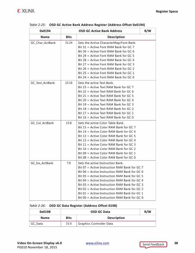
Table 2‐25: OSD GC Active Bank Address Register (Address Offset 0x0194)
0x0194 OSD GC Active Bank Address R/W
Name Bits Description
GC_Char_ActBank 31:24 Sets the Active CharacterMap/Font Bank.Bit 31 = Active Font RAM Bank for GC 7Bit 30 = Active Font RAM Bank for GC 6Bit 29 = Active Font RAM Bank for GC 5Bit 28 = Active Font RAM Bank for GC 4Bit 27 = Active Font RAM Bank for GC 3Bit 26 = Active Font RAM Bank for GC 2Bit 25 = Active Font RAM Bank for GC 1Bit 24 = Active Font RAM Bank for GC 0
GC_Text_ActBank 23:16 Sets the active Text Bank.Bit 23 = Active Text RAM Bank for GC 7Bit 22 = Active Text RAM Bank for GC 6Bit 21 = Active Text RAM Bank for GC 5Bit 20 = Active Text RAM Bank for GC 4Bit 19 = Active Text RAM Bank for GC 3Bit 18 = Active Text RAM Bank for GC 2Bit 17 = Active Text RAM Bank for GC 1Bit 16 = Active Text RAM Bank for GC 0
GC_Col_ActBank 15:8 Sets the active Color Table Bank.Bit 15 = Active Color RAM Bank for GC 7Bit 14 = Active Color RAM Bank for GC 6Bit 13 = Active Color RAM Bank for GC 5Bit 12 = Active Color RAM Bank for GC 4Bit 11 = Active Color RAM Bank for GC 3Bit 10 = Active Color RAM Bank for GC 2Bit 09 = Active Color RAM Bank for GC 1Bit 08 = Active Color RAM Bank for GC 0
GC_Ins_ActBank 7:0 Sets the active Instruction Bank.Bit 07 = Active Instruction RAM Bank for GC 7Bit 06 = Active Instruction RAM Bank for GC 6Bit 05 = Active Instruction RAM Bank for GC 5Bit 04 = Active Instruction RAM Bank for GC 4Bit 03 = Active Instruction RAM Bank for GC 3Bit 02 = Active Instruction RAM Bank for GC 2Bit 01 = Active Instruction RAM Bank for GC 1Bit 00 = Active Instruction RAM Bank for GC 0
Table 2‐26: OSD GC Data Register (Address Offset 0198)
0x0198 OSD GC Data R/W
Name Bits Description
GC_Data 31:0 Graphics Controller Data
Send Feedback
Video On‐Screen Display v6.0 www.xilinx.com 39PG010 November 18, 2015
Chapter 3
Designing with the CoreThis chapter includes guidelines and additional information to make designing with the core easier.
General Design GuidelinesThe Xilinx LogiCORE ™ IP On-Screen Display core reads 2D video image data in raster order from up to eight sources. Each data source can be configured to be an AXI4-Stream or internal graphics controller. If an AXI4-Stream interface is selected, ports on the OSD are available for connecting to and reading data from other Xilinx Video IP or from the AXI Video Direct Memory Access Controller (AXI VDMA). These ports are also generic enough for easy integration with any FIFO. If an internal graphics controller is selected to be a source, then the OSD automatically handles interfacing to each graphics controller.
Pixel data from each source is combined using alpha-blending. The resultant output is a 2D video image stream will be presented to an AXI4-Stream interface. The m_axis_tready and the s<LAYER_NUM>_axis_tvalid (from each slave AXI4-Stream video layer input source) will halt operation of the OSD. Each AXI4-Stream input has a small internal FIFO with a depth of 8. See Chapter 2, AXI4-Lite Interface for more information.
An example OSD configuration with three data sources (layers) is shown in Figure 3-1. Data for layer 0 and layer 1 are read from input FIFOs. Data for layer 2 are read from a graphics controller instance.
Send Feedback

Video On‐Screen Display v6.0 www.xilinx.com 40PG010 November 18, 2015
General Design Guidelines
In addition to the video data interfaces, the Xilinx On-Screen Display has a control interface for setting registers that control the background color and screen size. The size, (x,y) position and priority (Z-plane order) of each layer can also be configured. Registers for overriding pixel based alpha values with a global alpha and for enabling/disabling layers are also provided.
All control registers can be set dynamically in real time. The OSD internally double-buffers all control registers every frame. Thus, control registers can be updated without introducing artifacts on screen. In addition, the OSD provides a “Register Update Enable” bit in the control register that allows controlling the timing of the double-buffered register updates for further flexibility.
A 32-bit interrupt status register output is also provided that flags internal errors or general events that may require host processor intervention. Interrupt status bits flag events for vertical blanking start and end, frame error, frame complete, incorrect AXI4-Stream tlast placement, and graphics controller errors (discussed later).
Alpha‐Blending Pipeline
The Xilinx On-Screen Display alpha-blending pipeline includes from one to eight alpha-blending elements connected in succession. Each element blends the pixel data from one layer to the pixel data from the layer underneath, and controls whether a layer is
X-Ref Target - Figure 3-1
Figure 3‐1: Example OSD Block Diagram
Send Feedback

Video On‐Screen Display v6.0 www.xilinx.com 41PG010 November 18, 2015
General Design Guidelines
enabled and if pixel-level alpha should be read from the input alpha channel or a global alpha value should be used.
Layer data is blended in the order dictated by the priority setting for each layer in the control registers. The priority values are used to multiplex layer data to the correct alpha-blending element.
A basic flow chart diagram showing the alpha-blending process is shown in Figure 3-2.
The alpha-blending pipeline architecture takes advantage of the high-performance XtremeDSP™ DSP48 slices available in the target device families. These slices are utilized for multiplication and some addition operations and time-shared efficiently between color component channels.
Send Feedback

Video On‐Screen Display v6.0 www.xilinx.com 42PG010 November 18, 2015
General Design Guidelines
X-Ref Target - Figure 3-2
Figure 3‐2: Alpha‐Blending Pipeline Flow Chart
Send Feedback

Video On‐Screen Display v6.0 www.xilinx.com 43PG010 November 18, 2015
General Design Guidelines
Graphics Controller
The Xilinx On-Screen Display internal graphics controller can generate two graphics elements: boxes and text strings. Boxes can be drawn filled or outlined. The color, position, size and outline weight of each box are configurable via host control registers (graphics controller host interface). Text strings can be drawn with a scale factor of 1x, 2x, 4x, or 8x the original size. The color and position are also configurable.
Figure 3-3 shows the internal structure of the graphics controller.
The graphics controller is configured to draw boxes and text by a host processor. The host processor must write graphics instructions into an Instruction RAM. Each instruction can
X-Ref Target - Figure 3-3
Figure 3‐3: OSD Graphics Controller Block Diagram
Send Feedback

Video On‐Screen Display v6.0 www.xilinx.com 44PG010 November 18, 2015
Algorithm
configure the graphics controller to draw a box, a text string, a combined box/text graphics element or to perform an internal function. The maximum number of instructions is configured with the “Instructions” f ield of the CORE Generator™ tool GUI.
During every video line, the draw state-machine fetches instructions from an Instruction RAM and draws multiple graphics elements to a line buffer. A box draw instruction will cause the draw state-machine to draw a box of the selected color to a line buffer. A text draw instruction will cause the draw state-machine to fetch a text string from a Text RAM. This text string is used to fetch character data from a Font RAM. The character data along with the color selected by the instruction is used to write pixels in a line buffer.
The pixel fetch state-machine generates output pixel data. It reads the data in the line buffers and uses this data to select a color from the Color RAM for any given pixel. Output pixel data is generated in real-time in raster order. The color and alpha for each output pixel is decided upon when requested. This eliminates the need for external memory storage. The pixel fetch state-machine never reads from the same line buffer that is being written to by the draw state-machine.
Note that for each memory type (Instruction, Color, Text and Font), there are two memories – RAM 0 and RAM 1. This duplication allows the host processor to write to one memory while the graphics controller is reading from another. This eliminates screen artifacts while the processor is configuring the graphics controller.
Memory boundaries are conceptual only. Some graphics controller memories may be eff iciently combined to save Block RAM or Distributed RAM storage.
Each graphics controller has a set of parameters that controls its configuration. These parameters affect the size of each memory and the resources used by the Xilinx On-Screen Display.
If the OSD is configured for 2 color channels (YUV 4:2:2 or YUV 4:2:0 modes), then the box and text draw instructions are drawn on even horizontal pixel boundaries. Odd horizontal start positions are rounded down to the nearest even start position. Odd horizontal stop positions are rounded up to the nearest even start position, automatically
AlgorithmThis section explains the alpha-blending concept used in the Xilinx On-Screen Display. For more information on the internal structure of the OSD and the Alpha-Blending Pipeline, see Alpha-Blending Pipeline.
Alpha‐Compositing and Alpha‐Blending
Alpha-compositing is the process of combining two images with the appearance of partial transparency. To perform this composition, a matte (or array) is created that contains the
Send Feedback
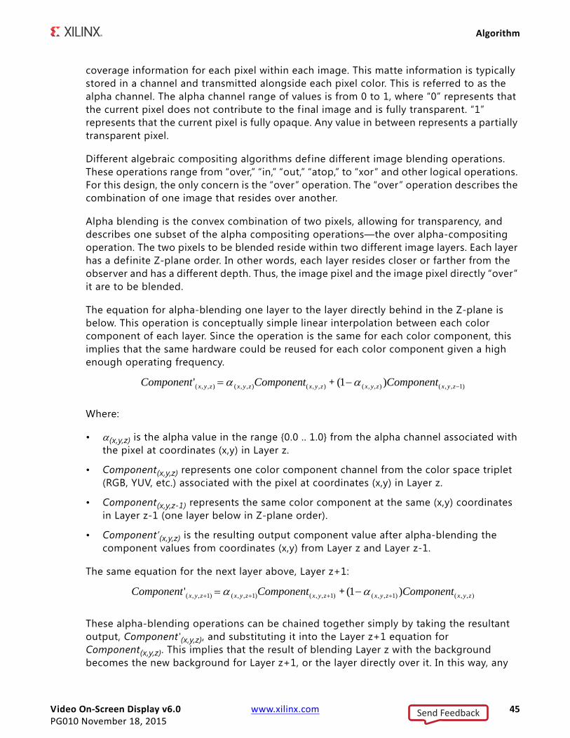
Video On‐Screen Display v6.0 www.xilinx.com 45PG010 November 18, 2015
Algorithm
coverage information for each pixel within each image. This matte information is typically stored in a channel and transmitted alongside each pixel color. This is referred to as the alpha channel. The alpha channel range of values is from 0 to 1, where “0” represents that the current pixel does not contribute to the f inal image and is fully transparent. “1” represents that the current pixel is fully opaque. Any value in between represents a partially transparent pixel.
Different algebraic compositing algorithms define different image blending operations. These operations range from “over,” “in,” “out,” “atop,” to “xor” and other logical operations. For this design, the only concern is the “over” operation. The “over” operation describes the combination of one image that resides over another.
Alpha blending is the convex combination of two pixels, allowing for transparency, and describes one subset of the alpha compositing operations—the over alpha-compositing operation. The two pixels to be blended reside within two different image layers. Each layer has a definite Z-plane order. In other words, each layer resides closer or farther from the observer and has a different depth. Thus, the image pixel and the image pixel directly “over” it are to be blended.
The equation for alpha-blending one layer to the layer directly behind in the Z-plane is below. This operation is conceptually simple linear interpolation between each color component of each layer. Since the operation is the same for each color component, this implies that the same hardware could be reused for each color component given a high enough operating frequency.
Where:
• (x,y,z) is the alpha value in the range {0.0 .. 1.0} from the alpha channel associated with the pixel at coordinates (x,y) in Layer z.
• Component(x,y,z) represents one color component channel from the color space triplet (RGB, YUV, etc.) associated with the pixel at coordinates (x,y) in Layer z.
• Component(x,y,z-1) represents the same color component at the same (x,y) coordinates in Layer z-1 (one layer below in Z-plane order).
• Component’(x,y,z) is the resulting output component value after alpha-blending the component values from coordinates (x,y) from Layer z and Layer z-1.
The same equation for the next layer above, Layer z+1:
These alpha-blending operations can be chained together simply by taking the resultant output, Component'(x,y,z), and substituting it into the Layer z+1 equation for Component(x,y,z). This implies that the result of blending Layer z with the background becomes the new background for Layer z+1, or the layer directly over it. In this way, any
)1,,(),,(),,(),,(),,( )1(' zyxzyxzyxzyxzyx ComponentComponentComponent +
),,()1,,()1,,()1,,()1,,( )1(' zyxzyxzyxzyxzyx ComponentComponentComponent +
Send Feedback
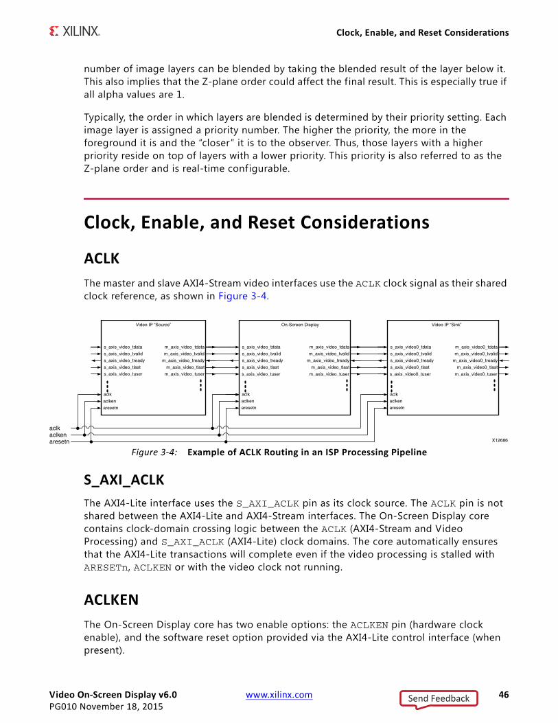
Video On‐Screen Display v6.0 www.xilinx.com 46PG010 November 18, 2015
Clock, Enable, and Reset Considerations
number of image layers can be blended by taking the blended result of the layer below it. This also implies that the Z-plane order could affect the f inal result. This is especially true if all alpha values are 1.
Typically, the order in which layers are blended is determined by their priority setting. Each image layer is assigned a priority number. The higher the priority, the more in the foreground it is and the “closer” it is to the observer. Thus, those layers with a higher priority reside on top of layers with a lower priority. This priority is also referred to as the Z-plane order and is real-time configurable.
Clock, Enable, and Reset Considerations
ACLK
The master and slave AXI4-Stream video interfaces use the ACLK clock signal as their shared clock reference, as shown in Figure 3-4.
S_AXI_ACLK
The AXI4-Lite interface uses the S_AXI_ACLK pin as its clock source. The ACLK pin is not shared between the AXI4-Lite and AXI4-Stream interfaces. The On-Screen Display core contains clock-domain crossing logic between the ACLK (AXI4-Stream and Video Processing) and S_AXI_ACLK (AXI4-Lite) clock domains. The core automatically ensures that the AXI4-Lite transactions will complete even if the video processing is stalled with ARESETn, ACLKEN or with the video clock not running.
ACLKEN
The On-Screen Display core has two enable options: the ACLKEN pin (hardware clock enable), and the software reset option provided via the AXI4-Lite control interface (when present).
X-Ref Target - Figure 3-4
Figure 3‐4: Example of ACLK Routing in an ISP Processing Pipeline
Send Feedback

Video On‐Screen Display v6.0 www.xilinx.com 47PG010 November 18, 2015
Clock, Enable, and Reset Considerations
ACLKEN is by no means synchronized internally to AXI4-Stream frame processing therefore de-asserting ACLKEN for extended periods of time may lead to image tearing.
The ACLKEN pin facilitates:
• Multi-cycle path designs (high speed clock division without clock gating),
• Standby operation of subsystems to save on power
• Hardware controlled bring-up of system components
IMPORTANT: To prevent transaction errors when ACLKEN (clock enable) pins are used (toggled) in conjunction with a common clock source driving the master and slave sides of an AXI4-Stream interface, the ACLKEN pins associated with the master and slave component interfaces must also be driven by the same signal.
S_AXI_ACLKEN
The S_AXI_ACLKEN is the clock enable signal for the AXI4-Lite interface only. Driving this signal low will only affect the AXI4-Lite interface and will not halt the video processing in the ACLK clock domain.
ARESETn
The On-Screen Display core has two reset source: the ARESETn pin (hardware reset), and the software reset option provided via the AXI4-Lite control interface (when present).
CAUTION! ARESETn is not synchronized internally to AXI4-Stream frame processing. Therefore, de-asserting ARESETn while a frame is being process leads to image tearing.
The external reset pulse needs to be held for 32 ACLK cycles to reset the core. The ARESETn signal will only reset the AXI4-Stream interfaces. The AXI4-Lite interface is unaffected by the ARESETn signal to allow the video processing core to be reset without halting the AXI4-Lite interface.
IMPORTANT: When resetting a system with multiple-clocks and corresponding reset signals, the reset generator must ensure that all reset signals are asserted/de-asserted long enough for all interfaces and clock-domains in all IP cores to correctly reinitialize.
S_AXI_ARESETn
The S_AXI_ARESETn signal is synchronous to the S_AXI_ACLK clock domain, but is internally synchronized to the ACLK clock domain. The S_AXI_ARESETn signal will reset the entire core including the AXI4-Lite and AXI4-Stream interfaces.
Send Feedback
Video On‐Screen Display v6.0 www.xilinx.com 48PG010 November 18, 2015
System Considerations
System ConsiderationsThe On-Screen Display core must be configured for the actual image frame-size to operate properly. To gather the frame size information from the incoming video stream, it can be connected to the Video In to AXI4-Stream input and the Video Timing Controller. The timing detector logic in the Video Timing Controller will gather the image sensor timing signals. The AXI4-Lite control interface on the Video Timing Controller allows the system processor to read out the measured frame dimensions, and program all downstream cores, such as the On-Screen Display, with the appropriate image dimensions.
If the target system uses only one configuration of the On-Screen Display (i.e. does not need to be reprogrammed ever), you may choose to create a constant configuration by removing the AXI4-Lite interface. This reduces the core Slice footprint.
Clock Domain Interaction
The ARESETn and ACLKEN input signals will not reset or halt the AXI4-Lite interface. This allows the video processing to be reset or halted separately from the AXI4-Lite interface without disrupting AXI4-Lite transactions.
IMPORTANT: The AXI4-Lite interface will respond with an error if the core registers cannot be read or written within 128 S_AXI_ACLK clock cycles. The core registers cannot be read or written if the ARESETn signal is held low, if the ACLKEN signal is held low or if the ACLK signal is not connected or not running. If core register read does not complete, the AXI4-Lite read transaction will respond with 10 on the S_AXI_RRESP bus. Similarly, if a core register write does not complete, the AXI4-Lite write transaction will respond with 10 on the S_AXI_BRESP bus. The S_AXI_ARESETn input signal resets the entire core.
Programming Sequence
If processing parameters such as the image size needs to be changed on the fly, or the system needs to be reinitialized, it is recommended that pipelined Video IP cores are disabled/reset from system output towards the system input, and programmed/enabled from system input to system output. STATUS register bits allow system processors to identify the processing states of individual constituent cores, and successively disable a pipeline as one core after another is f inished processing the last frame of data.
Send Feedback

Video On‐Screen Display v6.0 www.xilinx.com 49PG010 November 18, 2015
Chapter 4
Customizing and Generating the CoreThis chapter includes information about using Xilinx tools to customize and generate the core in the Vivado® Design Suite environment.
Vivado Integrated Design Environment (IDE)You can customize the IP for use in your design by specifying values for the various parameters associated with the IP core using the following steps:
1. Select the IP from the IP catalog.
2. Double-click on the selected IP or select the Customize IP command from the toolbar or popup menu.
For details, see the sections, “Working with IP” and “Customizing IP for the Design” in the Vivado Design Suite User Guide: Designing with IP (UG896) [Ref 3] and the “Working with the Vivado IDE” section in the Vivado Design Suite User Guide: Getting Started (UG910) [Ref 5].
If you are customizing and generating the core in the Vivado IP Integrator, see the Vivado Design Suite User Guide: Designing IP Subsystems Using IP Integrator (UG994) [Ref 7] for detailed information. IP Integrator might auto-compute certain configuration values when validating or generating the design. To check whether the values do change, see the description of the parameter in this chapter. To view the parameter value you can run the validate_bd_design command in the Tcl console.
Note: Figures in this chapter are illustrations of the Vivado IDE. This layout might vary from the current version.
InterfaceThe Video On-Screen Display core is easily configured to meet the developer's specific needs through the Vivado interface shown in Figure 4-1, Figure 4-2, and Figure 4-3. This section provides a quick reference to parameters that can be configured at generation time.
Send Feedback

Video On‐Screen Display v6.0 www.xilinx.com 50PG010 November 18, 2015
Interface
X-Ref Target - Figure 4-1
Figure 4‐1: Vivado IP Catalog GUI ‐ Main Window
Send Feedback

Video On‐Screen Display v6.0 www.xilinx.com 51PG010 November 18, 2015
Interface
X-Ref Target - Figure 4-2
Figure 4‐2: Vivado IP Catalog GUI ‐ Constant Mode Options Window
Send Feedback

Video On‐Screen Display v6.0 www.xilinx.com 52PG010 November 18, 2015
Interface
Note: The Graphics Controller Options Window is available only if the Layer Type is set to “Internal Graphics Controller.”
Global Parameters
• Component Name: The component name is used as the base name of output files generated for the module. Names must begin with a letter and must be composed from characters: a to z, 0 to 9and “_”. The name v_osd_v6_0 is not allowed.
• Optional Features:
° Include AXI4-Lite Interface: When selected, the core will be generated with an AXI4-Lite interface, which gives access to dynamically program and change processing parameters. For more information, refer to Chapter 2, Core Interfaces.
° Include INTC Interface: When selected, the core will generate the optional INTC_IF port, which gives parallel access to signals indicating frame processing status and error conditions. For more information, refer to Interrupts in Chapter 2.
• Video Format: This f ield configures the input format of the AXI4-Stream interfaces. Valid values are YUV 422, YUV 444, RGB, YUVa 422, YUVa 444 and RGBa. When using IP Integrator, this parameter is automatically computed based on the Video Format of the video IP cores connected to the slave AXI-Stream video interfaces.
X-Ref Target - Figure 4-3
Figure 4‐3: Vivado IP Catalog GUI ‐ Graphics Controller Options Window
Send Feedback

Video On‐Screen Display v6.0 www.xilinx.com 53PG010 November 18, 2015
Interface
Note: If the input is YUVa 422, YUVa 444 or RGBa the output will be YUV 422, YUV 444 or RGB respectively (no alpha on output stream).
• Video Component Width: This f ield configures the data width of each color component channel. Valid values are 8, 10 and 12. Configuring the Video Component Width and the Video Format yields an effective bits per pixel of 16, 24, 32, 40 or 48 bits. When using IP Integrator, this parameter is automatically computed based on the Video Component Width of the video IP cores connected to the slave AXI-Stream video interfaces.
• Number of Layers: This f ield configures the number of layers to alpha blend together. Each layer can be configured to read data from the FIFO inputs or from one of the internal Graphics Controllers. Valid range is (1 .. 8).
• Maximum Screen Width: This f ield configures the maximum allowed screen size. The Maximum screen width is configurable. Changing this f ield affects several counters, comparators and memory (Block RAM) usage. Increased screen size increases resource usage. Valid range for Screen Width is {128 .. 4095}.
• Layer Configuration – Layer # Type: These f ields configure the type, or data source, of each layer, one f ield for each layer. Each layer is numbered from 0 to 7. The maximum number of layers is set by the Number of Layers f ield. Three data sources are valid:
° External AXIS: This is an input AXI4-Stream slave interface with tdata, tvalid, tready and tlast. See Input AXI4-Stream Slave Interface(s) in Chapter 2.
° Internal Graphics Controller: If the layer is configured for this type, then the AXI4-Stream slave interfaces are removed and all data is generated and read from an internal Graphics Controller.
Screen Layout Parameters
• Background Size:
° Width: This f ield configures the horizontal size of the background.
° Height: This f iled configures the vertical size of the background.
• Background Color: The fields configure the default background color.
• Layer:
° Horizontal Position: This f ield configures the horizontal position, starting from pixel 0, of the upper left corner of each layer.
° Vertical Position: This f ield configures the vertical position, starting from line 0, of the upper left corner of each layer.
• Width: This f ield configures the horizontal size of each layer.
• Height: This f ield configures the vertical size of each layer.
Send Feedback

Video On‐Screen Display v6.0 www.xilinx.com 54PG010 November 18, 2015
Interface
• Layer Priority: These fields configure the Z-plane order of each layer. Layers with higher priority will be on-top layers with lower priority. Each layer must have a unique priority setting.
• Layer Enable: These fields configure if a layer is enabled or disabled by default.
• Global Alpha Value: These f ields configure the Alpha Value used for the entire layer.
Note: This should be used if no Alpha is supplied with the AXI4-Stream input.
• Global Alpha Enable: These f ields enable or disable the use of the global alpha value for the given layer. If the Global Alpha Enable is disabled, then the alpha-value supplied from the AXI4-Stream input (for each pixel) is used.
Note: Graphics Controller Layers should not have the Global Alpha enabled.
Graphics Controller Parameters
• Instructions: This f ield configures the maximum number of Graphics Controller instructions that can be executed per frame. Increasing this number increases the number of Block RAMs utilized.
• Instruction Set: This f ield configures which instructions are valid for the Graphics Controller implementation. Two instructions are currently configurable: box and text. Other instructions, including NoOp, are always available.
• Number of Colors: This f ield configures the size of the color palette used by the Graphics Controller. Valid values are 16 and 256.
• Color Memory Type: This f ield configures how the color palette is implemented in hardware, as Distributed RAM, as Block RAM or Auto-Configured. In auto-configuration mode, distributed RAM will be used if the color palette is small enough. The RAM type can be overridden if it is known which type is preferred for the application.
• Number of Characters: This f ield configures the number of characters to be stored within the internal Font RAM. Valid values are 1 to 256. This f ield, along with the Character Width, Character Height, ASCII Offset and Bit per Pixel f ields, affects the overall size of the Font RAM.
• Character Width: This f ield configures the width of each character. The width is in pixels. Valid values are 8 and 16.
• Character Height: This f ield configures the height of each character. The height is in video lines. Valid values are 8 and 16.
• ASCII Offset: This f ield configures the ASCII value of the f irst location in the Font RAM. This is useful if it is known that certain ASCII values will not be used.
• Bits per Pixel: This f ield configures the bits per pixel of each character. Valid values are 1 and 2.
° 1 = One bit per pixel. This yields a foreground and a background color for each character.
Send Feedback

Video On‐Screen Display v6.0 www.xilinx.com 55PG010 November 18, 2015
Output Generation
° 2 = Two bits per pixel. This allows each character pixel to be programmed to one of four different colors.
• Number of Strings: This f ield configures the maximum number of strings to be stored within the Text RAM. This f ield, along with the Maximum String Length field, affects the overall size of the Text RAM. The maximum number of strings cannot exceed 256.
• Maximum String Length: This f ield configures the maximum string length allowed for each string within the Text RAM. Valid values are 32, 64, 128 and 256.
Output GenerationFor details, see “Generating IP Output Products” in the Vivado Design Suite User Guide: Designing with IP (UG896).
Send Feedback

Video On‐Screen Display v6.0 www.xilinx.com 56PG010 November 18, 2015
Chapter 5
Constraining the Core
Required ConstraintsThe only constraints required are clock frequency constraints for the video clock, aclk , and the AXI4-Lite clock, s_axi_aclk . Paths between the two clock domains should be constrained with a max_delay constraint and use the datapathonly flag, causing setup and hold checks to be ignored for signals that cross clock domains. These constraints are provided in the XDC constraints f ile included with the core.
Send Feedback

Video On‐Screen Display v6.0 www.xilinx.com 57PG010 November 18, 2015
Chapter 6
SimulationThis chapter contains information about simulating IP in the Vivado® Design Suite environment. For comprehensive information about Vivado simulation components, as well as information about using supported third party tools, see the Vivado Design Suite User Guide: Logic Simulation (UG900) [Ref 6].
Send Feedback

Video On‐Screen Display v6.0 www.xilinx.com 58PG010 November 18, 2015
Chapter 7
Synthesis and ImplementationFor details about synthesis and implementation, see “Synthesizing IP” and “Implementing IP” in the Vivado Design Suite User Guide: Designing with IP (UG896) [Ref 3].
Send Feedback
Video On‐Screen Display v6.0 www.xilinx.com 59PG010 November 18, 2015
Chapter 8
C Model ReferenceThe Xilinx LogiCORE ™ IP Video OSD has a bit accurate C model for 32-bit Windows, 64-bit Windows, 32-bit Linux and 64-bit Linux platforms. The model has an interface consisting of a set of C functions, which reside in a statically link library (shared library). Full details of the interface are given in Interface, page 61. An example piece of C code is provided in Example Code, page 71 to show how to call the model.
The model is bit accurate, as it produces exactly the same output data as the core on a frame-by-frame basis. However, the model is not cycle accurate, as it does not model the core's latency or its interface signals. The latest version of the model is available for download on the Xilinx LogiCORE IP Video OSD web page at:
http://www.xilinx.com/products/ipcenter/EF-DI-OSD.htm
Unpacking and Model ContentsUnzip the v_osd_v6_0_bitacc_model.zip f ile, containing the bit accurate models for the On-Screen Display IP Core. This creates the directory structure and files in Table 8-1.
Table 8‐1: Directory Structure and Files of the Video On‐Screen Display v6.0 Bit Accurate C Model
File Name Contents
/doc C Model documentation
README.txt Release notes
pg010_v_osd.pdf LogiCORE IP Video On-Screen Display Product Guide
Makefile Makefile for running GCC via make for 32-bit and 64-bit Linux platforms
v_osd_v6_0_bitacc_cmodel.h Model header f ile
rgb_utils.h Header f ile declaring the RGB image/video container type and support functions
yuv_utils.h Header f ile declaring the YUV (.yuv) image f ile I/O functions
bmp_utils.h Header f ile declaring the bitmap (.bmp) image f ile I/O functions
video_utils.h Header file declaring the generalized image/video container type, I/O and support functions
Send Feedback

Video On‐Screen Display v6.0 www.xilinx.com 60PG010 November 18, 2015
Unpacking and Model Contents
video_fio.h Header f ile declaring support functions for test bench stimulus file I/O
run_bitacc_cmodel.c Example code calling the C model
run_bitacc_cmodel_config.c Example code calling the C model; uses command line and config file arguments
/lin64 Precompiled bit accurate ANSI C reference model for simulation on 64-bit Linux platforms
libIp_v_osd_v6_0_bitacc_cmodel.so Model shared object library
run_bitacc_cmodel 64-bit Linux f ixed configuration executable
run_bitacc_cmodel_config 64-bit Linux programmable configuration executable
/lin Precompiled bit accurate ANSI C reference model for simulation on 32-bit Linux platforms.
libIp_v_osd_v6_0_bitacc_cmodel.so Model shared object library
run_bitacc_cmodel 32-bit Linux f ixed configuration executable
run_bitacc_cmodel_config 32-bit Linux programmable configuration executable
/nt64 Precompiled bit accurate ANSI C reference model for simulation on 64-bit Windows platforms
libIp_v_osd_v6_0_bitacc_cmodel.lib Precompiled library f ile for 64-bit Windows platforms compilation
run_bitacc_cmodel.exe 64-bit Windows f ixed configuration executable
run_bitacc_cmodel_config.exe 64-bit Windows programmable configuration executable
/nt Precompiled bit accurate ANSI C reference model for simulation on 32-bit Windows platforms
libIp_v_osd_v6_0_bitacc_cmodel.lib Precompiled library f ile for 32-bit Windows platforms compilation
run_bitacc_cmodel.exe 32-bit Windows f ixed configuration executable
run_bitacc_cmodel_config.exe 32-bit Windows programmable configuration executable
examples Example input f iles to be used with the run_bitacc_cmodel_config executable
example0.cfg Example config file; internal test patterns, no graphics controller and BMP output
example1.cfg Example config file; no input, internal test patterns , no graphics controller and YUV output
example2.cfg Example config file; BMP input, no graphics controller and BMP output
example3.cfg Example config file., BMP input, graphics overlay and BMP output
clut.txt Example graphics controller color look-up table/pallet f ile
string.txt Example graphics controller text/strings file
Table 8‐1: Directory Structure and Files of the Video On‐Screen Display v6.0 Bit Accurate C Model
File Name Contents
Send Feedback

Video On‐Screen Display v6.0 www.xilinx.com 61PG010 November 18, 2015
Installation
InstallationFor Linux, make sure the following f iles are in a directory in the $LD_LIBRARY_PATH environment variable:
• libIp_v_osd_v6_0_bitacc_cmodel.so
Software Requirements The Video On-Screen Display C models were compiled and tested with the software listed in Table 8-2.
InterfaceThe video OSD bit accurate C model core function is a statically linked library. This model is accessed through a set of functions and data structures that are declared in the v_osd_v6_0_bitacc_cmodel.h f ile. A higher level software project can make function calls to this function:
/** * Create a new state structure for this C-Model. * * IMPORTANT: Client is responsible for calling * xilinx_ip_v_osd_v6_0_destroy_state() * to free state memory. * * at theparam generics Generics to be used to configure C-Model * state.
font.txt Example graphics controller font f ile
instructions.txt Example graphics controller instruction list
bridge.bmp Example 24-bit 576x720 bitmap
Table 8‐1: Directory Structure and Files of the Video On‐Screen Display v6.0 Bit Accurate C Model
File Name Contents
Table 8‐2: Compilation Tools for the Bit Accurate C Models
Platform C Compiler
Linux 32-bit and 64-bit GCC 3.4.6 & 4.1.6
Windows 32-bit and 64-bit Microsoft Visual Studio 2008
Send Feedback

Video On‐Screen Display v6.0 www.xilinx.com 62PG010 November 18, 2015
Interface
* * @returns xilinx_ip_v_osd_v6_0_state* Pointer to the internal * state. */struct xilinx_ip_v_osd_v6_0_state*xilinx_ip_v_osd_v6_0_create_state(struct xilinx_ip_v_osd_v6_0_generics generics);
/** * Simulate this bit-accurate C-Model. * * @param state Internal state of this C-Model. State * may span multiple simulations. * @param inputs Inputs to this C-Model. * @param outputs Outputs from this C-Model. * * @returns Exit code Zero for SUCCESS, Non-zero otherwise. */int xilinx_ip_v_osd_v6_0_bitacc_simulate( struct xilinx_ip_v_osd_v6_0_state* state, struct xilinx_ip_v_osd_v6_0_inputs inputs, struct xilinx_ip_v_osd_v6_0_outputs* outputs);
Before using the model, the structures holding the generics, inputs, and outputs of the OSD instance must be defined:
struct xilinx_ip_v_osd_v6_0_generics generics;struct xilinx_ip_v_osd_v6_0_inputs inputs;struct xilinx_ip_v_osd_v6_0_outputs outputs;
The declaration of these structures is in the v_osd_v6_0_bitacc_cmodel.h f ile.
Before making the function call, complete these steps:
1. Populate the generics structure. It defines the values of build time parameters. See OSD Generics Structure for more information on the structure and an example of how to initialize.
2. Populate the inputs structure. It defines the values of run time parameters. See OSD Inputs Structure for more information on the structure and an example of how to initialize.
3. Populate the outputs structure. See OSD Outputs Structure for more information on the structure and an example of how to initialize.
After the inputs are defined and all video_structs are initialized, the model can be simulated by calling the following functions:
state = xilinx_ip_v_osd_v6_0_create_state(generics); if (state == NULL) { printf(“ERROR: could not create state object\n”); return 1; }
// Simulate the core
Send Feedback

Video On‐Screen Display v6.0 www.xilinx.com 63PG010 November 18, 2015
Interface
printf(“Running the C model...\n”); if(xilinx_ip_v_osd_v6_0_bitacc_simulate(state, inputs, &outputs) != 0) { printf(“ERROR: simulation did not complete successfully\n”); return 1; } else { printf(“Simulation completed successfully\n”); }
The results are provided in the outputs structure, which contains only one member of type video_struct. See OSD Video Structure for more information on video_struct.
The successful execution of all provided functions return a value of 0, otherwise a non-zero error code indicates that problems occurred during function calls.
OSD Generics Structure
The Xilinx LogiCORE IP Video OSD Core bit accurate C model takes multiple generic parameters. All generic parameters are integers or integer arrays. See Table 8-3 for generic definitions.
Table 8‐3: OSD Generics Structure
Generic Designation
C_DATA_WIDTH Data width of each color component channel; valid values are 8, 10 and 12.
C_NUM_LAYERS The number of layers.
C_LAYER_TYPE[8] Defines the layer type of each layer:
• 1=Graphics Controller
• 2=AXI4-Stream
All other values are reserved.
C_LAYER_INS_BOX_EN[8] Enable box instructions.
C_LAYER_INS_TEXT_EN[8] Enable text instructions.
C_LAYER_CLUT_SIZE[8] Maximum number of colors.
C_LAYER_TEXT_NUM_STRINGS[8] Maximum number of strings.
C_LAYER_TEXT_MAX_STRING_LENGTH[8] Maximum string length.
C_LAYER_FONT_NUM_CHARS[8] Maximum number of characters.
C_LAYER_FONT_WIDTH[8] Maximum font width.
C_LAYER_FONT_HEIGHT[8] Maximum font height.
C_LAYER_FONT_BPP[8] Font bits per pixel.
C_LAYER_FONT_ASCII_OFFSET[8] The ASCII value of the f irst character in the font file.
Send Feedback

Video On‐Screen Display v6.0 www.xilinx.com 64PG010 November 18, 2015
Interface
Calling xilinx_ip_v_osd_v6_0_get_default_generics() initializes the generics structure, xilinx_ip_v_osd_v6_0_generics, with the OSD defaults. An example of initialization of the generics structure with layer two configured as a graphics controller is as follows:
generics = xilinx_ip_v_osd_v6_0_get_default_generics(); //Get Defaults generics.C_NUM_LAYERS = 3; generics.C_LAYER_TYPE[2] = 1; // Graphics Controller // Setup Graphics Controller generics.C_LAYER_INS_BOX_EN[2] = 1; generics.C_LAYER_INS_TEXT_EN[2] = 1; generics.C_LAYER_CLUT_SIZE[2] = 256;
// Setup Font RAM generics.C_LAYER_FONT_NUM_CHARS[2] = 128; generics.C_LAYER_FONT_WIDTH[2] = 8; generics.C_LAYER_FONT_HEIGHT[2] = 8; generics.C_LAYER_FONT_BPP[2] = 1; generics.C_LAYER_FONT_ASCII_OFFSET[2] = 0;
// Setup Text RAM generics.C_LAYER_TEXT_NUM_STRINGS[2] = 16; // Set number of strings generics.C_LAYER_TEXT_MAX_STRING_LENGTH[2] = 64; //Set max string length
OSD Inputs Structure
The structure xilinx_ip_v_osd_v6_0_inputs defines the values of run time parameters and the actual input video frames/images for each layer.
struct xilinx_ip_v_osd_v6_0_inputs{ struct video_struct video_in[OSD_MAX_LAYERS];
struct frame_cfg_struct * frame_cfg; struct layer_cfg_struct *layer_cfg[OSD_MAX_LAYERS]; struct graphics_cfg_struct * gfx_cfg[OSD_MAX_LAYERS]; int num_frames; int color_space;
}; // end xilinx_ip_v_osd_v6_0_inputs
The video_in variable is an array of video_struct structures, one structure per layer. See the OSD Video Structure for a description of the video_in structure. The video_in structure must be initialized if neither the internal graphics controller nor the test pattern generator is used.
Frame Configuration
The frame_cfg variable is a pointer to the frame_cfg_struct. The frame_cfg_struct is defined as:
Send Feedback
Video On‐Screen Display v6.0 www.xilinx.com 65PG010 November 18, 2015
Interface
struct frame_cfg_struct{ int y_size; int x_size; int bg_color[3];
struct frame_cfg_struct * next; // For Changing parameters each Frame};
The frame_cfg variable points to the first element in the frame config linked list. For each frame, the OSD model reads the x and y size of output frame and the background color from the frame_cfg_struct pointed to by frame_cfg. At the end of the frame, if the next pointer is not NULL, the OSD model updates the background color and the output size from the next structure in the linked list. Consequently, if the number of video frames is more than the number of elements in the linked list, the last element is used for the remaining frames. The user is responsible for initializing the linked list.
Layer Configuration
The layer_cfg variable is an array of pointers to the layer_cfg_struct structure, one pointer per layer. The layer_cfg_struct is defined as:
struct layer_cfg_struct{ int enable; int g_alpha_en; int priority; int alpha; int x_pos; int y_pos; int x_size; int y_size; int chan_mode[4]; int chan_color[4];
struct layer_cfg_struct * next; // For Changing parameters each Frame};
Each pointer must be initialized to point to the first element in the layer config linked list. For each frame, the OSD model reads the layer registers and the test parameter arrays (chan_mode[4] and chan_color[4]) from the layer_cfg_struct pointed to by the layer_cfg pointer. This linked list enables the user to change the layer configuration (size, position, transparency, z-plane, and so on) for each video frame.
At the end of the frame, if the next pointer is not NULL, the OSD model updates the layer configuration from the next structure in the linked list. Consequently, if the number of video frames is more than the number of elements in the linked list, the last element is used for the remaining frames. The user is responsible for initializing the linked list.
Send Feedback

Video On‐Screen Display v6.0 www.xilinx.com 66PG010 November 18, 2015
Interface
Graphics Configuration
The gfx_cfg variable is an array of pointers to the graphics_cfg_struct structure, one pointer per layer. This variable is only used if the layer is configured for graphics controller input. The graphics_cfg_struct is defined as:
struct graphics_cfg_struct{ int layer_num;
uint16 * clut; // Color Table char * text_ram; // Text Ram int * font_ram; // Font Ram
struct graphics_list * graph_instruction;
struct graphics_cfg_struct * next; // For Changing parameters each Frame};
Each pointer must be initialized to point to the f irst element in the graphics config linked list. For each frame, the OSD model reads the graphics controller memories from the graphics_cfg_struct pointed to by the gfx_cfg pointer. This linked list enables the user to change the graphics controller output (boxes, text, color, size, position, transparency, font and strings) for each video frame.
The CLUT pointer points to an array of 16-bit unsigned integers. This array contains the color entries for the current video frame. Each color entry contains four integers, one for each color component and one for alpha. The CLUT array must contain 4*16 or 4*256 integers.
The text_ram pointer points to an array of characters. This array contains all strings for the current video frame. The number of characters in the array must equal the (maximum string length) * (the number of strings).
The font_ram pointer points to an array of integers. This array contains the font for the current video frame. The number of integers in the array must equal the (number of characters) * (font width) * (font height). The number of bits used in each integer is 8, 16 or 32 depending on the setting of the font_width and font_bpp.
The graph_instruction pointer points to a linked list of graphics instructions (defined by the graphics_list structure). This linked list contains the graphics instructions for the current video frame. The Graphics Controller draws each instruction in the linked list until a NULL pointer is encountered. The graphic_list structure is defined as:
struct graphics_list{ int opcode; int xstart; int xstop; int ystart; int ystop; int color_index;
Send Feedback

Video On‐Screen Display v6.0 www.xilinx.com 67PG010 November 18, 2015
Interface
int text_index; int object_size; struct graphics_list * next;
};
This structure contains the same fields as in the instruction file defined previously. The opcode variable can be OSD_INS_BOX, OSD_INS_TEXT or OSD_INS_BOXTEXT (each defined in the v_osd_v_2_0_bitacc_cmodel.h f ile). See Table D-1, page 106 through Table D-5, page 109 for more information on xstart, xstop, ystart, ystop, color_index and text_index definitions.
At the end of the frame, if the next pointer is not NULL, the OSD model updates the graphics controller configuration from the next structure in the linked list. Consequently, if the number of video frames is more than the number of elements in the linked list, the last element is used for the remaining frames. The user is responsible for initializing the linked list. Example initialization code of the inputs structure is as follows:
inputs.frame_cfg = (struct frame_cfg_struct *) calloc(1, sizeof(struct frame_cfg_struct)); inputs.frame_cfg->x_size = 1280; inputs.frame_cfg->y_size = 720; inputs.frame_cfg->bg_color[0] = 0x88; inputs.frame_cfg->bg_color[1] = 0x3a; inputs.frame_cfg->bg_color[2] = 0xbd; inputs.frame_cfg->next = NULL; // End of Frame Config
// Setup Layer 0 Configuration inputs.layer_cfg[0] = (struct layer_cfg_struct *) calloc(1, sizeof(struct layer_cfg_struct)); inputs.layer_cfg[0]->enable = 1; inputs.layer_cfg[0]->g_alpha_en = 0; inputs.layer_cfg[0]->priority = 2; inputs.layer_cfg[0]->alpha = 0x80; inputs.layer_cfg[0]->x_pos = 0; inputs.layer_cfg[0]->y_pos = 0; inputs.layer_cfg[0]->x_size = 1280; inputs.layer_cfg[0]->y_size = 720; inputs.layer_cfg[0]->chan_mode[0] = OSD_SOLID_MODE; inputs.layer_cfg[0]->chan_mode[1] = OSD_SOLID_MODE; inputs.layer_cfg[0]->chan_mode[2] = OSD_SOLID_MODE; inputs.layer_cfg[0]->chan_mode[3] = OSD_HRAMP_MODE;
inputs.layer_cfg[0]->chan_color[0] = 0xe0; inputs.layer_cfg[0]->chan_color[1] = 0x5a; inputs.layer_cfg[0]->chan_color[2] = 0xbf; inputs.layer_cfg[0]->chan_color[3] = 0x80; // Alpha inputs.layer_cfg[0]->next = NULL;
Send Feedback
Video On‐Screen Display v6.0 www.xilinx.com 68PG010 November 18, 2015
Interface
OSD Outputs Structure
The structure xilinx_ip_v_osd_v6_0_outputs provides the actual output video frames/images of the OSD core. This structure is a wrapper to the standard video_struct used by other Xilinx video core C models.
struct xilinx_ip_v_osd_v6_0_outputs{ struct video_struct video_out;}; // xilinx_ip_v_osd_v6_0_outputs
The video_out structure must be initialized. The following code shows a typical video_out initialization.
// Setup Output Video Buffer outputs.video_out.frames = inputs.num_frames; outputs.video_out.rows = inputs.frame_cfg->y_size; outputs.video_out.cols = inputs.frame_cfg->x_size; outputs.video_out.mode = FORMAT_C444; outputs.video_out.bits_per_component = generics.C_DATA_WIDTH; outputs.video_out.data[0] = NULL; outputs.video_out.data[1] = NULL; outputs.video_out.data[2] = NULL;
OSD Video Structure
Input images or video streams can be provided to the OSD v6.0 reference model using the video_struct structure, defined in video_utils.h. Output images or video streams are also placed within a video_struct structure. The video_struct is defined as:
struct video_struct{ int frames, rows, cols, bits_per_component, mode; uint16*** data[5]; };
The structure member variables are defined in Table 8-4.
Table 8‐4: Member Variables of the Video Structure
Member Variable Designation
frames Number of video/image frames in the data structure
rows Number of rows per framePertains to the image plane with the most rows and columns, such as the luminance channel for YUV data. Frame dimensions are assumed constant through the all frames of the video stream, however different planes, such as y, u and v can have different smaller dimensions.
cols Number of columns per framePertains to the image plane with the most rows and columns, such as the luminance channel for YUV data. Frame dimensions are assumed constant through the all frames of the video stream, however different planes, such as y, u and v can have different smaller dimensions.
Send Feedback
Video On‐Screen Display v6.0 www.xilinx.com 69PG010 November 18, 2015
Interface
Note: The OSD core supports four formats: FORMAT_RGB, FORMAT_C444, FORMAT_C422, and FORMAT_C420.
Working With Video_struct Containers
The video_utils.h f ile defines functions to simplify access to video data in video_struct.
int video_planes_per_mode(int mode);int video_rows_per_plane(struct video_struct* video, int plane);int video_cols_per_plane(struct video_struct* video, int plane);
Function video_planes_per_mode returns the number of component planes defined by the mode variable, as described in Table 8-5. Functions video_rows_per_plane and video_cols_per_plane return the number of rows and columns in a given plane of the selected video structure. The following example demonstrates using these functions in conjunction to process all pixels within a video stream stored in variable in_video, with this construct:
bits_per_component Number of bits per color channel/component. All image planes are assumed to have the same color/component representation. Maximum number of bits per component is 16.
mode Contains information about the designation of data planes. Named constants to be assigned to mode are listed in Table 8-5.
data Set of 5 pointers to 3 dimensional arrays containing data for image planes. data is in 16 bit unsigned integer format accessed as data[plane][frame][row][col]
Table 8‐5: Named Constants for Video Modes With Corresponding Planes and Representations
Mode Planes Video Representation
FORMAT_MONO 1 Monochrome – luminance only
FORMAT_RGB 3 RGB image/video data
FORMAT_C444 3 444 YUV, or YCrCb image/video data
FORMAT_C422 3 422 format YUV video, (u, v chrominance channels horizontally sub-sampled)
FORMAT_C420 3 420 format YUV video, ( u, v sub-sampled both horizontally and vertically )
FORMAT_MONO_M 3 Monochrome (luminance) video with motion
FORMAT_RGBA 4 RGB image/video data with alpha (transparency) channel
FORMAT_C420_M 5 420 YUV video with motion or alpha
FORMAT_C422_M 5 422 YUV video with motion or alpha
FORMAT_C444_M 5 444 YUV video with motion or alpha
FORMAT_RGBM 5 RGB video with motion
Table 8‐4: Member Variables of the Video Structure (Cont’d)
Send Feedback
Video On‐Screen Display v6.0 www.xilinx.com 70PG010 November 18, 2015
Example Code
for (int frame = 0; frame < in_video->frames; frame++) { for (int plane = 0; plane < video_planes_per_mode(in_video->mode); plane++) { for (int row = 0; row < rows_per_plane(in_video,plane); row++) { for (int col = 0; col < cols_per_plane(in_video,plane); col++) {
// User defined pixel operations on // in_video->data[plane][frame][row][col] } } }}
Delete the Video Structure
Finally, large arrays such as the video_in element in the video structure must be deleted to free up memory. As an example, the following function is defined as part of the video_utils package.
void free_video_buff(struct video_struct* video ) { int plane, frame, row;
if (video->data[0] != NULL) { for (plane = 0; plane <video_planes_per_mode(video->mode); plane++) { for (frame = 0; frame < video->frames; frame++) { for (row = 0; row<video_rows_per_plane(video,plane); row++) { free(video->data[plane][frame][row]); } free(video->data[plane][frame]); } free(video->data[plane]); } } }
This function can be called in the following way to free the video input buffers (up to eight) and the video output buffer:
// Free Layer Buffers for(i=0; i < generics.C_NUM_LAYERS; i++) { printf(“Freeing Layer Video Buffer #%d...\n”, i); free_video_buff(&inputs.video_in[i]); } printf(“Freeing Output Buffer...\n”); free_video_buff(&outputs.video_out);
Example CodeTwo example C f iles, run_bitacc_cmodel.c and bitacc_cmodel_config.c,are provided. The 32-bit and 64-bit Windows and Linux executables for these examples are also included. This C file has these characteristics:
Send Feedback
Video On‐Screen Display v6.0 www.xilinx.com 71PG010 November 18, 2015
Example Code
The run_bitacc_cmodel example executable provides:
• Shows a f ixed implementation of the OSD, including two AXI4-Stream layers populated from the internal test pattern generator and one graphics controller layer.
• Contains an example of how to write an application that makes all necessary function calls to the OSD C model core function.
• Contains an example of how to populate the video structures at the input and output, including allocation of memory to these structures.
• Uses a YUV file reading function to extract video information from YUV files for use by the model.
• Uses a YUV file writing function to provide an output YUV file, which allows the user to visualize the result of the core.
The run_bitacc_cmodel example executable does not use command line parameters. To run the executable:
1. Use the cd command to go to the platform directory (lin64, lin, win64 or win32).
2. Enter this command at the shell or DOS prompt:
run_bitacc_cmodel
The run_bitacc_cmodel_config example executable provides:
• Shows configurable implementations of the OSD configured from a config file or command line arguments.
• Includes a config f ile parser, allowing the user to pass parameters into the model for multiple test cases.
• Uses YUV or BMP file reading functions to extract video information from YUV or BMP files for use by the model.
• Uses YUV or BMP file writing functions to provide an output YUV or BMP file, which allows the user to visualize the result of the core.
The run_bitacc_cmodel _config example executable uses multiple command line parameters. To run the executable:
1. Use the cd command to go to the platform directory (lin64, lin, win64 or win32).
2. Enter this command at the shell or DOS prompt:
run_bitacc_cmodel_config –c <Config Filename> <-parameter=value …>
Send Feedback

Video On‐Screen Display v6.0 www.xilinx.com 72PG010 November 18, 2015
Example Code
Config File Format
The config f ile defines configuration generics, register settings and test parameters for each video frame to be simulated by the C model. The basic f ile format is a series of lines each containing a parameter-value pair separated by an '='. An example config f ile snippet is provided here:
C_DATA_WIDTH = 8C_NUM_LAYERS = 2T_NUM_FRAMES = 2# FORMAT_RGB T_COLORSPACE = 8C_NUM_DATA_CHANNELS = 3C_OUTPUT_MODE = 1C_LAYER0_TYPE = 2C_LAYER1_TYPE = 2T_OUTFILE = example0.bmp
[FRAME 1]R_X_SIZE = 1280R_Y_SIZE = 720R_BGCOLOR0 = 0x10R_BGCOLOR1 = 0x80R_BGCOLOR2 = 0x80
R_LAYER0_ENABLE = 1R_LAYER0_G_ALPHA_EN = 1R_LAYER0_PRIORITY = 1R_LAYER0_ALPHA = 0xffR_LAYER0_X_POS = 0R_LAYER0_Y_POS = 0R_LAYER0_X_SIZE = 640R_LAYER0_Y_SIZE = 720
T_LAYER0_CHAN0_MODE = 5T_LAYER0_CHAN1_MODE = 5T_LAYER0_CHAN2_MODE = 5T_LAYER0_CHAN3_MODE = 5T_LAYER0_CHAN0_COLOR = 2T_LAYER0_CHAN1_COLOR = 0xa0T_LAYER0_CHAN2_COLOR = 0xb0T_LAYER0_CHAN3_COLOR = 0xc0
Configuration generics are prefixed with “C_”, OSD hardware registers are prefixed with “R_” and test parameters are prefixed with “T_”. Settings can be changed for each video frame. Video frame settings are delineated by a single line containing “[FRAME <num>]”, where <num> is an integer denoting the frame number. Global parameters (generics and some test parameters) must be before the f irst “[FRAME <num>]” line. Comment lines are those lines in which the first non-white-space character is '#' or ';'. See Table 8-6 for a full list of all valid parameters.
Send Feedback

Video On‐Screen Display v6.0 www.xilinx.com 73PG010 November 18, 2015
Example Code
Table 8‐6: Global Parameters
Parameter Valid Range Description
Global Parameters Global parameters must be outside of[FRAME <num>] sections.
C_DATA_WIDTH 8,10,12 Data width of each color component channel.
C_NUM_LAYERS 1-8 Number of layers.
C_LAYER<num>_TYPE 1,2,3 Defines the layer type:1 = Graphics Controller2 = AXI4-Stream. Loads data from a f ile or from an internally generated test pattern. The T_LAYER<num>_CHAN0_MODE (see below) defines if the layer data is from internal test pattern or from file. If the T_COLORSPACE is set to 8, the f ile format expected is .bmp. If T_COLOR_SPACE is set to 1,2 or 3, the file format expected is .yuv.
C_LAYER<num>_INS_BOX_EN 0,1 Enable Box instructions. If 0, then all box instructions in the instruction f iles are ignored.
C_LAYER<num>_INS_TEXT_EN 0,1 Enable Text Instructions. If 0, then all text instructions in the instruction f iles are ignored.Both C_LAYER<num>_INS_BOX_EN and C_LAYER<num>_INS_TEXT_EN must be enabled to enable the box text instruction.
C_LAYER<num>_IMEM_SIZE 4-4096 Maximum number of instructions .
C_LAYER<num>_CLUT_SIZE 16 or 256 Maximum number of colors.
C_LAYER<num>_TEXT_NUM_STRINGS
1 – 256 Maximum number of strings.
C_LAYER<num>_TEXT_MAX_STRING_LENGTH
32,64,128,256 Maximum string length.
C_LAYER<num>_FONT_NUM_CHARS
1-256 Maximum number of characters.
C_LAYER<num>_FONT_WIDTH 8,16 Maximum Font Width.
C_LAYER<num>_FONT_HEIGHT 8,16 Maximum Font Height.
C_LAYER<num>_FONT_BPP 1,2 Font bits per pixel. 1 corresponds to 2 color font and 2 corresponds to 4 color font.
C_LAYER<num>_FONT_ASCII_OFFSET
0 -(C_LAYER<num>_FONT_NUM_CHARS) -1
ASCII value of the f irst character in the font f ile.
T_NUM_FRAMES 1- Number of frames to simulate
T_COLORSPACE 1,2,3,8 Color space:1 = YUV 4:2:02 = YUV 4:2:23 = YUV 4:4:48 = RGB
Send Feedback
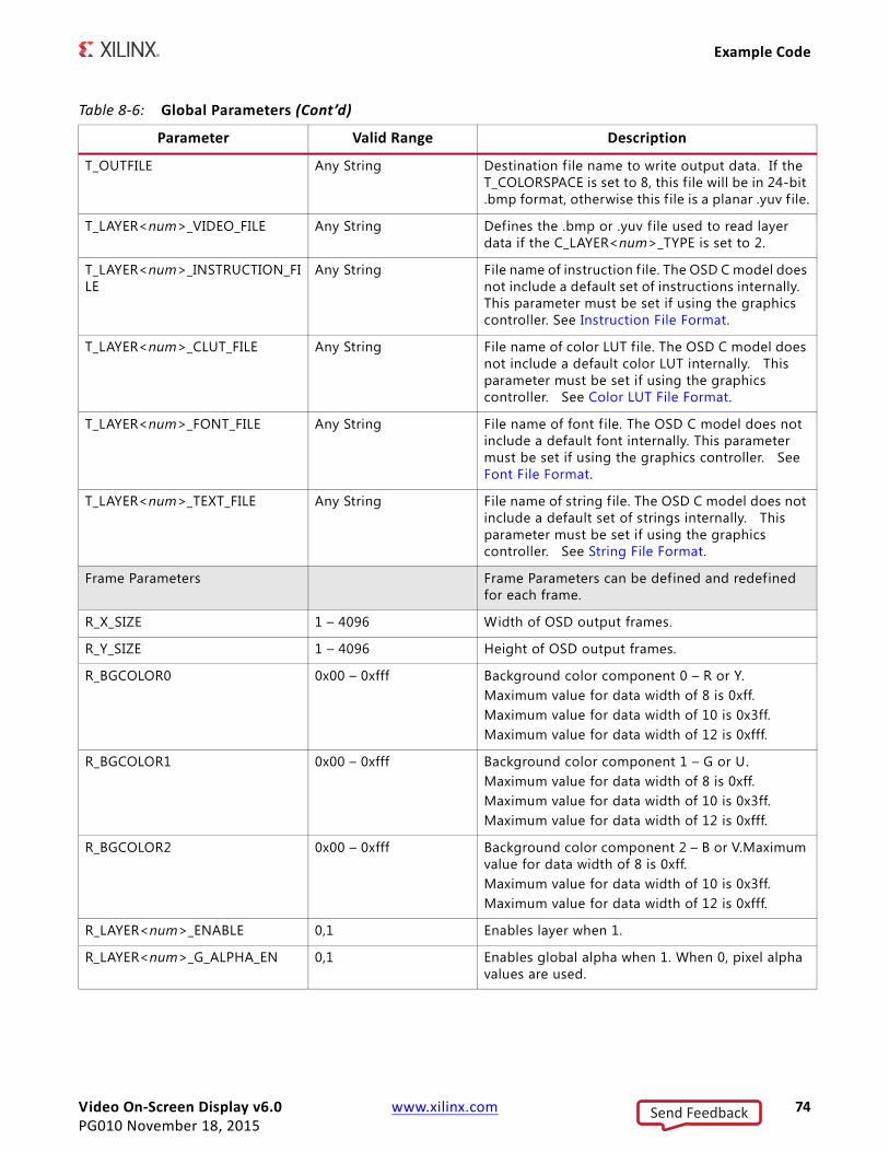
Video On‐Screen Display v6.0 www.xilinx.com 74PG010 November 18, 2015
Example Code
T_OUTFILE Any String Destination f ile name to write output data. If the T_COLORSPACE is set to 8, this f ile will be in 24-bit .bmp format, otherwise this f ile is a planar .yuv f ile.
T_LAYER<num>_VIDEO_FILE Any String Defines the .bmp or .yuv f ile used to read layer data if the C_LAYER<num>_TYPE is set to 2.
T_LAYER<num>_INSTRUCTION_FILE
Any String File name of instruction f ile. The OSD C model does not include a default set of instructions internally. This parameter must be set if using the graphics controller. See Instruction File Format.
T_LAYER<num>_CLUT_FILE Any String File name of color LUT file. The OSD C model does not include a default color LUT internally. This parameter must be set if using the graphics controller. See Color LUT File Format.
T_LAYER<num>_FONT_FILE Any String File name of font f ile. The OSD C model does not include a default font internally. This parameter must be set if using the graphics controller. See Font File Format.
T_LAYER<num>_TEXT_FILE Any String File name of string file. The OSD C model does not include a default set of strings internally. This parameter must be set if using the graphics controller. See String File Format.
Frame Parameters Frame Parameters can be defined and redefined for each frame.
R_X_SIZE 1 – 4096 Width of OSD output frames.
R_Y_SIZE 1 – 4096 Height of OSD output frames.
R_BGCOLOR0 0x00 – 0xfff Background color component 0 – R or Y.Maximum value for data width of 8 is 0xff.Maximum value for data width of 10 is 0x3ff.Maximum value for data width of 12 is 0xfff.
R_BGCOLOR1 0x00 – 0xfff Background color component 1 – G or U.Maximum value for data width of 8 is 0xff.Maximum value for data width of 10 is 0x3ff.Maximum value for data width of 12 is 0xfff.
R_BGCOLOR2 0x00 – 0xfff Background color component 2 – B or V.Maximum value for data width of 8 is 0xff.Maximum value for data width of 10 is 0x3ff.Maximum value for data width of 12 is 0xfff.
R_LAYER<num>_ENABLE 0,1 Enables layer when 1.
R_LAYER<num>_G_ALPHA_EN 0,1 Enables global alpha when 1. When 0, pixel alpha values are used.
Table 8‐6: Global Parameters (Cont’d)
Parameter Valid Range Description
Send Feedback

Video On‐Screen Display v6.0 www.xilinx.com 75PG010 November 18, 2015
Example Code
R_LAYER<num>_PRIORITY 0-7 Z-plane order. Lower values denotes layers that are below layers with higher priority. Each layer must have a unique priority setting.
R_LAYER<num>_ALPHA 0-0xfff Alpha value for 100% opaque to 100% transparent.Maximum value for data width of 8 is 0xff.Maximum value for data width of 10 is 0x3ff.Maximum value for data width of 12 is 0xfff.
R_LAYER<num>_X_POS 0 – (R_X_SIZE-1) X position of upper-left corner of layer.
R_LAYER<num>_Y_POS 0 – (R_Y_SIZE-1) Y position of upper-left corner of layer.
R_LAYER<num>_X_SIZE 0 – R_X_SIZE Width of layer.
R_LAYER<num>_Y_SIZE 0 – R_Y_SIZE Height of layer.
Table 8‐6: Global Parameters (Cont’d)
Parameter Valid Range Description
Send Feedback
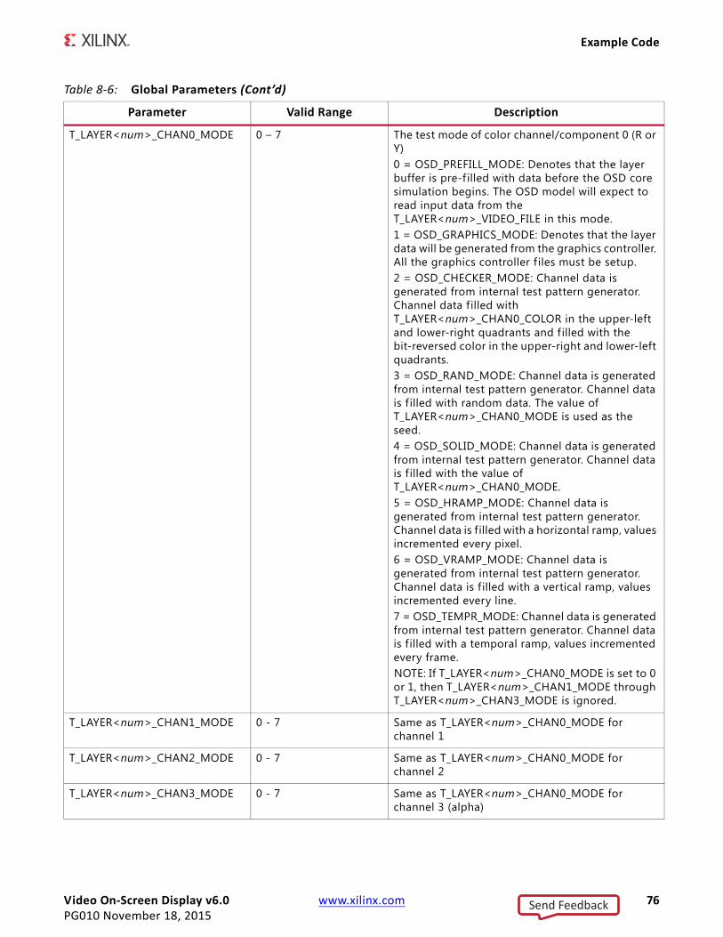
Video On‐Screen Display v6.0 www.xilinx.com 76PG010 November 18, 2015
Example Code
T_LAYER<num>_CHAN0_MODE 0 – 7 The test mode of color channel/component 0 (R or Y)0 = OSD_PREFILL_MODE: Denotes that the layer buffer is pre-f illed with data before the OSD core simulation begins. The OSD model will expect to read input data from the T_LAYER<num>_VIDEO_FILE in this mode.1 = OSD_GRAPHICS_MODE: Denotes that the layer data will be generated from the graphics controller. All the graphics controller f iles must be setup.2 = OSD_CHECKER_MODE: Channel data is generated from internal test pattern generator. Channel data filled with T_LAYER<num>_CHAN0_COLOR in the upper-left and lower-right quadrants and f illed with the bit-reversed color in the upper-right and lower-left quadrants. 3 = OSD_RAND_MODE: Channel data is generated from internal test pattern generator. Channel data is f illed with random data. The value of T_LAYER<num>_CHAN0_MODE is used as the seed.4 = OSD_SOLID_MODE: Channel data is generated from internal test pattern generator. Channel data is f illed with the value of T_LAYER<num>_CHAN0_MODE.5 = OSD_HRAMP_MODE: Channel data is generated from internal test pattern generator. Channel data is f illed with a horizontal ramp, values incremented every pixel.6 = OSD_VRAMP_MODE: Channel data is generated from internal test pattern generator. Channel data is f illed with a vertical ramp, values incremented every line.7 = OSD_TEMPR_MODE: Channel data is generated from internal test pattern generator. Channel data is f illed with a temporal ramp, values incremented every frame.NOTE: If T_LAYER<num>_CHAN0_MODE is set to 0 or 1, then T_LAYER<num>_CHAN1_MODE through T_LAYER<num>_CHAN3_MODE is ignored.
T_LAYER<num>_CHAN1_MODE 0 - 7 Same as T_LAYER<num>_CHAN0_MODE for channel 1
T_LAYER<num>_CHAN2_MODE 0 - 7 Same as T_LAYER<num>_CHAN0_MODE for channel 2
T_LAYER<num>_CHAN3_MODE 0 - 7 Same as T_LAYER<num>_CHAN0_MODE for channel 3 (alpha)
Table 8‐6: Global Parameters (Cont’d)
Parameter Valid Range Description
Send Feedback
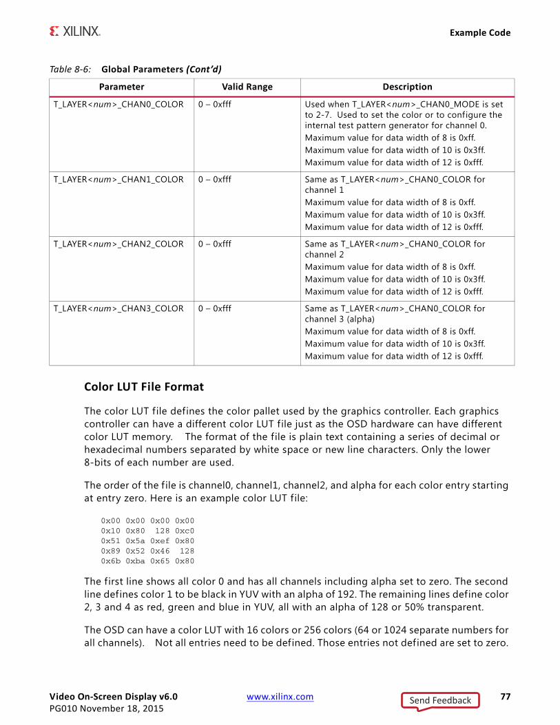
Video On‐Screen Display v6.0 www.xilinx.com 77PG010 November 18, 2015
Example Code
Color LUT File Format
The color LUT file defines the color pallet used by the graphics controller. Each graphics controller can have a different color LUT file just as the OSD hardware can have different color LUT memory. The format of the file is plain text containing a series of decimal or hexadecimal numbers separated by white space or new line characters. Only the lower 8-bits of each number are used.
The order of the f ile is channel0, channel1, channel2, and alpha for each color entry starting at entry zero. Here is an example color LUT file:
0x00 0x00 0x00 0x000x10 0x80 128 0xc00x51 0x5a 0xef 0x800x89 0x52 0x46 1280x6b 0xba 0x65 0x80
The first line shows all color 0 and has all channels including alpha set to zero. The second line defines color 1 to be black in YUV with an alpha of 192. The remaining lines define color 2, 3 and 4 as red, green and blue in YUV, all with an alpha of 128 or 50% transparent.
The OSD can have a color LUT with 16 colors or 256 colors (64 or 1024 separate numbers for all channels). Not all entries need to be defined. Those entries not defined are set to zero.
T_LAYER<num>_CHAN0_COLOR 0 – 0xfff Used when T_LAYER<num>_CHAN0_MODE is set to 2-7. Used to set the color or to configure the internal test pattern generator for channel 0.Maximum value for data width of 8 is 0xff.Maximum value for data width of 10 is 0x3ff.Maximum value for data width of 12 is 0xfff.
T_LAYER<num>_CHAN1_COLOR 0 – 0xfff Same as T_LAYER<num>_CHAN0_COLOR for channel 1Maximum value for data width of 8 is 0xff.Maximum value for data width of 10 is 0x3ff.Maximum value for data width of 12 is 0xfff.
T_LAYER<num>_CHAN2_COLOR 0 – 0xfff Same as T_LAYER<num>_CHAN0_COLOR for channel 2Maximum value for data width of 8 is 0xff.Maximum value for data width of 10 is 0x3ff.Maximum value for data width of 12 is 0xfff.
T_LAYER<num>_CHAN3_COLOR 0 – 0xfff Same as T_LAYER<num>_CHAN0_COLOR for channel 3 (alpha)Maximum value for data width of 8 is 0xff.Maximum value for data width of 10 is 0x3ff.Maximum value for data width of 12 is 0xfff.
Table 8‐6: Global Parameters (Cont’d)
Parameter Valid Range Description
Send Feedback
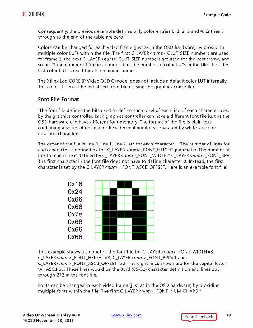
Video On‐Screen Display v6.0 www.xilinx.com 78PG010 November 18, 2015
Example Code
Consequently, the previous example defines only color entries 0, 1, 2, 3 and 4. Entries 5 through to the end of the table are zero.
Colors can be changed for each video frame (just as in the OSD hardware) by providing multiple color LUTs within the file. The first C_LAYER<num>_CLUT_SIZE numbers are used for frame 1, the next C_LAYER<num>_CLUT_SIZE numbers are used for the next frame, and so on. If the number of frames is more than the number of color LUTs in the f ile, then the last color LUT is used for all remaining frames.
The Xilinx LogiCORE IP Video OSD C model does not include a default color LUT internally. The color LUT must be initialized from file if using the graphics controller.
Font File Format
The font f ile defines the bits used to define each pixel of each line of each character used by the graphics controller. Each graphics controller can have a different font f ile just as the OSD hardware can have different font memory. The format of the f ile is plain text containing a series of decimal or hexadecimal numbers separated by white space or new-line characters.
The order of the f ile is line 0, line 1, line 2, etc for each character. The number of lines for each character is defined by the C_LAYER<num>_FONT_HEIGHT parameter. The number of bits for each line is defined by C_LAYER<num>_FONT_WIDTH * C_LAYER<num>_FONT_BPP. The first character in the font file does not have to define character 0. Instead, the f irst character is set by the C_LAYER<num>_FONT_ASCII_OFFSET. Here is an example font file:
This example shows a snippet of the font f ile for C_LAYER<num>_FONT_WIDTH=8, C_LAYER<num>_FONT_HEIGHT=8, C_LAYER<num>_FONT_BPP=1 and C_LAYER<num>_FONT_ASCII_OFFSET=32. The eight lines shown are for the capital letter 'A', ASCII 65. These lines would be the 33rd (65-32) character definition and lines 265 through 272 in the font f ile.
Fonts can be changed in each video frame (just as in the OSD hardware) by providing multiple fonts within the f ile. The f irst C_LAYER<num>_FONT_NUM_CHARS *
Send Feedback

Video On‐Screen Display v6.0 www.xilinx.com 79PG010 November 18, 2015
Example Code
C_LAYER<num>_FONT_WIDTH * C_LAYER<num>_FONT_HEIGHT numbers are used for frame 1, the next C_LAYER<num>_FONT_NUM_CHARS *C_LAYER<num>_FONT_WIDTH * C_LAYER<num>_FONT_HEIGHT numbers are used for the next frame, andso on. If the number of frames is more than the number of fonts in the f ile, then the last font is used for all remaining frames.
The Xilinx LogiCORE IP Video OSD C model does not include a default font internally. The font must be initialized from a file if using the graphics controller.
String File Format
The string file defines the text strings used by the graphics controller. Each graphics controller can have a different font file just as the OSD hardware can have different font memory. The format of the file is plain text containing one string of characters including spaces per line.
The order of the f ile is string 0, string 1, string 2, and so on, again, one string per line. The number of strings for each graphics controller is defined by this parameter:
C_LAYER<num>_TEXT_NUM_STRINGS
The maximum number of characters (including the terminating NULL character) is defined by this parameter:
C_LAYER<num>_TEXT_MAX_STRING_LENGTH parameter
Here is an example string file:
This is String # 0. It is on one line! String 1XilinxOSDMenu!&^%!@#*
In the previous example f ile, only the f irst lines (up to C_LAYER<num>_TEXT_NUM _STRINGS number of lines) are used. All other lines are ignored. Also, the f irst characters of each line (up to C_LAYER<num>_TEXT_MAX_STRING_LENGTH) are used. All other characters are ignored. If the maximum string length was set to 8, the first string would be truncated to “This is\0”.
Note: In the OSD hardware, any character after the f irst NULL character in a string is ignored and not displayed.
Strings can be changed in each video frame by providing multiple sets of strings within the string f ile. The f irst C_LAYER<num>_TEXT_NUM_STRINGS number of lines are used for frame 1, the next C_LAYER<num>_TEXT_NUM_STRINGS number of lines are used for the next frame, and so on. If the number of frames is more than the number of sets of strings in the file, then the last set of strings are used for all remaining frames.
Send Feedback

Video On‐Screen Display v6.0 www.xilinx.com 80PG010 November 18, 2015
Example Code
The Xilinx LogiCORE IP Video OSD C model does not include a default set of strings internally. The text strings must be initialized from a file if using the graphics controller.
Instruction File Format
The instruction f ile defines the instructions used by the graphics controller. Each graphics controller can have a different instruction f ile just as the OSD hardware can have different instruction memory. The format of the f ile is plain text containing one string of characters including spaces per line. One full instruction is contained on each line.
The order of the f ile is instruction, x_start, x_stop, y_start, y_stop, color_index, text_index and object_size on each line. The instruction field is a text string describing the graphics instruction. All other f ields are either decimal or hexadecimal numbers for the parameters of the instruction.
Here is an example instruction file:
############################ Frame 1 Instructions###########################BOX 10 20 40 80 1 0 4BOX 40 60 70 90 3 0 4TEXT 100 100 50 50 2 1 0x40BOXTEXT 30 40 30 40 2 2 0x14END############################ Frame 2 Instructions###########################TEXT 100 100 50 50 2 1 0x40BOX 20 40 40 80 1 0 4BOX 40 80 70 90 3 0 4TEXT 200 100 50 50 2 1 0x40BOXTEXT 30 40 30 40 2 2 0x14END
Each f ield is described in Table 8-7.
Table 8‐7: Instruction File Fields
Field Valid Range Description
Instruction BOX, TEXT, BOXTEXT, END The graphics instruction.
Xstart 0 – end of line Starting draw x position of the instruction.
Xstop 0 – end of line Ending draw x position of the instruction.
Ystart 0 – end of frame Starting draw y position of the instruction.
Ystop 0 – end of frame Ending draw y position of the instruction.
Send Feedback

Video On‐Screen Display v6.0 www.xilinx.com 81PG010 November 18, 2015
Example Code
See Instruction RAM in Appendix D for more information on the format of each instruction.
There are two “END”s in the example instruction f ile because the f ile is used to describe the instructions for each video frame. All instructions from the beginning of the f ile to the f irst END are displayed on frame 1. For each frame following, the instructions between each subsequent “END” are displayed. If the number of frames is more than the number of “END”s in the f ile, then the last set of instructions are displayed for all remaining frames.
The Xilinx LogiCORE IP Video OSD C model does not include a default set of instructions internally. The instructions must be initialized from a f ile if using the graphics controller.
Initializing the OSD Input Video Structure
The easiest way to assign stimuli values to the input video structure is to initialize it with an image or video. The bmp_util.h, yuv_utils.h, rgb_utils.h and video_util.h header f iles packaged with the bit accurate C models contain functions to facilitate file I/O.
Bitmap Image Files
The rgb_utils.h and bmp_utils.h f iles declare functions that help access files in Windows bitmap format (http://en.wikipedia.org/wiki/BMP_file_format). However, this format limits color depth to a maximum of 8 bits per pixel, and operates on images with three planes (R,G,B). Consequently, the following functions operate on arguments type rgb8_video_struct, which is defined in rgb_utils.h. Also, both functions support only true color, non-indexed formats with 24 bits per pixel.
int write_bmp(FILE *outfile, struct rgb8_video_struct *rgb8_video);int read_bmp(FILE *infile, struct rgb8_video_struct *rgb8_video);
These functions are used to dynamically allocate and free memory for RGB structure storage:
int alloc_rgb8_frame_buff(struct rgb8_video_struct* rgb8video );
Color index 0 – 15 or 255 The color to be used for the graphics object. For boxes, this color index is used directly.For Text with BPP=1, the color index is used for the background and the color index + 1 is used for the foreground.For Text with BPP=2, the color index is used for bits “00” in the font, color index + 1 for bits “01”, color index + 2 for “10” and color index + 3 for “11”.
Text index 0 – (number of strings -1) The text string to draw.
Object Size 0 – 0xff For BOX, Size of boxes.For BOXTEXT, [3:0] size of boxes, [7;4] size of text.For TEXT, bits [7:4] size of text.
Table 8‐7: Instruction File Fields (Cont’d)
Send Feedback
Video On‐Screen Display v6.0 www.xilinx.com 82PG010 November 18, 2015
Example Code
void free_rgb_frame_buff(struct rgb_video_struct* rgb_video );
Exchanging data between rgb8_video_struct and general video_struct type frames/videos is facilitated by functions:
int copy_rgb8_to_video(struct rgb8_video_struct* rgb8_in, struct video_struct* video_out ); int copy_video_to_rgb8( struct video_struct* video_in, struct rgb8_video_struct* rgb8_out );
Note: All image / video manipulation utility functions expect both input and output structures initialized; for example, pointing to a structure that has been allocated in memory, either as static or dynamic variables. Additionally, the input structure must have the dynamically allocated containers (data, r, g, b, y, u, and v arrays) already allocated and initialized with the input frame(s). If the output container structure is pre-allocated at the time of the function call, the utility functions verify and issue an error if the output container size does not match the size of the expected output. If the output container structure is not pre-allocated, the utility functions create the appropriate container to hold results.
YUV Image/Video Files
The yuv_utils.h f ile declares functions that support f ile access in YUV format. These functions are used to dynamically allocate and free memory for YUV structure storage:
int alloc_yuv8_frame_buff(struct yuv8_video_struct* yuv8video );void free_yuv_frame_buff(struct yuv_video_struct* yuv_video );
These functions allow reading and writing of YUV functions (used to initialize or write yuv8_video data):
int write_yuv(FILE *outfile, struct yuv8_video_struct *yuv8_video);int read_yuv(FILE *infile, struct yuv8_video_struct *yuv8_video);
Exchanging data between yuv8_video_struct and general video_struct type frames/videos is facilitated by functions:
int copy_yuv8_to_video(struct yuv8_video_struct* yuv8_in, struct video_struct* video_out ); int copy_video_to_yuv8( struct video_struct* video_in, struct yuv8_video_struct* yuv8_out );
YUV formats (4:2:0, 4:2:2 and 4:4:4) can be converted with these functions:
int yuv8_420to444(struct yuv8_video_struct* video_in, struct yuv8_video_struct* video_out);int yuv8_422to444(struct yuv8_video_struct* video_in, struct yuv8_video_struct* video_out);int yuv8_444to420(struct yuv8_video_struct* video_in, struct yuv8_video_struct* video_out);int yuv8_444to422(struct yuv8_video_struct* video_in, struct yuv8_video_struct* video_out);
Binary Image/Video Files
The video_utils.h f ile declares functions that help load and save generalized video f iles in raw, uncompressed format. These functions effectively serialize the video_struct structure:
Send Feedback

Video On‐Screen Display v6.0 www.xilinx.com 83PG010 November 18, 2015
Example Code
int read_video( FILE* infile, struct video_struct* in_video);int write_video(FILE* outfile, struct video_struct* out_video);
The corresponding file contains a small, plain text header defining, “Mode”, “Frames”, “Rows”, “Columns”, and “Bits per Pixel”. The plain text header is followed by binary data, 16-bits per component in scan line continuous format. Subsequent frames contain as many component planes as defined by the video mode value selected. Also, the size (rows, columns) of component planes can differ within each frame as defined by the actual video mode selected.
These functions are used to dynamically allocate and free memory for video structure storage:
int alloc_video_buff(struct video_struct* video );void free_video_buff(struct video_struct* video );
Compiling on 32‐bit and 64‐bit Windows Platforms
Precompiled library v_osd_v6_0_bitacc_cmodel.lib, top level demonstration code run_bitacc_cmodel_config.c and example code run_bitacc_cmodel.c must be compiled with an ANSI C compliant compiler under Windows 32-bit or Windows 64-bit. This section describes an example using Microsoft Visual Studio.
In Visual Studio create a new, empty Win32 Console Application project. As existing items, add:
• libIpv_osd_v6_0_bitacc_cmodel.lib to the “Resource Files” folder of the project
• run_bitacc_cmodel.c or the run_bitacc_cmodel_config.c to the “Source Files” folder of the project
• v_osd_v6_0_bitacc_cmodel.h header file to the “Header Files” folder of the project
• bmp_utils.h f ile to the “Header Files” folder of the project
• rgb_utils.h f ile to the “Header Files” folder of the project
• video_fio.h f ile to the “Header Files” folder of the project
• video_utils.h f ile to the “Header Files” folder of the project
• yuv_utils.h f ile to the “Header Files” folder of the project
To build the x64 executable for 64-bit Windows platforms, perform these steps. These steps can be skipped if building the Win32 executable.
1. Right-click on the solution in the Solution Explorer and click Properties at the bottom of the pop-up menu.
2. Click Configuration Manager.
Send Feedback

Video On‐Screen Display v6.0 www.xilinx.com 84PG010 November 18, 2015
Example Code
3. In the Active solution platform drop-down box, select <New…>.
4. In the new platform drop-down box, select x64 and click OK.
Make sure that all the projects now have x64 as the default platform in the Configuration Manager.
5. After the project is created and populated, it must be compiled and linked (built) to create a Win32 or x64 executable. To perform the build step, select Build Solution from the Build menu. An executable matching the project name is created either in the Debug or Release subdirectories under the project location based on whether “Debug” or “Release” has been selected in the “Configuration Manager” under the Build menu.
Note: The run_bitacc_cmodel.c f ile is an example demonstration that reads no input but generates an output .yuv f ile from internally generated test patterns. The run_bitacc_cmodel_config.c f ile is a configurable demonstration and requires several input f iles to run. See Running the Executables for information on command line arguments and input f ile formats.
Compiling under 32‐bit and 64‐bit Linux Platforms
Example Demonstration
To compile the example demonstration, go to the directory where the header files, the library f iles and run_bitacc_cmodel.c were unpacked. The libraries and header files are referenced during the compilation and linking process. In this directory, perform these steps:
1. Set your LD_LIBRARY_PATH environment variable to include the root directory where the model zip f ile was unzipped. For example:
setenv LD_LIBRARY_PATH <unzipped_c_model_dir>:${LD_LIBRARY_PATH}
2. Copy these files from the /lin32 or /lin64 directory to the root directory:
libIp_v_osd_v6_0_bitacc_cmodel.so libIp_v_tc_v6_0_bitacc_cmodel.so
3. In the root directory, compile using the GNU C Compiler by typing this command at the shell prompt:
gcc -m32 -x c++ ../run_bitacc_cmodel.c ../parsers.c -o run_bitacc_cmodel -L. -lIp_v_osd_v6_0_bitacc_cmodel -Wl,-rpath,.
gcc –m64 -x c++ ../run_bitacc_cmodel.c ../parsers.c -o run_bitacc_cmodel -L. -lIp_v_osd_v6_0_bitacc_cmodel -Wl,-rpath,.
4. This results in the creation of the executable run_bitacc_cmodel, which can be run using this command:
./run_bitacc_cmodel
Send Feedback

Video On‐Screen Display v6.0 www.xilinx.com 85PG010 November 18, 2015
Example Code
A make f ile is also included that runs GCC. To clean the executable and compile the example code, enter this command at the shell prompt:
make clean all
Configurable Demonstration
To compile the configurable demonstration, go to the directory where the header files, the library f iles and run_bitacc_cmodel_config.c were unpacked. The libraries and header f iles are referenced during the compilation and linking process. In this directory, perform these steps:
1. Set your LD_LIBRARY_PATH environment variable to include the root directory where the model zip-file was unzipped. For example:
setenv LD_LIBRARY_PATH <unzipped_c_model_dir>:${LD_LIBRARY_PATH}
2. Copy these files from the /lin64 directory to the root directory:
libIp_v_osd_v6_0_bitacc_cmodel.so libIp_v_tc_v6_0_bitacc_cmodel.so
3. In the root directory, compile using the GNU C Compiler by entering this command at the shell prompt:
gcc -x c++ run_bitacc_cmodel_config.c -o run_bitacc_cmodel_config -L. -lIp_v_osd_v6_0_bitacc_cmodel -Wl,-rpath,.
4. This results in the creation of the executable run_bitacc_cmodel, which can be run using this command:
./run_bitacc_cmodel_config –c <Config Filename> <-parameter=value ...>
A make f ile is also included that runs GCC. To clean the executable and compile the example code, enter this following command at the shell prompt:
make clean run_bitacc_cmodel_config
Running the Executables
Included in the zip f ile are precompiled executable f iles for use with 32-bit and 64-bit Windows and Linux platforms. The instructions for running on each platform are included in this section.
Example Demonstration
The example demonstration does not use command line parameters. To run on a 32-bit or 64-bit Linux platform, perform these steps:
1. Set your $LD_LIBRARY_PATH environment variable to include the root directory where the model zip file was unzipped. For example:
Send Feedback
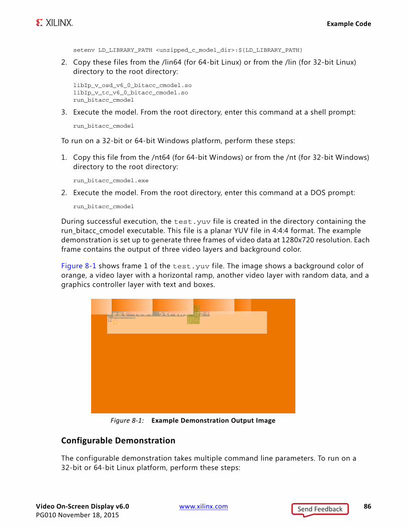
Video On‐Screen Display v6.0 www.xilinx.com 86PG010 November 18, 2015
Example Code
setenv LD_LIBRARY_PATH <unzipped_c_model_dir>:${LD_LIBRARY_PATH}
2. Copy these files from the /lin64 (for 64-bit Linux) or from the /lin (for 32-bit Linux) directory to the root directory:
libIp_v_osd_v6_0_bitacc_cmodel.so libIp_v_tc_v6_0_bitacc_cmodel.sorun_bitacc_cmodel
3. Execute the model. From the root directory, enter this command at a shell prompt:
run_bitacc_cmodel
To run on a 32-bit or 64-bit Windows platform, perform these steps:
1. Copy this f ile from the /nt64 (for 64-bit Windows) or from the /nt (for 32-bit Windows) directory to the root directory:
run_bitacc_cmodel.exe
2. Execute the model. From the root directory, enter this command at a DOS prompt:
run_bitacc_cmodel
During successful execution, the test.yuv f ile is created in the directory containing the run_bitacc_cmodel executable. This f ile is a planar YUV file in 4:4:4 format. The example demonstration is set up to generate three frames of video data at 1280x720 resolution. Each frame contains the output of three video layers and background color.
Figure 8-1 shows frame 1 of the test.yuv f ile. The image shows a background color of orange, a video layer with a horizontal ramp, another video layer with random data, and a graphics controller layer with text and boxes.
Configurable Demonstration
The configurable demonstration takes multiple command line parameters. To run on a32-bit or 64-bit Linux platform, perform these steps:
X-Ref Target - Figure 8-1
Figure 8‐1: Example Demonstration Output Image
Send Feedback

Video On‐Screen Display v6.0 www.xilinx.com 87PG010 November 18, 2015
Example Code
1. Set your $LD_LIBRARY_PATH environment variable to include the root directory where the model zip-file was unzipped. For example:
setenv LD_LIBRARY_PATH <unzipped_c_model_dir>:${LD_LIBRARY_PATH}
2. Copy these files from the /lin64 (for 64-bit Linux) or from the /lin (for 32-bit Linux) directory to the root directory:
libIp_v_osd_v6_0_bitacc_cmodel.so libIp_v_tc_v6_0_bitacc_cmodel.so
run_bitacc_cmodel_config
3. Execute the model. From the root directory, enter this command at a shell prompt:
run_bitacc_cmodel_config –c <Config Filename> <-parameter=value …>
Send Feedback

Video On‐Screen Display v6.0 www.xilinx.com 88PG010 November 18, 2015
Example Code
To run on a 32-bit or 64-bit Windows platform, perform these steps:
1. Copy this f ile from the /nt64 (for 64-bit Windows) or from the /nt (for 32-bit Windows) directory to the root directory:
run_bitacc_cmodel_config.exe
2. Execute the model. From the root directory, enter this command at a DOS prompt:
run_bitacc_cmodel_config –c <Config Filename> <-parameter=value …>
The configurable demonstration reads parameters from the config f ile specif ied with the-i <config_file> argument where <config_file> is the relative path and f ilename of the config file. See Config File Format for more information. Parameters in the config f ile can be overridden on the command line by prefixing the parameter with a dash ('-') and removing white spaces. For example, the number of frames to simulate can be overridden with this command line argument "-T_NUM_FRAMES=2". Config parameters set on the command line must be set after the -i argument to take effect.
Figure 8-2 shows frame 1 of the output of the configurable demonstration from this command line:
run_bitacc_cmodel_config –c examples/example0.cfg
The image shows a background color of green, a video layer with a horizontal ramp and another video layer with random data.X-Ref Target - Figure 8-2
Figure 8‐2: Configurable Demonstration Output Image (Example 0)
Send Feedback

Video On‐Screen Display v6.0 www.xilinx.com 89PG010 November 18, 2015
Example Code
Figure 8-3 shows frame 1 of the output of the configurable demonstration from this command line:
run_bitacc_cmodel_config –c examples/example1.cfg
The image shows a background color of grey, a video layer with a horizontal ramp and another video layer with a vertical ramp. Each ramp layer (vertical and horizontal) have different ramp starting values for each color component.
Figure 8-4 shows frame 1 of the output of the configurable demonstration from this command line:
run_bitacc_cmodel_config –c examples/example2.cfg
X-Ref Target - Figure 8-3
Figure 8‐3: Configurable Demonstration Output Image (Example 1)
Send Feedback

Video On‐Screen Display v6.0 www.xilinx.com 90PG010 November 18, 2015
Example Code
The image shows a background color of red, a video layer from a BMP file input and another video layer with random data.X-Ref Target - Figure 8-4
Figure 8‐4: Configurable Demonstration Output Image (Example 2)
Send Feedback

Video On‐Screen Display v6.0 www.xilinx.com 91PG010 November 18, 2015
Example Code
Figure 8-5 shows frame 1 of the output of the configurable demonstration from this command line:
run_bitacc_cmodel_config –c examples/example3.cfg
The image shows a background color of grey, a video layer from a BMP file input, six other video layers with checkerboard, horizontal ramp and vertical ramp patterns. One graphics controller layer is also displayed generating multi-colored lines, boxes and text.X-Ref Target - Figure 8-5
Figure 8‐5: Configurable Demonstration Output Image (Example 3)
Send Feedback

Video On‐Screen Display v6.0 www.xilinx.com 92PG010 November 18, 2015
Chapter 9
Test BenchThis chapter contains information about the provided test bench in the Vivado® Design Suite environment.
Demonstration Test BenchA demonstration test bench is provided with the core which enables you to observe core behavior in a typical scenario. This test bench is generated together with the core in Vivado Design Suite. You are encouraged to make simple modif ications to the configurations and observe the changes in the waveform.
Directory and File Contents
The following files are expected to be generated in the in the demonstration test bench output directory:
• axi4lite_mst.v
• axi4s_video_mst.v
• axi4s_video_slv.v
• ce_generator.v
• tb_<IP_instance_name>.v
Test Bench Structure
The top-level entity is tb_<IP_instance_name>.
It instantiates the following modules:
• DUT
The <IP> core instance under test.
• axi4lite_mst
Send Feedback
Video On‐Screen Display v6.0 www.xilinx.com 93PG010 November 18, 2015
Chapter 9: Test Bench
The AXI4-Lite master module, which initiates AXI4-Lite transactions to program core registers.
• axi4s_video_mst
The AXI4-Stream master module, which generates ramp data and initiates AXI4-Stream transactions to provide video stimuli for the core and can also be used to open stimuli f iles generated from the reference C models and convert them into corresponding AXI4-Stream transactions.
To do this, edit tb_<IP_instance_name>.v:
a. Add define macro for the stimuli f ile name and directory pathdefine STIMULI_FILE_NAME<path><filename>.
b. Comment-out/remove the following line:MST.is_ramp_gen(`C_ACTIVE_ROWS, `C_ACTIVE_COLS, 2);and replace with the following line:MST.use_file(`STIMULI_FILE_NAME);
For information on how to generate stimuli f iles, see Chapter 4, C Model Reference.
• axi4s_video_slv
The AXI4-Stream slave module, which acts as a passive slave to provide handshake signals for the AXI4-Stream transactions from the core output, can be used to open the data files generated from the reference C model and verify the output from the core.
To do this, edit tb_<IP_instance_name>.v:
a. Add define macro for the golden f ile name and directory pathdefine GOLDEN_FILE_NAME “<path><filename>”.
b. Comment out the following line:SLV.is_passive;and replace with the following line:SLV.use_file(`GOLDEN_FILE_NAME);
For information on how to generate golden f iles, see Chapter 4, C Model Reference.
• ce_gen
Programmable Clock Enable (ACLKEN) generator.
Send Feedback

Video On‐Screen Display v6.0 www.xilinx.com 94PG010 November 18, 2015
Appendix A
Verification, Compliance, and Interoperability
This appendix includes information about how the IP was tested for compliance with the protocol to which it was designed.
SimulationA highly parameterizable test bench was used to test the Video On-Screen Display core. Testing included the following:
• Register accesses
• Processing of multiple frames of data
• Testing of various frame sizes including 1080p, 720p and 480p
• Varying instantiations of the core
• Varying the data width including 8, 10 and 12
• Varying the number of data channels including 2 and 3
• Varying the number and type of layers including AXI4-Stream input interfaces and Graphics controllers
• Varying size, location, transparency and over/under of video layers
• Varying the background color
• Varying the number, size, color and transparency of boxes, text generated from the internal graphics controller
Hardware TestingThe Video On-Screen Display core has been tested in a variety of hardware platforms at Xilinx to represent a variety of parameterizations, including the following:
Send Feedback

Video On‐Screen Display v6.0 www.xilinx.com 95PG010 November 18, 2015
Interoperability
• A test design was developed for the core that incorporated a MicroBlaze™ processor, AXI4 Interconnect and various other peripherals. The software for the test system included live video input and output for the Video On-Screen Display core. Various tests could be supported by varying the configuration of the Video On-Screen Display core or by loading a different software executable. The MicroBlaze processor was responsible for:
° Initializing the appropriate input and output buffers in external memory
° Initializing the Video On-Screen Display core
° Initializing the HDMI/DVI input and output cores for live video
° Launching the test
° Configuring the Video On-Screen Display for various input frame sizes, positions and transparency
° Launching various graphics controller tests for box and text placement, color, size and transparency
° Launching OSD demos including video/graphics resize/movement and on-screen menu demos
° Controlling the peripherals including the UART and AXI VDMAs
InteroperabilityThe core slave (input) AXI4-Stream interface can work directly with any Video core which produces RGB, YCrCb 4:4:4, YCrCb 4:2:2, or YCrCb 4:2:0 data. The core master (output) RGB interface can work directly with any Video core which consumes RGB, YCrCb 4:4:4, YCrCb 4:2:2, or YCrCb 4:2:0 data.
Send Feedback

Video On‐Screen Display v6.0 www.xilinx.com 96PG010 November 18, 2015
Appendix B
Migrating and UpgradingThis appendix contains information about migrating from an ISE design to the Vivado Design Suite, and for upgrading to a more recent version of the IP core. For customers upgrading their IP core, important details (where applicable) about any port changes and other impact to user logic are included.
Migrating to the Vivado Design SuiteFor information about migration to Vivado Design Suite, see ISE to Vivado Design Suite Migration Guide (UG911) [Ref 2].
Upgrading in Vivado Design SuiteThis section provides information about any changes to the user logic or port designations that take place when you upgrade to a more current version of this IP core in the Vivado Design Suite.
Parameter Changes
There are no parameter changes.
Port Changes
The Video On-Screen Display v5.01.a removed all TKEEP ports form the AXI4-Stream interfaces.
TUSER ports were added to the AXI4-Stream interfaces.
All XSVI ports were removed.
The IP2INTC_Irpt output port was renamed to IRQ.
The INTC_IF output bus was added.
Send Feedback

Video On‐Screen Display v6.0 www.xilinx.com 97PG010 November 18, 2015
Upgrading in Vivado Design Suite
The Video On-Screen Display v3.0 changed the port widths of all VFBC interfaces, and added the video_data_in input port.
Other Changes
Migrating to the AXI4‐Lite Interface
The Video On-Screen Display v3.0 changed from the PLB processor interface to the AXI4-Lite interface. As a result, all of the PLB-related connections have been replaced with an AXI4-Lite interface. For more information, see:
http://Xilinx Support web page/documentation/ip_documentation/ug761_axi_reference_guide.pdf
Migrating to the AXI4‐Stream Interface
The Video On-Screen Display v5.01.a removed all XSVI inputs and outputs, replacing the functionality with AXI4-Stream interfaces. For more information bridging the XSVI and AXI4-Stream interfaces, see:
http://www.xilinx.com/support/documentation/application_notes/xapp521_XSVI_AXI4.pdf
The Video On-Screen Display v3.0 changed from the Video Frame Buffer Controller (VFBC) native interfaces to the AXI4-Stream interfaces. As a result, all of the VFBC-related connections have been replaced with an AXI4-Lite interface. For more information, see:
http://www.xilinx.com/support/documentation/ip_documentation/ug761_axi_reference_guide.pdf
Functionality Changes
The Video On-Screen Display v3.0 added the ability to drive the video output from one XSVI input video source. This allows overlaying graphics (from Internal Graphics Controller) from live streaming video without the use of external memory. The option to select an XSVI output has been removed in v5.01.a. If live video out is needed, then the user can use the AXI4-Stream to Video Out or AXI4-Stream to XSVI, using components from XAPP521 (v1.0), Bridging Xilinx Streaming Video Interface with the AXI4-Stream Protocol located at:
http://www.xilinx.com/support/documentation/application_notes/xapp521_XSVI_AXI4.pdf.
Send Feedback

Video On‐Screen Display v6.0 www.xilinx.com 98PG010 November 18, 2015
Appendix C
DebuggingThis appendix includes details about resources available on the Xilinx Support website and debugging tools.
Finding Help on Xilinx.comTo help in the design and debug process when using the On-Screen Display, the Xilinx Support web page (Xilinx Support web page) contains key resources such as product documentation, release notes, answer records, information about known issues, and links for opening a Technical Support Web Case.
Documentation
This product guide is the main document associated with the On-Screen Display. This guide, along with documentation related to all products that aid in the design process, can be found on the Xilinx Support web page or by using the Xilinx Documentation Navigator.
Download the Xilinx Documentation Navigator from the Downloads page. For more information about this tool and the features available, open the online help after installation.
Answer Records
Answer Records include information about commonly encountered problems, helpful information on how to resolve these problems, and any known issues with a Xilinx product. Answer Records are created and maintained daily ensuring that users have access to the most accurate information available.
Answer Records for this core are listed below, and can also be located by using the Search Support box on the main Xilinx support web page. To maximize your search results, use proper keywords such as
• Product name
• Tool message(s)
• Summary of the issue encountered
Send Feedback

Video On‐Screen Display v6.0 www.xilinx.com 99PG010 November 18, 2015
Appendix C: Debugging
A filter search is available after results are returned to further target the results.
Answer Records for the On-Screen Display Core
AR 54539http://www.xilinx.com/support/answers/54539.htm
Technical Support
Xilinx provides technical support in the Xilinx Support web page for this LogiCORE™ IP product when used as described in the product documentation. Xilinx cannot guarantee timing, functionality, or support if you do any of the following:
• Implement the solution in devices that are not defined in the documentation.
• Customize the solution beyond that allowed in the product documentation.
• Change any section of the design labeled DO NOT MODIFY.
Xilinx provides premier technical support for customers encountering issues that require additional assistance.
To contact Xilinx Technical Support, navigate to the Xilinx Support web page.
1. Open a WebCase by selecting the WebCase link located under Support Quick Links.
• A block diagram of the video system that explains the video source, destination and IP (custom and Xilinx) used.
Note: Access to WebCase is not available in all cases. Please login to the WebCase tool to see your specif ic support options.
Debug ToolsThere are many tools available to address On-Screen Display design issues. It is important to know which tools are useful for debugging various situations.
Example Design
The Video On-Screen Display is delivered with an example test bench. Information about the example test bench can be found in Chapter 6, Example Design for the Vivado™ Design Suite.
Vivado Design Suite Debug Feature
Vivado inserts logic analyzer and virtual I/O cores directly into your design. Vivado Lab Tools allows you to set trigger conditions to capture application and integrated block port
Send Feedback

Video On‐Screen Display v6.0 www.xilinx.com 100PG010 November 18, 2015
Appendix C: Debugging
signals in hardware. Captured signals can then be analyzed. This feature represents the functionality in the Vivado IDE that is used for logic debugging and validation of a design running in Xilinx FPGA devices in hardware.
The Vivado logic analyzer is used to interact with the logic debug LogiCORE IP cores, including:
• ILA 2.0 (and later versions)
• VIO 2.0 (and later versions)
Reference Boards
Various Xilinx development boards support On-Screen Display. These boards can be used to prototype designs and establish that the core can communicate with the system.
• 7 series evaluation boards
° KC705
° ZC702
C‐Model Reference
Please see C Model Reference in Chapter 8 in this guide for tips and instructions for using the provided C Model f iles to debug your design.
License Checkers
If the IP requires a license key, the key must be verif ied. The Vivado tool flows have a number of license check points for gating licensed IP through the flow. If the license check succeeds, the IP may continue generation. Otherwise, generation halts with error. License checkpoints are enforced by the following tools:
• Vivado flow: RDS, RDI, Bitgen
IMPORTANT: IP license level is ignored at checkpoints. The test confirms a valid license exists. It does not check IP license level.
Hardware DebugHardware issues can range from link bring-up to problems seen after hours of testing. This section provides debug steps for common issues. The Vivado Lab Tools are a valuable resource to use in hardware debug. The signal names mentioned in the following individual sections can be probed using the Vivado Lab Tools for debugging the specif ic problems.
Send Feedback
Video On‐Screen Display v6.0 www.xilinx.com 101PG010 November 18, 2015
Appendix C: Debugging
Many of these common issues can also be applied to debugging design simulations. Details are provided on General Checks
General Checks
Ensure that all the timing constraints for the core were properly incorporated from the example design and that all constraints were met during implementation.
• Does it work in post-place and route timing simulation? If problems are seen in hardware but not in timing simulation, this could indicate a PCB issue. Ensure that all clock sources are active and clean.
• If using MMCMs in the design, ensure that all MMCMs have obtained lock by monitoring the LOCKED port.
• If your outputs go to 0, check your licensing. The evaluation version of the core will time out after running for 8 hours at 75 MHz.
Evaluation Core Timeout
The On-Screen Display hardware evaluation core times out after approximately eight hours of operation. The output is driven to zero. This results in a black screen for RGB color systems and in a dark-green screen for YUV color systems.
Interface Debug
AXI4‐Lite Interfaces
Table C-1 describes how to troubleshoot the AXI4-Lite interface.
Table C‐1: Troubleshooting the AXI4‐Lite Interface
Symptom Solution
Readback from the Version Register via the AXI4-Lite interface times out, or a core instance without an AXI4-Lite interface seems non-responsive.
Are the S_AXI_ACLK and ACLK pins connected?The VERSION_REGISTER readout issue may be indicative of the core not receiving the AXI4-Lite interface.
Readback from the Version Register via the AXI4-Lite interface times out, or a core instance without an AXI4-Lite interface seems non-responsive.
Is the core enabled? Is s_axi_aclken connected to vcc? Verify that signal ACLKEN is connected to either net_vcc or to a designated clock enable signal.
Send Feedback

Video On‐Screen Display v6.0 www.xilinx.com 102PG010 November 18, 2015
Appendix C: Debugging
Assuming the AXI4-Lite interface works, the second step is to bring up the AXI4-Stream interfaces.
AXI4‐Stream Interfaces
Table C-2 describes how to troubleshoot the AXI4-Stream interface.
Readback from the Version Register via the AXI4-Lite interface times out, or a core instance without an AXI4-Lite interface seems non-responsive.
Is the core in reset? S_AXI_ARESETn and ARESETn should be connected to vcc for the core not to be in reset. Verify that the S_AXI_ARESETn and ARESETn signals are connected to either net_vcc or to a designated reset signal.
Readback value for the VERSION_REGISTER is different from expected default values
The core and/or the driver in a legacy SDK project has not been updated. Ensure that old core versions, implementation f iles, and implementation caches have been cleared.
Table C‐2: Troubleshooting AXI4‐Stream Interface
Symptom Solution
Bit 0,4,8,12,16,20,24,28 of the ERROR register reads back set.
These bits of the ERROR register, EOL_EARLY, indicates the number of pixels received between the latest and the preceding End-Of-Line (EOL) signal for the given AXI4-Stream Slave/Layer was less than the value programmed into the OSD Layer # Size registers. If the values were provided by the Video Timing Controller core, read out ACTIVE_SIZE register value from the VTC core again, and make sure that the TIMING_LOCKED flag is set in the VTC core. Otherwise, measure the number of active AXI4-Stream transactions between EOL pulses.
Bit 1,5,9,13,17,21,25,29 of the ERROR register reads back set.
These bits of the ERROR register, EOL_LATE, indicates the number of pixels received between the last End-Of-Line (EOL) signal for the given AXI4-Stream Slave/Layer surpassed the value programmed into the OSD Layer # Size register. If the values were provided by the Video Timing Controller core, read out ACTIVE_SIZE register value from the VTC core again, and make sure that the TIMING_LOCKED flag is set in the VTC core. Otherwise, measure the number of active AXI4-Stream transactions between EOL pulses.
Bit 2,6,10,14,18,22,26,30 or Bit 3,7,11,15,19,23,27,31 of the ERROR register reads back set.
These bits of the ERROR register, SOF_EARLY, and SOF_LATE indicate the number of pixels received between the latest and the preceding Start-Of-Frame (SOF) for the given AXI4-Stream Slave/Layer differ from the value programmed into the OSD Layer # Size register. If the values were provided by the Video Timing Controller core, read out ACTIVE_SIZE register value from the VTC core again, and make sure that the TIMING_LOCKED flag is set in the VTC core.Otherwise, measure the number EOL pulses between subsequent SOF pulses.
s_axis_video#_tready stuck low, the upstream core cannot send data.
During initialization, line-, and frame-flushing, the OSD core keeps its s_axis_video#_tready input low. Afterwards, the core should assert s_axis_video#_tready automatically. Is m_axis_video_tready low? If so, the OSD core cannot send data downstream, and the internal FIFOs are full. Typically the OSD only needs one output size line time to initialize.
Table C‐1: Troubleshooting the AXI4‐Lite Interface (Cont’d)
Symptom Solution
Send Feedback

Video On‐Screen Display v6.0 www.xilinx.com 103PG010 November 18, 2015
Appendix C: Debugging
If the AXI4-Stream communication is healthy, but the data seems corrupted, the next step is to find the correct configuration for this core.
Other Interfaces
Table C-3 describes how to troubleshoot third-party interfaces.
m_axis_video_tvalid stuck low, the downstream core is not receiving data
• No data is generated during the f irst two lines of processing.• If the programmed Layer size or is radically smaller than the actual incoming
size, the core drops most of the pixels waiting for the (s_axis_video#_tlast) End-of-line signal. Check the ERROR register.
Generated SOF signal (m_axis_video_tuser[0]) signal misplaced.
Check the ERROR register.
Generated EOL signal (m_axis_video_tlast) signal misplaced.
Check the ERROR register.
Data samples lost between Upstream core and the OSD core.Inconsistent EOL and/ or SOF periodsreceived.
• Are the Master and Slave AXI4-Stream interfaces in the same clock domain?• Is proper clock-domain crossing logic instantiated between the upstream
core and the OSD core (Asynchronous FIFO)?• Did the design meet timing?• Is the frequency of the clock source driving the OSD ACLK pin lower than the
reported Fmax reached?
Data samples lost between Downstream core and the OSD core.Inconsistent EOL and/ or SOF periods received.
• Are the Master and Slave AXI4-Stream interfaces in the same clock domain?• Is proper clock-domain crossing logic instantiated between the upstream
core and the OSD core (Asynchronous FIFO)?• Did the design meet timing?• Is the frequency of the clock source driving the OSD ACLK pin lower than the
reported Fmax reached?
Table C‐2: Troubleshooting AXI4‐Stream Interface (Cont’d)
Symptom Solution
Send Feedback

Video On‐Screen Display v6.0 www.xilinx.com 104PG010 November 18, 2015
Appendix C: Debugging
Table C‐3: Troubleshooting Third‐Party Interfaces
Symptom Solution
Severe color distortion or color-swap when interfacing to third-party video IP.
Verify that the color component logical addressing on the AXI4-Stream TDATA signal is valid. If misaligned: In HDL, break up the TDATA vector to constituent components and manually connect the slave and master interface sides. In Vivado, use the xlslice and xlconcat cores to rearrange the TDATA bus.
Severe color distortion or color-swap when processing video written to external memory using the AXI-VDMA core.
Unless the particular software driver was developed with the AXI4-Stream TDATA signal color component assignments in mind, there are no guarantees that the software correctly identif ies bits corresponding to color components. Verify that the color component logical addressing TDATA is in alignment with the data format expected by the software drivers reading/writing external memory. If misaligned: In HDL, break up the TDATA vector to constituent components, and manually connect the slave and master interface sides. In Vivado, use the xlslice and xlconcat cores to rearrange the TDATA bus.
Send Feedback

Video On‐Screen Display v6.0 www.xilinx.com 105PG010 November 18, 2015
Appendix D
Additional Resources
Xilinx ResourcesFor support resources such as Answers, Documentation, Downloads, and Forums, see the Xilinx Support website at:
http://Xilinx Support web page.
For a glossary of technical terms used in Xilinx documentation, see:
http://www.xilinx.com/support/documentation/sw_manuals/glossary.pdf.
For a comprehensive listing of Video and Imaging application notes, white papers, reference designs and related IP cores, see the Video and Imaging Resources page at:
http://www.xilinx.com/esp/video/refdes_listing.htm#ref_des.
ReferencesThese documents provide supplemental material useful with this user guide:
1. Vivado AXI Reference Guide (UG1037)
2. ISE to Vivado Design Suite Migration Guide (UG911)
3. Vivado Design Suite User Guide: Designing with IP (UG896)
4. Vivado Design Suite User Guide: Programming and Debugging (UG908)
5. Vivado Design Suite User Guide: Getting Started (UG910)
6. Vivado Design Suite User Guide: Logic Simulation (UG900)
7. Vivado Design Suite User Guide: Designing IP Subsystems Using IP Integrator (UG994)
Send Feedback
Video On‐Screen Display v6.0 www.xilinx.com 106PG010 November 18, 2015
Revision History
Revision HistoryThe following table shows the revision history for this document.
Notice of DisclaimerThe information disclosed to you hereunder (the “Materials”) is provided solely for the selection and use of Xilinx products. To the maximum extent permitted by applicable law: (1) Materials are made available “AS IS” and with all faults, Xilinx hereby DISCLAIMS ALL WARRANTIES AND CONDITIONS, EXPRESS, IMPLIED, OR STATUTORY, INCLUDING BUT NOT LIMITED TO WARRANTIES OF MERCHANTABILITY, NON-INFRINGEMENT, OR FITNESS FOR ANY PARTICULAR PURPOSE; and (2) Xilinx shall not be liable (whether in contract or tort, including negligence, or under any other theory of liability) for any loss or damage of any kind or nature related to, arising under, or in connection with, the Materials (including your use of the Materials), including for any direct, indirect, special, incidental, or consequential loss or damage (including loss of data, profits, goodwill, or any type of loss or damage suffered as a result of any action brought by a third party) even if such damage or loss was reasonably foreseeable or Xilinx had been advised of the possibility of the same. Xilinx assumes no obligation to correct any errors contained in the Materials or to notify you of updates to the Materials or to product specifications. You may not reproduce, modify, distribute, or publicly display the Materials without prior written consent. Certain products are subject to the terms and conditions of the Limited Warranties which can be viewed at http://www.xilinx.com/warranty.htm; IP cores may be subject to warranty and support terms contained in a license issued to you by Xilinx. Xilinx products are not designed or intended to be fail-safe or for use in any application requiring fail-safe performance; you assume sole risk and liability for use of Xilinx products in Critical Applications: http://www.xilinx.com/warranty.htm#critapps.© Copyright 2011-2013 Xilinx, Inc. Xilinx, the Xilinx logo, Artix, ISE, Kintex, Spartan, Virtex, Zynq, and other designated brands included herein are trademarks of Xilinx in the United States and other countries. All other trademarks are the property of their respective owners.
Date Version Revision
11/18/2015 6.0 Added UltraScale+ support.
10/01/2014 6.0 Removed Application Software Development appendix.
12/18/2013 6.0 Added UltraScale Architecture support.
10/02/2013 6.0 Synch document version with core version. Updated Constraints.
03/20/2013 4.0 Updated for core version. Updated Debugging appendix. Updated Application Software Development appendix. Removed ISE chapters.
12/18/2012 3.1 Updated fore core version. Added Maximum Frequencies, Clocking, and System Considerations. Updated OSD Layer Register Space and Debugging appendix.
07/25/2012 3.0 Updated for core version. Added Vivado information.
4/24/2012 2.0 Updated for core version. Added Zynq-7000 devices, added AXI4-Stream interfaces, deprecated GPP interface.
10/19/2011 1.0 Initial Xilinx release of Product Guide, replacing DS837 and UG684.
Send Feedback