verilog for synthesis - eet · verilog for synthesis ... multiplier circuit ... directory and start...
TRANSCRIPT
VERILOG FOR SYNTHESIS
Primer, Introduction and Examples
For students designing and testing VLSI integrated circuits at the VLSI laboratory of the Dept. of Electron Devices (V2-324) using the CADENCE
Verilog simulator environment on Sun workstations under the UNIX Operating System.
dr. Peter Gärtner
02.12.2004
Ez a segédanyag megtalálható: \\fermi\gaertner\VeriForSynth.doc
CONTENTS
PREFACE 1
Conventions Used 1
PART ONE: UNIX PRIMER 2
Basic UNIX Instructions 2
About UNIX 2
PART TWO: VERILOG PRIMER 3
UNIX preparation 3
Starting Verilog 3
Entering the description 4
Compiling the description 5
Elaborating the description 5
Simulating the testbench 6
Displaying internal signals 8
PART THREE: SHORT VERILOG SYNTAX 9
Lexical Elements 9
Data Types 9
Expressions 10 Operands 10 Arithmetic Operators 11 Relational Operators 11 Logical Operators for single-bit operands 11 Bit-Wise Operators for bus-like operands 11 Reduction Unary Operators 11 Shift Operators 11 Concatenations: 11
Assignments 12 Continuous Assignments 12 Procedural Assignments 12
Behavioral Modeling 12 Blocking and Non-Blocking Procedural Assignments 12 Conditional Statements 13 Looping Statements 13
02.12.2004. PG. ii
Procedural Event Control 14 Delayed Statement Execution 14 Intra-Assignment Timing Control (delayed assignment) 14 The Shift Register Simulation Problem 14
The Structure of Verilog Models 15
Hierarchical Structures 16 Module Instantiation 16 Connecting Module Ports 16 Overriding Module Parameter Values 17
The testbench, its role and structure 17
Verilog and Synthesis 18 Support of Verilog constructs 18 Modeling style (constructs and synthesis) 19 Modeling combinational logic 19 Synthesis of registers 20 Asynchronous and synchronous set/reset 20 Case statements 21
PART FOUR: EXAMPLES 23
The Very First Verilog Model: an RS-Latch 23
The most simple multiplier (behavioral description) 24
Multiplier circuit (detailed RTL description) 24
Sigma-Delta A/D-Converter 27
02.12.2004. PG. iii
Preface This manual is primarily intended for students designing and testing VLSI integrated circuits or parts thereof at the VLSI laboratory of the DED (V2-324) using the CADENCE Verilog simulator environment on Sun workstations under the UNIX Operating System. The final objective of the work with Verilog is to create a synthesizable code which can be input to the synthesis tool Cadence PKS for sythesis.
For doing this work, first of all, you have to acquire from the system manager a personal user account in the Sun Network with UID and password.
This manual consists of four main parts: • Primer for UNIX, for persons who have not yet worked with UNIX. It provides the
minimum necessary knowledge to have some orientation in the operating system and to start Verilog.
• Primer for Verilog, to start the tool and learn the simplest steps for entering the circuit description and doing the simulation.
• A short introduction to the syntax and structure of Verilog models with special emphasis on synthesizability.
• Three full examples of circuits/systems descriptions. In this primer the words description, model and module will be used as synonyms for Verilog code units.
Eventually it should be mentioned, too, what this manual does not comprise: circuit theory and a detailed description of the Verilog language.
Experience with Windows on PCs is of advantage. In spite of running under UNIX the window system of CADENCE shows much similarity with Windows.
Conventions Used There are several conventions used in this manual. The mouse of the Sun machines has three buttons. In the following there is some terminology explained which will be used in relation to mouse operations.
click left press and release the left mouse button (quickly)
click middle press and release the middle mouse button (quickly)
click right press and release the right mouse button (quickly)
drag left press and hold the left mouse button while moving the mouse
drag middle press and hold the middle mouse button while moving the mouse
drag right press and hold the right mouse button while moving the mouse
If more than one CADENCE window is open then the relevant window will be specified by adding WWW: for the window WWW.
If a double target xxx->yyy is specified with clicking, that may happen to be two separate clicks at xxx and yyy or a drag from xxx to yyy, depending upon how the popup menu for yyy comes up.
<...> press the key on the keyboard that corresponds to what is inside the brackets (either a character or a special key like CR (carriage return or enter), ESC (escape), SHIFT, CTRL, ALT.
type something you should type (verbatim) whatever is printed boldfaced.
02.12.2004. PG. 1
Part one: UNIX Primer Basic UNIX Instructions (Unix instructions have to be typed in a command (’shell’) window. All instructions have to be terminated with <CR>!) ls list: lists elements of a directory by their names ls –l list long: detailed listing of a directory: access right, owner, length,
date, name ls –a list all: list including the hidden files too (beginning with '.') ls –al list all long: detailed long listing of all files ls –lt long listing ordered by the time of generation mkdir dirname make directory named dirname rmdir dirname remove (delete) directory dirname (only if the directory is empty) rm filename remove (delete) the file filename rm -r dirname delete the directory dirname with all its contents (hierarchical! USE IT
WITH CAUTION!!) du disk usage lists the complete hierarchy downwards with size (1 kByte blocks) cd subdir change directory to subdir cd change directory to the home directory of the user textedit filename opens the file filename for editing (new file if filename does not exist)
About UNIX After logging in you are at the highest level of your user account. This is your Home Directory, which can be referred to by the tilde '~' character. UNIX comes up with an xterm window which is mainly for the messages of the operating system and does not have a scroll bar. Left click at the left button in the upper right corner so the window becomes an icon in the bottom bar. Then with a left click at an empty place of the screen a menu pops up. Left click Shells->Cmdtool. A command shell will be opened with a vertical scroll bar. This window can be your workhorse as long as you are working direct with UNIX. The directory where you are can be represented by the dot '.', the preceding higher level directory by two dots '..'. Typing ls -al you will find among others the file .cshrc which contains settings for the operating system. (If it does not yet exist you may open a new one with the editor.) The following three lines show examples for your own usage: alias lth 'ls -lt | head' If you type lth then UNIX will produce a time-ordered list of the ten most recent files - an alias which can be favourably used for checking the recent changes in the directory. alias ed 'textedit \!*&' Instead of textedit xxx you can simply type ed xxx and the editor will start with the file xxx. The ampersand '&' will make the editor start as a stand-alone process so that your window remains free for other work. Any change in .cshrc will be effective only after your next logging-in. HINT: If you copy ~gaertner/.cshrc to your home directory then you will have these and
several other features in your account: cp ~gaertner/.cshrc . <CR>
When already copied, you can add other aliases for your personal usage, too.
02.12.2004. PG. 2
Part two: Verilog Primer The objective of this primer is to teach a quick and easy start into the CADENCE system without going into details. Going through this primer some simple circuit model will be simulated making the following steps:
• entering the description • compiling the description • elaborating the description • simulating the testbench.
The description of these basic steps is completed by additional explanations on how to have internal signals displayed on the screen.
UNIX preparation Create a directory for your Verilog activities on UNIX level, for instance myveri:
mkdir myveri<CR> Then change the directory to it:
cd myveri<CR>
Create here a new directory for your Verilog source files, the best name for it may be source:
mkdir source<CR> The working environment of Verilog is now prepared. You may change to the new source directory and start the text editor by typing textedit Filename.v and start writing the Verilog code of your model. But you can do that inside Verilog, too.
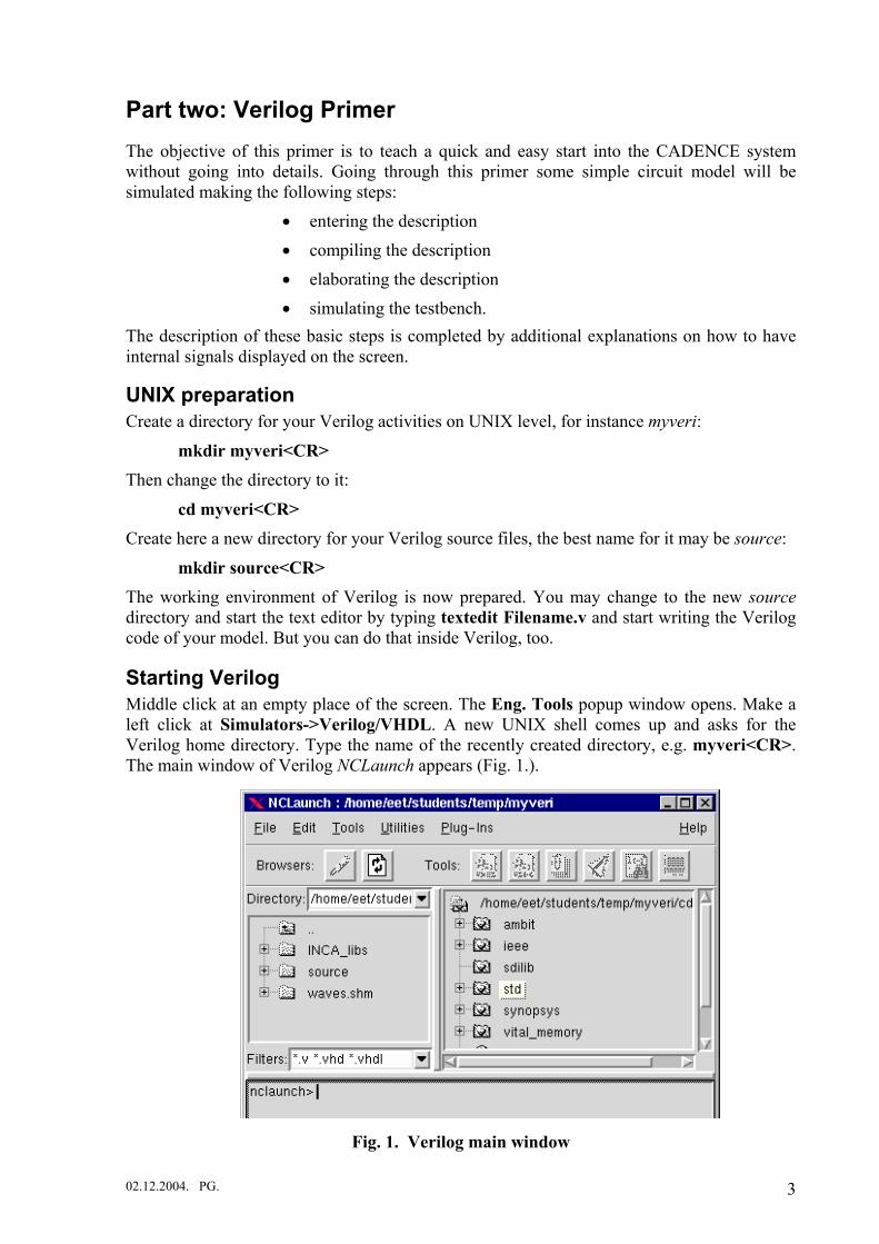
Starting Verilog Middle click at an empty place of the screen. The Eng. Tools popup window opens. Make a left click at Simulators->Verilog/VHDL. A new UNIX shell comes up and asks for the Verilog home directory. Type the name of the recently created directory, e.g. myveri<CR>. The main window of Verilog NCLaunch appears (Fig. 1.).
Fig. 1. Verilog main window
02.12.2004. PG. 3
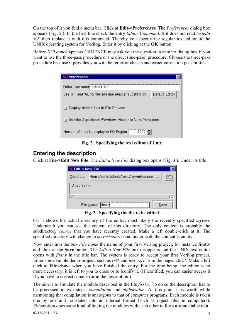
On the top of it you find a menu bar. Click at Edit->Preferences. The Preferences dialog box appears (Fig. 2.). In the first line check the entry Editor Command. If it does not read textedit %F then replace it with this command. Thereby you specify the regular text editor of the UNIX operating system for Verilog. Enter it by clicking at the OK button.
Before NCLaunch appears CADENCE may ask you the question in another dialog box if you want to use the three-pass procedure or the direct (one-pass) procedure. Choose the three-pass procedure because it provides you with better error checks and easier correction possibilities.
Fig. 2. Specifying the text editor of Unix
Entering the description Click at File->Edit New File. The Edit a New File dialog box opens (Fig. 3.). Under its title
Fig. 3. Specifying the file to be edited bar it shows the actual directory of the editor, most likely the recently specified myveri. Underneath you can see the content of this directory. The only content is probably the subdirectory source that you have recently created. Make a left double-click at it. The specified directory will change to myveri/source and underneath the content is empty.
Now enter into the box File name the name of your first Verilog project, for instance first.v and click at the Save button. The Edit a New File box disappears and the UNIX text editor opens with first.v in the title bar. The system is ready to accept your first Verilog project. Enter some simple demo-project, such as rsl1 and test_rsl1 from the pages 26/27. Make a left click at File->Save when you have finished the entry. For the time being, the editor is no more necessary, it is left to you to close or to iconify it. (If iconified, you can easier access it if you have to correct some error in the description.)
The aim is to simulate the module described in the file first.v. To do so the description has to be processed in two steps, compilation and elaboration. At this point it is worth while mentioning that compilation is analogous to that of computer programs. Each module is taken one by one and translated into an internal format (such as object files in computers). Elaboration does some kind of linking the modules with each other to form a simulatable unit. 02.12.2004. PG. 4
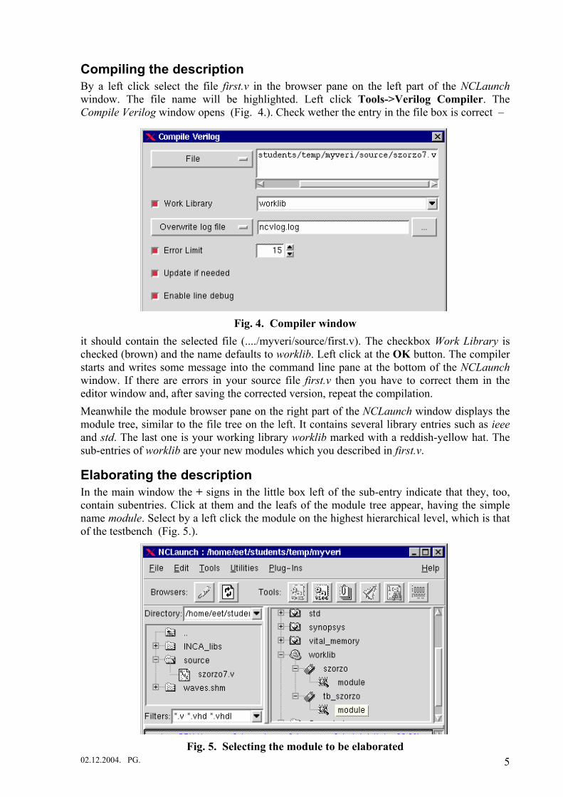
Compiling the description By a left click select the file first.v in the browser pane on the left part of the NCLaunch window. The file name will be highlighted. Left click Tools->Verilog Compiler. The Compile Verilog window opens (Fig. 4.). Check wether the entry in the file box is correct –
Fig. 4. Compiler window it should contain the selected file (..../myveri/source/first.v). The checkbox Work Library is checked (brown) and the name defaults to worklib. Left click at the OK button. The compiler starts and writes some message into the command line pane at the bottom of the NCLaunch window. If there are errors in your source file first.v then you have to correct them in the editor window and, after saving the corrected version, repeat the compilation. Meanwhile the module browser pane on the right part of the NCLaunch window displays the module tree, similar to the file tree on the left. It contains several library entries such as ieee and std. The last one is your working library worklib marked with a reddish-yellow hat. The sub-entries of worklib are your new modules which you described in first.v.
Elaborating the description In the main window the + signs in the little box left of the sub-entry indicate that they, too, contain subentries. Click at them and the leafs of the module tree appear, having the simple name module. Select by a left click the module on the highest hierarchical level, which is that of the testbench (Fig. 5.).
Fig. 5. Selecting the module to be elaborated 02.12.2004. PG. 5
Notice that only after you have selected a module, the icon of the elaborator (third from left among the tools in the icon bar, showing sheets of paper and a clip) will be enabled. Now it would be time to click at it, starting the elaborator. However, at the very first elaboration, the procedure is different.
Fig. 6. The window of the elaborator You have to make a left click at the menu item Tools->Elaborator which invokes the dialog box Elaborate (Fig. 6.). Check the followings: The Design Unit field should contain the name of your module. The checkbox Work Library should be checked (brown) and the field contain worklib. Access Visibility should also be checked and set to All. Correct the settings if necessary and click at the OK button. The elaborator starts and, after a while, some message appears in the command line pane. Check if there are errors reported.
After successful elaboration you can open the Snapshots folder in the module pane and you will find there your testbench module prepared for simulation (Fig. 7.).
Fig. 7. The elaborated module
Simulating the testbench Select the snapshot of the testbench module by a left click and then click at the icon of the simulator, fourth from left among the tools (or Tools->Simulator in the menu bar). The Cadence NC Verilog simulator window opens (Fig. 9, next page). The upper pane shows the source code of the actual scope, as a default the highest level, that is the testbench itself. Above the pane you can read the simulation time which is, before the start, zero. Later on, if you make several runs, you will have to left click Cadence NC Verilog:File->Reset Simulation before each new run if it differs from zero. Fig. 8. Highlighted names
Left click Select->Signals in the menu bar. In the source code all the signals appear highlighted (Fig. 8.). Now left click at Windows->Waveform. It takes some time (about 2 to 3 minutes!) till the window SimVision: Waveform opens (Fig. 10.). The waveform pane is still empty but the list of signals should be displayed in the left pane.
02.12.2004. PG. 6
Fig. 9. The simulation window
Fig. 10. The waveform window Now the simulation can be started by a left click on the big black triangle on the left side of the icon bar of the window Cadence NC Verilog. The simulation completes very quickly and the waveforms appear in the great pane of the waveform window (Fig. 11.). Above the upper
Fig. 11. The result of the simulation
02.12.2004. PG. 7
right corner you can find zooming buttons. At the upper left corner there are the small red flags of the cursors. They can be dragged by the left mouse button. In the narrow pane
between the signal list and the waveform the signal values can be read, at the simulation time indicated by the cursor TimeA.
Displaying internal signals So far only the signals of the highest level have been displayed. It is possible to go down in the hierarchy and display internal signals as well. Between the two large panes of the window Cadence NC Verilog there is the field for selecting the scope of the display. By clicking right of the Subscopes box at the small button with the black triangle a dropdown list appears showing the internal modules of the simulated system (Fig. 12.). Selecting one of them the actual source code text appears in the source code pane.
Fig. 12. Down in the hierarchy
If you need all the signals of the internal module then you can select them by means of the menu bar, with a left click at Select->Signals. Usually only some of them are needed. In such a case you can left click at them in the source code one by one. From the second one on, however, you have to keep the control key <CTRL> depressed. The selected signals will be highlighted. Having selected the signals you can transfer them into the waveform window by left clicking at the waveform button in the icon bar of SimVision: Waveform 1 (sixth one from right).
02.12.2004. PG. 8
Part three: Short Verilog Syntax This part describes the common Verilog language syntax supported by the Cadence tools that accept models written at the Register Transfer Level (RTL) of abstraction. Its objective is to provide a basis for working with the PKS circuit synthesis tool. The description is not complete but contains the most frequently needed and used constructs for the following two main types of tasks:
• Writing synthesizable Verilog code for circuit functions
• Writing testbenches for exercising the functions
Generally there is much similarity with the syntax of the C++ programming language, in those cases hints will be given.
Lexical Elements A Verilog source file is a stream of lexical tokens. A lexical token consists of one or more characters. The source file may be written in free format.
White Space: White space can contain the characters for blanks, tabs, newlines (CR, ENTER), and formfeeds. The only role of these characters is to separate other tokens.
Comments: Their syntax is identical with that of the C++ language, from // to the end of line or in block-form. from /* till */.
Numbers: Constant numbers can be specified in decimal, hexadecimal, octal, or binary format. Negative numbers are represented in 2's complement form. The usage of letters is not case sensitive. The base of decimal numbers may be omitted. Specifying the size in bits is optional, mainly if it has to be emphasized/forced. Examples:
43 = ’d43 = ’D43 = 6’b101011 = ’B101011 = ’o53 = ’O53 = ’h2b = 6’H2b
Strings: A string is a sequence of characters enclosed by double quotes and all contained on a single line. Example: „This is a string\n“.
Identifiers: An identifier is used to give an object, such as a register or a module or a wire, a name so that it can be referenced from other places. An identifier is any sequence of letters, digits, dollar signs ($), and the underscore '_' symbol. The first character must not be a digit or $; it can be a letter or an underscore. Identifiers are case-sensitive.
Keywords: They identify elements of the language consisting always of lower-case letters.
Data Types Value Set: The value set consists of four basic values:
The value Represents
0 A logic zero, or false condition
1 A logic one, or true condition
z A high-impedance state, not driven, floating.
x An unknown logic value, (may be 0, 1 or z)
Nets: The net data types represent physical connections between structural entities, their most frequently used type is the wire. A net does not store a value. Instead, it must be driven by a driver, such as a gate or a continuous assignment. They are usually declared but their “consequent usage“ can be accepted as implicite declaration. If the declaration does not specify the width then the default width is one bit (single net).
02.12.2004. PG. 9
Examples: wire apple, dog, abc, xx; // single wires wire [7:0] adr, dat; // 8-bit buses
Applying indices one particular bit or a contiguous part of the bus can be selected (bit or part select). (adr[4], dat[5:2])
Registers: A register is an abstraction of a data storage element (flipflop). A register is assigned a value as a consequence of some triggering event and then stores a value until the next one (procedural assignment). If it is assigned a value unconditionally in an always statement then it is automatically reduced to a wire. It is declared in the same form as a wire but using the keyword reg. Bit and part select apply as well. Examples: reg apple, dog, abc, xx; // single wires reg [7:0] adr, dat; // 8-bit buses
Integers: They are variables of register type. They are used in behavioural descriptions for counting events. They always have a predefined width of 32 bits. While registers store unsigned numbers integers are treated as two’s complements. Example: integer i, j, k;
Parameters: Parameters represent constants that can be used in many places in the description. Their usage is encouraged for the following reasons:
1. When making changes it is enough to change only the definition.
2. If there is a parameter defined in a module then each time the module is instantiated the parameter can be individually specified for that particular instance (parameter overriding, e.g. the width for each instantiated register).
3. Giving constants meaningful names makes reading and understanding the code easier.
Parameters can be defined using the keyword parameter: parameter width = 8; // width of a data bus parameter clockper = 50; // clock periode
Expressions An expression is a construct that combines operands with operators to produce a result. The result is a function of the values of the operands and the semantic meaning of the operators. Wherever a value is needed in a statement, an expression can be given. Even one single operand can be regarded as an expression.
The syntax as well as the semantics of the operators are almost identical with those of the C programming language, with only slight differences and so is their precedence, too.
Operands An operand can be one of the following:
• number • wire • register (integer) • bit- or part-select of wires or registers • a call to a function that returns any of the above
02.12.2004. PG. 10
Arithmetic Operators They are the unary operators: plus (+) and minus (-), the four basic arithmetic operators: + - * /, and the modulus operator: %.
Arithmetic expressions have to be applied carefully because Verilog treats registers as unsigned integers.
Relational Operators < <= Less than, less than or equal > >= Greater than, greater than or equal == != Equal, not equal
Comparing two operands yields 0 or 1. However, if, there are unknown bits in the operands then the result is x.
Logical Operators for single-bit operands && || AND, OR ! negation (inverted)
Bit-Wise Operators for bus-like operands ~ inversion, one’s complement & | AND, OR ^ ^~ ~^ XOR, XNOR (two possible versions)
When the operands are of unequal bit length, the shorter operand is zero-filled in the most significant bit positions.
Reduction Unary Operators & | ^ AND, OR, XOR ~& ~| ~^ ^~ NAND, NOR, XNOR
The unary reduction operators perform a bit-wise operation on a bus operand and produce a single bit result (e.g. with 8 bits & A results in 1 if A=‘hff, | A results in 0 if A=‘h00 and ^ A computes parity.)
Shift Operators << >> perform left and right shifts, the number of bit positions is given by the right operand. Both shift operators fill the vacated bit positions with zeroes.
Conditional operator: It has three operands (expressions) separated by two operators: <cond_expr> ? <true_expr> : <false_expr>
As <cond_expr> evaluates to true or false, one of <true_expr> and <false_expr> is evaluated and used as the result.
Concatenations: Expressions between the brace characters { and }, separated by commas, are joined together forming one vector. Examples:
{a,b,c}, {5{k}} (equal to {k,k,k,k,k}), {p,{2{q,r}}} (equal to {p,q,r,q,r})
02.12.2004. PG. 11
Assignments In an assignment the expression on the right-hand-side of the equal sign (=) is evaluated and its result is assigned to the variable on the left-hand side. Latter can be register or wire, single or bus, bit or part select. The selection must be made by constant numbers. The assignment can be continuous or procedural.
Continuous Assignments Continuous assignments drive values onto nets (wires). The word continuous is used to describe this kind of assignment because the assignment is always active. Whenever simulation causes the value of the right-hand side to change, the assignment is re-evaluated and the output is propagated. Continuous assignments provide a way to model combinational logic without specifying an interconnection of gates. Its form is:
assign <net_type_variable> = <expression>
There is no restriction for <expression>, it may be a call to a function, too.
Procedural Assignments Procedural assignments can only assign values to registers (integers). Procedural assignments occur only within procedures, such as always and initial statements. The assignment is triggered. It is only executed when the flow of execution reaches an assignment within a procedure. Reaching the assignment can be controlled by conditional statements (if, case).
The left-hand side can be single register or vector (bus), bit or part select. The selection must be made by constant numbers.
Behavioral Modeling All procedures in Verilog are specified within one of the following four statements:
always statement initial statement task function
Tasks and functions are procedures that are enabled from one or more places in other procedures. They are not covered in this description.
The initial and always statements are enabled at the beginning of simulation. The initial statement executes only once while the always statement executes repeatedly. There is no limit to the number of initial and always blocks that can be defined in a module.
The syntax of the always construct: always <statement> The syntax of the initial construct: initial <statement>
Blocking and Non-Blocking Procedural Assignments A blocking procedural assignment statement is executed before the execution of the statements that follow it in a sequential block. Its form is:
<register> = [ timing_control ] expression
The non-blocking procedural assignment allows assignment scheduling without blocking the procedural flow. Its form is:
<register> <= [ timing_control ] expression
For the optional timing control see details at the Intra-assignment timing control (page 17)
02.12.2004. PG. 12
Conditional Statements A statement is conditionally executed by means of the if-statement:
if (expression) <statement>
The if-else statement chooses from two statements to execute one:
if (expression) <statement> else <statement>
The if-else-if statement executes one of several statements:
if (expression) <statement> { else if (expression) <statement> } can be repeated without limit! [ else <statement> ]
The if-construct selects the statement to be executed on the basis of different expressions which evaluate to true/false (or 1/0). On the contrary, the case statement takes one expression that can evaluate to several different values and the basis of the selection is: to which of several other expressions (they are almost always constant expressions) is it equal. If none of them happens to be equal to the selecting expression then no statement is executed. For such a case the default condition and statement may be specified:
case (expression) expression_1: statement_1; expression_2: statement_2; expression_3: statement_3; ………………. expression_n: statement_n; default: default_statement; endcase
If you want to use don’t care bits (?), too, in the conditions (expression_I) then you have to use the statements casez and casex. Casez can process the value z in the positions marked by ? while casex can accept both z and x.
Conditional statements can be used only in sequential procedural blocks.
Looping Statements
There are three types of looping statements that provide a means of controlling the execution of a statement, either zero, one, or more times. In the case of repeat the number of repetitions is prescribed. In the case of while the condition of execution is given, if it evaluates to zero already at the beginning then the statement will not be executed at all. The for statement is just the same as in the programming languages:
repeat (number_of_executions) <statement> while (condition_of_executions) <statement> for (reg_assignment ; condition_of_executions ; reg_assignment) <statement>
The looping statements can be used either for signal processing in behavioural descriptions just like in programming languages or for building periodic circuit structures in complex systems (e.g. instantiating a series of full adders using one looping statement for forming a multi-bit adder module).
02.12.2004. PG. 13
Procedural Event Control The execution of a procedural statement can be synchronized with a value change on a net or register. Its syntax is:
@ (expression)
Usually, the expression is the name of a register or wire alone or several such elements combined by the keyword or. The synchronizing effect can be coupled to the direction of the change by the keywords posedge or negedge.
Delayed Statement Execution
The execution of a procedural assignment can be delayed after the execution of the previous statement in the description. In case of a blocking statement the simulator waits for the specified delay time to expire. In that particular process nothing happens in between. Then the statement is executed and the simulator processes the following statement. The syntax of the delay is:
# <constant> <statement> # (<expression>) <statement>
The delay is not synthesizable, it can be applied solely in behavioural descriptions. It is mainly used in testbenches for the description of time-dependent input signals.
Intra-Assignment Timing Control (delayed assignment) In contrast to the delayed statement execution here only the assignment of the new value is delayed while the control is going on to the following statements. The syntax is slightly different:
<register> = # <constant> <expression> <register> = # (<expression>) <expression>
This syntax implies a certain hidden internal storage. # <constant> or # (<expression>) specify the delay. When it comes to the execution of the statement then the expression to be assigned on the right-hand side is sampled and evaluated without delay. However, the result of the evaluation will not be assigned to the register on the left-hand side before the specified delay elapses. Meanwhile the expression may change but the sampled value will be stored and assigned.
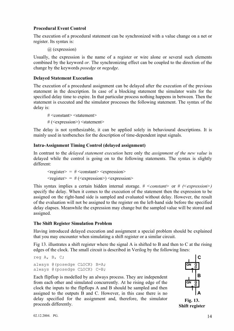
The Shift Register Simulation Problem Having introduced delayed execution and assignment a special problem should be explained that you may encounter when simulating a shift register or a similar circuit.
Fig 13. illustrates a shift register where the signal A is shifted to B and then to C at the rising edges of the clock. The small circuit is described in Verilog by the following lines:
Fig. 13. Shift register
A
CQN Q
D
BQN Q
D
reg A, B, C;
always @(posedge CLOCK) B=A; always @(posedge CLOCK) C=B;
Each flipflop is modelled by an always process. They are independent from each other and simulated concurrently. At he rising edge of the clock the inputs to the flipflops A and B should be sampled and then assigned to the outputs B and C. However, in this case there is no delay specified for the assignment and, therefore, the simulator proceeds differently.
02.12.2004. PG. 14
‘No delay’ is interpreted by the simulator that the assignment may take place instantly. Processing the first always block the value of A is assigned to B without delay. Processing the second always block the value of B is assigned to C – but this is no more the original value of B which it had just before and at the rising edge of the clock.. The concurrency of the simulation is lost. The result is not correct (it might be in this case if the order of processing were different).
What is wrong? On one hand the simulator may be blamed that it does not consequently execute concurrent simulation. On the other hand, however, from a theoretical point of view, with zero delay concurrency cannot be clearly defined, so blaming is only partly justified.
So what to do? The workaround is simple. With a slightly delayed assignment the simulation is perfect and, important, it is ignored by the synthesis tool, it does not disturb the synthesis: always @(posedge CLOCK) B=#1 A; always @(posedge CLOCK) C=#1 B;
The Structure of Verilog Models The basic unit of Verilog descriptions is the module. It is delimited with the keywords module and endmodule. It exchanges information with the rest of the world via input and output (or bidirectional inout) ports. The ports have to be declared in the port list, and the elements of the list have to be specifyed if they are input, output or inout. If a port is not only a single signal but a bus or vector then its width has to be declared by specifying two index limits as well. The first index is always the most significant bit (msb) while the second one is the least significant bit (lsb). The indices are non-negative integer numbers. Accordingly, the frame of the module surrounding the body should look like this: module name(p1, p2, p3, ... pn); input p1, p2; input [msb1 : lsb1] p3; output p4, p5; output [msb2 : lsb2] p6; ... ... Body of the module ... ... endmodule
The body of the module has to describe the elements which process the input signals to form the outputs. Such elements are:
• Parameter declaration • Register declaration • Wire declaration • Continuous assignment (assign) • initial structure • always structure • Other modules instantiated in the body of the module
The output ports have to be driven inside of the module by signal sources. There are two main signal sources having driving capabilities:
• Registers (abstraction of a flipflop) • Continuous assignments (abstraction of a combinational logic function)
02.12.2004. PG. 15
• Additionally, in case of hierarchy, other modules instantiated in the body of the module and having an output which is driven by a driving element inside.
If the output is driven by a register (procedural assignment) then the identifier of the output has to be declared as register. If the output is driven by a continuous assignment or by the output of a module instance then its identifier has to be declared as wire. The input ports form signal sources have to be declared as wires.
While the input signals are processed, other (auxiliary) internal signals may be generated for which, too, registers and wires have to be declared.
The activities are described by assignments which are placed into assign, initial or always constructs.
If some operational function has already been described in a module of its own then one or several instances of it may be built into other modules. This will be explained in the next section.
Hierarchical Structures The basic unit of Verilog descriptions is the module. The Verilog HDL supports a hierarchical hardware description structure by allowing modules to be embedded within other modules. Higher-level modules create instances of lower-level modules and communicate with them through ports. Each module definition stands alone, is independent from the others. Statements within the module definitions create instances of other modules, thus describing the hierarchy.
Module Instantiation The instance is defined by referencing its modul-name, a unic instance-name (identifier) and specifying the port connection list: <modul-name> <instance-name> (<port connection list>); Inside a module each instance-name has to be unic, even if identifying different types of modules. If the designer omits the instance names then the compiler automatically assigns unic identifiers to each module, however, these will not be meaningful, easy-to-remember names.
Connecting Module Ports
The ports are connected to the registers and wires of the calling module. The mapping can be organized by name or by an ordered list (by position). The method of the ordered list is just the same as it is done when subroutines are called in a computer program. The connected elements have to be listed in the same order as they are in the definition of the module. Care should be taken to map wires (and not registers) to be driven to the output ports of the instance and to map driving elements to the input ports (either registers or wires driven by other sources such as assign statements or outputs of other module instances). The elements of the list are separated by commas. If an output port is not used and, therefore, not connected then a space character has to be placed into the list, separated by a comma. The next lines show the declaration of an RS-latch and how this module is called from higher hierarchical level for representing a flag while the inverted output is left unconnected: module rsl1(q,qn,preset,clear);
rsl1 latch(flag, ,set,reset);
Connecting ports by name is done by explicitly linking the two names for each side of the connection. The link is introduced by a dot character, followed by the name used in the module definition, followed by the terminal used in the calling module in parentheses. The
02.12.2004. PG. 16
port order is irrelevant, not connected outputs need not be listed. However, all input ports must be driven. The two methods of connection may not be mixed. The previous instantiation of the latch with connections by name:
rsl1 latch(.clear(reset), .preset(set),.q(flag));
Overriding Module Parameter Values When one module instantiates another module, it can alter the values of any parameters declared within the instantiated module. (E.g. the width of a register or the length of a counter can be adapted to the size of the calling module.) In this case the module instantiation is added a parameter specification:
<modul-name> <parameter-specification> <instance-name> (<port connection list>);
The parameter specification has the following form:
#(list-of-expressions)
The list of expressions has to cover all the parameters defined in the instantiated module, in the same order as they are defined, even if some of them should not be altered.
The testbench, its role and structure We describe a specified function by an HDL in order to verify it by simulation and to create a realizable circuit design for it, possibly by synthesis. The would-be circuit is simulated in its future environment which provides the input signals for it and which receives and, if necessary, processes its output signals. Such an environment is simulated for a module to be verified by the testbench.
The testbench itself is a module, too. However, it is a special one in that it does not have ports, for it is „the rest of the world“ for the module to be tested. The module to be tested is embedded into the testbench as an instance. The testbench contains descriptions of time-dependent signals to drive the inputs of the module to be tested. Therefore, the testbench is not synthesizable. If it is described in the same file as the module to be verified then the synthesis program has to be instructed by directives not to try to synthesize it because it would only result in error messages.
In other respects the testbench is just a normal module. In addition to the module to be tested it may contain embedded instances of other modules, too. The minimal testbench contains the module to be tested and an initial process where the input signals are described using simple delayed assignments (#<delay> <assignment>;) and – very important – the end of the simulation is specified with the $finish keyword.
It is quite a trivial fact that complex modules need complicated input sequences which are not easy to describe and produce complicated output waveforms which are often tiresome to evaluate. It is up to the designer how she/he organizes these tasks. It is possible to describe each input signal in a separate initial or always process or to group several of them, having similar waveforms, into one process. Here is a simple example presented for generating the clock signal: parameter cp=100; // 100 nsec clock period reg CLK; initial CLK=0; // it must start wit a well-defined value always #(cp/2) CLK=!CLK; // invert it after each half period
02.12.2004. PG. 17
Generating or checking complex waveforms is not only difficult but also error prone. It is worth while investing some work into building a testbench which can do these jobs partly or fully automatically. Just a simple example: in case of modules having serial data input/output
functions it can be very helpful to equip the testbench with parallel-serial conversion for producing input series easily, and serial-parallel conversion for comfortable checking serial output signals. Maybe you can fetch such modules from other projects and embed them into the testbench. If the module to be tested outputs a signal to some external unit and later expects some answer from it at an input port then it pays off to define a process which, after some delay, automatically generates the answer. All in all, a well-organized testbench can simplify and accelerate the functional verification at a great extent.
Verilog and Synthesis In this section the elements of the Verilog language are surveyed with respect to their role in circuit synthesis. Although this survey is based upon the rules of the Cadence PKS synthesis program, the situation can be regarded as typical. On one hand PKS, just like other synthessis programs, tries to exploit all theoretically usable constructs, and, on the other hand, PKS is a highly sophisticated modern synthesis tool.
Support of Verilog constructs From synthesis point of view Verilog constructs can form four categories:
1. Fully supported constructs. They can be used unconditionally in describing a model. These include the basic module declaration, instantiation, use of reg and wire data types, continuous assignments, always procedural blocks, and many of the procedural statements. They will be described in detail later.
2. Partially supported constructs. They can be used under specific conditions. When those conditions are not met, an error message is generated. Examples of them:
the operands ‘/’ and ‘%’ (division and modulo) are supported only if the right-hand operand evaluates to a constant power of two (then they reduce to shift operations!). posedge, negedge are only supported in the sensitivity list of an always construct. always is only supported with triggered events with @(…). Blocking (=) and non blocking (<=) assignments cannot be mixed in a conditional statement, such as if or case, or in bitwise assignments.
3. Ignored constructs. They are ignored when a Verilog HDL model is read into the synthesizer. Examples of them:
Delay specification on continuous assignments. Signal strengths in continuous assignments. Intra-assignment timing controls in procedural statements. wait
Using such constructs may have the consequence that the synthesized circuit simulates differently from the original high level model description.
4. Unsupported constructs. When these costructs are encountered in a Verilog HDL model then an error message is generated. Examples of them:
event data types, trireg data types, initial procedural block, fork, join, defparam.
02.12.2004. PG. 18
Modeling style (constructs and synthesis) Using the supported constructs it is always possible to write synthesizable Verilog code, resulting in circuits which realize the function that was modeled, performing the same simulation results. However, the effectiveness of the synthesis is not independent from the structure of the HDL code. In the followings those constructs will be shown which can be favourably used for writing synthesizable Verilog code, together with explanations about the resulting circuit structures.
Modeling combinational logic
Each continuous assignment – assign statement – infers a combinational network, since changes of the inputs (right-hand side) instantanously (with a gate delay) propagate to the output (left-hand side). For example, the next statement will generate a three-input OR-gate:
reg a, b, c; wire y; assign y = a || b || c;
Similarly, the synthesis tool generates a four-input AND-gate from the next lines containing a reduction unary operator:
reg [7:0] qq; wire y; assign y = & qq[6:3];
In procedural assignments the left-hand side variables are registers. Yet if the sensitivity list of the always procedure contains each input variable of the assignment then the synthesis of the next constructs results in combinational logic.
1. The variable is unconditionally assigned a value before it is used at all, and then each time when the right-hand side changes:
wire a, b, c; reg y; always @(a or b or c) begin y = a + b + c; end
This construct results in a three-input combinational adder circuit.
2. The variable is conditionally assigned a value in each case when on the right-hand side something changes:
wire a, b, s; reg z; always @(a or b or s) begin if (s) z=a; else z=b; end
This will be synthesized as a two-input multiplexer where the variable s selects a or b from the inputs.
02.12.2004. PG. 19
Synthesis of registers There are two basic forms, the synthesis of the level-sensitive latch and that of an edge-triggered flipflop:
reg q; wire d, en; always @(en or d) if (en) q=d;
Here q is assigned the new value of d as long as en=1. If en is reset to zero then q does not change any more. This function is realized by a latch. The next example is a typical model of an edge-triggered flipflop, where assignment only occurs at the positive edge of the clock:
reg q; wire d, clk; always @(posedge clk) q=d;
Asynchronous and synchronous set/reset The synchronous set/reset (concerning only flipflops) is somewhat simpler in that the procedure is activated only by the edge of the clock. The priority of set or reset depends upon which is coming first in the if-then-else statement (for sake of simplicity declarations will be omitted in the followings):
always @(posedge clk) begin if (set) q=1’b1; else if (reset) q=1’b0; else q=d; end
In the asynchronous version the signals set and/or reset have to be included in the sensitivity list. In case of flipflops:
always @(posedge clk or posedge reset) if (reset) q=1’b10; else q=d;
If the reset signal is active low then negedge reset and !reset have to be used: always @(posedge clk or negedge reset) if (!reset) q=1’b10; else q=d;
The case of latches is quite similar with the only difference that the sensitivity list will not contain edges. A simple example of a latch with reset can illustrate it:
always @(en or res or d) if (res) q=1’b10; else if (en) q=d;
With flipflops it may happen that both synchronous and asynchronous versions are necessary. Let set be the asynchronous signal and preset the synchronous one:
always @(posedge clk or posedge set) begin if (set) q=1’b1; else if (preset) q=1’b1; else q=d;
02.12.2004. PG. 20 end
This construct might be simplified by uniting the two setting conditions: if (set || preset) q=1’b1;
This is a correct Verilog statement and it would simulate correctly. However, in this form the tool Ambit BuildGates cannot recognize to what circuit/logic elements should it be mapped and generates an error message. It is worth while mentioning that the synthesis tool is not sensitive for variable names. It looks rather for given syntactic constructs defined by the relative position of keywords than the variables clock or reset, etc..
In addition, it is not recommended to define more than one register in one always construct but it is definitely faulty to assign values to a given register in more than one always construct.
Just one more example to illustrate how the synthesizer “thinks”. Supposing there is in the technology library a D type flipflop with double-rail outputs Q and QBAR. How can the designer use this feature? He might declare two registers Q and QBAR and write the following code:
reg Q, QBAR; wire D; always @(posedge clk) begin Q=D; QBAR=!D; end
This code looks logic but PKS will infer two generic flipflops and assign D and !D to them, respectively. Such a circuit will have the correct function, however, it will surely not be optimal. To get the desired structure of using both outputs of one flipflop the code should be:
reg Q; wire QBAR; always @(posedge clk) begin Q=D; end assign QBAR=!Q;
Encountering this code, in the first run PKS will take a flipflop and an inverter but in the optimizing phase it will eliminate the inverter and use the double-rail flipflop.
Case statements
The synthesis of case statements can result in several different circuit structures depending upon how the branching statements are organized. The most simple case is when constants are assigned to the same variable in all the branches. This will be processed by the generator AWPLA. If the branching is “full” (e.g. 8 assignments controlled by a 3-bit variable) then a ROM is generated, if not “full” then PLA – but only if there is a default statement for all the input values which are not explicitely enumerated and specified. If there is no default branch in a not-full case statement then a latch will be inferred which will hold the result of the previous assignment while the input has changed and there is no branch specified for the new value. However, if the designer can guarantee that the not specified values will never turn up then she/he can enforce the generation of combinational logic by a full case directive which tells AWPLA to handle the statement as if it were full.
The next example of a casex statement illustrates a simple case for the synthesizer tool. The four case items of the 4-bit input variable sel each form a branch according to which bit
02.12.2004. PG. 21
contains a High. The other bits are don’t care and are masked by x’s. In order to avoid the generation of a latch a default item is also included. The result of the synthesis is a priority encoder.
reg [1:0] y; wire [3:0] sel; always @( sel) casex (sel) 4’bxxx1: out = 2’b00 4’bxx1x: out = 2’b01 4’bx1xx: out = 2’b10 4’b1xxx: out = 2’b11 default: out = 2’bxx endcase
Another important version of the case statement is when different signals are assigned to the output depending upon a selection variable. In such a case the AWMUX generator builds a multiplexer. If the case statement is full or it contains a default or a full case directive is given then the result is pure combinational. If neither of these conditions is fulfilled then a latch will be inferred.
02.12.2004. PG. 22
Part four: Examples The following examples illustrate the construction of the description of circuits and functions by means of the Verilog HDL. They are furnished with ample comments for the sake of readability and understandability. For the same purpose indentation has been thoroughly applied. They should help you build your own modules. After a simple RS-latch (for exercising work with the simulator) two full descriptions are given with test-bench. The multiplier shows two versions of the same problem. The first version is the simplest possible behavioural description of an 8 by 8 bit multiplier. It just multiplies the two numbers producing the 16-bit result. The second version was modelled with practical realizability (and possible synthesis) in mind, and, in addition, the corresponding circuit is presented in Figs. 15. and 16. The model is not directly synthesizable because it does not have an explicite reset input. Instead, the starting values are specified in initial statements. It may be a good exercise for the reader to replace them by providing an “ordinary” resetting circuitry. This restriction holds for the next example, too.
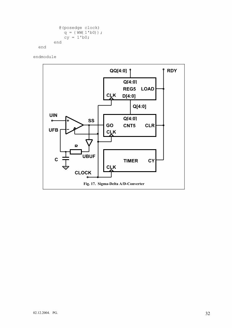
The second example is an analog/digital converter (ADC). It is a mixed-signal system in that its input is an analog signal which is connected to an analog comparator. The reference (negative) input of the comparator gets feed-back from the output of the comparator integrated by an RC integrator circuit. These parts of the system are described only on the behavioural level. The rest of the system is fully digital and is modelled again with synthesis in mind. Here, too, the corresponding circuit is also given (Fig. 17.).
Note that while Verilog is basically digital, the built in mathematical apparatus for functional descriptions offers excellent possibilities for modeling “quasi-analog” signals and circuits. The usage of real numbers and variables is somewhat restricted but it is always possible to define long multibit registers and buses for holding quasi-analog quantities. Using 32-bit registers voltages can be processed and stored in microvolts. Such a resolution is only seldom not enough to simulate quasi-analog signals. Of course these parts are not sythesizable but with this workaround the complete system can be simulated
The Very First Verilog Model: an RS-Latch In the followings a very simple Verilog model is presented, that of an RS-latch, consisting of two cross-coupled NAND gates. You may take it as your first Verilog description for building and simulating it. (Fig. 14.) module rsl1(q, nq, preset, clear);
PRESETCLEAR
NQ Q output q, nq; input preset, clear; reg q, nq; always @(preset or nq) #1 q = !(nq && preset); always @(clear or q) Fig. 14. RS-latch #1 nq= !(q && clear); endmodule
Here follows a testbench of the RS-latch which takes the latch rsl1 as an instance and provides input signals to it: module rsl1_test; wire q, nq; // declare two wires to receive outputs reg preset, clear; // declare two input variables
02.12.2004. PG. 23 parameter d = 10; // used as the waveform time step
// create an instance of the RS-latch rsl1 latch(q, nq, preset, clear); // stimulus description - assigns values to inputs initial // runs only once begin preset = 0; clear = 1; #d preset = 1; #d clear = 0; #d clear = 1; end endmodule //....................................................
// The most simple multiplier (behavioral description) //=========================================================== // using a continuous assignment and zero delay `timescale 100ns/1ns module szorzo(szorzat, szorzando, szorzo); output [15:0] szorzat; input [7:0] szorzando; input [7:0] szorzo; wire [15:0] szorzat; assign szorzat = szorzando * szorzo; endmodule // end of the multiplier module //.................................................... module tb_szorzo; // Testbench of the multiplier wire [15:0] product; reg [7:0] multiplicand; reg [7:0] multiplier; szorzo mult(product, multiplicand, multiplier); initial begin multiplicand = 8'h3; multiplier = 8'h0; #10 multiplier = 8'h4; #10 multiplier = 8'h6; #10 multiplier = 8'h8; #10 $finish; end endmodule
// Multiplier circuit (detailed RTL description)
02.12.2004. PG. 24//===================================================
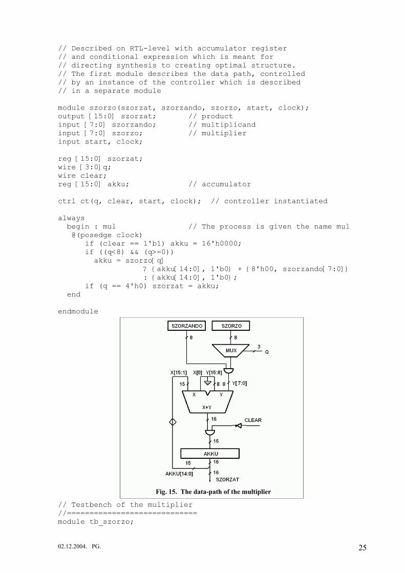
// Described on RTL-level with accumulator register // and conditional expression which is meant for // directing synthesis to creating optimal structure. // The first module describes the data path, controlled // by an instance of the controller which is described // in a separate module module szorzo(szorzat, szorzando, szorzo, start, clock); output [15:0] szorzat; // product input [7:0] szorzando; // multiplicand input [7:0] szorzo; // multiplier input start, clock; reg [15:0] szorzat; wire [3:0]q; wire clear; reg [15:0] akku; // accumulator ctrl ct(q, clear, start, clock); // controller instantiated always begin : mul // The process is given the name mul @(posedge clock) if (clear == 1'b1) akku = 16'h0000; if ((q<8) && (q>=0)) akku = szorzo[q] ? {akku[14:0], 1'b0} + {8'h00, szorzando[7:0]} : {akku[14:0], 1'b0}; if (q == 4'h0) szorzat = akku; end endmodule
Fig. 15. The data-path of the multiplier
// Testbench of the multiplier //============================= module tb_szorzo;
02.12.2004. PG. 25
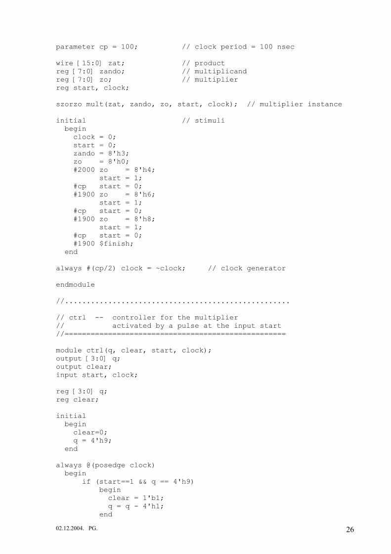
parameter cp = 100; // clock period = 100 nsec wire [15:0] zat; // product reg [7:0] zando; // multiplicand reg [7:0] zo; // multiplier reg start, clock; szorzo mult(zat, zando, zo, start, clock); // multiplier instance initial // stimuli begin clock = 0; start = 0; zando = 8'h3; zo = 8'h0; #2000 zo = 8'h4; start = 1; #cp start = 0; #1900 zo = 8'h6; start = 1; #cp start = 0; #1900 zo = 8'h8; start = 1; #cp start = 0; #1900 $finish; end always #(cp/2) clock = ~clock; // clock generator endmodule //.................................................... // ctrl -- controller for the multiplier // activated by a pulse at the input start //=================================================== module ctrl(q, clear, start, clock); output [3:0] q; output clear; input start, clock; reg [3:0] q; reg clear; initial begin clear=0; q = 4'h9; end always @(posedge clock) begin if (start==1 && q == 4'h9) begin clear = 1'b1; q = q - 4'h1; end
02.12.2004. PG. 26
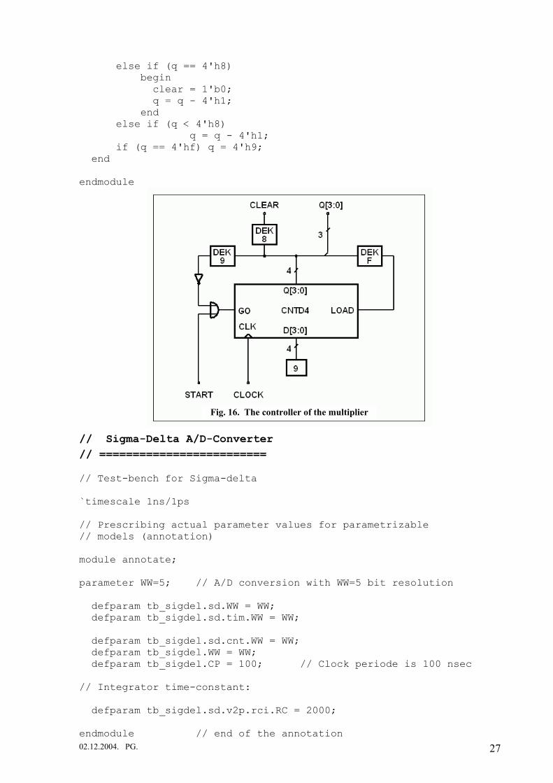
else if (q == 4'h8) begin clear = 1'b0; q = q - 4'h1; end else if (q < 4'h8) q = q - 4'h1; if (q == 4'hf) q = 4'h9; end endmodule
Fig. 16. The controller of the multiplier
// Sigma-Delta A/D-Converter // ========================= // Test-bench for Sigma-delta `timescale 1ns/1ps // Prescribing actual parameter values for parametrizable // models (annotation) module annotate; parameter WW=5; // A/D conversion with WW=5 bit resolution defparam tb_sigdel.sd.WW = WW; defparam tb_sigdel.sd.tim.WW = WW; defparam tb_sigdel.sd.cnt.WW = WW; defparam tb_sigdel.WW = WW; defparam tb_sigdel.CP = 100; // Clock periode is 100 nsec // Integrator time-constant: defparam tb_sigdel.sd.v2p.rci.RC = 2000;
02.12.2004. PG. 27endmodule // end of the annotation
module tb_sigdel; // begin of the test-bench parameter WW=8, CP=1000; // Parameters superseded by annotation reg [15:0] uin; // Quasi-analog input voltage reg clock; wire [(WW-1):0] q; // Converted result wire rdy; // Conversion done sigmadelta sd(q, rdy, uin, clock); // instance of the converter always #(CP/2) clock = ~clock; // clock generator initial // specifying (quasi-)analog input voltages begin clock = 0; uin = 0; #250 uin = 16'h7000; #5000 uin = 16'hffff; #15000 uin = 16'h9000; #5000 uin = 16'h0; #15000 $finish; end endmodule //............................................................ // The Top-Level Module of the Sigma/Delta A/D-Converter //======================================================= // It only contains the submodules and an output register module sigmadelta(qq, rdy, uin, clock); output qq; output rdy; input [15:0] uin; input clock; parameter WW=8; wire [(WW-1):0] q; wire rdy, ss; // the output register qq captures and holds the converted // value till the next conversion is done reg [(WW-1):0] qq; initial qq=0; always @(posedge clock) if (rdy) qq = q; volt2puls v2p(ss, uin, clock); // voltage/pulse converter counter cnt(q, ss, rdy, clock); // ones´s counter timer tim( , rdy, clock); // time basis, output q is not used
02.12.2004. PG. 28
endmodule //............................................................ // Voltage-to-pulse converter //============================ // converts analog voltage to a stream of pulses module volt2puls(q, uin, clock); output q; input uin; input clock; // Quasi-analog voltages: wire [15:0] uin; // input wire [15:0] ufb; // feed-back wire [15:0] ubuf; // buffer of comparator output wire q; // original comparator output, digital // It just contains 3 sub-modules komp cmp(q,uin,ufb,clock); // Comparator output_buffer bf(ubuf, q); // Buffer generating analog output rcint rci(ufb, ubuf, clock); // Feed-back RC integrator endmodule //............................................................ // Clocked analog comparator with quasi-analog integer input //=========================================================== module komp(q,ux,uref, clock); output q; input [15:0] ux; input [15:0] uref; input clock; reg q; initial q=0; always @(posedge clock); q = uref<ux; endmodule //............................................................ // Output buffer, producing quasi-analog output voltage. //======================================================= // Input: logic 0 and 1; Output: 16-bit quasi-analog integer // values 16'h0000 and 16'hffff
02.12.2004. PG. 29
module output_buffer(qa,din); input din; // digital input output qa; // quasi-analog output reg [15:0] qa; always @din qa = din ? 16'hffff : 16'h0000 ; endmodule //............................................................ // Integrator //============ // Integrating RC feedback circuit for sigma-delta A/D // conversion, with quasi-analogous 16-bit integer variables. // The voltage range 0...5V is mapped from 'h0000 to 'hffff // Realizes the equation duout = (uin - uout)*dt/RC // Signs are separated because regs store unsigned numbers module rcint(uout, uin, clock); output uout; input [15:0] uin; input clock; parameter RC = 3000; // integrator time constant // for correct operation RC >= 10*clock-period reg [15:0] uout; reg [15:0] delu1; reg [15:0] delu2; time delt, tprev; always @(posedge clock) begin delt = $time - tprev; // dt tprev = $time; if (uin<uout) // Increasing output begin delu1 = uout-uin; delu2 = delu1*delt/RC; uout = uout - delu2; end else // Decreasing output begin delu1 = uin-uout; delu2 = delu1*delt/RC; uout = uout + delu2; end end initial begin uout = 0; tprev = 0; end
02.12.2004. PG. 30
endmodule //............................................................ // counter //========= // WW bits wide counter with synchronous clear // for counting the ones in the input stream module counter(q,go,clear,clock); output q; input go, clear,clock; parameter WW=8; reg [(WW-1):0] q; initial q=0; always begin @(posedge clock) if (go) q = q + 1'b1; if (clear) q = {WW{1'b0}}; end endmodule //............................................................ // Timer //======= // provides the time basis for the A/D conversion // WW bits wide counter, carry=1 when its value is all-ones
module timer(q,cy,clock); output q, cy; input clock; parameter WW=8; reg [(WW-1):0] q; reg cy; initial begin q=0; cy=0; end always begin @(posedge clock) q = q + 1'b1; if (q == {WW{1'b1}}) begin
02.12.2004. PG. 31 cy = 1'b1;
@(posedge clock) q = {WW{1'b0}}; cy = 1'b0; end end endmodule
RDY
Fig. 17. Sigma-Delta A/D-Converter
UBUF
SS
Q[4:0]
CLOCK
UFB
UIN
C
R
QQ[4:0]
CLKLOAD
D[4:0]
Q[4:0]REG5
CLKCYTIMER
CLKCLRGO
Q[4:0]CNT5
02.12.2004. PG. 32