verilog 1 - fundamentalscsg.csail.mit.edu/.../handouts/lectures/l02-verilog-fundamentals.pdf · •...
TRANSCRIPT

Verilog 1 - Fundamentals
6.375 Complex Digital SystemsChristopher BattenFebruary 9, 2006
FA FA FA FA module adder( input [3:0] A, B,output cout,output [3:0] S );
wire c0, c1, c2;FA fa0( A[0], B[0], 1’b0, c0, S[0] );FA fa1( A[1], B[1], c0, c1, S[1] );FA fa2( A[2], B[2], c1, c2, S[2] );FA fa3( A[3], B[3], c2, cout, S[3] );
endmodule
6.375 Spring 2006 • L02 Verilog 1 - Fundamentals • 2
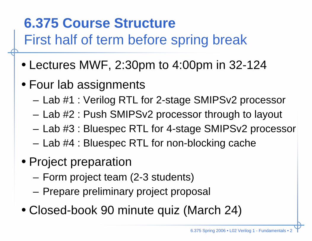
6.375 Course StructureFirst half of term before spring break
• Lectures MWF, 2:30pm to 4:00pm in 32-124• Four lab assignments
– Lab #1 : Verilog RTL for 2-stage SMIPSv2 processor– Lab #2 : Push SMIPSv2 processor through to layout– Lab #3 : Bluespec RTL for 4-stage SMIPSv2 processor– Lab #4 : Bluespec RTL for non-blocking cache
• Project preparation– Form project team (2-3 students)– Prepare preliminary project proposal
• Closed-book 90 minute quiz (March 24)

6.375 Spring 2006 • L02 Verilog 1 - Fundamentals • 3
6.375 Course StructureSecond half of term after spring break
• Weekly project meetings with instructors• Weekly milestones with 1-2 page report• Final project presentations last week of classes• Final project report
– Approximately 15-20 pages– Due May 17 (no extensions!)

6.375 Spring 2006 • L02 Verilog 1 - Fundamentals • 4
6.375 Course StructureSemester long design project
• Two standard projects with fixed interfaces, infrastructure, and testbenches– SMIPS microprocessor
• High performance (e.g. multicore, ooo superscalar)• Low power (e.g. fetch throttling, instruction fusion)• Minimal area (e.g. multiplexed byte-wide datapath)
– SMIPS memory system• Cache-coherent multicore• DRAM memory access scheduler• Hardware prefetching

6.375 Spring 2006 • L02 Verilog 1 - Fundamentals • 5
6.375 Course StructureSemester long design project
• Custom or non-standard projects– Submit 2 page proposal by March 17 for approval– C/C++/Java reference implementation by March 22– Ex: MP3 player, graphics pipeline, network processor
802.11a Encoder, 2005

6.375 Spring 2006 • L02 Verilog 1 - Fundamentals • 6
6.375 Course StructureGrade breakdown
Four labs 30%Quiz 20%Project milestones 25%Final project report 25%
6.375 Spring 2006 • L02 Verilog 1 - Fundamentals • 7
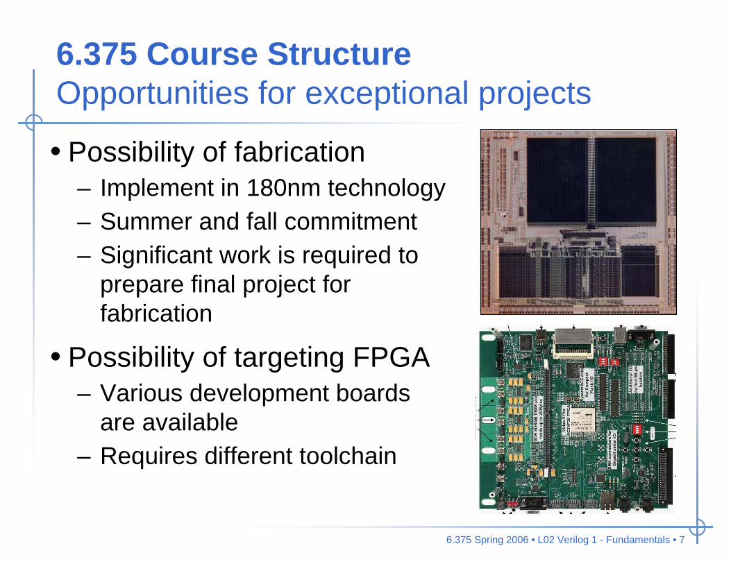
6.375 Course StructureOpportunities for exceptional projects
• Possibility of fabrication– Implement in 180nm technology– Summer and fall commitment– Significant work is required to
prepare final project for fabrication
• Possibility of targeting FPGA– Various development boards
are available– Requires different toolchain

6.375 Spring 2006 • L02 Verilog 1 - Fundamentals • 8
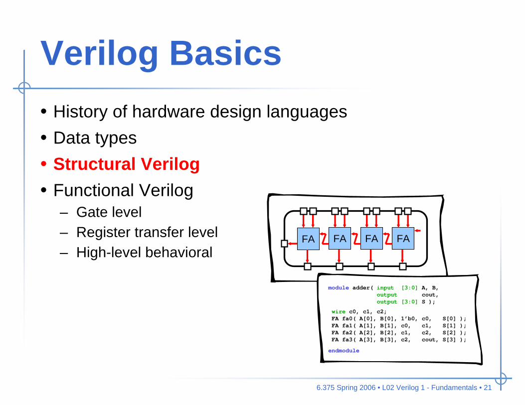
Verilog Fundamentals• History of hardware design languages• Data types• Structural Verilog• Functional Verilog
– Gate level– Register transfer level– High-level behavioral
FA FA FA FA
module adder( input [3:0] A, B,output cout,output [3:0] S );
wire c0, c1, c2;FA fa0( A[0], B[0], 1’b0, c0, S[0] );FA fa1( A[1], B[1], c0, c1, S[1] );FA fa2( A[2], B[2], c1, c2, S[2] );FA fa3( A[3], B[3], c2, cout, S[3] );
endmodule

6.375 Spring 2006 • L02 Verilog 1 - Fundamentals • 9
Originally designers used manual translation + bread boards for verification
BehavioralAlgorithm
RegisterTransfer Level
Gate Level
Manual
Manual
Manual
TestResults
BreadBoard
Number of Gatesin Design
10
102
103
104
105
106
107
6.375 Spring 2006 • L02 Verilog 1 - Fundamentals • 10
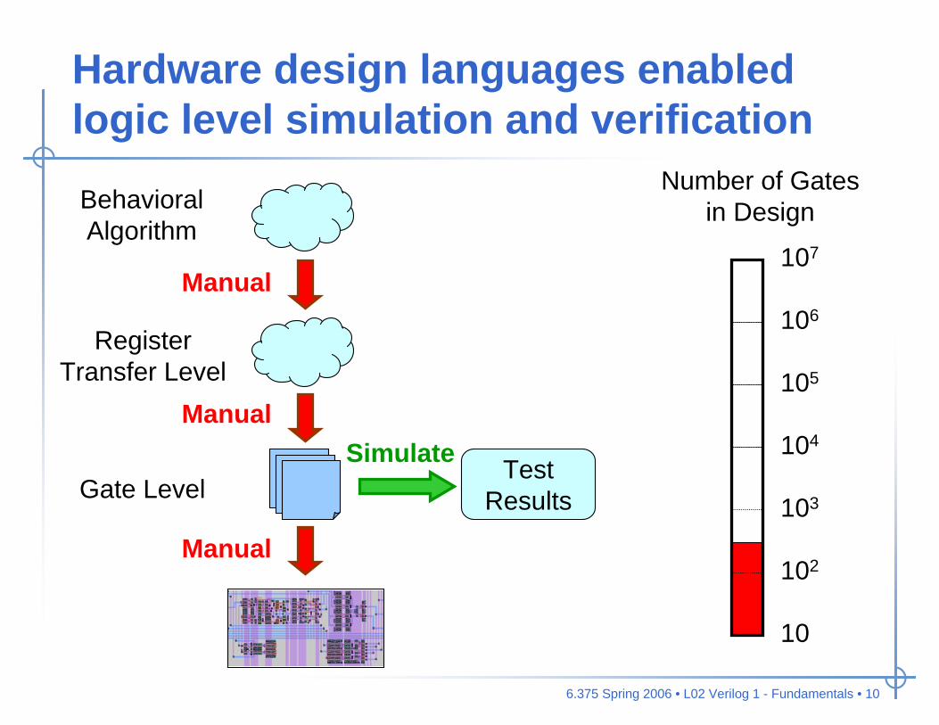
Hardware design languages enabled logic level simulation and verification
BehavioralAlgorithm
RegisterTransfer Level
Gate Level
Manual
Manual
Manual
TestResults
Simulate
Number of Gatesin Design
10
102
103
104
105
106
107
6.375 Spring 2006 • L02 Verilog 1 - Fundamentals • 11
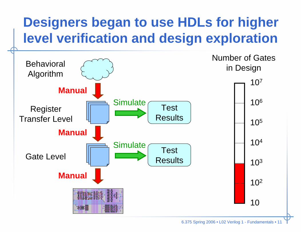
Designers began to use HDLs for higher level verification and design exploration
BehavioralAlgorithm
RegisterTransfer Level
Gate Level
Manual
Manual
Manual
TestResults
Simulate
TestResults
Simulate
Number of Gatesin Design
10
102
103
104
105
106
107

6.375 Spring 2006 • L02 Verilog 1 - Fundamentals • 12
HDL behavioral models act as a precise and executable specification
BehavioralAlgorithm
RegisterTransfer Level
Gate Level
Manual
Manual
Manual
TestResults
Simulate
TestResults
Simulate
TestResults
Simulate Number of Gatesin Design
10
102
103
104
105
106
107

6.375 Spring 2006 • L02 Verilog 1 - Fundamentals • 13
Once designs were written in HDLs tools could be used for automatic translation
BehavioralAlgorithm
RegisterTransfer Level
Gate Level
Manual
Manual
Auto Place + Route
TestResults
Simulate
TestResults
Simulate
TestResults
Simulate Number of Gatesin Design
10
102
103
104
105
106
107

6.375 Spring 2006 • L02 Verilog 1 - Fundamentals • 14
Once designs were written in HDLs tools could be used for automatic translation
BehavioralAlgorithm
RegisterTransfer Level
Gate Level
Manual
Logic Synthesis
Auto Place + Route
TestResults
Simulate
TestResults
Simulate
TestResults
Simulate Number of Gatesin Design
10
102
103
104
105
106
107

6.375 Spring 2006 • L02 Verilog 1 - Fundamentals • 15
Guarded atomic actions can help us to efficiently raise the abstraction level
BehavioralAlgorithm
RegisterTransfer Level
Gate Level
Logic Synthesis
TestResults
Simulate
TestResults
Simulate
TestResults
Simulate
Guarded Atomic Actions
Action Compiler
Manual
TestResults
Simulate
Number of Gatesin Design
10
102
103
104
105
106
107
6.375 Spring 2006 • L02 Verilog 1 - Fundamentals • 16
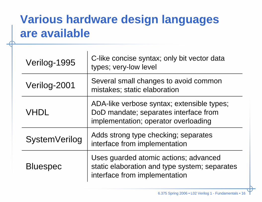
Various hardware design languages are available
Adds strong type checking; separates interface from implementationSystemVerilog
Uses guarded atomic actions; advanced static elaboration and type system; separates interface from implementation
Bluespec
ADA-like verbose syntax; extensible types; DoD mandate; separates interface from implementation; operator overloading
VHDL
Several small changes to avoid common mistakes; static elaborationVerilog-2001
C-like concise syntax; only bit vector data types; very-low levelVerilog-1995

6.375 Spring 2006 • L02 Verilog 1 - Fundamentals • 17
Verilog Fundamentals• History of hardware design languages• Data types• Structural Verilog• Functional Verilog
– Gate level– Register transfer level– High-level behavioral
FA FA FA FA
module adder( input [3:0] A, B,output cout,output [3:0] S );
wire c0, c1, c2;FA fa0( A[0], B[0], 1’b0, c0, S[0] );FA fa1( A[1], B[1], c0, c1, S[1] );FA fa2( A[2], B[2], c1, c2, S[2] );FA fa3( A[3], B[3], c2, cout, S[3] );
endmodule

6.375 Spring 2006 • L02 Verilog 1 - Fundamentals • 18
Primary Verilog data type is a bit-vector where bits can take on one of four values
High impedance, floatingZUnknown logic valueXLogic one1Logic zero0MeaningValue
An X bit might be a 0, 1, Z, or in transition. We can set bits to be X in situations where we don’t care what the value is. This can help catch bugs and
improve synthesis quality.
6.375 Spring 2006 • L02 Verilog 1 - Fundamentals • 19
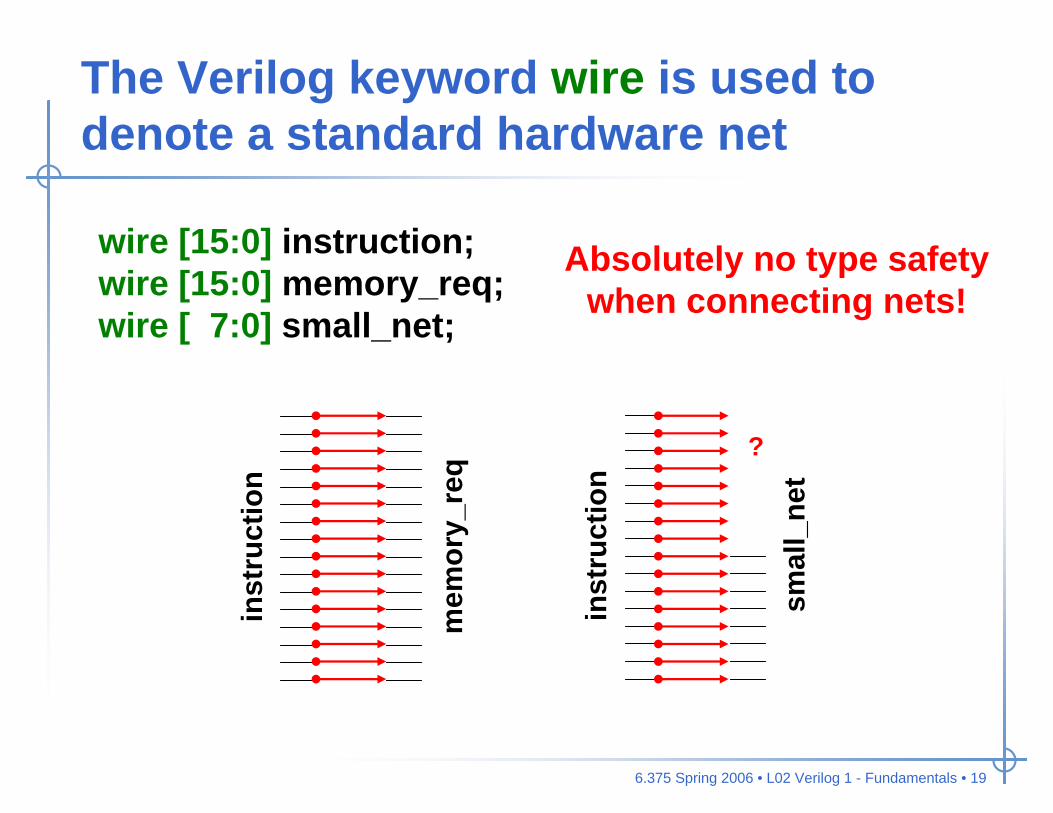
The Verilog keyword wire is used to denote a standard hardware net
wire [15:0] instruction;wire [15:0] memory_req;wire [ 7:0] small_net;
inst
ruct
ion
mem
ory_
req
inst
ruct
ion
smal
l_ne
t
?
Absolutely no type safety when connecting nets!

6.375 Spring 2006 • L02 Verilog 1 - Fundamentals • 20
Verilog includes ways to specify bit literals in various bases
• Binary literals– 8’b0000_0000– 8’b0xx0_1xx1
• Hexadecimal literals– 32’h0a34_def1– 16’haxxx
• Decimal literals– 32’d42
4’b10_11Underscores are ignored
Base format(d,b,o,h)
Decimal number representing size in bits
We’ll learn how to actually assign literals to
nets a little later
6.375 Spring 2006 • L02 Verilog 1 - Fundamentals • 21
Verilog Basics• History of hardware design languages• Data types• Structural Verilog• Functional Verilog
– Gate level– Register transfer level– High-level behavioral
FA FA FA FA
module adder( input [3:0] A, B,output cout,output [3:0] S );
wire c0, c1, c2;FA fa0( A[0], B[0], 1’b0, c0, S[0] );FA fa1( A[1], B[1], c0, c1, S[1] );FA fa2( A[2], B[2], c1, c2, S[2] );FA fa3( A[3], B[3], c2, cout, S[3] );
endmodule
6.375 Spring 2006 • L02 Verilog 1 - Fundamentals • 22
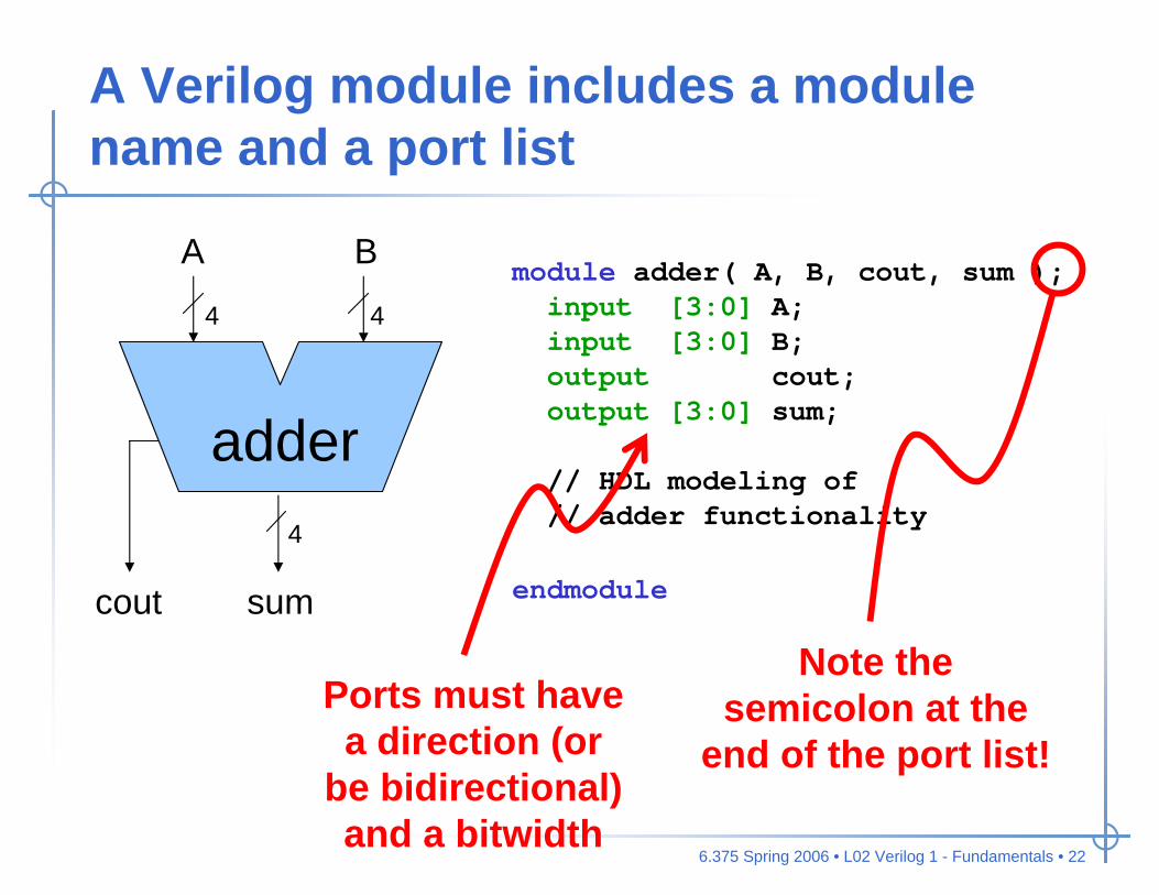
A Verilog module includes a module name and a port list
adder
A B
sumcout
module adder( A, B, cout, sum );input [3:0] A;input [3:0] B;output cout;output [3:0] sum;
// HDL modeling of // adder functionality
endmodule
Note the semicolon at the
end of the port list!Ports must have
a direction (or be bidirectional) and a bitwidth
4 4
4

6.375 Spring 2006 • L02 Verilog 1 - Fundamentals • 23
Traditional Verilog-1995 Syntax
module adder( A, B, cout, sum );input [3:0] A;input [3:0] B;output cout;output [3:0] sum;
ANSI C Style Verilog-2001 Syntax
module adder( input [3:0] A,input [3:0] B,output cout,output [3:0] sum );
A Verilog module includes a module name and a port list
adder
A B
sumcout
4 4
4

6.375 Spring 2006 • L02 Verilog 1 - Fundamentals • 24
A module can instantiate other modules creating a module hierarchy
module FA( input a, b, cinoutput cout, sum );
// HDL modeling of 1 bit// adder functionality
endmodule
FA
ba
c
cin
cout
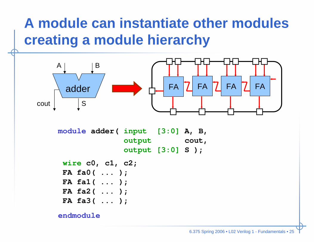
6.375 Spring 2006 • L02 Verilog 1 - Fundamentals • 25
A module can instantiate other modules creating a module hierarchy
adder
A B
Scout
FA FA FA FA
module adder( input [3:0] A, B,output cout,output [3:0] S );
wire c0, c1, c2;FA fa0( ... );FA fa1( ... );FA fa2( ... );FA fa3( ... );
endmodule
6.375 Spring 2006 • L02 Verilog 1 - Fundamentals • 26
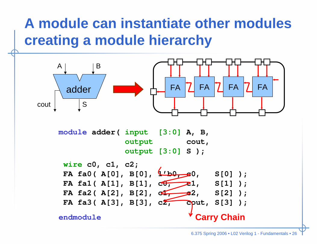
A module can instantiate other modules creating a module hierarchy
adder
A B
Scout
FA FA FA FA
module adder( input [3:0] A, B,output cout,output [3:0] S );
wire c0, c1, c2;FA fa0( A[0], B[0], 1’b0, c0, S[0] );FA fa1( A[1], B[1], c0, c1, S[1] );FA fa2( A[2], B[2], c1, c2, S[2] );FA fa3( A[3], B[3], c2, cout, S[3] );
endmodule Carry Chain

6.375 Spring 2006 • L02 Verilog 1 - Fundamentals • 27
Verilog supports connecting ports by position and by name
Connecting ports by ordered listFA fa0( A[0], B[0], 1’b0, c0, S[0] );
Connecting ports by name (compact)FA fa0( .a(A[0]), .b(B[0]),
.cin(1’b0), .cout(c0), .sum(S[0]) );
Connecting ports by nameFA fa0( .a (A[0]), .b (B[0]), .cin (1’b0), .cout (c0), .sum (S[0])
);
For all but the smallest modules, connecting ports by name yields clearer and
less buggy code.
6.375 Spring 2006 • L02 Verilog 1 - Fundamentals • 28
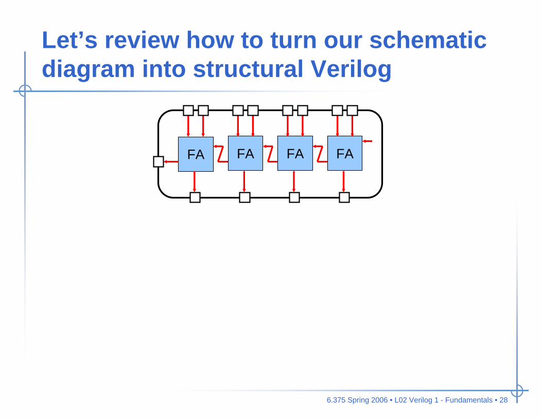
Let’s review how to turn our schematic diagram into structural Verilog
FA FA FA FA

6.375 Spring 2006 • L02 Verilog 1 - Fundamentals • 29
module adder( ... );
endmodule
module adder( input [3:0] A, B,output cout,output [3:0] S );
endmodule
Let’s review how to turn our schematic diagram into structural Verilog
module adder( input [3:0] A, B,output cout,output [3:0] S );
FA fa0( ... );FA fa1( ... );FA fa2( ... );FA fa3( ... );
endmodule
FA FA FA FA
module adder( input [3:0] A, B,output cout,output [3:0] S );
wire c0, c1, c2;FA fa0( A[0], B[0], 1’b0, c0, S[0] );FA fa1( A[1], B[1], c0, c1, S[1] );FA fa2( A[2], B[2], c1, c2, S[2] );FA fa3( A[3], B[3], c2, cout, S[3] );
endmodule
6.375 Spring 2006 • L02 Verilog 1 - Fundamentals • 30
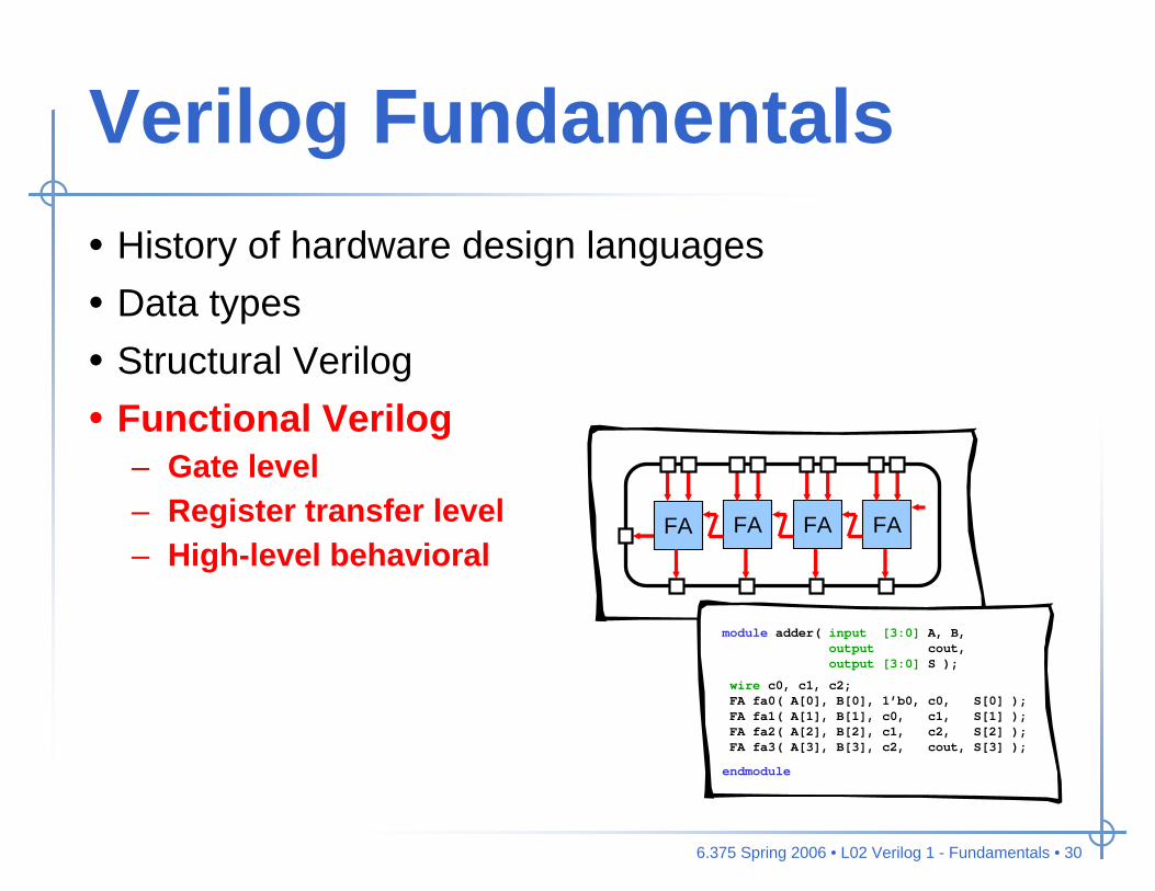
Verilog Fundamentals• History of hardware design languages• Data types• Structural Verilog• Functional Verilog
– Gate level– Register transfer level– High-level behavioral
FA FA FA FA
module adder( input [3:0] A, B,output cout,output [3:0] S );
wire c0, c1, c2;FA fa0( A[0], B[0], 1’b0, c0, S[0] );FA fa1( A[1], B[1], c0, c1, S[1] );FA fa2( A[2], B[2], c1, c2, S[2] );FA fa3( A[3], B[3], c2, cout, S[3] );
endmodule

6.375 Spring 2006 • L02 Verilog 1 - Fundamentals • 31
Functional Verilog can roughly be divided into three abstraction levels
BehavioralAlgorithm
RegisterTransfer Level
Gate Level
Manual
Logic Synthesis
Auto Place + Route
V
V
V Abstract algorithmic description
Describes how data flows between state elements for each cycle
Low-level netlist of primitive gates

6.375 Spring 2006 • L02 Verilog 1 - Fundamentals • 32
module mux4( input a, b, c, d, input [1:0] sel, output out );
wire [1:0] sel_b;not not0( sel_b[0], sel[0] );not not1( sel_b[1], sel[1] );
wire n0, n1, n2, n3;and and0( n0, c, sel[1] );and and1( n1, a, sel_b[1] );and and2( n2, d, sel[1] );and and3( n3, b, sel_b[1] );
wire x0, x1;nor nor0( x0, n0, n1 );nor nor1( x1, n2, n3 );
wire y0, y1;or or0( y0, x0, sel[0] );or or1( y1, x1, sel_b[0] );nand nand0( out, y0, y1 );
endmodule
Gate-level Verilog uses structural Verilog to connect primitive gates
sel[0]sel[1]cadb
out

6.375 Spring 2006 • L02 Verilog 1 - Fundamentals • 33
Continuous assignment statementsassign one net to another or to a literal
Explicit continuous assignment
wire [15:0] netA;wire [15:0] netB;
assign netA = 16’h3333;assign netB = netA;
Implicit continuous assignment
wire [15:0] netA = 16’h3333;wire [15:0] netB = netA;

6.375 Spring 2006 • L02 Verilog 1 - Fundamentals • 34
module mux4( input a, b, c, dinput [1:0] sel,output out );
wire out, t0, t1;assign out = ~( (t0 | sel[0]) & (t1 | ~sel[0]) );assign t1 = ~( (sel[1] & d) | (~sel[1] & b) );assign t0 = ~( (sel[1] & c) | (~sel[1] & a) );
endmodule
Using continuous assignments to implement an RTL four input multiplexer
module mux4( input a, b, c, dinput [1:0] sel,output out );
wire out, t0, t1;assign t0 = ~( (sel[1] & c) | (~sel[1] & a) );assign t1 = ~( (sel[1] & d) | (~sel[1] & b) );assign out = ~( (t0 | sel[0]) & (t1 | ~sel[0]) );
endmodule
The order of these continuous assignment statements does not matter.
They essentially happen in parallel!
6.375 Spring 2006 • L02 Verilog 1 - Fundamentals • 35
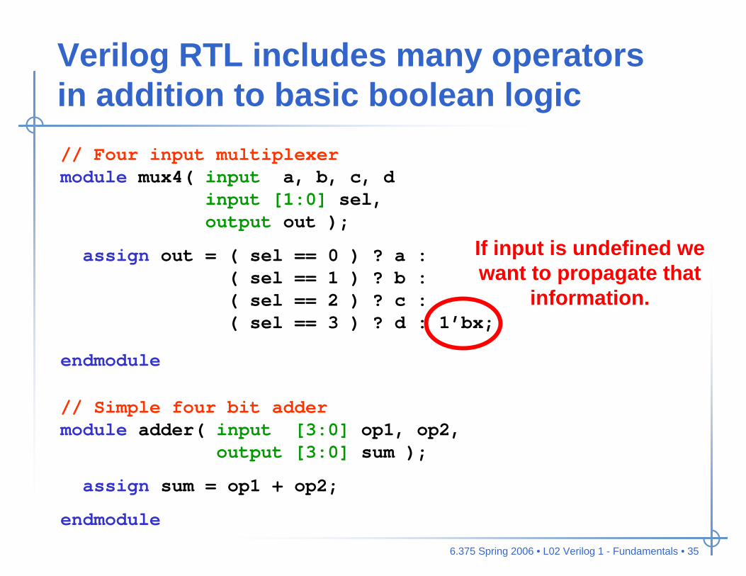
Verilog RTL includes many operators in addition to basic boolean logic// Four input multiplexermodule mux4( input a, b, c, d
input [1:0] sel,output out );
assign out = ( sel == 0 ) ? a :( sel == 1 ) ? b :( sel == 2 ) ? c :( sel == 3 ) ? d : 1’bx;
endmodule
// Simple four bit addermodule adder( input [3:0] op1, op2,
output [3:0] sum );
assign sum = op1 + op2;
endmodule
If input is undefined we want to propagate that
information.

6.375 Spring 2006 • L02 Verilog 1 - Fundamentals • 36
Verilog RTL operators
~ & | ^ ^~Bitwise== != === !===Equality> < >= <=Relational! && ||Logical+ - * / % **Arithmetic
wire [ 3:0] net1 = 4’b00xx;wire [ 3:0] net2 = 4’b1110;wire [11:0] net3 = { 4’b0, net1, net2 };
& ~& | ~| ^ ^~Reduction>> << >>> <<<Shift{ }Concatenation?:Conditional
Avoid ( / % ** ) since the usually synthesize poorly
wire equal = ( net3 === 12’b0000_1110_00xx );
6.375 Spring 2006 • L02 Verilog 1 - Fundamentals • 37
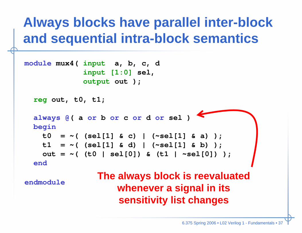
Always blocks have parallel inter-block and sequential intra-block semantics module mux4( input a, b, c, d
input [1:0] sel,output out );
reg out, t0, t1;
always @( a or b or c or d or sel )begint0 = ~( (sel[1] & c) | (~sel[1] & a) );t1 = ~( (sel[1] & d) | (~sel[1] & b) );out = ~( (t0 | sel[0]) & (t1 | ~sel[0]) );
end
endmoduleThe always block is reevaluated
whenever a signal in its sensitivity list changes

6.375 Spring 2006 • L02 Verilog 1 - Fundamentals • 38
Always blocks have parallel inter-block and sequential intra-block semantics module mux4( input a, b, c, d
input [1:0] sel,output out );
reg out, t0, t1;
always @( a or b or c or d or sel )begint0 = ~( (sel[1] & c) | (~sel[1] & a) );t1 = ~( (sel[1] & d) | (~sel[1] & b) );out = ~( (t0 | sel[0]) & (t1 | ~sel[0]) );
end
endmoduleThe order of these procedural
assignment statements does matter.They essentially happen in sequentially!

6.375 Spring 2006 • L02 Verilog 1 - Fundamentals • 39
Always blocks have parallel inter-block and sequential intra-block semantics module mux4( input a, b, c, d
input [1:0] sel,output out );
reg out, t0, t1;
always @( a or b or c or d or sel )begint0 = ~( (sel[1] & c) | (~sel[1] & a) );t1 = ~( (sel[1] & d) | (~sel[1] & b) );out = ~( (t0 | sel[0]) & (t1 | ~sel[0]) );
end
endmoduleLHS of procedural assignments must be declared as a reg type. Verilog reg is not
necessarily a hardware register!

6.375 Spring 2006 • L02 Verilog 1 - Fundamentals • 40
Always blocks have parallel inter-block and sequential intra-block semantics module mux4( input a, b, c, d
input [1:0] sel,output out );
reg out, t0, t1;
always @( a or b or c or d or sel )begint0 = ~( (sel[1] & c) | (~sel[1] & a) );t1 = ~( (sel[1] & d) | (~sel[1] & b) );out = ~( (t0 | sel[0]) & (t1 | ~sel[0]) );
end
endmoduleWhat happens if we accidentally
forget a signal on the sensitivity list?

6.375 Spring 2006 • L02 Verilog 1 - Fundamentals • 41
Always blocks have parallel inter-block and sequential intra-block semantics module mux4( input a, b, c, d
input [1:0] sel,output out );
reg out, t0, t1;
always @( * )begint0 = ~( (sel[1] & c) | (~sel[1] & a) );t1 = ~( (sel[1] & d) | (~sel[1] & b) );out = ~( (t0 | sel[0]) & (t1 | ~sel[0]) );
end
endmoduleVerilog-2001 provides special syntax to automatically create a sensitivity list for
all signals read in the always block

6.375 Spring 2006 • L02 Verilog 1 - Fundamentals • 42
Continuous and procedural assignment statements are very differentContinuous assignments are for naming and thus we cannot have multiple assignments for the same wirewire out, t0, t1;assign t0 = ~( (sel[1] & c) | (~sel[1] & a) );assign t1 = ~( (sel[1] & d) | (~sel[1] & b) );assign out = ~( (t0 | sel[0]) & (t1 | ~sel[0]) );
Procedural assignments hold a value semantically, but it is important to distinguish this from hardware statereg out, t0, t1, temp;always @( * )begintemp = ~( (sel[1] & c) | (~sel[1] & a) );t0 = temp;temp = ~( (sel[1] & d) | (~sel[1] & b) );t1 = temp;out = ~( (t0 | sel[0]) & (t1 | ~sel[0]) );
end

6.375 Spring 2006 • L02 Verilog 1 - Fundamentals • 43
Always blocks can contain more advanced control constructs
module mux4( input a, b, c, dinput [1:0] sel,output out );
reg out;
always @( * )beginif ( sel == 2’d0 )out = a;
else if ( sel == 2’d1 )out = b
else if ( sel == 2’d2 )out = c
else if ( sel == 2’d3 )out = d
elseout = 1’bx;
end
endmodule
module mux4( input a, b, c, dinput [1:0] sel,output out );
reg out;
always @( * )begincase ( sel )2’d0 : out = a;2’d1 : out = b;2’d2 : out = c;2’d3 : out = d;default : out = 1’bx;
endcaseend
endmodule
6.375 Spring 2006 • L02 Verilog 1 - Fundamentals • 44
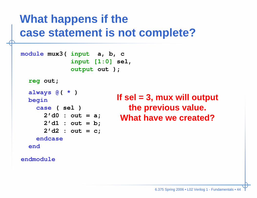
What happens if the case statement is not complete?module mux3( input a, b, c
input [1:0] sel,output out );
reg out;
always @( * )begincase ( sel )2’d0 : out = a;2’d1 : out = b;2’d2 : out = c;
endcaseend
endmodule
If sel = 3, mux will outputthe previous value.
What have we created?

6.375 Spring 2006 • L02 Verilog 1 - Fundamentals • 45
What happens if the case statement is not complete?module mux3( input a, b, c
input [1:0] sel,output out );
reg out;
always @( * )begincase ( sel )2’d0 : out = a;2’d1 : out = b;2’d2 : out = c;default : out = 1’bx;
endcaseend
endmodule
We can prevent creating state with a default statement

6.375 Spring 2006 • L02 Verilog 1 - Fundamentals • 46
So is this how we make latches and flip-flops?
module latch( input clk, input d, output reg q
);
always @( clk )beginif ( clk )d = q;
end
endmodule
module flipflop( input clk, input d, output q
);
always @( posedge clk )begind = q;
end
endmodule Edge-triggered always block

6.375 Spring 2006 • L02 Verilog 1 - Fundamentals • 47
To understand why we need to know more about Verilog execution semanticswire A_in, B_in, C_in;reg A_out, B_out, C_out;
always @( posedge clk )A_out = A_in;
assign B_in = A_out + 1;
always @( posedge clk )B_out = B_in;
assign C_in = B_out + 1;
always @( posedge clk )C_out = C_in;
+1
A
+1
B C

6.375 Spring 2006 • L02 Verilog 1 - Fundamentals • 48
To understand why we need to know more about Verilog execution semanticswire A_in, B_in, C_in;reg A_out, B_out, C_out;
always @( posedge clk )A_out = A_in;
assign B_in = A_out + 1;
always @( posedge clk )B_out = B_in;
assign C_in = B_out + 1;
always @( posedge clk )C_out = C_in;
Active Event Queue
A
1
B
2
C
On clock edge all those events which are sensitive to the
clock are added to the active event queue in
any order!
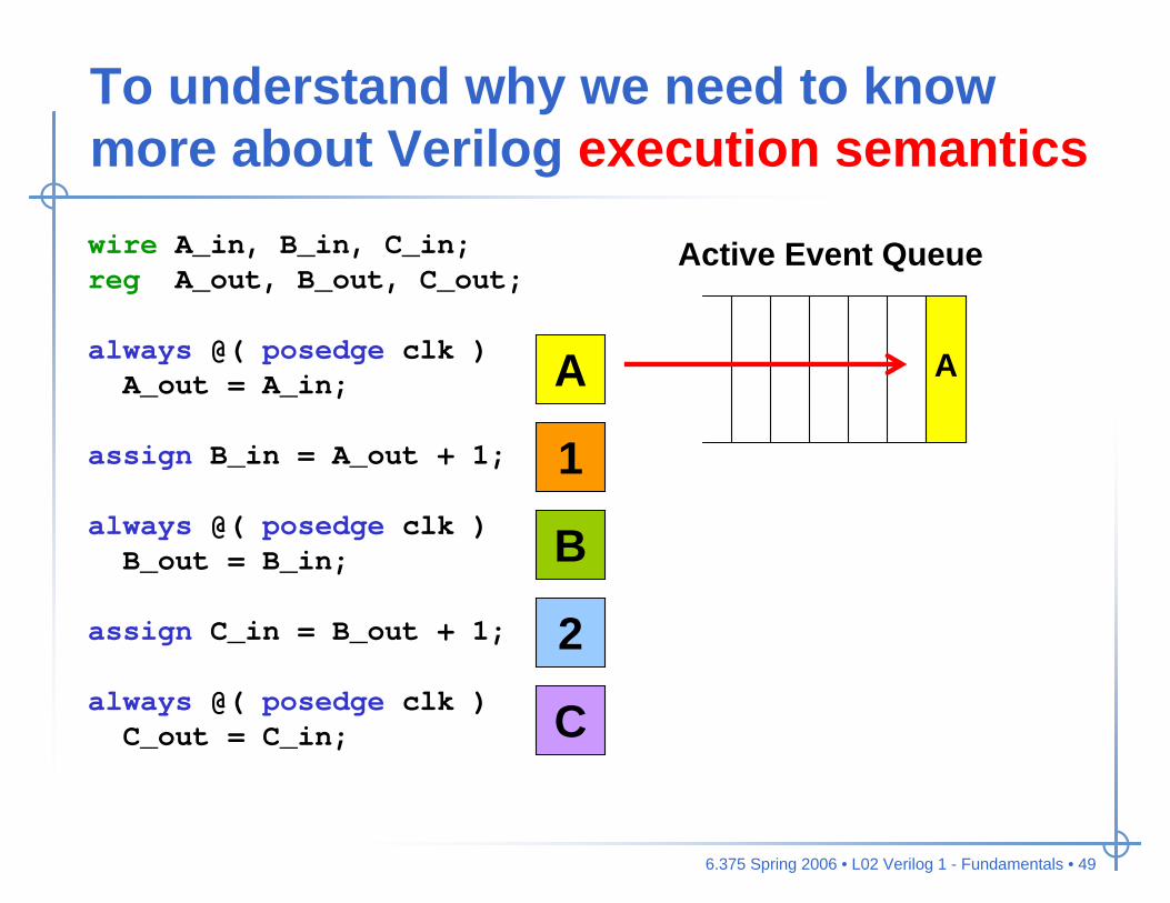
6.375 Spring 2006 • L02 Verilog 1 - Fundamentals • 49
To understand why we need to know more about Verilog execution semanticswire A_in, B_in, C_in;reg A_out, B_out, C_out;
always @( posedge clk )A_out = A_in;
assign B_in = A_out + 1;
always @( posedge clk )B_out = B_in;
assign C_in = B_out + 1;
always @( posedge clk )C_out = C_in;
Active Event Queue
AA
1
B
2
C
6.375 Spring 2006 • L02 Verilog 1 - Fundamentals • 50
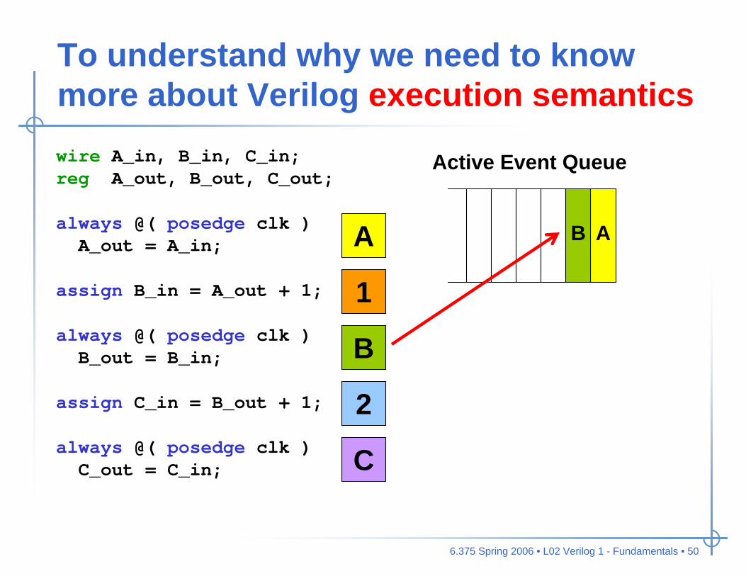
To understand why we need to know more about Verilog execution semanticswire A_in, B_in, C_in;reg A_out, B_out, C_out;
always @( posedge clk )A_out = A_in;
assign B_in = A_out + 1;
always @( posedge clk )B_out = B_in;
assign C_in = B_out + 1;
always @( posedge clk )C_out = C_in;
Active Event Queue
AA
1
B
2
C
B

6.375 Spring 2006 • L02 Verilog 1 - Fundamentals • 51
To understand why we need to know more about Verilog execution semanticswire A_in, B_in, C_in;reg A_out, B_out, C_out;
always @( posedge clk )A_out = A_in;
assign B_in = A_out + 1;
always @( posedge clk )B_out = B_in;
assign C_in = B_out + 1;
always @( posedge clk )C_out = C_in;
Active Event Queue
AA
1
B
2
C
BC
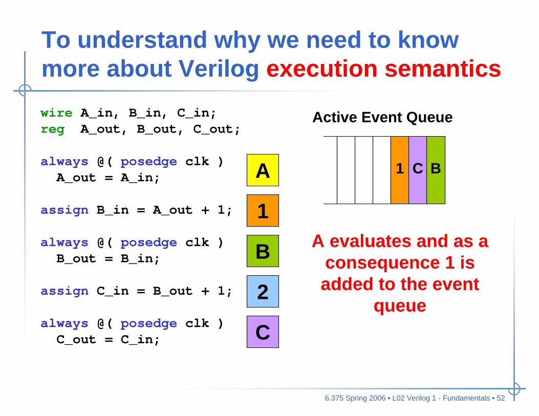
6.375 Spring 2006 • L02 Verilog 1 - Fundamentals • 52
To understand why we need to know more about Verilog execution semanticswire A_in, B_in, C_in;reg A_out, B_out, C_out;
always @( posedge clk )A_out = A_in;
assign B_in = A_out + 1;
always @( posedge clk )B_out = B_in;
assign C_in = B_out + 1;
always @( posedge clk )C_out = C_in;
Active Event Queue
AA
1
B
2
C
BC
A evaluates and as a consequence 1 is added to the event
queue
BC1
6.375 Spring 2006 • L02 Verilog 1 - Fundamentals • 53
To understand why we need to know more about Verilog execution semanticswire A_in, B_in, C_in;reg A_out, B_out, C_out;
always @( posedge clk )A_out = A_in;
assign B_in = A_out + 1;
always @( posedge clk )B_out = B_in;
assign C_in = B_out + 1;
always @( posedge clk )C_out = C_in;
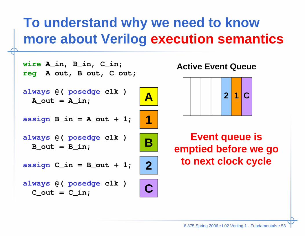
Active Event Queue
A
1
B
2
C
B evaluates and as a consequence 2 is added to the event
queue
BC1 C12
Event queue is emptied before we go
to next clock cycle
6.375 Spring 2006 • L02 Verilog 1 - Fundamentals • 54
To understand why we need to know more about Verilog execution semanticswire A_in, B_in, C_in;reg A_out, B_out, C_out;
always @( posedge clk )A_out = A_in;
assign B_in = A_out + 1;
always @( posedge clk )B_out = B_in;
assign C_in = B_out + 1;
always @( posedge clk )C_out = C_in;
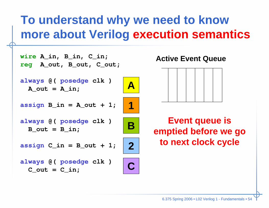
Active Event Queue
A
1
B
2
C
Event queue is emptied before we go
to next clock cycle

6.375 Spring 2006 • L02 Verilog 1 - Fundamentals • 55
To understand why we need to know more about Verilog execution semanticswire A_in, B_in, C_in;reg A_out, B_out, C_out;
always @( posedge clk )A_out = A_in;
assign B_in = A_out + 1;
always @( posedge clk )B_out = B_in;
assign C_in = B_out + 1;
always @( posedge clk )C_out = C_in;
A
1
B
2
C
+1
A
+1
B C
+1 +1

6.375 Spring 2006 • L02 Verilog 1 - Fundamentals • 56
Non-blocking procedural assignments add an extra event queuewire A_in, B_in, C_in;reg A_out, B_out, C_out;
always @( posedge clk )A_out <= A_in;
assign B_in = A_out + 1;
always @( posedge clk )B_out <= B_in;
assign C_in = B_out + 1;
always @( posedge clk )C_out <= C_in;
Active Event Queue
A
1
B
2
C
Non-Blocking Queue
AR
BR
CR12
AL
BL
CL
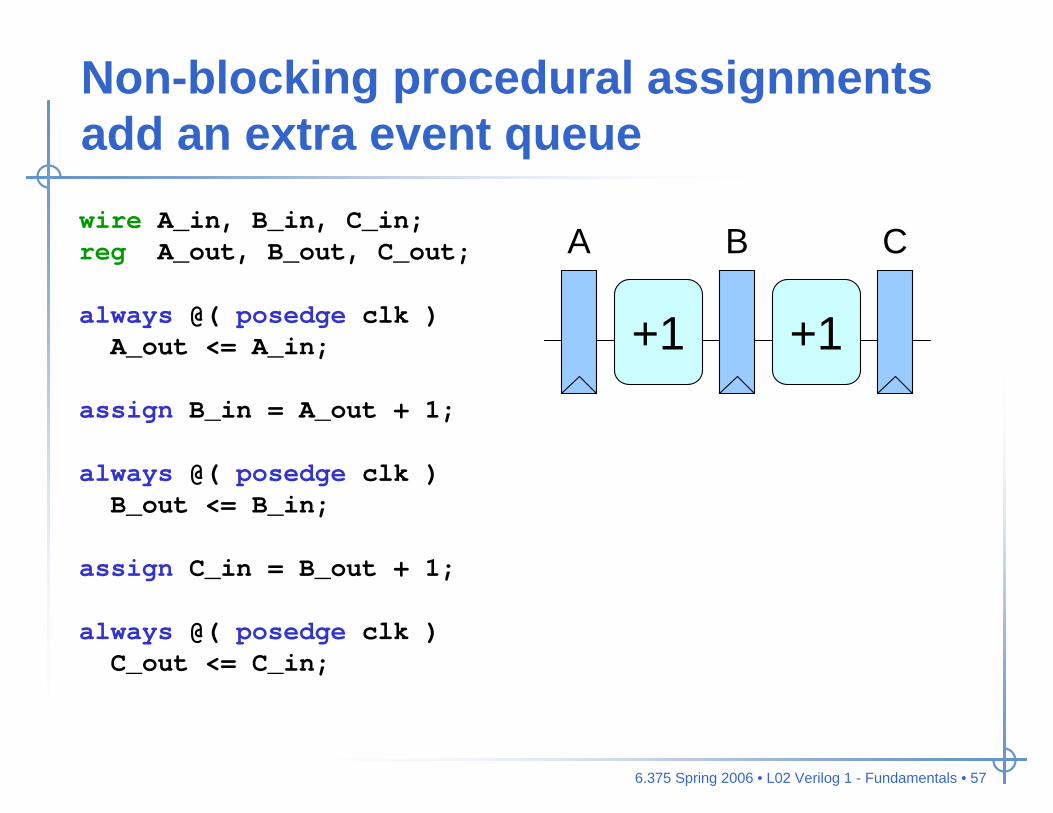
6.375 Spring 2006 • L02 Verilog 1 - Fundamentals • 57
Non-blocking procedural assignments add an extra event queuewire A_in, B_in, C_in;reg A_out, B_out, C_out;
always @( posedge clk )A_out <= A_in;
assign B_in = A_out + 1;
always @( posedge clk )B_out <= B_in;
assign C_in = B_out + 1;
always @( posedge clk )C_out <= C_in;
+1
A
+1
B C
6.375 Spring 2006 • L02 Verilog 1 - Fundamentals • 58
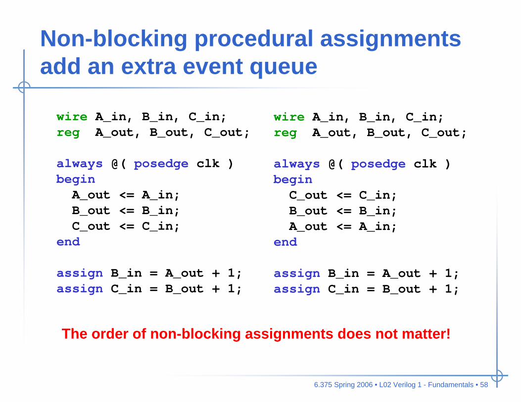
Non-blocking procedural assignments add an extra event queue
wire A_in, B_in, C_in;reg A_out, B_out, C_out;
always @( posedge clk )beginA_out <= A_in;B_out <= B_in;C_out <= C_in;
end
assign B_in = A_out + 1;assign C_in = B_out + 1;
wire A_in, B_in, C_in;reg A_out, B_out, C_out;
always @( posedge clk )beginC_out <= C_in;B_out <= B_in;A_out <= A_in;
end
assign B_in = A_out + 1;assign C_in = B_out + 1;
The order of non-blocking assignments does not matter!

6.375 Spring 2006 • L02 Verilog 1 - Fundamentals • 59
Common patterns for latch and flip-flop inference
always @( clk )beginif ( clk )D <= Q;
end
always @( posedge clk )beginD <= Q;
end
always @( posedge clk )beginif ( enable )D <= Q;
end
D Q Xnext_Xclk
D Q Xnext_Xclk
D Q Xnext_Xclk
enable

6.375 Spring 2006 • L02 Verilog 1 - Fundamentals • 60
Six guidelines for using blocking and non-blocking assignment statments
1. Flip-flops should use non-blocking
2. Latches should use non-blocking
3. Combinational logic should use blocking
4. Do not mix combinational and sequential logic in the same always block
5. Do not assign to the same variable from more than one always block

6.375 Spring 2006 • L02 Verilog 1 - Fundamentals • 61
Behavioral Verilog is used to model the abstract function of a hardware module
• Characterized by heavy use of sequential blocking statements in large always blocks
• Many constructs are not synthesizable but can be useful for behavioral modeling– Data dependent for and while loops– Additional behavioral datatypes : integer, real– Magic initialization blocks : initial– Magic delay statements: #<delay>

6.375 Spring 2006 • L02 Verilog 1 - Fundamentals • 62
Verilog can be used to model the high-level behavior of a hardware blockmodule factorial( input [ 7:0] in, output reg [15:0] out );
integer num_calls;initial num_calls = 0;
integer multiplier;integer result; always @(*)begin
multiplier = in;result = 1;while ( multiplier > 0 )beginresult = result * multiplier;multiplier = multiplier - 1;
end
out = result;num_calls = num_calls + 1;
end
endmodule
Data dependent while loop
Variables of type integer
Initial statement
6.375 Spring 2006 • L02 Verilog 1 - Fundamentals • 63
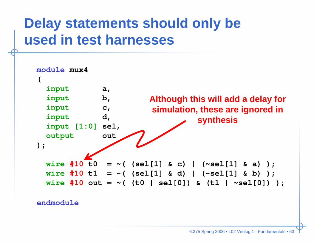
Delay statements should only be used in test harnesses
module mux4( input a, input b, input c, input d, input [1:0] sel,output out
);
wire #10 t0 = ~( (sel[1] & c) | (~sel[1] & a) );wire #10 t1 = ~( (sel[1] & d) | (~sel[1] & b) );wire #10 out = ~( (t0 | sel[0]) & (t1 | ~sel[0]) );
endmodule
Although this will add a delay for simulation, these are ignored in
synthesis
6.375 Spring 2006 • L02 Verilog 1 - Fundamentals • 64
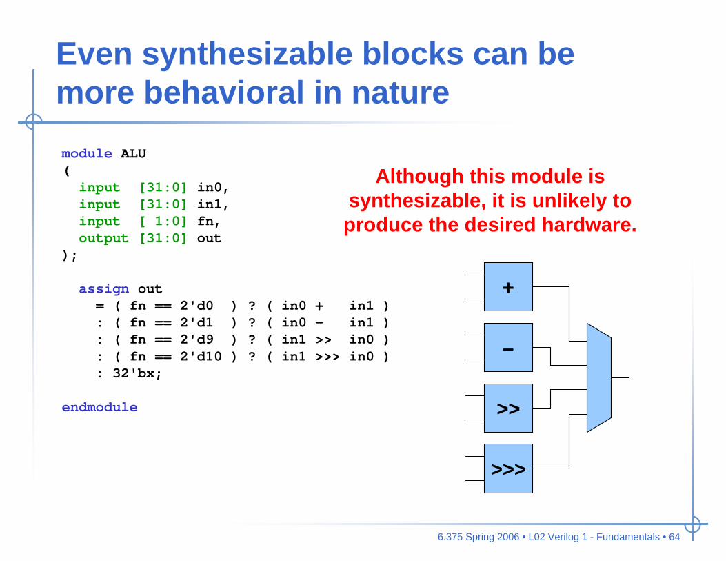
Even synthesizable blocks can be more behavioral in naturemodule ALU(input [31:0] in0,input [31:0] in1,input [ 1:0] fn,output [31:0] out
);
assign out = ( fn == 2'd0 ) ? ( in0 + in1 ): ( fn == 2'd1 ) ? ( in0 - in1 ): ( fn == 2'd9 ) ? ( in1 >> in0 ): ( fn == 2'd10 ) ? ( in1 >>> in0 ): 32'bx;
endmodule
Although this module is synthesizable, it is unlikely to produce the desired hardware.
+
–
>>
>>>
6.375 Spring 2006 • L02 Verilog 1 - Fundamentals • 65
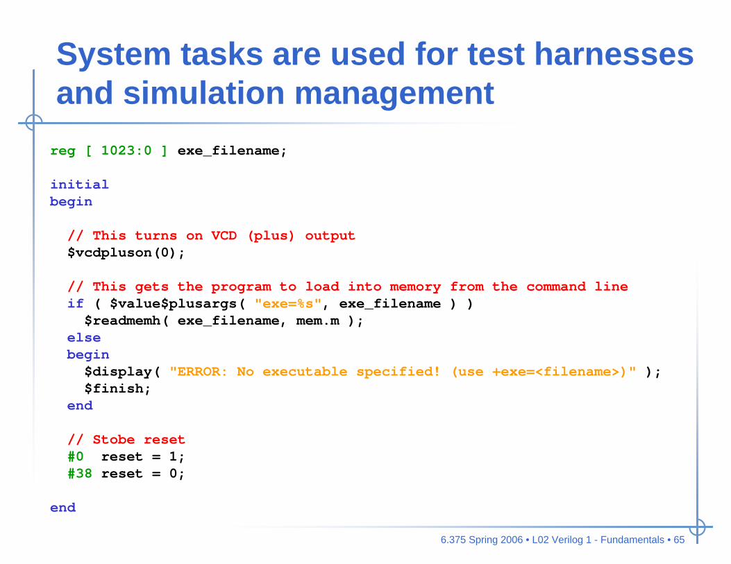
System tasks are used for test harnesses and simulation managementreg [ 1023:0 ] exe_filename;
initialbegin
// This turns on VCD (plus) output$vcdpluson(0);
// This gets the program to load into memory from the command lineif ( $value$plusargs( "exe=%s", exe_filename ) )$readmemh( exe_filename, mem.m );
elsebegin$display( "ERROR: No executable specified! (use +exe=<filename>)" );$finish;
end
// Stobe reset#0 reset = 1;#38 reset = 0;
end

6.375 Spring 2006 • L02 Verilog 1 - Fundamentals • 66
Which abstraction is the right one?
Designers usually use a mix of all three! Early on in the design process they might use mostly behavioral models. As the design is refined, the behavioral models begin to be replaced by dataflow models. Finally, the designers use automatic tools to synthesize a low-level gate-level model.
High-Level Behavioral
Register Transfer Level
Gate Level

6.375 Spring 2006 • L02 Verilog 1 - Fundamentals • 67
Take away points• Structural Verilog enables us to describe a hardware
schematic textually• Verilog can model hardware at three levels of abstraction:
gate level, register transfer level, and behavioral• Understanding the Verilog execution semantics is critical
for understanding blocking + non-blocking assignments• Designers must have the hardware they are trying to
create in mind when they write their Verilog
Next Lecture: We will use a simple SMIPS processor to illustrate many of concepts
introduced today.