departmentkgr.ac.in/beta/wp-content/uploads/2018/09/network-thoery.pdf · verification of...
TRANSCRIPT

NETWORKS LAB
Department of Electrical & Electronics Engineering
DEPARTMENT
OF
ELECTRICAL AND ELECTRONICS ENGINEERING
III B.TECH I SEMESTER
REGULATION/LAB CODE: R16/EE506PC
LABORATORY MANUAL
BASIC ELECTRICAL SIMULATION

NETWORKS LAB
Department of Electrical & Electronics Engineering

NETWORKS LAB
Department of Electrical & Electronics Engineering
DEPARTMENT VISION
To become a renowned department imparting both technical and non-technical skills to the students
by implementing new engineering pedagogy’s and research to produce competent new age electrical
engineers.
DEPARTMENT MISSION
To transform the students into motivated and knowledgeable new age electrical engineers.
To advance the quality of education to produce world class technocrats with an ability to adapt to
the academically challenging environment.
To provide a progressive environment for learning through organized teaching methodologies,
contemporary curriculum and research in the thrust areas of electrical engineering.

NETWORKS LAB
Department of Electrical & Electronics Engineering
Program Educational Objectives (PEO’s):
PEO 1: Apply knowledge and skills to provide solutions to Electrical and Electronics
Engineering problems in industry and governmental organizations or to enhance student learning
in educational institutions
PEO 2: Work as a team with a sense of ethics and professionalism, and communicate
effectively to manage cross-cultural and multidisciplinary teams
PEO 3: Update their knowledge continuously through lifelong learning that contributes to
personal, global and organizational growth

NETWORKS LAB
Department of Electrical & Electronics Engineering
Program Outcomes(PO’s):
A graduate of the Electrical and Electronics Engineering Program will demonstrate:
PO 1: Engineering knowledge: Apply the knowledge of mathematics, science, engineering
fundamentals and an engineering specialization to the solution of complex engineering problems.
PO 2: Problem analysis: Identify, formulate, review research literature, and analyze complex
engineering problems reaching substantiated conclusions using first principles of mathematics,
natural science and engineering sciences.
PO 3: Design/development of solutions: design solutions for complex engineering problems and
design system components or processes that meet the specified needs with appropriate
consideration for the public health and safety, and the cultural, societal and environmental
considerations.
PO 4: Conduct investigations of complex problems: use research based knowledge and research
methods including design of experiments, analysis and interpretation of data, and synthesis of the
information to provide valid conclusions.
PO 5: Modern tool usage: create, select and apply appropriate techniques, resources and modern
engineering and IT tools including prediction and modelling to complex engineering activities
with an understanding of the limitations.
PO 6: The engineer and society: apply reasoning informed by the contextual knowledge to assess
societal, health, safety, legal and cultural issues and the consequent responsibilities relevant to the
professional engineering practice.
PO 7: Environment sustainability: understand the impact of the professional engineering
solutions in the societal and environmental contexts, and demonstrate the knowledge of, and need
for sustainable development.
PO 8: Ethics: apply ethical principles and commit to professional ethics and responsibilities and
norms of the engineering practice.
PO 9: Individual and team work: function effectively as an individual and as a member or leader
in diverse teams, and in multidisciplinary settings.
PO 10: Communication: communicate effectively on complex engineering activities with the
engineering community and with society at large, such as, being able to comprehend and write

NETWORKS LAB
Department of Electrical & Electronics Engineering
effective reports and design documentation, make effective presentations, and give and receive
clear instructions.
PO 11: Project management and finance: demonstrate knowledge and understanding of the
engineering and management principles and apply these to one’s own work, as a member and
leader in a team, to manage projects and in multidisciplinary environments.
PO 12: Lifelong learning: recognize the need for, and have the preparation and ability to engage
in independent and lifelong learning in the broader context of technological change.

NETWORKS LAB
Department of Electrical & Electronics Engineering
Program Specific Outcomes(PSO’s):
PSO-1: Apply the engineering fundamental knowledge to identify, formulate, design and investigate
complex engineering problems of electric circuits, power electronics, electrical machines and power
systems and to succeed in competitive exams like GATE, IES, GRE, OEFL, GMAT, etc.
PSO-2: Apply appropriate techniques and modern engineering hardware and software tools in power
systems and power electronics to engage in life-long learning and to get an employment in the field of
Electrical and Electronics Engineering.
PSO-3: Understand the impact of engineering solutions in societal and environmental context, commit
to professional ethics and communicate effectively.

NETWORKS LAB
Department of Electrical & Electronics Engineering
Course Outcomes (CO’s):
Upon completion of this course, the student will be able to:
(CO1) Analyze complex DC and AC linear circuits
(CO2) Apply concepts of electrical circuits across engineering
(CO3) Evaluate response in a given network by using theorems
(CO4) Analyze a given network by applying various Network Theorems
.

NETWORKS LAB
Department of Electrical & Electronics Engineering

NETWORKS LAB
Department of Electrical & Electronics Engineering
NETWORKS LAB EE307ES
B.Tech. II Year I Sem. L T P C
0 0 3 2
Note: Minimum 10 experiments should be conducted.
Experiments are conducted by using trainer kits, bread boards and multimeters. The following experiments are required to be conducted compulsory experiments:
1. Verification of Thevenin’s and Norton’s Theorems
2. Verification of Superposition ,Reciprocity and Maximum Power Transfer theorems
3. Locus Diagrams of RL and RC Series Circuits
4. Series and Parallel Resonance
5. Time response of first order RC / RL network for periodic non – sinusoidal inputs – Time
constant and Steady state error determination.
6. Two port network parameters – Z – Y parameters, Analytical verification.
7. Two port network parameters – A, B, C, D & Hybrid parameters, Analytical verification
8. Separation of Self and Mutual inductance in a Coupled Circuit. Determination of
Coefficient of Coupling.
In addition to the above eight experiments, at least any two of the experiments from the
following list are required to be conducted.
9. Verification of compensation & Milliman’s theorems
10. Harmonic Analysis of non-sinusoidal waveform signals using Harmonic Analyzer and
plotting frequency spectrum.
11. Determination of form factor for non-sinusoidal waveform
12. Measurement of Active Power for Star and Delta connected balanced loads
13. Measurement of Reactive Power for Star and Delta connected balanced loads

NETWORKS LAB
Department of Electrical & Electronics Engineering
Instructions to the students:
A. Do’s
1. Attend the laboratory always in time
2. Attend in formal dress
3. Submit the laboratory record and observation in every lab session
4. Use the laboratory equipment properly and carefully
5. Attend the lab with procedure for the experiment
6. Switch off the power supply immediately after the completion of the experiment
7. Place the bags outside
8. Leave the footwear outside
B. Don’ts
1. Don’t make noise in the laboratory
2. Don’t miss handle lab equipment
3. Don’t use cell phone in the lab

NETWORKS LAB
Department of Electrical & Electronics Engineering
INTRODUCTION TO LAB:
The laboratory may well be the most important part of your education as an engineer. It is
there that you will learn the power and the limitations of the theories that you study in class. It is also
here that you will test your ability to translate theory into practice. Remember, the practice of
engineering does not simply involve writing equations and solving them. In most cases, the practice
of engineering will involve taking theories that you have learned and translating them into tangible,
practical, safe, economic device or system to meet the needs of your client and ultimately to meet the
needs of society. It is in this laboratory that you will first begin to learn and understand what is
involved in the design and realization of a physical system. I urge you to make the most of this
opportunity because, ultimately, you will most likely be engaging in very similar activities for the
majority of your career as an electrical engineer.
Let me first explain the main goals of the engineering circuits’ laboratories.
1. You will first build physical models of the circuits and networks that you study in your electrical
engineering courses, and you will test your understanding of how these circuits and networks operate
by comparing your experimental results with the results predicted by the theories you have studied.
You will also learn how to use computer based simulation models such as PSpice to validate circuit
models.
2. You will learn that in many cases the theories that you study are highly idealized. As an example, a
common resistor does not always give you a linear relationship between voltage and current at the
terminals. This is a function of temperature, frequency, and the voltage that you apply to the
terminals, and other phenomena that are often neglected in the first mathematical models of a resistor
presented to you. You will begin to understand that the theories that you study represent
mathematical approximations to reality. You must understand the limitations of those
approximations.
3. You must learn to record your experimental work in a careful, systematic, and verifiable manner.
You, or your employer’s, legal claim to any invention or new engineering practice that you develop is

NETWORKS LAB
Department of Electrical & Electronics Engineering
ultimately based on how carefully and thoroughly you record your work and document your
contribution. This is the place to begin to learn that habit.
4. No matter how good an idea you may have in the future, if you cannot present it succinctly and
effectively both in written and oral form, nothing will ever come of it. As a professional, you will be
expected to write clear, concise, accurate reports of all your work and to present them to your
employers or your clients. One of the objectives of this course is to require that your laboratory
reports begin to reflect the care in communication that will be expected of you when you graduate.
Enjoy your experience in the laboratory. take it seriously, since this is the foundation for all
subsequent laboratories and for your ultimate practice as an engineer.

NETWORKS LAB
Department of Electrical & Electronics Engineering
CONTENTS
S.No Name of the Experiment Page No
1 Verification of Thevenin’s and Norton’s
Theorems
2 Verification of Superposition ,Reciprocity and
Maximum Power Transfer theorems
3 Locus Diagrams of RL and RC Series Circuits
4 Series and Parallel Resonance
5 Time response of first order RC / RL network
for periodic non – sinusoidal inputs – Time
constant and Steady state error determination.
6 Two port network parameters – Z – Y
parameters, Analytical verification.
7 Two port network parameters – A, B, C, D &
Hybrid parameters, Analytical verification
8 Separation of Self and Mutual inductance in a
Coupled Circuit. Determination of
Coefficient of Coupling.
9 Verification of compensation & Milliman’s
theorems
10 Harmonic Analysis of non-sinusoidal waveform
signals using Harmonic Analyzer and plotting
frequency spectrum.
11 Determination of form factor for non-sinusoidal
waveform
12 Measurement of Active Power for Star and
Delta connected balanced loads
13 Measurement of Reactive Power for Star and
Delta connected balanced loads

NETWORKS LAB
Department of Electrical & Electronics Engineering
EXPERIMENT -1
VERIFICATION OF THEVENIN’S AND NORTON’S THEOREMS
AIM: To verify the Thevenin’s theorem & Norton’s theorem for a given circuit.
APPARATUS:
S.No Equipment Range Quantity
1 DC.RPS-Voltage Source 0-30 Volts/2A 1
2 Trainer kit ----------------- 1
3 Ammeter-DC 0-200 m.Amps 1
4 Voltmeter-DC 0-20V or 0-30V 2
5 Connecting wires Single lead As required
THEORY:
THEVENIN’S THEOREM:
The Thevenin’s Theorem states that “Any two terminals linear bilateral DC network can be
replaced by an equivalent circuit consisting of a voltage source Vth in series with all equivalent
resistance Rth”.
(OR)
Thevenin's theorem states that “in any two terminal, linear, bilateral network having a number
of voltage, current sources and resistances can be replaced by a simple equivalent circuit consisting
of a single voltage source in series with a resistance, where the value of the voltage source is equal to
the open circuit voltage across the two terminals of the network, and the resistance is the equivalent
resistance measured between the terminals with all energy sources replaced by their internal
resistances.”

NETWORKS LAB
Department of Electrical & Electronics Engineering
NORTON’S THEOREM:
Norton's theorem States that “in any two terminal, linear, bilateral network with current
sources, voltage sources and resistances can be replaced by an equivalent circuit consisting of a
current source in parallel with a resistance. The value of the current source is the short circuit current
between the two terminals of the network and the resistance is the equivalent resistance measured
between the terminals of the network with all the energy sources replaced by their internal
resistances.”
CIRCUIT DIAGRAM:
THEVENIN’S THEOREM:
RloadVt h
R2
100ohm
Thevenin’s Equivalent circuit diagram
NORTON’S THEOREM:
Rload
Rn
100ohmI n

NETWORKS LAB
Department of Electrical & Electronics Engineering
Norton’s Equivalent circuit diagram
PROCEDURE:
THEVENIN’STHEOREM:
1. Connect the circuit as per circuit diagram.
2. Measure the current through the load resistor in the linear circuit.
3. Calculate the Thevenin’s equivalent resistance of the circuit Rth, when the source is set to
zero.
Rth = ( 82 // 150) + 47 = 100 ohm.
4. Calculate the open circuit voltage across the terminals A & B which is equal to the voltage
across 150 ohm resistance.
Vth= ( 15 x 150) / (82+150)
= 9.69 v
5. Measure the voltage drop across 150 ohm resistor after disconnecting terminals A & C
6. Find it to be equal to calculated value of Vth.
7. Now set the voltage to the obtained Vth in the Thevenin’s equivalent circuit using variable
power supply.
8. Measure the current through the load resistor in the Thevenin’s equivalent circuit.
9. Note the measured through the load resistor in the linear circuit as well as in the equivalent
circuit is same.
10. Repeat the above procedure for different values of resistors provided on the board.
Thus the Thevenin’s theorem is proved.
NORTON’STHEOREM:
1. Connect the circuit as per circuit diagram.
2. Measure the current through the load resistor in the linear circuit by connecting ammeter
between A & C.

NETWORKS LAB
Department of Electrical & Electronics Engineering
3. Calculate the Norton’s equivalent resistance of the circuit Rth, when the source is set to zero.
Rth = ( 82 // 150) + 47 = 100 ohm.
4. Measure the Norton’s equivalent current which is the short circuit across the terminals A & B
by connecting current meter across A &B .this will be equal to 96.9 mA.
5. Now connect the circuit as shown in Norton’s equivalent circuit where RN=100 ohm and
IN=96.9 mA.
6. To get current source, after connecting circuit components R load, RN and points A & C
shorted connect variable supply in series with the current meter in place of current meter in
place of current source shown. Adjust the voltage supply such that you read 96.9 mA in the
current meter.
7. Now switch of the power, remove the meter short the positive terminal of battery to terminal
A. Remove the short between A & C and connect the current meter A & C.
8. Note the current through RL. Observe it to be equal to the current through RL measured in the
linear circuit.
9. Repeat the above procedure for different values of resistors provided on the board. Thus the
Norton’s theorem is proved.
TABULAR COLUMNS:
THEVENIN’STHEOREM:
S.No
Vth
Rth
RL
IL ( mA)
Practical
IL ( mA)
Theoretical

NETWORKS LAB
Department of Electrical & Electronics Engineering
NORTON’STHEOREM:
S.No IN Rth RL IL ( mA)
Practical
IL ( mA)
Theoritical
PRECAUTIONS:
1. Reading must be taken without parallax error.
2. Measuring instruments must be connected properly & should be free from errors.
3. All connections should be free from loose contacts.
4. The direction of currents should be identified correctly
RESULT:

NETWORKS LAB
Department of Electrical & Electronics Engineering
EXPERIMENT -2
VERIFICATION OF SUPERPOSITION AND MAXIMUM POWER
TRANSFER THEOREMS
AIM: To verify the Superposition theorem and Max power transfer theorem for a given circuit.
APPARATUS:
S.No Equipment Range Quantity
1 DC.RPS-Voltage Source 0-30 Volts/2A 1
2 Trainer kit ------------------ 1
3 Ammeter-DC 0-200 m.Amps 1
4 Voltmeter-DC 0-20V or 0-30V 2
5 Connecting wires Single lead As required
THEORY:
SUPERPOSITION THEOREM:
This theorem states that “The response (voltage or current) in any branch of a bilateral linear
circuit having more than one independent source equals the algebraic sum of the responses caused by
each independent source acting alone, where all the other independent sources are replaced by their
internal resistance”.
A given response in a network regulating from a number of independent sources(including
initial condition source) may be computed by summing the response to each individual source with
all other sources made in operative( reduced to zero voltage or zero current)
This statement describes the property homogeneity in linear networks. So it is the combined
properties off additivity and homogeneity off linear network. It is a result of the linear relation
between current and volt in circuits having linear impedances.

NETWORKS LAB
Department of Electrical & Electronics Engineering
MAX POWER TRANSFER THEOREM:
Max power will be delivered by network to the load, if the impedance of network is
Complex conjugate of load impedance and vice versa.
(or)
The maximum transformer states that “A load will received maximum power from a
linear bilateral network when its load resistance is exactly equal to the Thevenin’s resistance of
network, measured looking back into the terminals of network.
CIRCUIT DIAGRAM:
Fig. Maximum Power Transfer Theorem
PROCEDURE:
1. Connect the 5v to the terminals provided.
2. Connect the ammeter and voltmeter.
3. Calculate the power drawn by the circuit for different values of load resistors provided on
board and tabulate them.
PL = ILVL
4. Observe that the maximum power is drawn when the load resistor is equal to the input
resistance.

NETWORKS LAB
Department of Electrical & Electronics Engineering
5. Thus the Max power transfer theorem is proved.
6.
MODEL GRAPH:
TABULAR COLUMN:
CIRCUIT DIAGRAM:
SUPERPOSITION THEOREM
S.No IL(mA) VL(Volts) R=VL/IL (Ω) Power(P max)=I2*RL(mW)
1
2
3
4
5
6
7
8
9
10

NETWORKS LAB
Department of Electrical & Electronics Engineering
Fig: Super position theorem
PROCEDURE:
SUPERPOSITION THEOREM:
1. Connect the circuit as per circuit diagram.
2. Set V1= 15v, for this connect fixed 15v supply.
3. Set V2= 10v, for this adjust the variable supply to 10v.
4. Note the current ( I ) through E & F , when both V1& V2 are applied.
5. For the same circuit apply voltage V1 and make sure that the V2 to be shorted (V2 = 0) and
note down the current (I1) through E & F.
6. For the same circuit apply voltage V2 and make sure that the V1 to be shorted (V1 = 0) and
note down the current (I2) through E & F.
7. The superposition theorem is verified. i.e., I = I1 + I2.
8. Repeat the same procedure for different variable supplies
TABULAR COLUMN:
SUPERPOSITION THEOREM:
Super Position
I1(mA) I2(mA)
I (mA) V1=10V , V2=0V V1=0V , V2=15V

NETWORKS LAB
Department of Electrical & Electronics Engineering
Theorem
Theoretical
Values
Practical Values
PRECAUTIONS:
1. Reading must be taken without parallax error.
2. Measuring instruments must be connected properly & should be free from errors.
3. All connections should be free from loose contacts.
4. The direction of currents should be identified correctly
RESULT:

NETWORKS LAB
Department of Electrical & Electronics Engineering
EXPERIMENT-3
LOCUS DIAGRAMS OF RL AND RC SERIES CICUITS
AIM:
To draw the current locus diagram for series RL and RC circuits by varying resistance and for series
RC circuit by varying capacitance
APPARATUS:
S.No Name of the apparatus Range Type Quantity
1 Signal generator (0-3M)Hz,(0-
20)VPP
- 1No
2 DRB (0-111.11K) Ω - 1No
3 dIB (0-1.11)H - 1No
4 DCB (0-1.11)F - 1No
5 Ammeter (0-2000m)A MC 1No
6 Connecting wires - - Required
number

NETWORKS LAB
Department of Electrical & Electronics Engineering

NETWORKS LAB
Department of Electrical & Electronics Engineering

NETWORKS LAB
Department of Electrical & Electronics Engineering

NETWORKS LAB
Department of Electrical & Electronics Engineering

NETWORKS LAB
Department of Electrical & Electronics Engineering

NETWORKS LAB
Department of Electrical & Electronics Engineering

NETWORKS LAB
Department of Electrical & Electronics Engineering
RESULT:

NETWORKS LAB
Department of Electrical & Electronics Engineering
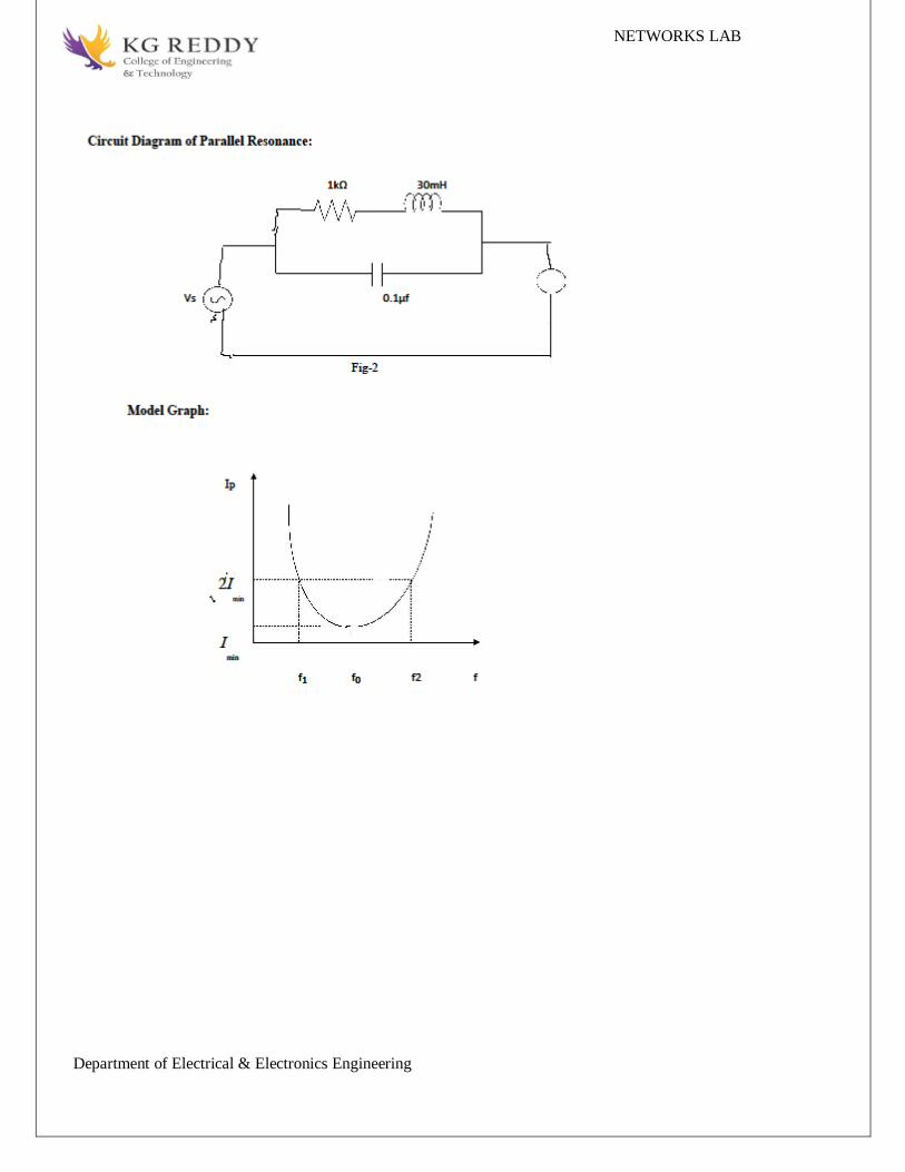
EXPERIMET-4
SERIES AND PARALLE RESONANCE

NETWORKS LAB
Department of Electrical & Electronics Engineering
Circuit Diagram of Series Resonance:

NETWORKS LAB
Department of Electrical & Electronics Engineering
NETWORKS LAB
Department of Electrical & Electronics Engineering

NETWORKS LAB
Department of Electrical & Electronics Engineering
Tabular forms:
Series Resonance
S.no Frequency
(f)
Current
(Is)
Parallel Resonance
S.no Frequency
(f)
Current
(Ip)

NETWORKS LAB
Department of Electrical & Electronics Engineering
Result Table
Series resonance Parallel Resonance
Theoretical Practical Theoretical Practical
Resonant
Frequency(Fo)
Band width(BW)
Quality Factor(Q)
Precautions:
1. Making loose connections are to be avoided
2. Readings should be taken without parallax error
Result:

NETWORKS LAB
Department of Electrical & Electronics Engineering
EXPERIMET-5
TIME RESPONSE OF FIRST ORDER RC / RL NETWORK FORPERIODIC
NON – SINUSOIDAL INPUTS – TIME CONSTANT AND STEADY STATE
ERROR DETERMINATION.
AIM:
To draw the time response of first order series RL and RC network for periodic non-
sinusoidal function and verify the time constant
APPARATUS:
S.no Name of the equipment Range Type Quantity
1 Function generator 1
2 DRB 1
3 DIB 1
4 DCB 1
5 CRO 1
6 CRO Probes As required
7 Connecting wires
Theory:
Theoretical Calculations:
Formula required
For RL Series circuit, time constant T= L/R
For RC Series circuit, Time constant r = RC

NETWORKS LAB
Department of Electrical & Electronics Engineering
Series RL Circuit
Series RC Circuit
Model Graph:
Procedure:
Series RL Circuit:

NETWORKS LAB
Department of Electrical & Electronics Engineering
1. Connections are made as shown in the fig-1.
2. Input voltage (Square wave) is set to a particular value.
3. The waveform of voltage across inductor is observed on CRO and the waveform is drawn on a
Graph sheet.
4. The time constant is found from the graph and verified with the theoretical value.
Series RC Circuit:
1. Connections are made as shown in the fig-2.
2. Input voltage (Square wave) is set to a particular value.
3. The waveform of voltage across the capacitor is observed on CRO and the waveform is drawn
On a graph sheet. 4. The time constant is found from the graph and verified with the theoretical value
Result Table
Series resonance Parallel Resonance
Theoretical Practical Theoretical Practical
Time constant (T)
Precautions:
1. Making loose connections are to be avoided
2. Readings should be taken without parallax error
Result:

NETWORKS LAB
Department of Electrical & Electronics Engineering
EXPERIMENT – 6
TWO PORT NETWORK PARAMETERS – Z – Y PARAMETERS,
ANALYTICAL VERIFICATION.
AIM: To obtain experimentally Z parameters and Y parameters of a given two port network.
APPARATUS:
S.no Name of the equipment Range Type Quantity
1 Trainer kit 1
2 Multi meters MC 2
3 Connecting wires As Required
CIRCUIT DIAGRAM:

NETWORKS LAB
Department of Electrical & Electronics Engineering
Calculation of Z11 and Z21
Calculation of Z12 and Z22
Calculation of Y11 and Y21

NETWORKS LAB
Department of Electrical & Electronics Engineering
Calculation of Y12 and Y22
THEORY:
Open Circuit Impedance Parameters (Z-Parameters):
Z-parameters can be defined by the following equations
V1 = Z11I1 + Z12I2 …………………… (1)
V2 = Z21I1 + Z22I2 …………………… (2)
In Matrix form:

NETWORKS LAB
Department of Electrical & Electronics Engineering
If port 2-21 is open circuited, i.e., I2 = 0, then Z11 = V1/I1 & Z21 = V2/I1
If port 1-11 is open circuited, i.e., I1 = 0, then Z12 = V1/I2 & Z22 = V2/I2
Here,
Z11 is the driving point impedance at port 1-11 with 2-21open circuited. It can also be called as open
circuit input impedance.
Z21 is the transfer impedance at port 1-11 with 2-21 open circuited. It can also be called as open
circuit forward transfer impedance.
Z12 is the transfer impedance at port 2-21 with 1-11 open circuited. It can also be called as open
circuit reverse transfer impedance and
Z22 is the driving point impedance at port 2-21 with 1-11 open circuited. It can also be called as open
circuit output impedance.
Network is
a) Reciprocal then V1/I2 (where I1 = 0) = V2/I1 (where I2 = 0) i.e., Z12 = Z21
b) Symmetrical then V1/I1 (where I2 = 0) = V2/I2 (where I1 = 0) i.e., Z11 = Z22
Short Circuit Admittance Parameters (Y-parameters):
Y-parameters can be defined by the following equations
I1 = Y11V1 + Y12V2 ………………. (1)
I2 = Y21V1 + Y22V2 ………………. (2)
In matrix form
If port 2-21 is short circuited, i.e. V2 = 0 then Y11 = I1/V1 & Y21 = I2/V1
If port 1-11 is short circuited, i.e. V1 = 0 then Y12 = I1/V2 & Y22 = I2/V2
If the network is
a) Reciprocal then I2/V1 (where V2 = 0) = I1/V2 (where V1 = 0) i.e. Y21 = Y12
b) Symmetrical then I1/ V1 (where V2 = 0) = I2/ V2 (where V1 = 0) i.e. Y11 = Y22
PROCEDURE:
1. Open Circuiting Output Terminals (I2 = 0):

NETWORKS LAB
Department of Electrical & Electronics Engineering
Connections are made as per the circuit diagram shown in fig (2). Output terminals are kept
Open via a voltmeter. Supply is given to input port. Note the readings of ammeter as I1 and
Voltmeter as V2.
2. Short circuiting output terminals (V2 = 0):
Connections are made as per the circuit diagram shown in fig (4). Output terminals are short
circuited via an ammeter. Supply is given to input port. Note the readings of ammeters as I1
and I2.
3. Open circuiting input terminals (I1 = 0):
Connections are made as per the circuit diagram shown in fig (3). Input terminals are kept
open via an voltmeter. Supply is given to output terminals. Note the readings of ammeter as I2
and voltmeter as V1.
4. Short circuiting input terminals (V1=0):
Connections are made as per the circuit diagram shown in fig (5). Input terminals are short
circuited via an ammeter. Supply is given to output port. Note the readings of ammeters as I1
and I2.
4. Calculate Z, Y Parameters values.
OBSERVATION TABLES:
When I1=0
When I2=0
When V1=0
When V2=0

NETWORKS LAB
Department of Electrical & Electronics Engineering
RESULT TABLE:
Z-Parameters Y-Parameters
Z11 Z12 Z21 Z22 Y11 Y12 Y21 Y22
Theoretical
Values
Practical
Values
PRECAUTIONS:
1. Avoid making loose connections.
2. Readings should be taken carefully without parallax error.
3. Avoid series connection of voltmeters and parallel connection ammeters.
RESULT:

NETWORKS LAB
Department of Electrical & Electronics Engineering
EXPERIMENT – 7
TWO PORT NETWORK PARAMETERS – A, B, C, D & HYBRID
PARAMETERS, ANALYTICAL VERIFICATION
AIM: To obtain experimentally ABCD parameters and Hybrid parameters of a given two port
network
APPARATUS:
S.no Name of the equipment Range Type Quantity
1 Trainer kit 1
2 Multi meters MC 2
3 Connecting wires As Required
CIRCUIT DIAGRAM:
Calculation Of A And C:

NETWORKS LAB
Department of Electrical & Electronics Engineering
Calculation of B and D
CALCULATION OF H11 And H21

NETWORKS LAB
Department of Electrical & Electronics Engineering
Calculation of h12 and h22
THEORY:
ABCD Parameters:
ABCD parameters can be defined by the following equations
In matrix form

NETWORKS LAB
Department of Electrical & Electronics Engineering
If port 2-21
is open circuited i.e., I2=0 then
A is called reverse voltage ratio and C is known as transfer admittance.
If port 2-21 is short circuited i.e., V2=0 then
B is called transfer impedance and D is called reverse current ratio.
Hybrid Parameters (h-Parameters):
h-parameters can be defined by the following equations
In matrix form:
If port 2-21
is short circuited, i.e. V2 = 0 then
h11 is called input impedance and h21 is called forward current gain.
If port 1-11 is open circuited, i.e., I1=0 then

NETWORKS LAB
Department of Electrical & Electronics Engineering
h22 is called output admittance and h12 is called reverse voltage gain.
PROCEDURE:
1. To find A and C Parameters (I2 = 0):
Connections are made as per the circuit diagram shown in fig (2). Output terminals are kept
Open via voltmeter. Supply is given to input port. Note the readings of ammeter as I1 and
Voltmeters as V1, V2.
2. To find B and D Parameters (V2 = 0):
Connections are made as per the circuit diagram shown in fig (3). Output terminals are short
circuited via an ammeter. Supply is given to input port. Note the readings of ammeters as I1, I2
and voltmeters as V1.
3. To find h11 and h21 (V2 = 0):
Connections are made as per the circuit diagram shown in fig (4). Output terminals are short
circuited via an ammeter. Supply is given to input port. Note the readings of ammeter as I1
and voltmeter as V1.
4. To find h12 and h22 (I1 = 0):
Connections are made as per the circuit diagram shown in fig (5).Input terminals current is
zero. Supply is given to input port. Note the readings of voltmeter as V1 and ammeter as I2.
5. ABCD, Hybrid parameters using formulae and verify them with theoretical values.
OBSERVATION TABLES:
When I2=0
S.No. V1 I1 V2
When V2=0
S.No. V1 I1 I2
When I1=0
S.No. V1 I2 V2
When V1=0
S.No. I2 I1 V2

RESULT TABLE:
PRECAUTIONS:
1. Avoid making loose connections.
2. Readings should be taken carefully without parallax error.
3. Avoid series connection of voltmeters and parallel connection ammeters.
RESULT:

Basic Electrical Simulation Lab
Department of Electrical & Electronics Engineering
EXPERIMENT - 8
SEPARATION OF SELF AND MUTUAL INDUCTANCE IN A COUPLED
CIRCUIT. DETERMINATION OF COEFFICIENT OF COUPLING
Aim:
To determine the self inductance, mutual inductance and coefficient of coupling of single phase
transformer.
Apparatus:
S.No Name of the equipment Range Type Quantity
1 Single phase transformer 1
2 Single phase auto transformer 1
3 Ammeter 1
4 voltmeter 1
5 ammeter 1
6 voltmeter 1
7 Connecting wires As required
Theory:
Self-inductance or in other words inductance of the coil is defined as the property of the
coil due to which it opposes the change of current flowing through it. Inductance is attained by a
coil due to the self-induced emf produced in the coil itself by changing the current flowing
through it.
If we accidentally or purposefully put two inductors close together, we can actually
transfer voltage and current from one inductor to another. This property is called Mutual
Inductance. A device which utilizes mutual inductance to alter the voltage or current output is
called a transformer.
The inductor that creates the magnetic field is called the primary coil, and the inductor that
picks up the magnetic field is called the secondary coil. Transformers are designed to have the
greatest mutual inductance possible by winding both coils on the same core. (In calculations for
inductance, we need to know which materials form the path for magnetic flux. Air core coils have
low inductance; Cores of iron or other magnetic materials are better 'conductors' of magnetic
flux.)

Basic Electrical Simulation Lab
Department of Electrical & Electronics Engineering
The voltage that appears in the secondary is caused by the change in the shared magnetic field,
each time the current through the primary changes. Thus, transformers work on A.C. power, since
the voltage and current change continuously.

Basic Electrical Simulation Lab
Department of Electrical & Electronics Engineering

Basic Electrical Simulation Lab
Department of Electrical & Electronics Engineering

Basic Electrical Simulation Lab
Department of Electrical & Electronics Engineering

Basic Electrical Simulation Lab
Department of Electrical & Electronics Engineering
EXPERIMENT-9
VERIFICATION OF COMPENSATION THEOREM
AIM: To Verify the compensation theorem.
APPARATUS:
S.No. Equipment Range Quantity
1 DC.RPS-Voltage Source 0-30 Volts/2A 1
2 Trainer kit ------------------ 1
3 Ammeter-DC 0-200 mA 1
4 Voltmeter-DC 0-20V or 0-30V 2
5 Connecting wires Single lead As required
THEORY:
Compensation:
“Any impedance in a network of generators and impedance in a network of generators
and impedances can be replaced by a generator of zero internal impedance and of emf equal to the
instantaneous potential difference across the replaced impedance”.
Millmann’s Theorems
” If a number of constant voltage generators, say n, of emf’s V1, V2, V3 ……….
Vn and internal admittances Y1, Y2, Y3………..Yn respectively are connected in parallel, then
resultant potential difference across output terminals AB is given by
VMILLIMAN =
Where Y = 1/Z is the admittance.
PROCEDURE:
1. Set the voltage to 10V and connect voltage sources and ammeters.
Note: Z = 150E should be shorted while taking the mesh analysis.
Applying Mesh Analysis

Basic Electrical Simulation Lab
Department of Electrical & Electronics Engineering
1330I1-330I1 = 10 ……………… (1)
-330I1+480I1 = 0 ………………….(2)
______________________________
I1 = 9.065 mA
I1= 6.23 mA
2. Using compensation theorem find the change in current through 1KE when 150KE is
change to 300E.
Note: Z = 150E should be opened while taking the mesh analysis.
3. Applying mesh analysis
1330i2 – 330i2 = 10 ………………(3)
-330i2 +630i2 = 0……………………(4)
I2 = 8.642 mA
I2 = 4.52 mA
4. Change in current
I1 - I2 = 9.065 – 8.642 = 0.423 m A ……………….(5)
I1 - I2 =6.23 – 4.52 = 1.71m A ………………………(6)
5. Now calculate compensation voltage using equation
Vcomp = -I. …………… (7)
= 6.23×150
= -.9345V
6. Apply the compensation voltage in the compensation equivalent circuit.
Note: Z3 = 300E while taking the mesh analysis
7. Applying mesh analysis
13303i3 – 330i3 = 0…………….(8)
-330i3 + 630i3 = -.9345 ………..(9)
I3 = .4227 m A

Basic Electrical Simulation Lab
Department of Electrical & Electronics Engineering
I3 = 1.704 m A
8. From equations 5 & 7 we observe that the change in current in the linear circuit is equal to
the current observed in compensation equivalent circuit.
PROCEDURE:
1) Connect the voltage sources and ammeter to the terminals provided in circuit diagram.
2) Set the voltage v1 = 10v, v2 = 15v, v3 = 20v.
3) Calculate the Millman’s voltage and Millman’s resistance by the equations given
below
VMILLMAN =
RMILLMAN =
4) Vary ZI and note down the load current in a tabular form.
5) Now apply the Millman’s voltage to the Millman’s equivalent circuit by setting the Zm
to the Millman’s resistance.
6) Vary ZL and note down the current in a tabular form.
7) We observe from the both tables that the load current in the both circuit is same.
Note: In this experiment ZL = 1KE, Z2 = 330E, Z3 = 150E.
We get Millman’s voltage = 17.64v and
Millman’s resistance = 93.45E
MILLIMAN’S THEOREM:
CIRCUIT DIAGRAM:

Basic Electrical Simulation Lab
Department of Electrical & Electronics Engineering
TABULAR COLOUMN:
S.NO. ZL IL (m A )
PRECAUTIONS:
1. Reading must be taken without parallax error.
2. Measuring instruments must be connected properly & should be free from errors.
3. All connections should be free from loose contacts.
4. The direction of currents should be identified correctly.
RESULT:

Basic Electrical Simulation Lab
Department of Electrical & Electronics Engineering
EXPERIMENT – 10
MEASUREMENT OF ACTIVE POWER FOR STAR AND DELTA CONNECTED
BALANCED LOAD
Aim:
Measurement of active and reactive power using 1-wattmeter at different R, L & C loads.
Apparatus:
S.No NAME OF THE
APPARATUS
RANGE QUANTITY
1 UPF Wattmeter’s (0-300V) 1
2 Ammeter (0-10A) 2
3 Voltmeter
(0-300V) 1
4 Balanced Load
Theory:
The active power is obtained by taking the integration of function between a particular time
intervals from t1 to t2.
2
1
)()(
1
12
t
t
dttPtt
P
By integrating the instantaneous power over one cycle, we get average power.
The average power dissipated is
Pav=Veff [Ieff *Cosθ]
From impedance triangle,

Basic Electrical Simulation Lab
Department of Electrical & Electronics Engineering
Cosθ = R/Z
Substituting, we get
Reactive Power Pr = Veff [Ieff *sinθ]
Active power measurement circuit diagram:
Procedure:
a) Connect the circuit as shown in the circuit diagram.
b) Keep all the toggle switches in ON condition.
c) Switch on equal loads on each phase i.e. balanced load must be maintained with
different load combinations.
d) Connect the ammeter in R-Phase and then switch OFF the toggle switch connected
across the ammeter symbol.
e) Connect the pressure coil of the wattmeter across R-Y phase and current coil in R-
phase to measure active power.
Obsevations :
S.No
Vph (Volts) Il (mA) Pph (Var) Pactual
P=3*Pph (Var)
Cosθ = P/( 3VlIl )

Basic Electrical Simulation Lab
Department of Electrical & Electronics Engineering
RESULT:

Basic Electrical Simulation Lab
Department of Electrical & Electronics Engineering
EXPERIMENT – 11
MEASUREMENT OF REACTIVE POWER FOR STAR AND DELTA
CONNECTED BALANCED LOADS
Aim:
Measurement of active and reactive power using 1-wattmeter at different R, L & C loads.
Apparatus:
S.No NAME OF THE
APPARATUS
RANGE QUANTITY
1 UPF Wattmeter’s (0-300V) 1
2 Ammeter (0-10A) 2
3 Voltmeter
(0-300V) 1
4 Balanced Load
THEORY:
Reactive power is the imaginary or complex power in a capacitive or inductive load. Reactive
power represents an energy exchange between the power source and the reactive loads where no
net power is gained or lost. The net average reactive power is zero. Reactive power is stored in
and discharged by inductive motors, transformers, solenoids and capacitors.
Reactive power should be minimized because it increases the overall current flowing in an electric
circuit without providing any work to the load. Increased reactive currents only provide
unrecoverable power loss due to power line resistance.
Increased reactive and apparent powers will devrease the power factor - PF.
Reactive inductive power is measured in volt-amperes reactive (VAR).
Single Phase Current
Q = U I sin φ

Basic Electrical Simulation Lab
Department of Electrical & Electronics Engineering
= U I PF
where
φ = phase angle
Three Phase Current
Q = 31/2 U I sin φ
= 1.732 UI PF
Reactive power measurement circuit diagram:
Procedure:
a) Connect the circuit as shown in the circuit diagram.
b) Keep all the toggle switches in ON condition.
c) Switch on equal loads on each phase i.e. balanced load must be maintained with
different load combinations.
d) Connect the ammeter in R-Phase and then switch OFF the toggle switch connected
across the ammeter symbol.
e) Connect the pressure coil of the wattmeter across R-Y phase and current coil in R-
phase to measure active power.
Tabular forms:
Reactive Power:
Type of the
load
Vph (Volts) Il (mA) Qph (Var) Qactual
Q=3*Qph
(Var)
Cosθ = Q/( 3VlIl )

Basic Electrical Simulation Lab
Department of Electrical & Electronics Engineering
Result: