verdin development board datasheet
TRANSCRIPT

Verdin Development Board
Datasheet

Verdin Development Board Datasheet
Toradex AG l Ebenaustrasse 10 l 6048 Horw l Switzerland l +41 41 500 48 00 l www.toradex.com l [email protected] Page | 2
Revision History
Date Doc. Rev. Board Version
Changes
20-Apr-2021 Rev. 1.00 V1.1 Initial Release.
22-Jun-2021 Rev. 1.01 V1.1 Updated the PHY status LED signal names according to the 1.3 version of the Verdin Family Specification throughout the whole document

Verdin Development Board Datasheet
Toradex AG l Ebenaustrasse 10 l 6048 Horw l Switzerland l +41 41 500 48 00 l www.toradex.com l [email protected] Page | 3
Contents
1 Introduction ........................................................................................................................................ 5 1.1 Reference Documents ......................................................................................................................5
1.1.1 Verdin Family Specification ....................................................................................................5 1.1.2 Verdin Carrier Board Design Guide .......................................................................................5 1.1.3 Verdin Computer on Module family overview ........................................................................5 1.1.4 Toradex Developer Website – Verdin Computer on Module documents ..............................5 1.1.5 Carrier Board Layout Guide ...................................................................................................5 1.1.6 Toradex Developer Website – Verdin Development Board Design Files ..............................5 1.1.7 Pushbutton On/Off controller datasheet ................................................................................5 1.1.8 USB HUB datasheet ..............................................................................................................5 1.1.9 Gigabit Ethernet Transceiver datasheet ................................................................................5 1.1.10 RS232 Transceiver datasheet ...............................................................................................5 1.1.11 RS485 Transceiver datasheet ...............................................................................................6 1.1.12 Audio Codec datasheet ..........................................................................................................6 1.1.13 USB Type-C Configuration Channel Logic IC datasheet .......................................................6 1.1.14 UV/OV and Reverse Protection Controller datasheet............................................................6 1.1.15 GPIO expander datasheet .....................................................................................................6
1.2 Abbreviations ....................................................................................................................................7 1.3 Main Features ...................................................................................................................................9 1.4 Hardware Architecture Block Diagram ........................................................................................... 10 1.5 Physical Drawing ........................................................................................................................... 11
1.5.1 Connectors .......................................................................................................................... 11
2 Interface Description ........................................................................................................................ 14 2.1 Verdin Computer-On-Module ......................................................................................................... 14 2.2 Power Supply ................................................................................................................................. 14
2.2.1 Terminal Block Power Supply Connector (X57) ................................................................. 15 2.2.2 Barrel Jack Power Supply Connector (X58) ....................................................................... 15 2.2.3 Power Out Header (X9, X11) .............................................................................................. 15 2.2.4 Power Control ..................................................................................................................... 15 2.2.5 Power supply input protection ............................................................................................. 17
2.3 Power gating circuit. ....................................................................................................................... 17 2.3.1 GPIO expander header (X8) ............................................................................................... 19 2.3.2 GPIO expander header (X10) ............................................................................................. 19
2.4 Indicator LEDs ............................................................................................................................... 20 2.5 Test Points ..................................................................................................................................... 22 2.6 Ethernet Interface .......................................................................................................................... 24
2.6.1 Ethernet_1 Connector (X25) ............................................................................................... 24 2.6.2 Ethernet_2 Connector (X35) ............................................................................................... 24
2.7 Verdin USB_1 Port ......................................................................................................................... 25 2.7.1 USB_1 Connector (X34) ..................................................................................................... 25
2.8 Verdin USB_2 Port ......................................................................................................................... 26 2.8.1 USB_2 Connector (X53) ..................................................................................................... 27
2.9 PCIe Interface ................................................................................................................................ 27 2.9.1 Mini PCIe Connector (X33) ................................................................................................. 27 2.9.2 SIM Card Holder (X36) ....................................................................................................... 29
2.10 SD Card Interface ....................................................................................................................... 30 2.10.1 SD Card 4bit Connector (X19) ............................................................................................ 30
2.11 Display Interface ......................................................................................................................... 31 2.11.1 HDMI Connector (X11) ....................................................................................................... 31 2.11.2 DSI Display Adapter Connector (X48) ................................................................................ 32
2.12 Audio .......................................................................................................................................... 34 2.12.1 Analog Audio ....................................................................................................................... 34 2.12.2 Digital Audio ........................................................................................................................ 35
2.13 “Module-specific” Interface ......................................................................................................... 36 2.13.1 “Module-specific” Mezzanine Board Connector (X52) ........................................................ 36
2.14 MIPI CSI Camera Interface ........................................................................................................ 40 2.14.1 MIPI CSI Camera Connector (X47) .................................................................................... 40
2.15 Digital and Analog I/O ................................................................................................................ 41

Verdin Development Board Datasheet
Toradex AG l Ebenaustrasse 10 l 6048 Horw l Switzerland l +41 41 500 48 00 l www.toradex.com l [email protected] Page | 4
2.15.1 Communication Interface .................................................................................................... 41 2.16 Digital interfaces ......................................................................................................................... 43
2.16.1 Switches / LEDs .................................................................................................................. 43 2.16.2 Level shifters ....................................................................................................................... 45 2.16.3 Analog Interface .................................................................................................................. 46
2.17 Backup battery ........................................................................................................................... 47 2.17.1 Battery Holder (BAT1) ......................................................................................................... 47
2.18 JTAG .......................................................................................................................................... 47 2.18.1 JTAG Connector (X56) ....................................................................................................... 47
2.19 USB Debugger ........................................................................................................................... 48 2.20 Low-speed IO pins configuration ................................................................................................ 50
2.20.1 Low-speed IO pins 1 Male (X3 Row A and B) .................................................................... 51 2.20.2 Low-speed IO pins 1 Female (X2) ...................................................................................... 52 2.20.3 Function 1 Female (X4) ...................................................................................................... 52 2.20.4 Low-speed IO pins 2 Male (X6 Row A and B) .................................................................... 53 2.20.5 Function 2 Female (X5) ...................................................................................................... 54 2.20.6 Low-speed IO pins 2 Female (X7) ...................................................................................... 54 2.20.7 Low-speed IO pins 3 Male (X16 Row A and B) .................................................................. 55 2.20.8 Low-speed IO pins 3 Female (X15) .................................................................................... 56 2.20.9 Function 3 Female (X17) .................................................................................................... 56
3 Mechanical Data ............................................................................................................................... 57
4 Design Data ....................................................................................................................................... 58
5 Product Compliance ........................................................................................................................ 58

Verdin Development Board Datasheet
Toradex AG l Ebenaustrasse 10 l 6048 Horw l Switzerland l +41 41 500 48 00 l www.toradex.com l [email protected] Page | 5
1 Introduction
The Verdin Development Board is a flexible development board with which you can explore and
evaluate the functionality and performance of the Verdin product family.
Complementing the Verdin computer on module, Verdin Development Board supports a wide variety
of industry-standard interfaces while at the same time providing advanced multimedia and high-
speed connectivity options, making it suitable for an almost unlimited number of applications. Verdin
interfaces can be easily accessed using physical connectors and standard pitch headers.
The Verdin Development Board is built on a 4-layer printed circuit board (PCB), and only one layer is
used for high-speed signal routing. This demonstrates how Direct Breakout technology makes it
incredibly easy to implement leading-edge interfaces with minimal risk and effort. CAE data for the
board, including schematics, layout, and IPC-7351 compliant component libraries, are freely
downloadable from the Toradex developer website.
1.1 Reference Documents
For detailed technical information, please refer to the documents listed below.
1.1.1 Verdin Family Specification
https://docs.toradex.com/109262-verdin-family-specification.pdf
1.1.2 Verdin Carrier Board Design Guide
https://docs.toradex.com/108140-verdin-carrier-board-design-guide.pdf
1.1.3 Verdin Computer on Module family overview
https://www.toradex.com/computer-on-modules/Verdin-arm-family
1.1.4 Toradex Developer Website – Verdin Computer on Module documents
https://developer.toradex.com/products/verdin-som-family/modules
1.1.5 Carrier Board Layout Guide
https://docs.toradex.com/102492-layout-design-guide.pdf
1.1.6 Toradex Developer Website – Verdin Development Board Design Files
https://developer.toradex.com/products/verdin-development-board
1.1.7 Pushbutton On/Off controller datasheet
https://www.analog.com/media/en/technical-documentation/data-sheets/2954fb.pdf
1.1.8 USB HUB datasheet
https://ww1.microchip.com/downloads/en/DeviceDoc/USB5744-Data-Sheet-DS00001855J.pdf
1.1.9 Gigabit Ethernet Transceiver datasheet
https://ww1.microchip.com/downloads/en/DeviceDoc/00002841B.pdf
1.1.10 RS232 Transceiver datasheet
https://www.ti.com/lit/ds/symlink/trs3122e.pdf
Verdin Development Board Datasheet
Toradex AG l Ebenaustrasse 10 l 6048 Horw l Switzerland l +41 41 500 48 00 l www.toradex.com l [email protected] Page | 6
1.1.11 RS485 Transceiver datasheet
https://www.ti.com/lit/ds/symlink/sn65hvd01.pdf
1.1.12 Audio Codec datasheet
https://www.nuvoton.com/export/resource-files/DS_NAU88C22_DataSheet_EN_Rev1.1.pdf
1.1.13 USB Type-C Configuration Channel Logic IC datasheet
https://www.ti.com/lit/ds/symlink/tusb321ai.pdf
1.1.14 UV/OV and Reverse Protection Controller datasheet
https://www.analog.com/media/en/technical-documentation/data-sheets/LTC4368.pdf
1.1.15 GPIO expander datasheet
https://www.nxp.com/docs/en/data-sheet/PCAL6416A.pdf

Verdin Development Board Datasheet
Toradex AG l Ebenaustrasse 10 l 6048 Horw l Switzerland l +41 41 500 48 00 l www.toradex.com l [email protected] Page | 7
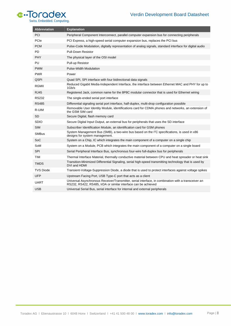
1.2 Abbreviations
Abbreviation Explanation
ADC Analog to Digital Converter
CAN Controller Area Network, a bus that is mainly used in the automotive and industrial environment
CAN FD Controller Area Network Flexible Data-Rate, an extension to the original CAN bus protocol which allows higher data rates and larger message sizes.
CEC Consumer Electronic Control, HDMI feature that allows controlling CEC compatible devices
CPU Central Processor Unit
CSI Camera Serial Interface
DAC Digital to Analog Converter
DDC Display Data Channel, interface for reading out the capability of a monitor. In this document DDC2B (based on I2C) is always meant
DFP Downstream Facing Port, USB Type-C port that acts as a host
DRP Dual-Role Port, USB Type-C port that can operate as power sink and source
DSI Display Serial Interface
DVI Digital Visual Interface, digital signals are electrically compatible with HDMI
EDID Extended Display Identification Data, timing setting information provided by the display in a PROM
EMI Electromagnetic Interference, high-frequency disturbances
ESD Electrostatic Discharge, high voltage spike or spark that can damage electrostatic- sensitive devices
FPD-Link Flat Panel Display Link, high-speed serial interface for liquid crystal displays. In this document is also called the LVDS interface.
GBE Gigabit Ethernet, Ethernet interface with a maximum data rate of 1000Mbit/s
GND Ground
GND_CHASSIS Chassis Ground
GPIO General Purpose Input/Output, pin that can be configured as an input or output
GSM Global System for Mobile Communications
HDA High-Definition Audio (HD Audio), the digital audio interface between CPU and audio codec
I2C Inter-Integrated Circuit, the two-wire interface for connecting low-speed peripherals
I2S Integrated Interchip Sound, serial bus for connecting PCM audio data between two devices
I/O Input-Output
JTAG Joint Test Action Group, widely used debug interface
LCD Liquid Crystal Display
LSB Least Significant Bit
LVDS
Low-Voltage Differential Signaling, electrical interface standard that can transport high-speed signals over twisted-pair cables. Many interfaces like PCIe or SATA use this interface. Since the first successful application was the Flat Panel Display Link, LVDS became a synonymous for this interface. In this document, the term LVDS is used for the FPD-Link interface.
MAC Medium Access Control is part of the second layer (data link layer) in the Ethernet stack
MIPI Mobile Industry Processor Interface Alliance
MDI Medium Dependent Interface, the physical interface between Ethernet PHY and cable connector
MDIO Management Data Input/Output, an interface that is used for controlling the Ethernet PHY. The bus consists of the MDC clock and the MDIO bidirectional data signal.
mini PCIe PCI Express Mini Card, the card form factor for internal peripherals. The interface features PCIe and USB 2.0 connectivity
MMC MultiMediaCard, flash memory card
MSB Most Significant Bit
NC Not Connected
OD Open-Drain
OTG USB On-The-Go, a USB host interface that can also act as USB client when connected to another host interface
PCB Printed Circuit Board
Verdin Development Board Datasheet
Toradex AG l Ebenaustrasse 10 l 6048 Horw l Switzerland l +41 41 500 48 00 l www.toradex.com l [email protected] Page | 8
Abbreviation Explanation
PCI Peripheral Component Interconnect, parallel computer expansion bus for connecting peripherals
PCIe PCI Express, a high-speed serial computer expansion bus, replaces the PCI bus
PCM Pulse-Code Modulation, digitally representation of analog signals, standard interface for digital audio
PD Pull-Down Resistor
PHY The physical layer of the OSI model
PU Pull-up Resistor
PWM Pulse-Width Modulation
PWR Power
QSPI Quad SPI, SPI interface with four bidirectional data signals
RGMII Reduced Gigabit Media-Independent Interface, the interface between Ethernet MAC and PHY for up to 1Gb/s
RJ45 Registered Jack, common name for the 8P8C modular connector that is used for Ethernet wiring
RS232 The single-ended serial port interface
RS485 Differential signaling serial port interface, half-duplex, multi-drop configuration possible
R-UIM Removable User Identity Module, identifications card for CDMA phones and networks, an extension of the GSM SIM card
SD Secure Digital, flash memory card
SDIO Secure Digital Input Output, an external bus for peripherals that uses the SD interface
SIM Subscriber Identification Module, an identification card for GSM phones
SMBus System Management Bus (SMB), a two-wire bus based on the I2C specifications, is used in x86 designs for system management.
SoC System on a Chip, IC which integrates the main component of a computer on a single chip
SoM System on a Module, PCB which integrates the main component of a computer on a single board
SPI Serial Peripheral Interface Bus, synchronous four-wire full-duplex bus for peripherals
TIM Thermal Interface Material, thermally conductive material between CPU and heat spreader or heat sink
TMDS Transition-Minimized Differential Signaling, serial high-speed transmitting technology that is used by DVI and HDMI
TVS Diode Transient-Voltage-Suppression Diode, a diode that is used to protect interfaces against voltage spikes
UFP Upstream Facing Port, USB Type-C port that acts as a client
UART Universal Asynchronous Receiver/Transmitter, serial interface, in combination with a transceiver an RS232, RS422, RS485, IrDA or similar interface can be achieved
USB Universal Serial Bus, serial interface for internal and external peripherals
Verdin Development Board Datasheet
Toradex AG l Ebenaustrasse 10 l 6048 Horw l Switzerland l +41 41 500 48 00 l www.toradex.com l [email protected] Page | 9
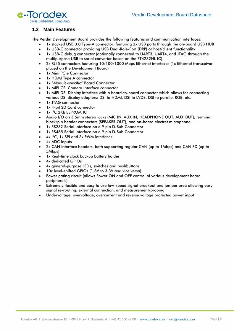
1.3 Main Features
The Verdin Development Board provides the following features and communication interfaces:
• 1x stacked USB 3.0 Type-A connector, featuring 2x USB ports through the on-board USB HUB
• 1x USB-C connector providing USB Dual-Role-Port (DRP) or host/client functionality
• 1x USB-C debug connector (optionally connected to UART3, UART4, and JTAG through the
multipurpose USB to serial converter based on the FT4232HL IC)
• 2x RJ45 connectors featuring 10/100/1000 Mbps Ethernet interfaces (1x Ethernet transceiver
placed on the Development Board)
• 1x Mini PCIe Connector
• 1x HDMI Type A connector
• 1x “Module-specific” Board Connector
• 1x MIPI CSI Camera Interface connector
• 1x MIPI DSI Display interface with a board-to-board connector which allows for connecting
various DSI display adapters: DSI to HDMI, DSI to LVDS, DSI to parallel RGB, etc.
• 1x JTAG connector
• 1x 4-bit SD Card connector
• 1x I2C 2Kb EEPROM IC
• Audio I/O on 3.5mm stereo jacks (MIC IN, AUX IN, HEADPHONE OUT, AUX OUT), terminal
block/pin header connectors (SPEAKER OUT), and on-board electret microphone
• 1x RS232 Serial Interface on a 9-pin D-Sub Connector
• 1x RS485 Serial Interface on a 9-pin D-Sub Connector
• 4x I2C, 1x SPI and 3x PWM interfaces
• 4x ADC inputs
• 2x CAN interface headers, both supporting regular CAN (up to 1Mbps) and CAN FD (up to
5Mbps)
• 1x Real-time clock backup battery holder
• 4x dedicated GPIOs
• 4x general-purpose LEDs, switches and pushbuttons
• 10x level-shifted GPIOs (1.8V to 3.3V and vice versa)
• Power gating circuit (allows Power ON and OFF control of various development board
peripherals)
• Extremely flexible and easy to use low-speed signal breakout and jumper area allowing easy
signal re-routing, external connection, and measurement/probing
• Undervoltage, overvoltage, overcurrent and reverse voltage protected power input

Verdin Development Board Datasheet
Toradex AG l Ebenaustrasse 10 l 6048 Horw l Switzerland l +41 41 500 48 00 l www.toradex.com l [email protected] Page | 10
1.4 Hardware Architecture Block Diagram
US B-C
Connector
US B-C DRP
Controller
T USB321
US B Power
Switc h
AO Z1353DI-01
2x5 Pin
JTAG
Connector
JUM PERSUS B-C
Connector
US B to Seria l
Conv erter
FT4232HL
Termi na l
Block
Connector
Barre l Ja ck
Connector
RECO VERY
Button
RESET
Button
O N/O FF
Button
Button a nd
Power Control
Section
Input protection
Controller
LTC4368I DD-2
Power
Supply
JUM PERS
JUM PERS
JUM PERS
JUM PERS
JUM PERS
Power g ating
circ ui t
PCAL6416AHF
Current sensor
IN A219BID R
1x10 Pi n
Fema le
Hea der
1x10 Pi n
Fema le
Hea der
JUM PERS
M odul-specif ic
M ezza nine
Connector
2x3 Pin
Fema le
Hea der
2x5 Pin
M ale
Hea der
Isola ted
DC-DC
NTE0505M C-R
Isola ted
CAN Tra nsc ei ver
IS O1042BDWR
CR2032
Battery
Holder
JUM PERS
JUM PERS
Tem perature
Sensor
TMP75C
JUM PERS
US B-A
3.x
Connector
US B Power
Switc h
AO Z1353DI-01
US B HU B
US B5744
US B Power
Switc h
AO Z1353DI-01
JUM PERS
M ini PCIe
Connector
Na no SI M Ca rd
Connector
JUM PERS
JUM PERS
T ora dex
CSI Cam era
Connector
SD Card
Connector
RJ45
Connector
RJ45
Connector
Ethernet PHY
KSZ 9131RN XI
D-Sub9
Connector
RS485
Tra nsceiver
SN 65H VD01D RCRJUM PERS
D-Sub9
Connector
RS232
Tra nsceiver
T RS 3122EJUM PERS
HD MI
Type A
Connector
ESD Protec ti on &
conditioning
HD MI 2C1-14H DJUM PERS
EEPROM
M 24C02 F MN 6TP
JUM PERS
JUM PERS
Audio
Codec
NA U88C22YG
JUM PERS
Verdi n DSI
Di spl ay Adapter
Connector
O n-board
M icrophone
CMEJ-0706-42-P
Speak er
Connector
3.5mm
Audio Jack
Connector
3.5mm
Audio Jack
Connector
3.5mm
Audio Jack
Connector
3.5mm
Audio Jack
Connector
LI NE OU T (S TEREO )
LI NE IN (S TEREO)
HP O UT (STEREO)
M IC IN (STEREO)
M IC OU T
SPEAKER O UT (STEREO/BTL)
M IPI DS I
I2S
PWM
2x G PI O
I2C (DDC)
I2S
PWM
2x G PI O
I2C (DDC)
I2C
I2C
I2S I2S
HPD
CEC
I2C (DDC)
HPD
CEC
I2C (DDC)
HD MI HD MI
HPD
CEC
UA RT UA RT RS232
UA RT UA RT RS485
RGM II
M DIO
M DI
LED1
LED2
M DI
LE D1
LED2
SD IO
CDCD
PWR ENPWR EN
I2C
4x G PI O
CAM_M CK
I2C
4x G PI O
CAM_M CK
I2C
4x G PI O
M IPI CS I
UI M
PCIe
PCIe RES ET
WAKE WAKE
SM Bus
US
B (
2.0)
VBUS EN/O C
US B (2. 0)
US B (3. x)
VBUS EN/O C
US B (2. 0)
US B (3. x)
EN EN
O C
VCC BACKUP VCC BACKUP
CAN CAN CAN
2x5 Pin
M ale
Hea der
Isola ted
DC-DC
NTE0505M C-R
Isola ted
CAN Tra nsc ei ver
IS O1042BDWRJUM PERS
CAN CAN CAN
4x AD C
M SP
SPI
Q SPI
2x PWM
4x G PI O
SL EE P
+1. 8V
SoM
PW
R
General-purpose level shifters
4x G PI O
4x G PI O
2x G PI O 2x G PI O
4x G PI O
4x G PI O
PWR CTRL BU S To peri pherals
O C
EN
US B ID
JTAGJTAG
2x U ART
PW R BTN
RESET
RE CO VE RY
FO RCE OF F
BOA RD PWR EN
2x U ART
PWR BTN
RESET
RE CO VE RY
FO RCE OF F
BOA RD PWR EN
PWR CTRL
SoM PWR
BOA RD PWR
FOR
CE
OF
F
PW
R EN
BO
ARD
PW
R E
N
PWR INPWR IN
RECO VERY BTN
RESET BTN
O N/O FF BTN
2x U ART
JTAG
4x G PI O
US B (2. 0)
US B (2. 0)
VBUS
VBUS
CC1
CC2
O C
E N
US B ID
US B (2. 0)
US B (3. x)
Ve
rdin
Ed
ge C
on
ne
cto
r(D
D4
SO
-DIM
M)
2x3 Pin
Fema le
Hea der
I2C
Figure 1: Verdin Development Board Hardware Architecture

Verdin Development Board Datasheet
Toradex AG l Ebenaustrasse 10 l 6048 Horw l Switzerland l +41 41 500 48 00 l www.toradex.com l [email protected] Page | 11
1.5 Physical Drawing
1.5.1 Connectors
Figure 2: Verdin Development Board connectors and controls

Verdin Development Board Datasheet
Toradex AG l Ebenaustrasse 10 l 6048 Horw l Switzerland l +41 41 500 48 00 l www.toradex.com l [email protected] Page | 12
Ref Description Remarks
X1 Verdin module edge connector (DDR4 SO-DIMM)
X2 Verdin edge connector breakout section 1
X3 Verdin edge connector breakout section 1
X4 Verdin edge connector breakout section 1
X5 Verdin edge connector breakout section 2
X6 Verdin edge connector breakout section 2
X7 Verdin edge connector breakout section 2
X8 I2C GPIO Expander I/Os header
X9 Power out header
X10 I2C GPIO Expander I/Os header
X11 Power out header
X13 Analog audio SPEAKER OUT 3-pin header Stereo
X14 Analog audio AUX OUT jack Auxiliary out / Line out (Stereo)
X15 Verdin edge connector breakout section 3
X16 Verdin edge connector breakout section 3
X17 Verdin edge connector breakout section 3
X18 POGO pins
X19 POGO pins
X20 Analog audio HEADPHONE OUT jack Stereo
X21 Analog audio AUX IN jack Auxiliary in / Line in (Stereo)Stereo
X22 Analog audio MIC IN jack Stereo
X23 User button and switch header
X24 User button and switch header
X25 Ethernet connector Ethernet_1
X26 User button and switch header
X27 User button and switch header
X28 Analog audio SPEAKER OUT connector Mono (screwless connector)
X29 Analog audio SPEAKER OUT 2-pin header Mono
X33 Mini PCIe connector
X34 USB DRP connector USB-C (USB 2.0 only)
X35 Ethernet connector Ethernet_2
X36 SIM Card Holder Nano SIM
X37 HDMI connector
X38 User LEDs header
X39 Level shifter header 3.3V
X40 Level shifter header 1.8V
X47 MIPI CSI Camera connector
X48 MIPI DSI Display Adapter connector
X49 ADC input header
X50 RS485 connector 9-pin D-Sub
X51 RS232 connector 9-pin D-Sub
X52 “Module-specific” mezzanine board connector
X53 2x USB3.x HOST connector UPPER: USBH3 – LOWER: USBH2
Verdin Development Board Datasheet
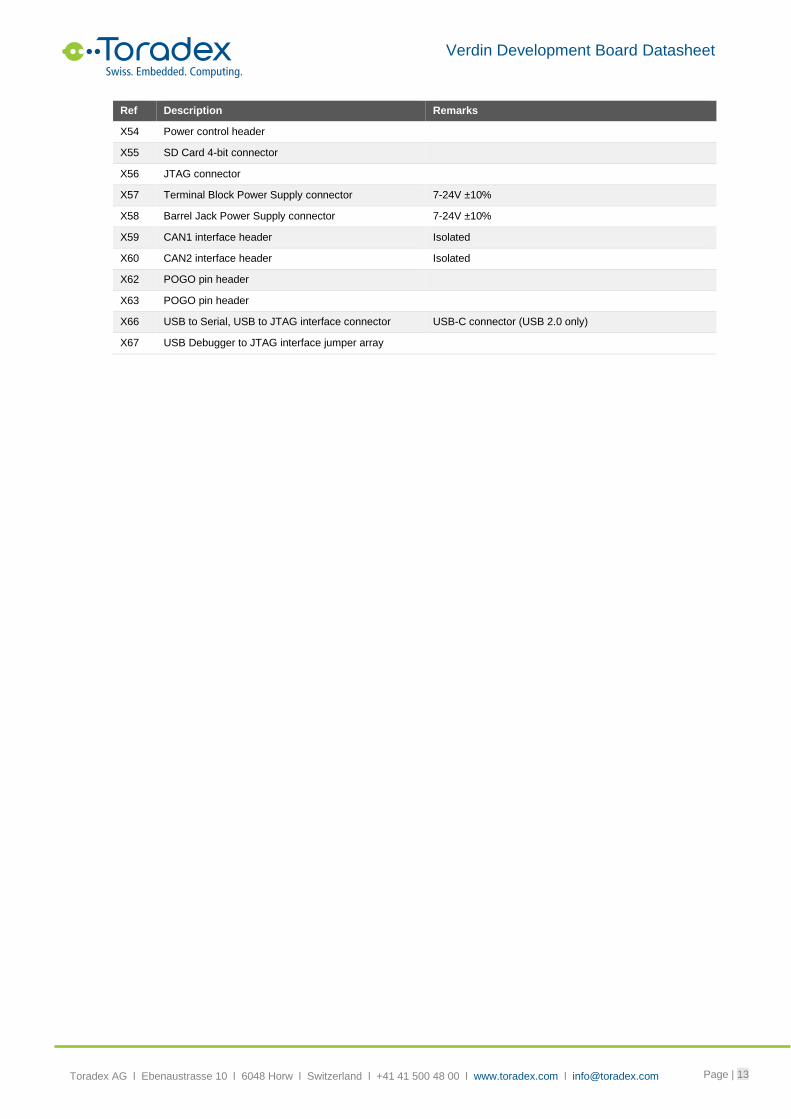
Toradex AG l Ebenaustrasse 10 l 6048 Horw l Switzerland l +41 41 500 48 00 l www.toradex.com l [email protected] Page | 13
Ref Description Remarks
X54 Power control header
X55 SD Card 4-bit connector
X56 JTAG connector
X57 Terminal Block Power Supply connector 7-24V ±10%
X58 Barrel Jack Power Supply connector 7-24V ±10%
X59 CAN1 interface header Isolated
X60 CAN2 interface header Isolated
X62 POGO pin header
X63 POGO pin header
X66 USB to Serial, USB to JTAG interface connector USB-C connector (USB 2.0 only)
X67 USB Debugger to JTAG interface jumper array
Verdin Development Board Datasheet
Toradex AG l Ebenaustrasse 10 l 6048 Horw l Switzerland l +41 41 500 48 00 l www.toradex.com l [email protected] Page | 14
2 Interface Description
2.1 Verdin Computer-On-Module
Type: 260 pin DDR4 SODIMM socket. Manufacturer: TE 2309409-2
For the pinout of the Verdin module, please refer to the applicable Verdin module datasheet or to
the Verdin Family Specification / Verdin Carrier Board Design guide for the abstract pinout.
Stand-offs are available on Verdin Development Board for affixing the Verdin module to the
Development Board. It is recommended to use M2x0.4 size screws to fasten the Verdin module
with the stand-offs.
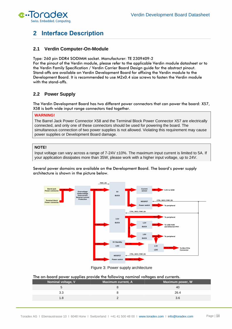
2.2 Power Supply
The Verdin Development Board has two different power connectors that can power the board: X57,
X58 is both wide input range connectors tied together.
Several power domains are available on the Development Board. The board’s power supply
architecture is shown in the picture below.
Figure 3: Power supply architecture
The on-board power supplies provide the following nominal voltages and currents.
Nominal voltage, V Maximum current, A Maximum power, W
5 8 40
3.3 8 26.4
1.8 2 3.6
WARNING!
The Barrel Jack Power Connector X58 and the Terminal Block Power Connector X57 are electrically connected, and only one of these connectors should be used for powering the board. The simultaneous connection of two power supplies is not allowed. Violating this requirement may cause power supplies or Development Board damage.
NOTE!
Input voltage can vary across a range of 7-24V ±10%. The maximum input current is limited to 5A. If your application dissipates more than 35W, please work with a higher input voltage, up to 24V.
Barrel jackPower connector
Currentsensor
5V
BUCK
3.3V
BUCK
1.8V
BUCK
1.2V
BUCK
+V1.2_SW
+V1.8_SW
PMIC_EN
MOSFET
Power switch To peripheral
1.5V
LDO
+V1.5_PCIE_1
Terminal blockPower connector
MOSFET
Power switch
CTRL_MOCI_PWR_EN
5.0V to SOMOvervoltage
UndervoltageOvercurrent
Reverse currentProtection
+V_SUPPLY_FILT_SW
+V5_SW+V5
+V3.3_SW
+V_SUPPLY_FILT
+V_SUPPLY_FILT
5V Standby
LDO
+V5_STB
+V_SUPPLY_FILT
+V_SUPPLY_FILT+V_PWR_IN_1 VCC
+V
3.3
_S
W
+V5
To peripheral
To USB HUBand Ethernet PHY
To peripheral
To Mini PCIe Connector
CTRL_MOCI_PWR_EN
CTRL_MOCI_PWR_EN

Verdin Development Board Datasheet
Toradex AG l Ebenaustrasse 10 l 6048 Horw l Switzerland l +41 41 500 48 00 l www.toradex.com l [email protected] Page | 15
2.2.1 Terminal Block Power Supply Connector (X57)
Connector type: AUK TB5102PRB-H
Pin Description Voltage / Range
1 GND
2 +V_PWR_IN_1 7-24V ±10%
2.2.2 Barrel Jack Power Supply Connector (X58)
Connector type: SWC RAPC722X
Pin Description Voltage / Range
1 +V_PWR_IN_1 7-24V ±10%
2 GND
2.2.3 Power Out Header (X9, X11)
Two female pin headers X9, X11, with main system voltages are available on it, can be used for
powering external boards and modules. Pinout of the X9, X11 connectors is identical.
Connector type: 1x6 Pin Header Female, 2.54mm pitch
Pin Description Remarks
1 +V_SUPPLY_FILT_SW
2 +V5_SW
3 GND
4 +V3.3_SW
5 +V3.3_SW
6 +V1.8_SW
2.2.4 Power Control
The Verdin Development Board power control is implemented using the Linear LTC2954
Pushbutton On/Off controller and with the signal CTRL_PWR_EN_MOCI, used to enable the
peripheral power supplies.
For further information about the signals provided by the LTC2954 controller, please refer to its
datasheet. For more information regarding the power-up sequence implemented on the board,
please refer to the document “Verdin Carrier Board Design Guide”.
The switches SW1 and SW2 have been assigned to the RESET and ON/OFF functions, respectively.
The SW3 is used to put the installed Verdin Computer Module into RECOVERY mode.
Board power also can be controlled by the Verdin Computer Module with an open drain (OD)
CTRL_FORCE_OFF_MOCI# signal. This feature allows the Verdin module to perform a proper
power-down procedure. For more details, please refer to the “Verdin Carrier Board Design Guide”.
The Power CTRL connector X54 allows the Reset and Power Button control signals to be accessed
externally.

Verdin Development Board Datasheet
Toradex AG l Ebenaustrasse 10 l 6048 Horw l Switzerland l +41 41 500 48 00 l www.toradex.com l [email protected] Page | 16
2.2.4.1 Power Control Header (X54)
Connector type: 2x3 Pin Header Female, 2.54mm pitch
Pin Signal Name IO Type Voltage Pull-up/Pull-down Description
1 PWR_BTN# I/O (OD) +1.9V 100k to +1.9V
It is connected to the POWER ON/OFF button SW2. Pulled-up to 1.9V inside pushbutton controller IC. Short pulling down turning on Development Board power and Computer Module. Long pulling down forcing Development Board power off.
2 GND PWR
3 PWR_CTRL I +3.3V max 100k to GND
Behaviour is similar to the “Always ON” Jumper JP7. HIGH level on the PWR_CTRL input forcing on the Verdin Development Board power.
4 CTRL_PWR_BTN_MICO# I/O (OD) +1.8V on SoM
Pulling down for a longer period of time is shutting down the module. Short pulling down is turning on module from off state. Open-drain input with 100k pull-up resistor to the 1.8V RTC rail is on the module. The signal can be left floating on carrier boards
5 CTRL_FORCE_OFF_MOCI# I/O (OD) +5V 100k to +V5_STB
Forcing the turning-off of the main power rail. This signal is ignored for the first 512ms during the power-up sequence. The signal is 5V tolerant.
6 CTRL_RESET_MICO# I/O (OD) +1.8V on SoM
Open-drain input, which resets the module if shorted to ground. There is an on-module pull-up. This means it can be left floating on the carrier board.
Pin 3 of the X54 connector can be used to override the Pushbutton controller. The following table
shows the behavior of the board according to the level of the PWR_CTRL signal:
PWR_CTRL Description
0V The Pushbutton controller is working normally
3.3V The Verdin Development Board is Always On when power is applied
2.2.4.2 Always-ON Jumper (JP7)
Jumper JP7 can be used to configure the “Always On” behaviour.
Type: 1x2 Pin Header Male, 2.54 mm pitch
Jumper position Description
OPEN The board power supply is controlled with Power On/Off buttons.
CLOSED The board power supply will be in the “Always On” state. Verdin Development Board will be powered up as soon as external power is applied to the connector X57 or X58.
By default, jumper JP7 is open.

Verdin Development Board Datasheet
Toradex AG l Ebenaustrasse 10 l 6048 Horw l Switzerland l +41 41 500 48 00 l www.toradex.com l [email protected] Page | 17
2.2.5 Power supply input protection
Supply input is protected against ESD strikes, reverse voltage polarity, overvoltage, undervoltage,
and short circuits. The protection circuit is based on an LTC4368 IC from Analog Devices. For
detailed information, please refer to the LTC4368 datasheet
https://www.analog.com/media/en/technical-documentation/data-sheets/LTC4368.pdf.
Power supply input ratings
Parameter name Min Typ Max Unit
Input voltage (Absolute maximum, limited with an ESD diode) ±30 V
Undervoltage threshold 4.82 4.99 5.17 V
Overvoltage threshold 26.11 27.08 28.09 V
Overcurrent protection 3.96 5 6.06 A
Reverse current protection 99 300 505 mA
Recommended input voltage 6.3 7-24 26.4 V
Jumper JP23 can be used to turn ON or OFF the retry function of the power supply input protection
circuit.
Type: 1x3 Pin Header Male, 2.54 mm pitch
Jumper position Description
1-2 Power supply input will restart automatically after a forward overcurrent fault. The restart delay time is defined by capacitor C300 (5.5ms/nF). The typical value for the Verdin Development Board is 550ms
2-3 Power supply input stays OFF after a forward overcurrent fault. The external power supply should be switched OFF and ON to restore the board power.
By default, jumper JP23 is in position 1-2.
A current, voltage and power measurement IC INA219 (IC27) is also available on Verdin
Development Boards. This IC provides an option to measure the power consumption of Verdin
modules. IC27 is accessible on the I2C_1 bus at address 0x40.
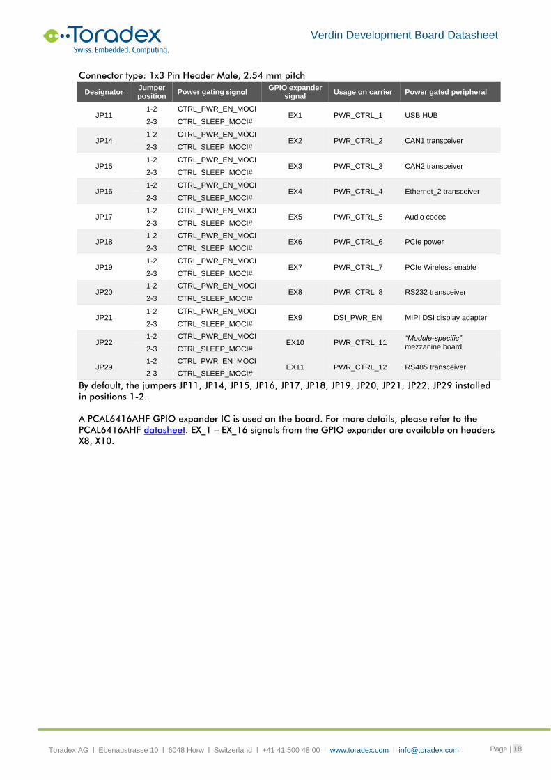
2.3 Power gating circuit.
The Verdin development board contains a power gating circuit. This circuit allows for switching ON
and OFF separate peripheral modules and provides LEDs to show the respective peripheral
module's power state.
There are 3 sources of power gating signals: CTRL_PWR_EN_MOCI, CTRL_SLEEP_MOCI#, EX_1 –
EX_11 (from I2C GPIO expander). Please note that when EX_1 – EX_11 signals are High, then the
respective peripheral is powered up. PWR_CTRL_1 – PWR_CTRL_11 signals which are going directly
to peripherals are not inverted! The source of the power gating signal for each peripheral can be
selected via jumpers.
Figure 4: Part of the power gating schematic
The jumpers JP11, JP14, JP15, JP16, JP17, JP18, JP19, JP20, JP21, JP22, JP29 serve the purpose of
selecting the power gating source signals.
Verdin Development Board Datasheet
Toradex AG l Ebenaustrasse 10 l 6048 Horw l Switzerland l +41 41 500 48 00 l www.toradex.com l [email protected] Page | 18
Connector type: 1x3 Pin Header Male, 2.54 mm pitch
Designator Jumper position
Power gating signal GPIO expander
signal Usage on carrier Power gated peripheral
JP11 1-2 CTRL_PWR_EN_MOCI
EX1 PWR_CTRL_1 USB HUB 2-3 CTRL_SLEEP_MOCI#
JP14 1-2 CTRL_PWR_EN_MOCI
EX2 PWR_CTRL_2 CAN1 transceiver 2-3 CTRL_SLEEP_MOCI#
JP15 1-2 CTRL_PWR_EN_MOCI
EX3 PWR_CTRL_3 CAN2 transceiver 2-3 CTRL_SLEEP_MOCI#
JP16 1-2 CTRL_PWR_EN_MOCI
EX4 PWR_CTRL_4 Ethernet_2 transceiver 2-3 CTRL_SLEEP_MOCI#
JP17 1-2 CTRL_PWR_EN_MOCI
EX5 PWR_CTRL_5 Audio codec 2-3 CTRL_SLEEP_MOCI#
JP18 1-2 CTRL_PWR_EN_MOCI
EX6 PWR_CTRL_6 PCIe power 2-3 CTRL_SLEEP_MOCI#
JP19 1-2 CTRL_PWR_EN_MOCI
EX7 PWR_CTRL_7 PCIe Wireless enable 2-3 CTRL_SLEEP_MOCI#
JP20 1-2 CTRL_PWR_EN_MOCI
EX8 PWR_CTRL_8 RS232 transceiver 2-3 CTRL_SLEEP_MOCI#
JP21 1-2 CTRL_PWR_EN_MOCI
EX9 DSI_PWR_EN MIPI DSI display adapter 2-3 CTRL_SLEEP_MOCI#
JP22 1-2 CTRL_PWR_EN_MOCI
EX10 PWR_CTRL_11 “Module-specific” mezzanine board 2-3 CTRL_SLEEP_MOCI#
JP29 1-2 CTRL_PWR_EN_MOCI
EX11 PWR_CTRL_12 RS485 transceiver 2-3 CTRL_SLEEP_MOCI#
By default, the jumpers JP11, JP14, JP15, JP16, JP17, JP18, JP19, JP20, JP21, JP22, JP29 installed
in positions 1-2.
A PCAL6416AHF GPIO expander IC is used on the board. For more details, please refer to the
PCAL6416AHF datasheet. EX_1 – EX_16 signals from the GPIO expander are available on headers
X8, X10.

Verdin Development Board Datasheet
Toradex AG l Ebenaustrasse 10 l 6048 Horw l Switzerland l +41 41 500 48 00 l www.toradex.com l [email protected] Page | 19
2.3.1 GPIO expander header (X8)
Connector type: 1x10 Pin Header Female, 2.54 mm pitch
Pin Signal Name I/O Type Voltage Pull-up/Pull-down
1 GND PWR
2 EX_1 O +1.8V 10k to +V1.8_SW
3 EX_2 O +1.8V 10k to +V1.8_SW
4 EX_3 O +1.8V 10k to +V1.8_SW
5 EX_4 O +1.8V 10k to +V1.8_SW
6 EX_5 O +1.8V 10k to +V1.8_SW
7 EX_6 O +1.8V 10k to +V1.8_SW
8 EX_7 O +1.8V 10k to +V1.8_SW
9 EX_8 O +1.8V 10k to +V1.8_SW
10 +V1.8_SW PWR +1.8V
2.3.2 GPIO expander header (X10)
Connector type: 1x10 Pin Header Female, 2.54 mm pitch
Pin Signal Name I/O Type Voltage Pull-up/Pull-down
1 GND PWR
2 EX_9 O +1.8V 10k to +V1.8_SW
3 EX_10 O +1.8V 10k to +V1.8_SW
4 EX_11 O +1.8V 10k to +V1.8_SW
5 EX_12 O +1.8V
6 EX_13 O +1.8V
7 EX_14 O +1.8V
8 EX_15 O +1.8V
9 EX_16 O +1.8V
10 +V1.8_SW PWR +1.8V
EX_12-EX_16 signals are not connected to any peripheral on the Verdin Development Board and
can be used as needed.

Verdin Development Board Datasheet
Toradex AG l Ebenaustrasse 10 l 6048 Horw l Switzerland l +41 41 500 48 00 l www.toradex.com l [email protected] Page | 20
2.4 Indicator LEDs
The Verdin Development Board features 33 LEDs. These LEDs indicate the statuses of the main
power supplies, all power gated peripherals. LEDs are also used for indicating the activity of some
peripherals.
Figure 5: Indicator LEDs
The LEDs and their functions are listed in the table below.
Designator Color Description
LED1 Green LED is lit when CAN_1 transceiver power is ON
LED2 Green LED is lit when CAN_2 transceiver power is ON
LED3 Green LED is lit when USB_1 port power is ON (Connector X34)
LED4 Green LED is lit when USBH3 Host power is ON (Connector X53 UPPER)
LED5 Green LED is lit when USBH2 Host power is ON (Connector X53 LOWER)
LED6 Red LED is lit when SoM and board peripherals is in a “RESET” state (CTRL_RESET_MOCI# is LOW).
LED7 Green LED is lit when SD Card power is ON
LED8 Green LED is lit when +V5 power is available
LED9 Green LED is lit when +V5_SW power is available
LED10 Green LED is lit when +V3.3_SW power is available
LED11 Green LED is lit when +V1.2_SW power is available (Power for USB HUB and Ethernet_2 transceiver)
LED12 Green LED is lit when +V1.8_SW power is available
LED13 Green LED is lit when USB HUB power is ON

Verdin Development Board Datasheet
Toradex AG l Ebenaustrasse 10 l 6048 Horw l Switzerland l +41 41 500 48 00 l www.toradex.com l [email protected] Page | 21
Designator Color Description
LED14 Green Mini PCIe status indicator: WWAN. (Indication depend on the installed card)
LED15 Green Mini PCIe status indicator: WLAN. (Indication depend on the installed card)
LED16 Green Mini PCIe status indicator: WPAN. (Indication depend on the installed card)
LED17 Green LED is lit when power supply input protection is fault due to the forward Overcurrent
LED18 Green LED is lit when Mini PCIe connector power is ON
LED19 Green LED is lit when Ethernet_2 transceiver power is ON
LED20 Green LED is lit when Audio Codec power is ON
LED21 Green User LED. It is lit when the LED_1 signal is High
LED22 Green User LED. It is lit when the LED_2 signal is High
LED23 Green User LED. It is lit when the LED_3 signal is High
LED24 Green User LED. It is lit when the LED_4 signal is High
LED25 Green LED is lit when +V5_STB (Development Board Standby power) is available
LED26 Green LED is lit when USB Debugger (IC41) power is available - USB Debugger is connected to the PC
LED27 Yellow FTDI JTAG activity
LED28 Yellow LED is blinking when data transmission on FTDI_UARTC_3.3V_TXD occurs
LED29 Yellow LED is blinking when data transmission on FTDI_UARTC_3.3V_RXD occurs
LED30 Yellow LED is blinking when data transmission on FTDI_UARTD_3.3V_TXD occurs
LED31 Yellow LED is blinking when data transmission on FTDI_UARTD_3.3V_RXD occurs
LED32 Green LED is lit when the RS485 transceiver is ON
LED33 Green LED is lit when RS232 “FORCEOFF” mode is disabled. Check RS232 datasheet for details
More details are available in the Verdin Development Board schematics.
Verdin Development Board Datasheet
Toradex AG l Ebenaustrasse 10 l 6048 Horw l Switzerland l +41 41 500 48 00 l www.toradex.com l [email protected] Page | 22
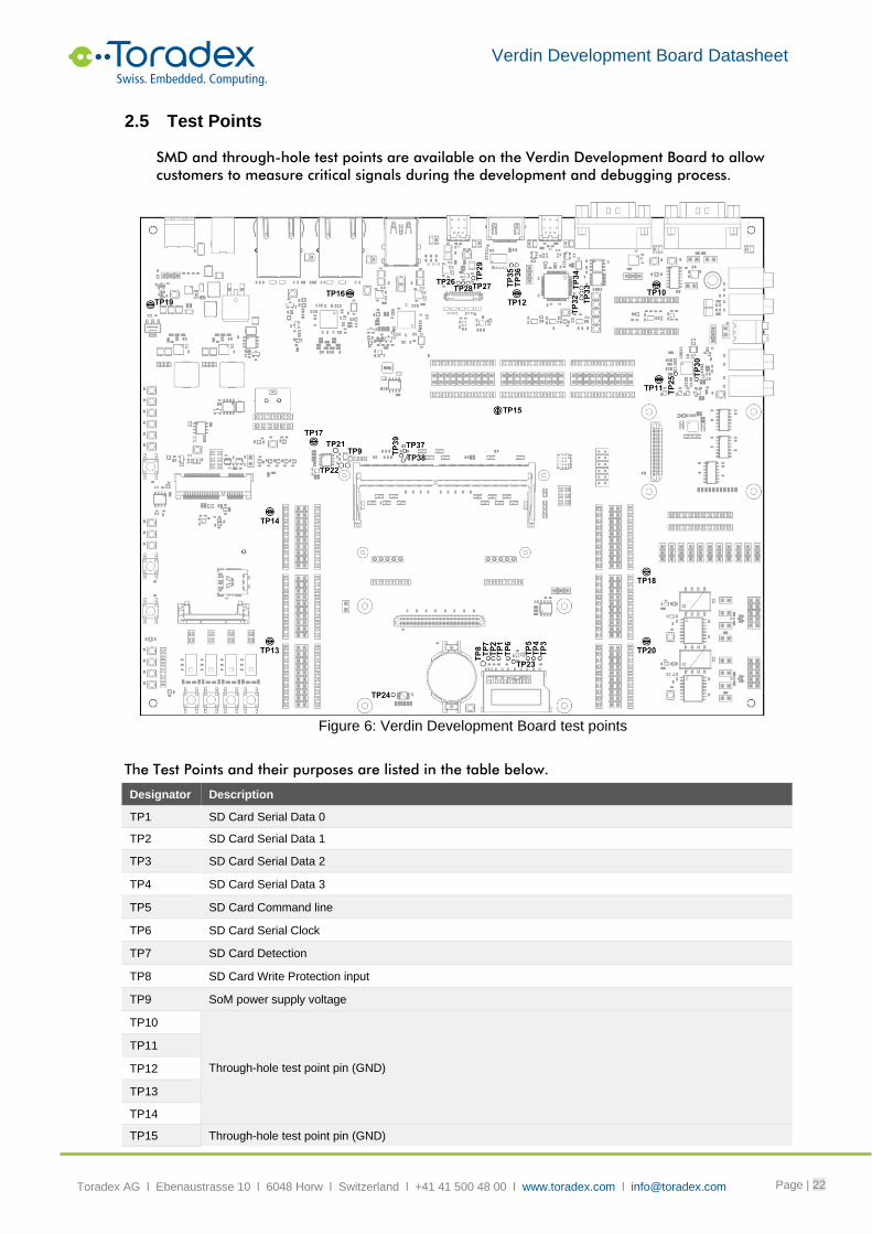
2.5 Test Points
SMD and through-hole test points are available on the Verdin Development Board to allow
customers to measure critical signals during the development and debugging process.
Figure 6: Verdin Development Board test points
The Test Points and their purposes are listed in the table below.
Designator Description
TP1 SD Card Serial Data 0
TP2 SD Card Serial Data 1
TP3 SD Card Serial Data 2
TP4 SD Card Serial Data 3
TP5 SD Card Command line
TP6 SD Card Serial Clock
TP7 SD Card Detection
TP8 SD Card Write Protection input
TP9 SoM power supply voltage
TP10
Through-hole test point pin (GND)
TP11
TP12
TP13
TP14
TP15 Through-hole test point pin (GND)

Verdin Development Board Datasheet
Toradex AG l Ebenaustrasse 10 l 6048 Horw l Switzerland l +41 41 500 48 00 l www.toradex.com l [email protected] Page | 23
Designator Description
TP16
TP17
TP18
TP19
TP20
TP21 SoM power supply current sensing resistor (High side)
TP22 SoM power supply current sensing resistor (Low side)
TP23 SD Card power supply
TP24 Open Drain “ALERT” output of the temperature sensing IC50
TP25 RLIN/GPIO3 pin of the Audio Codec IC28
TP26 Open Drain “VCONN_FAULT” output of the IC53 pulled up to +V1.8_SW with 100k resistor
TP27 Open Drain “OUT2” output of the IC53 for the current mode detection logic
TP28 Open Drain “OUT1” output of the IC53 for the current mode detection logic
TP29 Open Drain “DIR” output of the IC53 for the USB-C plug orientation indication
TP30 CSB/GPIO1 pin of the Audio Codec IC28
TP31 CDBUS2 pin of the universal USB converter IC41 (USB Debugger 3.3V RTS output)
TP32 CDBUS3 pin of the universal USB converter IC41 (USB Debugger 3.3V CTS input)
TP33 DDBUS2 pin of the universal USB converter IC41 (USB Debugger 3.3V RTS output)
TP34 DDBUS3 pin of the universal USB converter IC41 (USB Debugger 3.3V CTS input)
TP35 HDMI eARC differential line positive signal
TP36 HDMI eARC differential line negative signal
TP37 Ethernet_2 transceiver interrupt output. It can be used as a regular GPIO if R332 is removed
TP38 Ethernet_2 transceiver MDIO data signal. It can be used as a regular GPIO if R150 is removed
TP39 Ethernet_2 transceiver MDIO clock signal. It can be used as a regular GPIO if R147 is removed

Verdin Development Board Datasheet
Toradex AG l Ebenaustrasse 10 l 6048 Horw l Switzerland l +41 41 500 48 00 l www.toradex.com l [email protected] Page | 24
2.6 Ethernet Interface
The Verdin Development Board provides 2x RJ45 connectors with integrated magnetics for
10/100/1000Mb Ethernet. The Ethernet_1 transceiver is located on the SoM while the Ethernet_2
transceiver is placed on the Verdin Development Board. Some modules do not feature both
Ethernet interfaces. Please refer to the datasheet of the respective Verdin SoM.
2.6.1 Ethernet_1 Connector (X25)
Connector type: RJ45, BEL A829-1J1T-KM / LINK-PP LPJK7436A98NL
Pin Signal Name SODIMM
Pin I/O Type Voltage Description
1 ETH_1_CTREF_2 Integrated magnetics center tap 2
2 ETH_1_MDI2_N 241 I/O (Analog) Media Dependent Interface
3 ETH_1_MDI2_P 239 I/O (Analog) Media Dependent Interface
4 ETH_1_MDI1_P 233 I/O (Analog) Media Dependent Interface
5 ETH_1_MDI1_N 231 I/O (Analog) Media Dependent Interface
6 ETH_1_CTREF_1 Integrated magnetics center tap 1
7 ETH_1_CTREF_3 Integrated magnetics center tap 3
8 ETH_1_MDI3_P 247 I/O (Analog) Media Dependent Interface
9 ETH_1_MDI3_N 245 I/O (Analog) Media Dependent Interface
10 ETH_1_MDI0_N 227 I/O (Analog) Media Dependent Interface
11 ETH_1_MDI0_P 225 I/O (Analog) Media Dependent Interface
12 ETH_1_CTREF_0 Integrated magnetics center tap 0
13 ETH_1_LED_1_C 235 O (OD) LED for indication Ethernet activity
14 +V3.3_SW PWR +3.3V Power supply for the indication LEDs
15 NC Not Connected
16 +V3.3_SW PWR +3.3V Power supply for the indication LEDs
17 ETH_1_LED_2_C 237 O (OD) LED for indication established Ethernet link
S1/S2 GND_CHASSIS PWR
2.6.2 Ethernet_2 Connector (X35)
The Ethernet_2 interface is based on the KSZ9131RNXI 10/100/1000 Mbps Ethernet PHY which is
using ETH_2_RGMII interface of the module. For more information, refer to the KSZ9131RNX IC
datasheet.
Connector type: RJ45, BEL A829-1J1T-KM / LINK-PP LPJK7436A98NL
Pin Signal Name I/O Type Voltage Description
1 ETH_2_CTREF_2 Integrated magnetics center tap 2
2 ETH_2_MDI2_N I/O (Analog) Media Dependent Interface
3 ETH_2_MDI2_P I/O (Analog) Media Dependent Interface
4 ETH_2_MDI1_P I/O (Analog) Media Dependent Interface
5 ETH_2_MDI1_N I/O (Analog) Media Dependent Interface
6 ETH_2_CTREF_1 Integrated magnetics center tap 1
7 ETH_2_CTREF_3 Integrated magnetics center tap 3
8 ETH_2_MDI3_P I/O (Analog) Media Dependent Interface
9 ETH_2_MDI3_N I/O (Analog) Media Dependent Interface
10 ETH_2_MDI0_N I/O (Analog) Media Dependent Interface
11 ETH_2_MDI0_P I/O (Analog) Media Dependent Interface
12 ETH_2_CTREF_0 Integrated magnetics center tap 0
13 ETH_1_LED_1_C O (OD) LED for indication Ethernet activity
Verdin Development Board Datasheet
Toradex AG l Ebenaustrasse 10 l 6048 Horw l Switzerland l +41 41 500 48 00 l www.toradex.com l [email protected] Page | 25
Pin Signal Name I/O Type Voltage Description
14 +V3.3_SW PWR +3.3V Power supply for the indication LEDs
15 NC Not Connected
16 +V3.3_SW PWR +3.3V Power supply for the indication LEDs
17 ETH_1_LED_2_C O (OD) LED for indication established Ethernet link
S1/S2 GND_CHASSIS PWR
2.7 Verdin USB_1 Port
The Verdin Development Board integrates a USB-C connector X34, connected to the Verdin USB_1
port (USB 2.0 interface only). This port is usually used in the recovery mode for loading new
software onto the module and can work as a dual-role-port (DRP), which means Host or Device.
This behaviour is similar to the On-The-Go (OTG) functionality, but the term USB OTG is only used
in conjunction with the USB Micro-AB or the obsolete USB Mini-AB receptacle. ID pin is absent on
the USB Type-C receptacle. The determination of Host or Device functionality is handled differently
in Type-C using the configuration channel (CC) pins. The CC pins perform the same functions that
the ID pin previously performed: they indicate the role of equipment as host, device, or both. The
CC pins also detect if the connection is being made or if it is broken.
To handle all the operations required for the USB dual-role-port TUSB321AI chip has been used. It
can function as an upstream-facing port (UFP), downstream-facing port (DFP), or a dual-role port
(DRP) product based on a pin configuration. The device handles all aspects of the USB Type-C
connection process (including the CC pins that mirror the micro-A/B ID pin behavior) to determine
the port role. When connected as a peripheral (UFP), the TUSB321AI indicates the VBUS current
provided by the attached host through the general-purpose input/output (GPIO) pins. When
connected as a DFP, these devices advertise VBUS current to the attached peripheral. For the
details, please check the TUSB321AI datasheet.
On the Development Board, this port is configured as a dual-role port (DRP) by default, and its
output current is limited to 1A.
2.7.1 USB_1 Connector (X34)
Connector type: USB-C, Amphenol 12401598E4#2A
Pin Signal Name SODIMM
Pin I/O Type Voltage Description
A1 GND PWR
A2 NC Not Connected
A3 NC Not Connected
A4 +V5_VBUS_USB_1 159 PWR +5V +5V USB power output
A5 USB_1_CC1 Type-C configuration channel signal 1
A6 USB_1_D_CON_P 165 I/O Positive differential USB 2.0 Signal
A7 USB_1_D_CON_N 163 I/O Negative differential USB 2.0 Signal
A8 NC Not Connected
A9 +V5_VBUS_USB_1 159 PWR +5V +5V USB power output
A10 NC Not Connected
A11 NC Not Connected
A12 GND PWR
B1 GND PWR
B2 NC Not Connected
B3 NC Not Connected
B4 +V5_VBUS_USB_1 159 PWR +5V +5V USB power output

Verdin Development Board Datasheet
Toradex AG l Ebenaustrasse 10 l 6048 Horw l Switzerland l +41 41 500 48 00 l www.toradex.com l [email protected] Page | 26
Pin Signal Name SODIMM
Pin I/O Type Voltage Description
B5 USB_1_CC2 Type-C configuration channel signal 1
B6 USB_1_D_CON_P 165 I/O Positive differential USB 2.0 Signal
B7 USB_1_D_CON_N 163 I/O Negative differential USB 2.0 Signal
B8 NC Not Connected
B9 +V5_VBUS_USB_1 159 PWR +5V +5V USB power output
B10 NC Not Connected
B11 NC Not Connected
B12 GND
SH1/SH2 GND_CHASSIS PWR
SH3/SH4 GND_CHASSIS PWR
2.8 Verdin USB_2 Port
The Verdin Development Board integrates a 4 port USB hub (Microchip USB5744T-I/2G) connected
the SoM’s USB_2 port, providing 4x USB 3.x / USB 2.0 Host interfaces. The level of USB 3.x
standard supported depends on the SoM. Some SoMs may not support USB 3.x interface at all.
Refer to the respective SoM datasheet to get the detailed information about supported USB
interfaces and their speed. The hub itself support USB 3.2 Gen 1 / USB 2.0 standards.
The naming schemes of USB 3.x (SuperSpeed) interface can be a bit confusing. There are different
names for the same speed grade, depending on the revision of the specifications that are taken. In
a table below a short comparison of the different transfer modes and their naming schemes has
been done. Not all the USB 3.x transfer modes are possible with the Verdin modules, since in the
Verdin standard only one lane of SuperSpeed signals are reserved.
Marketing Name USB 3.2 Name USB 3.1 Name USB 3.0 Name Nominal Speed
SuperSpeed Lanes
Supported by Verdin
SuperSpeed USB USB 3.2 Gen 1x1 USB 3.1 Gen 1 USB 3.0 5 Gbit/s0.5 GByte/s
1 Possible
SuperSpeed USB 10 Gbit/
USB 3.2 Gen 1x2 10 Gbit/s1 GByte/s
2 No
SuperSpeed USB 10 Gbit/s
USB 3.2 Gen 2x1 USB 3.1 Gen 2 10 Gbit/s1.2 GByte/s
1 Possible
SuperSpeed USB 20 Gbit/s
USB 3.2 Gen 2x2 20 Gbit/s2.4 GByte/s
2 No
The OC sensing pin of the USB_2 port is not used, and the USB hub handles OC conditions. Port 1
of the USB hub is disabled; on Port 4, only the USB 2.0 interface is used, and it is routed to the
Mini PCIe connector (X33). Port 2 and Port 3 are routed to a stacked USB 3.0 Type-A connector
(X53). Maximum data rate for this connector is 5Gbit/s. For further information about the USB hub,
please refer to its datasheet.

Verdin Development Board Datasheet
Toradex AG l Ebenaustrasse 10 l 6048 Horw l Switzerland l +41 41 500 48 00 l www.toradex.com l [email protected] Page | 27
2.8.1 USB_2 Connector (X53)
Connector type: Stacked USB 3.0 Type-A, Amphenol GSB311231HR
(Pins starting with U connect to the UPPER, pins starting with L connect to the LOWER port)
Pin Signal Name I/O Type Voltage Description
U1 +V5_VBUS_USBH3 PWR +5V +5V USB power output
U2 USBH3_CON_D_N I/O Negative differential USB 2.0 signal
U3 USBH3_CON_D_P I/O Positive differential USB 2.0 signal
U4 GND PWR
U5 USBH3_SSRX_CON_N I Negative differential USB 3.x receive signal
U6 USBH3_SSRX_CON_P I Positive differential USB 3.x receive signal
U7 GND PWR
U8 USBH3_SSTX_CON_N O Negative differential USB 3.x transmit signal
U9 USBH3_SSTX_CON_P O Positive differential USB 3.x transmit signal
L1 +V5_VBUS_USBH2 PWR +5V +5V USB power output
L2 USBH2_CON_D_N I/O Negative differential USB 2.0 signal
L3 USBH2_CON_D_P I/O Positive differential USB 2.0 signal
L4 GND PWR
L5 USBH2_SSRX_CON_N I Negative differential USB 3.x receive signal
L6 USBH2_SSRX_CON_P I Positive differential USB 3.x receive signal
L7 GND PWR
L8 USBH2_SSTX_CON_N O Negative differential USB 3.x transmit signal
L9 USBH2_SSTX_CON_P O Positive differential USB 3.x transmit signal
S1/S2 GND_CHASSIS PWR
S3/S4 GND_CHASSIS PWR
2.9 PCIe Interface
The Verdin Development Board makes the standard PCIe interface on the Verdin SoMs available
on a Mini PCIe slot. PCI Express Mini Card is a replacement for the Mini PCI form factor. Mini PCIe
provides both the standard PCI Express and USB 2.0 signals, allowing flexibility in peripheral
design. PCI Express Mini Card edge connectors provide multiple connections and buses, such as
listed below:
• PCI Express 1 lane (with SMBus)
• USB 2.0
• Indication LEDs for wireless network status
• SIM card for cellular applications (UIM signals)
2.9.1 Mini PCIe Connector (X33)
Connector type: Mini PCIe Card Connector and Latch, Molex 67910-5700, 48099-5701
Pin Signal Name SODIMM
Pin I/O Type Voltage
Pull-up/Pull-down
Description
1 PCIE_1_WAKE# 252 O (OD) +1.8V 5.1k to +V1.8_SW Wake-up to SoM
3 NC
Not connected 5 NC
7 NC
9 GND PWR
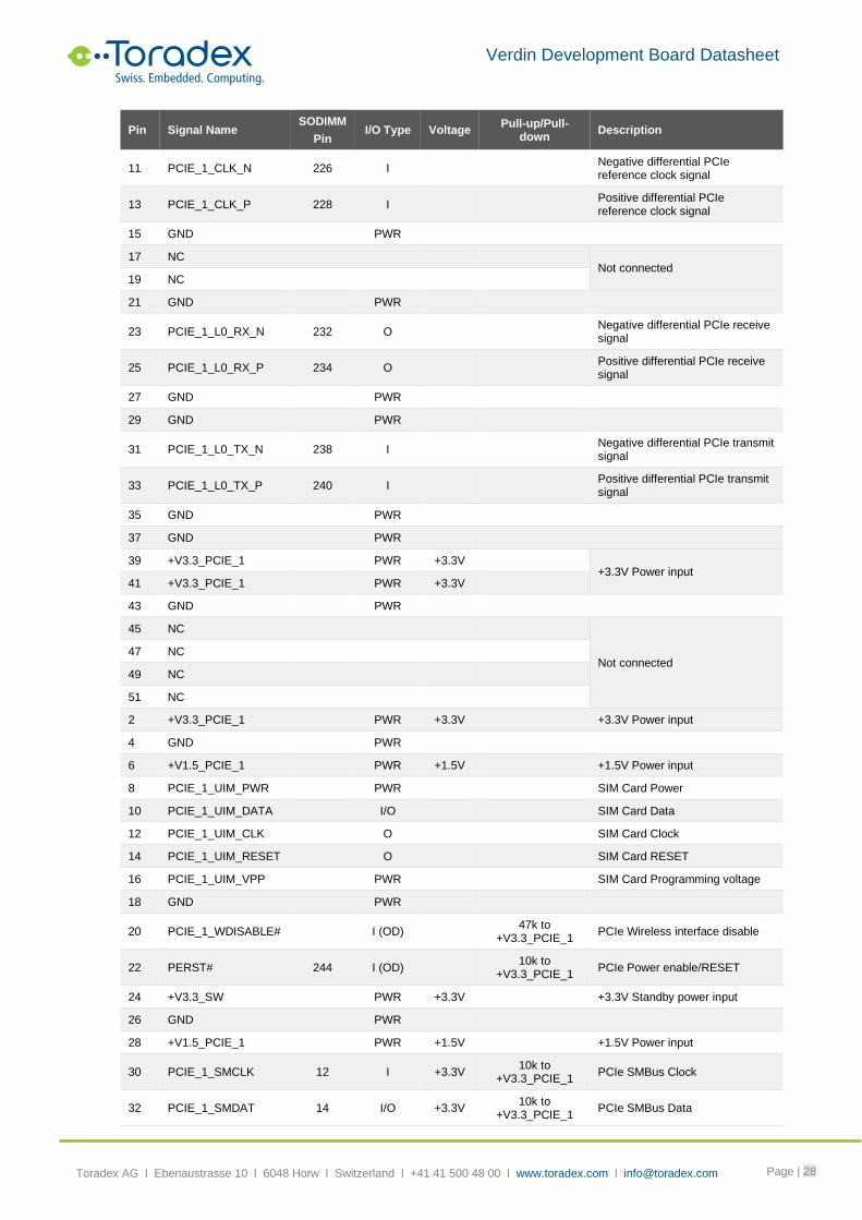
Verdin Development Board Datasheet
Toradex AG l Ebenaustrasse 10 l 6048 Horw l Switzerland l +41 41 500 48 00 l www.toradex.com l [email protected] Page | 28
Pin Signal Name SODIMM
Pin I/O Type Voltage
Pull-up/Pull-down
Description
11 PCIE_1_CLK_N 226 I Negative differential PCIe reference clock signal
13 PCIE_1_CLK_P 228 I Positive differential PCIe reference clock signal
15 GND PWR
17 NC Not connected
19 NC
21 GND PWR
23 PCIE_1_L0_RX_N 232 O Negative differential PCIe receive signal
25 PCIE_1_L0_RX_P 234 O Positive differential PCIe receive signal
27 GND PWR
29 GND PWR
31 PCIE_1_L0_TX_N 238 I Negative differential PCIe transmit signal
33 PCIE_1_L0_TX_P 240 I Positive differential PCIe transmit signal
35 GND PWR
37 GND PWR
39 +V3.3_PCIE_1 PWR +3.3V +3.3V Power input
41 +V3.3_PCIE_1 PWR +3.3V
43 GND PWR
45 NC
Not connected 47 NC
49 NC
51 NC
2 +V3.3_PCIE_1 PWR +3.3V +3.3V Power input
4 GND PWR
6 +V1.5_PCIE_1 PWR +1.5V +1.5V Power input
8 PCIE_1_UIM_PWR PWR SIM Card Power
10 PCIE_1_UIM_DATA I/O SIM Card Data
12 PCIE_1_UIM_CLK O SIM Card Clock
14 PCIE_1_UIM_RESET O SIM Card RESET
16 PCIE_1_UIM_VPP PWR SIM Card Programming voltage
18 GND PWR
20 PCIE_1_WDISABLE# I (OD) 47k to
+V3.3_PCIE_1 PCIe Wireless interface disable
22 PERST# 244 I (OD) 10k to
+V3.3_PCIE_1 PCIe Power enable/RESET
24 +V3.3_SW PWR +3.3V +3.3V Standby power input
26 GND PWR
28 +V1.5_PCIE_1 PWR +1.5V +1.5V Power input
30 PCIE_1_SMCLK 12 I +3.3V 10k to
+V3.3_PCIE_1 PCIe SMBus Clock
32 PCIE_1_SMDAT 14 I/O +3.3V 10k to
+V3.3_PCIE_1 PCIe SMBus Data

Verdin Development Board Datasheet
Toradex AG l Ebenaustrasse 10 l 6048 Horw l Switzerland l +41 41 500 48 00 l www.toradex.com l [email protected] Page | 29
Pin Signal Name SODIMM
Pin I/O Type Voltage
Pull-up/Pull-down
Description
34 GND PWR
36 USBH4_D_N I/O Negative differential USB 2.0 data signal
38 USBH4_D_P I/O Positive differential USB 2.0 data signal
40 GND PWR
42 PCIE_1_WWAN# O (OD) WWAN LED
44 PCIE_1_WLAN# O (OD) WLAN LED
46 PCIE_1_WPAN# O (OD) WPAN LED
48 +V1.5_PCIE_1 PWR +1.5V +1.5V Power input
50 GND PWR
52 +V3.3_PCIE_1 PWR +3.3V +3.3V Power input
2.9.2 SIM Card Holder (X36)
Connector type: NANO SIM, Molex 1042240820
Pin Signal Name I/O Type Voltage Pull-up/Pull-down Description
S1 PCIE1_B_UIM_PWR PWR SIM Card Power
S2 PCIE1_B_UIM_RESET I SIM Card RESET
S3 PCIE1_B_UIM_CLK I SIM Card Clock
S4 GND PWR
S5 PCIE1_B_UIM_VPP PWR SIM Card Programming voltage
S6 PCIE1_B_UIM_DATA I/O SIM Card Data
G1/G2 GND PWR
G3/G4 GND PWR
Verdin Development Board Datasheet
Toradex AG l Ebenaustrasse 10 l 6048 Horw l Switzerland l +41 41 500 48 00 l www.toradex.com l [email protected] Page | 30
2.10 SD Card Interface
The Verdin Development Board has a 4-bit SDIO interface and a hardware-supported card
detection function (CD). SD Card write-protection status can be verified using the related test point
on the board. The Verdin family supports SD Card Low Voltage Signalling mode. So, if the SD card
itself also supports this mode, then communication will start at 3.3V and switch to 1.8V after the
card has been initialized.
The SD_1_PWR_EN signal allows to power ON and OFF SD the Card power supply (+V3.3_SD).
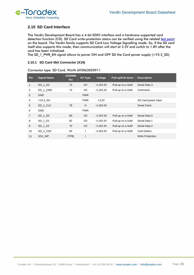
2.10.1 SD Card 4bit Connector (X19)
Connector type: SD Card, Würth 693063020911
Pin Signal Name SODIMM
Pin I/O Type Voltage Pull-up/Pull-down Description
1 SD_1_D3 72 I/O +1.8/3.3V Pull-up on a SoM Serial Data 3
2 SD_1_CMD 74 I/O +1.8/3.3V Pull-up on a SoM Command
3 GND PWR
4 +V3.3_SD PWR +3.3V SD Card power input
5 SD_1_CLK 78 O +1.8/3.3V Serial Clock
6 GND PWR
7 SD_1_D0 80 I/O +1.8/3.3V Pull-up on a SoM Serial Data 0
8 SD_1_D1 82 I/O +1.8/3.3V Pull-up on a SoM Serial Data 1
9 SD_1_D2 70 I/O +1.8/3.3V Pull-up on a SoM Serial Data 2
10 SD_1_CD# 84 I +1.8/3.3V Pull-up on a SoM Card Detect
11 SD1_WP (TP8) I Write Protection
Verdin Development Board Datasheet
Toradex AG l Ebenaustrasse 10 l 6048 Horw l Switzerland l +41 41 500 48 00 l www.toradex.com l [email protected] Page | 31
2.11 Display Interface
The Verdin Development Board provides two options for connecting LCD panels and monitors via
the following two interfaces supported:
• HDMI
• MIPI DSI
Almost any TFT display can be connected to the Verdin module by HDMI port X37 or via the DSI
interface connector X48. X48 features a universal mezzanine board connector. This solution allows
for connecting various types of display interface mezzanine boards and converters, e.g., DSI to
HDMI, DSI to LVDS, DSI to RGB, etc. Custom boards with the appropriate MIPI DSI connector can
also be used.
2.11.1 HDMI Connector (X11)
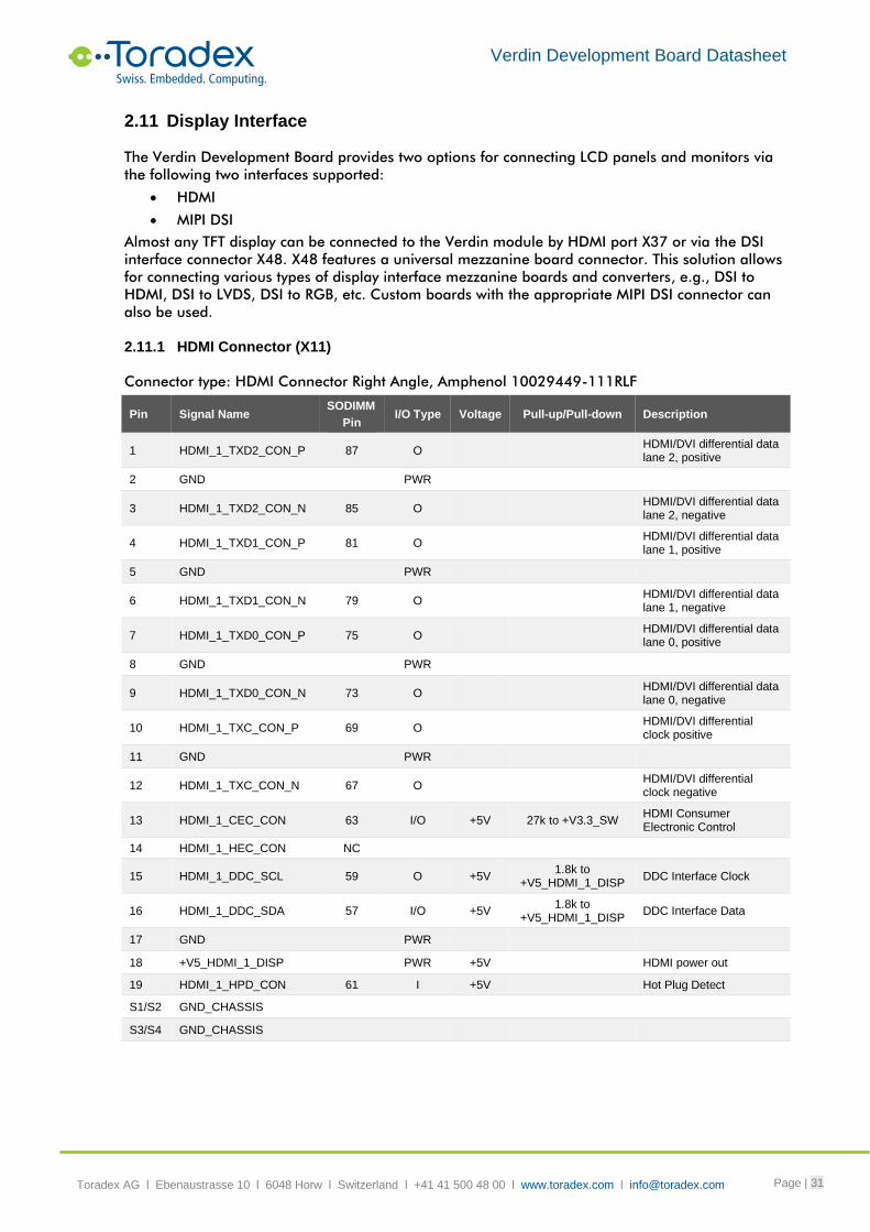
Connector type: HDMI Connector Right Angle, Amphenol 10029449-111RLF
Pin Signal Name SODIMM
Pin I/O Type Voltage Pull-up/Pull-down Description
1 HDMI_1_TXD2_CON_P 87 O HDMI/DVI differential data lane 2, positive
2 GND PWR
3 HDMI_1_TXD2_CON_N 85 O HDMI/DVI differential data lane 2, negative
4 HDMI_1_TXD1_CON_P 81 O HDMI/DVI differential data lane 1, positive
5 GND PWR
6 HDMI_1_TXD1_CON_N 79 O HDMI/DVI differential data lane 1, negative
7 HDMI_1_TXD0_CON_P 75 O HDMI/DVI differential data lane 0, positive
8 GND PWR
9 HDMI_1_TXD0_CON_N 73 O HDMI/DVI differential data lane 0, negative
10 HDMI_1_TXC_CON_P 69 O HDMI/DVI differential clock positive
11 GND PWR
12 HDMI_1_TXC_CON_N 67 O HDMI/DVI differential clock negative
13 HDMI_1_CEC_CON 63 I/O +5V 27k to +V3.3_SW HDMI Consumer Electronic Control
14 HDMI_1_HEC_CON NC
15 HDMI_1_DDC_SCL 59 O +5V 1.8k to
+V5_HDMI_1_DISP DDC Interface Clock
16 HDMI_1_DDC_SDA 57 I/O +5V 1.8k to
+V5_HDMI_1_DISP DDC Interface Data
17 GND PWR
18 +V5_HDMI_1_DISP PWR +5V HDMI power out
19 HDMI_1_HPD_CON 61 I +5V Hot Plug Detect
S1/S2 GND_CHASSIS
S3/S4 GND_CHASSIS
Verdin Development Board Datasheet
Toradex AG l Ebenaustrasse 10 l 6048 Horw l Switzerland l +41 41 500 48 00 l www.toradex.com l [email protected] Page | 32
2.11.2 DSI Display Adapter Connector (X48)
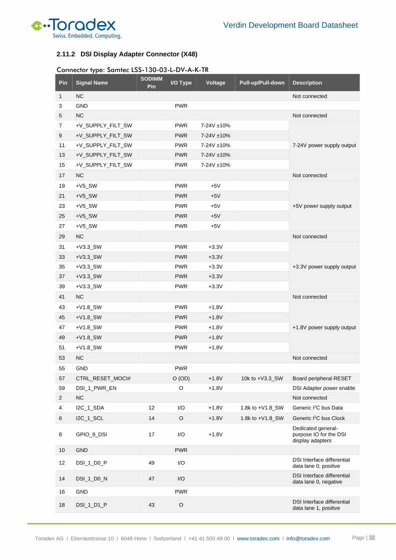
Connector type: Samtec LSS-130-03-L-DV-A-K-TR
Pin Signal Name SODIMM
Pin I/O Type Voltage Pull-up/Pull-down Description
1 NC Not connected
3 GND PWR
5 NC Not connected
7 +V_SUPPLY_FILT_SW PWR 7-24V ±10%
7-24V power supply output
9 +V_SUPPLY_FILT_SW PWR 7-24V ±10%
11 +V_SUPPLY_FILT_SW PWR 7-24V ±10%
13 +V_SUPPLY_FILT_SW PWR 7-24V ±10%
15 +V_SUPPLY_FILT_SW PWR 7-24V ±10%
17 NC Not connected
19 +V5_SW PWR +5V
+5V power supply output
21 +V5_SW PWR +5V
23 +V5_SW PWR +5V
25 +V5_SW PWR +5V
27 +V5_SW PWR +5V
29 NC Not connected
31 +V3.3_SW PWR +3.3V
+3.3V power supply output
33 +V3.3_SW PWR +3.3V
35 +V3.3_SW PWR +3.3V
37 +V3.3_SW PWR +3.3V
39 +V3.3_SW PWR +3.3V
41 NC Not connected
43 +V1.8_SW PWR +1.8V
+1.8V power supply output
45 +V1.8_SW PWR +1.8V
47 +V1.8_SW PWR +1.8V
49 +V1.8_SW PWR +1.8V
51 +V1.8_SW PWR +1.8V
53 NC Not connected
55 GND PWR
57 CTRL_RESET_MOCI# O (OD) +1.8V 10k to +V3.3_SW Board peripheral RESET
59 DSI_1_PWR_EN O +1.8V DSI Adapter power enable
2 NC Not connected
4 I2C_1_SDA 12 I/O +1.8V 1.8k to +V1.8_SW Generic I2C bus Data
6 I2C_1_SCL 14 O +1.8V 1.8k to +V1.8_SW Generic I2C bus Clock
8 GPIO_9_DSI 17 I/O +1.8V Dedicated general-purpose IO for the DSI display adapters
10 GND PWR
12 DSI_1_D0_P 49 I/O DSI Interface differential data lane 0, positive
14 DSI_1_D0_N 47 I/O DSI Interface differential data lane 0, negative
16 GND PWR
18 DSI_1_D1_P 43 O DSI Interface differential data lane 1, positive
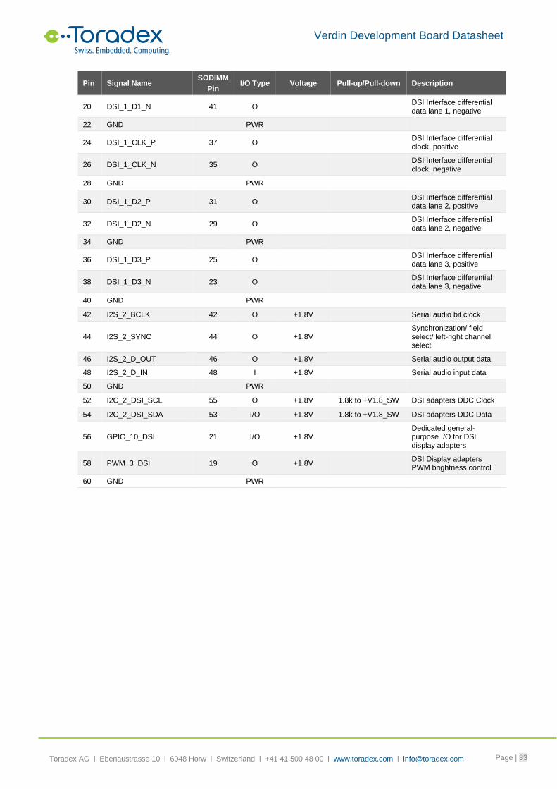
Verdin Development Board Datasheet
Toradex AG l Ebenaustrasse 10 l 6048 Horw l Switzerland l +41 41 500 48 00 l www.toradex.com l [email protected] Page | 33
Pin Signal Name SODIMM
Pin I/O Type Voltage Pull-up/Pull-down Description
20 DSI_1_D1_N 41 O DSI Interface differential data lane 1, negative
22 GND PWR
24 DSI_1_CLK_P 37 O DSI Interface differential clock, positive
26 DSI_1_CLK_N 35 O DSI Interface differential clock, negative
28 GND PWR
30 DSI_1_D2_P 31 O DSI Interface differential data lane 2, positive
32 DSI_1_D2_N 29 O DSI Interface differential data lane 2, negative
34 GND PWR
36 DSI_1_D3_P 25 O DSI Interface differential data lane 3, positive
38 DSI_1_D3_N 23 O DSI Interface differential data lane 3, negative
40 GND PWR
42 I2S_2_BCLK 42 O +1.8V Serial audio bit clock
44 I2S_2_SYNC 44 O +1.8V Synchronization/ field select/ left-right channel select
46 I2S_2_D_OUT 46 O +1.8V Serial audio output data
48 I2S_2_D_IN 48 I +1.8V Serial audio input data
50 GND PWR
52 I2C_2_DSI_SCL 55 O +1.8V 1.8k to +V1.8_SW DSI adapters DDC Clock
54 I2C_2_DSI_SDA 53 I/O +1.8V 1.8k to +V1.8_SW DSI adapters DDC Data
56 GPIO_10_DSI 21 I/O +1.8V Dedicated general-purpose I/O for DSI display adapters
58 PWM_3_DSI 19 O +1.8V DSI Display adapters PWM brightness control
60 GND PWR
Verdin Development Board Datasheet
Toradex AG l Ebenaustrasse 10 l 6048 Horw l Switzerland l +41 41 500 48 00 l www.toradex.com l [email protected] Page | 34
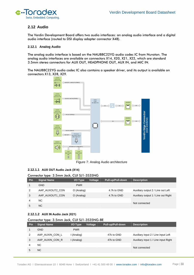
2.12 Audio
The Verdin Development Board offers two audio interfaces: an analog audio interface and a digital
audio interface (routed to DSI display adapter connector X48).
2.12.1 Analog Audio
The analog audio interface is based on the NAU88C22YG audio codec IC from Nuvoton. The
analog audio interfaces are available on connectors X14, X20, X21, X22, which are standard
3.5mm stereo connectors for AUX OUT, HEADPHONE OUT, AUX IN, and MIC IN.
The NAU88C22YG audio codec IC also contains a speaker driver, and its output is available on
connectors X13, X28, X29.
JUM PERS
JUM PERS
Audio
Codec
NA U88C22YG
O n-board
M icrophone MI C1
CMEJ-0706-42-P
Speak er
Connector X28
3.5mm
Audio Jack
Connector X22
3.5mm
Audio Jack
Connector X20
3.5mm
Audio Jack
Connector X21
3.5mm
Audio Jack
Connector X14
AU X O UT / LIN E O UT (STEREO)
AU X I N / LIN E IN (S TEREO )
HP O UT (STEREO)
M IC IN (STEREO)
M IC OU T
SPEAKER O UT (STEREO/BTL)
I2C
I2S
3-pin
M ale H ea der
X13
Ve
rdin
Ed
ge C
on
ne
cto
r(D
D4
SO
DIM
M)
I2C I2C
I2S
2-pin
M ale H ea der
X29
Figure 7: Analog Audio architecture
2.12.1.1 AUX OUT Audio Jack (X14)
Connector type: 3.5mm Jack, CUI SJ1-3535NG
Pin Signal Name I/O Type Voltage Pull-up/Pull-down Description
1 GND PWR
2 AAP_AUXOUT2_CON O (Analog) 4.7k to GND Auxiliary output 2 / Line out Left
3 AAP_AUXOUT1_CON O (Analog) 4.7k to GND Auxiliary output 1 / Line out Right
4 NC Not connected
5 NC
2.12.1.2 AUX IN Audio Jack (X21)
Connector type: 3.5mm Jack, CUI SJ1-3535NG-BE
Pin Signal Name I/O Type Voltage Pull-up/Pull-down Description
1 GND PWR
2 AAP_AUXIN_CON_L I (Analog) 47k to GND Auxiliary input 2 / Line input Left
3 AAP_AUXIN_CON_R I (Analog) 47k to GND Auxiliary input 1 / Line input Right
4 NC Not connected
5 NC
Verdin Development Board Datasheet
Toradex AG l Ebenaustrasse 10 l 6048 Horw l Switzerland l +41 41 500 48 00 l www.toradex.com l [email protected] Page | 35
2.12.1.3 HEADPHONES OUT Audio Jack (X20)
Connector type: 3.5mm Jack, CUI SJ1-3535NG-GR
Pin Signal Name I/O Type Voltage Pull-up/Pull-down Description
1 GND PWR
2 AAP_HP_CON_L O (Analog) 10k to GND Headphones output Left
3 AAP_HP_CON_R O (Analog) 10k to GND Headphones output Right
4 NC Not connected Not connected
5 AAP_LLIN_CON_GPIO2 +1.8V 47k to +V1.8_AAP_VDDB Headphones connect detection
2.12.1.4 MIC IN Audio Jack (X22)
Connector type: 3.5mm Jack, CUI SJ1-3535NG-PI
Pin Signal Name I/O Type Voltage Pull-up/Pull-down Description
1 GND PWR
2 AAP_LMIC_CON_P I 2.2k to AAP_MICBIAS Microphone input Left
3 AAP_RMIC_CON_P I 2.2k to AAP_MICBIAS Microphone input Right
4 AAP_MIC_1_OUT O On-board microphone output
5 GND PWR
Microphone MIC1, located on the board, can be used when the external microphone is
disconnected.
2.12.1.5 SPEAKER OUT 2-pin header (X22)
Connector type: 1x3 Pin Header Male, 2.54 mm pitch
Pin Signal Name I/O Type Voltage Pull-up/Pull-down Description
1 AAP_SPKOUT_CON_R O 47k to GND Right speaker output
2 GND PWR
3 AAP_SPKOUT_CON_L O 47k to GND Left speaker output
2.12.1.6 SPEAKER OUT 3-pin header (X29)
Connector type: 1x2 Pin Header Male, 2.54 mm pitch
Pin Signal Name I/O Type Voltage Pull-up/Pull-down Description
1 AAP_SPKOUT_R O BTL1 Speaker Positive Output
2 AAP_SPKOUT_L O BTL1 Speaker Negative Output
2.12.1.7 SPEAKER OUT Connector (X28)
Connector type: 1x2 Terminal block, CUI TBLH10-500-02BK
Pin Signal Name I/O Type Voltage Pull-up/Pull-down Description
1 AAP_SPKOUT_R O BTL1 Speaker Positive Output
2 AAP_SPKOUT_L O BTL1 Speaker Negative Output
1: BTL – Bridge-Tied-Load speaker output configuration. The two channels of a stereo amplifier are fed the same monaural audio signal, with one channel’s electrical polarity reversed. A loudspeaker is connected between the two amplifier outputs, bridging the output terminals. This doubles the available voltage swing at the load compared with the same amplifier used without bridging.
2.12.2 Digital Audio
Digital audio on the Verdin Development Board is available as an I2S interface (I
2S_2). It is
provided on the X48 connector (MIPI DSI interface) to provide the option of using an audio
interface along with display solutions. For detailed information, refer to the X48 connector pinout.

Verdin Development Board Datasheet
Toradex AG l Ebenaustrasse 10 l 6048 Horw l Switzerland l +41 41 500 48 00 l www.toradex.com l [email protected] Page | 36
2.13 “Module-specific” Interface
The “Module-specific” mezzanine board connector provides access to the “Module-specific”
interfaces on the Verdin SoM. The range of available interfaces depends on the Verdin module
being used. For this reason, “Module-specific” (MSP) signals can be both differential pairs or
single-ended signals. All potential differential signals are routed as differential lines with
impedance control (100 Ohm for differential and 55 Ohm for single-ended) and equal length. This
allows them to be used for any high-speed interface a module may provide.
“Module-specific” mezzanine boards are available for most Verdin SoMs and are connected to this
interface to provide access to the “Module-specific” features of those SoMs. Please refer to the
datasheets of the individual “Module-specific” mezzanine boards and respective Verdin SoMs for
more information.
Customers are free to develop their own “Module-specific” mezzanine boards for prototyping and
development purposes. If high-speed differential signals available on MSP pins are used in a
custom application, then stitching capacitors should be placed on single-ended MSP signal lines
(please check the schematic of the Verdin Development Board). The stitching capacitors provide a
return path for the MSP differential signal’s currents, improving signal integrity and reducing EMI.
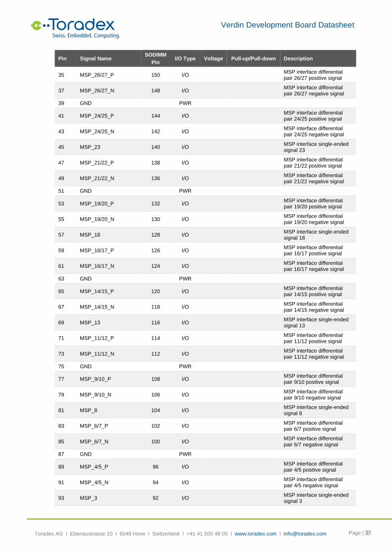
2.13.1 “Module-specific” Mezzanine Board Connector (X52)
Connector type: Samtec LSS-150-03-L-DV-A-K-TR
Pin Signal Name SODIMM
Pin I/O Type Voltage Pull-up/Pull-down Description
1 PWR_1V8_MOCI 214 PWR +1.8V +1.8V SoM power output, 250 mA max
3 GND PWR
5 MSP_39/40_P 180 I/O MSP interface differential pair 39/40 positive signal
7 MSP_39/40_N 178 I/O MSP interface differential pair 39/40 negative signal
9 MSP_38 176 I/O MSP interface single-ended signal 38
11 MSP_36/37_P 174 I/O MSP interface differential pair 36/37 positive signal
13 MSP_36/37_N 172 I/O MSP interface differential pair 36/37 negative signal
15 GND PWR
17 MSP_34/35_P 168 I/O MSP interface differential pair 34/35 positive signal
19 MSP_34/35_N 166 I/O MSP interface differential pair 34/35 negative signal
21 MSP_33 164 I/O MSP interface single-ended signal 33
23 MSP_31/32_P 162 I/O MSP interface differential pair 31/32 positive signal
25 MSP_31/32_N 160 I/O MSP interface differential pair 31/32 negative signal
27 GND PWR
29 MSP_29/30_P 156 I/O MSP interface differential pair 29/30 positive signal
31 MSP_29/30_N 154 I/O MSP interface differential pair 29/30 negative signal
33 MSP_28 152 I/O MSP interface single-ended signal 28
Verdin Development Board Datasheet
Toradex AG l Ebenaustrasse 10 l 6048 Horw l Switzerland l +41 41 500 48 00 l www.toradex.com l [email protected] Page | 37
Pin Signal Name SODIMM
Pin I/O Type Voltage Pull-up/Pull-down Description
35 MSP_26/27_P 150 I/O MSP interface differential pair 26/27 positive signal
37 MSP_26/27_N 148 I/O MSP interface differential pair 26/27 negative signal
39 GND PWR
41 MSP_24/25_P 144 I/O MSP interface differential pair 24/25 positive signal
43 MSP_24/25_N 142 I/O MSP interface differential pair 24/25 negative signal
45 MSP_23 140 I/O MSP interface single-ended signal 23
47 MSP_21/22_P 138 I/O MSP interface differential pair 21/22 positive signal
49 MSP_21/22_N 136 I/O MSP interface differential pair 21/22 negative signal
51 GND PWR
53 MSP_19/20_P 132 I/O MSP interface differential pair 19/20 positive signal
55 MSP_19/20_N 130 I/O MSP interface differential pair 19/20 negative signal
57 MSP_18 128 I/O MSP interface single-ended signal 18
59 MSP_16/17_P 126 I/O MSP interface differential pair 16/17 positive signal
61 MSP_16/17_N 124 I/O MSP interface differential pair 16/17 negative signal
63 GND PWR
65 MSP_14/15_P 120 I/O MSP interface differential pair 14/15 positive signal
67 MSP_14/15_N 118 I/O MSP interface differential pair 14/15 negative signal
69 MSP_13 116 I/O MSP interface single-ended signal 13
71 MSP_11/12_P 114 I/O MSP interface differential pair 11/12 positive signal
73 MSP_11/12_N 112 I/O MSP interface differential pair 11/12 negative signal
75 GND PWR
77 MSP_9/10_P 108 I/O MSP interface differential pair 9/10 positive signal
79 MSP_9/10_N 106 I/O MSP interface differential pair 9/10 negative signal
81 MSP_8 104 I/O MSP interface single-ended signal 8
83 MSP_6/7_P 102 I/O MSP interface differential pair 6/7 positive signal
85 MSP_6/7_N 100 I/O MSP interface differential pair 6/7 negative signal
87 GND PWR
89 MSP_4/5_P 96 I/O MSP interface differential pair 4/5 positive signal
91 MSP_4/5_N 94 I/O MSP interface differential pair 4/5 negative signal
93 MSP_3 92 I/O MSP interface single-ended signal 3

Verdin Development Board Datasheet
Toradex AG l Ebenaustrasse 10 l 6048 Horw l Switzerland l +41 41 500 48 00 l www.toradex.com l [email protected] Page | 38
Pin Signal Name SODIMM
Pin I/O Type Voltage Pull-up/Pull-down Description
95 MSP_1/2_P 90 I/O MSP interface differential pair 1/2 positive signal
97 MSP_1/2_N 88 I/O MSP interface differential pair 1/2 negative signal
99 GND PWR
2 GND PWR
4 MSP_44/45_P 192 I/O MSP interface differential pair 44/45 positive signal
6 MSP_44/45_N 190 I/O MSP interface differential pair 44/45 negative signal
8 MSP_43 188 I/O MSP interface single-ended signal 43
10 MSP_41/42_P 186 I/O MSP interface differential pair 41/42 positive signal
12 MSP_41/42_N 184 I/O MSP interface differential pair 41/42 negative signal
14 GND PWR
16 I2C_4_CSI_SCL 95 O +1.8V 1.8k to +V1.8_SW CSI Camera I2C bus Clock
18 I2C_4_CSI_SDA 93 I/O +1.8V 1.8k to +V1.8_SW CSI Camera I2C bus Data
20 SODIMM_222 (GPIO_8_CSI)
222 I/O +1.8V
General-purpose I/Os, dedicated for the MIPI CSI camera interface
22 SODIMM_220 (GPIO_7_CSI)
220 I/O +1.8V
24 SODIMM_218 (GPIO_6_CSI)
218 I/O +1.8V
26 SODIMM_216 (GPIO_5_CSI)
216 I/O +1.8V
28 GPIO_4 212 I/O +1.8V General-purpose I/O
30 GPIO_3 210 I/O +1.8V General-purpose I/O
32 GPIO_2 208 I/O +1.8V General-purpose I/O
34 GPIO_1 206 I/O +1.8V General-purpose I/O
36 MSP_CSI_1_MCLK 91 O +1.8V CSI camera master clock
38 CTRL_RESET_MOCI# 258 O (OD) +3.3V 10k to +V3.3_SW General reset signal
40 CTRL_SLEEP_MOCI# 256 O +1.8V
42 CTRL_PWR_EN_MOCI 254 O +1.8V General power enable signal
44 CTRL_WAKE1_MICO# 252 I +1.8V 5.1k to +V1.8_SW
46 SPI_1_CS 202 O +1.8V SPI Slave Select
48 SPI_1_MOSI 200 O +1.8V SPI Master Output, Slave Input
50 SPI_1_MISO 198 I +1.8V SPI Master Input, Slave Output
52 SPI_1_CLK 196 O +1.8V SPI Serial Clock
54 I2C_1_SCL 14 O +1.8V 1.8k to +V1.8_SW Generic I2C bus Clock
56 I2C_1_SDA 12 I/O 1.8k to +V1.8_SW Generic I2C bus Data
58 PWR_CTRL_10 O +1.8V MSP mezzanine board power enable
60 +V1.8_SW PWR +1.8V +1.8V power supply output
62 +V1.8_SW PWR +1.8V
64 +V3.3_SW PWR +3.3V +3.3V power supply output
66 +V3.3_SW PWR +3.3V
68 +V5_SW PWR +5V +5V power supply output
70 +V5_SW PWR +5V
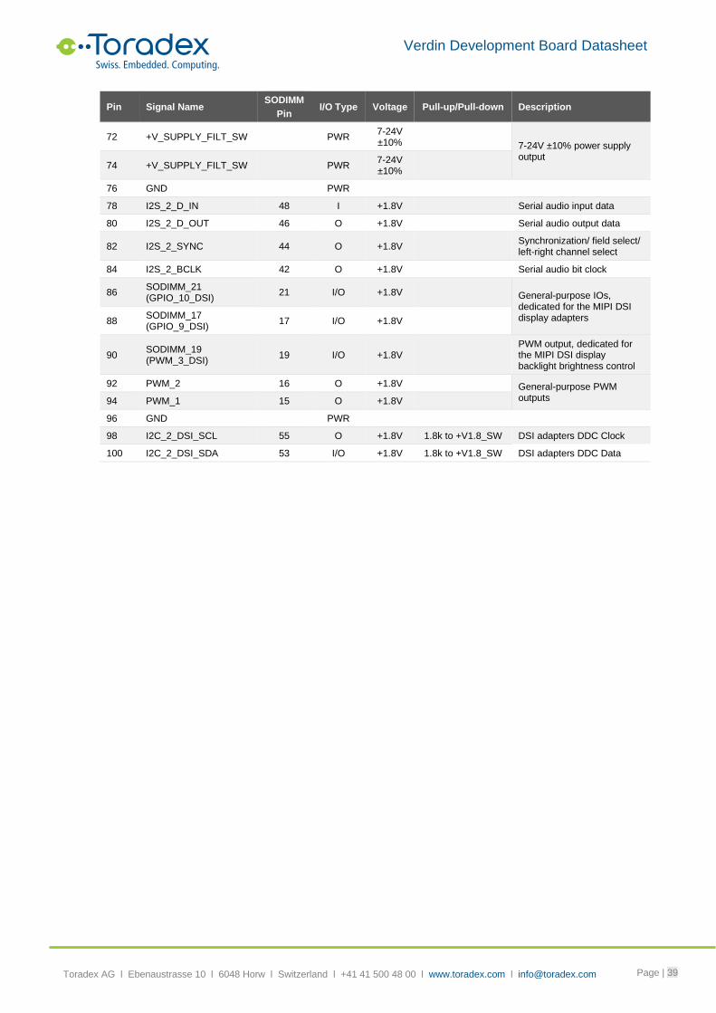
Verdin Development Board Datasheet
Toradex AG l Ebenaustrasse 10 l 6048 Horw l Switzerland l +41 41 500 48 00 l www.toradex.com l [email protected] Page | 39
Pin Signal Name SODIMM
Pin I/O Type Voltage Pull-up/Pull-down Description
72 +V_SUPPLY_FILT_SW PWR 7-24V ±10%
7-24V ±10% power supply output
74 +V_SUPPLY_FILT_SW PWR 7-24V ±10%
76 GND PWR
78 I2S_2_D_IN 48 I +1.8V Serial audio input data
80 I2S_2_D_OUT 46 O +1.8V Serial audio output data
82 I2S_2_SYNC 44 O +1.8V Synchronization/ field select/ left-right channel select
84 I2S_2_BCLK 42 O +1.8V Serial audio bit clock
86 SODIMM_21 (GPIO_10_DSI)
21 I/O +1.8V General-purpose IOs, dedicated for the MIPI DSI display adapters 88
SODIMM_17 (GPIO_9_DSI)
17 I/O +1.8V
90 SODIMM_19 (PWM_3_DSI)
19 I/O +1.8V PWM output, dedicated for the MIPI DSI display backlight brightness control
92 PWM_2 16 O +1.8V General-purpose PWM outputs 94 PWM_1 15 O +1.8V
96 GND PWR
98 I2C_2_DSI_SCL 55 O +1.8V 1.8k to +V1.8_SW DSI adapters DDC Clock
100 I2C_2_DSI_SDA 53 I/O +1.8V 1.8k to +V1.8_SW DSI adapters DDC Data
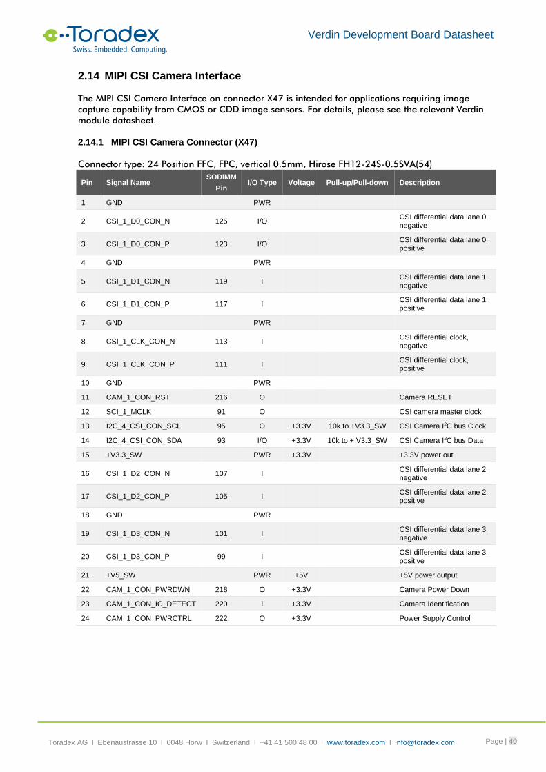
Verdin Development Board Datasheet
Toradex AG l Ebenaustrasse 10 l 6048 Horw l Switzerland l +41 41 500 48 00 l www.toradex.com l [email protected] Page | 40
2.14 MIPI CSI Camera Interface
The MIPI CSI Camera Interface on connector X47 is intended for applications requiring image
capture capability from CMOS or CDD image sensors. For details, please see the relevant Verdin
module datasheet.
2.14.1 MIPI CSI Camera Connector (X47)
Connector type: 24 Position FFC, FPC, vertical 0.5mm, Hirose FH12-24S-0.5SVA(54)
Pin Signal Name SODIMM
Pin I/O Type Voltage Pull-up/Pull-down Description
1 GND PWR
2 CSI_1_D0_CON_N 125 I/O CSI differential data lane 0, negative
3 CSI_1_D0_CON_P 123 I/O CSI differential data lane 0, positive
4 GND PWR
5 CSI_1_D1_CON_N 119 I CSI differential data lane 1, negative
6 CSI_1_D1_CON_P 117 I CSI differential data lane 1, positive
7 GND PWR
8 CSI_1_CLK_CON_N 113 I CSI differential clock, negative
9 CSI_1_CLK_CON_P 111 I CSI differential clock, positive
10 GND PWR
11 CAM_1_CON_RST 216 O Camera RESET
12 SCI_1_MCLK 91 O CSI camera master clock
13 I2C_4_CSI_CON_SCL 95 O +3.3V 10k to +V3.3_SW CSI Camera I2C bus Clock
14 I2C_4_CSI_CON_SDA 93 I/O +3.3V 10k to + V3.3_SW CSI Camera I2C bus Data
15 +V3.3_SW PWR +3.3V +3.3V power out
16 CSI_1_D2_CON_N 107 I CSI differential data lane 2, negative
17 CSI_1_D2_CON_P 105 I CSI differential data lane 2, positive
18 GND PWR
19 CSI_1_D3_CON_N 101 I CSI differential data lane 3, negative
20 CSI_1_D3_CON_P 99 I CSI differential data lane 3, positive
21 +V5_SW PWR +5V +5V power output
22 CAM_1_CON_PWRDWN 218 O +3.3V Camera Power Down
23 CAM_1_CON_IC_DETECT 220 I +3.3V Camera Identification
24 CAM_1_CON_PWRCTRL 222 O +3.3V Power Supply Control

Verdin Development Board Datasheet
Toradex AG l Ebenaustrasse 10 l 6048 Horw l Switzerland l +41 41 500 48 00 l www.toradex.com l [email protected] Page | 41
2.15 Digital and Analog I/O
2.15.1 Communication Interface
2.15.1.1 CAN
The Verdin Development Board uses the Texas Instruments isolated ISO1042BDWR CAN
transceiver to implement two CAN FD interfaces in conjunction with the two CAN interface on the
Verdin module.
CAN ports are electrically isolated from the system power supply and provide an isolated 5V power
supply output with a load capacity of 126 mA for each port.
The CAN interfaces are available on connectors X59 and X60. Pin header-to-DSUB9 adapters can
be used with X59, X60 connectors.
The jumpers JP1, JP2, JP3, JP4 provide hardware configuration for these interfaces:
Connector type: 1x2 Pin Header Male, 2.54 mm pitch
Jumper Status Function
JP1, JP2 CLOSED CAN1 split terminated.
JP3, JP4 CLOSED CAN2 split terminated.
By default, the jumpers JP1, JP2, JP3, JP4 are closed.
2.15.1.1.1 CAN1 Connector (X59)
Connector type: 2x5 Pin Header Male, 2.54 mm pitch
Pin Signal Name I/O Type Voltage Description
1 NC Not connected
2 CAN_1_PGND PWR CAN_1 isolated GND
3 CAN_1_L I/O Low-level CAN_1 bus line
4 CAN_1_H I/O High-level CAN_1 bus line
5 GND_CAN_1_ISO Connected through 100 Ohm
6 NC Not connected
7 NC
8 CAN_1_PWR PWR +5V CAN_1 isolated power out
9 NC Not connected
10 NC
2.15.1.1.2 CAN2 Connector (X60)
Connector type: 2x5 Pin Header Male, 2.54 mm pitch
Pin Signal Name I/O Type Voltage Description
1 NC Not connected
2 CAN_2_PGND PWR CAN_2 isolated GND
3 CAN_2_L I/O Low-level CAN_1 bus line
4 CAN_2_H I/O High-level CAN_1 bus line
5 GND_CAN_1_ISO Connected through 100 Ohm
6 NC Not connected
7 NC
8 CAN_2_PWR PWR +5V CAN_2 isolated power out
9 NC Not connected
10 NC
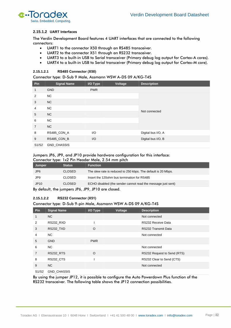
Verdin Development Board Datasheet
Toradex AG l Ebenaustrasse 10 l 6048 Horw l Switzerland l +41 41 500 48 00 l www.toradex.com l [email protected] Page | 42
2.15.1.2 UART Interfaces
The Verdin Development Board features 4 UART interfaces that are connected to the following
connectors:
• UART1 to the connector X50 through an RS485 transceiver.
• UART2 to the connector X51 through an RS232 transceiver.
• UART3 to a built-in USB to Serial transceiver (Primary debug log output for Cortex-A cores).
• UART4 to a built-in USB to Serial transceiver (Primary debug log output for Cortex-M core).
2.15.1.2.1 RS485 Connector (X50)
Connector type: D-Sub 9 Male, Assmann WSW A-DS 09 A/KG-T4S
Pin Signal Name I/O Type Voltage Description
1 GND PWR
2 NC
Not connected
3 NC
4 NC
5 NC
6 NC
7 NC
8 RS485_CON_A I/O Digital bus I/O, A
9 RS485_CON_B I/O Digital bus I/O, B
S1/S2 GND_CHASSIS
Jumpers JP6, JP9, and JP10 provide hardware configuration for this interface:
Connector type: 1x2 Pin Header Male, 2.54 mm pitch
Jumper Status Function
JP6 CLOSED The slew rate is reduced to 250 kbps. The default is 20 Mbps.
JP9 CLOSED Insert the 120ohm bus termination for RS485
JP10 CLOSED ECHO disabled (the sender cannot read the message just sent)
By default, the jumpers JP6, JP9, JP10 are closed.
2.15.1.2.2 RS232 Connector (X51)
Connector type: D-Sub 9-pin Male, Assmann WSW A-DS 09 A/KG-T4S
Pin Signal Name I/O Type Voltage Description
1 NC Not connected
2 RS232_RXD I RS232 Receive Data
3 RS232_TXD O RS232 Transmit Data
4 NC Not connected
5 GND PWR
6 NC Not connected
7 RS232_RTS O RS232 Request to Send (RTS)
8 RS232_CTS I RS232 Clear to Send (CTS)
9 NC Not connected
S1/S2 GND_CHASSIS
By using the jumper JP12, it is possible to configure the Auto Powerdown Plus function of the
RS232 transceiver. The following table shows the JP12 connection possibilities.
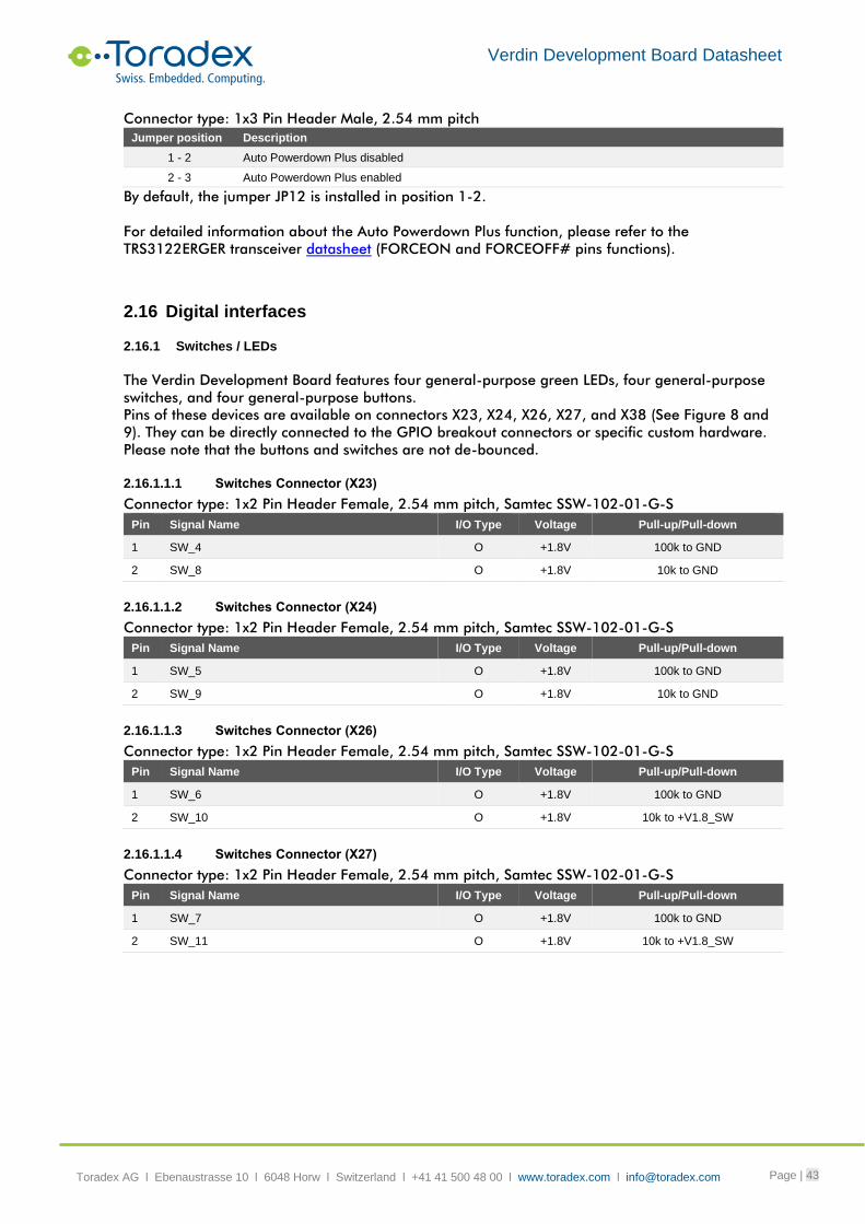
Verdin Development Board Datasheet
Toradex AG l Ebenaustrasse 10 l 6048 Horw l Switzerland l +41 41 500 48 00 l www.toradex.com l [email protected] Page | 43
Connector type: 1x3 Pin Header Male, 2.54 mm pitch
Jumper position Description
1 - 2 Auto Powerdown Plus disabled
2 - 3 Auto Powerdown Plus enabled
By default, the jumper JP12 is installed in position 1-2.
For detailed information about the Auto Powerdown Plus function, please refer to the
TRS3122ERGER transceiver datasheet (FORCEON and FORCEOFF# pins functions).
2.16 Digital interfaces
2.16.1 Switches / LEDs
The Verdin Development Board features four general-purpose green LEDs, four general-purpose
switches, and four general-purpose buttons.
Pins of these devices are available on connectors X23, X24, X26, X27, and X38 (See Figure 8 and
9). They can be directly connected to the GPIO breakout connectors or specific custom hardware.
Please note that the buttons and switches are not de-bounced.
2.16.1.1.1 Switches Connector (X23)
Connector type: 1x2 Pin Header Female, 2.54 mm pitch, Samtec SSW-102-01-G-S
Pin Signal Name I/O Type Voltage Pull-up/Pull-down
1 SW_4 O +1.8V 100k to GND
2 SW_8 O +1.8V 10k to GND
2.16.1.1.2 Switches Connector (X24)
Connector type: 1x2 Pin Header Female, 2.54 mm pitch, Samtec SSW-102-01-G-S
Pin Signal Name I/O Type Voltage Pull-up/Pull-down
1 SW_5 O +1.8V 100k to GND
2 SW_9 O +1.8V 10k to GND
2.16.1.1.3 Switches Connector (X26)
Connector type: 1x2 Pin Header Female, 2.54 mm pitch, Samtec SSW-102-01-G-S
Pin Signal Name I/O Type Voltage Pull-up/Pull-down
1 SW_6 O +1.8V 100k to GND
2 SW_10 O +1.8V 10k to +V1.8_SW
2.16.1.1.4 Switches Connector (X27)
Connector type: 1x2 Pin Header Female, 2.54 mm pitch, Samtec SSW-102-01-G-S
Pin Signal Name I/O Type Voltage Pull-up/Pull-down
1 SW_7 O +1.8V 100k to GND
2 SW_11 O +1.8V 10k to +V1.8_SW
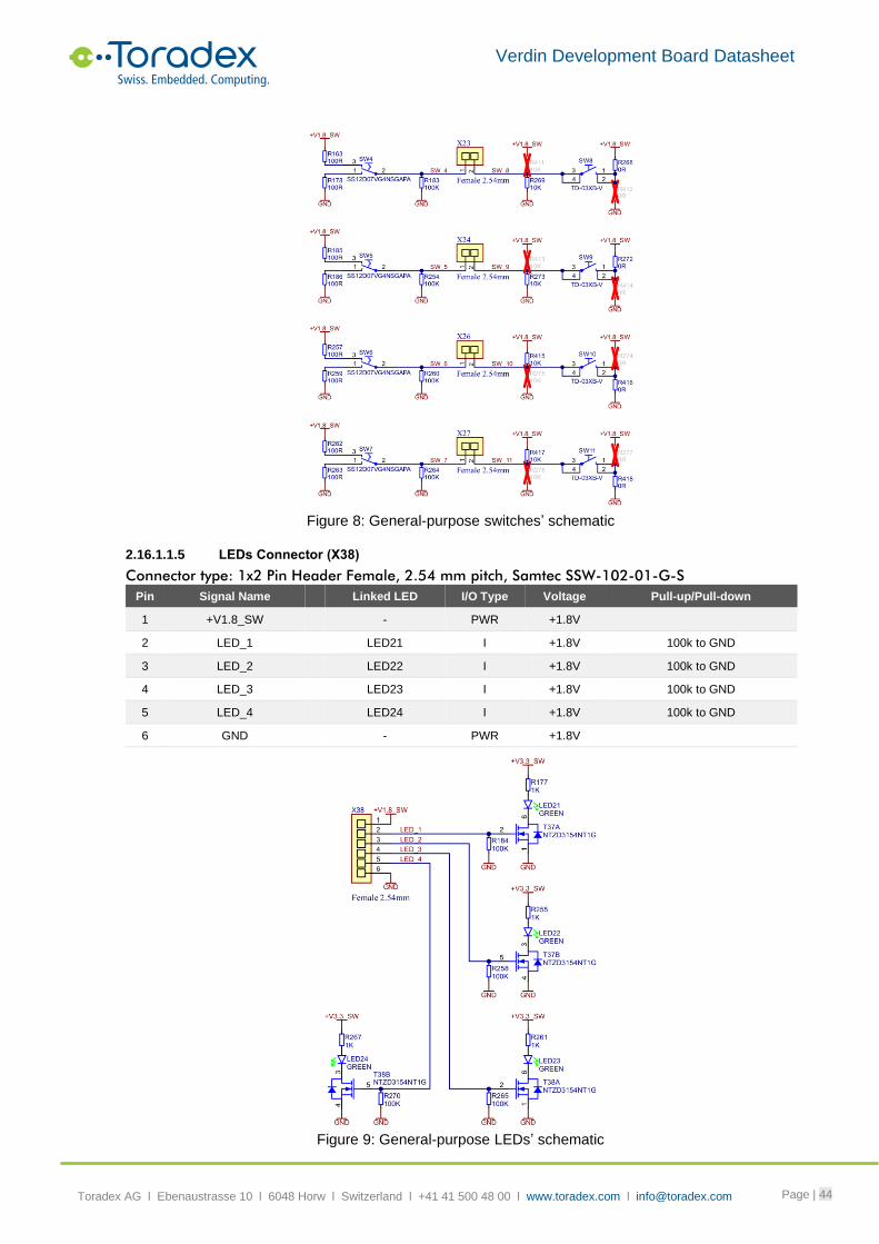
Verdin Development Board Datasheet
Toradex AG l Ebenaustrasse 10 l 6048 Horw l Switzerland l +41 41 500 48 00 l www.toradex.com l [email protected] Page | 44
Figure 8: General-purpose switches’ schematic
2.16.1.1.5 LEDs Connector (X38)
Connector type: 1x2 Pin Header Female, 2.54 mm pitch, Samtec SSW-102-01-G-S
Pin Signal Name Linked LED I/O Type Voltage Pull-up/Pull-down
1 +V1.8_SW - PWR +1.8V
2 LED_1 LED21 I +1.8V 100k to GND
3 LED_2 LED22 I +1.8V 100k to GND
4 LED_3 LED23 I +1.8V 100k to GND
5 LED_4 LED24 I +1.8V 100k to GND
6 GND - PWR +1.8V
Figure 9: General-purpose LEDs’ schematic

Verdin Development Board Datasheet
Toradex AG l Ebenaustrasse 10 l 6048 Horw l Switzerland l +41 41 500 48 00 l www.toradex.com l [email protected] Page | 45
2.16.2 Level shifters
Two level-shifters with push-pull outputs (IC31, IC 32) and one with open-drain outputs (IC33)
have been placed on the Verdin Development Board. The I/O pins of these level shifters are
connected to female pin headers X39, X40. These general-purpose level shifters can be used to
connect external 3.3V compatible hardware with the jumper wires.
2.16.2.1.1 Level Shifter Connector (X39)
Connector type: 1x10 Pin Header Female, 2.54 mm pitch
Pin Signal Name I/O Type Voltage Pull-up/Pull-down Description
1 LS_1.8V_GPIO_1 I +1.8V 100k to GND
General-purpose 1.8V level-shifted inputs
2 LS_1.8V_GPIO_2 I +1.8V 100k to GND
3 LS_1.8V_GPIO_3 I +1.8V 100k to GND
4 LS_1.8V_GPIO_4 I +1.8V 100k to GND
5 LS_1.8V_GPIO_5 O +1.8V
General-purpose 1.8V level-shifted outputs
6 LS_1.8V_GPIO_6 O +1.8V
7 LS_1.8V_GPIO_7 O +1.8V
8 LS_1.8V_GPIO_8 O +1.8V
9 LS_1.8V_SCL I/O (OD) +1.8V 10k to +V1.8_SW General-purpose 1.8V level-shifted bidirectional Inputs/Outputs with an Open Drain (OD) configuration 10 LS_1.8V_SDA I/O (OD) +1.8V 10k to +V1.8_SW
2.16.2.1.2 Level Shifter Connector (X40)
Connector type: 1x10 Pin Header Female, 2.54 mm pitch
Pin Signal Name I/O Type Voltage Pull-up/Pull-down Description
1 LS_3.3V_GPIO_1 O +3.3V
General-purpose 3.3V level-shifted outputs
2 LS_3.3V_GPIO_2 O +3.3V
3 LS_3.3V_GPIO_3 O +3.3V
4 LS_3.3V_GPIO_4 O +3.3V
5 LS_3.3V_GPIO_5 I +3.3V 100k to GND
General-purpose 3.3V level-shifted inputs
6 LS_3.3V_GPIO_6 I +3.3V 100k to GND
7 LS_3.3V_GPIO_7 I +3.3V 100k to GND
8 LS_3.3V_GPIO_8 I +3.3V 100k to GND
9 LS_3.3V_SCL I/O (OD) +3.3V 10k to +V3.3_SW General-purpose 3.3V level-shifted bidirectional Inputs/Outputs with an Open Drain (OD) configuration 10 LS_3.3V_SDA I/O (OD) +3.3V 10k to +V3.3_SW
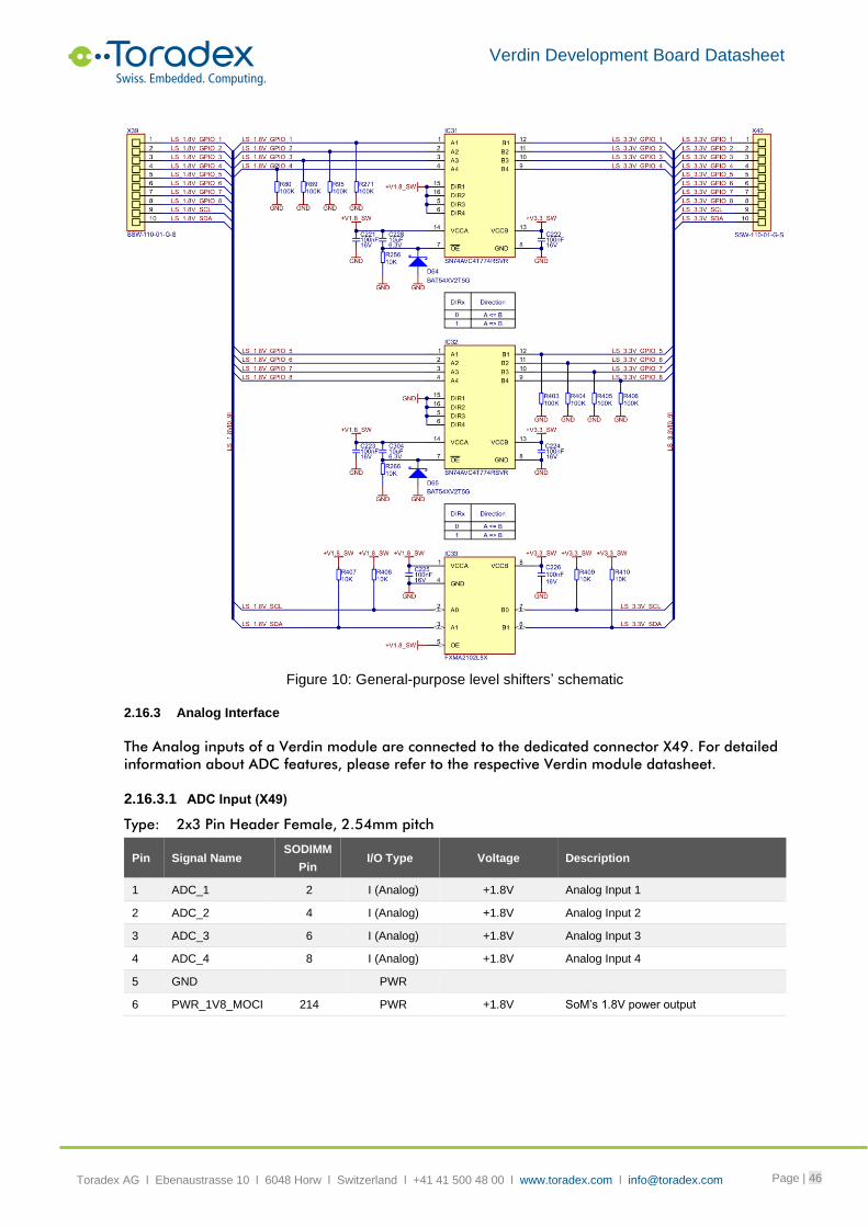
Verdin Development Board Datasheet
Toradex AG l Ebenaustrasse 10 l 6048 Horw l Switzerland l +41 41 500 48 00 l www.toradex.com l [email protected] Page | 46
Figure 10: General-purpose level shifters’ schematic
2.16.3 Analog Interface
The Analog inputs of a Verdin module are connected to the dedicated connector X49. For detailed
information about ADC features, please refer to the respective Verdin module datasheet.
2.16.3.1 ADC Input (X49)
Type: 2x3 Pin Header Female, 2.54mm pitch
Pin Signal Name SODIMM
Pin I/O Type Voltage Description
1 ADC_1 2 I (Analog) +1.8V Analog Input 1
2 ADC_2 4 I (Analog) +1.8V Analog Input 2
3 ADC_3 6 I (Analog) +1.8V Analog Input 3
4 ADC_4 8 I (Analog) +1.8V Analog Input 4
5 GND PWR
6 PWR_1V8_MOCI 214 PWR +1.8V SoM’s 1.8V power output
Verdin Development Board Datasheet
Toradex AG l Ebenaustrasse 10 l 6048 Horw l Switzerland l +41 41 500 48 00 l www.toradex.com l [email protected] Page | 47
2.17 Backup battery
A backup battery holder (BAT1) is available on the Verdin Development Board to provide backup
power to the RTC of a Verdin module when the main power is turned off.
Jumper (JP8) is used to connect or disconnect the backup battery.
Connector type: 1x2 Pin Header Male, 2.54 mm pitch
Jumper Status Function
JP8 CLOSED Battery backup voltage, connected to the Verdin module internal RTC.
JP8 OPEN Battery backup voltage disconnected from the Verdin module internal RTC.
By default, jumper JP8 is closed.
For more details on how the backup voltage is used, please refer to the respective Verdin
computer-on-module datasheet.
2.17.1 Battery Holder (BAT1)
A 20 mm (diameter) coin cell/battery should be used with the Battery Holder (BAT1). A coin-cell
battery can be used to provide power backup to the Verdin module RTC circuit when an external
power supply is not available.
Supported batteries: CR2032 or compatible coin-cell batteries.
Connector type: Renata HU2032-LF
Pin Description Voltage
1 +V_BAT +3.0V
2 GND
2.18 JTAG
The Verdin Development Board provides a JTAG interface to the JTAG port available on Verdin
modules. Connector X56 provides an interface to an external JTAG device via a Cortex Debug
Connector, which is a 10-pin 1.27mm header. The Verdin Development Board also has an on-board
JTAG debugger feature. Please check the USB Debugger section of this datasheet and the Verdin
Development Board schematic file for detailed information. This document is available on the
Toradex developer website, on the Development Board Design page.
2.18.1 JTAG Connector (X56)
Connector Type: 2x5 Pin Shrouded Header Male, 1.27mm, Samtec FTSH-105-01-L-DV-K
Pin Signal Name SODIMM
Pin I/O Type Voltage Pull-up/Pull-down Description
1 JTAG_1_VREF 7 PWR +1.8V 1.8V reference output for JTAG adapter
2 JTAG_1_TMS 13 I +1.8V Test Mode Select
3 GND PWR
4 JTAG_1_TCK 9 I +1.8V Pull-down on SOM Test Clock
5 GND PWR
6 JTAG_1_TDO 5 O +1.8V Test Data Out
WARNING!
If an external JTAG debugger is used with a Verdin Development Board, jumpers X67A – X67F should be removed. Simultaneous use of the on-board and external JTAG Debugger is not allowed. Violating this requirement may damage the Debuggers or the Verdin Development Board.

Verdin Development Board Datasheet
Toradex AG l Ebenaustrasse 10 l 6048 Horw l Switzerland l +41 41 500 48 00 l www.toradex.com l [email protected] Page | 48
7 NC Not Connected
8 JTAG_1_TDI 1 I +1.8V Test Data In
9 NC Not Connected
10 JTAG_1_TRST# 3 I (OD) +1.8V Test Reset
2.19 USB Debugger
The Verdin Development Board provides an on-board Universal USB Debugger (IC41). The
debugger is based on the FT4232HL chip and provides the following features:
• 2x UART ports connected to Verdin Module Cortex-A and Cortex-M core debug outputs
• JTAG Debugger/Programmer
• 4x GPIO used for performing basic Development Board control features: Power ON/OFF,
Reset etc.
Simplified USB Debugger architecture is shown below.
JTAG
Connector
X56
JUM PER
JP30
US B-C
Connector
X66
US B to Seria l
Conv erter IC41
FT 4232HL
JTAG (1. 8V)
UA RT (3.3V)
JTAG (3. 3V)
4x G PI O (3.3V)
US B (2. 0)
Ve
rdin
Ed
ge C
on
ne
cto
r(D
D4
SO
DIM
M)
Po
rt A
JTAG (1. 8V)
JUM PERS
X67
JUM PERS
X16
UA RT (1.8V) UA RT (1.8V) Cortex -M Debug
JTAG (1. 8V)
UA RT (3.3V)
JUM PERS
X16
UA RT (1.8V) UA RT (1.8V) Cortex -A D ebug
JUM PERS
X6
4x G PI O (1.8V) DBG _CT RL (To board c ontrol corcuit)
GP
IO C
TR
L
Po
rt B
Po
rt C
Po
rt D
Figure 11: USB Debugger architecture
The pin assignments of the FT4232HL are shown in the table below.
Pin Pin Name
I/O Type Interface Connected/Controlled Net Description
21 ADBUS4 O
GPIO
CTRL_FORCE_OFF_MOCI# Verdin Development Board FORCE OFF
22 ADBUS5 O CTRL_RESET_MICO# Verdin Module RESET
23 ADBUS6 O PWR_BTN# Verdin Development Board POWER ON/OFF
24 ADBUS7 O CTRL_RECOVERY_MICO# Verdin Module RECOVERY mode
26 BDBUS0 O
JTAG
JTAG_TCK JTAG Test Mode Select
27 BDBUS1 O JTAG_TDI JTAG Test Data Input
28 BDBUS2 I JTAG_TDO JTAG Test Data Output
29 BDBUS3 O JTAG_TMS JTAG Test Mode Set
30 BDBUS4 O JTAG_TRST# JTAG Test Mode Reset
34 BDBUS7 O JTAG_LED JTAG activity LED
38 CDBUS0 O UART
UART_4_RXD Receiver Data of Cortex-M debug UART
39 CDBUS1 I UART_4_TXD Transmitter Data of Cortex-M debug UART
48 DDBUS0 O UART
UART_3_RXD Receiver Data of Cortex-A debug UART
52 DDBUS1 I UART_3_TXD Transmitter Data of Cortex-A debug UART
Verdin Development Board Datasheet
Toradex AG l Ebenaustrasse 10 l 6048 Horw l Switzerland l +41 41 500 48 00 l www.toradex.com l [email protected] Page | 49
The debug interface is accessible via the separate USB-C connector X66.
2.19.1.1 USB Debugger Connector (X66)
Connector type: USB-C, Amphenol 12401598E4#2A
Pin Signal Name I/O Type Voltage Pull-up/Pull-down Description
A1 GND PWR
A2 NC Not Connected
A3 NC
A4 +V5_DBG PWR +5V FTDI debugger power supply input
A5 USB_DBG_CC1 5.1k to GND Type-C configuration channel signal 1
A6 USB_DBG_CON_P I/O Positive Differential USB 2.0 Signal
A7 USB_DBG_CON_N I/O Negative Differential USB 2.0 Signal
A8 NC Not Connected
A9 +V5_DBG PWR +5V FTDI debugger power supply input
A10 NC Not Connected
A11 NC
A12 GND PWR
B1 GND PWR
B2 NC Not Connected
B3 NC
B4 +V5_DBG PWR +5V FTDI debugger power supply input
B5 USB_DBG_CC2 5.1k to GND Type-C configuration channel signal 2
B6 USB_DBG_CON_P I/O Positive Differential USB 2.0 Signal
B7 USB_DBG_CON_N I/O Negative Differential USB 2.0 Signal
B8 NC Not Connected
B9 +V5_DBG PWR +5V FTDI debugger power supply input
B10 NC Not Connected
B11 NC
B12 GND PWR
SH1/SH2 GND_CHASSIS
SH3/SH4 GND_CHASSIS
The FTDI JTAG interface is connected to the SoM and the Verdin Development Board via the X67
jumper area.
2.19.1.1.1 Jumper Area (X67)
Connector type: 2x6 Pin Header Male, 2.54 mm pitch
Signal Name I/O Type Pin Pin I/O Type Signal Name Voltage
FTDI_JTAG_TCK O B1 A1 I JTAG_1_TCK +1.8V
FTDI_JTAG_TDI O B2 A2 I JTAG_1_TDI +1.8V
FTDI_JTAG_TDO I B3 A3 O JTAG_1_TDO +1.8V
FTDI_JTAG_TMS O B4 A4 I JTAG_1_TMS +1.8V
FTDI_JTAG_TRST# O B5 A5 I JTAG_1_TRST# +1.8V
FTDI_JTAG_VREF PWR B6 A6 PWR JTAG_1_VREF +1.8V

Verdin Development Board Datasheet
Toradex AG l Ebenaustrasse 10 l 6048 Horw l Switzerland l +41 41 500 48 00 l www.toradex.com l [email protected] Page | 50
By changing the configuration of the jumpers X67A-X67F, the user can connect or disconnect the
on-board JTAG Debugger to/from the SoM.
Connector type: 2x6 Pin Header Male, 2.54 mm pitch
Jumper Status Function
X67A, X67B, X67C, X67D, X67E, X67F
CLOSED FTDI JTAG.Debugger connected to SoM
X67A, X67B, X67C, X67D, X67E, X67F
OPEN FTDI JTAG.Debugger disconnected from SoM
By default, jumpers X67A, X67B, X67C, X67D, X67E, X67F are closed.
The FTDI GPIO pins are connected via the X6 pin header. For details, please refer to the X6 pinout.
The FTDI GPIO pins can be used to control the Development Board or as regular GPIO (outputs
only) to control other parts of the board
Jumper JP30 should be configured according to the desired FTDI GPIO pins functionality. Possible
configurations are listed in the table below.
Type: 1x3 Pin Header Male, 2.54 mm pitch
Jumper position Description
1-2 FTDI GPIO pins can be used to control Verdin Development Board modes.
2-3 FTDI GPIO pins can be used as regular GPIO (outputs only)
By default, jumper JP30 is installed in position 1-2.
2.20 Low-speed IO pins configuration
The Low-speed IO pins’ breakout connectors offer the flexibility to map the IO pins of the Verdin
module to either the on-board function or to external hardware.
The factory setting is a straight-through jumper setting, meaning that the X3-A row is connected
straight to the X3-B row. This is also true for the connectors X6 and X16.
All signals residing on the male header are also available on a female connector in parallel to
allow easy measurement, probing, and re-routing.
To map the SODIMM pin with the corresponding SoC ball name, which is specific to individual
Verdin modules, please refer to the applicable Verdin module datasheet.
WARNING!
If an external JTAG debugger is used with a Verdin Development Board, jumpers X67A – X67F should be removed. Simultaneous use of the on-board and external JTAG Debugger is not allowed. Violating this requirement may damage the debugger or the Verdin Development Board.

Verdin Development Board Datasheet
Toradex AG l Ebenaustrasse 10 l 6048 Horw l Switzerland l +41 41 500 48 00 l www.toradex.com l [email protected] Page | 51
2.20.1 Low-speed IO pins 1 Male (X3 Row A and B)
Connector Type: 2x30Pin Male, 2.54mm
SoM Side Peripheral Side I/O Type Voltage Pull-up/Pull-down Description
SODIMM Pin Signal Name Pin Pin Signal Name
12 SODIMM_12 A1 B1 I2C_1_SDA I/O +1.8V 1.8k to +V1.8_SW Generic I2C Data
14 SODIMM_14 A2 B2 I2C_1_SCL O +1.8V 1.8k to +V1.8_SW Generic I2C Clock
15 SODIMM_15 A3 B3 PWM_1 O +1.8V General-purpose PWM
16 SODIMM_16 A4 B4 PWM_2 O +1.8V
20 SODIMM_20 A5 B5 CAN_1_TX O +1.8V 10k to +V1.8_SW CAN port 1 transmit pin
22 SODIMM_22 A6 B6 CAN_1_RX I +1.8V CAN port 1 receive pin
24 SODIMM_24 A7 B7 CAN_2_TX O +1.8V 10k to +V1.8_SW CAN port 2 transmit pin
26 SODIMM_26 A8 B8 CAN_2_RX I +1.8V CAN port 2 receive pin
GND A9 B9 GND PWR
+V1.8_SW A10 B10 +V1.8_SW PWR +1.8V +1.8V power supply output
30 SODIMM_30 A11 B11 I2S_1_BCLK O +1.8V I2S Serial Clock (Transmit Bit Clock)
32 SODIMM_32 A12 B12 I2S_1_SYNC O +1.8V I2S Field Select (Transmit Frame Sync)
34 SODIMM_34 A13 B13 I2S_1_D_OUT O +1.8V I2S Data Output
36 SODIMM_36 A14 B14 I2S_1_D_IN I +1.8V I2S Data Input
38 SODIMM_38 A15 B15 I2S_1_MCLK O +1.8V I2S Master clock output
GND A16 B16 GND PWR
42 SODIMM_42 A17 B17 I2S_2_BCLK O +1.8V I2S Serial Clock (Transmit Bit Clock)
44 SODIMM_44 A18 B18 I2S_2_SYNC O +1.8V I2S Field Select (Transmit Frame Sync)
46 SODIMM_46 A19 B19 I2S_2_D_OUT O +1.8V I2S Data Output
48 SODIMM_48 A20 B20 I2S_2_D_IN I +1.8V I2S Data Input
52 SODIMM_52 A21 B21 QSPI_1_CLK O +1.8V QSPI Serial Clock
54 SODIMM_54 A22 B22 QSPI_1_CS# O +1.8V QSPI Chip Select 0
56 SODIMM_56 A23 B23 QSPI_1_IO0 I/O +1.8V QSPI Serial I/Os for command, address, and data 58 SODIMM_58 A24 B24 QSPI_1_IO1 I/O +1.8V
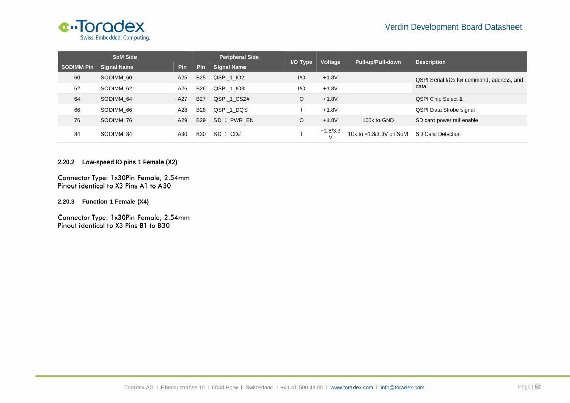
Verdin Development Board Datasheet
Toradex AG l Ebenaustrasse 10 l 6048 Horw l Switzerland l +41 41 500 48 00 l www.toradex.com l [email protected] Page | 52
SoM Side Peripheral Side I/O Type Voltage Pull-up/Pull-down Description
SODIMM Pin Signal Name Pin Pin Signal Name
60 SODIMM_60 A25 B25 QSPI_1_IO2 I/O +1.8V QSPI Serial I/Os for command, address, and data 62 SODIMM_62 A26 B26 QSPI_1_IO3 I/O +1.8V
64 SODIMM_64 A27 B27 QSPI_1_CS2# O +1.8V QSPI Chip Select 1
66 SODIMM_66 A28 B28 QSPI_1_DQS I +1.8V QSPI Data Strobe signal
76 SODIMM_76 A29 B29 SD_1_PWR_EN O +1.8V 100k to GND SD card power rail enable
84 SODIMM_84 A30 B30 SD_1_CD# I +1.8/3.3
V 10k to +1.8/3.3V on SoM SD Card Detection
2.20.2 Low-speed IO pins 1 Female (X2)
Connector Type: 1x30Pin Female, 2.54mm
Pinout identical to X3 Pins A1 to A30
2.20.3 Function 1 Female (X4)
Connector Type: 1x30Pin Female, 2.54mm
Pinout identical to X3 Pins B1 to B30
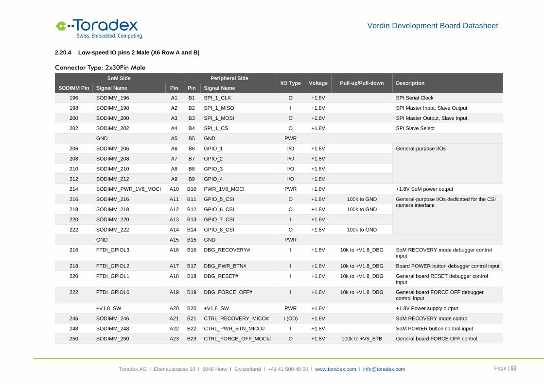
Verdin Development Board Datasheet
Toradex AG l Ebenaustrasse 10 l 6048 Horw l Switzerland l +41 41 500 48 00 l www.toradex.com l [email protected] Page | 53
2.20.4 Low-speed IO pins 2 Male (X6 Row A and B)
Connector Type: 2x30Pin Male
SoM Side Peripheral Side I/O Type Voltage Pull-up/Pull-down Description
SODIMM Pin Signal Name Pin Pin Signal Name
196 SODIMM_196 A1 B1 SPI_1_CLK O +1.8V SPI Serial Clock
198 SODIMM_198 A2 B2 SPI_1_MISO I +1.8V SPI Master Input, Slave Output
200 SODIMM_200 A3 B3 SPI_1_MOSI O +1.8V SPI Master Output, Slave Input
202 SODIMM_202 A4 B4 SPI_1_CS O +1.8V SPI Slave Select
GND A5 B5 GND PWR
206 SODIMM_206 A6 B6 GPIO_1 I/O +1.8V General-purpose I/Os
208 SODIMM_208 A7 B7 GPIO_2 I/O +1.8V
210 SODIMM_210 A8 B8 GPIO_3 I/O +1.8V
212 SODIMM_212 A9 B9 GPIO_4 I/O +1.8V
214 SODIMM_PWR_1V8_MOCI A10 B10 PWR_1V8_MOCI PWR +1.8V +1.8V SoM power output
216 SODIMM_216 A11 B11 GPIO_5_CSI O +1.8V 100k to GND General-purpose I/Os dedicated for the CSI camera interface
218 SODIMM_218 A12 B12 GPIO_6_CSI O +1.8V 100k to GND
220 SODIMM_220 A13 B13 GPIO_7_CSI I +1.8V
222 SODIMM_222 A14 B14 GPIO_8_CSI O +1.8V 100k to GND
GND A15 B15 GND PWR
216 FTDI_GPIOL3 A16 B16 DBG_RECOVERY# I +1.8V 10k to +V1.8_DBG SoM RECOVERY mode debugger control input
218 FTDI_GPIOL2 A17 B17 DBG_PWR_BTN# I +1.8V 10k to +V1.8_DBG Board POWER button debugger control input
220 FTDI_GPIOL1 A18 B18 DBG_RESET# I +1.8V 10k to +V1.8_DBG General board RESET debugger control input
222 FTDI_GPIOL0 A19 B19 DBG_FORCE_OFF# I +1.8V 10k to +V1.8_DBG General board FORCE OFF debugger control input
+V1.8_SW A20 B20 +V1.8_SW PWR +1.8V +1.8V Power supply output
246 SODIMM_246 A21 B21 CTRL_RECOVERY_MICO# I (OD) +1.8V SoM RECOVERY mode control
248 SODIMM_248 A22 B22 CTRL_PWR_BTN_MICO# I +1.8V SoM POWER button control input
250 SODIMM_250 A23 B23 CTRL_FORCE_OFF_MOCI# O +1.8V 100k to +V5_STB General board FORCE OFF control

Verdin Development Board Datasheet
Toradex AG l Ebenaustrasse 10 l 6048 Horw l Switzerland l +41 41 500 48 00 l www.toradex.com l [email protected] Page | 54
SoM Side Peripheral Side I/O Type Voltage Pull-up/Pull-down Description
SODIMM Pin Signal Name Pin Pin Signal Name
252 SODIMM_252 A24 B24 CTRL_WAKE1_MICO# I +1.8V 5.1k to +V1.8_SW WAKE signal to out SoM from SLEEP mode
254 SODIMM_254 A25 B25 CTRL_PWR_EN_MOCI O +1.8V 100k to GND Power enable for the on-board peripherals
256 SODIMM_256 A26 B26 CTRL_SLEEP_MOCI# O +1.8V Sleep signal for the on-board peripherals
258 SODIMM_258 A27 B27 CTRL_RESET_MOCI# O +3.3V 10k to +V3.3_SW Reset for the on-board peripherals
260 SODIMM_260 A28 B28 CTRL_RESET_MICO# I (OD) +1.8V SoM’s RESET signal
GND A29 B29 GND PWR
196 +V1.8_SW A30 B30 +V1.8_SW PWR +1.8V +1.8V Power supply output
2.20.5 Function 2 Female (X5)
Connector Type: 1x30Pin Female, 2.54mm
Pinout identical to X6 Pins A1 to A30
2.20.6 Low-speed IO pins 2 Female (X7)
Connector Type: 1x30Pin Female, 2.54mm
Pinout identical to X6 Pins B1 to B30
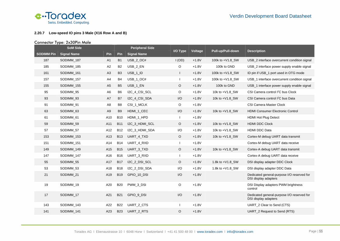
Verdin Development Board Datasheet
Toradex AG l Ebenaustrasse 10 l 6048 Horw l Switzerland l +41 41 500 48 00 l www.toradex.com l [email protected] Page | 55
2.20.7 Low-speed IO pins 3 Male (X16 Row A and B)
Connector Type: 2x30Pin Male
SoM Side Peripheral Side I/O Type Voltage Pull-up/Pull-down Description
SODIMM Pin Signal Name Pin Pin Signal Name
187 SODIMM_187 A1 B1 USB_2_OC# I (OD) +1.8V 100k to +V1.8_SW USB_2 interface overcurrent condition signal
185 SODIMM_185 A2 B2 USB_2_EN O +1.8V 100k to GND USB_2 interface power supply enable signal
161 SODIMM_161 A3 B3 USB_1_ID I +1.8V 100k to +V1.8_SW ID pin if USB_1 port used in OTG mode
157 SODIMM_157 A4 B4 USB_1_OC# I +1.8V 100k to +V1.8_SW USB_1 interface overcurrent condition signal
155 SODIMM_155 A5 B5 USB_1_EN O +1.8V 100k to GND USB_1 interface power supply enable signal
95 SODIMM_95 A6 B6 I2C_4_CSI_SCL O +1.8V 10k to +V1.8_SW CSI Camera control I2C bus Clock
93 SODIMM_93 A7 B7 I2C_4_CSI_SDA I/O +1.8V 10k to +V1.8_SW CSI Camera control I2C bus Data
91 SODIMM_91 A8 B8 CSI_1_MCLK O +1.8V CSI Camera Master Clock
63 SODIMM_63 A9 B9 HDMI_1_CEC I/O +1.8V 10k to +V1.8_SW HDMI Consumer Electronic Control
61 SODIMM_61 A10 B10 HDMI_1_HPD I +1.8V HDMI Hot Plug Detect
59 SODIMM_59 A11 B11 I2C_3_HDMI_SCL O +1.8V 10k to +V1.8_SW HDMI DDC Clock
57 SODIMM_57 A12 B12 I2C_3_HDMI_SDA I/O +1.8V 10k to +V1.8_SW HDMI DDC Data
153 SODIMM_153 A13 B13 UART_4_TXD O +1.8V 10k to +V1.8_SW Cortex-M debug UART data transmit
151 SODIMM_151 A14 B14 UART_4_RXD I +1.8V Cortex-M debug UART data receive
149 SODIMM_149 A15 B15 UART_3_TXD O +1.8V 10k to +V1.8_SW Cortex-A debug UART data transmit
147 SODIMM_147 A16 B16 UART_3_RXD I +1.8V Cortex-A debug UART data receive
55 SODIMM_55 A17 B17 I2C_2_DSI_SCL O +1.8V 1.8k to +V1.8_SW DSI display adapter DDC Clock
53 SODIMM_53 A18 B18 I2C_2_DSI_SDA I/O +1.8V 1.8k to +V1.8_SW DSI display adapter DDC Data
21 SODIMM_21 A19 B19 GPIO_10_DSI I/O +1.8V Dedicated general-purpose I/O reserved for DSI display adapters
19 SODIMM_19 A20 B20 PWM_3_DSI O +1.8V DSI Display adapters PWM brightness control
17 SODIMM_17 A21 B21 GPIO_9_DSI I/O +1.8V Dedicated general-purpose I/O reserved for DSI display adapters
143 SODIMM_143 A22 B22 UART_2_CTS I +1.8V UART_2 Clear to Send (CTS)
141 SODIMM_141 A23 B23 UART_2_RTS O +1.8V UART_2 Request to Send (RTS)

Verdin Development Board Datasheet
Toradex AG l Ebenaustrasse 10 l 6048 Horw l Switzerland l +41 41 500 48 00 l www.toradex.com l [email protected] Page | 56
SoM Side Peripheral Side I/O Type Voltage Pull-up/Pull-down Description
SODIMM Pin Signal Name Pin Pin Signal Name
139 SODIMM_139 A24 B24 UART_2_TXD O +1.8V UART_2 Transmit Data
137 SODIMM_137 A25 B25 UART_2_RXD I +1.8V UART_2 Receive Data
135 SODIMM_135 A26 B26 UART_1_CTS I +1.8V UART_1 Clear to Send (CTS)
133 SODIMM_133 A27 B27 UART_1_RTS O +1.8V 10k to +V1.8_SW UART_1 Request to Send (RTS)
131 SODIMM_131 A28 B28 UART_1_TXD O +1.8V UART_1 Transmit Data
129 SODIMM_129 A29 B29 UART_1_RXD I +1.8V UART_1 Receive Data
GND A30 B30 GND PWR
2.20.8 Low-speed IO pins 3 Female (X15)
Connector Type: 1x30 Pin Female, 2.54mm
Pinout identical to X16 Pins A1 to A30
2.20.9 Function 3 Female (X17)
Connector Type:1x30 Pin Female, 2.54mm
Pinout identical to X16 Pins B1 to B30
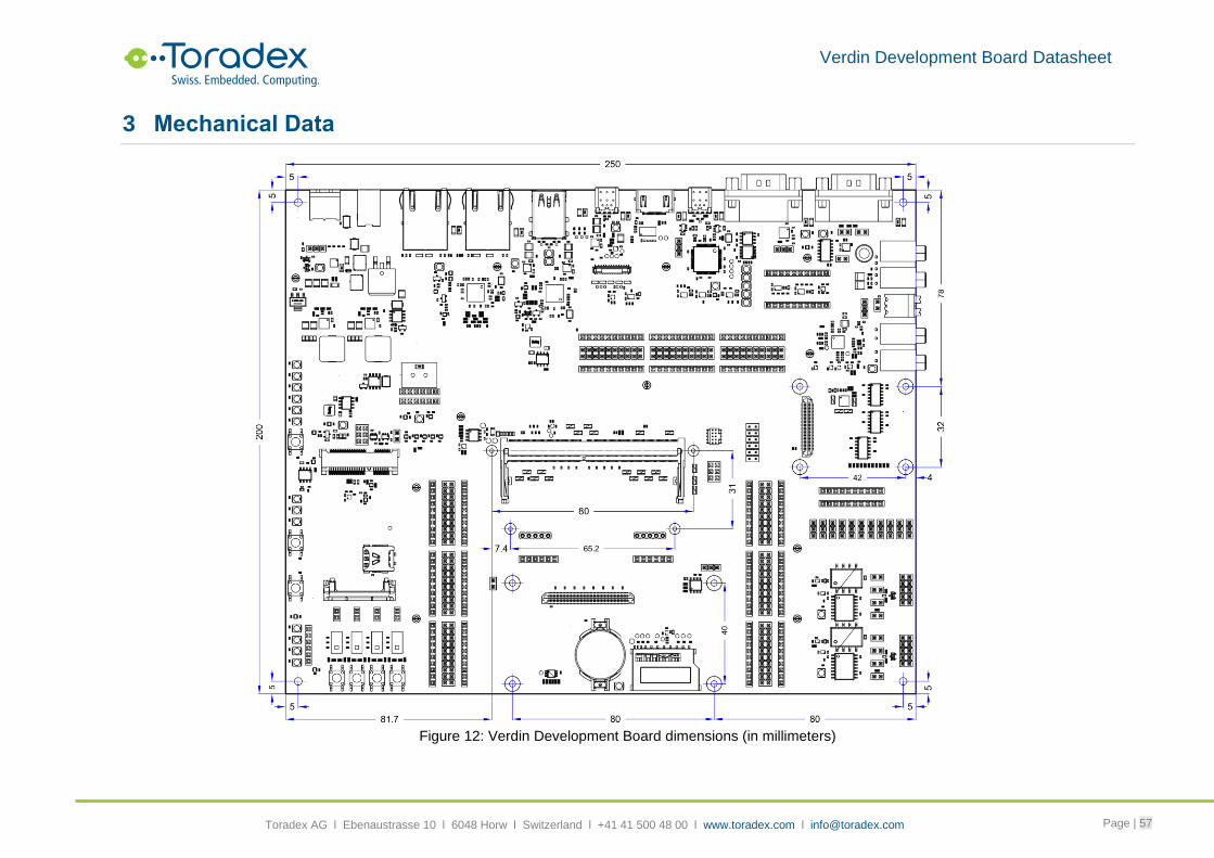
Verdin Development Board Datasheet
Toradex AG l Ebenaustrasse 10 l 6048 Horw l Switzerland l +41 41 500 48 00 l www.toradex.com l [email protected] Page | 57
3 Mechanical Data
Figure 12: Verdin Development Board dimensions (in millimeters)

Verdin Development Board Datasheet
Toradex AG l Ebenaustrasse 10 l 6048 Horw l Switzerland l +41 41 500 48 00 l www.toradex.com l [email protected] Page | 58
4 Design Data
The design data for Toradex Development Board is freely available in the Altium Designer format.
The design data includes schematics, layout, and component libraries.
To download the Development Board design data, please use the link below:
http://developer.toradex.com/carrier-board-design
5 Product Compliance
Up-to-date information about product compliance such as RoHS, CE, UL-94, Conflict Mineral,
REACH, etc. can be found on our website at http://www.toradex.com/support/product-compliance
Verdin Development Board Datasheet
Toradex AG l Ebenaustrasse 10 l 6048 Horw l Switzerland l +41 41 500 48 00 l www.toradex.com l [email protected] Page | 59
DISCLAIMER:
Copyright © Toradex AG. All rights are reserved. The information and content in this document are
provided “as-is” with no warranties of any kind and are for informational purposes only. Data and
information have been carefully checked and are believed to be accurate; however, no liability or
responsibility for any errors, omissions, or inaccuracies is assumed.
Brand and product names are trademarks or registered trademarks of their respective owners.
Specifications are subject to change without notice.