vcsel arrays expanding the range of high-power … 2015 0587-000317.pdf · vcsel arrays expanding...
TRANSCRIPT

VCSEL ARRAYS EXPANDING THE RANGE OF HIGH-POWER LASER SYSTEMS AND APPLICATIONS
Armand Pruijmboom1, Rolf Apetz1, Ralf Conrads1, Carsten Deppe1, Guenther Derra1, Stephan Gronenborn1, Xi Gu2, Johanna Sophie Kolb1, Michael Miller3, Holger Moench1, Felix Ogiewa1,
Pavel Pekarski1, Jens Pollmann-Retsch1, Ulrich Weichmann1
1 Philips GmbH Photonics Aachen, Steinbachstrasse 15, 52074 Aachen, Germany
2 Philips Electronics Netherlands, Kastanjelaan 400, 5616 LZ Eindhoven, The Netherlands 3 Philips GmbH Photonics Ulm, Lise-Meitner-Str. 13, 89081 Ulm, Germany
URL: www.philips.com/photonics, Email: [email protected]
Abstract
Thermal treatment may be by far the most frequent
process used in manufacturing, but only at a few places
lasers could make an inroad. For thermal treatment
homogeneous illumination of large areas at a lower
brightness, and accurate temporal as well as spatial
control of the power is required. This is complicated for
conventional high-power lasers, while VCSEL arrays
inherently have these capabilities.
Because of their fast switching capability and low
power dissipation, vertical-cavity surface emitting
laser-diodes (VCSELs) have been widely used for
datacom and sensing applications. By forming large-
area arrays with hundreds of VCSELs per mm2, their
use can be further expanded to high-power applications.
In this way power densities of several W/mm2 are
achieved, making VCEL arrays an ideal solution for
many heating applications, ranging from melting and
welding of plastics and laminates to curing, drying and
sintering of coatings.
A turn-key system concept has been developed allowing
fast and easy configuring systems to the specifications
of the applications. The compact and robust system can
be built directly into the manufacturing equipment, thus
making expensive fibers and homogenizing optics
superfluous. These systems are now finding their first
inroads into industrial applications and have been
designed-in into commercially available production
machines.
Introduction
For the manufacturing of numerous industrial and
consumer products, thermal processes are being used.
Traditional ways for coupling the energy for heating
into the work piece encompass burners, hot air blowers,
convection ovens, micro-waves, induction heating and
halogen lamps. All these methods have their merits and
are probably there to stay for specific applications but
in general they heat and switch slowly. Because they
heat slowly they need to be bulky for sufficient
throughput. Because they switch slowly, the dosing is
inaccurate. Furthermore, these methods often suffer
from inhomogeneous spatial dosing.
Edge-emitting laser diodes and diode-pumped solid-
state lasers have superior brightness compared to
conventional radiative heat sources, but for many
heating applications the power density is too high and
the treated area too small. By optical means this power
can be diluted to homogeneously heat larger areas, but
this requires complex optics, making such systems
bulky, vulnerable and expensive [1].
Like LEDs are nowadays replacing incandescent- and
gas-discharge lamps for general lighting purposes,
significantly increasing their efficiency and reliability,
VCSELs will provide the future lamps for heating. Both
manufacturing as well as assembly of VCSEL heat
sources have many similarities with those of LEDs,
providing cost advantages.
Without optical means they provide a very
homogeneous illumination that can in principle be
scaled to arbitrary areas. Because they can directly
illuminate the work piece they are very compact,
eliminating the need of fiber-coupled systems. Both in
time, as well as spatially, the power can be controlled
accurately and their narrow bandwidth allows tailoring
it to the absorption spectrum of the treated material. The
inherent robustness of VCSELs and use of standard
LED assembly methods provide systems with high
reliability, resistant against harsh workshop conditions
[2,3,4].
High-power VCSEL array systems
VCSEL are produced with standard semiconductor
wafer processing methods- and equipment, involving
lithography, wet- or reactive-ion etching and metal- and
dielectric deposition. Unlike edge-emitting lasers-
diodes, their manufacturing is completed after wafer
1
Invited plenary paper presented at ICALEO, Oct. 22, 2015 in Atlanta, USA

processing is finished. They can be tested and binned by
probe testing on wafer level, such that after dicing, the
good dice can be selected for the subsequent assembly
process. Assembly involves standard semiconductor
assembly processes- and equipment, for pick-and-place,
die attach and wire bonding.
Figure 1 Schematic cross section of a VCSEL
Figure 1 shows a schematic cross-section of the active
area of a single VCSEL. The active layer, consisting of
multiple quantum wells, is situated between epitaxially
grown so-called distributed Bragg reflectors,
abbreviated DBR mirrors. These mirrors consist of
AlxGa1-xAs multi-layers with alternating low and high
Al content and, hence, alternating magnitude of the
refractive index. The lower mirrors are doped n-type
and the upper mirrors p-type, which also allows to use
these mirrors as leads for the electrical current. Close to
the quantum-well region a so-called current
confinement layer is grown, which consists of an
AlxGa1-xAs layer with x ≈ 1. After etching so-called
mesas, isolating the p-doped areas from each other, this
layer is exposed and during a selective oxidation it is
transferred into an isolating Al2O3 layer, except for the
central region. The width of the isolating region is
determined by the oxidation time- and temperature and
the Al content. The cathode contact is made by a
metallic contact to the highly n-type doped substrate,
either on the backside of the wafer or the front-side and
the anode contact is provide by a ring-shaped metal
contact on top of the p-type DBR mirror. For high-
power arrays, the cathode is usually made on the
backside of the wafer by a blanket deposition and the p-
contact is enforced with a thick electroplated Au layer
for adequate distribution of the current over the array.
Depending on the mesa and aperture dimensions, the
optical output power per VCSEL amounts 1 to 10 mW.
The wave-length can be varied by tuning the resonance
frequency of the cavity and emission spectrum of the
quantum wells between 700 and 1200 nm, but for high-
efficiency, wavelengths should be restricted to the range
of 800 to 1100 nm. By packing up to 600 VCSELs per
mm2 in an array, as depicted in Figure 2, optical power
densities of several W/mm2 can be achieved.
Figure 2 Top view of VCSEL array
In the array in this figure, the VCSEL are hexagonally
packed at 40 µm pitch, such that a VCSEL array chip
with dimensions of 1.8 X 2.0 mm2, including the
bonding pad area, contains 2205 individual VCSELs. At
an output power around 4 mW per VCSEL, output
powers of 8 – 10 W per chip are obtained.
Figure 3 VCSEL array emitter containing 28 VCSEL
array chips, with each 2205 individual VCSELs
Larger arrays can be formed by assembling multiple
array chips next to each other, forming so-called
emitters. The emitter shown in Figure 3 contains 28
array chips of 1.8 X 2.0 mm2. The chips are soldered on
ceramic sub-mounts with high thermal conductance and
these sub-mounts are soldered on a NiAu plated copper
cooling structure. The 28 chips are divided in two
“zones” of 14 chips, which are contacted in series by
wire-bonding from the anode bonding pad on the chip
to the solder pad of the next chip. A board on either end
of the emitter is used for electrically connecting one
zone to the power-supply connectors. Bolts for
mechanically fixating the emitters to these connectors
and the housing also serve for electrically contacting the
boards to the connectors. The emitting area of such an
emitter is 8.5 X 41 mm, divided up in two addressable
zones of each 2.2 X 41 mm2. One emitter can deliver a
total optical output power of > 400 W.
2

Even larger arrays are formed by placing multiple
emitters next to each other. An example where 12
emitters forming a 4.8 kW module is shown in Figure 4.
Figure 4 A 4.8 kW VCSEL module containing 12
emitters with 24 individually addressable zones
Figure 5 Power supply for 12 channels of
6 VCSEL emitters
The housing is not hermetically sealed but instead an
inlet is provided for purge gas, to prevent condensation
on the water-cooled emitters. Additional purge gas
inlets are available to provide a flow parallel to the
outside of the cover window, to prevent vapours from
heating the work piece polluting this window. Per block
of 6 emitters there is a water in- and outlet on the
backside of the module and space for connecting two
power-cable plugs.
The power supply shown in Figure 5 is configured to be
able to drive up to 12 channels of one such block of 6
emitters. An EtherCAT© industrial bus interface
enables software control of the power. Within 1 ms it
can switch from zero to maximum power.
Modules of infinite length and power could be realized
in this manner but in practicality it should be limited to
about 1 m length and 50 kW optical power.
Figure 6 Optical output power and wall-plug efficiency
of an 808 nm VCSEL array emitter
The optical output power and wall-plug efficiency of an
808 nm wavelength VCSEL array emitter is shown in
Figure 6. At a current of about 9A an output power of
400 W, corresponding to 115 W/cm2, is achieved at an
electrical to optical efficiency of about 40%.
The near-field of the VCSEL emitters, as shown in
Figure 7, displays a very homogeneous illumination. At
larger distance the existing ripple is further evened out,
but at the cost of a reduction of the average power
density.
Figure 7 Near-field of VCSEL emitter at a distance of
30 mm from the VCSEL surface
0
0,1
0,2
0,3
0,4
0,5
0
100
200
300
400
500
0 2 4 6 8 10 12
Popt
WPEO
pti
calP
ow
er
(W)
Current (A)
Wal
l-P
lug
Effi
cien
cy
3

Advantages of high power VCSEL arrays
As compared to conventional heating methods, VCSEL
arrays offer a number of advantages. The power density
of >100W/cm2 allows increased process speed.
Figure 8 Schematic heat pattern for VCSEL heating vs.
a conventional belt oven
In Figure 8, it is sketched how material is flowing
through a conventional belt oven. Due to the low rate of
energy transfer, it needs to stay a long time in the oven
and therefore these ovens need to be made long enough
for sufficient throughput. In contrast, the VCSEL
system dimensions can remain a fraction of that of the
work piece, because of its high power density. The low
divergence of the VCSEL illumination, combined with
the fast switching speed, allows to heat only when and
where it is needed, which allows dimming spatially and
over time, to only heat the work piece and not its
surrounding. The narrow spectrum as compared to
halogen lamps is stable when dimming, allowing
accurate process control and can be chosen to overlap
with maxima in the absorption spectrum of the material,
to increase the overall energy efficiency of the process.
The inherent high life-time of solid state devices of
>> 10,000 hrs. offers low maintenance- and operational
costs.
Conventional edge-emitting diode-lasers are able to
provide similar advantages. However, their elliptical
beam characteristics and high power density requires
either expensive, bulky, fragile optics or scanner
systems, for diluting and homogenizing the power [1].
Because of their circular far field and homogenization
by overlapping radiation of a larger number of
individual VCSELs, VCSEL arrays offer homogeneous
illumination without optics and can be placed directly in
the vicinity of the work piece. They are robust against
back reflection, are compact and easy to integrate and
because of their simplicity a factor of 2-5 cheaper than
comparable edge-emitter diode laser systems.
The division of the emitting area in addressable zones
and fast switching within milliseconds, allows spatial
control of the heating profile, as depicted in Figure 9.
Figure 9 Spatial heating-profile control by addressable
zones
This can be used e.g. to compensate for increased heat
conduction at the edges of a work piece and can be
adjusted dynamically in case of irregular shapes or non-
linear movement of the material. When integrated with
an arrays of thermal sensors, closed-loop control of the
generated heating patterns is possible.
In roll-to-roll processes photonic curing and thermal
treatment is used on surface layers, metallization lines,
coatings and glues. Here the addressability of the
VCSEL heating systems can be used to generate
dynamic heat patterns with structured pulsed light, as
schematically depicted in Figure 10.
Figure 10 Generation of dynamic heat patterns with
structured pulsed light
VCSEL
Conventional
Current:
VCSELs:
IR power:
Target:
4
Pixilated heating systems
While the area heating systems are addressable, the
smallest dimension of the addressable zones is 2.2 X 41
mm2, due to connecting 14 chips of 1.8 X 2.0 mm2 in
series. This is sufficient for most purposes but for some
applications this is still too coarse. Using smaller chips
that are individually addressable, so-called pixelated
heating modules can be made with VCSEL arrays. As
for every channel two current leads are needed, that
need to carry several Amperes, the biggest challenge for
finer pixelation is determined by finding space for the
contacting area and the volume of the current leads. In
order to alleviate this challenge, the driver electronics
has been integrated in the module such that for every
module with 32 channels, one pair of supply cables and
a signal cable is needed, as seen in Figure 11.
Figure 11 Pixelated heating system with 32-channels
of 1.5 W output power
The emitting area of each VCSEL array is 0.5 X 0.7
mm2, delivering 1.5 W of optical power. By the use of
micro-lens arrays and secondary optics, these
dimensions can be de-magnified by a factor of up to
five, resulting in 100 X 140 µm2 pixels with a power
density of > 104 W/cm2 and a pitch of 100 µm (250 DPI)
[5,6].
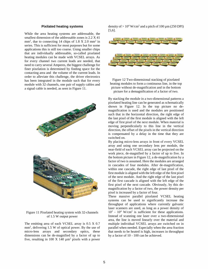
Figure 12 Two-dimensional stacking of pixelated
heating modules to form a continuous line, in the top
picture without de-magnification and in the bottom
picture for a demagnification of a factor of two.
By stacking the module in a two-dimensional patterns a
pixelated heating line can be generated as schematically
shown in Figure 12. In the top picture no de-
magnification is used and the modules are positioned
such that in the horizontal direction, the right edge of
the last pixel of the first module is aligned with the left
edge of first pixel of the next module. When material is
moving perpendicularly to this line in the vertical
direction, the offset of the pixels in the vertical direction
is compensated by a delay in the time that they are
switched on.
By placing micro-lens arrays in front of every VCSEL
array and using one secondary lens per module, the
near-field of each VCSEL array can be projected on the
work piece, de-magnified by a factor of up to five. In
the bottom picture in Figure 12, a de-magnification by a
factor of two is assumed. Here the modules are arranged
in cascades of four modules. After de-magnification,
within one cascade, the right edge of last pixel of the
first module is aligned with the left edge of the first pixel
of the next module. And the right edge of the last pixel
of the first cascade is aligned with the left edge of the
first pixel of the next cascade. Obviously, by this de-
magnification by a factor of two, the power density per
pixel is increased by a factor of four.
These massive parallel pixelated VCSEL heating
systems can be used to significantly increase the
throughput of applications where currently galvanic
laser scanners are used, as long as a power density of
102 - 104 W/cm2 is sufficient for these applications.
Instead of scanning one laser over a two-dimensional
area, the line is moved linearly over the material and
multiple individual VCSEL arrays are switched on in
parallel when needed. Especially when the area fraction
that needs to be heated is high, increases in throughput
by a factor of 10 - 100 can be achieved.
5

Applications
Application of VCSEL-based heating systems has been
investigated in the areas of steel hardening- and
weakening, curing of coatings, activation of glues,
plastic welding and drying of ink [2,3,4,5]. In this paper
two applications with a high potential for large scale
industrial applications and one that has recently been
designed-in into commercially available industrial scale
manufacturing equipment are discussed.
Carbon fiber-reinforced tape welding
For weight saving, while maintaining or improving
mechanical strength, fiber-reinforced composite
materials are nowadays being used in aerospace
production and more recently finding applications in the
automotive industry. Currently most parts are being
made with thermoset matrix material. Layers of epoxy-
pre-impregnated weaves of fibers are placed and
pressed on top of each other on a mold and are
subsequently cured in large autoclaves at several bars
pressure and at temperatures up to 400 °C. These
autoclaves are expensive and their throughput is poor.
Welding of tapes of carbon fibers embedded in a
thermoplastic matrix can eliminate the need of such
autoclaves. Using automated placement, tapes are laid
on a mold but during placement also welded to the
surface of the previous layer, by melting both surfaces
before pressing them together (see Figure 13). In this
manner treatment in an autoclave can be eliminated. It
also allows producing parts at the location where they
are needed, eliminating transportation costs.
Figure 13 Welding of fiber-reinforced thermoplastic
tapes with a VCSEL heating module
For sufficient throughput, a sufficiently high power
density is needed and therefore the power is often
supplied by a fiber-coupled diode-laser. Because of
their compactness and robustness, VCSEL heating
modules can be directly integrated in such tape welding
heads but offer the additional advantage that the spatial
heating pattern can be adjusted dynamically offering, in
addition to cost advantages, improved process control
and, hence, improved quality of welding.
Figure 14 VCSEL heating module integrated in
automated tape-laying robot (top) and close up of the
module and press wheel (bottom)
Figure 14 shows a 1.6 kW VCSEL heating module,
containing four emitters, integrated in a tape-laying
robot. The orientation of the module is such that its
radiation is directed into the wedge formed by the tape
and the substrate. In this way both surfaces are melted
before they are pressed together by the press wheel. The
orientation of the emitters within the module is such that
the power can be varied over the width of the tape, such
that for instance during curved motion, where the outer
radius has a higher speed, this can be compensated by a
higher power.
Courtesy Fraunhofer IPT
Courtesy Fraunhofer IPT
6

Solar-cell manufacturing
A key step in photovoltaic solar cell manufacturing is
the fast firing of metallization lines. This is
conventionally done in large belt ovens as shown in
Figure 15 (top). The metal lines, which are screen-
printed on polycrystalline Si wafers, are dried in the first
section of the oven at around 500 °C. In the fast firing
section of the oven, the temperature is ramped to above
800 °C, to alloy the metal with Si and subsequently,
while exiting the system, ramped down to ambient
temperatures. The ramp rate is limited to 130 °C/s due
to the limited power density of the used halogen lamps.
To investigate potential advantages for improved
process control and cell efficiency, the fast firing
sections in this oven were also set at 500 °C, such that a
flat thermal profile is provided over the entire length of
the oven. Close to the exit, a 9.6 kW 808 nm VCSEL
module, containing 24 emitters was mounted for fast
firing (see Figure 15 bottom). Experiments were done
varying the power and the belt speed.
Figure 15 A belt oven of Rehm Thermal Systems GmbH,
for fast firing of solar cells (top) and the 9.6 kW 808 nm
VCSEL module mounted inside this oven close to the exit
The resulting temperature profile is shown in Figure 16,
indicating that the ramp rate can be increased by an
order of magnitude using the VCSEL module.
Figure 16 Normal temperature profile in a fast firing oven
(black dashed) and using VCSEL module (solid red)
The cell efficiencies as a function of belt speed and
power setting are shown in Figure 17. For every belt
speed up to the highest value of 7.5 m/s a plateau in the
efficiency is found of 18.5%, which equals the best
result achieved with conventional firing. This provides
the potential for lower production spread and opens up
the possibility of very compact machine concepts.
Figure 17 Cell efficiencies as a function of belt speed and
relative VCSEL power, as measured by Fraunhofer ISE
VCSEL heating may also replace belt ovens for other
applications like firing of thick films for passive
components- and electronic circuits and printed
electronics.
Edge banding of furniture panels
Laminated particle board is widely used in the
woodworking industry for making desktops or cabinet
doors. The edges are usually finished with a plastic band
that is conventionally glued to these edges. This always
leaves a visible seam between the edge band and the
7
laminated surface, which over time collects dirt and
induces delamination due to moisture entering the seam.
An improvement is seamless edge banding using a laser
to melt the band to the panel edge and simultaneously to
the surface laminate, significantly improving the
appearance and making it immune for deterioration by
moisture. The lasers systems employed for these
applications are either scanning the wedge between the
board and the band or fiber-coupled diode lasers with
optics systems to create a stripe-like illumination in this
wedge. These systems are expensive and bulky, limiting
their use to the top segment of these machines, which is
only attainable for large industrial furniture makers.
In order to also offer seamless edge banding for the
much larger volume of smaller machines for small- and
medium size workshops, hot-air blowers have been
extensively investigated as an alternative. These
attempts have so far not been successful as the required
quality could not be obtained. Besides, they are
extremely noisy and consume a lot of energy, as most of
the heat goes to the environment, creating unattractive
or even unacceptable working conditions.
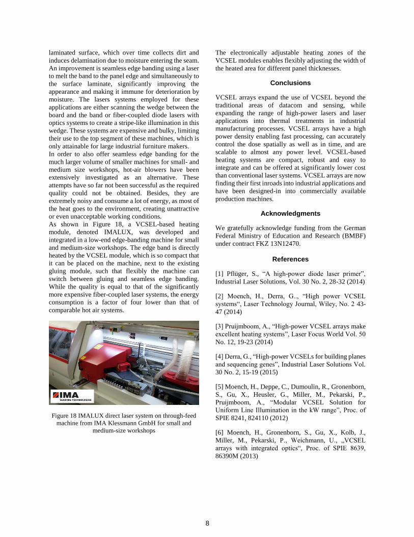
As shown in Figure 18, a VCSEL-based heating
module, denoted IMALUX, was developed and
integrated in a low-end edge-banding machine for small
and medium-size workshops. The edge band is directly
heated by the VCSEL module, which is so compact that
it can be placed on the machine, next to the existing
gluing module, such that flexibly the machine can
switch between gluing and seamless edge banding.
While the quality is equal to that of the significantly
more expensive fiber-coupled laser systems, the energy
consumption is a factor of four lower than that of
comparable hot air systems.
Figure 18 IMALUX direct laser system on through-feed
machine from IMA Klessmann GmbH for small and
medium-size workshops
The electronically adjustable heating zones of the
VCSEL modules enables flexibly adjusting the width of
the heated area for different panel thicknesses.
Conclusions
VCSEL arrays expand the use of VCSEL beyond the
traditional areas of datacom and sensing, while
expanding the range of high-power lasers and laser
applications into thermal treatments in industrial
manufacturing processes. VCSEL arrays have a high
power density enabling fast processing, can accurately
control the dose spatially as well as in time, and are
scalable to almost any power level. VCSEL-based
heating systems are compact, robust and easy to
integrate and can be offered at significantly lower cost
than conventional laser systems. VCSEL arrays are now
finding their first inroads into industrial applications and
have been designed-in into commercially available
production machines.
Acknowledgments
We gratefully acknowledge funding from the German
Federal Ministry of Education and Research (BMBF)
under contract FKZ 13N12470.
References
[1] Pflüger, S., “A high-power diode laser primer”,
Industrial Laser Solutions, Vol. 30 No. 2, 28-32 (2014)
[2] Moench, H., Derra, G.., “High power VCSEL
systems“, Laser Technology Journal, Wiley, No. 2 43-
47 (2014)
[3] Pruijmboom, A., “High-power VCSEL arrays make
excellent heating systems”, Laser Focus World Vol. 50
No. 12, 19-23 (2014)
[4] Derra, G., “High-power VCSELs for building planes
and sequencing genes”, Industrial Laser Solutions Vol.
30 No. 2, 15-19 (2015)
[5] Moench, H., Deppe, C., Dumoulin, R., Gronenborn,
S., Gu, X., Heusler, G., Miller, M., Pekarski, P.,
Pruijmboom, A., “Modular VCSEL Solution for
Uniform Line Illumination in the kW range”, Proc. of
SPIE 8241, 824110 (2012)
[6] Moench, H., Gronenborn, S., Gu, X., Kolb, J.,
Miller, M., Pekarski, P., Weichmann, U., „VCSEL
arrays with integrated optics“, Proc. of SPIE 8639,
86390M (2013)
8