variation-tolerant circuits: circuit solutions and techniques jim tschanz, keith bowman, and vivek...
TRANSCRIPT


Variation-Tolerant Circuits: Variation-Tolerant Circuits: Circuit Solutions and Circuit Solutions and
TechniquesTechniques
Variation-Tolerant Circuits: Variation-Tolerant Circuits: Circuit Solutions and Circuit Solutions and
TechniquesTechniques
Jim Tschanz, Keith Bowman, and Vivek DeJim Tschanz, Keith Bowman, and Vivek De
Microprocessor Technology LabMicroprocessor Technology LabIntel Corporation, Hillsboro, OregonIntel Corporation, Hillsboro, Oregon

OutlineOutline
Variations overviewVariations overview Process variationsProcess variations Impact of design choicesImpact of design choices Voltage and temperature variationsVoltage and temperature variations
Circuit techniquesCircuit techniques Adaptive body biasAdaptive body bias Adaptive supply voltageAdaptive supply voltage
Future trends & conclusionFuture trends & conclusion

Process VariationsProcess Variations
0.9
1.0
1.1
1.2
1.3
1.4
0 5 10 15 20
Normalized Leakage (Isb)N
orm
aliz
ed F
req
ue
nc
y
0.18 micron~1000 samples
20X
30%
0.9
1.0
1.1
1.2
1.3
1.4
0 5 10 15 20
Normalized Leakage (Isb)N
orm
aliz
ed F
req
ue
nc
y
0.18 micron~1000 samples
20X
30%
1980 1990 2000 2010 2020
100nm
1m
10nm
1980 1990 2000 2010 20201980 1990 2000 2010 2020
100nm
1m
10nm
193nm193nm248nm248nm
365nm365nmLithographyLithographyWavelengthWavelength
65nm65nm
90nm90nm
130nm130nm
GenerationGeneration
GapGap
45nm45nm
32nm32nm
180nm180nm
13nm 13nm EUVEUV
Sub-wavelength lithography
Effect of process variations
• Functionality & Yield• Performance• Power
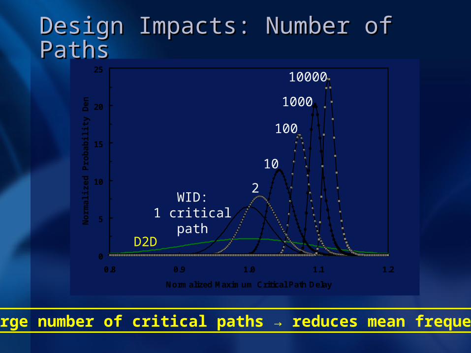
Design Impacts: Number of PathsDesign Impacts: Number of Paths
0
5
10
15
20
25
0.8 0.9 1.0 1.1 1.2
Normalized Maximum Critical Path Delay
No
rmal
ized
Pro
bab
ility
Den
sity
D2D
WID: Ncp=1
WID: Ncp=2
WID: Ncp=10
WID: Ncp=100
WID: Ncp=1000
WID: Ncp=10000
Large number of critical paths → reduces mean frequency
WID:1 critical path
2
10
100
1000
10000
D2D

Design Impacts: Logic DepthDesign Impacts: Logic Depth
10
100
1000
10000
1000 500 250 130 65 32
Technology Node (nm)
Me
an
Nu
mb
er
of
Do
pa
nt
Ato
ms
0.0
0.5
1.0
Logic depth
Rat
io o
fd
ela
y-
to Io
n-
16 490.0
0.5
1.0
Logic depth
Rat
io o
fd
ela
y-
to Io
n-
16 49
Random dopant fluctuation:Number of dopant atoms
Variation vs. depth
Reducing logic depth increases impact of random variations

Effect of Within-Die VariationsEffect of Within-Die Variations
0
20
40
60
80
100
-4 -3 -2 -1 0 1 2 3 4
Number of FMAX Standard Deviations
Cu
mu
lati
ve D
istr
ibu
tio
n (
%)
Measured DataModel: D2D & WIDModel: D2DModel: WID
Model: Only WID Variations
Model: Only D2D Variations
Model: D2D & WID Variations
D2D variations: impact varianceWID variations: reduce the mean FMAX

Voltage and Temperature Voltage and Temperature VariationsVariations
Time (us)
20 4 6 8 10 12 14 16 18 201.401.451.501.551.601.651.701.751.80
Vcc
Voltage droop
Temp(oC)
core
cache 70C
120C
Thermal profile
Variations are both static and dynamicStatic: Tools required for predictionDynamic: Design margining or adaptation techniques
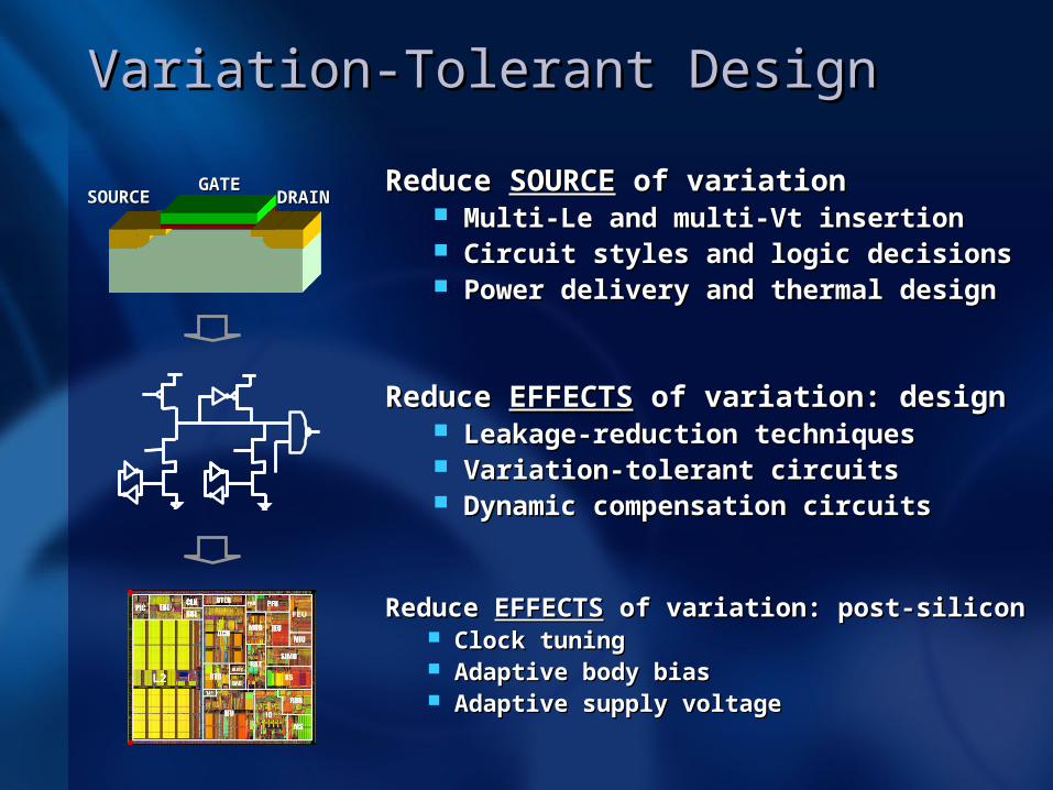
Variation-Tolerant DesignVariation-Tolerant Design
GATEGATESOURCESOURCE DRAINDRAIN
Reduce Reduce EFFECTSEFFECTS of variation: post-silicon of variation: post-silicon Clock tuningClock tuning Adaptive body biasAdaptive body bias Adaptive supply voltageAdaptive supply voltage
Reduce Reduce EFFECTSEFFECTS of variation: design of variation: design Leakage-reduction techniquesLeakage-reduction techniques Variation-tolerant circuitsVariation-tolerant circuits Dynamic compensation circuitsDynamic compensation circuits
Reduce Reduce SOURCESOURCE of variation of variation Multi-Le and multi-Vt insertionMulti-Le and multi-Vt insertion Circuit styles and logic decisionsCircuit styles and logic decisions Power delivery and thermal designPower delivery and thermal design
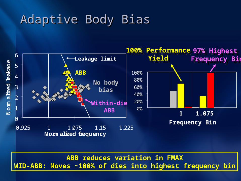
Adaptive Body BiasAdaptive Body Bias
0
1
2
3
4
5
6
0.925 1 1.075 1.15 1.225Normalized frequency
No
rmali
zed
leakag
e
ABB
Within-dieABB
No bodybias
Leakage limit
ABB reduces variation in FMAXWID-ABB: Moves ~100% of dies into highest frequency bin
0%
20%
40%
60%
80%
100%
1 1.075
Frequency Bin
100% PerformanceYield
100% PerformanceYield
97% Highest Frequency Bin
97% Highest Frequency Bin

Adaptive Supply VoltageAdaptive Supply Voltage
79%
3%16%
2%
71%
26%
0%
20%
40%
60%
80%
100%
0.9 0.95 1 1.05Frequency Bin
Die
Co
un
t
Fixed VDD: 1.05V
Adaptive VDD6%
37%52%
10%
74%
15%
0%
20%
40%
60%
80%
100%
0.9 0.95 1 1.05Frequency Bin
Die
Co
un
t
Fixed VDD: 1.05V
Adaptive VDD6%
37%52%
10%
74%
15%
0%
20%
40%
60%
80%
100%
0.9 0.95 1 1.05Frequency Bin
Die
Co
un
t
Adaptive VBS
Adaptive VDD + VBS
Adaptive VDD + VBS is most effective
90 100 110 120 130 1400
10
20
30
40
50
90 100 110 120 130 1400
10
20
30
40
50
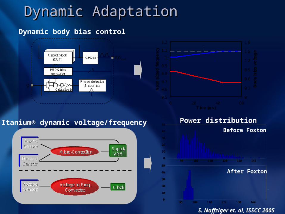
Dynamic AdaptationDynamic Adaptation
PMOS bias generator
Phase detector & counter
Critical path
divider ROout
Circuit block (CUT)
5
0.5
0.6
0.7
0.8
0.9
1
1.1
1.2
0 20 40 60Time (ms)
No
rmal
ized
fre
qu
ency
0
0.3
0.6
0.9
1.2
1.5
1.8
Bo
dy
bia
s v
olt
ag
e
PMOS body voltage
Frequency
Frequency target
MicroMicro--ControllerController
PowerPowerSensorSensor
SupplySupplyVRMVRM
ThermalThermalSensorSensor
VoltageVoltageSensorSensor
Voltage to Freq.Voltage to Freq.Converter Converter ClockClock
Dynamic body bias control
Itanium® dynamic voltage/frequency
0
10
20
30
40
50
90 100 110 120 130 1400
10
20
30
40
50
90 100 110 120 130 140
Power distributionBefore Foxton
After Foxton
S. Naffziger et. al, ISSCC 2005

Future Circuit TrendsFuture Circuit Trends
Variation-centric designVariation-centric design Probabalistic timing and optimizationProbabalistic timing and optimization Variation-tolerant circuit stylesVariation-tolerant circuit styles Microarchitecture supportMicroarchitecture support
Dynamic adaptationDynamic adaptation Reduce design margins requiredReduce design margins required Supply voltage droopsSupply voltage droops Temperature changesTemperature changes Reliability effectsReliability effects

ConclusionConclusion
Impact of variations is increasingImpact of variations is increasing Aggressive feature size scalingAggressive feature size scaling Increased die size and number of pathsIncreased die size and number of paths Design margins are increasingDesign margins are increasing
Variation-aware design neededVariation-aware design needed Variation-tolerant circuitsVariation-tolerant circuits Post-silicon tuning techniquesPost-silicon tuning techniques Supported by device, circuit, and Supported by device, circuit, and
microarchitecture innovationsmicroarchitecture innovations