vanel jean-charles llr / in2p3 nikhef 1-4 april 2003 nikhef 1-4 april 2003 technical status of the...
TRANSCRIPT

Vanel Jean-Charles LLR / IN2P3Vanel Jean-Charles LLR / IN2P3 NIKHEF 1-4 April 2003NIKHEF 1-4 April 2003
Technical status of the W-Si Technical status of the W-Si project project CALICE : CALICE : CACAlorimeter for the lorimeter for the LILInear near CCollider with ollider with
EElectronslectrons A calorimeter optimized for the Energy Flow A calorimeter optimized for the Energy Flow measurement of multi-jets final state at the Future measurement of multi-jets final state at the Future Linear Collider running at a center-of-mass energy Linear Collider running at a center-of-mass energy between 90 GeV to 1 TeV.between 90 GeV to 1 TeV.
Electromagnetic CalorimeterElectromagnetic Calorimeter Hadronic CalorimeterHadronic Calorimeter
http://polywww.in2p3.fr/flc/calice.html

Vanel Jean-Charles LLR / IN2P3Vanel Jean-Charles LLR / IN2P3 NIKHEF 1-4 April 2003NIKHEF 1-4 April 2003
General view of the General view of the calorimetercalorimeter Tracker : TPCTracker : TPC
ECAL : Sandwich Wplate & Si WaferECAL : Sandwich Wplate & Si WaferHCAL : DHCAL or AHCALHCAL : DHCAL or AHCALCoil : 4 T (2 Coil : 4 T (2 ))

Vanel Jean-Charles LLR / IN2P3Vanel Jean-Charles LLR / IN2P3 NIKHEF 1-4 April 2003NIKHEF 1-4 April 2003
ECAL concept : ECAL concept :
- A A fine granularity calorimeter with large number of segmentationfine granularity calorimeter with large number of segmentation is is proposed as the best solution for the energy flow, lepton identification, proposed as the best solution for the energy flow, lepton identification, photon reconstruction with good precision on energy and direction.photon reconstruction with good precision on energy and direction.
- On the other side, the coil thickness is bigger than usual due to the 4 On the other side, the coil thickness is bigger than usual due to the 4 Tesla field needed to maintain the machine background close to the Tesla field needed to maintain the machine background close to the beam pipe. beam pipe. Therefore , the ECAL has to be very compact. (1,30 m for Therefore , the ECAL has to be very compact. (1,30 m for ECAL and HCAL)ECAL and HCAL)
- Such a calorimeter could be made of Such a calorimeter could be made of Tungsten-Silicon sandwichTungsten-Silicon sandwich..- With pad of 1x1 cm and 40 layers : With pad of 1x1 cm and 40 layers : A TRACKER CALORIMETERA TRACKER CALORIMETER . .
- It gives a clean picture of all energy flow objects in all type of eventsIt gives a clean picture of all energy flow objects in all type of events- Simulation using GEANT4 lead to think of an energy resolution on Simulation using GEANT4 lead to think of an energy resolution on
electron/photon in the region of Delta E /E = 11% / sqrt(E) electron/photon in the region of Delta E /E = 11% / sqrt(E)

Vanel Jean-Charles LLR / IN2P3Vanel Jean-Charles LLR / IN2P3 NIKHEF 1-4 April 2003NIKHEF 1-4 April 2003
Toward physique Toward physique prototype :prototype :

Vanel Jean-Charles LLR / IN2P3Vanel Jean-Charles LLR / IN2P3 NIKHEF 1-4 April 2003NIKHEF 1-4 April 2003
ECAL general view
3rd structure (3×1.4mm of W plates)
370 mm
180 mm
Silicon wafer
2nd structure (2×1.4mm of W plates)
VME/…
HCAL
VFEMovable table
ECALBeam
monitoring
Global view of the test beam setup
Prototypes Prototypes overviewoverview
BEAM
1st structure (1.4mm of W plates)
Detector slab
370 mm

Vanel Jean-Charles LLR / IN2P3Vanel Jean-Charles LLR / IN2P3 NIKHEF 1-4 April 2003NIKHEF 1-4 April 2003
Design and construction of a mould with all metallic pieces for the 3 different structures
Mould for alveolus structure 1.4
Alveolus structuresAlveolus structures
Structure 5 alveolus :(10 layers)
Detector slab (here it is just a type H structure)

Vanel Jean-Charles LLR / IN2P3Vanel Jean-Charles LLR / IN2P3 NIKHEF 1-4 April 2003NIKHEF 1-4 April 2003
Sizes of the structure : Sizes of the structure : AlveolusAlveolus
8.5 mm8.5 mm
125
.6 m
m1
25
.6 m
m
374.5 mm
374.5 mm

Vanel Jean-Charles LLR / IN2P3Vanel Jean-Charles LLR / IN2P3 NIKHEF 1-4 April 2003NIKHEF 1-4 April 2003
Front End electronics
(Cfi / W) structure type H
Silicon wafer
Shielding
PCB
Al. ShieldingPCB (multi-layers)
( 2.4 mm)
Silicon wafer(0.525 mm)
Tungsten(1.4 mm, 2×1.4 or 3×1.4 mm)
8.5
mm
Composite structure (0.15 mm / layer)
Transverse view
Detector slabDetector slab
PCB : PCB :
- 14 layers14 layers
- Thickness 2.4 mmThickness 2.4 mm

Vanel Jean-Charles LLR / IN2P3Vanel Jean-Charles LLR / IN2P3 NIKHEF 1-4 April 2003NIKHEF 1-4 April 2003
Type H structure Type H structure
Carbon fiber
Tungsten 1.4 mm thick
Conception and realization of mould for manufacturing the whole 30 type H structures (3 different thickness W) :
Mould structure H : Ended alveolar :

Vanel Jean-Charles LLR / IN2P3Vanel Jean-Charles LLR / IN2P3 NIKHEF 1-4 April 2003NIKHEF 1-4 April 2003
Sizes of the structure : Sizes of the structure : SlabSlab
8,3
mm
8,3
mm
Aluminum foil : ~0.1 mmAluminum foil : ~0.1 mm
PCB : 2.4 mmPCB : 2.4 mm
Wafer : 0.525 mmWafer : 0.525 mm
Carbon fiber : 0.15 mmCarbon fiber : 0.15 mm
W plate : 1.4 mmW plate : 1.4 mm

Vanel Jean-Charles LLR / IN2P3Vanel Jean-Charles LLR / IN2P3 NIKHEF 1-4 April 2003NIKHEF 1-4 April 2003
PCBPCB
PCB, Wafer, Chip : still in progressPCB, Wafer, Chip : still in progress

Vanel Jean-Charles LLR / IN2P3Vanel Jean-Charles LLR / IN2P3 NIKHEF 1-4 April 2003NIKHEF 1-4 April 2003
WaferWaferWaferWafer
PCBPCB
PCB, Wafer, Chip : still in progressPCB, Wafer, Chip : still in progress

Vanel Jean-Charles LLR / IN2P3Vanel Jean-Charles LLR / IN2P3 NIKHEF 1-4 April 2003NIKHEF 1-4 April 2003
PCBPCB
ChipChipChipChip
PCB, Wafer, Chip : still in progressPCB, Wafer, Chip : still in progress
Vanel Jean-Charles LLR / IN2P3Vanel Jean-Charles LLR / IN2P3 NIKHEF 1-4 April 2003NIKHEF 1-4 April 2003
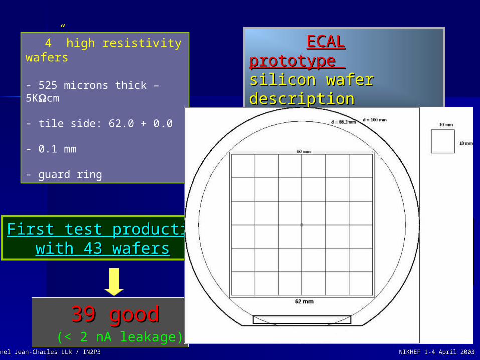
4” high resistivity wafers
- 525 microns thick – 5Kcm
- tile side: 62.0 + 0.0 - 0.1 mm
- guard ring
ECAL prototype ECAL prototype silicon wafer silicon wafer descriptiondescription
Dead zone w
idth is
only 1mm
39 good 39 good (< 2 nA leakage)
First test production First test production with 43 waferswith 43 wafers

Vanel Jean-Charles LLR / IN2P3Vanel Jean-Charles LLR / IN2P3 NIKHEF 1-4 April 2003NIKHEF 1-4 April 2003
Wafer :Wafer :
0
1
2
3
4
5
6
7
8
00,
40,
81,
21,
6 22,
42,
83,
23,
6
Nu
mb
er
of
pa
ds
,00%
20,00%
40,00%
60,00%
80,00%
100,00%
120,00%
Fréquence % cumulé
Leakage curent (nA)Leakage curent (nA)
Thickness : 525 microns Thickness : 525 microns 3 % 3 %
In silicon ~80 e-h pairs / micron In silicon ~80 e-h pairs / micron 42000 e42000 e-- /MiP/MiP
Capacitance : ~25 pFCapacitance : ~25 pF
Leakage current : 1 – 5 nALeakage current : 1 – 5 nA
Full depletion bias : ~150 VFull depletion bias : ~150 V
Nominal operating bias : 200 VNominal operating bias : 200 V
Institute of Nuclear Physics - Moscow State University
Institute of Physics, Academy of Sciences of the Czech Republic - Prague

Vanel Jean-Charles LLR / IN2P3Vanel Jean-Charles LLR / IN2P3 NIKHEF 1-4 April 2003NIKHEF 1-4 April 2003
1 wafer
62mm
62mm
PCBWafers
The aluminium sheet is the ground
Aluminium sheet
10mm
10mm
2 2 2 2 2
2
6
Diode footprint
Detector schematic descriptionDetector schematic descriptionAmorphous silicon deposition Resistance
Capacitance (AC coupling)
Yvan BonnasieuxYvan BonnasieuxPhysique des Interfaces et Couches Minces Physique des Interfaces et Couches Minces
- Ecole Polytechnique - Palaiseau- Ecole Polytechnique - Palaiseau
Diode pin out
Diode bias
Sig. readout

Vanel Jean-Charles LLR / IN2P3Vanel Jean-Charles LLR / IN2P3 NIKHEF 1-4 April 2003NIKHEF 1-4 April 2003
Passive component on the Passive component on the wafer :wafer :
R
C
1 0
1 0
0,1 0,1
2
0,1
0,2
7,6
9,8
Capacitance : Dielectric : silicon nitrite Refractive index : n=2 Thickness : e = 2 m
rn
Resistance : material : aSiH Resistivity : =1011 .cm Thickness : l = 2 m
e
SC
r0
S
lR
C= 1,32 nF
R= 102 M

Vanel Jean-Charles LLR / IN2P3Vanel Jean-Charles LLR / IN2P3 NIKHEF 1-4 April 2003NIKHEF 1-4 April 2003
Passive component on the Passive component on the wafer :wafer :
-0,6
-0,4
-0,2
0
0,2
0,4
0,6
-300 -200 -100 0 100 200 300
Tension (V)
curr
ent
(nA
)
Capacitance : C ~ 1.4 nF Leakage current
Problem of measurement
Resistance : Still in progress …

Vanel Jean-Charles LLR / IN2P3Vanel Jean-Charles LLR / IN2P3 NIKHEF 1-4 April 2003NIKHEF 1-4 April 2003
Gluing of Si waferGluing of Si waferA automatic device is use to deposit the conductive glue :
X-Y-Z table (400×400×150 mm3) with glue dispensing tool (conductive glue)
Gluing and placement ( 0.1 mm) of 270270 wafers with 6×6 pads
About 10 00010 000 points of glue.

Vanel Jean-Charles LLR / IN2P3Vanel Jean-Charles LLR / IN2P3 NIKHEF 1-4 April 2003NIKHEF 1-4 April 2003
Vdc = -200V
DC block
Detector
Amp
Charge preamp
OPA
shaper Track & hold
Front end electronic : Front end electronic : AsicAsic Laboratoire de l'Accélérateur Linéaire - OrsayLaboratoire de l'Accélérateur Linéaire - Orsay

Vanel Jean-Charles LLR / IN2P3Vanel Jean-Charles LLR / IN2P3 NIKHEF 1-4 April 2003NIKHEF 1-4 April 2003
Vdc = -200V
DC block
Detector
Amp
Charge preamp
OPA
shaper Track & hold
Front end electronic : Front end electronic : AsicAsic
4.2 pC max input charge (650 MIP)2.8V dynamic rangebelow 1% non-linearity
4.2 pC max input charge (650 MIP)2.8V dynamic rangebelow 1% non-linearity
Laboratoire de l'Accélérateur Linéaire - OrsayLaboratoire de l'Accélérateur Linéaire - Orsay

Vanel Jean-Charles LLR / IN2P3Vanel Jean-Charles LLR / IN2P3 NIKHEF 1-4 April 2003NIKHEF 1-4 April 2003
Vdc = -200V
DC block
Detector
Amp
Charge preamp
OPA
shaper Track & hold
Front end electronic : Front end electronic : AsicAsic
180ns peaking time
Laboratoire de l'Accélérateur Linéaire - OrsayLaboratoire de l'Accélérateur Linéaire - Orsay

Vanel Jean-Charles LLR / IN2P3Vanel Jean-Charles LLR / IN2P3 NIKHEF 1-4 April 2003NIKHEF 1-4 April 2003
Vdc = -200V
DC block
Detector
Amp
Charge preamp
OPA
shaper Track & hold
Front end electronic : Front end electronic : AsicAsic
Multiplexing output :Multiplexing output :18 channel / chip18 channel / chip2 chips / wafer2 chips / waferENC = 2200 @ 80 pFENC = 2200 @ 80 pF
Multiplexing output :Multiplexing output :18 channel / chip18 channel / chip2 chips / wafer2 chips / waferENC = 2200 @ 80 pFENC = 2200 @ 80 pF
Laboratoire de l'Accélérateur Linéaire - OrsayLaboratoire de l'Accélérateur Linéaire - Orsay
Talk from Bernard Bouquet : R&D for ECAL-VFE technology prototype
Vanel Jean-Charles LLR / IN2P3Vanel Jean-Charles LLR / IN2P3 NIKHEF 1-4 April 2003NIKHEF 1-4 April 2003
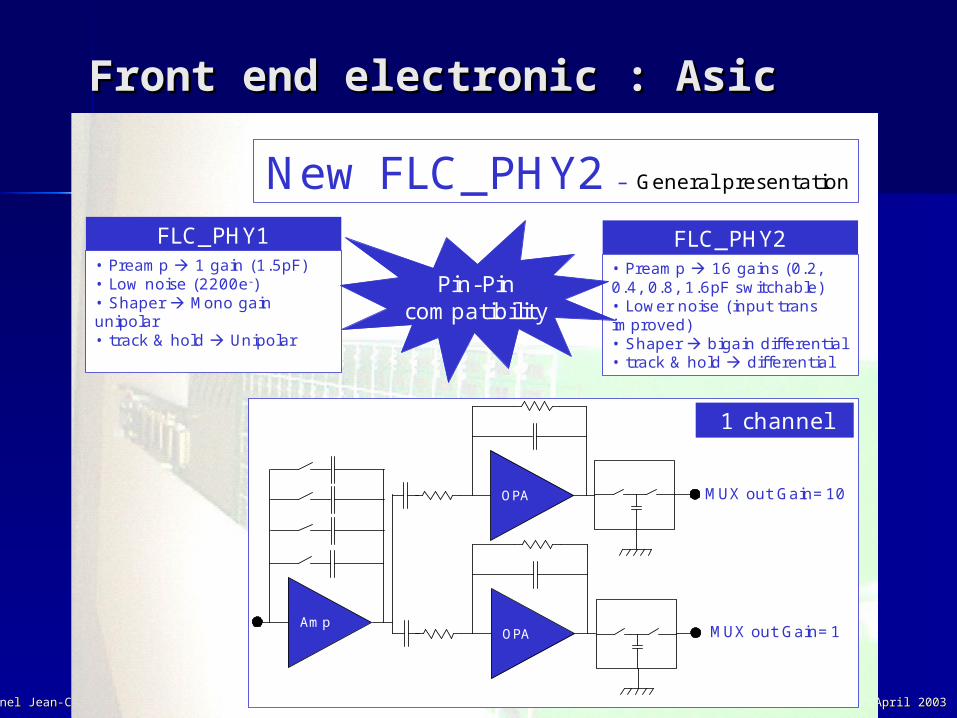
Front end electronic : AsicFront end electronic : Asic
New FLC_PHY2 – General presentation
FLC_PHY1 FLC_PHY2• Preamp 16 gains (0.2, 0.4, 0.8, 1.6pF switchable)• Lower noise (input transimproved)• Shaper bigain differential• track & hold differential
• Preamp 1 gain (1.5pF)• Low noise (2200e-)• Shaper Mono gainunipolar• track & hold Unipolar
Pin-Pincompatibility
AmpOPA
OPA
MUX out Gain=1
MUX out Gain=10
1 channel

Vanel Jean-Charles LLR / IN2P3Vanel Jean-Charles LLR / IN2P3 NIKHEF 1-4 April 2003NIKHEF 1-4 April 2003
New FLC_PHY2
• Peaking time is 200ns on both gain•High-gain shapers can be shut down by switching off their biases•Two different output for low gain and high gainInterface compatibility with the read out is keptNew interface not written at this point
Linearity simulationTransient simulation

Vanel Jean-Charles LLR / IN2P3Vanel Jean-Charles LLR / IN2P3 NIKHEF 1-4 April 2003NIKHEF 1-4 April 2003
DAQ :DAQ : VME (use and modify CMS board for Si VME (use and modify CMS board for Si
tracker)tracker)
21 January 2003 Paul Dauncey - UK Electronics 1
FED layoutIdeally, keep everything to the right, redo everything to the left
• Restrictsreadout board to same I/O and inter-FPGA paths as FED
• No major problems seen so far
Need of 6 boards for physic prototypeNeed of 6 boards for physic prototypeNeed of 6 boards for physic prototypeNeed of 6 boards for physic prototype
Talk from Paul Dauncey : DAQ for the CALICE beam test

Vanel Jean-Charles LLR / IN2P3Vanel Jean-Charles LLR / IN2P3 NIKHEF 1-4 April 2003NIKHEF 1-4 April 2003
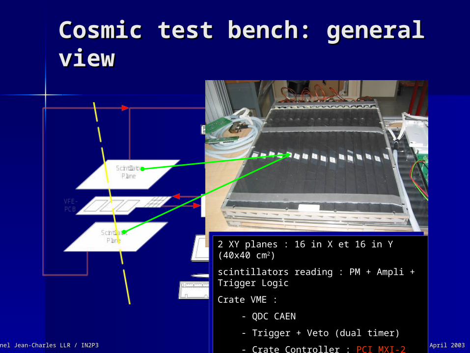
Cosmic test bench: general Cosmic test bench: general viewview
Vanel Jean-Charles LLR / IN2P3Vanel Jean-Charles LLR / IN2P3 NIKHEF 1-4 April 2003NIKHEF 1-4 April 2003
2 XY planes : 16 in X et 16 in Y (40x40 cm2 XY planes : 16 in X et 16 in Y (40x40 cm22))
scintillators reading : PM + Ampli + Trigger scintillators reading : PM + Ampli + Trigger LogicLogic
Crate VME :Crate VME :
- QDC CAENQDC CAEN
- Trigger + Veto (dual timer)Trigger + Veto (dual timer)
- Crate Controller : Crate Controller : PCI MXI-2 (NI) PCI MXI-2 (NI) boardboard
Cosmic test bench: general Cosmic test bench: general viewview

Vanel Jean-Charles LLR / IN2P3Vanel Jean-Charles LLR / IN2P3 NIKHEF 1-4 April 2003NIKHEF 1-4 April 2003
Cosmic test bench: general Cosmic test bench: general viewview
Pattern generation board Pattern generation board (Labo)(Labo) : :Numerical CPLDNumerical CPLDClock toward PCB : 208 KHzClock toward PCB : 208 KHz
Level translator TTL/RS422Level translator TTL/RS422
Pattern generation board Pattern generation board (Labo)(Labo) : :Numerical CPLDNumerical CPLDClock toward PCB : 208 KHzClock toward PCB : 208 KHz
Level translator TTL/RS422Level translator TTL/RS422

Vanel Jean-Charles LLR / IN2P3Vanel Jean-Charles LLR / IN2P3 NIKHEF 1-4 April 2003NIKHEF 1-4 April 2003
Cosmic test bench: general Cosmic test bench: general viewview
Talk from Cristina Lo Bianco : Assembly and cosmic test for the W-SI prototype (CALICE)
Commercial board (National Instrument)Commercial board (National Instrument) - PCI Interface- PCI Interface - ADC 12 bits (1.25 Msa/s)- ADC 12 bits (1.25 Msa/s) - DMA Transfer- DMA Transfer - Input dynamic : from +/- 0.05 to +/- - Input dynamic : from +/- 0.05 to +/- 10V10V
Commercial board (National Instrument)Commercial board (National Instrument) - PCI Interface- PCI Interface - ADC 12 bits (1.25 Msa/s)- ADC 12 bits (1.25 Msa/s) - DMA Transfer- DMA Transfer - Input dynamic : from +/- 0.05 to +/- - Input dynamic : from +/- 0.05 to +/- 10V10V

Vanel Jean-Charles LLR / IN2P3Vanel Jean-Charles LLR / IN2P3 NIKHEF 1-4 April 2003NIKHEF 1-4 April 2003
Other ECAL R&D Other ECAL R&D
Thermal studiesThermal studies VFE inside beamVFE inside beam
(Chip evaluation board and small DAQ are (Chip evaluation board and small DAQ are ready)ready)
Passive component on the wafer Passive component on the wafer (Capacitance Ok and resistance still in progress)(Capacitance Ok and resistance still in progress)
Amorphous silicon … (works of Amorphous silicon … (works of Pierre Jarron at Cern)Pierre Jarron at Cern)
……

Vanel Jean-Charles LLR / IN2P3Vanel Jean-Charles LLR / IN2P3 NIKHEF 1-4 April 2003NIKHEF 1-4 April 2003
Other ECAL R&D Other ECAL R&D
Thermal studiesThermal studies
Pad
Silicon wafer
PCB
Aluminium
Cooling tube Cooling tubeVFE chip1.3 mm
1.0 mm
0.5 mm
Thermal contact
gluing for electrical contact
AC coupling elements ?
power linecommand linesignal out
Pad
Silicon wafer
PCB
Aluminium
Cooling tube Cooling tubeVFE chip1.3 mm
1.0 mm
0.5 mm
Thermal contact
gluing for electrical contact
AC coupling elements ?
power linecommand linesignal out

Vanel Jean-Charles LLR / IN2P3Vanel Jean-Charles LLR / IN2P3 NIKHEF 1-4 April 2003NIKHEF 1-4 April 2003
Other ECAL R&D Other ECAL R&D
Thermal studiesThermal studies
In the case of 40 layers and In the case of 40 layers and considering a power considering a power dissipated of about 5 mW/cmdissipated of about 5 mW/cm22 the temperature at the the temperature at the middle of structure would be middle of structure would be about about 280 °C280 °C

Vanel Jean-Charles LLR / IN2P3Vanel Jean-Charles LLR / IN2P3 NIKHEF 1-4 April 2003NIKHEF 1-4 April 2003
Other ECAL R&D Other ECAL R&D
Thermal studiesThermal studies
PCB 1mm thick(with wafers)
Heat points(VFE chip)
Cooling channel
Radiator aluminium plate
Structure type H
Thermal sensors
Externalconnections

Vanel Jean-Charles LLR / IN2P3Vanel Jean-Charles LLR / IN2P3 NIKHEF 1-4 April 2003NIKHEF 1-4 April 2003
Other ECAL R&D Other ECAL R&D
Thermal studiesThermal studies VFE inside beamVFE inside beam
(Chip evaluation board and small DAQ are (Chip evaluation board and small DAQ are ready)ready)
Passive component on the wafer Passive component on the wafer (Capacitance Ok and resistance still in progress)(Capacitance Ok and resistance still in progress)
Amorphous silicon … (works of Amorphous silicon … (works of Pierre Jarron at Cern)Pierre Jarron at Cern)
……

Vanel Jean-Charles LLR / IN2P3Vanel Jean-Charles LLR / IN2P3 NIKHEF 1-4 April 2003NIKHEF 1-4 April 2003
Physic prototype : Physic prototype : who who ??
Mechanic : Mechanic : – W plates : RussianW plates : Russian– ECAL Structure : ECAL Structure : LLRLLR– Infrastructure of beam test : Infrastructure of beam test : LPC Clermont-ferrand ? LPC Clermont-ferrand ? and and ??– beam Hodoscope : beam Hodoscope : ??
Data processing : Data processing : – DAQ / Event Builder : DAQ / Event Builder : ??– Simulation : Simulation : LLRLLR
Electronic : Electronic : – VFE : VFE : LALLAL– DAQ : DAQ : UKUK– Slow control : Slow control : ??
Instrumentation :Instrumentation :– silicon : silicon : LLRLLR and and PICM + Russian and CzechPICM + Russian and Czech– ECAL Integration :ECAL Integration : LLRLLR– Cosmic test bench : Cosmic test bench : LLRLLR

Vanel Jean-Charles LLR / IN2P3Vanel Jean-Charles LLR / IN2P3 NIKHEF 1-4 April 2003NIKHEF 1-4 April 2003
Physic Prototype : Physic Prototype : PlanningPlanning

Vanel Jean-Charles LLR / IN2P3Vanel Jean-Charles LLR / IN2P3 NIKHEF 1-4 April 2003NIKHEF 1-4 April 2003
Physic Prototype : Physic Prototype : PlanningPlanning
ID Nom de tâcheQ2 04Q2 03 Q4 03Q1 03 Q1 04Q3 03
aoûmar févoctmai jan mar avrnov juijuljan maifév sep décavr
Prototype (design + layout + Fab.)
5 Gluing studies
Production (9 board)
Chip redisgn + Foundry + test
Cosmic test bench design + fab
Slow control
Event Builder19
DAQ14
Production VFE8
10
PCB design
DAQ
Event Builder
Slow control
Infrastructure test beam20 Infrastructure test beam
Assemblage et Montage11 Chip Production
Q3 04
juljui aoû
Production PCB9PCB fabrication + test +Production
Mecanic1 Mecanic
16
17
sep
15
Structure 1.42 Structure 1.4
Structure type H3 Structure type H
Structure 2.8 - 4.24 Structure 2.8 - 4.2
Assembly6 Assembly
Electronic VFE & PCB7 Electronic VFE & PCB
12 PCB & Chip assemnly
Cosmic test18 Cosmic test of slab detector
13
21 Beam test with electrons
Q4 04
oct nov déc

Vanel Jean-Charles LLR / IN2P3Vanel Jean-Charles LLR / IN2P3 NIKHEF 1-4 April 2003NIKHEF 1-4 April 2003
Physic Prototype : Physic Prototype : PlanningPlanning
ID Nom de tâcheQ2 04Q2 03 Q4 03Q1 03 Q1 04Q3 03
aoûmar févoctmai jan mar avrnov juijuljan maifév sep décavr
Prototype (design + layout + Fab.)
5 Gluing studies
Production (9 board)
Chip redisgn + Foundry + test
Cosmic test bench design + fab
Slow control
Event Builder19
DAQ14
Production VFE8
10
PCB design
DAQ
Event Builder
Slow control
Infrastructure test beam20 Infrastructure test beam
Assemblage et Montage11 Chip Production
Q3 04
juljui aoû
Production PCB9PCB fabrication + test +Production
Mecanic1 Mecanic
16
17
sep
15
Structure 1.42 Structure 1.4
Structure type H3 Structure type H
Structure 2.8 - 4.24 Structure 2.8 - 4.2
Assembly6 Assembly
Electronic VFE & PCB7 Electronic VFE & PCB
12 PCB & Chip assemnly
Cosmic test18 Cosmic test of slab detector
13
21 Beam test with electrons
Q4 04
oct nov décID Nom de tâcheQ2 04Q2 03 Q4 03Q1 03 Q1 04Q3 03
aoûmar févoctmai jan mar avrnov juijuljan maifév sep décavr
5 Gluing studies
Q3 04
juljui aoû
Mecanic1 Mecanic
sep
Structure 1.42 Structure 1.4
Structure type H3 Structure type H
Structure 2.8 - 4.24 Structure 2.8 - 4.2
Assembly6 Assembly
Q4 04
oct nov déc

Vanel Jean-Charles LLR / IN2P3Vanel Jean-Charles LLR / IN2P3 NIKHEF 1-4 April 2003NIKHEF 1-4 April 2003
Physic Prototype : Physic Prototype : PlanningPlanning
ID Nom de tâcheQ2 04Q2 03 Q4 03Q1 03 Q1 04Q3 03
aoûmar févoctmai jan mar avrnov juijuljan maifév sep décavr
Prototype (design + layout + Fab.)
5 Gluing studies
Production (9 board)
Chip redisgn + Foundry + test
Cosmic test bench design + fab
Slow control
Event Builder19
DAQ14
Production VFE8
10
PCB design
DAQ
Event Builder
Slow control
Infrastructure test beam20 Infrastructure test beam
Assemblage et Montage11 Chip Production
Q3 04
juljui aoû
Production PCB9PCB fabrication + test +Production
Mecanic1 Mecanic
16
17
sep
15
Structure 1.42 Structure 1.4
Structure type H3 Structure type H
Structure 2.8 - 4.24 Structure 2.8 - 4.2
Assembly6 Assembly
Electronic VFE & PCB7 Electronic VFE & PCB
12 PCB & Chip assemnly
Cosmic test18 Cosmic test of slab detector
13
21 Beam test with electrons
Q4 04
oct nov déc
ID Nom de tâcheQ2 04Q2 03 Q4 03Q1 03 Q1 04Q3 03
aoûmar févoctmai jan mar avrnov juijuljan maifév sep décavr
Chip redisgn + Foundry + test
Slow control
Production VFE2
4
PCB design
Slow control
Assemblage et Montage5 Chip Production
Q3 04
juljui aoû
Production PCB3PCB fabrication + test +Production
sep
Electronic VFE & PCB1 Electronic VFE & PCB
6 PCB & Chip assemnly
7
Q4 04
oct nov déc

Vanel Jean-Charles LLR / IN2P3Vanel Jean-Charles LLR / IN2P3 NIKHEF 1-4 April 2003NIKHEF 1-4 April 2003
Physic Prototype : Physic Prototype : PlanningPlanning
ID Nom de tâcheQ2 04Q2 03 Q4 03Q1 03 Q1 04Q3 03
aoûmar févoctmai jan mar avrnov juijuljan maifév sep décavr
Prototype (design + layout + Fab.)
5 Gluing studies
Production (9 board)
Chip redisgn + Foundry + test
Cosmic test bench design + fab
Slow control
Event Builder19
DAQ14
Production VFE8
10
PCB design
DAQ
Event Builder
Slow control
Infrastructure test beam20 Infrastructure test beam
Assemblage et Montage11 Chip Production
Q3 04
juljui aoû
Production PCB9PCB fabrication + test +Production
Mecanic1 Mecanic
16
17
sep
15
Structure 1.42 Structure 1.4
Structure type H3 Structure type H
Structure 2.8 - 4.24 Structure 2.8 - 4.2
Assembly6 Assembly
Electronic VFE & PCB7 Electronic VFE & PCB
12 PCB & Chip assemnly
Cosmic test18 Cosmic test of slab detector
13
21 Beam test with electrons
Q4 04
oct nov déc
ID Nom de tâcheQ2 04Q2 03 Q4 03Q1 03 Q1 04Q3 03
aoûmar févoctmai jan mar avrnov juijuljan maifév sep décavr
Prototype (design + layout + Fab.)
Production (9 board)
Cosmic test bench design + fab
Event Builder6
DAQ1 DAQ
Event Builder
Infrastructure test beam7 Infrastructure test beam
Q3 04
juljui aoû
3
4
sep
2
Cosmic test5 Cosmic test of slab detector
8 Beam test with electrons
Q4 04
oct nov déc

Vanel Jean-Charles LLR / IN2P3Vanel Jean-Charles LLR / IN2P3 NIKHEF 1-4 April 2003NIKHEF 1-4 April 2003
Physic Prototype : Physic Prototype : PlanningPlanning
ID Nom de tâcheQ2 04Q2 03 Q4 03Q1 03 Q1 04Q3 03
aoûmar févoctmai jan mar avrnov juijuljan maifév sep décavr
Prototype (design + layout + Fab.)
5 Gluing studies
Production (9 board)
Chip redisgn + Foundry + test
Cosmic test bench design + fab
Slow control
Event Builder19
DAQ14
Production VFE8
10
PCB design
DAQ
Event Builder
Slow control
Infrastructure test beam20 Infrastructure test beam
Assemblage et Montage11 Chip Production
Q3 04
juljui aoû
Production PCB9PCB fabrication + test +Production
Mecanic1 Mecanic
16
17
sep
15
Structure 1.42 Structure 1.4
Structure type H3 Structure type H
Structure 2.8 - 4.24 Structure 2.8 - 4.2
Assembly6 Assembly
Electronic VFE & PCB7 Electronic VFE & PCB
12 PCB & Chip assemnly
Cosmic test18 Cosmic test of slab detector
13
21 Beam test with electrons
Q4 04
oct nov déc

Vanel Jean-Charles LLR / IN2P3Vanel Jean-Charles LLR / IN2P3 NIKHEF 1-4 April 2003NIKHEF 1-4 April 2003
Physic prototype Physic prototype program is well advances
First test beam with electrons First test beam with electrons mi 2004mi 2004 First hadronic test beam First hadronic test beam 2005 2005
All is not covered :All is not covered :– Physic prototype in 2004Physic prototype in 2004– R&D (thermal et electronic)R&D (thermal et electronic)– ……
http://polywww.in2p3.fr/flc/calice.html