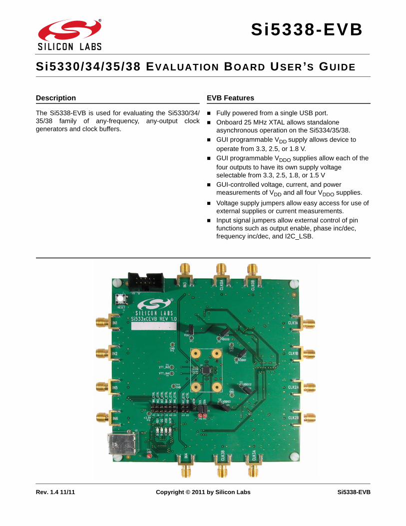
valuation board ser s uide · gui programmable vdd supply allows device to operate from 3.3, 2.5,...
TRANSCRIPT
Rev. 1.4 11/11 Copyright © 2011 by Silicon Labs Si5338-EVB
Si5338-EVB
Si5330/34/35/38 EVALUATION BOARD USER’S GUIDE
Description
The Si5338-EVB is used for evaluating the Si5330/34/35/38 family of any-frequency, any-output clockgenerators and clock buffers.
EVB Features
Fully powered from a single USB port.
Onboard 25 MHz XTAL allows standalone asynchronous operation on the Si5334/35/38.
GUI programmable VDD supply allows device to operate from 3.3, 2.5, or 1.8 V.
GUI programmable VDDO supplies allow each of the four outputs to have its own supply voltage selectable from 3.3, 2.5, 1.8, or 1.5 V
GUI-controlled voltage, current, and power measurements of VDD and all four VDDO supplies.
Voltage supply jumpers allow easy access for use of external supplies or current measurements.
Input signal jumpers allow external control of pin functions such as output enable, phase inc/dec, frequency inc/dec, and I2C_LSB.

Si5338-EVB
2 Rev. 1.4
1. Functional Block Diagram
A functional block diagram of the EVB is shown in Figure 1. The MCU performs the USB to I2C conversion,controls the voltage regulators, monitors the INTR pin, and controls the four status LEDS. It also provides control ofthe eight input pins when the INx_CTRL jumpers are populated. There are five programmable voltage regulators(VDD, VDDO0, VDDO1, VDDO2, VDDO3), which supply power to the Si533x device. VDD and VDDO jumpersallow the option of powering the device from external supplies, or as a convenient point for measuring current. I2Cjumpers allow disconnection of the Si533x device from the I2C bus to allow external control from another I2Cmaster.
For the Si5334, Si5335, and Si5338 devices, the EVB is shipped with an onboard 25 MHz XTAL to allowstand-alone asynchronous operation. For Si5335 emulation, synchronization to an external reference is done viaIN1 and IN2. Removal of the XTAL and addition of two 0 ohm resistors is required. IN3, IN4, IN5, and IN6 are notavailable as external clock inputs for Si5335.
Figure 1. EVB Functional Block Diagram
2. Quick Start
1. Install the ClockBuilder™ Desktop software and driver (assumes that Microsoft .NET Framework 1.1 is already installed).
2. Connect a USB cable from the EVB to the PC where the software was installed.
3. Leave the jumpers as installed from the factory, and launch the software by clicking on Start Programs Silicon Laboratories ClockBuilder Desktop. Click one of the shortcuts in the group.
XTAL
MCU
USB Connector
0
* indicates unpopulated components
IN1
0IN2
IN5
IN6
IN3
IN4
*
* CLK0A
CLK0B
VDDO0
VRegVReg
VRegVReg
CLK1A
CLK1B
VDDO1
term*term*
term*term*
CLK2A
CLK2B
VDDO2
term*term*
CLK3A
CLK3B
VDDO3
term*term*
Si5338
VReg
term*term*
VDD
To I2C Bus
IN7/SCL
IN8/SDA
INx_CTRL Jumpers
I2C
Bu
s
To I2C Bus
Status LEDs
Reset Switch
VDDO Jumpers
INTR
I2C Jumpers
VDD Jumpers

Si5338-EVB
Rev. 1.4 3
3. Jumpers
The Si5338-EVB is shipped with jumpers installed on the following positions:
VDD—Connects the Si533x VDD pin to the VDD programmable voltage regulator.
VDDO0—Connects the Si533x VDDO0 pin to the VDDO0 programmable voltage regulator.
VDDO1—Connects the Si533x VDDO1 pin to the VDDO1 programmable voltage regulator.
VDDO2—Connects the Si533x VDDO2 pin to the VDDO2 programmable voltage regulator.
VDDO3—Connects the Si533x VDDO3 pin to the VDDO3 programmable voltage regulator.
SCL—Connects the Si533x SCL pin to the I2C bus from the MCU.
SDA—Connects the Si533x SDA pin to the I2C bus from the MCU.
The INx-CTRL jumpers are optional jumpers for enabling MCU control of the Si533x input pins. This feature maybe available in future software releases.
4. Status LEDSThere are four status LEDs on the Si5338-EVB:
RDY (Green)—Indicates that the EVB is operating normally. This LED should always be on.
I2C (Green)—Indicates when there is active I2C communication between the MCU and the Si533x device or between the MCU and voltage regulators.
USB (Green)—Indicates when there is active communication between the PC and the MCU over the USB bus.
INTR (Red)—The MCU has detected that the interrupt pin of the Si533x device is enabled. The most probable cause for an interrupt is because the Si533x has lost its input signal or the PLL has lost lock. The “Status” tab of the GUI will identify the event that caused the interrupt to occur.

Si5338-EVB
4 Rev. 1.4
5. Inputs
The Si5338-EVB has six SMA connectors (IN1-IN6) for receiving external signals. Two of the signals aredifferential, and two are single-ended.
5.1. Differential Inputs (IN1/IN2, IN5/IN6)The differential inputs only need a differential voltage swing of 300 mV to operate, which makes them compatiblewith most differential signal types. See “AN408: Termination Options for Any-Frequency, Any-Output ClockGenerators and Clock Buffers—Si5338, Si5334, Si5330”, or Si5335 data sheet if applicable, for details oninterfacing with compatible signal types. It is also possible to lock the Si5334/35/38 to an external signal generatorusing one side of the differential input and grounding its complementary side. Take care not to exceed the maxdifferential voltage of 1.2 V on these inputs. The board is shipped with a 25 MHz XTAL connected to IN1/IN2. TheXTAL removal and resistor changes are required for Si5335 evaluation with an input clock since only IN1 and IN2are available for input clocking with Si5335. Note that regardless of device, any external input to IN1 & IN2 must belimited to 1.2 V peak-to-peak (see Figure 2 for resistor locations). When evaluating the Si5330, the XTAL must beremoved. The differential input on pins IN5/IN6 is ac-coupled with a 100 line termination (R39).
Figure 2. Optional Termination Resistors for Differential Inputs IN1/IN2
5.2. Single-Ended Inputs (IN3, IN4) [Not supported in Si5335]These inputs are dc-coupled to the device. They are compatible with a signal swing as low as 100 mV and amaximum of 3.63 V. The signal should have a minimum amount of dc bias to ensure that it is never below groundlevel.
The EVB provides pads for optional input terminations. These may be necessary when interfacing to SSTL andHSTL signals.
Note: For details on populated vs. non-populated components, refer to "9. Bill of Materials" on page 13.

Si5338-EVB
Rev. 1.4 5
6. Outputs (CLKxA/CLKxB)
Each of the four differential output drivers is capacitively coupled to the SMA connectors; so, the output signal willhave no dc bias. If a signal with dc bias is required, the ac coupling capacitors can be replaced with a 0 resistor.
The EVB provides pads for optional output terminations. These may be necessary when interfacing to SSTL andHSTL signals.
6.1. Evaluating LVPECL Output ClocksThe EVB by default is populated to allow evaluating of all output clock formats with the exception of LVPECLoutputs. To evaluate LVPECL signals on the Si5338-EVB, a few components must be soldered down on the board.Take CLK0 for example of. Note that CLK0 has R85, R121/R122, R1/R4, R2/R5, R3/R6, C4/C7, and C15/C17attached to the nets of interest. The EVB comes with only R121/R122 and C15/C17 installed. This allows supportof all output types except LVPECL.
Evaluating an ac-coupled LVPECL clock on CLK0 requires a bias resistor of 130 or 200 to ground on each of theoutput lines depending on driver VDDO. Refer to AN408, or Si5335 data sheet if applicable, for termination details.Make the following changes depending on the CLK0 VDDO voltage:
For 3.3 V LVPECL (ac-coupled)· Place 200 resistors in place of R1 and R4.· Place 0 resistors in place of C4 and C7.
For 2.5 V LVPECL (ac-coupled)· Place 130 resistors in place of R1 and R4.· Place 0 resistors in place of C4 and C7.
The LVPECL output may also be dc-coupled to an LVPECL receiver. To dc-couple the CLK0 output, make thecomponent changes below. Note that R2, R3, R5, and R6 depend on VDDO.
Place 0 resistors in place of C15 and C17.
Place 50 resistors in place of R1 and R4.
Place C4 and C7
Select R2 and R3 (and similarly R5 and R6) to give a termination voltage of VTT = VDDO – 2 V.
For LVPECL termination on CLK1, 2, and 3 follow the guidelines above and refer to the schematics in “8.Si5338-EVB Schematics” as needed.
6.2. Evaluating SSTL/HSTL Output ClocksTo support SSTL/HSTL outputs, either single-ended or differential, replace the output dc blocking capacitors with a0 resistor. For example, for CLK0 output, replace C15 with 0 resistor for single-ended, or replace both C15 &C17 with 0 for differential output. Do the same for CLK1,2,3 as needed. Remember to properly terminate at thereceiver input.
The Si5338-EVB can support on-board termination of SSTL/HSTL outputs, if on-board terminated, measurementof the clock output at the SMA connector would require a high impedance measurement device to preventoverloading of the output. If on-board output termination is desired, the following components must be installed(using CLK0 as an example.)
For 1.8 or 2.5 V VDDO: R2 = 2 k, R3 = 2 k, R1 = 50 , C4 = 0.1 µF
For 3.3 V VDDO: R2 = 2.42 k, R3 = 2 k, R1 = 50 , C4 = 0.1 µF
Follow similar guidelines for CLK1,2,3 as required. Refer to AN408, or Si5335 data sheet if applicable, for moredetails on clock termination.

Si5338-EVB
6 Rev. 1.4
7. ClockBuilder Desktop Software Installation
The following sections describe how to install and begin using the software. There is also a readme.txt file with theinstallation files as well as a user guide installed with the software.
Download the latest versions of the EVB documentation and the ClockBuilder Desktop software for this EVB byvisiting the following:
EVB User's Guide and documentation set: www.silabs.com/Si5338-EVB. ClockBuilder Desktop Software: www.silabs.com/ClockBuilder.
7.1. System RequirementsMicrosoft Windows 2000 or Windows XPUSB 2.02 MB of free hard drive space1024 x 768 screen resolution or greaterMicrosoft .NET Framework 1.1 USBXpress 3.1.1 driver
Note: USBXpress 3.1.1 driver is provided and installed with the software. Newer or older versions of USBXpress availablefrom other EVB kits or online have not been tested with this software.
7.2. Microsoft .NET Framework InstallationThe Microsoft .NET Framework is required before installing and running the software. Details and installationinformation about the .NET Framework are available via a shortcut in the NETFramework directory or at thefollowing website:
http://www.microsoft.com/downloads/details.aspx?FamilyId=262D25E3-F589-4842-8157-034D1E7CF3A3&displaylang=en
There are multiple versions of the .NET Framework available from Microsoft, and they can be installed side-by-sideon the same computer. The software requires version 1.1. Contact your system administrator for more details.
7.3. ClockBuilder Desktop Software InstallationThe ClockBuilder Desktop Software is installed from the ClockBuilderDesktopSwInstall.exe file.
1. Double-click the install file to start the wizard.
2. Follow the wizard instructions to complete the installation for both the software and the driver. Use the default installation location for best results.
3. After the installation is complete, click on Start Programs Silicon Laboratories ClockBuilder Desktop Software. Select one of the items in the menu including the User Guide to get more details on how to run the software.
7.4. ClockBuilder Desktop Software Uninstall InstructionsClose all the programs and help files before running the uninstaller to ensure complete removal of the software.The driver software must be uninstalled separately. See “7.6. USBXpress Driver Installation” for details. To uninstallthe software, use the Add and Remove Programs utility in the Control Panel, as shown in Figure 3.
Figure 3. Uninstall in Add and Remove Programs
Si5338-EVB
Rev. 1.4 7
7.5. ClockBuilder Desktop Software DescriptionThere are several programs to control the Si533x device. These are available by clicking Start Programs Silicon Laboratories ClockBuilder Desktop Software X.X, where X.X is the software version number. Thereis a detailed user guide accessible here and in the Help Help Menu option of the software.
Note: Once installation is successful, the Clock Builder Desktop application should be available in the Windows Start menuprogram selection. When running Clock Builder Desktop, an opening page allows selection of the desired target device.Please select the appropriate target device from the list of available devices in order to ensure intended operation.
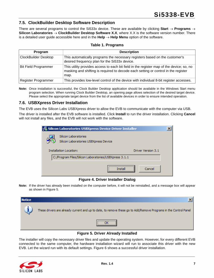
7.6. USBXpress Driver InstallationThe EVB uses the Silicon Labs USBXpress driver to allow the EVB to communicate with the computer via USB.
The driver is installed after the EVB software is installed. Click Install to run the driver installation. Clicking Cancelwill not install any files, and the EVB will not work with the software.
Figure 4. Driver Installer Dialog
Note: If the driver has already been installed on the computer before, it will not be reinstalled, and a message box will appearas shown in Figure 5.
Figure 5. Driver Already Installed
The installer will copy the necessary driver files and update the operating system. However, for every different EVBconnected to the same computer, the hardware installation wizard will run to associate this driver with the newEVB. Let the wizard run with its default settings. Figure 6 shows a successful driver installation.
Table 1. Programs
Program Description
ClockBuilder Desktop This automatically programs the necessary registers based on the customer's desired frequency plan for the Si533x device.
Bit Field Programmer This utility provides access to each bit field in the register map of the device; so, no masking and shifting is required to decode each setting or control in the register map.
Register Programmer This provides low-level control of the device with individual 8-bit register accesses.

Si5338-EVB
8 Rev. 1.4
Figure 6. Successful Driver Installation

Si5338-EVB
Rev. 1.4 9
The USBXpress driver may be removed via the Add and Remove Programs utility in the Control Panel. Locate theentry called Silicon Laboratories USBXpress Device. Click the button, and it should show the version and locationof what it will remove.
Figure 7. Driver Uninstall Location
The USBXpress installation files are located with the ClockBuilder Desktop Software. The driver files for the EVBmay be reinstalled from this location or by running the install software.
Figure 8. Driver Installation Files
Si5338-EVB
10 Rev. 1.4
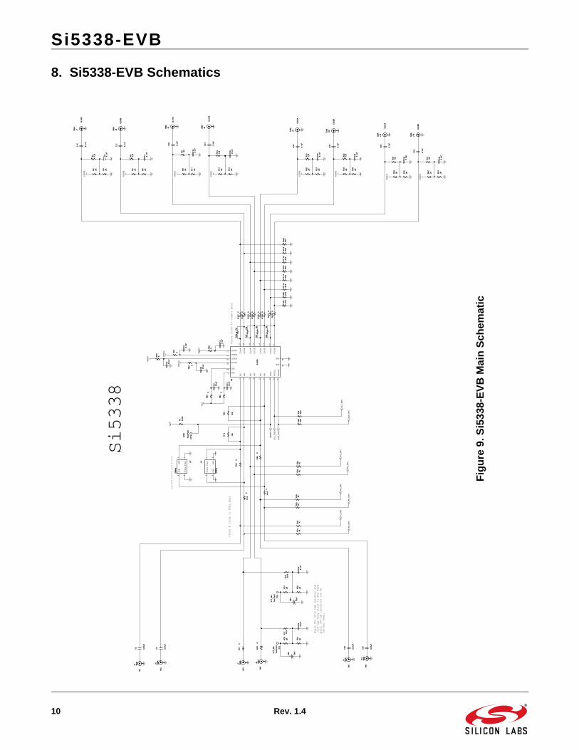
8. Si5338-EVB Schematics
VD
DO
1
VD
DO
3
VD
DO
2
VD
D
VD
DO
0
+3.3
V
VD
DO
0
VD
DO
0
VD
DO
1
VD
DO
1
VD
DO
2
VD
DO
2
VD
DO
3
VD
DO
3
SD
A_5
338
SC
L_53
38
INTR
PT
IN3_
DR
V
IN4_
DR
V
IN5_
DR
V
IN6_
DR
V
IN1_
DR
V
IN2_
DR
V
SC
L_D
RV
SD
A_D
RV
Place the 49.9 ohm resistor and
.1uf cap very close to the 5338
pins. The 2K resistors can be
further away.
Place R close to XTAL pins
Si5338
Dumm
y XT
AL u
sed
for
trac
e ma
tchi
ng
Place close to output pins
J3 SM
A
IN2
J3 SM
A
IN2
R33
2KR33
2K
R25
1KR25
1K
R47
49.9
R47
49.9
C8
0.1u
FC
80.
1uF
R12
20
R12
20
R13
0R
130
C44
0.1u
F
C44
0.1u
F
R83
0R
830
R1
130
R1
130
R40
2KR40
2K
R12
80
R12
80
R26
1KR26
1K
R45
0R
450
R12
0R
120
J8 SM
AIN
4
J8 SM
AIN
4
R32
130
R32
130
C22
0.1u
FC
220.
1uF
R12
70
R12
70
C7
0.1u
FC
70.
1uF
R11
749
.9R
117
49.9
C15
0.1u
F
C15
0.1u
F
C4
0.1u
FC
40.
1uF
R86
100
R86
100
R12
60
R12
60
R84
0R
840
C30
0.1u
FC
300.
1uF
J9SM
A
CLK
2A
J9SM
A
CLK
2A
R20
2KR20
2K R36
2KR36
2K
C5
0.1u
FC
50.
1uF
R88
100
R88
100
R77
0R
770
R12
50
R12
50
R34
2KR34
2K
R12
40
R12
40
C18
0.1u
FC
180.
1uF
R12
30
R12
30
R78
0R
780
C9
0.1u
FC
90.
1uF
J1SM
A
CLK
0A
J1SM
A
CLK
0A
R39
100
R39
100
C41
0.1u
F
C41
0.1u
F
C14
0.1u
FC
140.
1uF
C54
0.1u
F
C54
0.1u
F
R82
0R82
0
R18 49
.9R
18 49.9
R11
649
.9R
116
49.9
R10
100
R10
100
J13
SM
AIN
6
J13
SM
AIN
6
J6SM
A
CLK
1B
J6SM
A
CLK
1B
R19
130
R19
130
R27
2KR27
2K
J2 SM
A
IN1
J2 SM
A
IN1
R8
130
R8
130
R12
049
.9R
120
49.9
R81
0R81
0
R85
100
R85
100
R21
1KR21
1K
J14
SM
A
CLK
3B
J14
SM
A
CLK
3B
R29
49.9
R29
49.9
25M
Hz
U1
25M
Hz
U1
XTAL
11
GN
D2
XTAL
23
GN
D4
25M
Hz
U7
25M
Hz
U7
XTAL
11
GN
D2
XTAL
23
GN
D4
R42
2KR42
2K
C12
0.1u
FC
120.
1uF
R12
10
R12
10
R44
0R
440
J7 SM
A
IN3
J7 SM
A
IN3
R5
2KR5
2K
C11
0.1u
FC
110.
1uF
C28
0.1u
FC
280.
1uF
C40
0.1u
F
C40
0.1u
F
C53
0.1u
F
C53
0.1u
F
R41
130
R41
130
J4SM
A
CLK
0B
J4SM
A
CLK
0B
R30
2KR30
2K
R80
0
R80
0
R15
2KR15
2K
R17 49
.9R
17 49.9
C3
0.01
uF
C3
0.01
uF
+C58
10uF
+C58
10uF
R11
549
.9R
115
49.9
R2
2KR2
2K
C24
0.1u
FC
240.
1uF
R31
2KR31
2K
R87
100
R87
100
J5SM
A
CLK
1A
J5SM
A
CLK
1A
C13
0.1u
FC
130.
1uF
R11
949
.9R
119
49.9
R7
4.99
KR
74.
99K
R28
49.9
R28
49.9
J12
SM
A
CLK
3A
J12
SM
A
CLK
3A
R14
130
R14
130
R9
2KR9
2K
TP1
VTT
_IN
4
Test
Poi
nt
TP1
VTT
_IN
4
Test
Poi
nt
C26
0.01
uF
C26
0.01
uF
R43
2KR43
2K
R6
2KR6
2K
J11
SM
A
IN5
J11
SM
A
IN5
TP2
VTT
_IN
3
Test
Poi
nt
TP2
VTT
_IN
3
Test
Poi
nt
R22
1KR22
1KR
352KR
352K
C17
0.1u
F
C17
0.1u
F
C45
0.1u
F
C45
0.1u
F
C27
0.01
uF
C27
0.01
uF
R79
0R79
0
U2
Si5
338
U2
Si5
338
GND 25
CLK
2A14
IN4
4
IN6
6
IN3
3
IN5
5
IN2
2
IN1
1
CLK
1B17
CLK
1A18
CLK
0B21
CLK
0A22
VDD24
VDDO020
VDDO116
VDDO215
VDDO311
VDD7
INTR
8
IN7/
SCL
12
IN8/
SDA
19
GND 23
CLK
3B9
CLK
3A10
CLK
2B13
R3
2KR3
2K
C20
0.1u
FC
200.
1uF
R16
2KR16
2K
R23
1KR23
1K
R4
130
R4
130
R37
130
R37
130
+C93
10uF
+C93
10uF
R95
49.9
R95
49.9
TP12IN
TR
Test
Poi
nt
TP12IN
TR
Test
Poi
nt
R38
2KR38
2K
R11
2KR11
2K
R11
849
.9R
118
49.9
C23
0.1u
FC
230.
1uF
C2
0.01
uF
C2
0.01
uF
R24
1KR24
1K
J10
SM
A
CLK
2B
J10
SM
A
CLK
2B
Fig
ure
9.S
i533
8-E
VB
Mai
n S
chem
atic

Si5338-EVB
Rev. 1.4 11
IN3_
DR
IVE
IN4_
DR
IVE
SCL_
5338
_DR
V
SDA_
5338
_DR
V
IN1_
DR
IVE
IN1_
DR
IVE
IN2_
DR
IVE
IN2_
DR
IVE
IN5_
DR
IVE
IN6_
DR
IVE
SCL_
5338
_DR
VSD
A_53
38_D
RV
IN6_
EN
IN6_
DR
IVE
IN5_
EN
IN5_
DR
IVE
IN1_
EN
IN2_
EN
I2C
_5V_
ENIN
2_EN
IN5_
ENIN
6_EN
I2C
_5V_
EN
IN1_
EN
IN3_
DR
IVE
IN4_
DR
IVE
+5V_
USB
VDD
+3.3
V
VDD
O1
VDD
O2
VDD
O3
+3.3
V
+3.3
V
+3.3
V
+3.3
V
+3.3
V
VDD
O0
+5V_
USB
+5V_
USB
+5V_
USB
+5V_
USB
+5V_
USB
+5V_
USB
+5V_
USB
+3.3
V +3.3
V+3
.3V
+3.3
V+3
.3V
+5V_
USB
+3.3
V
+3.3
V
+3.3
V
+3.3
V
+3.3
V
+3.3
V
+3.3
V
+3.3
V
+5V_
USB
+3.3
V
+5V_
USB
VDD
_pin
VDD
O1_
pin
VDD
O2_
pin
VDD
O3_
pin
VDD
O0_
pin
IN1_
DR
V
SCL_
5V
SDA_
5V
INTR
PT
SCL_
5V
SDA_
5V
SCL_
5338
SDA_
5338
IN2_
DR
V
IN3_
DR
V
IN4_
DR
V
IN5_
DR
V
IN6_
DR
V
SCL_
DR
V
SDA_
DR
V
SCL_
5V
SDA_
5V
Address is 1001100
MCU
0.9V to 5.5V
2.7V to 5.5V
CLKIN
CLKINB
CMOS
CMOSFB
FBCLK
FBCLKB
SCL
SDA
+1.2V
+1.2V
+1.2V
+1.2V
+2.5V Ref
Address is 1001101
C47
0.1u
F
C47
0.1u
F
J16
J16
12
R63
1.02
KR
631.
02K
D1 M
MBD
3004
S-7-
FD
1 MM
BD30
04S-
7-F
C51
0.1u
F
C51
0.1u
F
C49
0.1u
F
C49
0.1u
F
R96
0R96
0
R97
825
R97
825
J19
HEA
DER
2x2
J19
HEA
DER
2x2
11
33
22
44
D4
Gre
enU
SBD
4G
reen
USB
R50
1KR50
1K
R10
351
1R
103
511
R61
1KR61
1K
R55
2KR55
2KJ1
8J1
81
2
J20
J20
12
C42
0.1u
F
C42
0.1u
FC
43
0.1u
F
C43
0.1u
F
R54
2KR54
2K
NLS
V1T2
44
U5
NLS
V1T2
44
U5
VCCA1
A2
GND 3
B5
OE
B4
VCCB6
+C48
10uF
+C48
10uF
C50
0.1u
F
C50
0.1u
F
C55
0.1u
F
C55
0.1u
F
ADG
728U13
ADG
728U13
SD
A3
RE
SE
TB2
S1
4
S2
5
S3
6
S4
7
D8
A0
16
S8
9
S7
10
S6
11
S5
12
VDD13 GND 14
SC
L1
A1
15
R60
1KR60
1K
R49
1.02
KR
491.
02K
C34
1uF
C34
1uF
R46
1.02
KR
461.
02K
J17
J17
12
C38
0.1u
F
C38
0.1u
F
C56
0.1u
FC
560.
1uF
R69
220
R69
220
J23
CO
NN
SO
CKE
T 5x
2 Sh
roud
ed
J23
CO
NN
SO
CKE
T 5x
2 Sh
roud
ed
11
22
33
44
55
66
77
88
99
1010
S1 SW P
USH
BUTT
ON
S1 SW P
USH
BUTT
ON
R67
220
R67
220
C35
0.1u
F
C35
0.1u
F
R52
2KR52
2K
C59
1uF
C59
1uF
R53
2KR53
2K
R62
1KR
621K
C52
1uF
C52
1uF
D2 M
MBD
3004
S-7-
FD
2 MM
BD30
04S-
7-F
R76
1KR76
1K
U8
C80
51F3
40
U8
C80
51F3
40
VDD10
REGIN11 GND 7
VBUS12
D+
8D
-9
P0.
06
P0.
15
P0.
24
P0.
33
P0.
42
P0.
51
P0.
648
P0.
747
P1.
046
P1.
145
P1.
244
P1.
343
P1.
442
P1.
541
P1.
640
P1.
739
P2.
038
P2.
137
P2.
236
P2.
335
P2.
434
P2.
533
P2.
632
P2.
731
P3.
030
P3.
129
P3.
228
P3.
327
P3.
426
P3.
525
P3.
624
P3.
723
P4.
022
P4.
121
P4.
220
P4.
319
P4.
418
P4.
517
P4.
616
P4.
715
RS
T/C
2CK
13C
2D14
J22
J22
12
R10
151
1R
101
511
C37
0.1u
FC
370.
1uF
R99
511
R99
511
D5
Gre
enI2
CD
5G
reen
I2C
NLS
V1T2
44
U10
NLS
V1T2
44
U10
VCCA1
A2
GND 3
B5
OE
B4
VCCB6
J21
USB
Typ
e B
J21
USB
Typ
e B
1 2 3 4
56
C57
0.1u
FC
570.
1uF
J25
J25
12
C31
0.1u
F
C31
0.1u
F
R66
412
R66
412
D3
Red
INTR
D3
Red
INTR
+C87
10uF
+C87
10uF
R98
511
R98
511
C32
0.1u
F
C32
0.1u
F
R11
00R
110
0
TP11
GN
DTe
st P
oint
TP11
GN
DTe
st P
oint
TP3
SDA
Test
Poi
ntTP
3
SDA
Test
Poi
nt
NLS
V1T2
44
U3
NLS
V1T2
44
U3
VCCA1
A2
GND 3
B5
OE
B4
VCCB6
C36
0.1u
F
C36
0.1u
F
C46
0.1u
F
C46
0.1u
F
PCA9
517A
U6
PCA9
517A
U6
VC
CA
1
SC
LA2
SD
AA
3
GN
D4
VC
CB
8
SC
LB7
EN
5
SD
AB
6
R64
1.02
KR
641.
02K
NLS
V1T2
44
U11
NLS
V1T2
44
U11
VCCA1
A2
GND 3
B5
OE
B4
VCCB6
ADG
728U14
ADG
728U14
SD
A3
RE
SE
TB2
S1
4
S2
5
S3
6
S4
7
D8
A0
16
S8
9
S7
10
S6
11
S5
12
VDD13 GND 14
SC
L1
A1
15
R65
1KR
651K
J15
J15
12
C33
4.7u
FC
334.
7uF
D6
Gre
enR
DY
D6
Gre
enR
DY
R68
220
R68
220
R11
10R
111
0
2.5V
U4
2.5V
U4
VO
UT
1
GND 2
VIN
3
TP4
SCL
Test
Poi
ntTP
4
SCL
Test
Poi
nt
J24
J24
12
C39
0.1u
F
C39
0.1u
F
R10
2 825
R10
2 825
R10
4 825
R10
4 825
R10
0 825
R10
0 825
R51
1KR51
1K
Fig
ure
10.S
i533
8-E
VB
MC
U S
chem
atic

Si5338-EVB
12 Rev. 1.4
VDD
O1_
int_
en
VDD
O0_
int_
en
VDD
O3_
int_
en
VDD
O2_
int_
en
VDD
_int
_en
VDD
_int
_en
VDD
O3_
int_
en
VDD
O2_
int_
en
VDD
O1_
int_
en
VDD
O0_
int_
en
+5V_
USB
+5V_
USB
+5V_
USB
+5V_
USB
+5V_
USB
+5V_
USB
+5V_
USB
+5V_
USB
+5V_
USB
+5V_
USB
+5V_
USB
+5V_
USB
+5V_
USB
+5V_
USB
+5V_
USB
+5V_
USB
+5V_
USB
VDD
VDD
O0
VDD
O1
VDD
O2
VDD
O3
+3.3
V
VDD
O0_
pin
VDD
O1_
pin
VDD
O2_
pin
VDD
O3_
pin
VDD
_pin
SDA_
5V
SCL_
5V
SDA_
5V
SCL_
5V
SDA_
5V
SCL_
5V
Address is 0101100
Address is 0101101
Address is 0101110
Voltage
Regulators
C84
0.1u
FC
840.
1uF
J28
JUM
PER
J28
JUM
PER
12
C83
0.01
uFC
830.
01uF
R73
10K
R73
10K
U17
MAX
8869
U17
MAX
8869
GN
D
10
IN4
OU
T12
RS
TB6
SE
T
11
SH
DN
B7
IN5
IN3
IN2
OU
T13
OU
T14
OU
T15
SS
8
NC16
NC9
NC1
EP
AD
17
C66
1uF
C66
1uF
+C63 10
uF
+C63 10
uF
J27
JUM
PER
J27
JUM
PER
12
R10
510
R10
510
U21
MAX
8869
U21
MAX
8869
GN
D
10
IN4
OU
T12
RS
TB6
SE
T
11
SH
DN
B7
IN5
IN3
IN2
OU
T13
OU
T14
OU
T15
SS
8
NC16
NC9
NC1
EP
AD
17
R74
47.5
K
R74
47.5
K
TP8
VDD
O3
Test
Poi
ntTP
8
VDD
O3
Test
Poi
nt
R71
10K
R71
10K
C69 1uF
C69 1uF
TP17
GN
DTe
st P
oint
TP17
GN
DTe
st P
oint
J29
JUM
PER
J29
JUM
PER
12
C75
0.01
uFC
750.
01uF
C91
1uF
C91
1uF
C62
1uF
C62
1uF
U16
MAX
8869
U16
MAX
8869
GN
D
10
IN4
OU
T12
RS
TB6
SE
T
11
SH
DN
B7
IN5
IN3
IN2
OU
T13
OU
T14
OU
T15
SS
8
NC16
NC9
NC1
EP
AD
17
C64
1uF
C64
1uF U
20
AD52
63
U20
AD52
63
GND 8
W4
19
A4
20
B3
4
W3
6
W1
3
A3
5
A1
2
B1
1
B4
21
W2
22
A2
23
B2
24
NC
/O2
17
SD
O/O
116
VLOGIC10
CS
B/A
D0
13R
ES
B/A
D1
14
SH
DN
_B15
VDD7
DIS
9
SD
I/SD
A11
CLK
/SC
L12
VSS 18
C73 1uF
C73 1uF
TP16
GN
DTe
st P
oint
TP16
GN
DTe
st P
oint
U22
MAX
8869
U22
MAX
8869
GN
D
10
IN4
OU
T12
RS
TB6
SE
T
11
SH
DN
B7
IN5
IN3
IN2
OU
T13
OU
T14
OU
T15
SS
8
NC16
NC9
NC1
EP
AD
17
+C61 10
uF
+C61 10
uF
C60
1uF
C60
1uF
R10
610
R10
610
+C67 10
uF
+C67 10
uF
C81
1uF
C81
1uF
TP15
GN
DTe
st P
oint
TP15
GN
DTe
st P
oint
R72
10K
R72
10K
U18
MAX
8869
U18
MAX
8869
GN
D
10
IN4
OU
T12
RS
TB6
SE
T
11
SH
DN
B7
IN5
IN3
IN2
OU
T13
OU
T14
OU
T15
SS
8
NC16
NC9
NC1
EP
AD
17
U23
AD52
63
U23
AD52
63
GND 8
W4
19
A4
20
B3
4
W3
6
W1
3
A3
5
A1
2
B1
1
B4
21
W2
22
A2
23
B2
24
NC
/O2
17
SD
O/O
116
VLOGIC10
CS
B/A
D0
13R
ES
B/A
D1
14
SH
DN
_B15
VDD7
DIS
9
SD
I/SD
A11
CLK
/SC
L12
VSS 18
C80 1uF
C80 1uF
C89
1uF
C89
1uF
R10
910
R10
910
TP13
VDD
Test
Poi
ntTP
13
VDD
Test
Poi
nt
C68 1uF
C68 1uF
TP14
GN
DTe
st P
oint
TP14
GN
DTe
st P
oint
C88
1uF
C88
1uF
C78
1uF
C78
1uF
C72
0.01
uFC
720.
01uF
C90
1uF
C90
1uF
R75
15.4
KR
7515
.4K
C71
0.01
uF
C71
0.01
uF
U15
MAX
8869
U15
MAX
8869
GN
D
10
IN4
OU
T12
RS
TB6
SE
T
11
SH
DN
B7
IN5
IN3
IN2
OU
T13
OU
T14
OU
T15
SS
8
NC16
NC9
NC1
EP
AD
17
C85 1uF
C85 1uF
TP5
VDD
O0
Test
Poi
ntTP
5
VDD
O0
Test
Poi
nt
C86
0.01
uFC
860.
01uF
+C65 10
uF
+C65 10
uF
J26
JUM
PER
J26
JUM
PER
12
C76
0.01
uFC
760.
01uF
TP6
VDD
O1
Test
Poi
ntTP
6
VDD
O1
Test
Poi
nt
+C79 10
uF
+C79 10
uF
J30
JUM
PER
J30
JUM
PER
12
TP7
VDD
O2
Test
Poi
ntTP
7
VDD
O2
Test
Poi
nt
+C82
10uF
+C82
10uF
C74
0.1u
FC
740.
1uF
C70 1uF
C70 1uF
C77
0.1u
FC
770.
1uF
C92
1uF
C92
1uF
R70
10K
R70
10K
U19
AD52
63
U19
AD52
63
GND 8
W4
19
A4
20
B3
4
W3
6
W1
3
A3
5
A1
2
B1
1
B4
21
W2
22
A2
23
B2
24
NC
/O2
17
SD
O/O
116
VLOGIC10C
SB
/AD
013
RE
SB
/AD
114
SH
DN
_B15
VDD7
DIS
9
SD
I/SD
A11
CLK
/SC
L12
VSS 18
R10
710
R10
710
R10
810
R10
810
TP10
+3.3
VTe
st P
oint
TP10
+3.3
VTe
st P
oint
Fig
ure
11.S
i533
8-E
VB
Vo
ltag
e R
egu
lati
on
Sch
emat
ic

Si5338-EVB
Rev. 1.4 13
9. Bill of Materials
Table 2. Si5338-EVB Bill of Materials
Item NI Qty Reference Value Manufacturer Part Number
1 10 C2,C3,C26,C27,C71,C72, C75,C76,C83,C86
0.01 µF Venkel C0402X7R100-103M
2 35 C15,C17,C31,C32,C35,C36,C37,C38,C39,C40,C41,C42,C43,C44,C45,C46,C47,C49,C50,C51,C53,C54,C55,C56,C57,C74,C77,C84,C5,C8,C9,C11,C12
0.1 µF Venkel C0402X7R100-104K
C13
4 1 C33 4.7 µF Venkel C1206X7R100-475M
5 3 C34,C52,C59 1 µF Venkel C1206X7R250-105K
6 7 C48,C61,C63,C65,C67, 10 µF Kemet B45196H5106M309
C79,C82
7 17 C60,C62,C64,C66,C68,C69, 1 µF Venkel C0603X7R100-105K
C70,C73,C78,C80,C81,C85,
C88,C89,C90,C91,C92
8 2 D1,D2 MMBD3004S-7-F Diodes Inc. MMBD3004S-7-F
9 1 D3 Red Panasonic LN1271RAL
10 3 D4,D5,D6 Green Panasonic LN1371G
11 14 J1,J2,J3,J4,J5,J6,J7,J8, SMA Johnson Components
142-0701-801
J9,J10,J11,J12,J13,J14
12 13 J15,J16,J17,J18,J20,J22, JUMPER Samtec TSW-102-07-T-S
J24,J25,J26,J27,J28,J29,J30
13 1 J19 HEADER 2x2 Samtec TSW-102-07-T-D
14 1 J21 USB Type B Tyco 292304-1
15 1 J23 CONN SOCKET 5x2 Shrouded
Tyco 5103309-1
18 1 R7 4.99K Venkel CR0402-16W-4991F
19 1 R39 100 Venkel CR0201-20W-1000F
20 7 R44,R45,R77,R78,R96,R110,R111
0 Venkel CR0402-16W-000
21 2 R28,R29 49.9 Venkel CR0402-16W-49R9F
22 13 R21,R22,R23,R24,R25,R26, 1K Venkel CR0402-16W-102J
R50,R51,R60,R61,R62,R65,R76
23 4 R46,R49,R63,R64 1.02K Venkel TFCR0402-16W-E-1021B
25 4 R52,R53,R54,R55 2K Venkel CR0402-16W-2001F
26 1 R66 412 Venkel TFCR0402-16W-E-4120B
27 3 R67,R68,R69 220 Venkel CR0402-16W-221J
28 4 R70,R71,R72,R73 10K Venkel CR0402-16W-103J
29 1 R74 47.5K Venkel CR0603-10W-4752F
30 1 R75 15.4K Venkel CR0603-10W-1542F
31 6 R79,R80,R81,R82,R83,R84 0 Venkel CR0603-16W-000

Si5338-EVB
14 Rev. 1.4
32 4 R97,R100,R102,R104 825 Venkel CR0603-10W-8250F
33 4 R98,R99,R101,R103 511 Venkel CR0603-10W-5110F
34 5 R105,R106,R107,R108,R109 10 Venkel CR2512-2W-10R0D
35 8 R121,R122,R123,R124,R125,R126,R127,R128
0 Venkel CR0201-20W-000F
36 1 S1 SW PUSHBUTTON Mountain Switch 101-0161-EV
37 1 TP11 Test Point Kobiconn 151-207
38 1 U1 25 MHz Epson FA-238 25.0000MB
39 1 U2 Si5338 SiLabs Si5338N-A-GMR
40 4 U3,U5,U10,U11 NLSV1T244 On Semi NLSV1T244MUTBG
41 1 U4 2.5 V Analog Devices AD1582BRT
42 1 U6 PCA9517A NXP PCA9517AD
43 1 U8 C8051F340 SiLabs C8051F340-GQ
44 2 U13,U14 ADG728 Analog Devices ADG728BRUZ
45 6 U15,U16,U17,U18,U21,U22 MAX8869 MAXIM MAX8869EUE50
46 3 U19,U20,U23 AD5263 Analog Devices AD5263BRUZ20
47 4 Standoffs SPC Technology 2397
48 4 Screws Richco NSS-4-4-01
49 7 Jumpers Sullins SPC02SYAN
Do Not Populate
2 NI 9 C4,C7,C14,C18, 0.1 µF Venkel C0402X7R100-104K
C22,C23,C20, C24,C28,C30,
6 NI 3 C58, C93, C87 10 µF Kemet B45196H5106M309
16 NI 8 R1,R4,R8,R14,R19,R32,R37, 130 Venkel CR0402-16W-131F
R41
17 NI 20 R2,R3,R5,R6,R9,R11,R15, 2K Venkel TFCR0402-16W-E-2001B
R16,R20,R27,R30,R31,R33,
R34,R35,R36,R38,R40,R42,
R43
19 NI 5 R10,R85,R86,R87,R88 100 Venkel CR0201-20W-1000F
20 NI 2 R12,R13 0 Venkel CR0402-16W-000
24 NI 8 R47,R95,R115,R116,R117, 49.9 Venkel CR0402-16W-49R9F
R118,R119,R120
21 NI 2 R17,R18 49.9 Venkel CR0402-16W-49R9F
37 NI 12 TP1,TP2,TP3,TP4,TP5,TP6, Test Point Kobiconn 151-207
TP7,TP8,TP9,TP10,TP12,TP13
38 NI 1 U7 25 MHz Epson FA-238 25.0000MB-W
Table 2. Si5338-EVB Bill of Materials (Continued)
Item NI Qty Reference Value Manufacturer Part Number

Si5338-EVB
Rev. 1.4 15
DOCUMENT CHANGE LIST
Revision 0.1 to Revision 1.0Replaced the voltage input terminal block with
programmable regulators.
The board is entirely powered from USB power.
Added an additional LED to indicate MCU ready.
Added jumpers on all input pins to allow external control of features, such as output enable, and frequency and phase increment and decrement.
Revision 1.0 to Revision 1.1Changed “Si533x configuration” to “Any Rate
Clock Generator” throughout.
Changed “Si5338 Programmer” to “MultiSynth Clock Programmer” throughout.
Updated Table 1, “Programs,” on page 7.
Updated Figures 3, 4, and 8.
Revision 1.1 to Revision 1.2Changed “Any Rate Clock Generator” to
“ClockBuilder Desktop” throughout.
Changed “MultiSynth Clock Programmer” to “ClockBuilder Desktop” throughout.
Updated Figure 3 on page 6.
Removed “Uninstaller Option” figure.
Updated Figure 8 on page 9.
Revision 1.2 to Revision 1.3Added "9. Bill of Materials" on page 13.
Revision 1.3 to Revision 1.4Added "6.1. Evaluating LVPECL Output Clocks"
on page 5.
Added references to the Si5335.

DisclaimerSilicon Laboratories intends to provide customers with the latest, accurate, and in-depth documentation of all peripherals and modules available for system and software implementers using or intending to use the Silicon Laboratories products. Characterization data, available modules and peripherals, memory sizes and memory addresses refer to each specific device, and "Typical" parameters provided can and do vary in different applications. Application examples described herein are for illustrative purposes only. Silicon Laboratories reserves the right to make changes without further notice and limitation to product information, specifications, and descriptions herein, and does not give warranties as to the accuracy or completeness of the included information. Silicon Laboratories shall have no liability for the consequences of use of the information supplied herein. This document does not imply or express copyright licenses granted hereunder to design or fabricate any integrated circuits. The products must not be used within any Life Support System without the specific written consent of Silicon Laboratories. A "Life Support System" is any product or system intended to support or sustain life and/or health, which, if it fails, can be reasonably expected to result in significant personal injury or death. Silicon Laboratories products are generally not intended for military applications. Silicon Laboratories products shall under no circumstances be used in weapons of mass destruction including (but not limited to) nuclear, biological or chemical weapons, or missiles capable of delivering such weapons.
Trademark InformationSilicon Laboratories Inc., Silicon Laboratories, Silicon Labs, SiLabs and the Silicon Labs logo, CMEMS®, EFM, EFM32, EFR, Energy Micro, Energy Micro logo and combinations thereof, "the world’s most energy friendly microcontrollers", Ember®, EZLink®, EZMac®, EZRadio®, EZRadioPRO®, DSPLL®, ISOmodem ®, Precision32®, ProSLIC®, SiPHY®, USBXpress® and others are trademarks or registered trademarks of Silicon Laboratories Inc. ARM, CORTEX, Cortex-M3 and THUMB are trademarks or registered trademarks of ARM Holdings. Keil is a registered trademark of ARM Limited. All other products or brand names mentioned herein are trademarks of their respective holders.
http://www.silabs.com
Silicon Laboratories Inc.400 West Cesar ChavezAustin, TX 78701USA
ClockBuilder Pro
One-click access to Timing tools, documentation, software, source code libraries & more. Available for Windows and iOS (CBGo only).
www.silabs.com/CBPro
Timing Portfoliowww.silabs.com/timing
SW/HWwww.silabs.com/CBPro
Qualitywww.silabs.com/quality
Support and Communitycommunity.silabs.com