using one circuit to control another: transistor basics jeff bourne northview … · 2018-04-19 ·...
TRANSCRIPT

Using one circuit to control another: Transistor basics
Jeff Bourne
Northview High School
Fulton County Public Schools
Problem: How can one circuit that may have a small current control another circuit that may have a much greater
current?
Abstract: Students will attempt to control a LED circuit attached to a nine volt battery by utilizing PNP or NPN
bipolar transistor circuits as well as a FET. Basic diode theory and forward and reverse bias will be explored in
the laboratory setting as well. Students will build circuits using different types of transistors. The unit ends
with students re-examining the triboelectric series using a FET to determine type of charge.
National and State Standards
2. State of Georgia Standards: Characteristics of Science
SCSh1. Students will evaluate the importance of curiosity, honesty, openness, and skepticism in science.
c. Explain the further understanding of scientific problems relies on the design and execution of
new experiments which may reinforce or weaken opposing explanations.
SCSh3. Students will identify and investigate problems scientifically.
b. Develop procedures for solving scientific problems.
c. Collect, organize and record appropriate data.
d. Graphically compare and analyze data points and /or summary statistics
e. Develop reasonable conclusions based on data collected.
f. Evaluate whether conclusions are reasonable by reviewing the process and checking against
other available information.
SCSh4. Students will use tools and instruments for observing, measuring, and manipulating scientific
equipment and materials.
a. Develop and use systematic procedures for recording and organizing information.
b. Use technology to produce tables and graphs
SCSh6. Students will communicate scientific investigations and information clearly.
a. Write clear, coherent laboratory reports related to scientific investigations.
SP5. Students will evaluate relationships between electrical and magnetic forces.
a. describe the transformation of mechanical energy into electrical energy and the transmission of
electrical energy.

b. determine the relationship among potential difference, current, and resistance in a dc circuit.
Prior Knowledge of Students coming into this activity: (The assumption is that this unit is intended for AP Physics B
students following the National exam.)
1. Students will understand the basics of electrostatics, charge, electric potential, resistance, and current.
2. Students will know how to assemble simple series and parallel circuits on a standard breadboard.
3. Students will be familiar with the DMM and be able to use it to measure voltage, current, or resistance.
Objectives:
1. Students will be able to describe the differences between conductors, insulators, and semiconductors in
terms of valence and conductive bands.
2. Understand the mechanics of a diode, and how it is forward or reversed biased.
3. Understand the basic principles and function of a bipolar transistor
4. Understand the basic principles and function of a field effect transistor
Anticipated learner outcomes
Conceptual:
1. Understand how band theory explains the different properties of conductors, insulators, and
semiconductors.
2. Understand the concept of one circuit controlling another
3. Describe in basic terms the purpose and function of both NPN and PNP bipolar transistors.
4. Describe how a FET works.
Experimental:
1. Build a simple LED circuit on a breadboard.
2. Run diagnostics on diodes and transistors with the DMM.
3. Correctly wire a LED circuit on a breadboard that uses either a PNP or NPN bipolar transistor to turn the LED
on and off.
4. Build a simple electrometer using a FET and use it to verify the triboelectric series.
Background information
Conductors, insulators, and semiconductors
Students coming out of general high school chemistry have been briefly exposed to the ideas of quantum
energy levels for electrons in atoms. It is probable that valence electrons and Pauli’s Exclusion Principle were
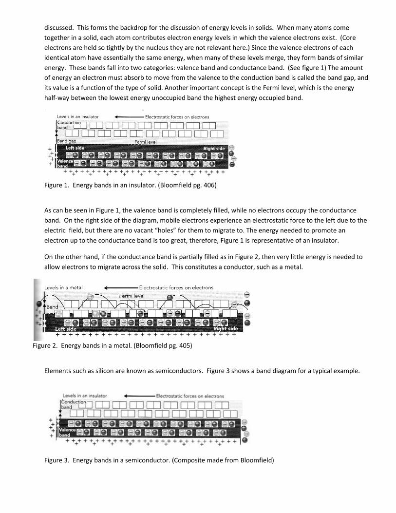
discussed. This forms the backdrop for the discussion of energy levels in solids. When many atoms come
together in a solid, each atom contributes electron energy levels in which the valence electrons exist. (Core
electrons are held so tightly by the nucleus they are not relevant here.) Since the valence electrons of each
identical atom have essentially the same energy, when many of these levels merge, they form bands of similar
energy. These bands fall into two categories: valence band and conductance band. (See figure 1) The amount
of energy an electron must absorb to move from the valence to the conduction band is called the band gap, and
its value is a function of the type of solid. Another important concept is the Fermi level, which is the energy
half-way between the lowest energy unoccupied band the highest energy occupied band.
Figure 1. Energy bands in an insulator. (Bloomfield pg. 406)
As can be seen in Figure 1, the valence band is completely filled, while no electrons occupy the conductance
band. On the right side of the diagram, mobile electrons experience an electrostatic force to the left due to the
electric field, but there are no vacant “holes” for them to migrate to. The energy needed to promote an
electron up to the conductance band is too great, therefore, Figure 1 is representative of an insulator.
On the other hand, if the conductance band is partially filled as in Figure 2, then very little energy is needed to
allow electrons to migrate across the solid. This constitutes a conductor, such as a metal.
Figure 2. Energy bands in a metal. (Bloomfield pg. 405)
Elements such as silicon are known as semiconductors. Figure 3 shows a band diagram for a typical example.
Figure 3. Energy bands in a semiconductor. (Composite made from Bloomfield)

The obvious difference between a semiconductor and an insulator is that the band gap for the semiconductor is
much smaller, allowing for the possibility of electron promotion due to thermal energy. For this reason, the
conductance of a material such as pure silicon improves with increases in temperature. However, the number
of charge carriers in a pure semiconductor is very small, meaning that silicon has limited use in electrical
applications.
To improve the conductance of silicon (or another tetravalent semiconductor such as germanium), atoms with
different number of valence electrons are introduced into the atomic matrix. These atoms are referred to as
dopants, and the semiconductor is said to have been “doped”. If an atom such as Gallium or Indium with 3
valence electrons is added, it creates “holes” in the valence bands. These are called p-type semiconductors
because of the positive holes established throughout the solid. (See Figure 4a) If instead, an impurity such as
Arsenic with 5 valence electrons is added to the silicon, the “extra” electron goes into the conductance band as
shown in Figure 4b. These are referred to as N-type semiconductors because of the abundance of negative
electrons. Under the influence of an external electric field, it is now much easier for electrons to move across
the solid since the energy necessary is much smaller as can be seen in the diagrams.
Figure 4a P-type semiconductor Figure 4b N-type semiconductor
(Bloomfield page 408) Diodes
A diode is formed when a p-type and n-type semiconductor are brought together in what is known as a p-n
junction. As seen in Figure 5, conductance electrons from the n-type quickly fall into the holes of the p-type.
This current is short-lived, however, because this electron movement produces actual positive and negative
environments, establishing a capacitor-like region at the junction, preventing further migration of electrons
against the electric field. Thus, a depletion zone is created at the junction.
Figure 5. p-n junction (Bloomfield pg. 408)

It is this depletion region that gives diodes their very unique property: they only allow current to flow in one
direction, and not the other. If a wire from the positive terminal of the battery is attached to the p side, and
the n side is connected to the negative terminal, then the electric force from the field adds electrons to the n
side and removes electrons from the p side, effectively removing the depletion zone, allowing for current to
flow. The diode is said to be “forward-biased” (Figure 6a). The threshold voltage for a silicon-based diode is 0.6
V, meaning that under that voltage the depletion zone continues to prevent current. If the wires are reversed,
and now the n side is connected to a negative voltage, then the electric force actually widens the depletion
zone, preventing current to flow in that direction; the diode is reversed biased. (Figure 6b) In schematic
drawings, diodes are presented by Figure 7a.
Figure 7a Diodes electronicdesignworks.com
Figure 6 Forward and Reversed Bias across a pn junction. (Bloomfield pg. 409)
Figure 7b LED schematic
In the typical silicon diode, when the electrons fall from the conductance band into holes in the valence band, that
energy is released in the form of an infrared photon. However, if the diode is composed of other atoms such as
GaAsxP1-x, then the energy gap becomes large enough that photons in the visible spectrum are emitted instead.
These diodes are known as Light Emitting Diodes (LED). The specific color of an LED depends on what types of
atoms and their concentrations in the diode. Figure 7b is the schematic for a LED. In wiring a LED into a circuit, the
longer arm always has the more positive potential.
Transistors
Transistors are semiconducting devices that allow for control of current between circuits. In that sense, they share
a similar function as the electromagnetic relay previously discussed in a typical physics class. In fact, the transistor
replaced the relay in many applications, which paved the way for much smaller and faster devices. For purposes of
this lesson plan, it is not necessary to go into great detail about all types of transistors and integrated circuits, but
will instead focus on the basic bipolar transistor and the Field Effect Transistor (FET).
A bipolar transistor is essentially two diodes put together, producing two junctions. Combinations include the NPN
and PNP transistors. Typically, the outside regions are more heavily doped and much wider than the middle region.
The regions are called the collector, base, and emitter. (Figure 8)

Figure 8. Bipolar transistor composition thefullwiki.org
The basic principle of the transistor that I want students to understand is that the base acts like a switch, which
turns current on and off through the collector and emitter. The base is like a faucet controlling large amounts of
water flowing through large pipes. In a bipolar transistor, a very small current passing between the base and
emitter allows for a much larger (can be more than 100 times) current gain to flow between the collector and
emitter. This illustrates the amplifier function of the transistor.
The key concept I want students to grasp is that it is vital that the base-emitter junction become forward biased.
When that happens, then resistance between the collector and emitter essentially disappears and current flows. In
the NPN transistor, that requires the base to have a positive voltage compared to the emitter. The reverse is true
for the PNP transistor: the emitter voltage must be more positive than the base. This arrangement will be
confirmed in the lab.
In order for students to build circuits involving bipolar transistors, they must recognize both the schematic
representations as well as the actual component. Figure 9 shows both. In the schematics, it is important to
remember that the arrow points in the direction of conventional current. It is also critical that the current through
the base be kept low enough to protect the transistor, therefore, the base will always have a resistor connected in
series with it.
Figure 9a Transistor schematic kpsec.freeuk.com Figure 9b Actual bipolar transistor reuk.co.uk
A field effect transistor (FET) does not actually require a current to travel through the base to the emitter. All that
matters is that an electric field be established at the base circuit, which causes the resistance between the collector
and emitter to drop. With FET’s, it is much more common to use the terms gate, source, and drain. Figure 10
illustrates the principle of a basic FET.
Figure 10. Principles of FET operation. Bloomfield

In this case, since there is a dielectric material (often SiO2) separating the gate from the rest of the transistor, it is
referred to as a Metal Oxide Semiconductor Field Effect Transistor (MOSFET). The figure on the left is a N-channel
MOSFET that is off. The depletion region between the source and drain is rich in positive holes, which prevents
electrons to flow. When the gate experiences a positive charge, an electric field is established which pulls in
electrons from the surrounding materials. The holes are filled, and the depletion region has now become similar to
the source and drain, allowing current to flow. An extremely useful feature is that the current can be controlled
precisely by the size of the electric field. Just as there are two types of bipolar transistors, there are also N-channel
and P-channel MOSFET’s. In order for a P-channel MOSFET to become conductive, the gate should have a negative
potential. Figure 11 is the schematic for a FET.
Figure 11 FET schematic. Dystompboxes.com
The thickness of the dielectric material is a critical feature of the MOSFET; it needs to be as thin as possible to
increase capacitance, but not so thin that large voltages cause a breakdown spark to discharge the capacitor. (This
is one reason why static electricity is so dangerous for electrical devices.) For this reason, other materials with
higher dielectric constants such as alumina and titanium oxides are being used more and more. The higher the
dielectric constant, the thicker the layer can be and still maintain similar capacitance. For example, since the
dielectric constant of SiO2 is about 4, a material with a dielectric constant of 20 (like HfO2) could be five times
thicker!
Materials and Supplies
Breadboards with connecting wires
Power supply Batteries (9 and 1.5 V)
wires NPN transistors PN2222
PNP transistors PN2905
Assorted Resistors: 470 Ω, 1K, 10K, 100K
LED’s CdS photoresistors DMM
Diodes Switches FET’s
Plan
Day 1: Introduction of the unit. I will talk to the students about the field of electronics and electrical engineering.
As a demonstration, I will have a breadboard with this circuit wired in:
The two LEDs are blinking back and forth. The concept I want to discuss with them is the
fact that there are two circuits interacting with each other. I will remind students that
we’ve already studied relays, but this circuit uses a different device called a transistor.
There are several goals for this unit.
1. To gain some basic understanding of diodes and transistors;
2. To learn how to wire LED’s, capacitors, resistors, and transistors in circuits

3. To design and build a simple circuit that monitors something, such as water level, or moisture content.
4. To have FUN and possibly stir up some thoughts about electrical engineering.
The background information will be presented to the students. A handout with appropriate pictures and diagrams
will be given to each student to follow along, or a Powerpoint could be produced.
Day 2: Each student group will receive the lab equipment and lab handout.
Goals for today:
1. Use the DMM to assess the + and – end of a diode.
2. Use the DMM to determine the + and – end of a LED
3. Use the DMM to determine how the resistance changes in a CdS photoresistor depending on the light
4. Use the DMM to determine the collector, gate, and emitter connections on the transistors
Day 3: Each student group will receive the lab equipment and lab handout.
Goals for today: (May carry over to tomorrow.)
1. Wire a basic NPN transistor circuit and LED. Make all VIR measurements.
2. Wire a basic PNP transistor circuit and LED. Make all VIR measurements.
3. Wire a basic NPN transistor circuit that incorporates the CdS photoresistor. The LED should dim or go dark
when the photoresistor is covered up.
4. Wire a NPN circuit that incorporates the human finger as the switch to turn on the LED
Day 4: Each student group will receive the lab equipment and lab handout.
Goals for today:
1. Finish anything not done yesterday
2. Build a simple FET circuit using a N-channel FET with a breadboard.
3. Use the FET circuit to determine type of charge on objects due to charging by rubbing.
4. Compare results with triboelectric series handout.
References
Bloomfield, Louis. How Everything Works: Making Physics Out of the Ordinary. John Wiley & Sons, 2007.
Mims III, Forrest. Getting Started in Electronics. Master Publishing, Inc., 2000.
Hyperphysics website: http://hyperphysics.phy-astr.gsu.edu/hbase/hframe.html
The Electronics Club website: http://www.kpsec.freeuk.com/index.htm ©John Hewes 2010

Handouts and Rubrics
LAB ACTIVITY DAY 2: DIODE AND TRANSISTOR BASICS
Materials you will need today:
DMM Breadboard with connecting wires
LED (color doesn’t matter)
Power supply
Diode PNP transistor NPN transistor 470 Ω and 10k resistors
KEY CONCEPT: IN THE OHMMETER SETTING, THE DMM CREATES A CURRENT FROM ITS OWN BATTERY. THIS CONVENTIONAL
CURRENT FLOWS FROM THE RED (+) TO THE BLACK (GROUND).
Activity 1: Analyzing a diode
Q: Are there any markings on the diode? Letters? Bands? Reproduce them here:
On the DMM, set the ohmmeter to 200 kΩ, measure the resistance through the diode. Remember, if the screen
reads 1, that means the resistance is higher than 200 kΩ. Once you get a resistance, dial down the DMM to
improve precision. Check the diode in both directions. Do you get a different reading in the other direction?
Does this result match up with the diode theory you heard about yesterday?
The band on the diode is to represent the cathode (-) side. This is the side of the diode that should connect to the
negative potential in a circuit. Does your current flow from (+) to (-) through your diode? In the space below,
correctly insert the diode symbol in this circuit so that current flows through it.
Activity 2: Analyzing a LED
Use the DMM and check for resistance in both directions. Do you see the diode behavior?
Now, on the breadboard create a simple LED circuit. It is VERY important to protect the LED with a resistor. We will
use a 470 Ohm resistor for that. You notice that one of the leads from the LED is longer. That lead should always
be at the positive potential in the circuit.
Make certain Mr. Bourne sees this circuit and checks off that it works.
- +
Mr. Bourne’s initials

Activity 3: Analyzing a photoresistor
A photoresistor is a device whose resistance changes depending on how much light is incident upon it. The light
provides energy needed to promote more electrons to the conductance band, meaning the resistance to current
decreases. A very common photoresistor is composed of cadmium sulfide (CdS).
Attach the photoresistor to the breadboard and measure resistance under four conditions: normal room light,
lights turned off, covered with your finger, and with a flashlight shining on it.
Condition Resistance (ohms)
Covered
Room dark
Room normal
Flashlight
Write out any conclusions you can draw from these results. Can you think of applications for photoresistors?
Based on its name, what do you think a thermistor is?
Activity 4: Analyzing a NPN transistor
1. Use the breadboard to create the circuit below without attaching to the power supply. Set up the DMM as an
ohmmeter to measure resistance. You will measure 3 resistances: from BC; from B E; and C E. Remember
to always put the red positive first. For example, to measure RCE, put red on collector, and black on emitter.
2. Now attach the power supply to the base (+) and emitter (-). Measure the resistance from the collector to
emitter as you slowly increase the voltage to the base.
RBC = ______________ RBE = ______________ RCE = ______________

Base Voltage CE resistance (ohms) Base Voltage CE resistance (ohms)
0.0 0.7
0.1 0.8
0.2 0.9
0.3 1.0
0.4 2.0
0.5 3.0
0.6 4.0
Did you see a threshold effect? Explain.
Based on the results of this activity, explain how the transistor acts like a switch.

LAB ACTIVITY DAY 3: TRANSISTOR CIRCUITS
For each activity, you need to use the breadboard to wire the circuit based on each schematic below. Make all the
measurements required with the DMM and complete the table. Answer the questions that follow. Upon
completion of each circuit, it must be checked off by Mr. Bourne as working.
Activity 1: Wire a basic NPN transistor circuit and LED. Make all voltage drop and current measurements.
VT = _______________ V470 = _____________ VCE = ______________ VBE = ______________ V10k = _____________ VLED = _____________
IC = _____________ IB = _____________ IE = _____________
a. What is the total voltage drop of each path? Does that answer make sense? Why or why not?
b. How different are the currents through each path? Do you see how a transistor functions as an
amplifier?
Activity 2: Wire a basic PNP transistor circuit and LED.
VT = _______________ V470 = _____________ VCE = ______________ VBE = ______________ V10k = _____________ VLED = _____________
IC = _____________ IB = _____________ IE = _____________
a. Basically, how is this circuit different than the first one?
Activity 3: Wire a basic NPN transistor circuit that incorporates the CdS photoresistor. The LED should dim or
go dark when the photoresistor is covered up.
Mr. Bourne’s initials
Mr. Bourne’s initials

a. Were you able to get the LED to go completely dark? If not, what does this tell you about the range
of the phototransistor?
b. Replace the phototransistor with a different one and record your results here. Any change from
the first one?
Activity 4: Wire a NPN circuit that incorporates the human finger as the switch to turn on the LED
a. Does the LED come on? Why is this circuit a good example of the transistor amplifying current?
b. Lick your finger and repeat. Any changes? Why?
Mr. Bourne’s initials
Mr. Bourne’s initials

LAB ACTIVITY DAY 4: THE FIELD EFFECT TRANSISTOR AND THE TRIBOELECTRIC SERIES
Background
As we learned several weeks ago, when objects rub against each other, it is possible that electrons will be transferred
from the one object to the other, creating a positive and negative object. Normally, you can’t tell which is which,
only that charges are opposite if attractive and similar if repulsive. Today, you will build a FET circuit which can tell
the difference! In the experiment, normally the LED will be on due to the battery voltage. However, when charged
objects are placed near the gate wire, the LED goes out. But it comes back on as you move away. Cool! There are 2
types you’ll be using today: N-channel and P-channel. The N-channel FET indicates the presence of negative
electric fields, while the P-channel FET will do the opposite.
Materials you will need today:
FET (N and P channel
types)
Breadboard with
connecting wires
Power supply Wool
Plastic rods Rabbit hair comb Glass rods
LED Wooden rod Aluminum foil tape
Silk radio
Activity 1: Build a simple FET electrometer Using the breadboard, build this circuit with the N-Channel FET. It is very important to identify the gate wire
coming from the FET. With the flat side up, the gate is the rightmost wire. The source and drain are
interchangeable.
Activity 2: Triboelectric Series To create charged objects, you will have to rub objects against each other. It is very important that they don’t get
grounded before you test them! After you rub 2 objects together, slowly move one of them at a time towards the gate
lead. If the LED goes out (and comes back on when you move away) then you can conclude the object is generating
a negative electric field. If it gets brighter, then it is positive. Fill in the table below with your results. One
interesting experiment is to put 2 pieces of tape together (both facing same way) and then pull them apart. Check
each piece with the FETs. You also have the freedom to test other objects in the room for the presence of an electric
field. Be sure to write in any new materials you check.

Material N-Channel Result P-Channel Result Conclusion
Fur
Glass
Wood
Human hair
Aluminum foil
Plastic rod (or comb)
silk
wool
Piece of tape A
Piece of tape B
radio
Activity 3: Van der Graaf Generator
With your N-channel FET in the circuit, write down what happens when Mr. Bourne turns on the Van der Graaf in
the front of the room. It is very important you don’t get too close! Why?

LAB ACTIVITY DAY 2: DIODE AND TRANSISTOR BASICS
Materials you will need today:
DMM Breadboard with connecting wires
LED (color doesn’t matter)
Power supply
Diode PNP transistor NPN transistor 470 Ω and 10k resistors
KEY CONCEPT: IN THE OHMMETER SETTING, THE DMM CREATES A CURRENT FROM ITS OWN BATTERY. THIS CONVENTIONAL
CURRENT FLOWS FROM THE RED (+) TO THE BLACK (GROUND).
Activity 1: Analyzing a diode
Q: Are there any markings on the diode? Letters? Bands? Reproduce them here:
Typically the students will find a band at one end of the diode.
On the DMM, set the ohmmeter to 200 kΩ, measure the resistance through the diode. Remember, if the screen
reads 1, that means the resistance is higher than 200 kΩ. Once you get a resistance, dial down the DMM to
improve precision. Check the diode in both directions. Do you get a different reading in the other direction?
Does this result match up with the diode theory you heard about yesterday?
The band on the diode is to represent the cathode (-) side. This is the side of the diode that should connect to the
negative potential in a circuit. Does your current flow from (+) to (-) through your diode? In the space below,
correctly insert the diode symbol in this circuit so that current flows through it.
Activity 2: Analyzing a LED
Use the DMM and check for resistance in both directions. Do you see the diode behavior?
The student should see current in one direction, but not the other.
Now, on the breadboard create a simple LED circuit. It is VERY important to protect the LED with a resistor. We will
use a 470 Ohm resistor for that. You notice that one of the leads from the LED is longer. That lead should always
be at the positive potential in the circuit.
Make certain Mr. Bourne sees this circuit and checks off that it works.
Activity 3: Analyzing a photoresistor
- +
Mr. Bourne’s initials

A photoresistor is a device whose resistance changes depending on how much light is incident upon it. The light
provides energy needed to promote more electrons to the conductance band, meaning the resistance to current
decreases. A very common photoresistor is composed of cadmium sulfide (CdS).
Attach the photoresistor to the breadboard and measure resistance under four conditions: normal room light,
lights turned off, covered with your finger, and with a flashlight shining on it.
Condition Resistance (ohms)
Covered Highest Resistance
Room dark
Room normal
Flashlight Lowest Resistance
Write out any conclusions you can draw from these results. Can you think of applications for photoresistors?
The greater the amount of light entering the resistor, it lowers the resistance. Any type of light sensor, such as
outdoor lights, remote control devices
Based on its name, what do you think a thermistor is?
Resistance is a function of temperature
Activity 4: Analyzing a NPN transistor
1. Use the breadboard to create the circuit below without attaching to the power supply. Set up the DMM as an
ohmmeter to measure resistance. You will measure 3 resistances: from BC; from B E; and C E. Remember
to always put the red positive first. For example, to measure RCE, put red on collector, and black on emitter.
2. Now attach the power supply to the base (+) and emitter (-). Measure the resistance from the collector to
emitter as you slowly increase the voltage to the base.
RBC = _____Overload_________ RBE = measureable resistance RCE = __Over load______

Base Voltage CE resistance (ohms) Base Voltage CE resistance (ohms)
0.0 Overload 0.7 Resistance gets lower and lower
0.1 Overload 0.8
0.2 Overload 0.9
0.3 Overload 1.0
0.4 Overload 2.0
0.5 Overload 3.0
0.6 Should measure some type of resistance
4.0
Did you see a threshold effect? Explain.
Yes, until the base voltage reached 0.6 V, there was a very high resistance between C and E. Past 0.6 V, the
resistance progressively dropped.
Based on the results of this activity, explain how the transistor acts like a switch.
The gate acts like a switch because it controls current from the collector to emitter. Adjusting base voltage change
turn the CE current on and off.
LAB ACTIVITY DAY 3: TRANSISTOR CIRCUITS
For each activity, you need to use the breadboard to wire the circuit based on each schematic below. Make all the
measurements required with the DMM and complete the table. Answer the questions that follow. Upon
completion of each circuit, it must be checked off by Mr. Bourne as working.
Activity 1: Wire a basic NPN transistor circuit and LED. Make all voltage drop and current measurements.
VT = _______________ V470 = _____________ VCE = ______________ VBE = ______________ V10k = _____________ VLED = _____________
IC = _____________ IB = _____________ IE = _____________
Mr. Bourne’s initials
Answers will vary slightly, but IB should be
less than IE

c. What is the total voltage drop of each path? Does that answer make sense? Why or why not? The
total voltage drops should be very close to the power supply voltage. Yes, because the two circuits
are parallel to each other.
d. How different are the currents through each path? Do you see how a transistor functions as an
amplifier?
The current through the base is much smaller (10-30x) than the current through the collector and emitter.
This demonstrates the amplification effect.
Activity 2: Wire a basic PNP transistor circuit and LED.
VT = _______________ V470 = _____________ VCE = ______________ VBE = ______________ V10k = _____________ VLED = _____________
IC = _____________ IB = _____________ IE = _____________
b. Basically, how is this circuit different than the first one?
The big difference is that the base has to have a lower, negative voltage compared to the emitter, just the
opposite of the NPN transistor.
Activity 3: Wire a basic NPN transistor circuit that incorporates the CdS photoresistor. The LED should dim or
go dark when the photoresistor is covered up.
c. Were you able to get the LED to go completely dark? If not, what does this tell you about the range
of the phototransistor?
It is possible that even under totally dark conditions, the photoresistor will allow enough current through
that it opens the LED circuit. The LED should get brighter with more light.
d. Replace the phototransistor with a different one and record your results here. Any change from
the first one?
Different photoresistors will have different resistances, so yes, there will most likely be changes.
Mr. Bourne’s initials
Mr. Bourne’s initials
Answers will vary slightly, but IB should be
less than IE

Activity 4: Wire a NPN circuit that incorporates the human finger as the switch to turn on the LED
e. Does the LED come on? Why is this circuit a good example of the transistor amplifying current? Yes! Since
dry skin has a high resistance, even the tiny current flowing through the base circuit is enough to switch on
the LED circuit.
f. Lick your finger and repeat. Any changes? Why? LED gets brighter because wet skin has less resistance,
increasing base current, increasing emitter current.
LAB ACTIVITY DAY 4: THE FIELD EFFECT TRANSISTOR AND THE TRIBOELECTRIC SERIES
Background
As we learned several weeks ago, when objects rub against each other, it is possible that electrons will be transferred
from the one object to the other, creating a positive and negative object. Normally, you can’t tell which is which,
only that charges are opposite if attractive and similar if repulsive. Today, you will build a FET circuit which can tell
the difference! In the experiment, normally the LED will be on due to the battery voltage. However, when charged
objects are placed near the gate wire, the LED goes out. But it comes back on as you move away. Cool! There are 2
types you’ll be using today: N-channel and P-channel. The N-channel FET indicates the presence of negative
electric fields, while the P-channel FET will do the opposite.
Materials you will need today:
FET (N and P channel
types)
Breadboard with
connecting wires
Power supply Wool
Plastic rods Rabbit hair comb Glass rods
LED Wooden rod Aluminum foil tape
Silk radio
N-channel FET: MPF-102 from RadioShack ~$1.30
P-Channel Fet : 2N5460 or equivalent from Digikey
Mr. Bourne’s initials

Activity 1: Build a simple FET electrometer Using the breadboard, build this circuit with the N-Channel FET. It is very important to identify the gate wire
coming from the FET. With the flat side up, the gate is the rightmost wire. The source and drain are
interchangeable.
Activity 2: Triboelectric Series To create charged objects, you will have to rub objects against each other. It is very important that they don’t get
grounded before you test them! After you rub 2 objects together, slowly move one of them at a time towards the gate
lead. If the LED goes out (and comes back on when you move away) then you can conclude the object is generating
a negative electric field. If it gets brighter, then it is positive. Fill in the table below with your results. One
interesting experiment is to put 2 pieces of tape together (both facing same way) and then pull them apart. Check
each piece with the FETs. You also have the freedom to test other objects in the room for the presence of an electric
field.
Material N-Channel Result P-Channel Result Conclusion
Fur
Glass
Wood
Human hair
Aluminum foil
Plastic rod (or comb)
silk
wool
Piece of tape A
Piece of tape B
radio

Activity 3: Van der Graaf Generator
With your N-channel FET in the circuit, write down what happens when Mr. Bourne turns on the Van der Graaf in
the front of the room. It is very important you don’t get too close! Why?
The LED should go out when the Van der Graaf is turned on due to the intense E field created. Depending on how
dry the conditions are, the effect should be seen across the room! You don’t want to get too close because the
possibility of an electrical arc from the Van der Graaf and the gate are great because of the very large E field
generated by the machine. This arc will often ruin the FET!