using external termination with stratix and stratix gx … · 101-500 0.1125 501-1000 0 ... the...
TRANSCRIPT

Altera Corporation November 2003
AN-336-1.0
Using External Series andParallel Termination with
Stratix and Stratix GX Devices
Application NoteIntroduction The purpose of this document is to give you direction on how to implement external series and parallel termination using Stratix™ and Stratix™ GX devices. A representative implementation with 200 MHz (400 Mbps) double data rate (DDR) memory Dual In-line Memory Module (DIMM) interface is described in detail in this document. The document provides schematics, corresponding layout, signal integrity simulations and lab correlation for the same. A recommendation for small form factor resistor packs with budgetary pricing is also provided.
DDR Interface Summary on Stratix and Stratix GX
Figure 1 shows the block diagram of a Stratix or Stratix GX device interfacing with DDR DIMM memory. The interface consists of 64 data bits, 13 address bits, 8 data mask bits, 8 data strobe bits and 9 control bits, plus 3 pairs of differential clocks. The interface runs at 200 MHz and supports 25.6 Gbps of data throughput.
DDR DIMM interface requires SSTL-2 I/O standard, which is a voltage referenced I/O standard requiring a reference voltage of 1.25V and power supply voltage of 2.5V. Stratix and Stratix GX buffers are configured to supply 2.5V/16mA in order to satisfy the SSTL-2 standard.
1Preliminary

Using External Series and Parallel Termination with Stratix and Stratix GX Devices
Figure 1. DDR Memory Interface
Termination Scheme
Figures 2 and 3 show the recommended termination scheme. The address and control signals use a 56 Ω pullup resistor placed close to the DDR DIMM. The data, data strobe and data mask signals also use the pullup, but in addition they use a series 10 Ω resistor placed close to the DDR DIMM. These termination schemes are based on the recommendation from Micron.
2 Altera CorporationPreliminary

DDR Interface Summary on Stratix and Stratix GX
Figure 2. Termination Scheme for Address and Control Signals
Altera Corporation 3Preliminary

Using External Series and Parallel Termination with Stratix and Stratix GX Devices
Figure 3. Termination Scheme for Data, Data Mask and Data Strobe Signals
Termination Resistor Requirements
A total of 182 resistors are required for termination of all signals in the DDR DIMM interface. Termination is performed using resistor packs to reduce cost and board space. A good choice is the 8-resistor pack since the data is grouped into bytes and this allows each byte to share a resistor pack. Panasonic EXB-2HV series of resistor packs are a good choice because they contain 8 resistors per pack and are very small and low cost. A total of 23 resistor packs are needed to terminate all the signals in the interface. In quantities of 1000, the resistor packs cost only $0.061, therefore the total cost is only $1.40. The footprint of each resistor pack is 3.8 mm by 3.2 mm which is only 0.149 inches by 0.125 inches. Figure 4 shows a block diagram representation of the resistor packs and their locations.
4 Altera CorporationPreliminary
DDR Interface Summary on Stratix and Stratix GX
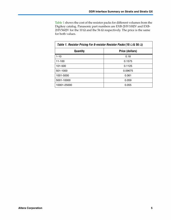
Table 1 shows the cost of the resistor packs for different volumes from the Digikey catalog. Panasonic part numbers are EXB-2HV100JV and EXB-2HV560JV for the 10 Ω and the 56 Ω respectively. The price is the same for both values.
Table 1. Resistor Pricing For 8-resistor Resistor Packs (10 Ω & 56 Ω)
Quantity Price (dollars)
1-10 0.18
11-100 0.1575
101-500 0.1125
501-1000 0.09675
1001-5000 0.061
5001-10000 0.059
10001-25000 0.055
Altera Corporation 5Preliminary

Using External Series and Parallel Termination with Stratix and Stratix GX Devices
Figure 4. Termination of DDR Signals Using Resistor Packs
Board Implementation
The DDR DIMM memory interface was designed in the Stratix GX Development Board. It was designed with the recommended termination scheme. The DDR DIMM interface on the board performs well at 200 MHz. Additionally, the Stratix PCI Board also has the DDR DIMM memory interface running at over 200 MHz. Both boards are currently shipping.
Stratix GX Development Board Schematics
1 The complete schematics of the Stratix GX Development Board are available. Please contact your local Field Applications Engineer (FAE) or Altera Applications for complete schematics.
6 Altera CorporationPreliminary

Board Implementation
Figures 2 and 3 display the summary schematics showing the termination scheme.
Stratix GX Development Board Layout
1 The layout file of the Stratix GX Development Board is available. Please contact your local Field Applications Engineer (FAE) or Altera Applications for the complete layout data.
Figures 5 and 6 show the layout of the Stratix GX device and the DDR DIMM connector on the Stratix GX Development Board.
As per Micron's recommendations, the series resistors need to be placed as close to the DDR DIMM as possible. The parallel (pull up) resistors need to be placed in "fly-by" mode close to the DDR DIMM. Figures 2 , 3 , and 4 provide pictorial representations of the resistor placement including the fly-by resistor locations.
Altera Corporation 7Preliminary

Using External Series and Parallel Termination with Stratix and Stratix GX Devices
Figure 5. Stratix GX Development Board with the locations of the Stratix GX Device and the DDR DIMM
8 Altera CorporationPreliminary

Board Implementation
Figure 6. Zoomed in view of the top (upper photo) and the bottom (lower photo) of the board showing the termination resistor placement
Altera Corporation 9Preliminary

Using External Series and Parallel Termination with Stratix and Stratix GX Devices
Simulation and Measurement Correlation
The Stratix GX Development Board DDR DIMM interface was simulated for signal integrity. This section presents the simulation data and its correlation to the measured signals.
Simulation Procedure
The simulation tool used was ADS Momentum, which is a 2.5D simulator from Agilent Technologies. For maximum accuracy, the simulation was performed on the final routed board ("post layout simulation") as opposed to the pre-routed board ("pre layout simulation"). Data bit 0 and address bit 0 were used as representative cases for this simulation. All other data and address bits should be fairly close in performance to these, since the address, data, data mask and data strobe line lengths were matched on the boards.
The following steps summarize the simulation procedure:
1. The entire Allegro board database (.brd) file was used to produce Gerber output data.
2. The Gerber data for each layer was brought to GBRUNION tool from Artwork Conversion Software. GBRUNION was used to produce .EGS archive file format output.
3. The .EGS file from GBRUNION was brought into Agilent ADS tool.
4. The selected signal and the relevant layers were chosen and other signals and layers that were not relevant were deleted to keep the simulation time manageable. Also, any resistors that were represented by open circuits in the Gerber data were replaced with series RLC models.
5. A post layout frequency domain simulation was performed in ADS Momentum.
6. The frequency domain results from Step 5 were brought into the ADS Schematic in preparation for a time domain simulation.
7. Time domain simulation was performed on ADS Schematic at 200 MHz.
Test Setup
For this test, the DDR DIMM Quartus® II design (including the DDR IP core) was loaded into the Stratix GX device on the Stratix GX Development Board using a JTAG interface. The design was configured
10 Altera CorporationPreliminary

Simulation and Measurement Correlation
to write data to the DDR DIMM and read it back at 200 MHz or 400 Mbps. Nios® soft core processor was used to control the pattern of data written. Figure 7 shows the lab bench setup.
Figure 7. Lab Bench Setup for the Test
The scope used was 6 GHz real-time scope (WaveMaster 8600A) from LeCroy and the probe used was 2.5 GHz active probe HFP2500 also from LeCroy.
Altera Corporation 11Preliminary

Using External Series and Parallel Termination with Stratix and Stratix GX Devices
Data 0 Correlation
The scope shots were taken at the DDR DIMM connector pin and the Stratix GX device at the corresponding pins. These screen captures display the interface running at 200 MHz. The test being run for these captures was writing a "worst-case" data pattern of "1010" on each data line of the bus in a long burst and then reading this pattern back in a long burst.
Figure 8 shows the correlation between the measured and simulated waveforms. The correlation is very good.
The fixed time shifts should not be considered in those correlations because there can be a time offset between for the simulated and measured waveform.
Figure 8. Correlation between Measured and Simulated Waveforms
12 Altera CorporationPreliminary

Conclusion
Address 0 Correlation
Figure 9 shows the correlation between simulated and measured address waveforms at the DDR DIMM pin. The scope captures were taken at the DDR DIMM connector pin and the Stratix GX device at the corresponding pins.
The fixed time shifts should not be considered in those correlations because there can be a time offset between the simulated and measured waveform.
Figure 9. Correlation Between Measured and Simulated "Address" Waveforms at the DDR DIMM Pin
Conclusion To conclude, external resistors can be used to implement termination for Altera's devices. This document shows the DDR DIMM memory interface on the Stratix GX Development Board as a specific example. The resistors are available in very small footprints and cost only $1.40 for the entire 25.6 Gbps throughput DDR DIMM interface. Simulated and measured results show good correlation proving the validity of the approach. Performance of the DDR DIMM interface at 200 MHz (400 Mbps) has been achieved on the Stratix GX Development and Stratix PCI Boards and these boards are currently shipping.
Altera Corporation 13Preliminary

Using External Series and Parallel Termination with Stratix and Stratix GX Devices
We recommend you follow the termination scheme provided in this document for your designs.
14 Altera CorporationPreliminary
101 Innovation DriveSan Jose, CA 95134(408) 544-7000www.altera.comApplications Hotline:(800) 800-EPLDLiterature Services:[email protected]
Copyright © 2003 Altera Corporation. All rights reserved. Altera, The Programmable Solutions Company,the stylized Altera logo, specific device designations, and all other words and logos that are identified astrademarks and/or service marks are, unless noted otherwise, the trademarks and service marks of AlteraCorporation in the U.S. and other countries. All other product or service names are the property of their re-spective holders. Altera products are protected under numerous U.S. and foreign patents and pendingapplications, maskwork rights, and copyrights. Altera warrants performance of its semiconductor productsto current specifications in accordance with Altera's standard warranty, but reserves the right to make chang-es to any products and services at any time without notice. Altera assumes no responsibility or liabilityarising out of the application or use of any information, product, or service describedherein except as expressly agreed to in writing by Altera Corporation. Altera customersare advised to obtain the latest version of device specifications before relying on any pub-lished information and before placing orders for products or services.
Printed on recycled paper