usb3315c - hi-speed usb transceiver with 1.8v-3.3v...
TRANSCRIPT
SMSC USB3315 REV CDATASHE
PRODUCT FEATURES
USB3315
Hi-Speed USB Transceiver with 1.8V-3.3V ULPI Interface - 24MHz Reference Clock
Datasheet
USB-IF “Hi-Speed” compliant to the Universal Serial Bus Specification Rev 2.0Interface compliant with the ULPI Specification revision 1.1 as a Single Data Rate (SDR) PHY1.8V to 3.3V IO Voltage (±10%)flexPWR® Technology— Low current design ideal for battery powered
applications— “Sleep” mode tri-states all ULPI pins and places the
part in a low current stateSupports FS pre-amble for FS hubs with a LS device attached (UTMI+ Level 3)Supports HS SOF and LS keep-alive pulseIncludes full support for the optional On-The-Go (OTG) protocol detailed in the On-The-Go Supplement Revision 2.0 specificationSupports the OTG Host Negotiation Protocol (HNP) and Session Request Protocol (SRP)Allows host to turn VBUS off to conserve battery power in OTG applicationsSupport OTG monitoring of VBUS levels with internal comparators“Wrapper-less” design for optimal timing performance and design ease— Low Latency Hi-Speed Receiver (43 Hi-Speed clocks
Max) allows use of legacy UTMI Links with a ULPI bridge
Internal 5V cable short-circuit protection of ID, DP and DM lines to VBUS or ground24MHz Reference Clock Operation— 0 to 3.6V input drive tolerant— Able to accept “noisy” clock sourcesInternal low jitter PLL for 480MHz Hi-Speed USB operationInternal detection of the value of resistance to ground on the ID pinIntegrated battery to 3.3V LDO regulator— 2.2uF bypass capacitor— 100mV dropout voltageIntegrated ESD protection circuits— Up to ±15kV without any external devices
Carkit UART mode for non-USB serial data transfersIndustrial Operating Temperature -40°C to +85°CPackaging Options— 24 pin QFN lead-free RoHS compliant package
(4 x 4 x 0.90 mm height)
Applications
The USB3315 is targeted for any application where a Hi-Speed USB connection is desired and when boardspace, power, and interface pins must be minimized.
The USB3315 is well suited for:Cell PhonesPDAsMP3 PlayersGPS Personal NavigationScannersExternal Hard DrivesDigital Still and Video CamerasPortable Media PlayersEntertainment DevicesPrintersSet Top BoxesVideo Record/Playback SystemsIP and Video PhonesGaming ConsolesPOS Terminals
Revision 2.1 (06-02-10) ET
Hi-Speed USB Transceiver with 1.8V-3.3V ULPI Interface - 24MHz Reference Clock
Datasheet
Order Number(s):
USB3315C-CP-TR FOR 24 PIN, QFN LEAD-FREE ROHS COMPLIANT PACKAGE (TAPE AND REEL)REEL SIZE IS 4000 PIECES.
This product meets the halogen maximum concentration values per IEC61249-2-21
For RoHS compliance and environmental information, please visit www.smsc.com/rohs
80 ARKAY DRIVE, HAUPPAUGE, NY 11788 (631) 435-6000, FAX (631) 273-3123
Copyright © 2010 SMSC or its subsidiaries. All rights reserved.
Circuit diagrams and other information relating to SMSC products are included as a means of illustrating typical applications. Consequently, complete information sufficient forconstruction purposes is not necessarily given. Although the information has been checked and is believed to be accurate, no responsibility is assumed for inaccuracies. SMSCreserves the right to make changes to specifications and product descriptions at any time without notice. Contact your local SMSC sales office to obtain the latest specificationsbefore placing your product order. The provision of this information does not convey to the purchaser of the described semiconductor devices any licenses under any patentrights or other intellectual property rights of SMSC or others. All sales are expressly conditional on your agreement to the terms and conditions of the most recently datedversion of SMSC's standard Terms of Sale Agreement dated before the date of your order (the "Terms of Sale Agreement"). The product may contain design defects or errorsknown as anomalies which may cause the product's functions to deviate from published specifications. Anomaly sheets are available upon request. SMSC products are notdesigned, intended, authorized or warranted for use in any life support or other application where product failure could cause or contribute to personal injury or severe propertydamage. Any and all such uses without prior written approval of an Officer of SMSC and further testing and/or modification will be fully at the risk of the customer. Copies ofthis document or other SMSC literature, as well as the Terms of Sale Agreement, may be obtained by visiting SMSC’s website at http://www.smsc.com. SMSC is a registeredtrademark of Standard Microsystems Corporation (“SMSC”). Product names and company names are the trademarks of their respective holders.
SMSC DISCLAIMS AND EXCLUDES ANY AND ALL WARRANTIES, INCLUDING WITHOUT LIMITATION ANY AND ALL IMPLIED WARRANTIES OF MERCHANTABILITY,FITNESS FOR A PARTICULAR PURPOSE, TITLE, AND AGAINST INFRINGEMENT AND THE LIKE, AND ANY AND ALL WARRANTIES ARISING FROM ANY COURSEOF DEALING OR USAGE OF TRADE. IN NO EVENT SHALL SMSC BE LIABLE FOR ANY DIRECT, INCIDENTAL, INDIRECT, SPECIAL, PUNITIVE, OR CONSEQUENTIALDAMAGES; OR FOR LOST DATA, PROFITS, SAVINGS OR REVENUES OF ANY KIND; REGARDLESS OF THE FORM OF ACTION, WHETHER BASED ON CONTRACT;TORT; NEGLIGENCE OF SMSC OR OTHERS; STRICT LIABILITY; BREACH OF WARRANTY; OR OTHERWISE; WHETHER OR NOT ANY REMEDY OF BUYER IS HELDTO HAVE FAILED OF ITS ESSENTIAL PURPOSE, AND WHETHER OR NOT SMSC HAS BEEN ADVISED OF THE POSSIBILITY OF SUCH DAMAGES.
Revision 2.1 (06-02-10) 2 SMSC USB3315 REV CDATASHEET
Hi-Speed USB Transceiver with 1.8V-3.3V ULPI Interface - 24MHz Reference Clock
Datasheet
0.1 Reference DocumentsUniversal Serial Bus Specification, Revision 2.0, April 27, 2000
On-The-Go Supplement to the USB 2.0 Specification, Revision 2.0, May 8, 2009
27% Resistor ECN
USB 2.0 Transceiver Macrocell Interface (UTMI) Specification, Version 1.02, May 27, 2000
UTMI+ Specification, Revision 1.0, February 2, 2004
UTMI+ Low Pin Interface (ULPI) Specification, Revision 1.1, October 20, 2004
Technical Requirements and Test Methods of Charger and Interface for Mobile Telecommunication Terminal Equipment (Chinese Charger Specification Approval Draft 11/29/2006)
SMSC USB3315 REV C 3 Revision 2.1 (06-02-10)DATASHEET
Hi-Speed USB Transceiver with 1.8V-3.3V ULPI Interface - 24MHz Reference Clock
Datasheet
Table of Contents0.1 Reference Documents . . . . . . . . . . . . . . . . . . . . . . . . . . . . . . . . . . . . . . . . . . . . . . . . . . . . . . . . . . . 3
Chapter 1 General Description. . . . . . . . . . . . . . . . . . . . . . . . . . . . . . . . . . . . . . . . . . . . . . . . . 8
Chapter 2 USB3315 Pin Locations and Definitions . . . . . . . . . . . . . . . . . . . . . . . . . . . . . . . . 92.1 USB3315 Pin Locations and Descriptions . . . . . . . . . . . . . . . . . . . . . . . . . . . . . . . . . . . . . . . . . . . . 9
2.1.1 Package Diagram with Pin Locations . . . . . . . . . . . . . . . . . . . . . . . . . . . . . . . . . . . . . . . . 92.1.2 Pin Definitions . . . . . . . . . . . . . . . . . . . . . . . . . . . . . . . . . . . . . . . . . . . . . . . . . . . . . . . . . . 9
Chapter 3 Limiting Values . . . . . . . . . . . . . . . . . . . . . . . . . . . . . . . . . . . . . . . . . . . . . . . . . . . 123.1 Absolute Maximum Ratings . . . . . . . . . . . . . . . . . . . . . . . . . . . . . . . . . . . . . . . . . . . . . . . . . . . . . . 123.2 Recommended Operating Conditions. . . . . . . . . . . . . . . . . . . . . . . . . . . . . . . . . . . . . . . . . . . . . . . 13
Chapter 4 Electrical Characteristics . . . . . . . . . . . . . . . . . . . . . . . . . . . . . . . . . . . . . . . . . . . 144.1 Operating Current . . . . . . . . . . . . . . . . . . . . . . . . . . . . . . . . . . . . . . . . . . . . . . . . . . . . . . . . . . . . . . 144.2 CLKOUT Specifications . . . . . . . . . . . . . . . . . . . . . . . . . . . . . . . . . . . . . . . . . . . . . . . . . . . . . . . . . 154.3 ULPI Interface Timing . . . . . . . . . . . . . . . . . . . . . . . . . . . . . . . . . . . . . . . . . . . . . . . . . . . . . . . . . . . 154.4 Digital IO Pins . . . . . . . . . . . . . . . . . . . . . . . . . . . . . . . . . . . . . . . . . . . . . . . . . . . . . . . . . . . . . . . . . 154.5 DC Characteristics: Analog I/O Pins. . . . . . . . . . . . . . . . . . . . . . . . . . . . . . . . . . . . . . . . . . . . . . . . 164.6 Dynamic Characteristics: Analog I/O Pins . . . . . . . . . . . . . . . . . . . . . . . . . . . . . . . . . . . . . . . . . . . 184.7 OTG Electrical Characteristics . . . . . . . . . . . . . . . . . . . . . . . . . . . . . . . . . . . . . . . . . . . . . . . . . . . . 184.8 Regulator Output Voltages and Capacitor Requirement . . . . . . . . . . . . . . . . . . . . . . . . . . . . . . . . 19
Chapter 5 Architecture Overview . . . . . . . . . . . . . . . . . . . . . . . . . . . . . . . . . . . . . . . . . . . . . 205.1 ULPI Digital Operation and Interface . . . . . . . . . . . . . . . . . . . . . . . . . . . . . . . . . . . . . . . . . . . . . . . 205.2 Interface to DP/DM . . . . . . . . . . . . . . . . . . . . . . . . . . . . . . . . . . . . . . . . . . . . . . . . . . . . . . . . . . . . . 20
5.2.1 USB Transceiver . . . . . . . . . . . . . . . . . . . . . . . . . . . . . . . . . . . . . . . . . . . . . . . . . . . . . . . 205.2.2 Termination Resistors . . . . . . . . . . . . . . . . . . . . . . . . . . . . . . . . . . . . . . . . . . . . . . . . . . . 21
5.3 Bias Generator . . . . . . . . . . . . . . . . . . . . . . . . . . . . . . . . . . . . . . . . . . . . . . . . . . . . . . . . . . . . . . . . 235.4 Integrated Low Jitter PLL . . . . . . . . . . . . . . . . . . . . . . . . . . . . . . . . . . . . . . . . . . . . . . . . . . . . . . . . 23
5.4.1 Reference Clock Requirements. . . . . . . . . . . . . . . . . . . . . . . . . . . . . . . . . . . . . . . . . . . . 235.5 Internal Regulators and POR . . . . . . . . . . . . . . . . . . . . . . . . . . . . . . . . . . . . . . . . . . . . . . . . . . . . . 24
5.5.1 Integrated Low Dropout Regulator . . . . . . . . . . . . . . . . . . . . . . . . . . . . . . . . . . . . . . . . . 245.5.2 Power On Reset (POR) . . . . . . . . . . . . . . . . . . . . . . . . . . . . . . . . . . . . . . . . . . . . . . . . . . 265.5.3 Recommended Power Supply Sequence . . . . . . . . . . . . . . . . . . . . . . . . . . . . . . . . . . . . 265.5.4 Start-Up . . . . . . . . . . . . . . . . . . . . . . . . . . . . . . . . . . . . . . . . . . . . . . . . . . . . . . . . . . . . . . 27
5.6 USB On-The-Go (OTG) . . . . . . . . . . . . . . . . . . . . . . . . . . . . . . . . . . . . . . . . . . . . . . . . . . . . . . . . . 285.6.1 ID Resistor Detection. . . . . . . . . . . . . . . . . . . . . . . . . . . . . . . . . . . . . . . . . . . . . . . . . . . . 295.6.2 VBUS Monitor and Pulsing . . . . . . . . . . . . . . . . . . . . . . . . . . . . . . . . . . . . . . . . . . . . . . . 315.6.3 Driving External Vbus . . . . . . . . . . . . . . . . . . . . . . . . . . . . . . . . . . . . . . . . . . . . . . . . . . . 33
5.7 USB UART Support . . . . . . . . . . . . . . . . . . . . . . . . . . . . . . . . . . . . . . . . . . . . . . . . . . . . . . . . . . . . 345.8 USB Charger Detection Support. . . . . . . . . . . . . . . . . . . . . . . . . . . . . . . . . . . . . . . . . . . . . . . . . . . 34
Chapter 6 ULPI Operation Overview . . . . . . . . . . . . . . . . . . . . . . . . . . . . . . . . . . . . . . . . . . 356.1 Overview. . . . . . . . . . . . . . . . . . . . . . . . . . . . . . . . . . . . . . . . . . . . . . . . . . . . . . . . . . . . . . . . . . . . . 35
6.1.1 ULPI Interface Signals . . . . . . . . . . . . . . . . . . . . . . . . . . . . . . . . . . . . . . . . . . . . . . . . . . . 366.1.2 ULPI Interface Timing in Synchronous Mode . . . . . . . . . . . . . . . . . . . . . . . . . . . . . . . . . 37
6.2 ULPI Register Access. . . . . . . . . . . . . . . . . . . . . . . . . . . . . . . . . . . . . . . . . . . . . . . . . . . . . . . . . . . 376.2.1 ULPI Register Write . . . . . . . . . . . . . . . . . . . . . . . . . . . . . . . . . . . . . . . . . . . . . . . . . . . . . 386.2.2 ULPI Register Read. . . . . . . . . . . . . . . . . . . . . . . . . . . . . . . . . . . . . . . . . . . . . . . . . . . . . 406.2.3 ULPI RXCMD . . . . . . . . . . . . . . . . . . . . . . . . . . . . . . . . . . . . . . . . . . . . . . . . . . . . . . . . . 416.2.4 USB3315 Transmitter . . . . . . . . . . . . . . . . . . . . . . . . . . . . . . . . . . . . . . . . . . . . . . . . . . . 42
Revision 2.1 (06-02-10) 4 SMSC USB3315 REV CDATASHEET
Hi-Speed USB Transceiver with 1.8V-3.3V ULPI Interface - 24MHz Reference Clock
Datasheet
6.2.5 USB Receiver . . . . . . . . . . . . . . . . . . . . . . . . . . . . . . . . . . . . . . . . . . . . . . . . . . . . . . . . . 446.2.6 Low Power Mode. . . . . . . . . . . . . . . . . . . . . . . . . . . . . . . . . . . . . . . . . . . . . . . . . . . . . . . 45
6.3 Full Speed/Low Speed Serial Modes . . . . . . . . . . . . . . . . . . . . . . . . . . . . . . . . . . . . . . . . . . . . . . . 486.3.1 3pin FS/LS Serial Mode. . . . . . . . . . . . . . . . . . . . . . . . . . . . . . . . . . . . . . . . . . . . . . . . . . 496.3.2 6pin FS/LS Serial Mode. . . . . . . . . . . . . . . . . . . . . . . . . . . . . . . . . . . . . . . . . . . . . . . . . . 49
6.4 Carkit Mode . . . . . . . . . . . . . . . . . . . . . . . . . . . . . . . . . . . . . . . . . . . . . . . . . . . . . . . . . . . . . . . . . . 506.4.1 USB UART Mode . . . . . . . . . . . . . . . . . . . . . . . . . . . . . . . . . . . . . . . . . . . . . . . . . . . . . . 50
6.5 RID Converter Operation . . . . . . . . . . . . . . . . . . . . . . . . . . . . . . . . . . . . . . . . . . . . . . . . . . . . . . . . 506.6 Headset Audio Mode . . . . . . . . . . . . . . . . . . . . . . . . . . . . . . . . . . . . . . . . . . . . . . . . . . . . . . . . . . . 51
Chapter 7 ULPI Register Map . . . . . . . . . . . . . . . . . . . . . . . . . . . . . . . . . . . . . . . . . . . . . . . . 537.1 ULPI Register Array . . . . . . . . . . . . . . . . . . . . . . . . . . . . . . . . . . . . . . . . . . . . . . . . . . . . . . . . . . . . 53
7.1.1 ULPI Register Set . . . . . . . . . . . . . . . . . . . . . . . . . . . . . . . . . . . . . . . . . . . . . . . . . . . . . . 547.1.2 Carkit Control Registers . . . . . . . . . . . . . . . . . . . . . . . . . . . . . . . . . . . . . . . . . . . . . . . . . 597.1.3 Extended Register Access . . . . . . . . . . . . . . . . . . . . . . . . . . . . . . . . . . . . . . . . . . . . . . . 617.1.4 Vendor Register Access . . . . . . . . . . . . . . . . . . . . . . . . . . . . . . . . . . . . . . . . . . . . . . . . . 61
Chapter 8 Application Notes . . . . . . . . . . . . . . . . . . . . . . . . . . . . . . . . . . . . . . . . . . . . . . . . . . 648.1 Application Diagram . . . . . . . . . . . . . . . . . . . . . . . . . . . . . . . . . . . . . . . . . . . . . . . . . . . . . . . . . . . . 648.2 USB Charger Detection . . . . . . . . . . . . . . . . . . . . . . . . . . . . . . . . . . . . . . . . . . . . . . . . . . . . . . . . . 66
8.2.1 Detecting the ID Resistor in a Charger . . . . . . . . . . . . . . . . . . . . . . . . . . . . . . . . . . . . . . 668.2.2 Detecting DP Shorted to DM . . . . . . . . . . . . . . . . . . . . . . . . . . . . . . . . . . . . . . . . . . . . . . 67
8.3 Reference Designs . . . . . . . . . . . . . . . . . . . . . . . . . . . . . . . . . . . . . . . . . . . . . . . . . . . . . . . . . . . . . 678.4 ESD Performance. . . . . . . . . . . . . . . . . . . . . . . . . . . . . . . . . . . . . . . . . . . . . . . . . . . . . . . . . . . . . . 67
8.4.1 Human Body Model (HBM) Performance . . . . . . . . . . . . . . . . . . . . . . . . . . . . . . . . . . . . 678.4.2 EN/IEC 61000-4-2 Performance . . . . . . . . . . . . . . . . . . . . . . . . . . . . . . . . . . . . . . . . . . . 688.4.3 Air Discharge . . . . . . . . . . . . . . . . . . . . . . . . . . . . . . . . . . . . . . . . . . . . . . . . . . . . . . . . . . 688.4.4 Contact Discharge . . . . . . . . . . . . . . . . . . . . . . . . . . . . . . . . . . . . . . . . . . . . . . . . . . . . . . 68
Chapter 9 Package Outline, Tape & Reel Drawings, Package Markings . . . . . . . . . . . . . 69
Chapter 10 Datasheet Revision History . . . . . . . . . . . . . . . . . . . . . . . . . . . . . . . . . . . . . . . . . . 73
SMSC USB3315 REV C 5 Revision 2.1 (06-02-10)DATASHEET
Hi-Speed USB Transceiver with 1.8V-3.3V ULPI Interface - 24MHz Reference Clock
Datasheet
Revision 2.1 (06-02-10) 6 SMSC USB3315 REV CDATASHEET
List of FiguresFigure 1.1 USB3315 Block Diagram . . . . . . . . . . . . . . . . . . . . . . . . . . . . . . . . . . . . . . . . . . . . . . . . . . . . . 8Figure 2.1 USB3315 QFN Pinout - Top View . . . . . . . . . . . . . . . . . . . . . . . . . . . . . . . . . . . . . . . . . . . . . . 9Figure 4.1 External Reference Clock . . . . . . . . . . . . . . . . . . . . . . . . . . . . . . . . . . . . . . . . . . . . . . . . . . . 16Figure 5.1 USB3315 System Diagram . . . . . . . . . . . . . . . . . . . . . . . . . . . . . . . . . . . . . . . . . . . . . . . . . . 20Figure 5.2 Example of circuit used to shift a reference clock common-mode voltage level. . . . . . . . . . . 23Figure 5.3 USB3315 Allowable REFCLK Jitter vs. Frequency . . . . . . . . . . . . . . . . . . . . . . . . . . . . . . . . 24Figure 5.4 Powering the USB3315 from a Battery . . . . . . . . . . . . . . . . . . . . . . . . . . . . . . . . . . . . . . . . . 25Figure 5.5 Powering the USB3315 from a 3.3V Supply . . . . . . . . . . . . . . . . . . . . . . . . . . . . . . . . . . . . . 25Figure 5.6 Powering the USB3315 from the USB Cable Vbus . . . . . . . . . . . . . . . . . . . . . . . . . . . . . . . . 26Figure 5.7 ULPI Start-up Timing . . . . . . . . . . . . . . . . . . . . . . . . . . . . . . . . . . . . . . . . . . . . . . . . . . . . . . . 28Figure 5.8 USB3315 ID Resistor Detection Circuitry. . . . . . . . . . . . . . . . . . . . . . . . . . . . . . . . . . . . . . . . 29Figure 5.9 USB3315 OTG Vbus Block . . . . . . . . . . . . . . . . . . . . . . . . . . . . . . . . . . . . . . . . . . . . . . . . . . 31Figure 5.10 USB3315 Drives External Vbus Supply or Switch . . . . . . . . . . . . . . . . . . . . . . . . . . . . . . . . . 33Figure 6.1 ULPI Digital Block Diagram . . . . . . . . . . . . . . . . . . . . . . . . . . . . . . . . . . . . . . . . . . . . . . . . . . 35Figure 6.2 ULPI Single Data Rate Timing Diagram in Synchronous Mode. . . . . . . . . . . . . . . . . . . . . . . 37Figure 6.3 ULPI Register Write in Synchronous Mode . . . . . . . . . . . . . . . . . . . . . . . . . . . . . . . . . . . . . . 38Figure 6.4 ULPI Extended Register Write in Synchronous Mode . . . . . . . . . . . . . . . . . . . . . . . . . . . . . . 39Figure 6.5 ULPI Register Read in Synchronous Mode . . . . . . . . . . . . . . . . . . . . . . . . . . . . . . . . . . . . . . 40Figure 6.6 ULPI Extended Register Read in Synchronous Mode . . . . . . . . . . . . . . . . . . . . . . . . . . . . . . 41Figure 6.7 ULPI Transmit in Synchronous Mode . . . . . . . . . . . . . . . . . . . . . . . . . . . . . . . . . . . . . . . . . . 44Figure 6.8 ULPI Receive in Synchronous Mode . . . . . . . . . . . . . . . . . . . . . . . . . . . . . . . . . . . . . . . . . . . 45Figure 6.9 Entering Low Power Mode from Synchronous Mode. . . . . . . . . . . . . . . . . . . . . . . . . . . . . . . 46Figure 6.10 Exiting Low Power Mode . . . . . . . . . . . . . . . . . . . . . . . . . . . . . . . . . . . . . . . . . . . . . . . . . . . . 47Figure 8.1 USB3315 QFN Application Diagram (Device) . . . . . . . . . . . . . . . . . . . . . . . . . . . . . . . . . . . . 65Figure 8.2 USB3315 QFN Application Diagram (Host or OTG) . . . . . . . . . . . . . . . . . . . . . . . . . . . . . . . 66Figure 9.1 24-pin QFN, 4x4mm Body, 0.5mm Pitch . . . . . . . . . . . . . . . . . . . . . . . . . . . . . . . . . . . . . . . . 69Figure 9.2 QFN, 4x4 Tape & Reel. . . . . . . . . . . . . . . . . . . . . . . . . . . . . . . . . . . . . . . . . . . . . . . . . . . . . . 70Figure 9.3 Reel Dimensions . . . . . . . . . . . . . . . . . . . . . . . . . . . . . . . . . . . . . . . . . . . . . . . . . . . . . . . . . . 71Figure 9.4 QFN, 4x4 Package Marking . . . . . . . . . . . . . . . . . . . . . . . . . . . . . . . . . . . . . . . . . . . . . . . . . . 72
Hi-Speed USB Transceiver with 1.8V-3.3V ULPI Interface - 24MHz Reference Clock
Datasheet
SMSC USB3315 REV C 7 Revision 2.1 (06-02-10)DATASHEET
List of TablesTable 2.1 USB3315 Pin Description . . . . . . . . . . . . . . . . . . . . . . . . . . . . . . . . . . . . . . . . . . . . . . . . . . . . . . . . . . . . . . 9Table 3.1 Absolute Maximum Ratings . . . . . . . . . . . . . . . . . . . . . . . . . . . . . . . . . . . . . . . . . . . . . . . . . . . . . . . . . . . 12Table 3.2 Recommended Operating Conditions. . . . . . . . . . . . . . . . . . . . . . . . . . . . . . . . . . . . . . . . . . . . . . . . . . . . 13Table 4.1 Electrical Characteristics: Operating Current . . . . . . . . . . . . . . . . . . . . . . . . . . . . . . . . . . . . . . . . . . . . . . 14Table 4.2 Electrical Characteristics: CLKOUT Specifications. . . . . . . . . . . . . . . . . . . . . . . . . . . . . . . . . . . . . . . . . . 15Table 4.3 ULPI Interface Timing . . . . . . . . . . . . . . . . . . . . . . . . . . . . . . . . . . . . . . . . . . . . . . . . . . . . . . . . . . . . . . . . 15Table 4.4 Digital IO Characteristics: RESETB, CLKOUT, STP, DIR, NXT, DATA[7:0] and XI Pins. . . . . . . . . . . . . 15Table 4.5 DC Characteristics: Analog I/O Pins (DP/DM) . . . . . . . . . . . . . . . . . . . . . . . . . . . . . . . . . . . . . . . . . . . . . 16Table 4.6 Dynamic Characteristics: Analog I/O Pins (DP/DM) . . . . . . . . . . . . . . . . . . . . . . . . . . . . . . . . . . . . . . . . . 18Table 4.7 OTG Electrical Characteristics . . . . . . . . . . . . . . . . . . . . . . . . . . . . . . . . . . . . . . . . . . . . . . . . . . . . . . . . . 18Table 4.8 Regulator Output Voltages and Capacitor Requirement . . . . . . . . . . . . . . . . . . . . . . . . . . . . . . . . . . . . . 19Table 4.9 ESD and LATCH-UP Performance. . . . . . . . . . . . . . . . . . . . . . . . . . . . . . . . . . . . . . . . . . . . . . . . . . . . . . 19Table 5.1 DP/DM Termination vs. Signaling Mode. . . . . . . . . . . . . . . . . . . . . . . . . . . . . . . . . . . . . . . . . . . . . . . . . . 21Table 5.2 Operating Mode vs. Power Supply Configuration. . . . . . . . . . . . . . . . . . . . . . . . . . . . . . . . . . . . . . . . . . . 27Table 5.3 Valid Values of ID Resistance to Ground . . . . . . . . . . . . . . . . . . . . . . . . . . . . . . . . . . . . . . . . . . . . . . . . . 30Table 5.4 IdGnd and IdFloat vs. ID Resistance to Ground . . . . . . . . . . . . . . . . . . . . . . . . . . . . . . . . . . . . . . . . . . . . 30Table 5.5 External Vbus Indicator Logic . . . . . . . . . . . . . . . . . . . . . . . . . . . . . . . . . . . . . . . . . . . . . . . . . . . . . . . . . . 32Table 5.6 USB Weak Pull-up Enable . . . . . . . . . . . . . . . . . . . . . . . . . . . . . . . . . . . . . . . . . . . . . . . . . . . . . . . . . . . . 34Table 6.1 ULPI Interface Signals . . . . . . . . . . . . . . . . . . . . . . . . . . . . . . . . . . . . . . . . . . . . . . . . . . . . . . . . . . . . . . . 36Table 6.2 ULPI TXD CMD Byte Encoding . . . . . . . . . . . . . . . . . . . . . . . . . . . . . . . . . . . . . . . . . . . . . . . . . . . . . . . . 38Table 6.3 ULPI RX CMD Encoding. . . . . . . . . . . . . . . . . . . . . . . . . . . . . . . . . . . . . . . . . . . . . . . . . . . . . . . . . . . . . . 42Table 6.4 Interface Signal Mapping During Low Power Mode . . . . . . . . . . . . . . . . . . . . . . . . . . . . . . . . . . . . . . . . . 46Table 6.5 Pin Definitions in 3 pin Serial Mode . . . . . . . . . . . . . . . . . . . . . . . . . . . . . . . . . . . . . . . . . . . . . . . . . . . . . 49Table 6.6 Pin Definitions in 6 pin Serial Mode . . . . . . . . . . . . . . . . . . . . . . . . . . . . . . . . . . . . . . . . . . . . . . . . . . . . . 49Table 6.7 Pin Definitions in Carkit Mode. . . . . . . . . . . . . . . . . . . . . . . . . . . . . . . . . . . . . . . . . . . . . . . . . . . . . . . . . . 50Table 6.8 Pin Definitions in Headset Audio Mode . . . . . . . . . . . . . . . . . . . . . . . . . . . . . . . . . . . . . . . . . . . . . . . . . . 51Table 7.1 ULPI Register Map . . . . . . . . . . . . . . . . . . . . . . . . . . . . . . . . . . . . . . . . . . . . . . . . . . . . . . . . . . . . . . . . . . 53Table 8.1 Component Values in Application Diagrams . . . . . . . . . . . . . . . . . . . . . . . . . . . . . . . . . . . . . . . . . . . . . . 64Table 8.2 Capacitance Values at VBUS of USB Connector . . . . . . . . . . . . . . . . . . . . . . . . . . . . . . . . . . . . . . . . . . . 64Table 10.1 Customer Revision History . . . . . . . . . . . . . . . . . . . . . . . . . . . . . . . . . . . . . . . . . . . . . . . . . . . . . . . . . . . . 73
Hi-Speed USB Transceiver with 1.8V-3.3V ULPI Interface - 24MHz Reference Clock
Datasheet
Revision 2.1 (06-02-10) 8 SMSC USB3315 REV CDATASHEET
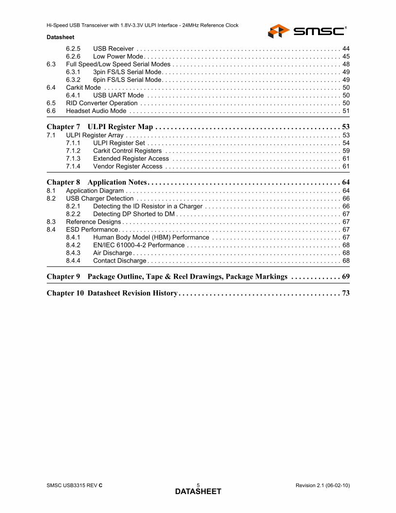
Chapter 1 General Description
The USB3315 is a highly integrated Hi-Speed USB 2.0 Transceiver (PHY) that supports systemsarchitectures based on a 24MHz reference clock. It is designed to be used in both commercial andindustrial temperature applications.
The USB3315 meets all of the electrical requirements to be used as a Hi-Speed USB Host, Device,or an On-the-Go (OTG) device. In addition to the supporting USB signaling the USB3315 also providesUSB UART mode
USB3315 uses the industry standard UTMI+ Low Pin Interface (ULPI) to connect the USB PHY to theLink. The industry standard ULPI interface uses a method of in-band signaling and status byte transfersbetween the Link and PHY, to facilitate a USB session. By using in-band signaling and status bytetransfers the ULPI interface requires only 12 pins.
The USB3315 uses SMSC’s “wrapper-less” technology to implement the ULPI interface. This “wrapper-less” technology allows the PHY to achieve a low latency transmit and receive time. SMSC’s lowlatency transceiver allows an existing UTMI Link to be reused by adding a UTMI to ULPI bridge. Byadding a bridge to the ASIC the existing and proven UTMI Link IP can be reused.
Figure 1.1 USB3315 Block Diagram
The USB3315 is designed to run with a 24MHz reference clock. By using a reference clock from theLink the USB3315 is able to remove the cost of a crystal reference from the design.
The USB3315 includes a integrated 3.3V LDO regulator to generate its own supply from power appliedat the VBAT pin. The voltage on the VBAT pin can range from 3.1 to 5.5V. The regulator dropoutvoltage is less than 100mV which allows the PHY to continue USB signaling when the voltage onVBAT drops to 3.1V. The USB transceiver will continue to operate at lower voltages, although someparameters may be outside the limits of the USB specifications. If the user would like to provide a 3.3Vsupply to the USB3315, the VBAT and VDD33 pins should be connected together as described inSection 5.5.1.
The USB3315 also includes integrated pull-up resistors that can be used for detecting the attachmentof a USB Charger. By sensing the attachment to a USB Charger, a product using the USB3315 cancharge its battery at more than the 500mA allowed when charging from a USB Host as described inSection 8.2.
OTG
Carkit
Hi-Speed USB
Transceiver
ULPI Interface
ULPI Registers and State Machine
BIASLow JitterIntegrated
PLL
Integrated Power
Management
VBUS
ID
DP
DM
RBIAS
RESETB
VDD18VDD33
REFCLK
ES
D P
rote
ctio
n
VBAT
VDDIO
DIRNXTSTP
CLKOUT
DATA[7:0]
CPEN
Hi-Speed USB Transceiver with 1.8V-3.3V ULPI Interface - 24MHz Reference Clock
Datasheet
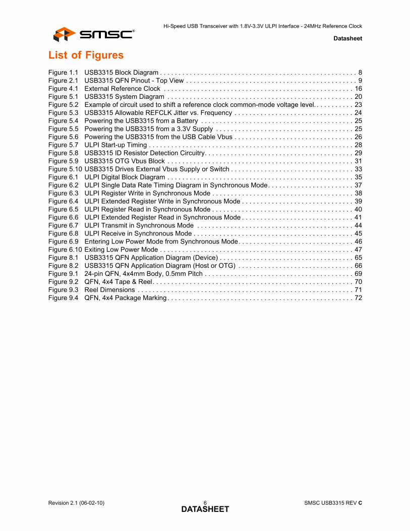
Chapter 2 USB3315 Pin Locations and Definitions
2.1 USB3315 Pin Locations and Descriptions
2.1.1 Package Diagram with Pin Locations
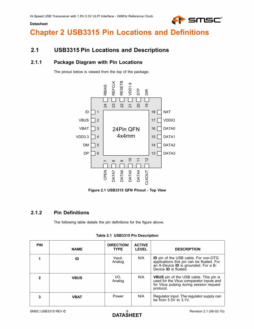
The pinout below is viewed from the top of the package.
Figure 2.1 USB3315 QFN Pinout - Top View
2.1.2 Pin Definitions
The following table details the pin definitions for the figure above.
Table 2.1 USB3315 Pin Description
PINNAME
DIRECTION/TYPE
ACTIVE LEVEL DESCRIPTION
1 ID Input,Analog
N/A ID pin of the USB cable. For non-OTG applications this pin can be floated. For an A-Device ID is grounded. For a B-Device ID is floated.
2 VBUS I/O,Analog
N/A VBUS pin of the USB cable. This pin is used for the Vbus comparator inputs and for Vbus pulsing during session request protocol.
3 VBAT Power N/A Regulator input. The regulator supply can be from 5.5V to 3.1V.
CPE
N
VBUS
ID
VDD3.3
DM
DP
NXT
DIR
STP
CLK
OU
T
DATA0
DATA2
DATA3
DATA1
VBATVD
D1.
8
DA
TA4
DA
TA6
DA
TA7
DA
TA5
1
2
3
4
5
6
7 8 9 10 11 12
18
17
16
15
14
13
24 23 22 21 20 19
24Pin QFN4x4mm
RES
ETB
VDDIO
RBI
AS
REF
CLK
SMSC USB3315 REV C 9 Revision 2.1 (06-02-10)DATASHEET
Hi-Speed USB Transceiver with 1.8V-3.3V ULPI Interface - 24MHz Reference Clock
Datasheet
4 VDD3.3 Power N/A 3.3V Regulator Output. A 2.2uF (<1 ohm ESR) bypass capacitor to ground is required for regulator stability. The bypass capacitor should be placed as close as possible to the USB3315.
5 DM I/O,Analog
N/A D- pin of the USB cable.
6 DP I/O,Analog
N/A D+ pin of the USB cable.
7 CPEN Output,CMOS
High External 5 volt supply enable. This pin is used to enable the external Vbus power supply. The CPEN pin is low on POR. This pad uses VDD3.3 logic level.
8 DATA[7] I/O,CMOS
N/A ULPI bi-directional data bus. DATA[7] is the MSB.
9 DATA[6] I/O,CMOS
N/A ULPI bi-directional data bus.
10 DATA[5 I/O,CMOS
N/A ULPI bi-directional data bus.
11 DATA[4] I/O,CMOS
N/A ULPI bi-directional data bus.
12 CLKOUT Output,CMOS
N/A 60MHz reference clock output. All ULPI signals are driven synchronous to the rising edge of this clock.
Following POR or hardware reset, the voltage at CLKOUT must not exceed VIH_ED as provided in Table 4.4.
13 DATA[3] I/O,CMOS
N/A ULPI bi-directional data bus.
14 DATA[2] I/O,CMOS
N/A ULPI bi-directional data bus.
15 DATA[1] I/O,CMOS
N/A ULPI bi-directional data bus.
16 DATA[0] I/O,CMOS
N/A ULPI bi-directional data bus. DATA[0] is the LSB.
17 VDDIO Power N/A 1.8V to 3.3V ULPI interface supply voltage. This voltage sets the value of VOH for the ULPI interface.
18 NXT Output,CMOS
High The PHY asserts NXT to throttle the data. When the Link is sending data to the PHY, NXT indicates when the current byte has been accepted by the PHY. The Link places the next byte on the data bus in the following clock cycle.
Table 2.1 USB3315 Pin Description (continued)
PINNAME
DIRECTION/TYPE
ACTIVE LEVEL DESCRIPTION
Revision 2.1 (06-02-10) 10 SMSC USB3315 REV CDATASHEET
Hi-Speed USB Transceiver with 1.8V-3.3V ULPI Interface - 24MHz Reference Clock
Datasheet
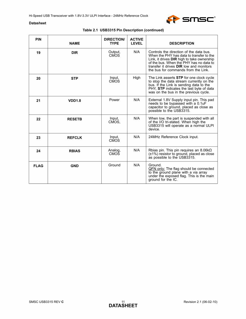
19 DIR Output,CMOS
N/A Controls the direction of the data bus. When the PHY has data to transfer to the Link, it drives DIR high to take ownership of the bus. When the PHY has no data to transfer it drives DIR low and monitors the bus for commands from the Link.
20 STP Input,CMOS
High The Link asserts STP for one clock cycle to stop the data stream currently on the bus. If the Link is sending data to the PHY, STP indicates the last byte of data was on the bus in the previous cycle.
21 VDD1.8 Power N/A External 1.8V Supply input pin. This pad needs to be bypassed with a 0.1uF capacitor to ground, placed as close as possible to the USB3315.
22 RESETB Input,CMOS,
N/A When low, the part is suspended with all of the I/O tri-stated. When high the USB3315 will operate as a normal ULPI device.
23 REFCLK Input,CMOS
N/A 24MHz Reference Clock input.
24 RBIAS Analog,CMOS
N/A Rbias pin. This pin requires an 8.06kΩ (±1%) resistor to ground, placed as close as possible to the USB3315.
FLAG GND Ground N/A Ground.QFN only: The flag should be connected to the ground plane with a via array under the exposed flag. This is the main ground for the IC.
Table 2.1 USB3315 Pin Description (continued)
PINNAME
DIRECTION/TYPE
ACTIVE LEVEL DESCRIPTION
SMSC USB3315 REV C 11 Revision 2.1 (06-02-10)DATASHEET
Hi-Speed USB Transceiver with 1.8V-3.3V ULPI Interface - 24MHz Reference Clock
Datasheet
Chapter 3 Limiting Values
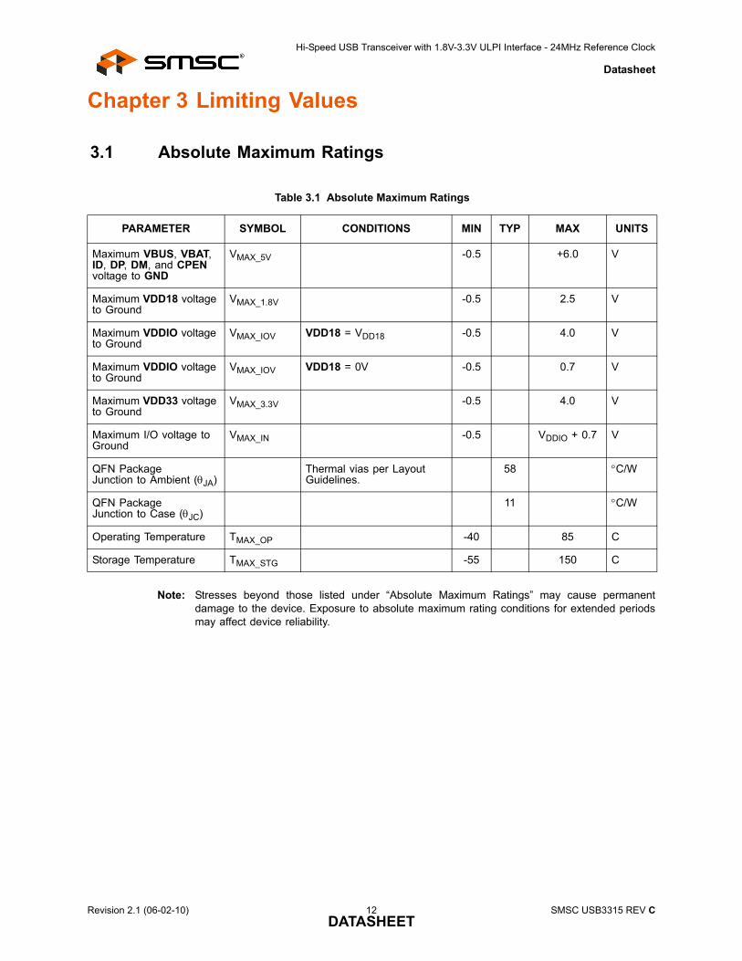
3.1 Absolute Maximum Ratings
Note: Stresses beyond those listed under “Absolute Maximum Ratings” may cause permanentdamage to the device. Exposure to absolute maximum rating conditions for extended periodsmay affect device reliability.
Table 3.1 Absolute Maximum Ratings
PARAMETER SYMBOL CONDITIONS MIN TYP MAX UNITS
Maximum VBUS, VBAT, ID, DP, DM, and CPEN voltage to GND
VMAX_5V -0.5 +6.0 V
Maximum VDD18 voltage to Ground
VMAX_1.8V -0.5 2.5 V
Maximum VDDIO voltage to Ground
VMAX_IOV VDD18 = VDD18 -0.5 4.0 V
Maximum VDDIO voltage to Ground
VMAX_IOV VDD18 = 0V -0.5 0.7 V
Maximum VDD33 voltage to Ground
VMAX_3.3V -0.5 4.0 V
Maximum I/O voltage to Ground
VMAX_IN -0.5 VDDIO + 0.7 V
QFN PackageJunction to Ambient (θJA)
Thermal vias per Layout Guidelines.
58 °C/W
QFN PackageJunction to Case (θJC)
11 °C/W
Operating Temperature TMAX_OP -40 85 C
Storage Temperature TMAX_STG -55 150 C
Revision 2.1 (06-02-10) 12 SMSC USB3315 REV CDATASHEET
Hi-Speed USB Transceiver with 1.8V-3.3V ULPI Interface - 24MHz Reference Clock
Datasheet
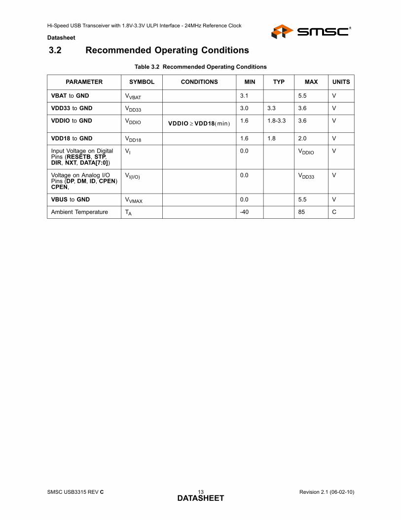
3.2 Recommended Operating ConditionsTable 3.2 Recommended Operating Conditions
PARAMETER SYMBOL CONDITIONS MIN TYP MAX UNITS
VBAT to GND VVBAT 3.1 5.5 V
VDD33 to GND VDD33 3.0 3.3 3.6 V
VDDIO to GND VDDIO 1.6 1.8-3.3 3.6 V
VDD18 to GND VDD18 1.6 1.8 2.0 V
Input Voltage on Digital Pins (RESETB, STP, DIR, NXT, DATA[7:0])
VI 0.0 VDDIO V
Voltage on Analog I/O Pins (DP, DM, ID, CPEN)CPEN,
VI(I/O) 0.0 VDD33 V
VBUS to GND VVMAX 0.0 5.5 V
Ambient Temperature TA -40 85 C
VDDIO VDD18 min( )≥
SMSC USB3315 REV C 13 Revision 2.1 (06-02-10)DATASHEET
Hi-Speed USB Transceiver with 1.8V-3.3V ULPI Interface - 24MHz Reference Clock
Datasheet
Chapter 4 Electrical Characteristics
The following conditions are assumed unless otherwise specified:
VVBAT = 3.1 to 5.5V; VDD18 = 1.6 to 2.0V; VDDIO = 1.6 to 2.0V; VSS = 0V; TA = -40C to +85C
The current for 3.3V circuits is sourced at the VBAT pin, except when using an external 3.3V supplyas shown in Figure 5.5.
4.1 Operating Current
Note 4.1 ClockSuspendM bit = 0.
Note 4.2 SessEnd, VbusVld, and IdFloat comparators disabled. STP Interface protection disabled.
Table 4.1 Electrical Characteristics: Operating Current
PARAMETER SYMBOL CONDITIONS MIN TYP MAX UNITS
Synchronous Mode Current(Default Configuration)
I33AVG(SYNC) Start-up sequence defined in Section 5.5.4 has completed.
5.0 5.5 8.0 mA
I18AVG(SYNC) 17.5 22.0 27.0 mA
IIOAVG(SYNC) 2.5 3.0 4.0 mA
Synchronous Mode Current(HS USB operation)
I33AVG(HS) Active USB Transfer 7.0 10.0 14.0 mA
I18AVG(HS) 23.0 28.0 34.0 mA
IIOAVG(HS) 2.5 3.0 4.0 mA
Synchronous Mode Current(FS/LS USB operation)
I33AVG(FS) Active USB Transfer 5.0 8.5 13.0 mA
I18AVG(FS) 19.0 22.0 27.0 mA
IIOAVG(FS) 2.5 3.0 4.0 mA
Serial Mode Current(FS/LS USB)
Note 4.1
I33AVG(FS_S) 5.0 5.5 7.0 mA
I18AVG(FS_S) 1.5 2.2 3.5 mA
IIOAVG(FS_S) 0.1 mA
USB UART Current
Note 4.1
I33AVG(UART) 5.0 5.5 7.0 mA
I18AVG(UART) 1.4 2.1 3.5 mA
IIOAVG(UART) 0.1 mA
Low Power Mode
Note 4.2
IDD33(LPM) VVBAT = 4.2VVDD18 = 1.8VVDDIO = 1.8V
14.0 20.0 25.0 uA
IDD18(LPM) 0.3 10.0 uA
IDDIO(LPM) 1.5 uA
Standby Mode IDD33(RSTB) RESETB = 0VVBAT = 4.2VVDD18 = 1.8VVDDIO = 1.8V
14.0 20.0 25.0 uA
IDD18(RSTB) 0.3 10.0 uA
IDDIO(RSTB) 1.5 uA
Revision 2.1 (06-02-10) 14 SMSC USB3315 REV CDATASHEET
Hi-Speed USB Transceiver with 1.8V-3.3V ULPI Interface - 24MHz Reference Clock
Datasheet
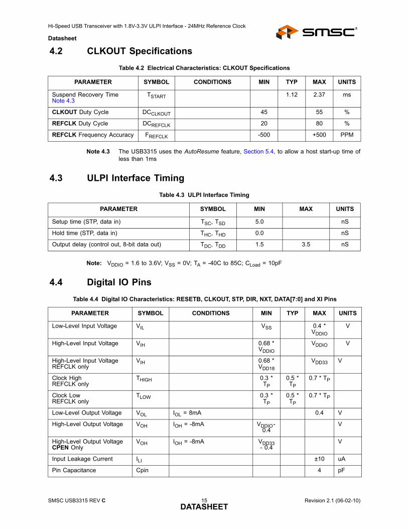
4.2 CLKOUT Specifications
Note 4.3 The USB3315 uses the AutoResume feature, Section 5.4, to allow a host start-up time ofless than 1ms
4.3 ULPI Interface Timing
Note: VDDIO = 1.6 to 3.6V; VSS = 0V; TA = -40C to 85C; CLoad = 10pF
4.4 Digital IO Pins
Table 4.2 Electrical Characteristics: CLKOUT Specifications
PARAMETER SYMBOL CONDITIONS MIN TYP MAX UNITS
Suspend Recovery TimeNote 4.3
TSTART 1.12 2.37 ms
CLKOUT Duty Cycle DCCLKOUT 45 55 %
REFCLK Duty Cycle DCREFCLK 20 80 %
REFCLK Frequency Accuracy FREFCLK -500 +500 PPM
Table 4.3 ULPI Interface Timing
PARAMETER SYMBOL MIN MAX UNITS
Setup time (STP, data in) TSC, TSD 5.0 nS
Hold time (STP, data in) THC, THD 0.0 nS
Output delay (control out, 8-bit data out) TDC, TDD 1.5 3.5 nS
Table 4.4 Digital IO Characteristics: RESETB, CLKOUT, STP, DIR, NXT, DATA[7:0] and XI Pins
PARAMETER SYMBOL CONDITIONS MIN TYP MAX UNITS
Low-Level Input Voltage VIL VSS 0.4 * VDDIO
V
High-Level Input Voltage VIH 0.68 * VDDIO
VDDIO V
High-Level Input VoltageREFCLK only
VIH 0.68 * VDD18
VDD33 V
Clock HighREFCLK only
THIGH 0.3 * TP
0.5 * TP
0.7 * TP
Clock LowREFCLK only
TLOW 0.3 * TP
0.5 * TP
0.7 * TP
Low-Level Output Voltage VOL IOL = 8mA 0.4 V
High-Level Output Voltage VOH IOH = -8mA VDDIO - 0.4
V
High-Level Output VoltageCPEN Only
VOH IOH = -8mA VDD33 - 0.4
V
Input Leakage Current ILI ±10 uA
Pin Capacitance Cpin 4 pF
SMSC USB3315 REV C 15 Revision 2.1 (06-02-10)DATASHEET
Hi-Speed USB Transceiver with 1.8V-3.3V ULPI Interface - 24MHz Reference Clock
Datasheet
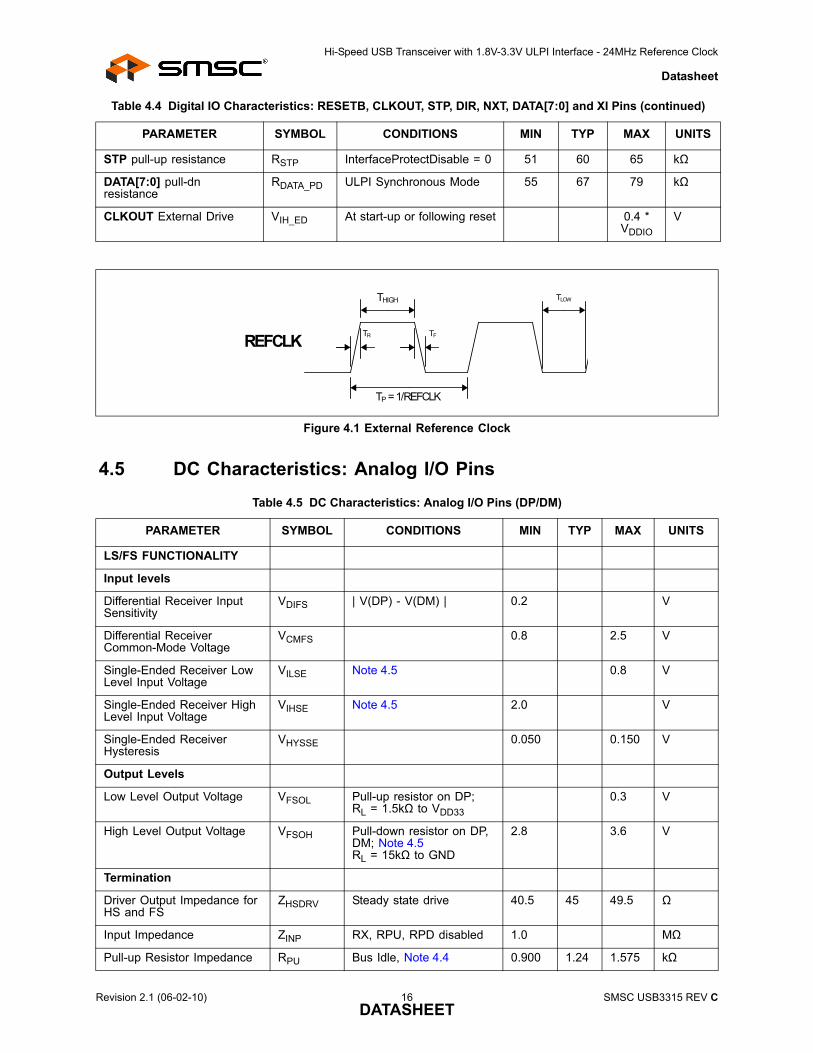
4.5 DC Characteristics: Analog I/O Pins
STP pull-up resistance RSTP InterfaceProtectDisable = 0 51 60 65 kΩ
DATA[7:0] pull-dn resistance
RDATA_PD ULPI Synchronous Mode 55 67 79 kΩ
CLKOUT External Drive VIH_ED At start-up or following reset 0.4 *VDDIO
V
Figure 4.1 External Reference Clock
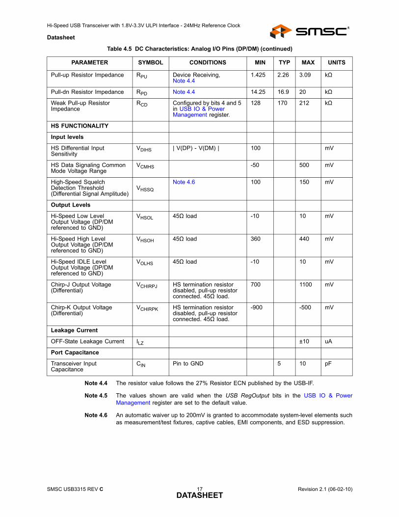
Table 4.5 DC Characteristics: Analog I/O Pins (DP/DM)
PARAMETER SYMBOL CONDITIONS MIN TYP MAX UNITS
LS/FS FUNCTIONALITY
Input levels
Differential Receiver Input Sensitivity
VDIFS | V(DP) - V(DM) | 0.2 V
Differential ReceiverCommon-Mode Voltage
VCMFS 0.8 2.5 V
Single-Ended Receiver Low Level Input Voltage
VILSE Note 4.5 0.8 V
Single-Ended Receiver High Level Input Voltage
VIHSE Note 4.5 2.0 V
Single-Ended Receiver Hysteresis
VHYSSE 0.050 0.150 V
Output Levels
Low Level Output Voltage VFSOL Pull-up resistor on DP;RL = 1.5kΩ to VDD33
0.3 V
High Level Output Voltage VFSOH Pull-down resistor on DP, DM; Note 4.5RL = 15kΩ to GND
2.8 3.6 V
Termination
Driver Output Impedance forHS and FS
ZHSDRV Steady state drive 40.5 45 49.5 Ω
Input Impedance ZINP RX, RPU, RPD disabled 1.0 MΩ
Pull-up Resistor Impedance RPU Bus Idle, Note 4.4 0.900 1.24 1.575 kΩ
Table 4.4 Digital IO Characteristics: RESETB, CLKOUT, STP, DIR, NXT, DATA[7:0] and XI Pins (continued)
PARAMETER SYMBOL CONDITIONS MIN TYP MAX UNITS
TR TF
TLOW
TP = 1/REFCLK
THIGH
REFCLK
Revision 2.1 (06-02-10) 16 SMSC USB3315 REV CDATASHEET
Hi-Speed USB Transceiver with 1.8V-3.3V ULPI Interface - 24MHz Reference Clock
Datasheet
Note 4.4 The resistor value follows the 27% Resistor ECN published by the USB-IF.
Note 4.5 The values shown are valid when the USB RegOutput bits in the USB IO & PowerManagement register are set to the default value.
Note 4.6 An automatic waiver up to 200mV is granted to accommodate system-level elements suchas measurement/test fixtures, captive cables, EMI components, and ESD suppression.
Pull-up Resistor Impedance RPU Device Receiving, Note 4.4
1.425 2.26 3.09 kΩ
Pull-dn Resistor Impedance RPD Note 4.4 14.25 16.9 20 kΩ
Weak Pull-up Resistor Impedance
RCD Configured by bits 4 and 5 in USB IO & Power Management register.
128 170 212 kΩ
HS FUNCTIONALITY
Input levels
HS Differential Input Sensitivity
VDIHS | V(DP) - V(DM) | 100 mV
HS Data Signaling CommonMode Voltage Range
VCMHS -50 500 mV
High-Speed Squelch Detection Threshold (Differential Signal Amplitude)
VHSSQNote 4.6 100 150 mV
Output Levels
Hi-Speed Low LevelOutput Voltage (DP/DMreferenced to GND)
VHSOL 45Ω load -10 10 mV
Hi-Speed High LevelOutput Voltage (DP/DMreferenced to GND)
VHSOH 45Ω load 360 440 mV
Hi-Speed IDLE LevelOutput Voltage (DP/DMreferenced to GND)
VOLHS 45Ω load -10 10 mV
Chirp-J Output Voltage (Differential)
VCHIRPJ HS termination resistor disabled, pull-up resistor connected. 45Ω load.
700 1100 mV
Chirp-K Output Voltage(Differential)
VCHIRPK HS termination resistor disabled, pull-up resistor connected. 45Ω load.
-900 -500 mV
Leakage Current
OFF-State Leakage Current ILZ ±10 uA
Port Capacitance
Transceiver Input Capacitance
CIN Pin to GND 5 10 pF
Table 4.5 DC Characteristics: Analog I/O Pins (DP/DM) (continued)
PARAMETER SYMBOL CONDITIONS MIN TYP MAX UNITS
SMSC USB3315 REV C 17 Revision 2.1 (06-02-10)DATASHEET
Hi-Speed USB Transceiver with 1.8V-3.3V ULPI Interface - 24MHz Reference Clock
Datasheet
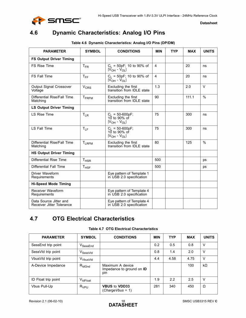
4.6 Dynamic Characteristics: Analog I/O Pins
4.7 OTG Electrical Characteristics
Table 4.6 Dynamic Characteristics: Analog I/O Pins (DP/DM)
PARAMETER SYMBOL CONDITIONS MIN TYP MAX UNITS
FS Output Driver Timing
FS Rise Time TFR CL = 50pF; 10 to 90% of|VOH - VOL|
4 20 ns
FS Fall Time TFF CL = 50pF; 10 to 90% of|VOH - VOL|
4 20 ns
Output Signal Crossover Voltage
VCRS Excluding the first transition from IDLE state
1.3 2.0 V
Differential Rise/Fall Time Matching
TFRFM Excluding the first transition from IDLE state
90 111.1 %
LS Output Driver Timing
LS Rise Time TLR CL = 50-600pF;10 to 90% of|VOH - VOL|
75 300 ns
LS Fall Time TLF CL = 50-600pF;10 to 90% of|VOH - VOL|
75 300 ns
Differential Rise/Fall Time Matching
TLRFM Excluding the first transition from IDLE state
80 125 %
HS Output Driver Timing
Differential Rise Time THSR 500 ps
Differential Fall Time THSF 500 ps
Driver Waveform Requirements
Eye pattern of Template 1 in USB 2.0 specification
Hi-Speed Mode Timing
Receiver Waveform Requirements
Eye pattern of Template 4 in USB 2.0 specification
Data Source Jitter and Receiver Jitter Tolerance
Eye pattern of Template 4 in USB 2.0 specification
Table 4.7 OTG Electrical Characteristics
PARAMETER SYMBOL CONDITIONS MIN TYP MAX UNITS
SessEnd trip point VSessEnd 0.2 0.5 0.8 V
SessVld trip point VSessVld 0.8 1.4 2.0 V
VbusVld trip point VVbusVld 4.4 4.58 4.75 V
A-Device Impedance RIdGnd Maximum A device Impedance to ground on ID pin
100 kΩ
ID Float trip point VIdFloat 1.9 2.2 2.5 V
Vbus Pull-Up RVPU VBUS to VDD33 (ChargeVbus = 1)
281 340 450 Ω
Revision 2.1 (06-02-10) 18 SMSC USB3315 REV CDATASHEET
Hi-Speed USB Transceiver with 1.8V-3.3V ULPI Interface - 24MHz Reference Clock
Datasheet
4.8 Regulator Output Voltages and Capacitor Requirement
Note 4.7 REFCLK pin ±5kV Human Body Model.
Vbus Pull-down RVPD VBUS to GND (DisChargeVbus = 1)
656 850 1100 Ω
Vbus Impedance RVB VBUS to GND 40 75 100 kΩ
ID pull-up resistance RID IdPullup = 1 80 100 120 kΩ
ID weak pull-up resistance RIDW IdPullup = 0 1 MΩ
ID pull-dn resistance RIDPD IdGndDrv = 1 1000 Ω
Table 4.8 Regulator Output Voltages and Capacitor Requirement
PARAMETER SYMBOL CONDITIONS MIN TYP MAX UNITS
Regulator Output Voltage VDD33 6V > VBAT > 3.1V 3.0 3.3 3.6 V
Regulator Output Voltage VDD33 USB UART Mode & UART RegOutput[1:0] = 016V > VBAT > 3.1V
2.7 3.0 3.3 V
Regulator Output Voltage VDD33 USB UART Mode & UART RegOutput[1:0] = 106V > VBAT > 3.1V
2.47 2.75 3.03 V
Regulator Output Voltage VDD33 USB UART Mode & UART RegOutput[1:0] = 116V > VBAT > 3.1V
2.25 2.5 2.75 V
Regulator Bypass Capacitor CBYP 2.2 uF
Bypass Capacitor ESR CESR 1 Ω
Table 4.9 ESD and LATCH-UP Performance
PARAMETER CONDITIONS MIN TYP MAX UNITS COMMENTS
ESD PERFORMANCE
Note 4.7 Human Body Model ±8 kV Device
System EN/IEC 61000-4-2 Contact Discharge
±8 kV 3rd party system test
System EN/IEC 61000-4-2 Air-gap Discharge
±15 kV 3rd party system test
LATCH-UP PERFORMANCE
All Pins EIA/JESD 78, Class II 150 mA
Table 4.7 OTG Electrical Characteristics (continued)
PARAMETER SYMBOL CONDITIONS MIN TYP MAX UNITS
SMSC USB3315 REV C 19 Revision 2.1 (06-02-10)DATASHEET
Hi-Speed USB Transceiver with 1.8V-3.3V ULPI Interface - 24MHz Reference Clock
Datasheet
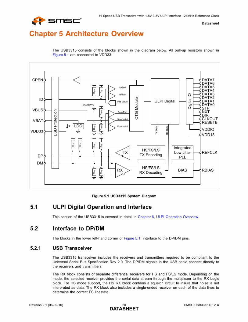
Chapter 5 Architecture Overview
The USB3315 consists of the blocks shown in the diagram below. All pull-up resistors shown inFigure 5.1 are connected to VDD33.
Figure 5.1 USB3315 System Diagram
5.1 ULPI Digital Operation and InterfaceThis section of the USB3315 is covered in detail in Chapter 6, ULPI Operation Overview.
5.2 Interface to DP/DMThe blocks in the lower left-hand corner of Figure 5.1 interface to the DP/DM pins.
5.2.1 USB Transceiver
The USB3315 transceiver includes the receivers and transmitters required to be compliant to theUniversal Serial Bus Specification Rev 2.0. The DP/DM signals in the USB cable connect directly tothe receivers and transmitters.
The RX block consists of separate differential receivers for HS and FS/LS mode. Depending on themode, the selected receiver provides the serial data stream through the multiplexer to the RX Logicblock. For HS mode support, the HS RX block contains a squelch circuit to insure that noise is notinterpreted as data. The RX block also includes a single-ended receiver on each of the data lines todetermine the correct FS linestate.
BIAS
Integrated Low Jitter
PLL
RBIAS
ES
D P
rote
ctio
n
RC
D
RC
D
RP
D
RP
D
RP
U
RP
UR
ID
RID
W
RVP
UR
VP
D
RV
B
DIRNXTSTP
CLKOUT
DATA7DATA6DATA5DATA4DATA3DATA2
DATA0DATA1
REFCLK
VDDIO
VBAT
VDD33
VBUS
LDO
DP
DM
ID ULPI Digital
Dig
ital I
O
OTG
Mod
ule
TX
RX
HS/FS/LSTX Encoding
HS/FS/LSRX Decoding
RESETB
TX D
ata
RX
Dat
a
IdGnd
IdFloat
Rid Value
SessEnd
SessValid
VbusValid
VDD18
IdGndDrv
CPEN
Revision 2.1 (06-02-10) 20 SMSC USB3315 REV CDATASHEET
Hi-Speed USB Transceiver with 1.8V-3.3V ULPI Interface - 24MHz Reference Clock
Datasheet
Data from the TX Logic block is encoded, bit stuffed, serialized and transmitted onto the USB cableby the TX block. Separate differential FS/LS and HS transmitters are included to support all modes.
The USB3315 TX block meets the HS signalling level requirements in the USB 2.0 Specification whenthe PCB traces from the DP and DM pins to the USB connector have very little loss. In some systems,it may be desirable to compensate for loss by adjusting the HS transmitter amplitude. The Boost bitsin the HS TX Boost register may be configured to adjust the HS transmitter amplitude at the DP andDM pins.
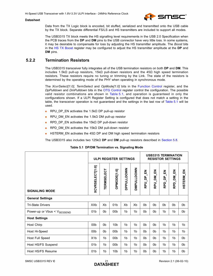
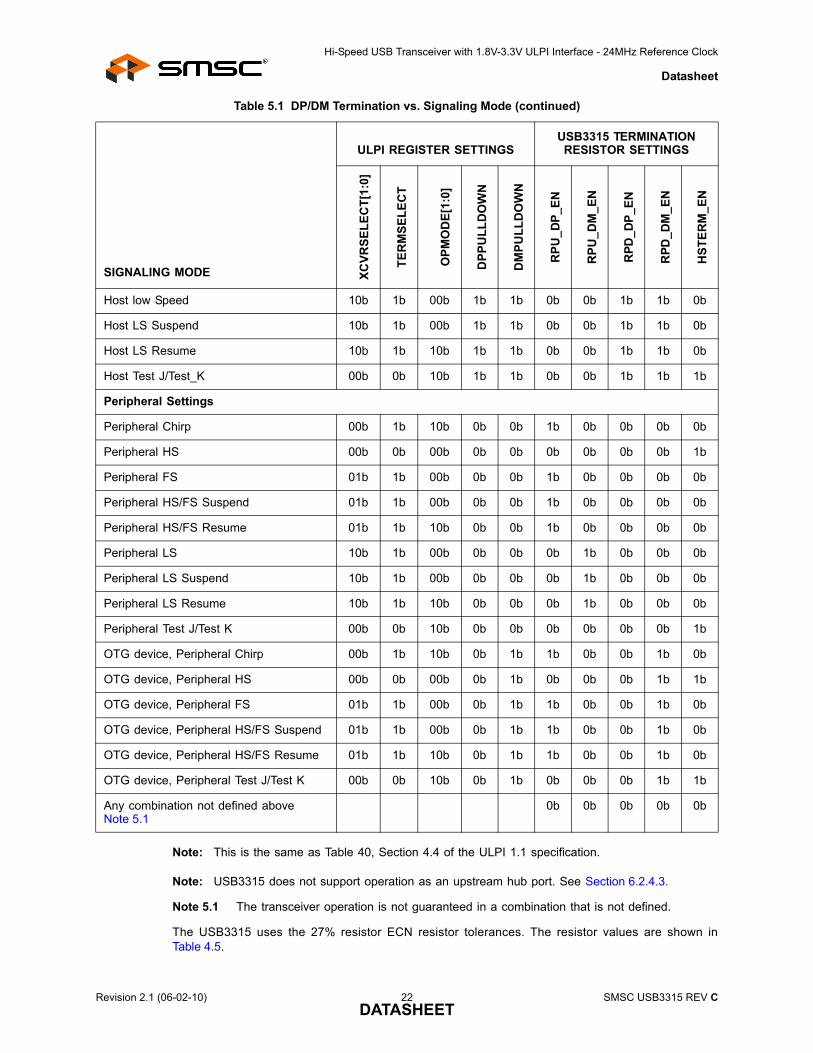
5.2.2 Termination Resistors
The USB3315 transceiver fully integrates all of the USB termination resistors on both DP and DM. Thisincludes 1.5kΩ pull-up resistors, 15kΩ pull-down resistors and the 45Ω high speed terminationresistors. These resistors require no tuning or trimming by the Link. The state of the resistors isdetermined by the operating mode of the PHY when operating in synchronous mode.
The XcvrSelect[1:0], TermSelect and OpMode[1:0] bits in the Function Control register, and theDpPulldown and DmPulldown bits in the OTG Control register control the configuration. The possiblevalid resistor combinations are shown in Table 5.1, and operation is guaranteed in only theconfigurations shown. If a ULPI Register Setting is configured that does not match a setting in thetable, the transceiver operation is not guaranteed and the settings in the last row of Table 5.1 will beused.
RPU_DP_EN activates the 1.5kΩ DP pull-up resistor
RPU_DM_EN activates the 1.5kΩ DM pull-up resistor
RPD_DP_EN activates the 15kΩ DP pull-down resistor
RPD_DM_EN activates the 15kΩ DM pull-down resistor
HSTERM_EN activates the 45Ω DP and DM high speed termination resistors
The USB3315 also includes two 125kΩ DP and DM pull-up resistors described in Section 5.8.
Table 5.1 DP/DM Termination vs. Signaling Mode
SIGNALING MODE
ULPI REGISTER SETTINGSUSB3315 TERMINATION RESISTOR SETTINGS
XCVR
SELE
CT[
1:0]
TER
MSE
LEC
T
OPM
OD
E[1:
0]
DPP
ULL
DO
WN
DM
PULL
DO
WN
RPU
_DP_
EN
RPU
_DM
_EN
RPD
_DP_
EN
RPD
_DM
_EN
HST
ERM
_EN
General Settings
Tri-State Drivers XXb Xb 01b Xb Xb 0b 0b 0b 0b 0b
Power-up or Vbus < VSESSEND 01b 0b 00b 1b 1b 0b 0b 1b 1b 0b
Host Settings
Host Chirp 00b 0b 10b 1b 1b 0b 0b 1b 1b 1b
Host Hi-Speed 00b 0b 00b 1b 1b 0b 0b 1b 1b 1b
Host Full Speed X1b 1b 00b 1b 1b 0b 0b 1b 1b 0b
Host HS/FS Suspend 01b 1b 00b 1b 1b 0b 0b 1b 1b 0b
Host HS/FS Resume 01b 1b 10b 1b 1b 0b 0b 1b 1b 0b
SMSC USB3315 REV C 21 Revision 2.1 (06-02-10)DATASHEET
Hi-Speed USB Transceiver with 1.8V-3.3V ULPI Interface - 24MHz Reference Clock
Datasheet
Note: This is the same as Table 40, Section 4.4 of the ULPI 1.1 specification.
Note: USB3315 does not support operation as an upstream hub port. See Section 6.2.4.3.
Note 5.1 The transceiver operation is not guaranteed in a combination that is not defined.
The USB3315 uses the 27% resistor ECN resistor tolerances. The resistor values are shown inTable 4.5.
Host low Speed 10b 1b 00b 1b 1b 0b 0b 1b 1b 0b
Host LS Suspend 10b 1b 00b 1b 1b 0b 0b 1b 1b 0b
Host LS Resume 10b 1b 10b 1b 1b 0b 0b 1b 1b 0b
Host Test J/Test_K 00b 0b 10b 1b 1b 0b 0b 1b 1b 1b
Peripheral Settings
Peripheral Chirp 00b 1b 10b 0b 0b 1b 0b 0b 0b 0b
Peripheral HS 00b 0b 00b 0b 0b 0b 0b 0b 0b 1b
Peripheral FS 01b 1b 00b 0b 0b 1b 0b 0b 0b 0b
Peripheral HS/FS Suspend 01b 1b 00b 0b 0b 1b 0b 0b 0b 0b
Peripheral HS/FS Resume 01b 1b 10b 0b 0b 1b 0b 0b 0b 0b
Peripheral LS 10b 1b 00b 0b 0b 0b 1b 0b 0b 0b
Peripheral LS Suspend 10b 1b 00b 0b 0b 0b 1b 0b 0b 0b
Peripheral LS Resume 10b 1b 10b 0b 0b 0b 1b 0b 0b 0b
Peripheral Test J/Test K 00b 0b 10b 0b 0b 0b 0b 0b 0b 1b
OTG device, Peripheral Chirp 00b 1b 10b 0b 1b 1b 0b 0b 1b 0b
OTG device, Peripheral HS 00b 0b 00b 0b 1b 0b 0b 0b 1b 1b
OTG device, Peripheral FS 01b 1b 00b 0b 1b 1b 0b 0b 1b 0b
OTG device, Peripheral HS/FS Suspend 01b 1b 00b 0b 1b 1b 0b 0b 1b 0b
OTG device, Peripheral HS/FS Resume 01b 1b 10b 0b 1b 1b 0b 0b 1b 0b
OTG device, Peripheral Test J/Test K 00b 0b 10b 0b 1b 0b 0b 0b 1b 1b
Any combination not defined aboveNote 5.1
0b 0b 0b 0b 0b
Table 5.1 DP/DM Termination vs. Signaling Mode (continued)
SIGNALING MODE
ULPI REGISTER SETTINGSUSB3315 TERMINATION RESISTOR SETTINGS
XCVR
SELE
CT[
1:0]
TER
MSE
LEC
T
OPM
OD
E[1:
0]
DPP
ULL
DO
WN
DM
PULL
DO
WN
RPU
_DP_
EN
RPU
_DM
_EN
RPD
_DP_
EN
RPD
_DM
_EN
HST
ERM
_EN
Revision 2.1 (06-02-10) 22 SMSC USB3315 REV CDATASHEET
Hi-Speed USB Transceiver with 1.8V-3.3V ULPI Interface - 24MHz Reference Clock
Datasheet
5.3 Bias GeneratorThis block consists of an internal bandgap reference circuit used for generating the driver current andthe biasing of the analog circuits. This block requires an external 8.06KΩ, 1% tolerance, referenceresistor connected from RBIAS to ground. This resistor should be placed as close as possible to theUSB3315 to minimize the trace length. The nominal voltage at RBIAS is 0.8V and therefore the resistorwill dissipate approximately 80μW of power.
5.4 Integrated Low Jitter PLLThe USB3315 uses an integrated low jitter phase locked loop (PLL) to provide a clean 480MHz clock.This clock is used by the PHY during both transmit and receive. The USB3315 requires a 24MHzreference clock to be driven on the REFCLK pin.
After the PLL has locked to the correct frequency, the USB3315 will de-assert DIR and the Link canbegin using the ULPI interface. The USB3315 is guaranteed to start the clock within the time specifiedin Table 4.2. For Host applications, the ULPI AutoResume bit should be enabled. This is described inSection 6.2.4.4.
The system must not drive voltage on the CLKOUT pin following POR or hardware reset that exceedsthe value of VIH_ED provided in Table 4.4.
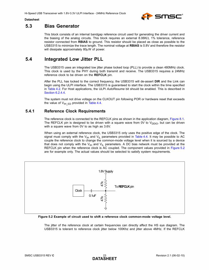
5.4.1 Reference Clock Requirements
The reference clock is connected to the REFCLK pins as shown in the application diagram, Figure 8.1.The REFCLK pin is designed to be driven with a square wave from 0V to VDDIO, but can be drivenwith a square wave from 0V to as high as 3.6V.
When using an external reference clock, the USB3315 only uses the positive edge of the clock. Thesignal must comply with the VIH and VIL parameters provided in Table 4.4. It may be possible to ACcouple the reference clock to change the common-mode voltage level when it is sourced by a devicethat does not comply with the VIH and VIL parameters. A DC bias network must be provided at theREFCLK pin when the reference clock is AC coupled. The component values provided in Figure 5.2are for example only. The actual values should be selected to satisfy system requirements.
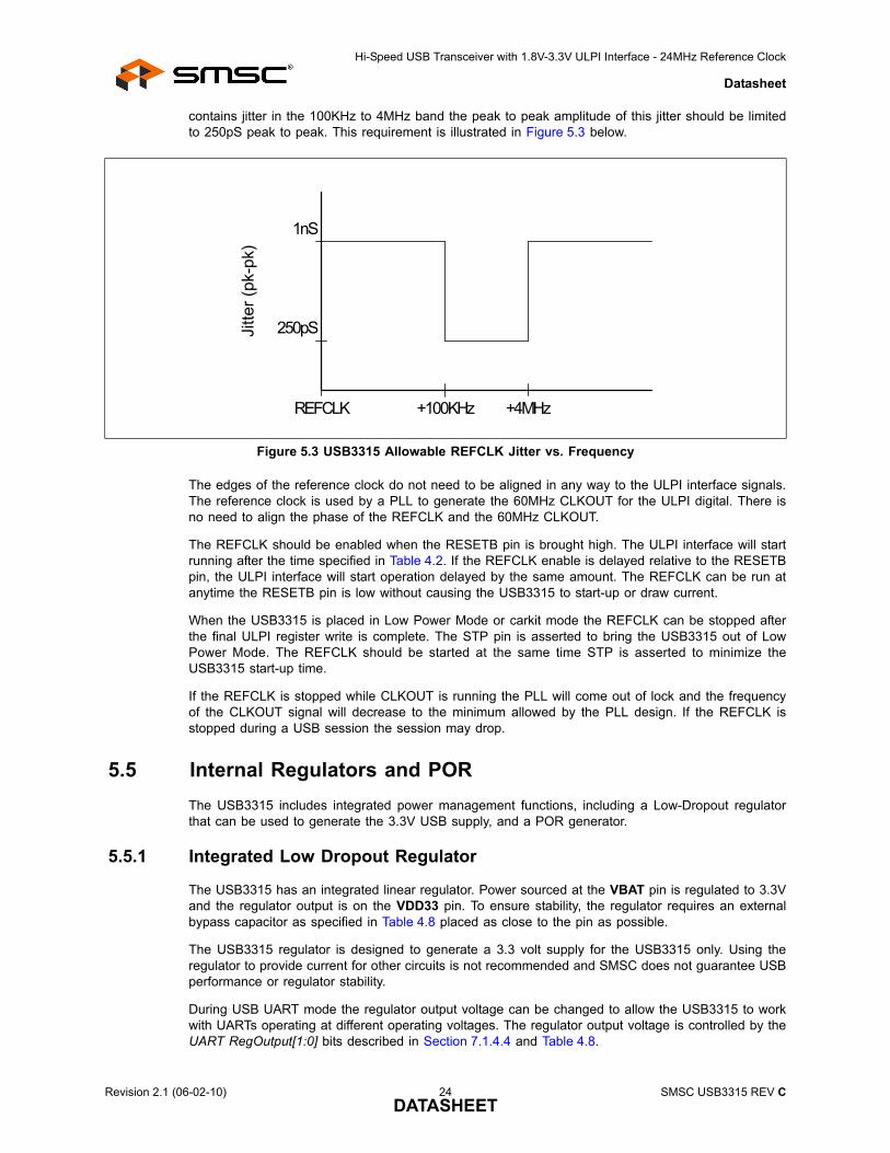
The jitter of the reference clock at certain frequencies can directly affect the HS eye diagram. TheUSB3315 is tolerant to reference clock jitter below 100Khz and jitter above 4MHz. If the REFCLK
Figure 5.2 Example of circuit used to shift a reference clock common-mode voltage level.
Clock
47k
47k
0.1uF
1.8V Supply
To REFCLK pin
SMSC USB3315 REV C 23 Revision 2.1 (06-02-10)DATASHEET
Hi-Speed USB Transceiver with 1.8V-3.3V ULPI Interface - 24MHz Reference Clock
Datasheet
contains jitter in the 100KHz to 4MHz band the peak to peak amplitude of this jitter should be limitedto 250pS peak to peak. This requirement is illustrated in Figure 5.3 below.
The edges of the reference clock do not need to be aligned in any way to the ULPI interface signals.The reference clock is used by a PLL to generate the 60MHz CLKOUT for the ULPI digital. There isno need to align the phase of the REFCLK and the 60MHz CLKOUT.
The REFCLK should be enabled when the RESETB pin is brought high. The ULPI interface will startrunning after the time specified in Table 4.2. If the REFCLK enable is delayed relative to the RESETBpin, the ULPI interface will start operation delayed by the same amount. The REFCLK can be run atanytime the RESETB pin is low without causing the USB3315 to start-up or draw current.
When the USB3315 is placed in Low Power Mode or carkit mode the REFCLK can be stopped afterthe final ULPI register write is complete. The STP pin is asserted to bring the USB3315 out of LowPower Mode. The REFCLK should be started at the same time STP is asserted to minimize theUSB3315 start-up time.
If the REFCLK is stopped while CLKOUT is running the PLL will come out of lock and the frequencyof the CLKOUT signal will decrease to the minimum allowed by the PLL design. If the REFCLK isstopped during a USB session the session may drop.
5.5 Internal Regulators and PORThe USB3315 includes integrated power management functions, including a Low-Dropout regulatorthat can be used to generate the 3.3V USB supply, and a POR generator.
5.5.1 Integrated Low Dropout Regulator
The USB3315 has an integrated linear regulator. Power sourced at the VBAT pin is regulated to 3.3Vand the regulator output is on the VDD33 pin. To ensure stability, the regulator requires an externalbypass capacitor as specified in Table 4.8 placed as close to the pin as possible.
The USB3315 regulator is designed to generate a 3.3 volt supply for the USB3315 only. Using theregulator to provide current for other circuits is not recommended and SMSC does not guarantee USBperformance or regulator stability.
During USB UART mode the regulator output voltage can be changed to allow the USB3315 to workwith UARTs operating at different operating voltages. The regulator output voltage is controlled by theUART RegOutput[1:0] bits described in Section 7.1.4.4 and Table 4.8.
Figure 5.3 USB3315 Allowable REFCLK Jitter vs. Frequency
Jitte
r (pk
-pk)
1nS
250pS
+100KHz +4MHzREFCLK
Revision 2.1 (06-02-10) 24 SMSC USB3315 REV CDATASHEET
Hi-Speed USB Transceiver with 1.8V-3.3V ULPI Interface - 24MHz Reference Clock
Datasheet
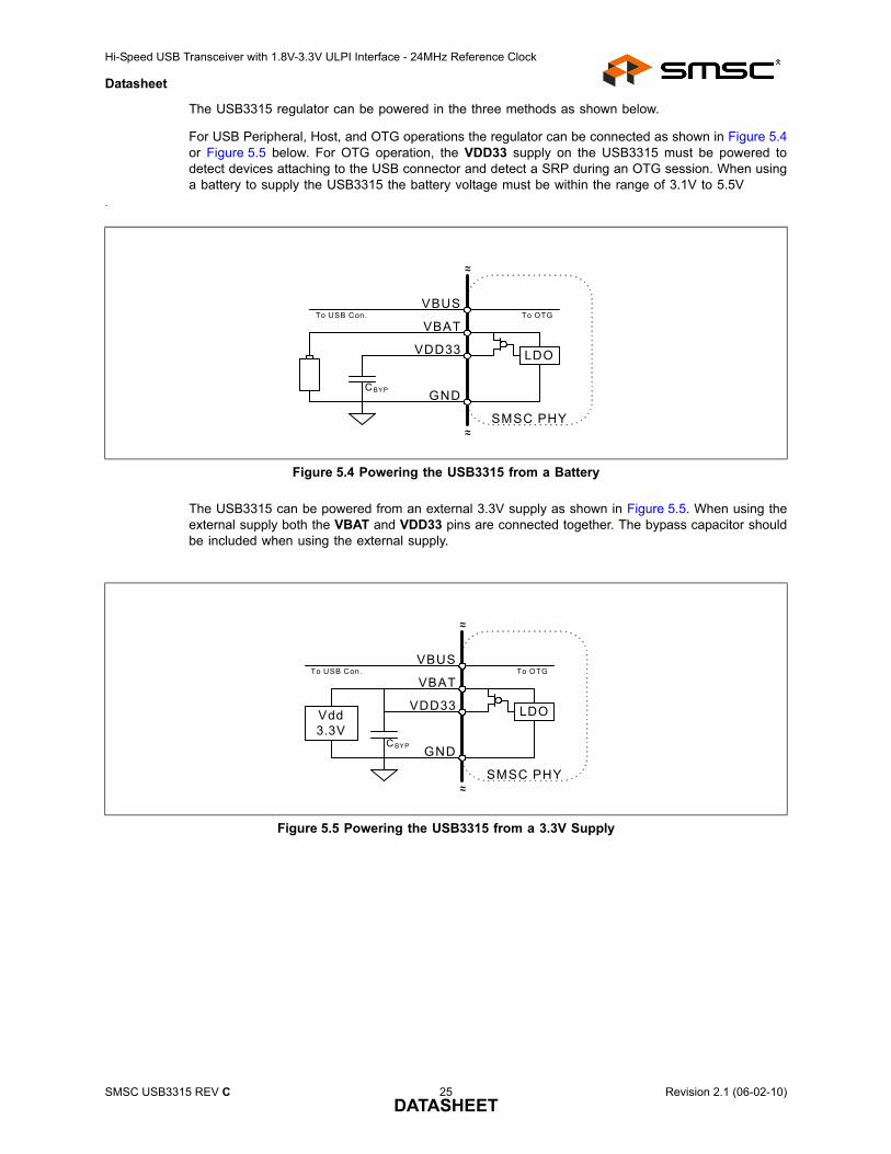
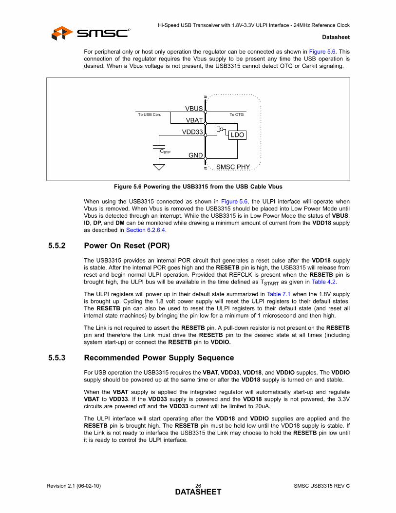
The USB3315 regulator can be powered in the three methods as shown below.
For USB Peripheral, Host, and OTG operations the regulator can be connected as shown in Figure 5.4or Figure 5.5 below. For OTG operation, the VDD33 supply on the USB3315 must be powered todetect devices attaching to the USB connector and detect a SRP during an OTG session. When usinga battery to supply the USB3315 the battery voltage must be within the range of 3.1V to 5.5V
.
The USB3315 can be powered from an external 3.3V supply as shown in Figure 5.5. When using theexternal supply both the VBAT and VDD33 pins are connected together. The bypass capacitor shouldbe included when using the external supply.
Figure 5.4 Powering the USB3315 from a Battery
Figure 5.5 Powering the USB3315 from a 3.3V Supply
VBUS
VDD33
VBAT
GND
LDO
~~
~~
To USB Con.
SMSC PHY
To OTG
CBYP
VBUS
VDD33
VBAT
GND
LDO
~~
~~
To USB Con.
SMSC PHY
To OTG
CBYP
Vdd 3.3V
SMSC USB3315 REV C 25 Revision 2.1 (06-02-10)DATASHEET
Hi-Speed USB Transceiver with 1.8V-3.3V ULPI Interface - 24MHz Reference Clock
Datasheet
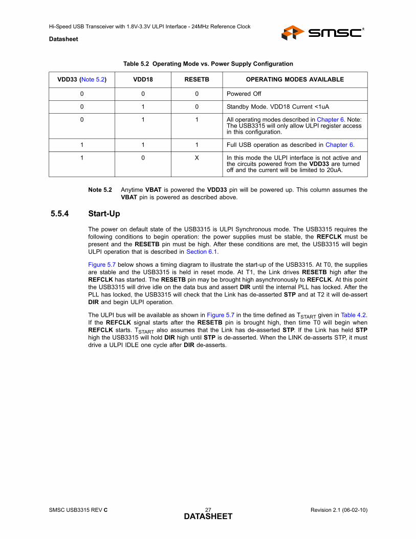
For peripheral only or host only operation the regulator can be connected as shown in Figure 5.6. Thisconnection of the regulator requires the Vbus supply to be present any time the USB operation isdesired. When a Vbus voltage is not present, the USB3315 cannot detect OTG or Carkit signaling.
When using the USB3315 connected as shown in Figure 5.6, the ULPI interface will operate whenVbus is removed. When Vbus is removed the USB3315 should be placed into Low Power Mode untilVbus is detected through an interrupt. While the USB3315 is in Low Power Mode the status of VBUS,ID, DP, and DM can be monitored while drawing a minimum amount of current from the VDD18 supplyas described in Section 6.2.6.4.
5.5.2 Power On Reset (POR)
The USB3315 provides an internal POR circuit that generates a reset pulse after the VDD18 supplyis stable. After the internal POR goes high and the RESETB pin is high, the USB3315 will release fromreset and begin normal ULPI operation. Provided that REFCLK is present when the RESETB pin isbrought high, the ULPI bus will be available in the time defined as TSTART as given in Table 4.2.
The ULPI registers will power up in their default state summarized in Table 7.1 when the 1.8V supplyis brought up. Cycling the 1.8 volt power supply will reset the ULPI registers to their default states.The RESETB pin can also be used to reset the ULPI registers to their default state (and reset allinternal state machines) by bringing the pin low for a minimum of 1 microsecond and then high.
The Link is not required to assert the RESETB pin. A pull-down resistor is not present on the RESETBpin and therefore the Link must drive the RESETB pin to the desired state at all times (includingsystem start-up) or connect the RESETB pin to VDDIO.
5.5.3 Recommended Power Supply Sequence
For USB operation the USB3315 requires the VBAT, VDD33, VDD18, and VDDIO supples. The VDDIOsupply should be powered up at the same time or after the VDD18 supply is turned on and stable.
When the VBAT supply is applied the integrated regulator will automatically start-up and regulateVBAT to VDD33. If the VDD33 supply is powered and the VDD18 supply is not powered, the 3.3Vcircuits are powered off and the VDD33 current will be limited to 20uA.
The ULPI interface will start operating after the VDD18 and VDDIO supplies are applied and theRESETB pin is brought high. The RESETB pin must be held low until the VDD18 supply is stable. Ifthe Link is not ready to interface the USB3315 the Link may choose to hold the RESETB pin low untilit is ready to control the ULPI interface.
Figure 5.6 Powering the USB3315 from the USB Cable Vbus
VBUS
VDD33
VBAT
GND
LDO
~~
~~
To USB Con.
SMSC PHY
To OTG
CBYP
Revision 2.1 (06-02-10) 26 SMSC USB3315 REV CDATASHEET
Hi-Speed USB Transceiver with 1.8V-3.3V ULPI Interface - 24MHz Reference Clock
Datasheet
Note 5.2 Anytime VBAT is powered the VDD33 pin will be powered up. This column assumes theVBAT pin is powered as described above.
5.5.4 Start-Up
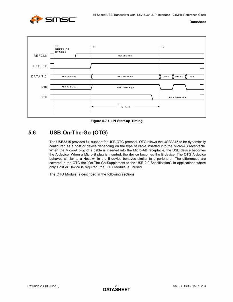
The power on default state of the USB3315 is ULPI Synchronous mode. The USB3315 requires thefollowing conditions to begin operation: the power supplies must be stable, the REFCLK must bepresent and the RESETB pin must be high. After these conditions are met, the USB3315 will beginULPI operation that is described in Section 6.1.
Figure 5.7 below shows a timing diagram to illustrate the start-up of the USB3315. At T0, the suppliesare stable and the USB3315 is held in reset mode. At T1, the Link drives RESETB high after theREFCLK has started. The RESETB pin may be brought high asynchronously to REFCLK. At this pointthe USB3315 will drive idle on the data bus and assert DIR until the internal PLL has locked. After thePLL has locked, the USB3315 will check that the Link has de-asserted STP and at T2 it will de-assertDIR and begin ULPI operation.
The ULPI bus will be available as shown in Figure 5.7 in the time defined as TSTART given in Table 4.2.If the REFCLK signal starts after the RESETB pin is brought high, then time T0 will begin whenREFCLK starts. TSTART also assumes that the Link has de-asserted STP. If the Link has held STPhigh the USB3315 will hold DIR high until STP is de-asserted. When the LINK de-asserts STP, it mustdrive a ULPI IDLE one cycle after DIR de-asserts.
Table 5.2 Operating Mode vs. Power Supply Configuration
VDD33 (Note 5.2) VDD18 RESETB OPERATING MODES AVAILABLE
0 0 0 Powered Off
0 1 0 Standby Mode. VDD18 Current <1uA
0 1 1 All operating modes described in Chapter 6. Note: The USB3315 will only allow ULPI register access in this configuration.
1 1 1 Full USB operation as described in Chapter 6.
1 0 X In this mode the ULPI interface is not active and the circuits powered from the VDD33 are turned off and the current will be limited to 20uA.
SMSC USB3315 REV C 27 Revision 2.1 (06-02-10)DATASHEET
Hi-Speed USB Transceiver with 1.8V-3.3V ULPI Interface - 24MHz Reference Clock
Datasheet
5.6 USB On-The-Go (OTG)The USB3315 provides full support for USB OTG protocol. OTG allows the USB3315 to be dynamicallyconfigured as a host or device depending on the type of cable inserted into the Micro-AB receptacle.When the Micro-A plug of a cable is inserted into the Micro-AB receptacle, the USB device becomesthe A-device. When a Micro-B plug is inserted, the device becomes the B-device. The OTG A-devicebehaves similar to a Host while the B-device behaves similar to a peripheral. The differences arecovered in the OTG the “On-The-Go Supplement to the USB 2.0 Specification”. In applications whereonly Host or Device is required, the OTG Module is unused.
The OTG Module is described in the following sections.
Figure 5.7 ULPI Start-up Timing
D IR
R E S E T B
S T P
T S T A R T
R E F C LK
T 1 T 2T 0S U P P L IE S S T A B L E
P H Y D rives Id leD A T A [7 :0 ]
R E F C L K va lid
P H Y T ri-S ta tes
P H Y T ri-S ta tes P H Y D rives H ig h
L IN K D rives L o w
R X C M DID L E ID L E
Revision 2.1 (06-02-10) 28 SMSC USB3315 REV CDATASHEET
Hi-Speed USB Transceiver with 1.8V-3.3V ULPI Interface - 24MHz Reference Clock
Datasheet
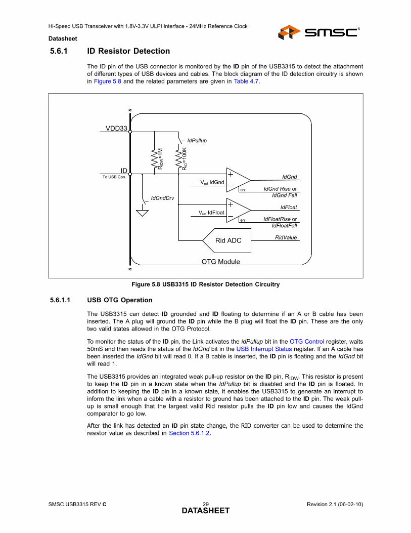
5.6.1 ID Resistor Detection
The ID pin of the USB connector is monitored by the ID pin of the USB3315 to detect the attachmentof different types of USB devices and cables. The block diagram of the ID detection circuitry is shownin Figure 5.8 and the related parameters are given in Table 4.7.
5.6.1.1 USB OTG Operation
The USB3315 can detect ID grounded and ID floating to determine if an A or B cable has beeninserted. The A plug will ground the ID pin while the B plug will float the ID pin. These are the onlytwo valid states allowed in the OTG Protocol.
To monitor the status of the ID pin, the Link activates the idPullup bit in the OTG Control register, waits50mS and then reads the status of the IdGnd bit in the USB Interrupt Status register. If an A cable hasbeen inserted the IdGnd bit will read 0. If a B cable is inserted, the ID pin is floating and the IdGnd bitwill read 1.
The USB3315 provides an integrated weak pull-up resistor on the ID pin, RIDW. This resistor is presentto keep the ID pin in a known state when the IdPullup bit is disabled and the ID pin is floated. Inaddition to keeping the ID pin in a known state, it enables the USB3315 to generate an interrupt toinform the link when a cable with a resistor to ground has been attached to the ID pin. The weak pull-up is small enough that the largest valid Rid resistor pulls the ID pin low and causes the IdGndcomparator to go low.
After the link has detected an ID pin state change, the RID converter can be used to determine theresistor value as described in Section 5.6.1.2.
Figure 5.8 USB3315 ID Resistor Detection Circuitry
IdPullup
IdGndVref IdGnd
RID
=100
K
RID
W>1
M
IdFloat
ID
~~
~~ OTG Module
VDD33
To USB Con.
RidValue
Vref IdFloat
IdGnd Rise orIdGnd Fall
IdFloatRise orIdFloatFall
Rid ADC
IdGndDrven
en
SMSC USB3315 REV C 29 Revision 2.1 (06-02-10)DATASHEET
Hi-Speed USB Transceiver with 1.8V-3.3V ULPI Interface - 24MHz Reference Clock
Datasheet
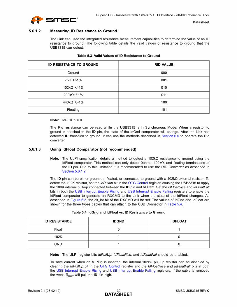
5.6.1.2 Measuring ID Resistance to Ground
The Link can used the integrated resistance measurement capabilities to determine the value of an IDresistance to ground. The following table details the valid values of resistance to ground that theUSB3315 can detect.
Note: IdPullUp = 0
The Rid resistance can be read while the USB3315 is in Synchronous Mode. When a resistor toground is attached to the ID pin, the state of the IdGnd comparator will change. After the Link hasdetected ID transition to ground, it can use the methods described in Section 6.5 to operate the Ridconverter.
5.6.1.3 Using IdFloat Comparator (not recommended)
Note: The ULPI specification details a method to detect a 102kΩ resistance to ground using theIdFloat comparator. This method can only detect 0ohms, 102kΩ, and floating terminations ofthe ID pin. Due to this limitation it is recommended to use the RID Converter as described inSection 5.6.1.2.
The ID pin can be either grounded, floated, or connected to ground with a 102kΩ external resistor. Todetect the 102K resistor, set the idPullup bit in the OTG Control register, causing the USB3315 to applythe 100K internal pull-up connected between the ID pin and VDD33. Set the idFloatRise and idFloatFallbits in both the USB Interrupt Enable Rising and USB Interrupt Enable Falling registers to enable theIdFloat comparator to generate an RXCMD to the Link when the state of the IdFloat changes. Asdescribed in Figure 6.3, the alt_int bit of the RXCMD will be set. The values of IdGnd and IdFloat areshown for the three types cables that can attach to the USB Connector in Table 5.4.
Note: The ULPI register bits IdPullUp, IdFloatRise, and IdFloatFall should be enabled.
To save current when an A Plug is inserted, the internal 102kΩ pull-up resistor can be disabled byclearing the IdPullUp bit in the OTG Control register and the IdFloatRise and IdFloatFall bits in boththe USB Interrupt Enable Rising and USB Interrupt Enable Falling registers. If the cable is removedthe weak RIDW will pull the ID pin high.
Table 5.3 Valid Values of ID Resistance to Ground
ID RESISTANCE TO GROUND RID VALUE
Ground 000
75Ω +/-1% 001
102kΩ +/-1% 010
200kΩ+/-1% 011
440kΩ +/-1% 100
Floating 101
Table 5.4 IdGnd and IdFloat vs. ID Resistance to Ground
ID RESISTANCE IDGND IDFLOAT
Float 0 1
102K 1 0
GND 1 0
Revision 2.1 (06-02-10) 30 SMSC USB3315 REV CDATASHEET
Hi-Speed USB Transceiver with 1.8V-3.3V ULPI Interface - 24MHz Reference Clock
Datasheet
The IdGnd value can be read using the ULPI USB Interrupt Status register, bit 4. In host mode, it canbe set to generate an interrupt when IdGnd changes by setting the appropriate bits in the USB InterruptEnable Rising and USB Interrupt Enable Falling registers. The IdFloat value can be read by readingthe ULPI Carkit Interrupt Status register bit 0.
Note: The IdGnd switch has been provided to ground the ID pin for future applications.
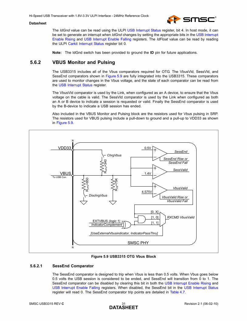
5.6.2 VBUS Monitor and Pulsing
The USB3315 includes all of the Vbus comparators required for OTG. The VbusVld, SessVld, andSessEnd comparators shown in Figure 5.9 are fully integrated into the USB3315. These comparatorsare used to monitor changes in the Vbus voltage, and the state of each comparator can be read fromthe USB Interrupt Status register.
The VbusVld comparator is used by the Link, when configured as an A device, to ensure that the Vbusvoltage on the cable is valid. The SessVld comparator is used by the Link when configured as bothan A or B device to indicate a session is requested or valid. Finally the SessEnd comparator is usedby the B-device to indicate a USB session has ended.
Also included in the VBUS Monitor and Pulsing block are the resistors used for Vbus pulsing in SRP.The resistors used for VBUS pulsing include a pull-down to ground and a pull-up to VDD33 as shownin Figure 5.9.
5.6.2.1 SessEnd Comparator
The SessEnd comparator is designed to trip when Vbus is less than 0.5 volts. When Vbus goes below0.5 volts the USB session is considered to be ended, and SessEnd will transition from 0 to 1. TheSessEnd comparator can be disabled by clearing this bit in both the USB Interrupt Enable Rising andUSB Interrupt Enable Falling registers. When disabled, the SessEnd bit in the USB Interrupt Statusregister will read 0. The SessEnd comparator trip points are detailed in Table 4.7.
Figure 5.9 USB3315 OTG Vbus Block
RVB
=75K
RV
PD=8
50
RV
PU=3
40
VbusValid
SessValid
SessEnd
DischrgVbus
ChrgVbus
0.5V
1.4V
4.575V
VBUS~~
~~
VDD33
SMSC PHY
To USB Con.
SessEnd Rise or SessEnd Fall
VbusValid Rise or VbusValid Fall
RXCMD VbusValid
IndicatorComplement
[UseExternalVbusindicator, IndicatorPassThru]
[0, X]
[1, 0]
[1, 1]EXTVBUS (logic 1)
SMSC USB3315 REV C 31 Revision 2.1 (06-02-10)DATASHEET
Hi-Speed USB Transceiver with 1.8V-3.3V ULPI Interface - 24MHz Reference Clock
Datasheet
5.6.2.2 SessVld Comparator
The SessVld comparator is used when the PHY is configured as both an A and B device. Whenconfigured as an A device, the SessVld is used to detect Session Request protocol (SRP). Whenconfigured as a B device, SessVld is used to detect the presence of Vbus. The SessVld interrupts canbe disabled by clearing this bit in both the USB Interrupt Enable Rising and USB Interrupt EnableFalling registers. When the interrupts are disabled, the SessVld comparator is not disabled and its statecan be read in the USB Interrupt Status register. The SessVld comparator trip point is detailed inTable 4.7.
Note: The OTG Supplement specifies a voltage range for A-Device Session Valid and B-DeviceSession Valid comparator. The USB3315 PHY combines the two comparators into one anduses the narrower threshold range.
5.6.2.3 VbusVld Comparator
The final Vbus comparator is the VbusVld comparator. This comparator is only used when theUSB3315 is configured as an A-device. In the USB protocol the A-device supplies the VBUS voltageand is responsible to ensure it remains within a specified voltage range. The VbusVld comparator canbe disabled by clearing this bit in both the USB Interrupt Enable Rising and USB Interrupt EnableFalling registers. When disabled, bit 1 of the USB Interrupt Status register will return a 0. The VbusVldcomparator trip points are detailed in Table 4.7.
The internal VbusValid comparator is designed to ensure the Vbus voltage remains above 4.4V.
The USB3315 includes the external vbus valid indicator logic as detail in the ULPI Specification. Theexternal vbus valid indicator is tied to a logic one. The decoding of this logic is shown in Table 5.5below. By default this logic is disabled.
Note 5.3 A peripheral should not use VbusVld to begin operation. The peripheral should useSessVld because the internal VbusVld threshold can be above the Vbus voltage requiredfor USB peripheral operation.
Table 5.5 External Vbus Indicator Logic
TYPICAL APPLICATION
USE EXTERNAL
VBUS INDICATOR
INDICATOR PASS THRU
INDICATOR COMPLEMENT
RXCMD VBUS VALIDENCODING SOURCE
OTG Device 0 X X Internal VbusVld comparator (Default)
1 1 0 Fixed 1
1 1 1 Fixed 0
1 0 0 Internal VbusVld comparator.
1 0 1 Fixed 0
Standard Host 1 1 0 Fixed 1
1 1 1 Fixed 0
Standard Peripheral
0 X X Internal VbusVld comparator. This information should not be used by the Link. (Note 5.3)
Revision 2.1 (06-02-10) 32 SMSC USB3315 REV CDATASHEET
Hi-Speed USB Transceiver with 1.8V-3.3V ULPI Interface - 24MHz Reference Clock
Datasheet
5.6.2.4 Vbus Pulsing with Pull-up and Pull-down Resistors
In addition to the internal Vbus comparators, the USB3315 also includes the integrated Vbus pull-upand pull-down resistors used for Vbus Pulsing. To discharge the Vbus voltage so that a SessionRequest can begin, the USB3315 provides a pull-down resistor from Vbus to Ground. This resistor iscontrolled by the DischargeVbus bit 3 of the OTG Control register. The pull-up resistor is connectedbetween Vbus and VDD33. This resistor is used to pull Vbus above 2.1 volts so that the A-Deviceknows that a USB session has been requested. The state of the pull-up resistor is controlled by thebit 4 ChargeVbus of the OTG Control register. The Pull-Up and Pull-Down resistor values are detailedin Table 4.7.
5.6.2.5 Vbus Input Impedance
The OTG Supplement requires an A-Device that supports Session Request Protocol to have a VBUSinput impedance less than 100kΩ and greater the 40kΩ to ground. The USB3315 provides a 75kΩresistance to ground, RVB. The RVB resistor tolerance is detailed in Table 4.7.
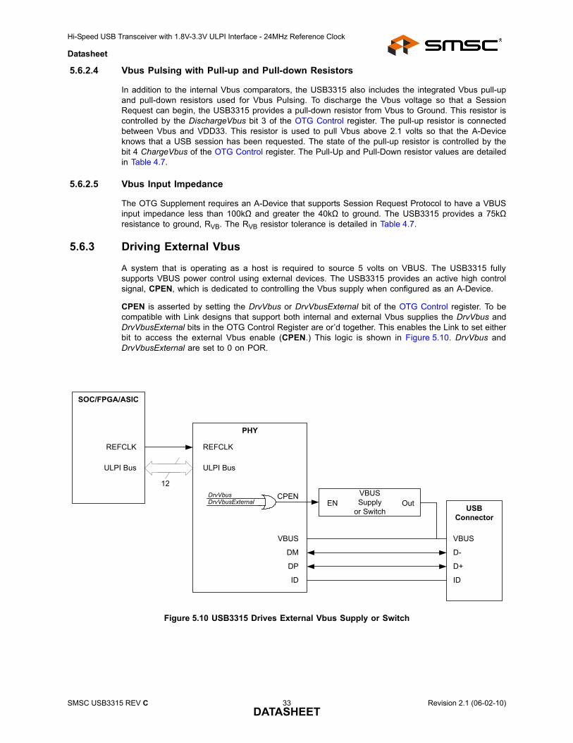
5.6.3 Driving External Vbus
A system that is operating as a host is required to source 5 volts on VBUS. The USB3315 fullysupports VBUS power control using external devices. The USB3315 provides an active high controlsignal, CPEN, which is dedicated to controlling the Vbus supply when configured as an A-Device.
CPEN is asserted by setting the DrvVbus or DrvVbusExternal bit of the OTG Control register. To becompatible with Link designs that support both internal and external Vbus supplies the DrvVbus andDrvVbusExternal bits in the OTG Control Register are or’d together. This enables the Link to set eitherbit to access the external Vbus enable (CPEN.) This logic is shown in Figure 5.10. DrvVbus andDrvVbusExternal are set to 0 on POR.
Figure 5.10 USB3315 Drives External Vbus Supply or Switch
PHY
REFCLK
DM
DP
USBConnector
D-
D+
VBUS
ID ID
VBUS
12
ULPI Bus
SOC/FPGA/ASIC
REFCLK
ULPI Bus
DrvVbusExternalDrvVbus CPEN VBUS
Supplyor Switch
EN Out
SMSC USB3315 REV C 33 Revision 2.1 (06-02-10)DATASHEET
Hi-Speed USB Transceiver with 1.8V-3.3V ULPI Interface - 24MHz Reference Clock
Datasheet
5.7 USB UART SupportThe USB3315 provides support for the USB UART interface as detailed in the ULPI specification andthe CEA-936A specification. The USB3315 can be placed in UART Mode using the method describedin Section 6.4, and the regulator output will automatically switch to the value configured by the UARTRegOutput bits in the USB IO & Power Management register. While in UART mode, the Linestatesignals cannot be monitored on the DATA[0] and DATA[1] pins.
5.8 USB Charger Detection SupportTo support the detection and identification of different types of USB chargers the USB3315 providesintegrated pull-up resistors, RCD, on both DP and DM. These pull-up resistors along with the singleended receivers can be used to help determine the type of USB charger attached. Referenceinformation on implementing charger detection is provided in Section 8.2.
Note: ChargerPullupEnableDP and ChargerPullupEnableDM are enabled in the USB IO & PowerManagement register.
Table 5.6 USB Weak Pull-up Enable
RESETB DP PULLUP ENABLE DM PULLUP ENABLE
0 0 0
1 ChargerPullupEnableDP ChargerPullupEnableDM
Revision 2.1 (06-02-10) 34 SMSC USB3315 REV CDATASHEET
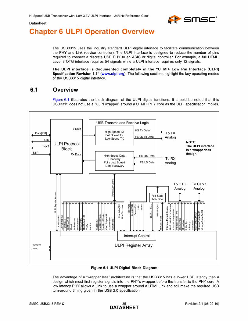
Hi-Speed USB Transceiver with 1.8V-3.3V ULPI Interface - 24MHz Reference Clock
Datasheet
Chapter 6 ULPI Operation Overview
The USB3315 uses the industry standard ULPI digital interface to facilitate communication betweenthe PHY and Link (device controller). The ULPI interface is designed to reduce the number of pinsrequired to connect a discrete USB PHY to an ASIC or digital controller. For example, a full UTMI+Level 3 OTG interface requires 54 signals while a ULPI interface requires only 12 signals.
The ULPI interface is documented completely in the “UTMI+ Low Pin Interface (ULPI)Specification Revision 1.1” (www.ulpi.org). The following sections highlight the key operating modesof the USB3315 digital interface.
6.1 OverviewFigure 6.1 illustrates the block diagram of the ULPI digital functions. It should be noted that thisUSB3315 does not use a “ULPI wrapper” around a UTMI+ PHY core as the ULPI specification implies.
The advantage of a “wrapper less” architecture is that the USB3315 has a lower USB latency than adesign which must first register signals into the PHY’s wrapper before the transfer to the PHY core. Alow latency PHY allows a Link to use a wrapper around a UTMI Link and still make the required USBturn-around timing given in the USB 2.0 specification.
Figure 6.1 ULPI Digital Block Diagram
NOTE:The ULPI interface is a wrapperless design.
PORULPI Register Array
Interrupt Control
6pin
Seria
l Mod
e
Xcvr
Sele
ct[1
:0]
Term
Sel
ect
OpM
ode[
1:0]
Res
et
Susp
endM
3pin
Seria
l Mod
eC
lock
Susp
endM
Auto
Res
ume
Dis
chrg
Vbus
Chr
gVbu
sId
Gnd
Drv
SpkL
eftE
nSp
kRig
htEn
/Mic
En
DpP
ulld
own
Dm
Pulld
own
Swap
DP
/DM
Car
kitM
ode
Reg
Out
put[1
:0]
Cha
rger
Pullu
pEnD
PC
harg
erPu
llupE
nDM
TxdE
nR
xdEn
Indi
cato
r Com
plem
ent
Indi
cato
r Pas
s Th
ru
Use
Exte
rnal
Vbu
s In
dica
tor
IdP
ullU
p
Line
stat
es[1
:0]
Hos
tDis
conn
ect
Inte
rface
Pro
tect
Dis
able
Vbus
Valid
Ses
sion
Valid
Sess
ionE
ndId
Gnd
IdFl
oat
Rid
Con
...St
artR
idVa
lue[
2:0]
Rid
Con
...D
one
Data[7:0] High Speed TXFull Speed TXLow Speed TX
High Speed DataRecovery
Full / Low Speed Data Recovery
ULPI Protocol Block
HS Tx Data
FS/LS Tx Data
HS RX Data
FS/LS Data
DIR
NXT
STP
Tx Data
Rx Data
USB Transmit and Receive Logic
ULP
I Reg
iste
r Acc
ess
RESETB
ULP
I Int
erup
t
Rid State Machine
To RX Analog
To TX Analog
Tran
scei
ver C
ontro
l
To OTG Analog
To Carkit Analog
SMSC USB3315 REV C 35 Revision 2.1 (06-02-10)DATASHEET
Hi-Speed USB Transceiver with 1.8V-3.3V ULPI Interface - 24MHz Reference Clock
Datasheet
RxEndDelay maximum allowed by the UTMI+/ULPI for 8-bit data is 63 high speed clocks. USB3315uses a low latency high speed receiver path to lower the RxEndDelay to 43 high speed clocks. Thislow latency design gives the Link more cycles to make decisions and reduces the Link complexity. Thisis the result of the “wrapper less” architecture of the USB3315. This low RxEndDelay should allowlegacy UTMI Links to use a “wrapper” to convert the UTMI+ interface to a ULPI interface.
In Figure 6.1, a single ULPI Protocol Block decodes the ULPI 8-bit bi-directional bus when the Linkaddresses the PHY. The Link must use the DIR output to determine direction of the ULPI data bus.The USB3315 is the “bus arbitrator”. The ULPI Protocol Block will route data/commands to thetransmitter or the ULPI register array.
6.1.1 ULPI Interface Signals
The UTIM+ Low Pin Interface (ULPI) uses 12-pins to connect a full OTG Host / Device PHY to anSOC. A reduction of external pins on the PHY is accomplished by realizing that many of the relativelystatic configuration pins (xcvrselect[1:0], termselect, opmode[1:0], and DpPullDown DmPulldown to lista few,) can be implemented by having an internal static register array.
An 8-bit bi-directional data bus clocked at 60MHz allows the Link to access this internal register arrayand transfer USB packets to and from the PHY. The remaining 3 pins function to control the data flowand arbitrate the data bus.
Direction of the 8-bit data bus is controlled by the DIR output from the PHY. Another output, NXT, isused to control data flow into and out of the device. Finally, STP, which is in input to the PHY,terminates transfers and is used to start up and resume from Low Power Mode.
The 12 signals are described below in Table 6.1.
USB3315 implements a Single Data Rate (SDR) ULPI interface with all data transfers happening onthe rising edge of the CLKOUT signal supplied by the PHY.
The ULPI interface supports the two basic modes of operation: Synchronous Mode and Low PowerMode. In Synchronous Mode, all signals change synchronously with the 60MHz CLKOUT. In LowPower Mode the clock is off and the lower two bits of the data bus contain the linestate[1:0] signals.Interrupt outputs are generated while in Low Power Mode to enable the Link to receive anasynchronous interrupt when the Linestate, Vbus state, or ID state changes.
Table 6.1 ULPI Interface Signals
SIGNAL DIRECTION DESCRIPTION
CLKOUT OUT 60MHz reference clock output. All ULPI signals are driven synchronous to the rising edge of this clock.
DATA[7:0] I/O 8-bit bi-directional data bus. Bus ownership is determined by DIR. The Link and PHY initiate data transfers by driving a non-zero pattern onto the data bus. ULPI defines interface timing for a single-edge data transfers with respect to rising edge of CLKOUT.
DIR OUT Controls the direction of the data bus. When the PHY has data to transfer to the Link, it drives DIR high to take ownership of the bus. When the PHY has no data to transfer it drives DIR low and monitors the bus for commands from the Link. The PHY will pull DIR high whenever the interface cannot accept data from the Link, such as during PLL start-up.
STP IN The Link asserts STP for one clock cycle to stop the data stream currently on the bus. If the Link is sending data to the PHY, STP indicates the last byte of data was on the bus in the previous cycle.
NXT OUT The PHY asserts NXT to throttle the data. When the Link is sending data to the PHY, NXT indicates when the current byte has been accepted by the PHY. The Link places the next byte on the data bus in the following clock cycle.
Revision 2.1 (06-02-10) 36 SMSC USB3315 REV CDATASHEET
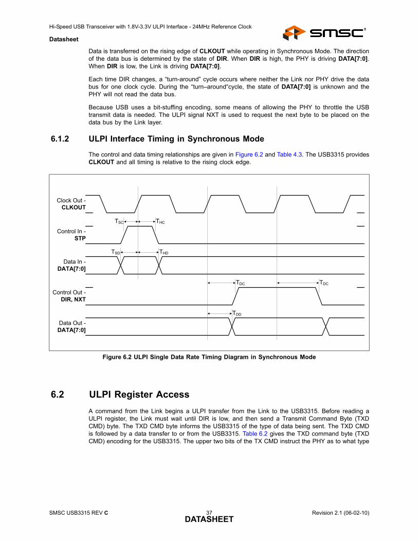
Hi-Speed USB Transceiver with 1.8V-3.3V ULPI Interface - 24MHz Reference Clock
Datasheet
Data is transferred on the rising edge of CLKOUT while operating in Synchronous Mode. The directionof the data bus is determined by the state of DIR. When DIR is high, the PHY is driving DATA[7:0].When DIR is low, the Link is driving DATA[7:0].
Each time DIR changes, a “turn-around” cycle occurs where neither the Link nor PHY drive the databus for one clock cycle. During the “turn–around“cycle, the state of DATA[7:0] is unknown and thePHY will not read the data bus.
Because USB uses a bit-stuffing encoding, some means of allowing the PHY to throttle the USBtransmit data is needed. The ULPI signal NXT is used to request the next byte to be placed on thedata bus by the Link layer.
6.1.2 ULPI Interface Timing in Synchronous Mode
The control and data timing relationships are given in Figure 6.2 and Table 4.3. The USB3315 providesCLKOUT and all timing is relative to the rising clock edge.
6.2 ULPI Register AccessA command from the Link begins a ULPI transfer from the Link to the USB3315. Before reading aULPI register, the Link must wait until DIR is low, and then send a Transmit Command Byte (TXDCMD) byte. The TXD CMD byte informs the USB3315 of the type of data being sent. The TXD CMDis followed by a data transfer to or from the USB3315. Table 6.2 gives the TXD command byte (TXDCMD) encoding for the USB3315. The upper two bits of the TX CMD instruct the PHY as to what type
Figure 6.2 ULPI Single Data Rate Timing Diagram in Synchronous Mode
Clock Out -CLKOUT
Control In - STP
Data In - DATA[7:0]
Control Out - DIR, NXT
Data Out - DATA[7:0]
TSC
TSD
THC
THD
TDC TDC
TDD
SMSC USB3315 REV C 37 Revision 2.1 (06-02-10)DATASHEET
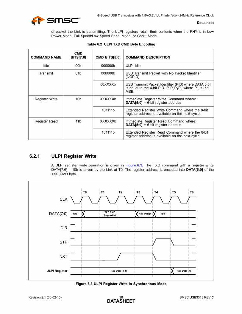
Hi-Speed USB Transceiver with 1.8V-3.3V ULPI Interface - 24MHz Reference Clock
Datasheet
of packet the Link is transmitting. The ULPI registers retain their contents when the PHY is in LowPower Mode, Full Speed/Low Speed Serial Mode, or Carkit Mode.
6.2.1 ULPI Register Write
A ULPI register write operation is given in Figure 6.3. The TXD command with a register writeDATA[7:6] = 10b is driven by the Link at T0. The register address is encoded into DATA[5:0] of theTXD CMD byte.
Table 6.2 ULPI TXD CMD Byte Encoding
COMMAND NAMECMD
BITS[7:6] CMD BITS[5:0] COMMAND DESCRIPTION
Idle 00b 000000b ULPI Idle
Transmit 01b 000000b USB Transmit Packet with No Packet Identifier (NOPID)
00XXXXb USB Transmit Packet Identifier (PID) where DATA[3:0] is equal to the 4-bit PID. P3P2P1P0 where P3 is the MSB.
Register Write 10b XXXXXXb Immediate Register Write Command where: DATA[5:0] = 6-bit register address
101111b Extended Register Write Command where the 8-bit register address is available on the next cycle.
Register Read 11b XXXXXXb Immediate Register Read Command where: DATA[5:0] = 6-bit register address
101111b Extended Register Read Command where the 8-bit register address is available on the next cycle.
Figure 6.3 ULPI Register Write in Synchronous Mode
DIR
CLK
DATA[7:0]
STP
NXT
TXD CMD (reg write) Idle Reg Data[n] Idle
ULPI Register Reg Data [n-1] Reg Data [n]
T0 T1 T2 T3 T5T4 T6
Revision 2.1 (06-02-10) 38 SMSC USB3315 REV CDATASHEET
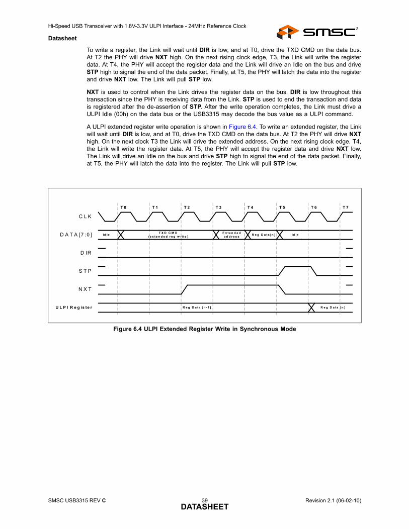
Hi-Speed USB Transceiver with 1.8V-3.3V ULPI Interface - 24MHz Reference Clock
Datasheet
To write a register, the Link will wait until DIR is low, and at T0, drive the TXD CMD on the data bus.At T2 the PHY will drive NXT high. On the next rising clock edge, T3, the Link will write the registerdata. At T4, the PHY will accept the register data and the Link will drive an Idle on the bus and driveSTP high to signal the end of the data packet. Finally, at T5, the PHY will latch the data into the registerand drive NXT low. The Link will pull STP low.
NXT is used to control when the Link drives the register data on the bus. DIR is low throughout thistransaction since the PHY is receiving data from the Link. STP is used to end the transaction and datais registered after the de-assertion of STP. After the write operation completes, the Link must drive aULPI Idle (00h) on the data bus or the USB3315 may decode the bus value as a ULPI command.
A ULPI extended register write operation is shown in Figure 6.4. To write an extended register, the Linkwill wait until DIR is low, and at T0, drive the TXD CMD on the data bus. At T2 the PHY will drive NXThigh. On the next clock T3 the Link will drive the extended address. On the next rising clock edge, T4,the Link will write the register data. At T5, the PHY will accept the register data and drive NXT low.The Link will drive an Idle on the bus and drive STP high to signal the end of the data packet. Finally,at T5, the PHY will latch the data into the register. The Link will pull STP low.
Figure 6.4 ULPI Extended Register Write in Synchronous Mode
D IR
C L K
D A T A [7 :0 ]
S T P
N X T
T X D C M D (e x te n d e d r e g w r it e ) Id le R e g D a t a [ n ] Id le
U L P I R e g is te r R e g D a ta [n - 1 ] R e g D a ta [n ]
T 0 T 1 T 2 T 3 T 5T 4 T 6
E x te n d e da d d r e s s
T 7
SMSC USB3315 REV C 39 Revision 2.1 (06-02-10)DATASHEET
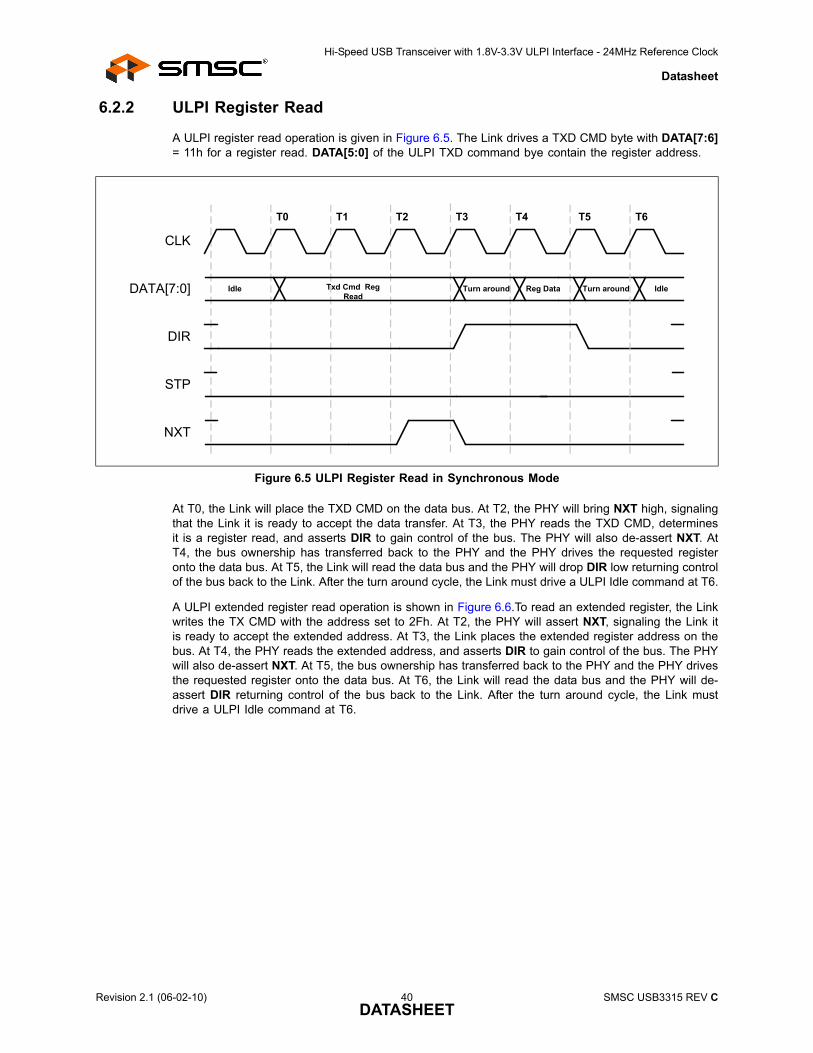
Hi-Speed USB Transceiver with 1.8V-3.3V ULPI Interface - 24MHz Reference Clock
Datasheet
6.2.2 ULPI Register Read
A ULPI register read operation is given in Figure 6.5. The Link drives a TXD CMD byte with DATA[7:6]= 11h for a register read. DATA[5:0] of the ULPI TXD command bye contain the register address.
At T0, the Link will place the TXD CMD on the data bus. At T2, the PHY will bring NXT high, signalingthat the Link it is ready to accept the data transfer. At T3, the PHY reads the TXD CMD, determinesit is a register read, and asserts DIR to gain control of the bus. The PHY will also de-assert NXT. AtT4, the bus ownership has transferred back to the PHY and the PHY drives the requested registeronto the data bus. At T5, the Link will read the data bus and the PHY will drop DIR low returning controlof the bus back to the Link. After the turn around cycle, the Link must drive a ULPI Idle command at T6.
A ULPI extended register read operation is shown in Figure 6.6.To read an extended register, the Linkwrites the TX CMD with the address set to 2Fh. At T2, the PHY will assert NXT, signaling the Link itis ready to accept the extended address. At T3, the Link places the extended register address on thebus. At T4, the PHY reads the extended address, and asserts DIR to gain control of the bus. The PHYwill also de-assert NXT. At T5, the bus ownership has transferred back to the PHY and the PHY drivesthe requested register onto the data bus. At T6, the Link will read the data bus and the PHY will de-assert DIR returning control of the bus back to the Link. After the turn around cycle, the Link mustdrive a ULPI Idle command at T6.
Figure 6.5 ULPI Register Read in Synchronous Mode
DIR
CLK
DATA[7:0]
STP
NXT
Txd Cmd Reg Read Idle
T0
Reg DataTurn around Turn around
T1 T2 T3 T4 T5 T6
Idle
Revision 2.1 (06-02-10) 40 SMSC USB3315 REV CDATASHEET
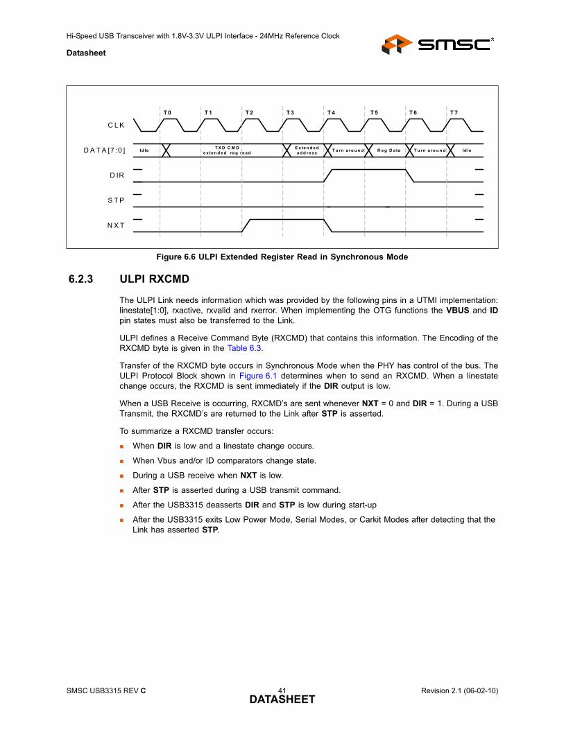
Hi-Speed USB Transceiver with 1.8V-3.3V ULPI Interface - 24MHz Reference Clock
Datasheet
6.2.3 ULPI RXCMD
The ULPI Link needs information which was provided by the following pins in a UTMI implementation:linestate[1:0], rxactive, rxvalid and rxerror. When implementing the OTG functions the VBUS and IDpin states must also be transferred to the Link.
ULPI defines a Receive Command Byte (RXCMD) that contains this information. The Encoding of theRXCMD byte is given in the Table 6.3.
Transfer of the RXCMD byte occurs in Synchronous Mode when the PHY has control of the bus. TheULPI Protocol Block shown in Figure 6.1 determines when to send an RXCMD. When a linestatechange occurs, the RXCMD is sent immediately if the DIR output is low.
When a USB Receive is occurring, RXCMD’s are sent whenever NXT = 0 and DIR = 1. During a USBTransmit, the RXCMD’s are returned to the Link after STP is asserted.
To summarize a RXCMD transfer occurs:
When DIR is low and a linestate change occurs.
When Vbus and/or ID comparators change state.
During a USB receive when NXT is low.
After STP is asserted during a USB transmit command.
After the USB3315 deasserts DIR and STP is low during start-up
After the USB3315 exits Low Power Mode, Serial Modes, or Carkit Modes after detecting that the Link has asserted STP.
Figure 6.6 ULPI Extended Register Read in Synchronous Mode
D IR
C L K
D A T A [7 :0 ]
S T P
N X T
T X D C M De x te n d e d re g re a d Id le
T 0
R e g D a taT u rn a ro u n d T u rn a ro u n d
T 1 T 2 T 3 T 4 T 5 T 6
Id leE x te n d e da d d re s s
T 7
SMSC USB3315 REV C 41 Revision 2.1 (06-02-10)DATASHEET
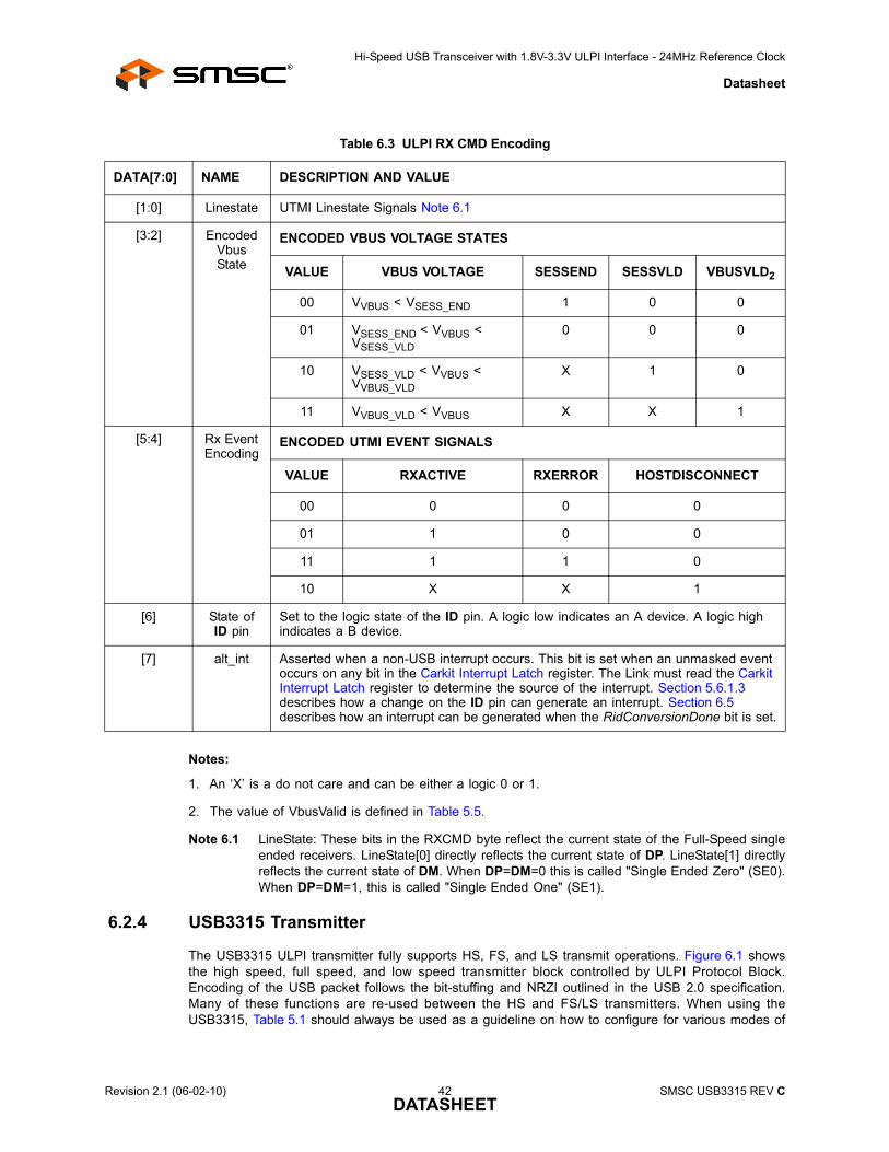
Hi-Speed USB Transceiver with 1.8V-3.3V ULPI Interface - 24MHz Reference Clock
Datasheet
Notes:
1. An ‘X’ is a do not care and can be either a logic 0 or 1.
2. The value of VbusValid is defined in Table 5.5.
Note 6.1 LineState: These bits in the RXCMD byte reflect the current state of the Full-Speed singleended receivers. LineState[0] directly reflects the current state of DP. LineState[1] directlyreflects the current state of DM. When DP=DM=0 this is called "Single Ended Zero" (SE0).When DP=DM=1, this is called "Single Ended One" (SE1).
6.2.4 USB3315 Transmitter
The USB3315 ULPI transmitter fully supports HS, FS, and LS transmit operations. Figure 6.1 showsthe high speed, full speed, and low speed transmitter block controlled by ULPI Protocol Block.Encoding of the USB packet follows the bit-stuffing and NRZI outlined in the USB 2.0 specification.Many of these functions are re-used between the HS and FS/LS transmitters. When using theUSB3315, Table 5.1 should always be used as a guideline on how to configure for various modes of
Table 6.3 ULPI RX CMD Encoding
DATA[7:0] NAME DESCRIPTION AND VALUE
[1:0] Linestate UTMI Linestate Signals Note 6.1
[3:2] Encoded Vbus State
ENCODED VBUS VOLTAGE STATES
VALUE VBUS VOLTAGE SESSEND SESSVLD VBUSVLD2
00 VVBUS < VSESS_END 1 0 0
01 VSESS_END < VVBUS < VSESS_VLD
0 0 0
10 VSESS_VLD < VVBUS < VVBUS_VLD
X 1 0
11 VVBUS_VLD < VVBUS X X 1
[5:4] Rx Event Encoding
ENCODED UTMI EVENT SIGNALS
VALUE RXACTIVE RXERROR HOSTDISCONNECT
00 0 0 0
01 1 0 0
11 1 1 0
10 X X 1
[6] State of ID pin
Set to the logic state of the ID pin. A logic low indicates an A device. A logic high indicates a B device.
[7] alt_int Asserted when a non-USB interrupt occurs. This bit is set when an unmasked event occurs on any bit in the Carkit Interrupt Latch register. The Link must read the Carkit Interrupt Latch register to determine the source of the interrupt. Section 5.6.1.3 describes how a change on the ID pin can generate an interrupt. Section 6.5 describes how an interrupt can be generated when the RidConversionDone bit is set.
Revision 2.1 (06-02-10) 42 SMSC USB3315 REV CDATASHEET
Hi-Speed USB Transceiver with 1.8V-3.3V ULPI Interface - 24MHz Reference Clock
Datasheet
operation. The transmitter decodes the inputs of XcvrSelect[1:0], TermSelect, OpMode[1:0],DpPulldown, and DmPulldown to determine what operation is expected. Users must strictly adhere tothe modes of operation given in Table 5.1.
Several important functions for a device and host are designed into the transmitter blocks.
The USB3315 transmitter will transmit a 32-bit long high speed sync before every high speed packet.In full and low speed modes a 8-bit sync is transmitted.
When the device or host needs to chirp for high speed port negotiation, the OpMode = 10 setting willturn off the bit-stuffing and NRZI encoding in the transmitter. At the end of a chirp, the USB3315OpMode register bits should be changed only after the RXCMD linestate encoding indicates that thetransmitter has completed transmitting. Should the opmode be switched to normal bit-stuffing and NRZIencoding before the transmit pipeline is empty, the remaining data in the pipeline may be transmittedin an bit-stuff encoding format.
Please refer to the ULPI specification for a detailed discussion of USB reset and HS chirp.
6.2.4.1 High Speed Long EOP
When operating as a Hi-Speed host, the USB3315 will automatically generate a 40 bit long End ofPacket (EOP) after a SOF PID (A5h). The USB3315 determines when to send the 40-bit long EOP bydecoding the ULPI TXD CMD bits [3:0] for the SOF. The 40-bit long EOP is only transmitted when theDpPulldown and DmPulldown bits in the OTG Control register are asserted. The Hi-Speed 40-bit longEOP is used to detect a disconnect in high speed mode.
In device mode, the USB3315 will not send a long EOP after a SOF PID.
6.2.4.2 Low Speed Keep-Alive
Low speed keep alive is supported by the USB3315. When in Low speed (10b), the USB3315 will sendout two Low speed bit times of SE0 when a SOF PID is received.
6.2.4.3 UTMI+ Level 3
Pre-amble is supported for UTMI+ Level 3 compatibility. When XcvrSelect is set to (11b) in host mode,(DpPulldown and DmPulldown both asserted) the USB3315 will pre-pend a full speed pre-amble beforethe low speed packet. Full speed rise and fall times are used in this mode. The pre-amble consists ofthe following: Full speed sync, the encoded pre-PID (C3h) and then full speed idle (DP=1 and DM =0). A low speed packet follows with a sync, data and a LS EOP.
The USB3315 will only support UTMI+ Level 3 as a host. The USB3315 does not support UTMI+ Level3 as a peripheral. A UTMI+ Level 3 peripheral is an upstream hub port. The USB3315 will not decodea pre-amble packet intended for a LS device when the USB3315 is configured as the upstream portof a FS hub, XcvrSelect = 11b, DpPulldown = 0b, DmPulldown =0b.
6.2.4.4 Host Resume K
Resume K generation is supported by the USB3315. When the USB3315 exits the suspended (LowPower Mode), the USB3315, when operating as a host, will transmit a K on DP/DM. The transmitterswill end the K with SE0 for two Low Speed bit times. If the USB3315 was operating in high speedmode before the suspend, the host must change to high speed mode before the SE0 ends. SE0 istwo low speed bit times which is about 1.2 us. For more details please see sections 7.1.77 and 7.9 ofthe USB Specification.
In device mode, the resume K will not append an SE0, but release the bus to the correct idle state,depending upon the operational mode as shown in Table 5.1.
The ULPI specification includes a detailed discussion of the resume sequence and the order ofoperations required. To support Host start-up of less than 1mS the USB3315 implements the ULPIAutoResume bit in the Interface Control register. The default AutoResume state is 0 and this bit shouldbe enabled for Host applications.
SMSC USB3315 REV C 43 Revision 2.1 (06-02-10)DATASHEET
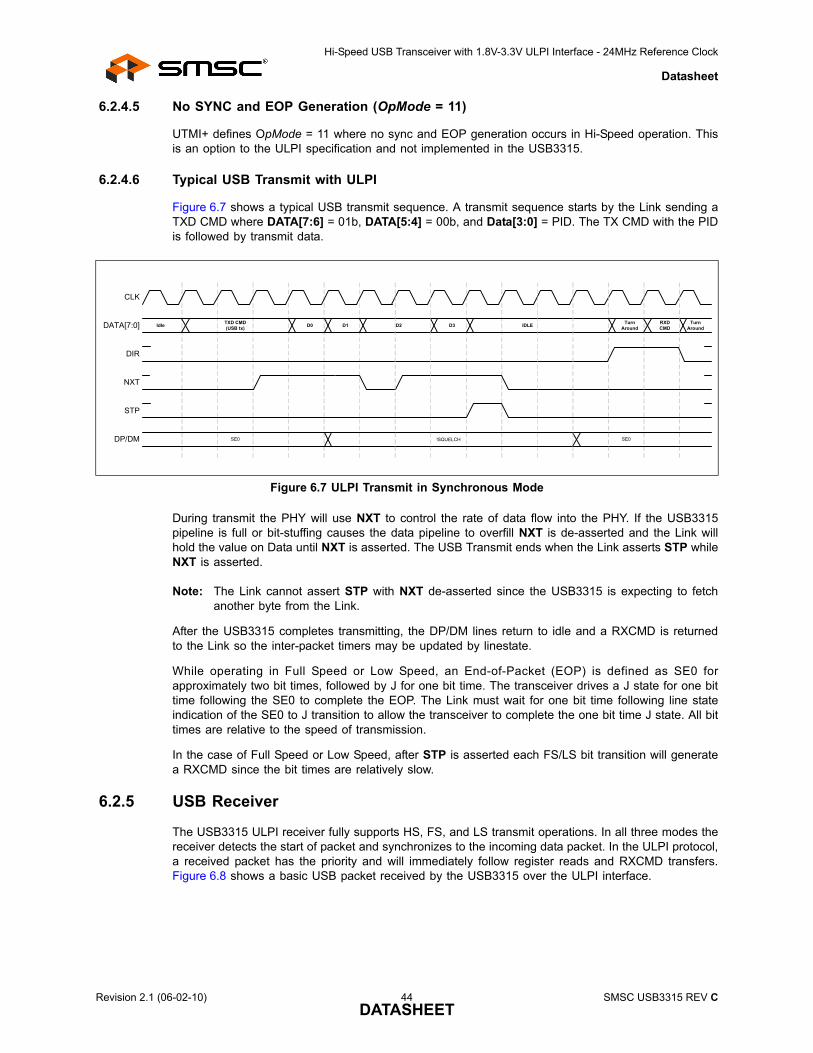
Hi-Speed USB Transceiver with 1.8V-3.3V ULPI Interface - 24MHz Reference Clock
Datasheet
6.2.4.5 No SYNC and EOP Generation (OpMode = 11)
UTMI+ defines OpMode = 11 where no sync and EOP generation occurs in Hi-Speed operation. Thisis an option to the ULPI specification and not implemented in the USB3315.
6.2.4.6 Typical USB Transmit with ULPI
Figure 6.7 shows a typical USB transmit sequence. A transmit sequence starts by the Link sending aTXD CMD where DATA[7:6] = 01b, DATA[5:4] = 00b, and Data[3:0] = PID. The TX CMD with the PIDis followed by transmit data.
During transmit the PHY will use NXT to control the rate of data flow into the PHY. If the USB3315pipeline is full or bit-stuffing causes the data pipeline to overfill NXT is de-asserted and the Link willhold the value on Data until NXT is asserted. The USB Transmit ends when the Link asserts STP whileNXT is asserted.
Note: The Link cannot assert STP with NXT de-asserted since the USB3315 is expecting to fetchanother byte from the Link.
After the USB3315 completes transmitting, the DP/DM lines return to idle and a RXCMD is returnedto the Link so the inter-packet timers may be updated by linestate.
While operating in Full Speed or Low Speed, an End-of-Packet (EOP) is defined as SE0 forapproximately two bit times, followed by J for one bit time. The transceiver drives a J state for one bittime following the SE0 to complete the EOP. The Link must wait for one bit time following line stateindication of the SE0 to J transition to allow the transceiver to complete the one bit time J state. All bittimes are relative to the speed of transmission.
In the case of Full Speed or Low Speed, after STP is asserted each FS/LS bit transition will generatea RXCMD since the bit times are relatively slow.
6.2.5 USB Receiver
The USB3315 ULPI receiver fully supports HS, FS, and LS transmit operations. In all three modes thereceiver detects the start of packet and synchronizes to the incoming data packet. In the ULPI protocol,a received packet has the priority and will immediately follow register reads and RXCMD transfers.Figure 6.8 shows a basic USB packet received by the USB3315 over the ULPI interface.
Figure 6.7 ULPI Transmit in Synchronous Mode
DATA[7:0]
DP/DM
DIR
CLK
STP
NXT
TXD CMD (USB tx) Idle D0 D2 D3 IDLE
SE0 !SQUELCH SE0
Turn Around
Turn Around
RXD CMDD1
Revision 2.1 (06-02-10) 44 SMSC USB3315 REV CDATASHEET
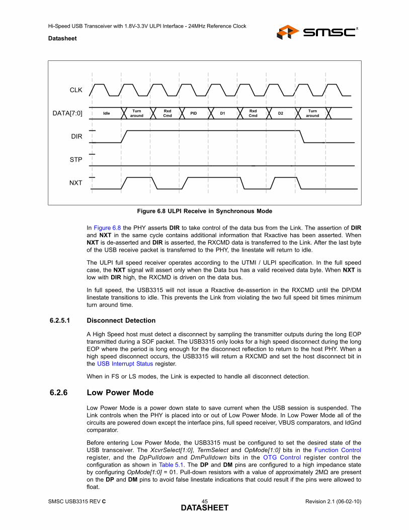
Hi-Speed USB Transceiver with 1.8V-3.3V ULPI Interface - 24MHz Reference Clock
Datasheet
In Figure 6.8 the PHY asserts DIR to take control of the data bus from the Link. The assertion of DIRand NXT in the same cycle contains additional information that Rxactive has been asserted. WhenNXT is de-asserted and DIR is asserted, the RXCMD data is transferred to the Link. After the last byteof the USB receive packet is transferred to the PHY, the linestate will return to idle.
The ULPI full speed receiver operates according to the UTMI / ULPI specification. In the full speedcase, the NXT signal will assert only when the Data bus has a valid received data byte. When NXT islow with DIR high, the RXCMD is driven on the data bus.
In full speed, the USB3315 will not issue a Rxactive de-assertion in the RXCMD until the DP/DMlinestate transitions to idle. This prevents the Link from violating the two full speed bit times minimumturn around time.
6.2.5.1 Disconnect Detection
A High Speed host must detect a disconnect by sampling the transmitter outputs during the long EOPtransmitted during a SOF packet. The USB3315 only looks for a high speed disconnect during the longEOP where the period is long enough for the disconnect reflection to return to the host PHY. When ahigh speed disconnect occurs, the USB3315 will return a RXCMD and set the host disconnect bit inthe USB Interrupt Status register.
When in FS or LS modes, the Link is expected to handle all disconnect detection.
6.2.6 Low Power Mode
Low Power Mode is a power down state to save current when the USB session is suspended. TheLink controls when the PHY is placed into or out of Low Power Mode. In Low Power Mode all of thecircuits are powered down except the interface pins, full speed receiver, VBUS comparators, and IdGndcomparator.
Before entering Low Power Mode, the USB3315 must be configured to set the desired state of theUSB transceiver. The XcvrSelect[1:0], TermSelect and OpMode[1:0] bits in the Function Controlregister, and the DpPulldown and DmPulldown bits in the OTG Control register control theconfiguration as shown in Table 5.1. The DP and DM pins are configured to a high impedance stateby configuring OpMode[1:0] = 01. Pull-down resistors with a value of approximately 2MΩ are presenton the DP and DM pins to avoid false linestate indications that could result if the pins were allowed tofloat.
Figure 6.8 ULPI Receive in Synchronous Mode
DIR
CLK
DATA[7:0]
STP
NXT
Rxd Cmd Idle Turn
around PID D1 Rxd Cmd D2 Turn
around
SMSC USB3315 REV C 45 Revision 2.1 (06-02-10)DATASHEET
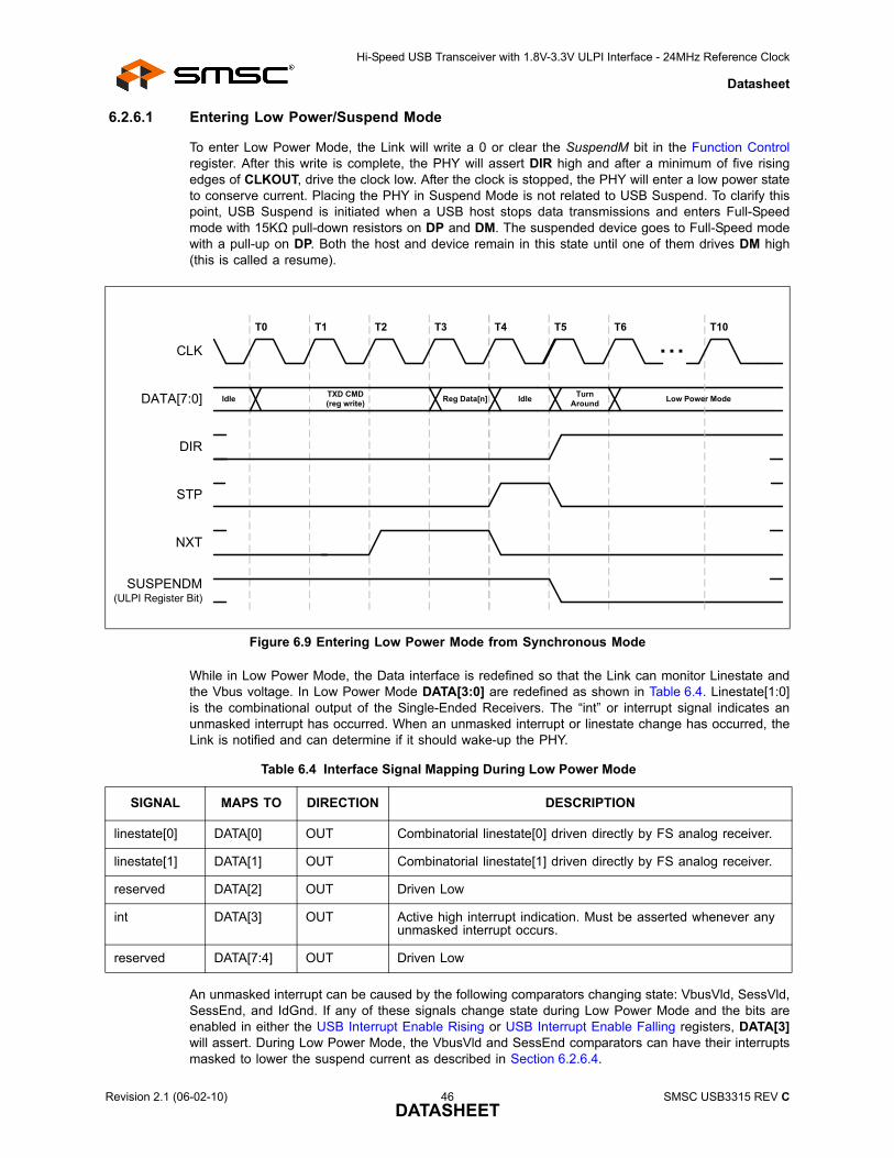
Hi-Speed USB Transceiver with 1.8V-3.3V ULPI Interface - 24MHz Reference Clock
Datasheet
6.2.6.1 Entering Low Power/Suspend Mode
To enter Low Power Mode, the Link will write a 0 or clear the SuspendM bit in the Function Controlregister. After this write is complete, the PHY will assert DIR high and after a minimum of five risingedges of CLKOUT, drive the clock low. After the clock is stopped, the PHY will enter a low power stateto conserve current. Placing the PHY in Suspend Mode is not related to USB Suspend. To clarify thispoint, USB Suspend is initiated when a USB host stops data transmissions and enters Full-Speedmode with 15KΩ pull-down resistors on DP and DM. The suspended device goes to Full-Speed modewith a pull-up on DP. Both the host and device remain in this state until one of them drives DM high(this is called a resume).
While in Low Power Mode, the Data interface is redefined so that the Link can monitor Linestate andthe Vbus voltage. In Low Power Mode DATA[3:0] are redefined as shown in Table 6.4. Linestate[1:0]is the combinational output of the Single-Ended Receivers. The “int” or interrupt signal indicates anunmasked interrupt has occurred. When an unmasked interrupt or linestate change has occurred, theLink is notified and can determine if it should wake-up the PHY.
An unmasked interrupt can be caused by the following comparators changing state: VbusVld, SessVld,SessEnd, and IdGnd. If any of these signals change state during Low Power Mode and the bits areenabled in either the USB Interrupt Enable Rising or USB Interrupt Enable Falling registers, DATA[3]will assert. During Low Power Mode, the VbusVld and SessEnd comparators can have their interruptsmasked to lower the suspend current as described in Section 6.2.6.4.
Figure 6.9 Entering Low Power Mode from Synchronous Mode
Table 6.4 Interface Signal Mapping During Low Power Mode
SIGNAL MAPS TO DIRECTION DESCRIPTION
linestate[0] DATA[0] OUT Combinatorial linestate[0] driven directly by FS analog receiver.
linestate[1] DATA[1] OUT Combinatorial linestate[1] driven directly by FS analog receiver.
reserved DATA[2] OUT Driven Low
int DATA[3] OUT Active high interrupt indication. Must be asserted whenever any unmasked interrupt occurs.
reserved DATA[7:4] OUT Driven Low
DIR
CLK
DATA[7:0]
STP
NXT
TXD CMD (reg write) Idle Reg Data[n] Idle
T0 T1 T2 T3 T5T4 T6 T10
TurnAround Low Power Mode
SUSPENDM(ULPI Register Bit)
...
Revision 2.1 (06-02-10) 46 SMSC USB3315 REV CDATASHEET
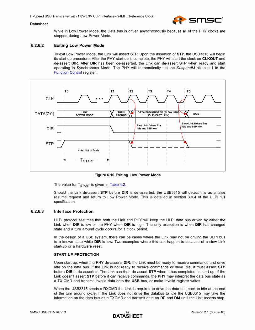
Hi-Speed USB Transceiver with 1.8V-3.3V ULPI Interface - 24MHz Reference Clock
Datasheet
While in Low Power Mode, the Data bus is driven asynchronously because all of the PHY clocks arestopped during Low Power Mode.
6.2.6.2 Exiting Low Power Mode
To exit Low Power Mode, the Link will assert STP. Upon the assertion of STP, the USB3315 will beginits start-up procedure. After the PHY start-up is complete, the PHY will start the clock on CLKOUT andde-assert DIR. After DIR has been de-asserted, the Link can de-assert STP when ready and startoperating in Synchronous Mode. The PHY will automatically set the SuspendM bit to a 1 in theFunction Control register.
The value for TSTART is given in Table 4.2.
Should the Link de-assert STP before DIR is de-asserted, the USB3315 will detect this as a falseresume request and return to Low Power Mode. This is detailed in section 3.9.4 of the ULPI 1.1specification.
6.2.6.3 Interface Protection
ULPI protocol assumes that both the Link and PHY will keep the ULPI data bus driven by either theLink when DIR is low or the PHY when DIR is high. The only exception is when DIR has changedstate and a turn around cycle occurs for 1 clock period.
In the design of a USB system, there can be cases where the Link may not be driving the ULPI busto a known state while DIR is low. Two examples where this can happen is because of a slow Linkstart-up or a hardware reset.
START UP PROTECTION
Upon start-up, when the PHY de-asserts DIR, the Link must be ready to receive commands and driveIdle on the data bus. If the Link is not ready to receive commands or drive Idle, it must assert STPbefore DIR is de-asserted. The Link can then de-assert STP when it has completed its start-up. If theLink doesn’t assert STP before it can receive commands, the PHY may interpret the data bus state asa TX CMD and transmit invalid data onto the USB bus, or make invalid register writes.
When the USB3315 sends a RXCMD the Link is required to drive the data bus back to idle at the endof the turn around cycle. If the Link does not drive the databus to idle the USB3315 may take theinformation on the data bus as a TXCMD and transmit data on DP and DM until the Link asserts stop.
Figure 6.10 Exiting Low Power Mode
DIR
CLK
DATA[7:0]
STP
TURNAROUND LOW
POWER MODEDATA BUS IGNORED (SLOW LINK)
IDLE (FAST LINK) IDLE
T0 T1 T2 T3 T5T4
Slow Link Drives Bus Idle and STP lowFast Link Drives Bus
Idle and STP low
...
Note: Not to Scale
TSTART
SMSC USB3315 REV C 47 Revision 2.1 (06-02-10)DATASHEET
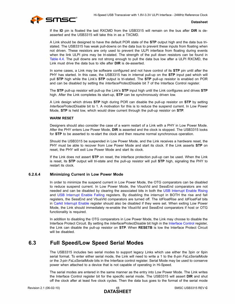
Hi-Speed USB Transceiver with 1.8V-3.3V ULPI Interface - 24MHz Reference Clock
Datasheet
If the ID pin is floated the last RXCMD from the USB3315 will remain on the bus after DIR is de-asserted and the USB3315 will take this in as a TXCMD.
A Link should be designed to have the default POR state of the STP output high and the data bus tri-stated. The USB3315 has weak pull-downs on the data bus to prevent these inputs from floating whennot driven. These resistors are only used to prevent the ULPI interface from floating during eventswhen the link ULPI pins may be tri-stated. The strength of the pull down resistors can be found inTable 4.4. The pull downs are not strong enough to pull the data bus low after a ULPI RXCMD, theLink must drive the data bus to idle after DIR is de-asserted.
In some cases, a Link may be software configured and not have control of its STP pin until after thePHY has started. In this case, the USB3315 has in internal pull-up on the STP input pad which willpull STP high while the Link’s STP output is tri-stated. The STP pull-up resistor is enabled on PORand can be disabled by setting the InterfaceProtectDisable bit 7 of the Interface Control register.
The STP pull-up resistor will pull-up the Link’s STP input high until the Link configures and drives STPhigh. After the Link completes its start-up, STP can be synchronously driven low.
A Link design which drives STP high during POR can disable the pull-up resistor on STP by settingInterfaceProtectDisable bit to 1. A motivation for this is to reduce the suspend current. In Low PowerMode, STP is held low, which would draw current through the pull-up resistor on STP.
WARM RESET
Designers should also consider the case of a warm restart of a Link with a PHY in Low Power Mode.After the PHY enters Low Power Mode, DIR is asserted and the clock is stopped. The USB3315 looksfor STP to be asserted to re-start the clock and then resume normal synchronous operation.
Should the USB3315 be suspended in Low Power Mode, and the Link receives a hardware reset, thePHY must be able to recover from Low Power Mode and start its clock. If the Link asserts STP onreset, the PHY will exit Low Power Mode and start its clock.
If the Link does not assert STP on reset, the interface protection pull-up can be used. When the Linkis reset, its STP output will tri-state and the pull-up resistor will pull STP high, signaling the PHY torestart its clock.
6.2.6.4 Minimizing Current in Low Power Mode
In order to minimize the suspend current in Low Power Mode, the OTG comparators can be disabledto reduce suspend current. In Low Power Mode, the VbusVld and SessEnd comparators are notneeded and can be disabled by clearing the associated bits in both the USB Interrupt Enable Risingand USB Interrupt Enable Falling registers. By disabling the interrupt in BOTH the rise and fallregisters, the SessEnd and VbusVld comparators are turned off. The IdFloatRise and IdFloatFall bitsin Carkit Interrupt Enable register should also be disabled if they were set. When exiting Low PowerMode, the Link should immediately re-enable the VbusVld and SessEnd comparators if host or OTGfunctionality is required.
In addition to disabling the OTG comparators in Low Power Mode, the Link may choose to disable theInterface Protect Circuit. By setting the InterfaceProtectDisable bit high in the Interface Control register,the Link can disable the pull-up resistor on STP. When RESETB is low the Interface Protect Circuitwill be disabled.
6.3 Full Speed/Low Speed Serial ModesThe USB3315 includes two serial modes to support legacy Links which use either the 3pin or 6pinserial format. To enter either serial mode, the Link will need to write a 1 to the 6-pin FsLsSerialModeor the 3-pin FsLsSerialMode bits in the Interface control register. Serial Mode may be used to conservepower when attached to a device that is not capable of operating in Hi-Speed.
The serial modes are entered in the same manner as the entry into Low Power Mode. The Link writesthe Interface Control register bit for the specific serial mode. The USB3315 will assert DIR and shutoff the clock after at least five clock cycles. Then the data bus goes to the format of the serial mode
Revision 2.1 (06-02-10) 48 SMSC USB3315 REV CDATASHEET
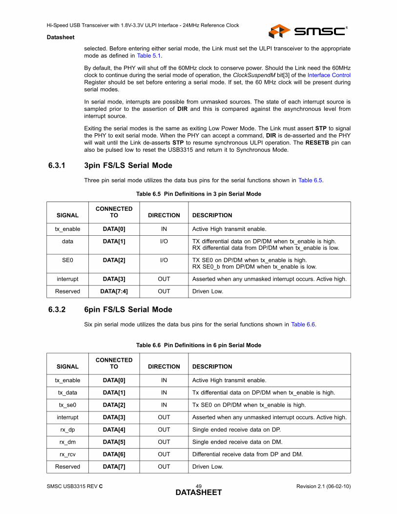
Hi-Speed USB Transceiver with 1.8V-3.3V ULPI Interface - 24MHz Reference Clock
Datasheet
selected. Before entering either serial mode, the Link must set the ULPI transceiver to the appropriatemode as defined in Table 5.1.
By default, the PHY will shut off the 60MHz clock to conserve power. Should the Link need the 60MHzclock to continue during the serial mode of operation, the ClockSuspendM bit[3] of the Interface ControlRegister should be set before entering a serial mode. If set, the 60 MHz clock will be present duringserial modes.
In serial mode, interrupts are possible from unmasked sources. The state of each interrupt source issampled prior to the assertion of DIR and this is compared against the asynchronous level frominterrupt source.
Exiting the serial modes is the same as exiting Low Power Mode. The Link must assert STP to signalthe PHY to exit serial mode. When the PHY can accept a command, DIR is de-asserted and the PHYwill wait until the Link de-asserts STP to resume synchronous ULPI operation. The RESETB pin canalso be pulsed low to reset the USB3315 and return it to Synchronous Mode.
6.3.1 3pin FS/LS Serial Mode
Three pin serial mode utilizes the data bus pins for the serial functions shown in Table 6.5.
6.3.2 6pin FS/LS Serial Mode
Six pin serial mode utilizes the data bus pins for the serial functions shown in Table 6.6.
Table 6.5 Pin Definitions in 3 pin Serial Mode
SIGNALCONNECTED
TO DIRECTION DESCRIPTION
tx_enable DATA[0] IN Active High transmit enable.
data DATA[1] I/O TX differential data on DP/DM when tx_enable is high.RX differential data from DP/DM when tx_enable is low.
SE0 DATA[2] I/O TX SE0 on DP/DM when tx_enable is high.RX SE0_b from DP/DM when tx_enable is low.
interrupt DATA[3] OUT Asserted when any unmasked interrupt occurs. Active high.
Reserved DATA[7:4] OUT Driven Low.
Table 6.6 Pin Definitions in 6 pin Serial Mode
SIGNALCONNECTED
TO DIRECTION DESCRIPTION
tx_enable DATA[0] IN Active High transmit enable.
tx_data DATA[1] IN Tx differential data on DP/DM when tx_enable is high.
tx_se0 DATA[2] IN Tx SE0 on DP/DM when tx_enable is high.
interrupt DATA[3] OUT Asserted when any unmasked interrupt occurs. Active high.
rx_dp DATA[4] OUT Single ended receive data on DP.
rx_dm DATA[5] OUT Single ended receive data on DM.
rx_rcv DATA[6] OUT Differential receive data from DP and DM.
Reserved DATA[7] OUT Driven Low.
SMSC USB3315 REV C 49 Revision 2.1 (06-02-10)DATASHEET
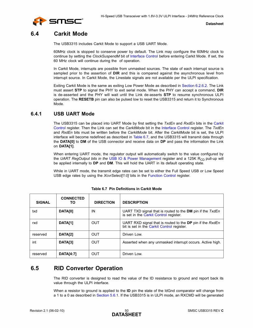
Hi-Speed USB Transceiver with 1.8V-3.3V ULPI Interface - 24MHz Reference Clock
Datasheet
6.4 Carkit ModeThe USB3315 includes Carkit Mode to support a USB UART Mode.
60MHz clock is stopped to conserve power by default. The Link may configure the 60MHz clock tocontinue by setting the ClockSuspendM bit of Interface Control before entering Carkit Mode. If set, the60 MHz clock will continue during the of operation.
In Carkit Mode, interrupts are possible from unmasked sources. The state of each interrupt source issampled prior to the assertion of DIR and this is compared against the asynchronous level frominterrupt source. In Carkit Mode, the Linestate signals are not available per the ULPI specification.
Exiting Carkit Mode is the same as exiting Low Power Mode as described in Section 6.2.6.2. The Linkmust assert STP to signal the PHY to exit serial mode. When the PHY can accept a command, DIRis de-asserted and the PHY will wait until the Link de-asserts STP to resume synchronous ULPIoperation. The RESETB pin can also be pulsed low to reset the USB3315 and return it to SynchronousMode.
6.4.1 USB UART Mode
The USB3315 can be placed into UART Mode by first setting the TxdEn and RxdEn bits in the CarkitControl register. Then the Link can set the CarkitMode bit in the Interface Control register. The TxdEnand RxdEn bits must be written before the CarkitMode bit. After the CarkitMode bit is set, the ULPIinterface will become redefined as described in Table 6.7, and the USB3315 will transmit data throughthe DATA[0] to DM of the USB connector and receive data on DP and pass the information the Linkon DATA[1].
When entering UART mode, the regulator output will automatically switch to the value configured bythe UART RegOutput bits in the USB IO & Power Management register and a 125K RCD pull-up willbe applied internally to DP and DM. This will hold the UART in its default operating state.
While in UART mode, the transmit edge rates can be set to either the Full Speed USB or Low SpeedUSB edge rates by using the XcvrSelect[1:0] bits in the Function Control register.
6.5 RID Converter OperationThe RID converter is designed to read the value of the ID resistance to ground and report back itsvalue through the ULPI interface.
When a resistor to ground is applied to the ID pin the state of the IdGnd comparator will change froma 1 to a 0 as described in Section 5.6.1. If the USB3315 is in ULPI mode, an RXCMD will be generated
Table 6.7 Pin Definitions in Carkit Mode
SIGNALCONNECTED
TO DIRECTION DESCRIPTION
txd DATA[0] IN UART TXD signal that is routed to the DM pin if the TxdEn is set in the Carkit Control register.
rxd DATA[1] OUT UART RXD signal that is routed to the DP pin if the RxdEn bit is set in the Carkit Control register.
reserved DATA[2] OUT Driven Low.
int DATA[3] OUT Asserted when any unmasked interrupt occurs. Active high.
reserved DATA[4:7] OUT Driven Low.
Revision 2.1 (06-02-10) 50 SMSC USB3315 REV CDATASHEET
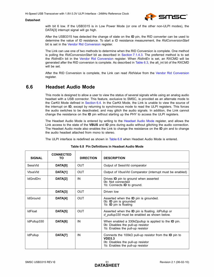
Hi-Speed USB Transceiver with 1.8V-3.3V ULPI Interface - 24MHz Reference Clock
Datasheet
with bit 6 low. If the USB3315 is in Low Power Mode (or one of the other non-ULPI modes), theDATA[3] interrupt signal will go high.
After the USB3315 has detected the change of state on the ID pin, the RID converter can be used todetermine the value of ID resistance. To start a ID resistance measurement, the RidConversionStartbit is set in the Vendor Rid Conversion register.
The Link can use one of two methods to determine when the RID Conversion is complete. One methodis polling the RidConversionStart bit as described in Section 7.1.4.3. The preferred method is to setthe RidIntEn bit in the Vendor Rid Conversion register. When RidIntEn is set, an RXCMD will begenerated after the RID conversion is complete. As described in Table 6.3, the alt_int bit of the RXCMDwill be set.
After the RID Conversion is complete, the Link can read RidValue from the Vendor Rid Conversionregister.
6.6 Headset Audio ModeThis mode is designed to allow a user to view the status of several signals while using an analog audioheadset with a USB connector. This feature, exclusive to SMSC, is provided as an alternate mode tothe CarKit Mode defined in Section 6.4. In the CarKit Mode, the Link is unable to view the source ofthe interrupt on ID, except by returning to synchronous mode to read the ULPI registers. This forcesthe audio switches to be deactivated, and may glitch the audio signals. In addition, the Link cannotchange the resistance on the ID pin without starting up the PHY to access the ULPI registers.
The Headset Audio Mode is entered by writing to the Headset Audio Mode register, and allows theLink access to the state of the VBUS and ID pins during audio without glitching the audio connection.The Headset Audio mode also enables the Link to change the resistance on the ID pin and to changethe audio headset attached from mono to stereo.
The ULPI interface is redefined as shown in Table 6.8 when Headset Audio Mode is entered.
Table 6.8 Pin Definitions in Headset Audio Mode
SIGNALCONNECTED
TO DIRECTION DESCRIPTION
SessVld DATA[0] OUT Output of SessVld comparator
VbusVld DATA[1] OUT Output of VbusVld Comparator (interrupt must be enabled)
IdGndDrv DATA[2] IN Drives ID pin to ground when asserted0b: Not connected1b: Connects ID to ground.
DATA[3] OUT Driven low
IdGround DATA[4] OUT Asserted when the ID pin is grounded.0b: ID pin is grounded1b: ID pin is floating
IdFloat DATA[5] OUT Asserted when the ID pin is floating. IdPullup or d_pullup330 must be enabled as shown below.
IdPullup330 DATA[6] IN When enabled a 330kΩpullup is applied to the ID pin. 0b: Disables the pull-up resistor1b: Enables the pull-up resistor
IdPullup DATA[7] IN Connects the 100kΩ pull-up resistor from the ID pin to VDD3.30b: Disables the pull-up resistor1b: Enables the pull-up resistor
SMSC USB3315 REV C 51 Revision 2.1 (06-02-10)DATASHEET
Hi-Speed USB Transceiver with 1.8V-3.3V ULPI Interface - 24MHz Reference Clock
Datasheet
Exiting Headset Audio Mode is the same as exiting Low Power Mode as described in Section 6.2.6.2.The Link must assert STP to signal the PHY to exit. When the PHY can accept a command, DIR isde-asserted and the PHY will wait until the Link de-asserts STP to resume synchronous ULPIoperation. The RESETB pin can also be pulsed low to reset the USB3315 and return it to SynchronousMode.
Revision 2.1 (06-02-10) 52 SMSC USB3315 REV CDATASHEET
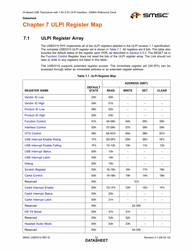
Hi-Speed USB Transceiver with 1.8V-3.3V ULPI Interface - 24MHz Reference Clock
Datasheet
Chapter 7 ULPI Register Map
7.1 ULPI Register ArrayThe USB3315 PHY implements all of the ULPI registers detailed in the ULPI revision 1.1 specification.The complete USB3315 ULPI register set is shown in Table 7.1. All registers are 8 bits. This table alsoincludes the default states of the register upon POR, as described in Section 5.5.2. The RESET bit inthe Function Control Register does not reset the bits of the ULPI register array. The Link should notread or write to any registers not listed in this table.
The USB3315 supports extended register access. The immediate register set (00-3Fh) can beaccessed through either an immediate address or an extended register address..
Table 7.1 ULPI Register Map
REGISTER NAMEDEFAULT
STATE
ADDRESS (6BIT)
READ WRITE SET CLEAR
Vendor ID Low 24h 00h - - -
Vendor ID High 04h 01h - - -
Product ID Low 06h 02h - - -
Product ID High 00h 03h - - -
Function Control 41h 04-06h 04h 05h 06h
Interface Control 00h 07-09h 07h 08h 09h
OTG Control 06h 0A-0Ch 0Ah 0Bh 0Ch
USB Interrupt Enable Rising 1Fh 0D-0Fh 0Dh 0Eh 0Fh
USB Interrupt Enable Falling 1Fh 10-12h 10h 11h 12h
USB Interrupt Status 00h 13h - - -
USB Interrupt Latch 00h 14h - - -
Debug 00h 15h - - -
Scratch Register 00h 16-18h 16h 17h 18h
Carkit Control 00h 19-1Bh 19h 1Ah 1Bh
Reserved 00h 1Ch
Carkit Interrupt Enable 00h 1D-1Fh 1Dh 1Eh 1Fh
Carkit Interrupt Status 00h 20h - - -
Carkit Interrupt Latch 00h 21h - - -
Reserved 00h 22-30h
HS TX Boost 00h 31h 31h - -
Reserved 00h 32h 32h - -
Headset Audio Mode 00h 33h 33h - -
Reserved 00h 34-35h
SMSC USB3315 REV C 53 Revision 2.1 (06-02-10)DATASHEET
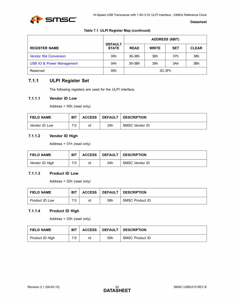
Hi-Speed USB Transceiver with 1.8V-3.3V ULPI Interface - 24MHz Reference Clock
Datasheet
7.1.1 ULPI Register Set
The following registers are used for the ULPI interface.
7.1.1.1 Vendor ID Low
Address = 00h (read only)
7.1.1.2 Vendor ID High
Address = 01h (read only)
7.1.1.3 Product ID Low
Address = 02h (read only)
7.1.1.4 Product ID High
Address = 03h (read only)
Vendor Rid Conversion 00h 36-38h 36h 37h 38h
USB IO & Power Management 04h 39-3Bh 39h 3Ah 3Bh
Reserved 00h 3C-3Fh
FIELD NAME BIT ACCESS DEFAULT DESCRIPTION
Vendor ID Low 7:0 rd 24h SMSC Vendor ID
FIELD NAME BIT ACCESS DEFAULT DESCRIPTION
Vendor ID High 7:0 rd 04h SMSC Vendor ID
FIELD NAME BIT ACCESS DEFAULT DESCRIPTION
Product ID Low 7:0 rd 06h SMSC Product ID
FIELD NAME BIT ACCESS DEFAULT DESCRIPTION
Product ID High 7:0 rd 00h SMSC Product ID
Table 7.1 ULPI Register Map (continued)
REGISTER NAMEDEFAULT
STATE
ADDRESS (6BIT)
READ WRITE SET CLEAR
Revision 2.1 (06-02-10) 54 SMSC USB3315 REV CDATASHEET
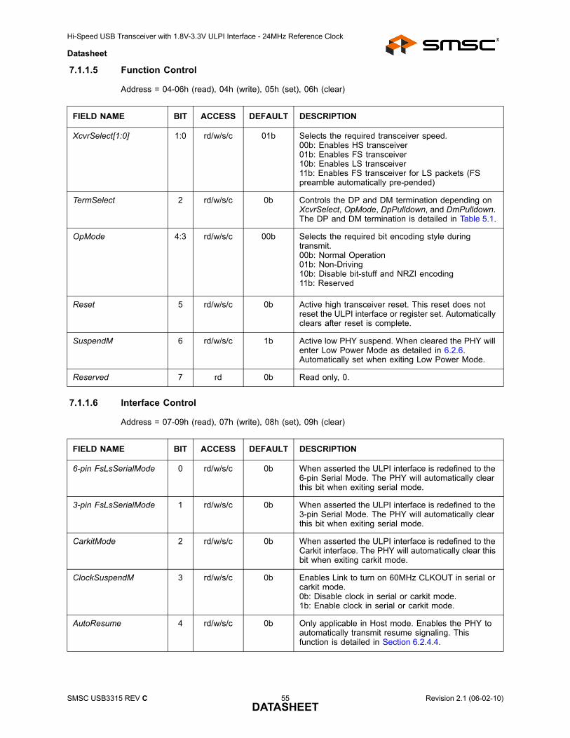
Hi-Speed USB Transceiver with 1.8V-3.3V ULPI Interface - 24MHz Reference Clock
Datasheet
7.1.1.5 Function Control
Address = 04-06h (read), 04h (write), 05h (set), 06h (clear)
7.1.1.6 Interface Control
Address = 07-09h (read), 07h (write), 08h (set), 09h (clear)
FIELD NAME BIT ACCESS DEFAULT DESCRIPTION
XcvrSelect[1:0] 1:0 rd/w/s/c 01b Selects the required transceiver speed.00b: Enables HS transceiver01b: Enables FS transceiver10b: Enables LS transceiver11b: Enables FS transceiver for LS packets (FS preamble automatically pre-pended)
TermSelect 2 rd/w/s/c 0b Controls the DP and DM termination depending on XcvrSelect, OpMode, DpPulldown, and DmPulldown. The DP and DM termination is detailed in Table 5.1.
OpMode 4:3 rd/w/s/c 00b Selects the required bit encoding style during transmit.00b: Normal Operation01b: Non-Driving10b: Disable bit-stuff and NRZI encoding11b: Reserved
Reset 5 rd/w/s/c 0b Active high transceiver reset. This reset does not reset the ULPI interface or register set. Automatically clears after reset is complete.
SuspendM 6 rd/w/s/c 1b Active low PHY suspend. When cleared the PHY will enter Low Power Mode as detailed in 6.2.6. Automatically set when exiting Low Power Mode.
Reserved 7 rd 0b Read only, 0.
FIELD NAME BIT ACCESS DEFAULT DESCRIPTION
6-pin FsLsSerialMode 0 rd/w/s/c 0b When asserted the ULPI interface is redefined to the 6-pin Serial Mode. The PHY will automatically clear this bit when exiting serial mode.
3-pin FsLsSerialMode 1 rd/w/s/c 0b When asserted the ULPI interface is redefined to the 3-pin Serial Mode. The PHY will automatically clear this bit when exiting serial mode.
CarkitMode 2 rd/w/s/c 0b When asserted the ULPI interface is redefined to the Carkit interface. The PHY will automatically clear this bit when exiting carkit mode.
ClockSuspendM 3 rd/w/s/c 0b Enables Link to turn on 60MHz CLKOUT in serial or carkit mode.0b: Disable clock in serial or carkit mode.1b: Enable clock in serial or carkit mode.
AutoResume 4 rd/w/s/c 0b Only applicable in Host mode. Enables the PHY to automatically transmit resume signaling. This function is detailed in Section 6.2.4.4.
SMSC USB3315 REV C 55 Revision 2.1 (06-02-10)DATASHEET
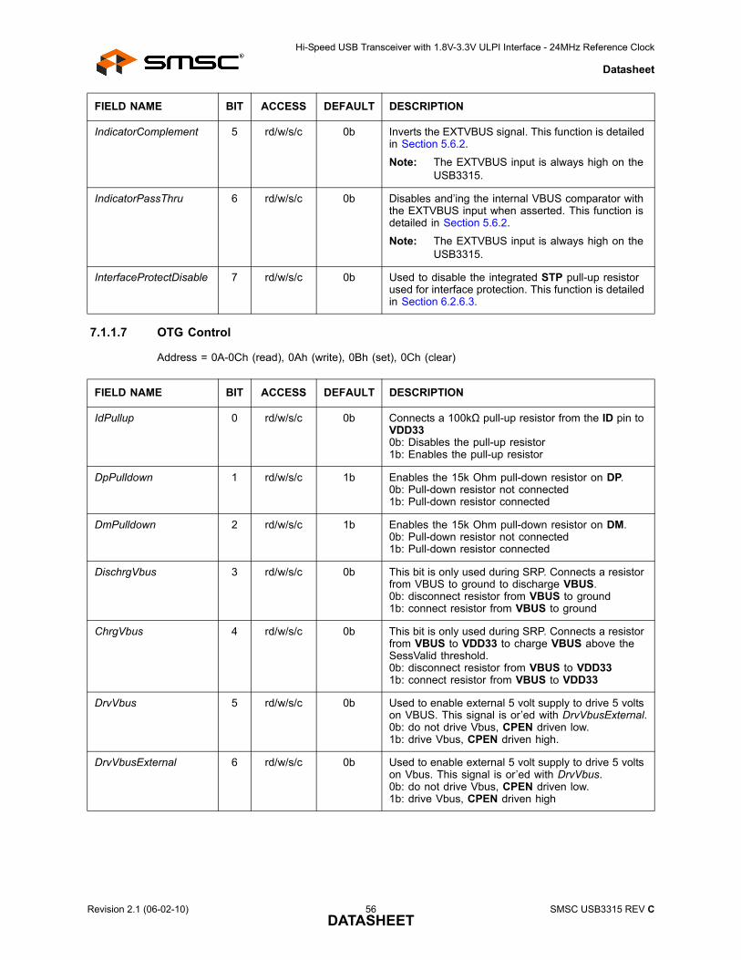
Hi-Speed USB Transceiver with 1.8V-3.3V ULPI Interface - 24MHz Reference Clock
Datasheet
7.1.1.7 OTG Control
Address = 0A-0Ch (read), 0Ah (write), 0Bh (set), 0Ch (clear)
IndicatorComplement 5 rd/w/s/c 0b Inverts the EXTVBUS signal. This function is detailed in Section 5.6.2.
Note: The EXTVBUS input is always high on the USB3315.
IndicatorPassThru 6 rd/w/s/c 0b Disables and’ing the internal VBUS comparator with the EXTVBUS input when asserted. This function is detailed in Section 5.6.2.
Note: The EXTVBUS input is always high on the USB3315.
InterfaceProtectDisable 7 rd/w/s/c 0b Used to disable the integrated STP pull-up resistor used for interface protection. This function is detailed in Section 6.2.6.3.
FIELD NAME BIT ACCESS DEFAULT DESCRIPTION
IdPullup 0 rd/w/s/c 0b Connects a 100kΩ pull-up resistor from the ID pin to VDD330b: Disables the pull-up resistor1b: Enables the pull-up resistor
DpPulldown 1 rd/w/s/c 1b Enables the 15k Ohm pull-down resistor on DP.0b: Pull-down resistor not connected1b: Pull-down resistor connected
DmPulldown 2 rd/w/s/c 1b Enables the 15k Ohm pull-down resistor on DM.0b: Pull-down resistor not connected1b: Pull-down resistor connected
DischrgVbus 3 rd/w/s/c 0b This bit is only used during SRP. Connects a resistor from VBUS to ground to discharge VBUS. 0b: disconnect resistor from VBUS to ground1b: connect resistor from VBUS to ground
ChrgVbus 4 rd/w/s/c 0b This bit is only used during SRP. Connects a resistor from VBUS to VDD33 to charge VBUS above the SessValid threshold.0b: disconnect resistor from VBUS to VDD331b: connect resistor from VBUS to VDD33
DrvVbus 5 rd/w/s/c 0b Used to enable external 5 volt supply to drive 5 volts on VBUS. This signal is or’ed with DrvVbusExternal.0b: do not drive Vbus, CPEN driven low.1b: drive Vbus, CPEN driven high.
DrvVbusExternal 6 rd/w/s/c 0b Used to enable external 5 volt supply to drive 5 volts on Vbus. This signal is or’ed with DrvVbus.0b: do not drive Vbus, CPEN driven low.1b: drive Vbus, CPEN driven high
FIELD NAME BIT ACCESS DEFAULT DESCRIPTION
Revision 2.1 (06-02-10) 56 SMSC USB3315 REV CDATASHEET
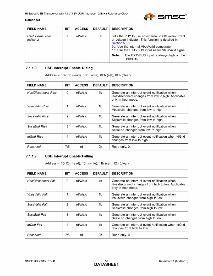
Hi-Speed USB Transceiver with 1.8V-3.3V ULPI Interface - 24MHz Reference Clock
Datasheet
7.1.1.8 USB Interrupt Enable Rising
Address = 0D-0Fh (read), 0Dh (write), 0Eh (set), 0Fh (clear)
7.1.1.9 USB Interrupt Enable Falling
Address = 10-12h (read), 10h (write), 11h (set), 12h (clear)
UseExternalVbusIndicator
7 rd/w/s/c 0b Tells the PHY to use an external VBUS over-current or voltage indicator. This function is detailed in Section 5.6.2.0b: Use the internal VbusValid comparator1b: Use the EXTVBUS input as for VbusValid signal.
Note: The EXTVBUS input is always high on the USB3315.
FIELD NAME BIT ACCESS DEFAULT DESCRIPTION
HostDisconnect Rise 0 rd/w/s/c 1b Generate an interrupt event notification when Hostdisconnect changes from low to high. Applicable only in host mode.
VbusValid Rise 1 rd/w/s/c 1b Generate an interrupt event notification when Vbusvalid changes from low to high.
SessValid Rise 2 rd/w/s/c 1b Generate an interrupt event notification when SessValid changes from low to high.
SessEnd Rise 3 rd/w/s/c 1b Generate an interrupt event notification when SessEnd changes from low to high.
IdGnd Rise 4 rd/w/s/c 1b Generate an interrupt event notification when IdGnd changes from low to high.
Reserved 7:5 rd 0h Read only, 0.
FIELD NAME BIT ACCESS DEFAULT DESCRIPTION
HostDisconnect Fall 0 rd/w/s/c 1b Generate an interrupt event notification when Hostdisconnect changes from high to low. Applicable only in host mode.
VbusValid Fall 1 rd/w/s/c 1b Generate an interrupt event notification when Vbusvalid changes from high to low.
SessValid Fall 2 rd/w/s/c 1b Generate an interrupt event notification when SessValid changes from high to low.
SessEnd Fall 3 rd/w/s/c 1b Generate an interrupt event notification when SessEnd changes from high to low.
IdGnd Fall 4 rd/w/s/c 1b Generate an interrupt event notification when IdGnd changes from high to low.
Reserved 7:5 rd 0h Read only, 0.
FIELD NAME BIT ACCESS DEFAULT DESCRIPTION
SMSC USB3315 REV C 57 Revision 2.1 (06-02-10)DATASHEET
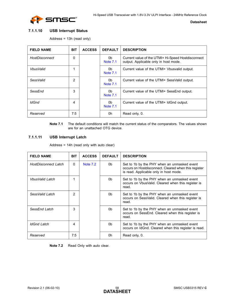
Hi-Speed USB Transceiver with 1.8V-3.3V ULPI Interface - 24MHz Reference Clock
Datasheet
7.1.1.10 USB Interrupt Status
Address = 13h (read only)
Note 7.1 The default conditions will match the current status of the comparators. The values shownare for an unattached OTG device.
7.1.1.11 USB Interrupt Latch
Address = 14h (read only with auto clear)
Note 7.2 Read Only with auto clear.
FIELD NAME BIT ACCESS DEFAULT DESCRIPTION
HostDisconnect 0 0bNote 7.1
Current value of the UTMI+ Hi-Speed Hostdisconnect output. Applicable only in host mode.
VbusValid 1 0bNote 7.1
Current value of the UTMI+ Vbusvalid output.
SessValid 2 0bNote 7.1
Current value of the UTMI+ SessValid output.
SessEnd 3 0bNote 7.1
Current value of the UTMI+ SessEnd output.
IdGnd 4 0bNote 7.1
Current value of the UTMI+ IdGnd output.
Reserved 7:5 0h Read only, 0.
FIELD NAME BIT ACCESS DEFAULT DESCRIPTION
HostDisconnect Latch 0 Note 7.2 0b Set to 1b by the PHY when an unmasked event occurs on Hostdisconnect. Cleared when this register is read. Applicable only in host mode.
VbusValid Latch 1 0b Set to 1b by the PHY when an unmasked event occurs on VbusValid. Cleared when this register is read.
SessValid Latch 2 0b Set to 1b by the PHY when an unmasked event occurs on SessValid. Cleared when this register is read.
SessEnd Latch 3 0b Set to 1b by the PHY when an unmasked event occurs on SessEnd. Cleared when this register is read.
IdGnd Latch 4 0b Set to 1b by the PHY when an unmasked event occurs on IdGnd. Cleared when this register is read.
Reserved 7:5 0h Read only, 0.
Revision 2.1 (06-02-10) 58 SMSC USB3315 REV CDATASHEET
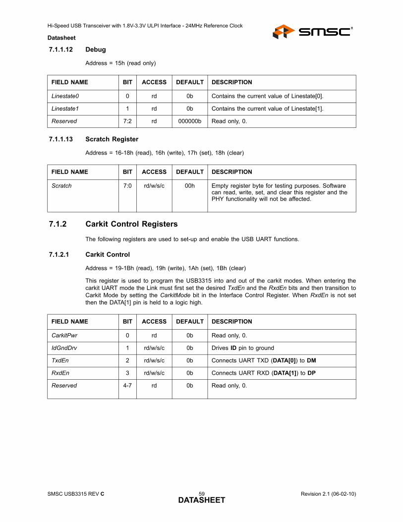
Hi-Speed USB Transceiver with 1.8V-3.3V ULPI Interface - 24MHz Reference Clock
Datasheet
7.1.1.12 Debug
Address = 15h (read only)
7.1.1.13 Scratch Register
Address = 16-18h (read), 16h (write), 17h (set), 18h (clear)
7.1.2 Carkit Control Registers
The following registers are used to set-up and enable the USB UART functions.
7.1.2.1 Carkit Control
Address = 19-1Bh (read), 19h (write), 1Ah (set), 1Bh (clear)
This register is used to program the USB3315 into and out of the carkit modes. When entering thecarkit UART mode the Link must first set the desired TxdEn and the RxdEn bits and then transition toCarkit Mode by setting the CarkitMode bit in the Interface Control Register. When RxdEn is not setthen the DATA[1] pin is held to a logic high.
FIELD NAME BIT ACCESS DEFAULT DESCRIPTION
Linestate0 0 rd 0b Contains the current value of Linestate[0].
Linestate1 1 rd 0b Contains the current value of Linestate[1].
Reserved 7:2 rd 000000b Read only, 0.
FIELD NAME BIT ACCESS DEFAULT DESCRIPTION
Scratch 7:0 rd/w/s/c 00h Empty register byte for testing purposes. Software can read, write, set, and clear this register and the PHY functionality will not be affected.
FIELD NAME BIT ACCESS DEFAULT DESCRIPTION
CarkitPwr 0 rd 0b Read only, 0.
IdGndDrv 1 rd/w/s/c 0b Drives ID pin to ground
TxdEn 2 rd/w/s/c 0b Connects UART TXD (DATA[0]) to DM
RxdEn 3 rd/w/s/c 0b Connects UART RXD (DATA[1]) to DP
Reserved 4-7 rd 0b Read only, 0.
SMSC USB3315 REV C 59 Revision 2.1 (06-02-10)DATASHEET
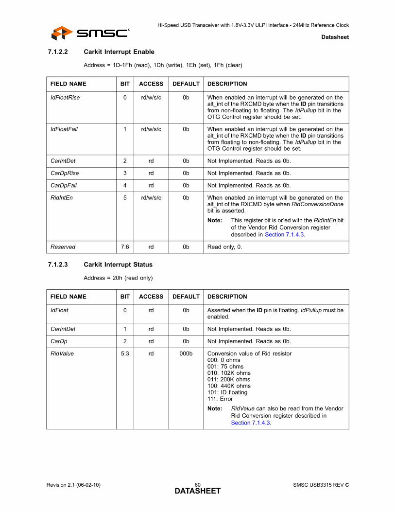
Hi-Speed USB Transceiver with 1.8V-3.3V ULPI Interface - 24MHz Reference Clock
Datasheet
7.1.2.2 Carkit Interrupt Enable
Address = 1D-1Fh (read), 1Dh (write), 1Eh (set), 1Fh (clear)
7.1.2.3 Carkit Interrupt Status
Address = 20h (read only)
FIELD NAME BIT ACCESS DEFAULT DESCRIPTION
IdFloatRise 0 rd/w/s/c 0b When enabled an interrupt will be generated on the alt_int of the RXCMD byte when the ID pin transitions from non-floating to floating. The IdPullup bit in the OTG Control register should be set.
IdFloatFall 1 rd/w/s/c 0b When enabled an interrupt will be generated on the alt_int of the RXCMD byte when the ID pin transitions from floating to non-floating. The IdPullup bit in the OTG Control register should be set.
CarIntDet 2 rd 0b Not Implemented. Reads as 0b.
CarDpRise 3 rd 0b Not Implemented. Reads as 0b.
CarDpFall 4 rd 0b Not Implemented. Reads as 0b.
RidIntEn 5 rd/w/s/c 0b When enabled an interrupt will be generated on the alt_int of the RXCMD byte when RidConversionDone bit is asserted.
Note: This register bit is or’ed with the RidIntEn bit of the Vendor Rid Conversion register described in Section 7.1.4.3.
Reserved 7:6 rd 0b Read only, 0.
FIELD NAME BIT ACCESS DEFAULT DESCRIPTION
IdFloat 0 rd 0b Asserted when the ID pin is floating. IdPullup must be enabled.
CarIntDet 1 rd 0b Not Implemented. Reads as 0b.
CarDp 2 rd 0b Not Implemented. Reads as 0b.
RidValue 5:3 rd 000b Conversion value of Rid resistor000: 0 ohms001: 75 ohms010: 102K ohms011: 200K ohms100: 440K ohms101: ID floating111: Error
Note: RidValue can also be read from the Vendor Rid Conversion register described in Section 7.1.4.3.
Revision 2.1 (06-02-10) 60 SMSC USB3315 REV CDATASHEET
Hi-Speed USB Transceiver with 1.8V-3.3V ULPI Interface - 24MHz Reference Clock
Datasheet
7.1.2.4 Carkit Interrupt Latch
Address = 21h (read only with auto-clear)
Note: rd*: Read Only with auto clear.
7.1.3 Extended Register Access
The USB3315 supports extended register access. The immediate register set (00-3Fh) can beaccessed through either a immediate address or an extended register address.
7.1.4 Vendor Register Access
The vendor specific registers include the range from 30h to 3Fh. These can be accessed by the ULPIimmediate register read / write.
RidConversionDone 6 rd 0b Automatically asserted by the USB3315 when the Rid Conversion is finished. The conversion will take 282uS. This bit will auto clear when the RidValue is read from the Rid Conversion Register. Reading the RidValue from the Carkit interrupt Status register will not clear either RidConversionDone status bit.
Note: RidConversionDone can also be read from the Vendor Rid Conversion register described in Section 7.1.4.3.
Reserved 7 rd 0b Read only, 0.
FIELD NAME BIT ACCESS DEFAULT DESCRIPTION
IdFloat Latch 0 rd* 0b Asserted if the state of the ID pin changes from non-floating to floating while the IdFloatRise bit is enabled or if the state of the ID pin changes from floating to non-floating while the IdFloatFall bit is enabled.
CarIntDet Latch 1 rd 0b Not Implemented. Reads as 0b.
CarDp Latch 2 rd 0b Not Implemented. Reads as 0b.
RidConversionLatch 3 rd* 0b If RidIntEn is set and the state of the RidConversionDone bit changes from a 0 to 1 this bit will be asserted.
Reserved rd 00000b Read only, 0.
FIELD NAME BIT ACCESS DEFAULT DESCRIPTION
SMSC USB3315 REV C 61 Revision 2.1 (06-02-10)DATASHEET
Hi-Speed USB Transceiver with 1.8V-3.3V ULPI Interface - 24MHz Reference Clock
Datasheet
7.1.4.1 HS TX Boost
Address = 31h (read / write)
7.1.4.2 Headset Audio Mode
Address = 33h (read / write)
7.1.4.3 Vendor Rid Conversion
Address = 36-38h (read), 36h (write), 37h (set), 38h (clear)
FIELD NAME BIT ACCESS DEFAULT DESCRIPTION
Reserved 4:0 rd 00000b Read only, 0.
Boost 6:5 rd/w 00b Sets the HS transmitter amplitude as described in Section 5.2.1.00b: Nominal01b: Reserved10b: Enables 7.4% increased drive strength11b: Enables 3.7% increased drive strength
Reserved 7 rd 0b Read only, 0.
FIELD NAME BIT ACCESS DEFAULT DESCRIPTION
HeadsetAudioEn 3:0 rd/w 0000b When this field is set to a value of 1010, the Headset Audio Mode is enabled as described in Section 6.6.
Reserved 7:4 rd 0h Read only, 0.
FIELD NAME BIT ACCESS DEFAULT DESCRIPTION
RidValue 2:0 rd/w 000b Conversion value of Rid resistor000: 0 ohms001: 75 ohms010: 100K ohms011: 200K ohms100: 440K ohms101: ID floating111: Error
Note: RidValue can also be read from the Carkit Interrupt Status register described in Section 7.1.2.3.
RidConversionDone 3 rd* 0b Automatically asserted by the USB3315 when the Rid Conversion is finished. The conversion will take 282uS. This bit will auto clear when the RidValue is read from the Rid Conversion Register. Reading the RidValue from the Carkit interrupt Status register will not clear either RidConversionDone status bit.
Note: RidConversionDone can also be read from the Carkit Interrupt Status register described in Section 7.1.2.3.
Revision 2.1 (06-02-10) 62 SMSC USB3315 REV CDATASHEET
Hi-Speed USB Transceiver with 1.8V-3.3V ULPI Interface - 24MHz Reference Clock
Datasheet
Note: rd*: Read Only with auto clear.
7.1.4.4 USB IO & Power Management
Address = 39-3Bh (read), 39h (write), 3Ah (set), 3Bh (clear)
RidConversionStart 4 rd/w/s/c 0b When this bit is asserted either through a register write or set, the Rid converter will read the value of the ID resistor. When the conversion is complete this bit will auto clear.
Reserved 5 rd/w/s/c 0b This bit must remain at 0.
RidIntEn 6 rd/w/s/c 0b When enabled an interrupt will be generated on the alt_int of the RXCMD byte when RidConversionDone bit is asserted.
Note: This register bit is or’ed with the RidIntEn bit of the Carkit Interrupt Status register.
Reserved 7 rd 0b Read only, 0.
FIELD NAME BIT ACCESS DEFAULT DESCRIPTION
Reserved 0 rd/w/s/c 0b Read only, 0.
SwapDP/DM 1 rd/w/s/c 0b When asserted, the DP and DM pins of the USB PHY are swapped. This bit can be used to prevent crossing the DP/DM traces on the board. In UART mode, it swaps the routing to the DP and DM pins.
UART RegOutput 3:2 rd/w/s/c 01b Controls the output voltage of the VBAT to VDD33 regulator in UART mode. When the PHY is switched from USB mode to UART mode regulator output will automatically change to the value specified in this register when TxdEn is asserted.00: 3.3V01: 3.0V (default)10: 2.75V11: 2.5V
ChargerPullupEnDP 4 rd/w/s/c 0b Enables a 125K Pull-up for USB Charger Detection when set on the DP pin. (The pull-up is automatically enabled in UART mode)
ChargerPullupEnDM 5 rd/w/s/c 0b Enables a 125K Pull-up for USB Charger Detection when set on the DM pin. (The pull-up is automatically enabled in UART mode)
USB RegOutput 7:6 rd/w/s/c 00b Controls the output voltage of the VBAT to VDD33 regulator in USB mode. When the PHY is in Synchronous Mode, Serial Mode, or Low Power Mode the regulator output will be the value specified in this register.00: 3.3V (default)01: 3.0V10: 2.75V11: 2.5V
FIELD NAME BIT ACCESS DEFAULT DESCRIPTION
SMSC USB3315 REV C 63 Revision 2.1 (06-02-10)DATASHEET
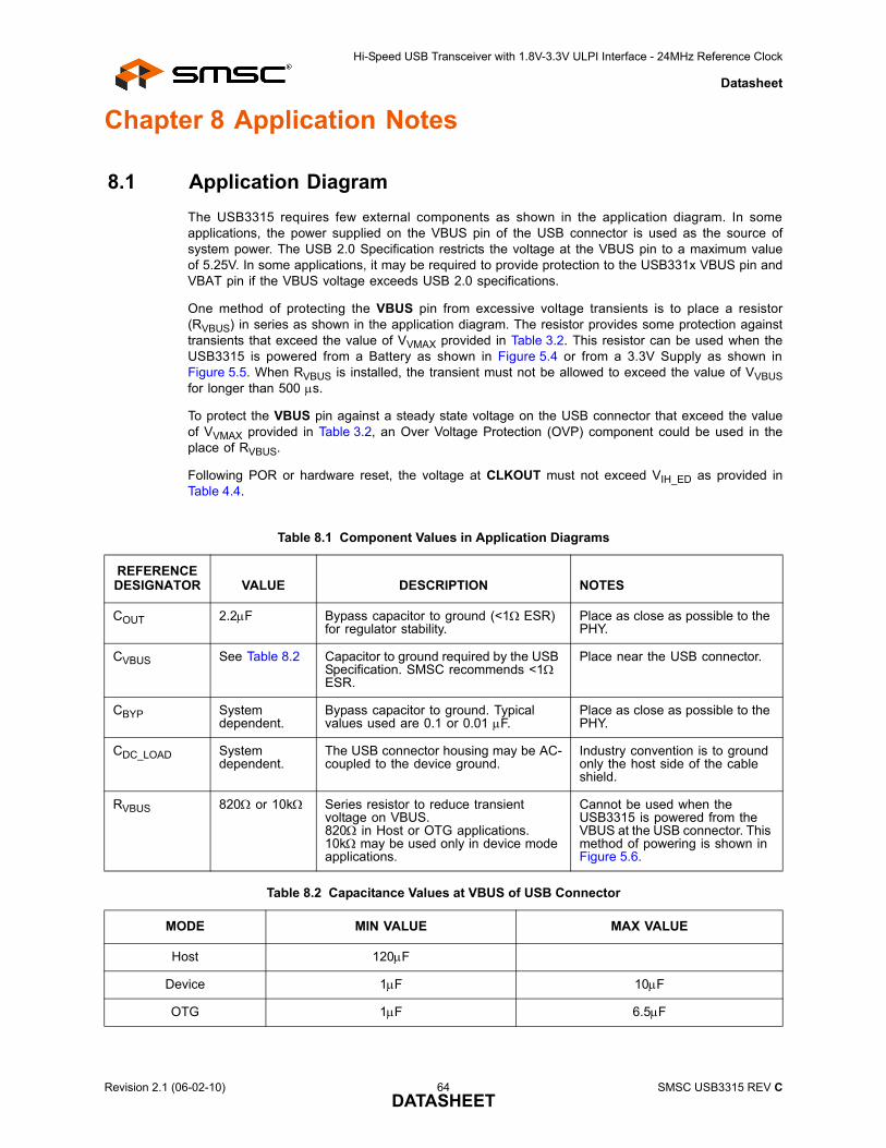
Hi-Speed USB Transceiver with 1.8V-3.3V ULPI Interface - 24MHz Reference Clock
Datasheet
Chapter 8 Application Notes
8.1 Application DiagramThe USB3315 requires few external components as shown in the application diagram. In someapplications, the power supplied on the VBUS pin of the USB connector is used as the source ofsystem power. The USB 2.0 Specification restricts the voltage at the VBUS pin to a maximum valueof 5.25V. In some applications, it may be required to provide protection to the USB331x VBUS pin andVBAT pin if the VBUS voltage exceeds USB 2.0 specifications.
One method of protecting the VBUS pin from excessive voltage transients is to place a resistor(RVBUS) in series as shown in the application diagram. The resistor provides some protection againsttransients that exceed the value of VVMAX provided in Table 3.2. This resistor can be used when theUSB3315 is powered from a Battery as shown in Figure 5.4 or from a 3.3V Supply as shown inFigure 5.5. When RVBUS is installed, the transient must not be allowed to exceed the value of VVBUSfor longer than 500 μs.
To protect the VBUS pin against a steady state voltage on the USB connector that exceed the valueof VVMAX provided in Table 3.2, an Over Voltage Protection (OVP) component could be used in theplace of RVBUS.
Following POR or hardware reset, the voltage at CLKOUT must not exceed VIH_ED as provided inTable 4.4.
Table 8.1 Component Values in Application Diagrams
REFERENCEDESIGNATOR VALUE DESCRIPTION NOTES
COUT 2.2μF Bypass capacitor to ground (<1Ω ESR) for regulator stability.
Place as close as possible to the PHY.
CVBUS See Table 8.2 Capacitor to ground required by the USB Specification. SMSC recommends <1Ω ESR.
Place near the USB connector.
CBYP System dependent.
Bypass capacitor to ground. Typical values used are 0.1 or 0.01 μF.
Place as close as possible to the PHY.
CDC_LOAD System dependent.
The USB connector housing may be AC-coupled to the device ground.
Industry convention is to ground only the host side of the cable shield.
RVBUS 820Ω or 10kΩ Series resistor to reduce transient voltage on VBUS.820Ω in Host or OTG applications.10kΩ may be used only in device mode applications.
Cannot be used when the USB3315 is powered from the VBUS at the USB connector. This method of powering is shown in Figure 5.6.
Table 8.2 Capacitance Values at VBUS of USB Connector
MODE MIN VALUE MAX VALUE
Host 120μF
Device 1μF 10μF
OTG 1μF 6.5μF
Revision 2.1 (06-02-10) 64 SMSC USB3315 REV CDATASHEET
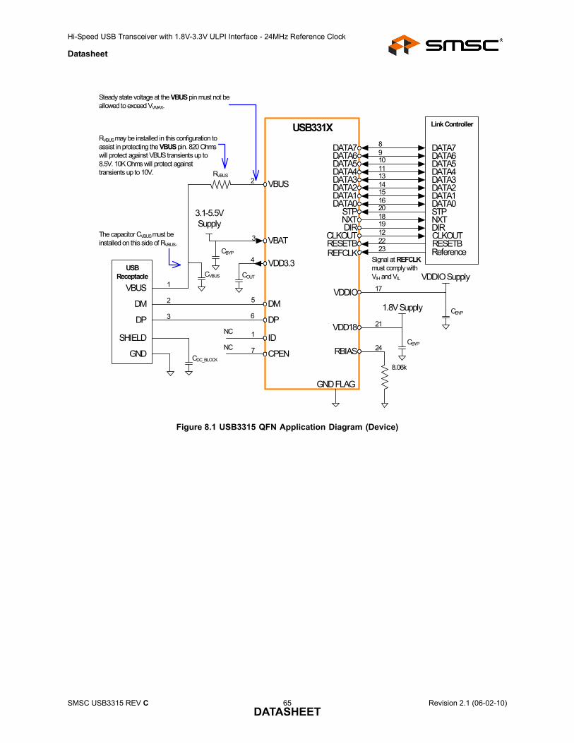
Hi-Speed USB Transceiver with 1.8V-3.3V ULPI Interface - 24MHz Reference Clock
Datasheet
Figure 8.1 USB3315 QFN Application Diagram (Device)
Link ControllerUSB331X
RBIAS
DIRNXTSTP
CLKOUT
DATA7DATA6DATA5DATA4DATA3DATA2
DATA0DATA1
VBAT
VDD3.3
VBUS
DM
DP
ID
RESETB
USB Receptacle
DM
DP
DIRNXTSTP
CLKOUT
DATA7DATA6DATA5DATA4DATA3DATA2
DATA0DATA1
RESETB
6
5
24
GND FLAG
2
3
VBUS 1
SHIELD
GND
4
3
2
1
CBYP
CVBUS
3.1-5.5VSupply
RVBUS may be installed in this configuration to assist in protecting the VBUS pin. 820 Ohms will protect against VBUS transients up to 8.5V. 10K Ohms will protect against transients up to 10V.
REFCLK
VDD18 21
Reference
COUT
CDC_BLOCK
8.06k
Steady state voltage at the VBUS pin must not be allowed to exceed VVMAX.
RVBUS
NC
89101113141516201819122223
CBYP
1.8V Supply
VDDIO 17
CBYP
VDDIO Supply
CPEN7NC
The capacitor CVBUS must be installed on this side of RVBUS.
Signal at REFCLK must comply with VIH and VIL
SMSC USB3315 REV C 65 Revision 2.1 (06-02-10)DATASHEET
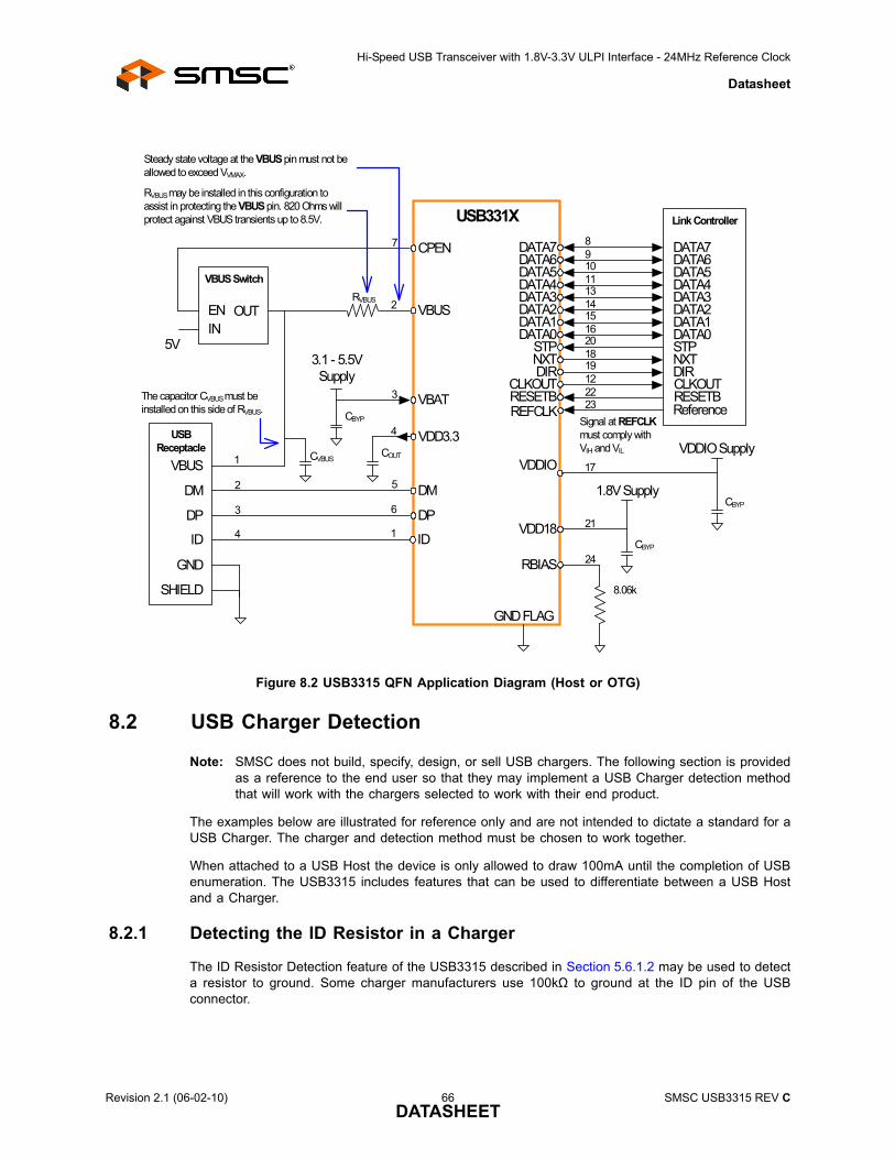
Hi-Speed USB Transceiver with 1.8V-3.3V ULPI Interface - 24MHz Reference Clock
Datasheet
8.2 USB Charger Detection
Note: SMSC does not build, specify, design, or sell USB chargers. The following section is providedas a reference to the end user so that they may implement a USB Charger detection methodthat will work with the chargers selected to work with their end product.
The examples below are illustrated for reference only and are not intended to dictate a standard for aUSB Charger. The charger and detection method must be chosen to work together.
When attached to a USB Host the device is only allowed to draw 100mA until the completion of USBenumeration. The USB3315 includes features that can be used to differentiate between a USB Hostand a Charger.
8.2.1 Detecting the ID Resistor in a Charger
The ID Resistor Detection feature of the USB3315 described in Section 5.6.1.2 may be used to detecta resistor to ground. Some charger manufacturers use 100kΩ to ground at the ID pin of the USBconnector.
Figure 8.2 USB3315 QFN Application Diagram (Host or OTG)
Link ControllerUSB331X
RBIAS
DIRNXTSTP
CLKOUT
DATA7DATA6DATA5DATA4DATA3DATA2
DATA0DATA1
REFCLK
VDD18
VBAT
VDD3.3
VBUS
DM
DP
RESETB
USB Receptacle
DM
DP
DIRNXTSTP
CLKOUT
DATA7DATA6DATA5DATA4DATA3DATA2
DATA0DATA1
RESETB
89
6
5
1011131415162018191222
21
23
24
1
GND FLAG
2
3
VBUS
GND
SHIELD
CVBUS
4
3
2
VDDIO 17
CPEN7
VBUS Switch
OUTEN
COUT
CBYP
IN
ID 4 ID1
3.1 - 5.5VSupply
CBYP
1.8V SupplyCBYP
VDDIO Supply
8.06k
Reference
5V
RVBUS may be installed in this configuration to assist in protecting the VBUS pin. 820 Ohms will protect against VBUS transients up to 8.5V.
RVBUS
The capacitor CVBUS must be installed on this side of RVBUS.
Steady state voltage at the VBUS pin must not be allowed to exceed VVMAX.
Signal at REFCLK must comply with VIH and VIL
Revision 2.1 (06-02-10) 66 SMSC USB3315 REV CDATASHEET
Hi-Speed USB Transceiver with 1.8V-3.3V ULPI Interface - 24MHz Reference Clock
Datasheet
Pseudo Algorithm for detecting resistor to ground and reading valueWait for IdGndEnable IdPullupSet RidConversionStartWait for RidConversionDoneRead RidValue
8.2.2 Detecting DP Shorted to DM
USB Chargers and USB Hosts will present 5V nominal onto the Vbus terminal of the USB connectorat all times. While in synchronous mode, the Link can detect SessVld in the RXCMD byte as shownin Table 6.3. In any of the non-synchronous modes, the Link must monitor the interrupt signal onDATA[3] as described in Table 6.4. When an interrupt occurs, the Link commands the USB3315 to exitLow Power Mode and reads registers to discover what caused the interrupt.
In preparation for testing if a charger has connected the DP and DM pins in the USB connector, theDP and DM pins of the USB3315 must be placed into Non-Driving, FS mode using the Full Speedtransceivers. This is done by writing 49h to the Function Control register at address 04h. Next, pull-upresistors can be enabled on the DP and DM pins. As described in Section 5.8, the pull-up resistorsmay be enabled individually. For example, setting bit 4 in the USB IO & Power Management registerat address 3Ah will connect the ChargerPullupEnableDP resistor. Likewise, a write to the USB IO &Power Management register at address 3Ah with a 20h will connect the ChargerPullupEnableDMresistor.
The linestate signals are monitored to determine whether the DP and DM pins are shorted. While insynchronous mode, the Link can monitor Linestate0 and Linestate1 in the RXCMD byte as shown inTable 6.3, or by reading the Debug register. In any of the non-synchronous modes, the Link canmonitor linestate on DATA[0] and DATA[1] as described in Table 6.3. The DC Electrical Characteristicsof the Single-Ended Receivers used to generate the linestate signals are provided in Table 4.6.
Pseudo Algorithm for detecting voltage at Vbus and detecting DP shorted to DMWait for SessVldTri-State DP/DM and select FS transceiversEnable ChargerPullupEnableDP resistorEnable ChargerPullupEnableDM resistorIf the linestates show a SE1 the charger has been detected. If the linestates show an SE0 you are connected to a host.
8.3 Reference DesignsSMSC has generated reference designs for connecting the USB3315 to SOCs with a ULPI port. Pleasecontact the SMSC sales office for more details.
8.4 ESD PerformanceThe USB3315 is protected from ESD strikes. By eliminating the requirement for external ESDprotection devices, board space is conserved, and the board manufacturer is enabled to reduce cost.The advanced ESD structures integrated into the USB3315 protect the device whether or not it ispowered up.
8.4.1 Human Body Model (HBM) Performance
HBM testing verifies the ability to withstand the ESD strikes like those that occur during handling andmanufacturing, and is done without power applied to the IC. To pass the test, the device must haveno change in operation or performance due to the event. All pins on the USB3315 except the REFCLKpin provide ±8kV HBM protection, as shown in Table 4.9.
SMSC USB3315 REV C 67 Revision 2.1 (06-02-10)DATASHEET
Hi-Speed USB Transceiver with 1.8V-3.3V ULPI Interface - 24MHz Reference Clock
Datasheet
8.4.2 EN/IEC 61000-4-2 Performance
The EN/IEC 61000-4-2 ESD specification is an international standard that addresses system-levelimmunity to ESD strikes while the end equipment is operational. In contrast, the HBM ESD tests areperformed at the device level with the device powered down.
SMSC contracts with Independent laboratories to test the USB3315 to EN/IEC 61000-4-2 in a workingsystem. Reports are available upon request. Please contact your SMSC representative, and requestinformation on 3rd party ESD test results. The reports show that systems designed with the USB3315can safely provide the ESD performance shown in Table 4.9 without additional board level protection.
In addition to defining the ESD tests, EN/IEC 61000-4-2 also categorizes the impact to equipmentoperation when the strike occurs (ESD Result Classification). The USB3315 maintains an ESD ResultClassification 1 or 2 when subjected to an EN/IEC 61000-4-2 (level 4) ESD strike.
Both air discharge and contact discharge test techniques for applying stress conditions are defined bythe EN/IEC 61000-4-2 ESD document.
8.4.3 Air Discharge
To perform this test, a charged electrode is moved close to the system being tested until a spark isgenerated. This test is difficult to reproduce because the discharge is influenced by such factors ashumidity, the speed of approach of the electrode, and construction of the test equipment.
8.4.4 Contact Discharge
The uncharged electrode first contacts the USB connector to prepare this test, and then the probe tipis energized. This yields more repeatable results, and is the preferred test method. The independenttest laboratories contracted by SMSC provide test results for both types of discharge methods.
Revision 2.1 (06-02-10) 68 SMSC USB3315 REV CDATASHEET
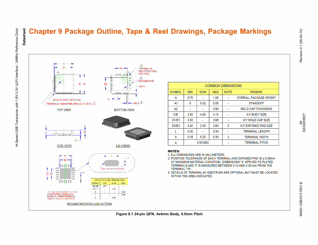
SM
SC
US
B33
15 R
EV C
69
Rev
isio
n 2.
1 (0
6-02
-10)
DAT
AS
HE
ET
Hi-S
peed
US
B Tr
ansc
eive
r with
1.8
V-3.
3V U
LPI I
nter
face
- 24
MH
z R
efer
ence
Clo
ck age Markings
Datas
heet Chapter 9 Package Outline, Tape & Reel Drawings, Pack
Figure 9.1 24-pin QFN, 4x4mm Body, 0.5mm Pitch
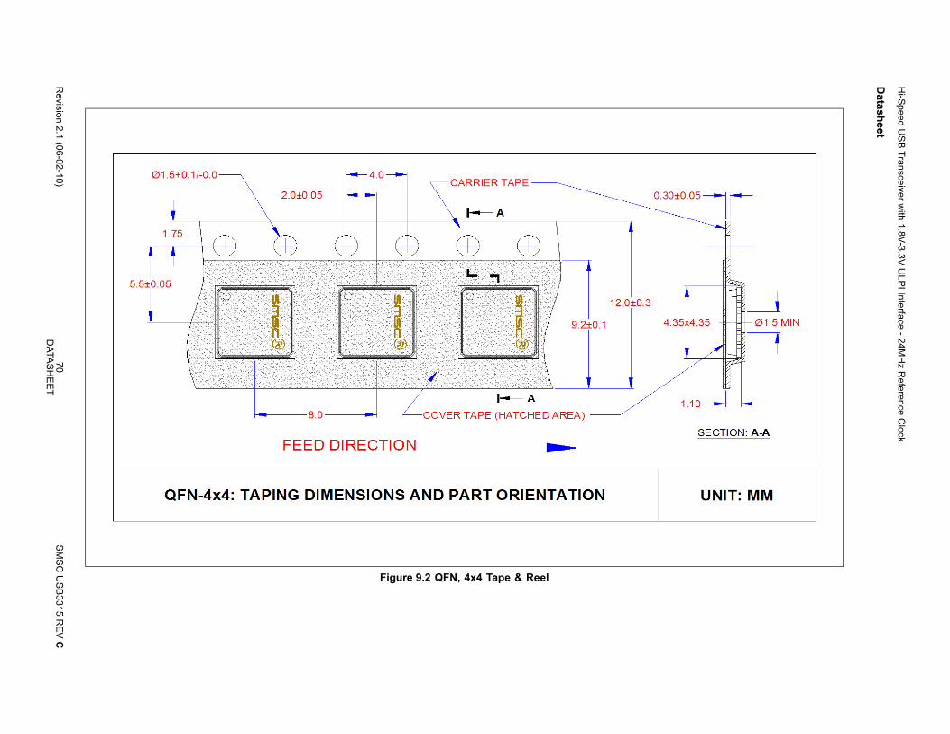
Hi-Speed U
SB
Transceiver with 1.8V-3.3V U
LPI Interface - 24M
Hz R
eference Clock
Datasheet
Revision 2.1 (06-02-10)
70 S
MS
C U
SB3315 R
EV
CD
ATAS
HE
ET
Figure 9.2 QFN, 4x4 Tape & Reel
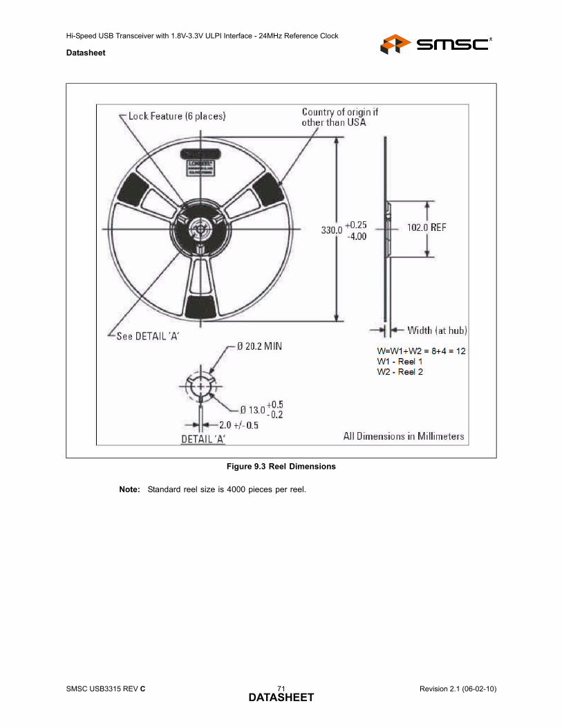
Hi-Speed USB Transceiver with 1.8V-3.3V ULPI Interface - 24MHz Reference Clock
Datasheet
Note: Standard reel size is 4000 pieces per reel.
Figure 9.3 Reel Dimensions
SMSC USB3315 REV C 71 Revision 2.1 (06-02-10)DATASHEET
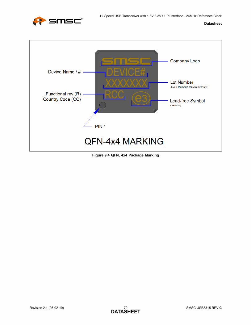
Hi-Speed USB Transceiver with 1.8V-3.3V ULPI Interface - 24MHz Reference Clock
Datasheet
Figure 9.4 QFN, 4x4 Package Marking
Revision 2.1 (06-02-10) 72 SMSC USB3315 REV CDATASHEET
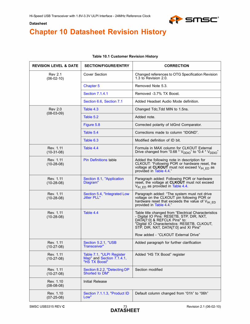
Hi-Speed USB Transceiver with 1.8V-3.3V ULPI Interface - 24MHz Reference Clock
Datasheet
Chapter 10 Datasheet Revision History
Table 10.1 Customer Revision History
REVISION LEVEL & DATE SECTION/FIGURE/ENTRY CORRECTION
Rev 2.1(06-02-10)
Cover Section Changed references to OTG Specification Revision 1.3 to Revision 2.0.
Chapter 5 Removed Note 5.3.
Section 7.1.4.1 Removed -3.7% TX Boost.
Section 6.6, Section 7.1 Added Headset Audio Mode definition.
Rev 2.0(08-03-09)
Table 4.3 Changed Tdc,Tdd MIN to 1.5ns.
Table 5.2 Added note.
Figure 5.8 Corrected polarity of IdGnd Comparator.
Table 5.4 Corrections made to column “IDGND”.
Table 6.3 Modified definition of ID bit.
Rev. 1.11(10-31-08)
Table 4.4 Formula in MAX column for CLKOUT External Drive changed from “0.68 * VDDIO“ to “0.4 * VDDIO”
Rev. 1.11(10-28-08)
Pin Definitions table Added the following note in description for CLKOUT: “Following POR or hardware reset, the voltage at CLKOUT must not exceed VIH_ED as provided in Table 4.4.”
Rev. 1.11(10-28-08)
Section 8.1, "Application Diagram"
Paragraph added: Following POR or hardware reset, the voltage at CLKOUT must not exceed VIH_ED as provided in Table 4.4.
Rev. 1.11(10-28-08)
Section 5.4, "Integrated Low Jitter PLL"
Paragraph added: “The system must not drive voltage on the CLKOUT pin following POR or hardware reset that exceeds the value of VIH_ED provided in Table 4.4.”
Rev. 1.11(10-28-08)
Table 4.4 Table title changed from “Electrical Characteristics - Digital IO Pins: RESETB, STP, DIR, NXT, DATA[7:0] & REFCLK Pins" to:"Digital IO Characteristics: RESETB, CLKOUT, STP, DIR, NXT, DATA[7:0] and XI Pins"
Row added - “CLKOUT External Drive”
Rev. 1.11(10-27-08)
Section 5.2.1, "USB Transceiver"
Added paragraph for further clarification
Rev. 1.11(10-27-08)
Table 7.1, "ULPI Register Map" and Section 7.1.4.1, "HS TX Boost"
Added “HS TX Boost” register
Rev. 1.11(10-27-08)
Section 8.2.2, "Detecting DP Shorted to DM"
Section modified
Rev. 1.10(08-08-08)
Initial Release
Rev. 1.10(07-25-08)
Section 7.1.1.3, "Product ID Low"
Default column changed from “01h” to “06h”
SMSC USB3315 REV C 73 Revision 2.1 (06-02-10)DATASHEET
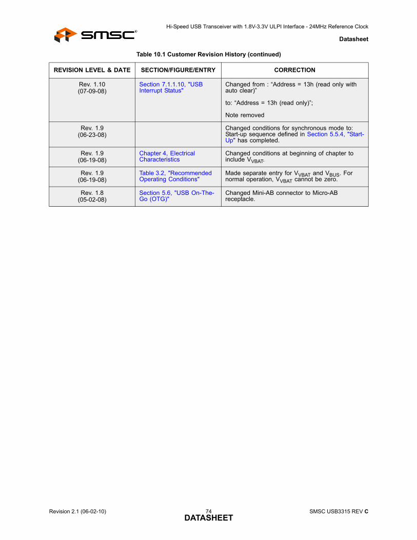
Hi-Speed USB Transceiver with 1.8V-3.3V ULPI Interface - 24MHz Reference Clock
Datasheet
Rev. 1.10(07-09-08)
Section 7.1.1.10, "USB Interrupt Status"
Changed from : “Address = 13h (read only with auto clear)”
to: “Address = 13h (read only)”;
Note removed
Rev. 1.9(06-23-08)
Changed conditions for synchronous mode to: Start-up sequence defined in Section 5.5.4, "Start-Up" has completed.
Rev. 1.9(06-19-08)
Chapter 4, Electrical Characteristics
Changed conditions at beginning of chapter to include VVBAT.
Rev. 1.9(06-19-08)
Table 3.2, "Recommended Operating Conditions"
Made separate entry for VVBAT and VBUS. For normal operation, VVBAT cannot be zero.
Rev. 1.8(05-02-08)
Section 5.6, "USB On-The-Go (OTG)"
Changed Mini-AB connector to Micro-AB receptacle.
Table 10.1 Customer Revision History (continued)
REVISION LEVEL & DATE SECTION/FIGURE/ENTRY CORRECTION
Revision 2.1 (06-02-10) 74 SMSC USB3315 REV CDATASHEET