usb 2.0 hi-speed 7-port hub...
TRANSCRIPT

USB2517/USB2517I
USB 2.0 Hi-Speed 7-Port Hub Controller
General Description
The 7-Port Hub is a low power, OEM configurable, MTT(multi transaction translator) hub controller IC with 7downstream ports for embedded USB solutions. The 7-port hub is fully compliant with the USB 2.0 Specifica-tion and will attach to an upstream port as a Full-SpeedHub or as a Full-/Hi-Speed Hub. The 7-Port Hub sup-ports Low-Speed, Full-Speed, and Hi-Speed (if operat-ing as a Hi-Speed Hub) downstream devices on all ofthe enabled downstream ports.
General Features
• Hub Controller IC with 7 downstream ports
• High-performance multiple transaction translator MultiTRAK™ Technology provides one transac-tion translator per port
• Enhanced OEM configuration options available through either a single serial I2C EEPROM, or SMBus Slave Port
• 64-Pin (9x9 mm) QFN, RoHS compliant package
• Supports commercial (0ºC to +70ºC) and indus-trial (-40ºC to +85ºC) temperature ranges
Hardware Features
• Low power operation
• Full Power Management with individual or ganged power control of each downstream port
• On-chip Power On Reset (POR)
• Internal 1.8V Voltage Regulator
• Fully integrated USB termination and Pull-up/Pull-down resistors
• On Board 24MHz Crystal Driver, Resonator, or External 24/MHz clock input
• USB host/device speed indicator. Per-port 3-color LED drivers indicate the speed of USB host and device connection - hi-speed (480 Mbps), full-speed (12 Mbps), low-speed (1.5 Mbps)
• Enhanced EMI rejection and ESD protection per-formance
OEM Selectable Features
• Customizable Vendor ID, Product ID, and Device ID
• Select whether the hub is part of a compound device (When any downstream port is perma-nently hardwired to a USB peripheral device, the hub is part of a compound device.)
• Flexible port mapping and disable sequence. Ports can be disabled/reordered in any order to support multiple product SKUs. Hub will automati-cally reorder the remaining ports to match the Host controller's numbering scheme
• Programmable USB differential-pair pin location
- Eases PCB layout by aligning USB signal lines directly to connectors
• Programmable USB signal drive strength. Recover USB signal integrity due to compromised system environments using 4-level driving strength resolution
• Select the presence of a permanently hardwired USB peripheral device on a port by port basis
• Configure the delay time for filtering the over-cur-rent sense inputs
• Configure the delay time for turning on down-stream port power
• Indicate the maximum current that the 347-port hub consumes from the USB upstream port
• Indicate the maximum current required for the hub controller
• Support Custom String Descriptor up to 31 char-acters in length for:
- Product String
- Manufacturer String
- Serial Number String
• Pin Selectable Options for Default Configuration
- Select Downstream Ports as Non-Removable Ports
- Select Downstream Ports as Disabled Ports
- Select Downstream Port Power Control and Over-Current Detection on a Ganged or Indi-vidual Basis
- Select USB Signal Drive Strength
- Select USB Differential Pair Pin location
2013-2018 Microchip Technology Inc. DS00001598C-page 1
USB2517/USB2517I
Applications
• LCD monitors and TVs
• Multi-function USB peripherals
• PC mother boards
• Set-top boxes, DVD players, DVR/PVR
• Printers and scanners
• PC media drive bay
• Portable hub boxes
• Mobile PC docking
• Embedded systems
DS00001598C-page 2 2013-2018 Microchip Technology Inc.
USB2517/USB2517I
TO OUR VALUED CUSTOMERS
It is our intention to provide our valued customers with the best documentation possible to ensure successful use of your Microchipproducts. To this end, we will continue to improve our publications to better suit your needs. Our publications will be refined andenhanced as new volumes and updates are introduced.
If you have any questions or comments regarding this publication, please contact the Marketing Communications Department viaE-mail at [email protected]. We welcome your feedback.
Most Current Data SheetTo obtain the most up-to-date version of this data sheet, please register at our Worldwide Web site at:
http://www.microchip.com
You can determine the version of a data sheet by examining its literature number found on the bottom outside corner of any page.
The last character of the literature number is the version number, (e.g., DS30000000A is version A of document DS30000000).
ErrataAn errata sheet, describing minor operational differences from the data sheet and recommended workarounds, may exist for cur-
rent devices. As device/documentation issues become known to us, we will publish an errata sheet. The errata will specify the
revision of silicon and revision of document to which it applies.
To determine if an errata sheet exists for a particular device, please check with one of the following:
• Microchip’s Worldwide Web site; http://www.microchip.com• Your local Microchip sales office (see last page)
When contacting a sales office, please specify which device, revision of silicon and data sheet (include -literature number) you areusing.
Customer Notification SystemRegister on our web site at www.microchip.com to receive the most current information on all of our products.
2013-2018 Microchip Technology Inc. DS00001598C-page 3
USB2517/USB2517I
DS00001598C-page 4 2013-2018 Microchip Technology Inc.
Table of Contents
1.0 Acronyms & Definitions ................................................................................................................................................................... 52.0 Block Diagram ................................................................................................................................................................................. 63.0 Pin Configuration ............................................................................................................................................................................. 74.0 Pin Table ......................................................................................................................................................................................... 85.0 Pin Descriptions and Buffer Type Descriptions ............................................................................................................................. 106.0 LED Usage Description ................................................................................................................................................................. 177.0 Configuration Options ................................................................................................................................................................... 198.0 DC Parameters ............................................................................................................................................................................. 479.0 AC Specifications .......................................................................................................................................................................... 5210.0 Package outline ........................................................................................................................................................................... 53Appendix A: Data Sheet Revision History ........................................................................................................................................... 55The Microchip Web Site ...................................................................................................................................................................... 56Customer Change Notification Service ............................................................................................................................................... 56Customer Support ............................................................................................................................................................................... 56Product Identification System .............................................................................................................................................................. 57
2013-2018 Microchip Technology Inc. DS00001598C-page 5
USB2517/USB2517I
1.0 ACRONYMS & DEFINITIONS
EEPROMM: Electrically Erasable Programmable Read-Only Memory (a type of non-volatile memory)
EMI: Electromagnetic Interference
ESD: Electrostatic Discharge
I2C: Inter-Integrated Circuit
LCD: Liquid Crystal Display
LED: Light Emitting Diode
OCS: Over-current sense
PCB: Printed Circuit Board
PHY: Physical Layer
PLL: Phase-Locked Loop
PVR: Personal Video Recorder (also known as a Digital Video Recorder)
QFN: Quad Flat No Leads
RoHS: Restriction of Hazardous Substances Directive
SCK: Serial Clock
SD: Secure Digital
SIE: Serial Interface Engine
SMBus: System Management Bus
TT: Transaction Translator
USB2517/USB2517I
DS00001598C-page 6 2013-2018 Microchip Technology Inc.
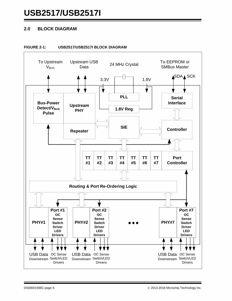
2.0 BLOCK DIAGRAM
FIGURE 2-1: USB2517/USB2517I BLOCK DIAGRAM
To UpstreamVBUS
3.3V
Upstream PHY
Upstream USB Data
Repeater ControllerSIE
Serial Interface
PLL
24 MHz CrystalTo EEPROM or SMBus Master
Routing & Port Re-Ordering Logic
SCKSDA
TT#7
Port Controller
PHY#1
Port #1OC
SenseSwitch DriverLED
Drivers
USB DataDownstream
OC SenseSwitch/LED
Drivers
Bus-Power Detect/VBUS
Pulse
1.8V
TT#6
TT#5
TT#1
1.8V Reg
PHY#2
Port #2OC
SenseSwitch DriverLED
Drivers
PHY#7
Port #7OC
SenseSwitch DriverLED
Drivers
USB DataDownstream
OC SenseSwitch/LED
Drivers
USB DataDownstream
OC SenseSwitch/LED
Drivers
TT#4
TT#3
TT#2
2013-2018 Microchip Technology Inc. DS00001598C-page 7
USB2517/USB2517I
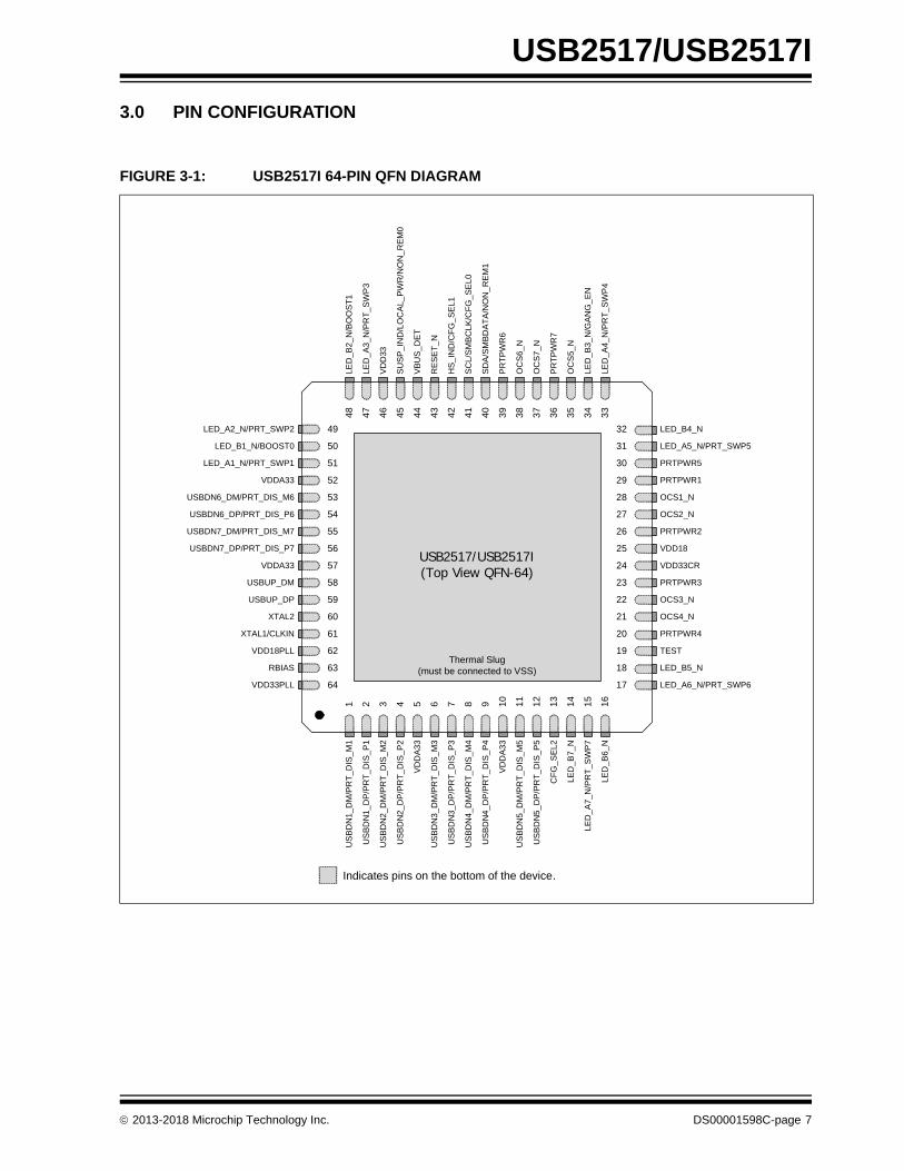
3.0 PIN CONFIGURATION
FIGURE 3-1: USB2517I 64-PIN QFN DIAGRAM
Thermal Slug(must be connected to VSS)
USB2517/USB2517I(Top View QFN-64)
Indicates pins on the bottom of the device.
USBDN6_DP/PRT_DIS_P6 54
USBDN7_DM/PRT_DIS_M7 55
USBDN6_DM/PRT_DIS_M6 53
USBDN7_DP/PRT_DIS_P7 56
VDDA33 57
USBUP_DP 59
XTAL2 60
XTAL1/CLKIN 61
RBIAS
64VDD33PLL
63
VDD18PLL 62
USBUP_DM 58
VD
DA
33
1U
SB
DN
1_
DM
/PR
T_
DIS
_M1
2U
SB
DN
1_
DP
/PR
T_
DIS
_P1
3U
SB
DN
2_
DM
/PR
T_
DIS
_M2
4U
SB
DN
2_
DP
/PR
T_
DIS
_P2
5
US
BD
N3
_D
M/P
RT
_D
IS_M
36
US
BD
N3
_D
P/P
RT
_D
IS_P
37
US
BD
N4
_D
M/P
RT
_D
IS_M
48
US
BD
N4
_D
P/P
RT
_D
IS_P
49
US
BD
N5
_D
P/P
RT
_D
IS_P
5
10
US
BD
N5
_D
M/P
RT
_D
IS_M
511
VD
DA
33
12
27 OCS2_N
26 PRTPWR2
25 VDD18
24 VDD33CR
23
OCS4_N
22
PRTPWR3
21
OCS3_N
20 PRTPWR4
19 TEST
29 PRTPWR1
28 OCS1_N
30 PRTPWR5
45
VD
D33
44
SU
SP
_IN
D/L
OC
AL_
PW
R/N
ON
_R
EM
0
43
VB
US
_DE
T
42
HS
_IN
D/C
FG
_S
EL
1
41
SC
L/S
MB
CL
K/C
FG
_SE
L0
40
SD
A/S
MB
DA
TA
/NO
N_
RE
M1
39
PR
TP
WR
6
38
OC
S6
_N
46
RE
SE
T_
N
37
OC
S7
_N
36
PR
TP
WR
7
35
OC
S5
_N
LED_B1_N/BOOST0 50
LED_A1_N/PRT_SWP1 51
LED_A2_N/PRT_SWP2 49
VDDA33 52
47
LED
_B2
_N/B
OO
ST
1
LED
_A3
_N/P
RT
_S
WP
3
48
33
LED
_B3
_N/G
AN
G_
EN
LED
_A4
_N/P
RT
_S
WP
4
34
18 LED_B5_N
17 LED_A6_N/PRT_SWP6
32 LED_B4_N
31 LED_A5_N/PRT_SWP5
CF
G_
SE
L213
LED
_B6
_N
14
LED
_A
7_N
/PR
T_S
WP
715
LED
_B7
_N
16
USB2517/USB2517I
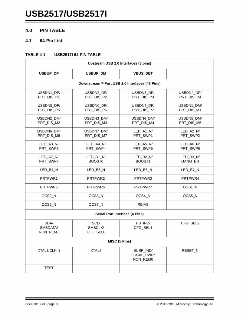
4.0 PIN TABLE
4.1 64-Pin List
TABLE 4-1: USB2517I 64-PIN TABLE
Upstream USB 2.0 Interfaces (3 pins)
USBUP_DP USBUP_DM VBUS_DET
Downstream 7-Port USB 2.0 Interfaces (43 Pins)
USBDN1_DP/PRT_DIS_P1
USBDN2_DP/PRT_DIS_P2
USBDN3_DP/PRT_DIS_P3
USBDN4_DP/PRT_DIS_P4
USBDN5_DP/PRT_DIS_P5
USBDN6_DP/PRT_DIS_P6
USBDN7_DP/PRT_DIS_P7
USBDN1_DM/PRT_DIS_M1
USBDN2_DM/PRT_DIS_M2
USBDN3_DM/PRT_DIS_M3
USBDN4_DM/PRT_DIS_M4
USBDN5_DM/PRT_DIS_M5
USBDN6_DM/PRT_DIS_M6
USBDN7_DM/PRT_DIS_M7
LED_A1_N/PRT_SWP1
LED_A2_N/PRT_SWP2
LED_A3_N/PRT_SWP3
LED_A4_N/PRT_SWP4
LED_A5_N/PRT_SWP5
LED_A6_N/PRT_SWP6
LED_A7_N/PRT_SWP7
LED_B1_N/BOOST0
LED_B2_N/BOOST1
LED_B3_N/GANG_EN
LED_B4_N LED_B5_N LED_B6_N LED_B7_N
PRTPWR1 PRTPWR2 PRTPWR3 PRTPWR4
PRTPWR5 PRTPWR6 PRTPWR7 OCS1_N
OCS2_N OCS3_N OCS4_N OCS5_N
OCS6_N OCS7_N RBIAS
Serial Port Interface (4 Pins)
SDA/SMBDATA/
NON_REM1
SCL/SMBCLK/
CFG_SEL0
HS_IND/CFG_SEL1
CFG_SEL2
MISC (5 Pins)
XTAL1/CLKIN XTAL2 SUSP_IND/LOCAL_PWR/NON_REM0
RESET_N
TEST
DS00001598C-page 8 2013-2018 Microchip Technology Inc.
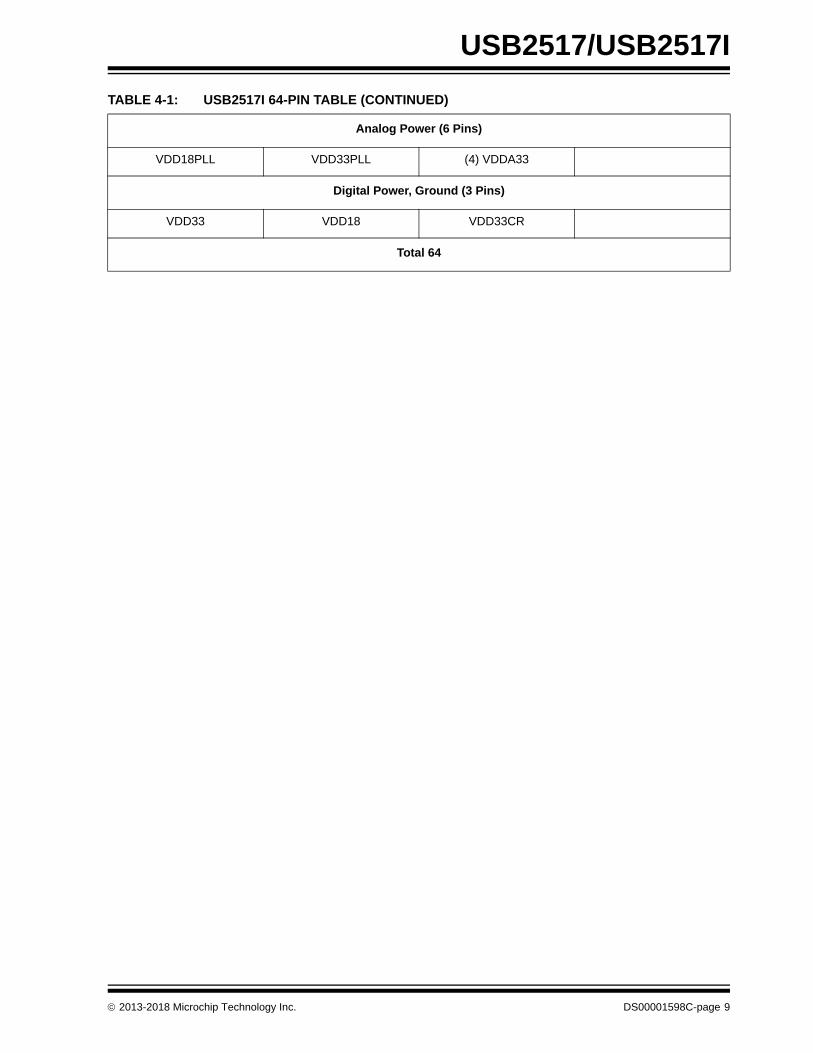
USB2517/USB2517I
Analog Power (6 Pins)
VDD18PLL VDD33PLL (4) VDDA33
Digital Power, Ground (3 Pins)
VDD33 VDD18 VDD33CR
Total 64
TABLE 4-1: USB2517I 64-PIN TABLE (CONTINUED)
2013-2018 Microchip Technology Inc. DS00001598C-page 9
USB2517/USB2517I
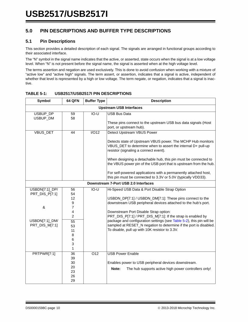
5.0 PIN DESCRIPTIONS AND BUFFER TYPE DESCRIPTIONS
5.1 Pin Descriptions
This section provides a detailed description of each signal. The signals are arranged in functional groups according totheir associated interface.
The “N” symbol in the signal name indicates that the active, or asserted, state occurs when the signal is at a low voltagelevel. When “N” is not present before the signal name, the signal is asserted when at the high voltage level.
The terms assertion and negation are used exclusively. This is done to avoid confusion when working with a mixture of“active low” and “active high” signals. The term assert, or assertion, indicates that a signal is active, independent ofwhether that level is represented by a high or low voltage. The term negate, or negation, indicates that a signal is inac-tive.
TABLE 5-1: USB2517/USB2517I PIN DESCRIPTIONS
Symbol 64 QFN Buffer Type Description
Upstream USB Interfaces
USBUP_DPUSBUP_DM
5958
IO-U USB Bus Data
These pins connect to the upstream USB bus data signals (Host port, or upstream hub).
VBUS_DET 44 I/O12 Detect Upstream VBUS Power
Detects state of Upstream VBUS power. The MCHP Hub monitors VBUS_DET to determine when to assert the internal D+ pull-up resistor (signaling a connect event).
When designing a detachable hub, this pin must be connected to the VBUS power pin of the USB port that is upstream from the hub.
For self-powered applications with a permanently attached host, this pin must be connected to 3.3V or 5.0V (typically VDD33).
Downstream 7-Port USB 2.0 Interfaces
USBDN[7:1]_DP/PRT_DIS_P[7:1]
&
USBDN[7:1]_DM/PRT_DIS_M[7:1]
5654129742
IO-U Hi-Speed USB Data & Port Disable Strap Option
USBDN_DP[7:1] / USBDN_DM[7:1]: These pins connect to the downstream USB peripheral devices attached to the hub’s port.
Downstream Port Disable Strap option:PRT_DIS_P[7:1] / PRT_DIS_M[7:1]: If the strap is enabled by package and configuration settings (see Table 5-2), this pin will be sampled at RESET_N negation to determine if the port is disabled.To disable, pull up with 10K resistor to 3.3V.
5553118631
PRTPWR[7:1] 36393020232629
O12 USB Power Enable
Enables power to USB peripheral devices downstream.
Note: The hub supports active high power controllers only!
DS00001598C-page 10 2013-2018 Microchip Technology Inc.
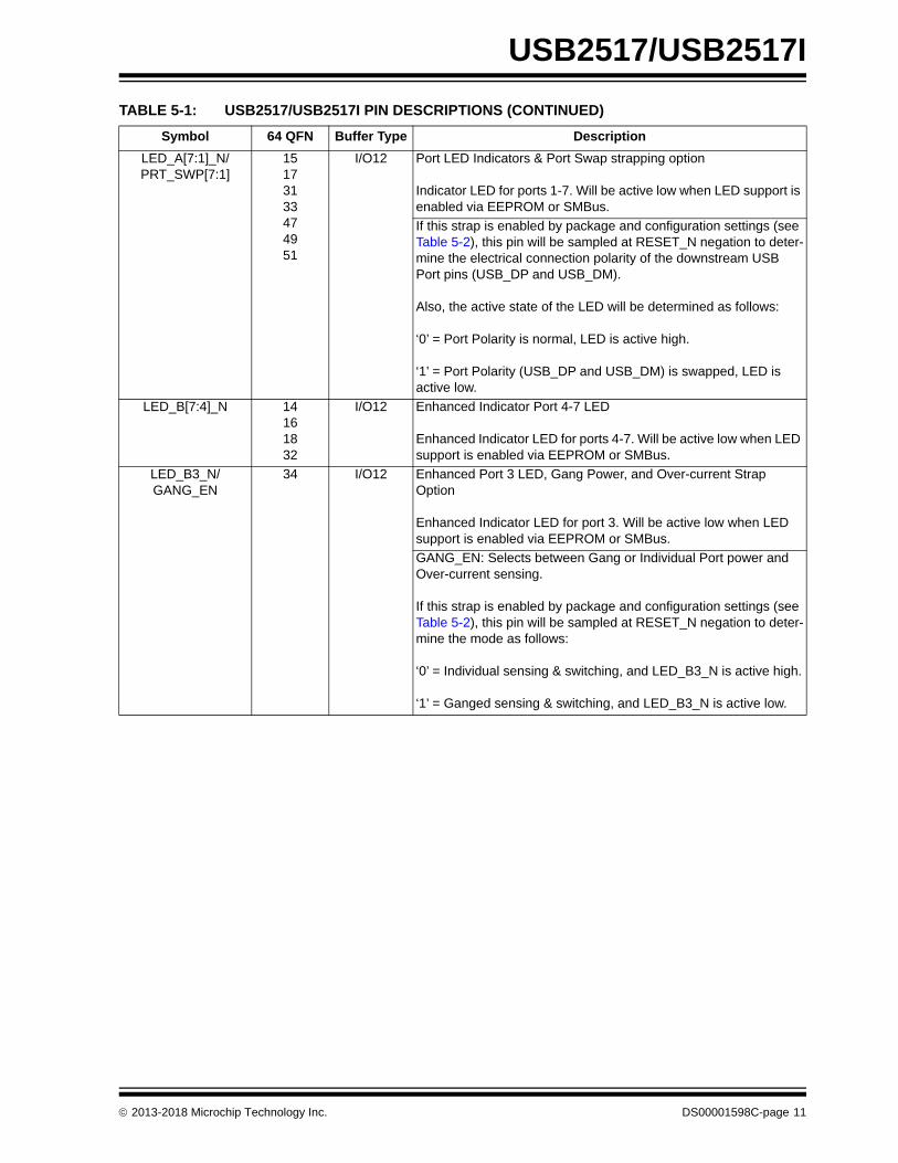
USB2517/USB2517I
LED_A[7:1]_N/PRT_SWP[7:1]
15173133474951
I/O12 Port LED Indicators & Port Swap strapping option
Indicator LED for ports 1-7. Will be active low when LED support is enabled via EEPROM or SMBus.
If this strap is enabled by package and configuration settings (see Table 5-2), this pin will be sampled at RESET_N negation to deter-mine the electrical connection polarity of the downstream USB Port pins (USB_DP and USB_DM).
Also, the active state of the LED will be determined as follows:
‘0’ = Port Polarity is normal, LED is active high.
‘1’ = Port Polarity (USB_DP and USB_DM) is swapped, LED is active low.
LED_B[7:4]_N 14161832
I/O12 Enhanced Indicator Port 4-7 LED
Enhanced Indicator LED for ports 4-7. Will be active low when LED support is enabled via EEPROM or SMBus.
LED_B3_N/GANG_EN
34 I/O12 Enhanced Port 3 LED, Gang Power, and Over-current Strap Option
Enhanced Indicator LED for port 3. Will be active low when LED support is enabled via EEPROM or SMBus.
GANG_EN: Selects between Gang or Individual Port power and Over-current sensing.
If this strap is enabled by package and configuration settings (see Table 5-2), this pin will be sampled at RESET_N negation to deter-mine the mode as follows:
‘0’ = Individual sensing & switching, and LED_B3_N is active high.
‘1’ = Ganged sensing & switching, and LED_B3_N is active low.
TABLE 5-1: USB2517/USB2517I PIN DESCRIPTIONS (CONTINUED)
Symbol 64 QFN Buffer Type Description
2013-2018 Microchip Technology Inc. DS00001598C-page 11
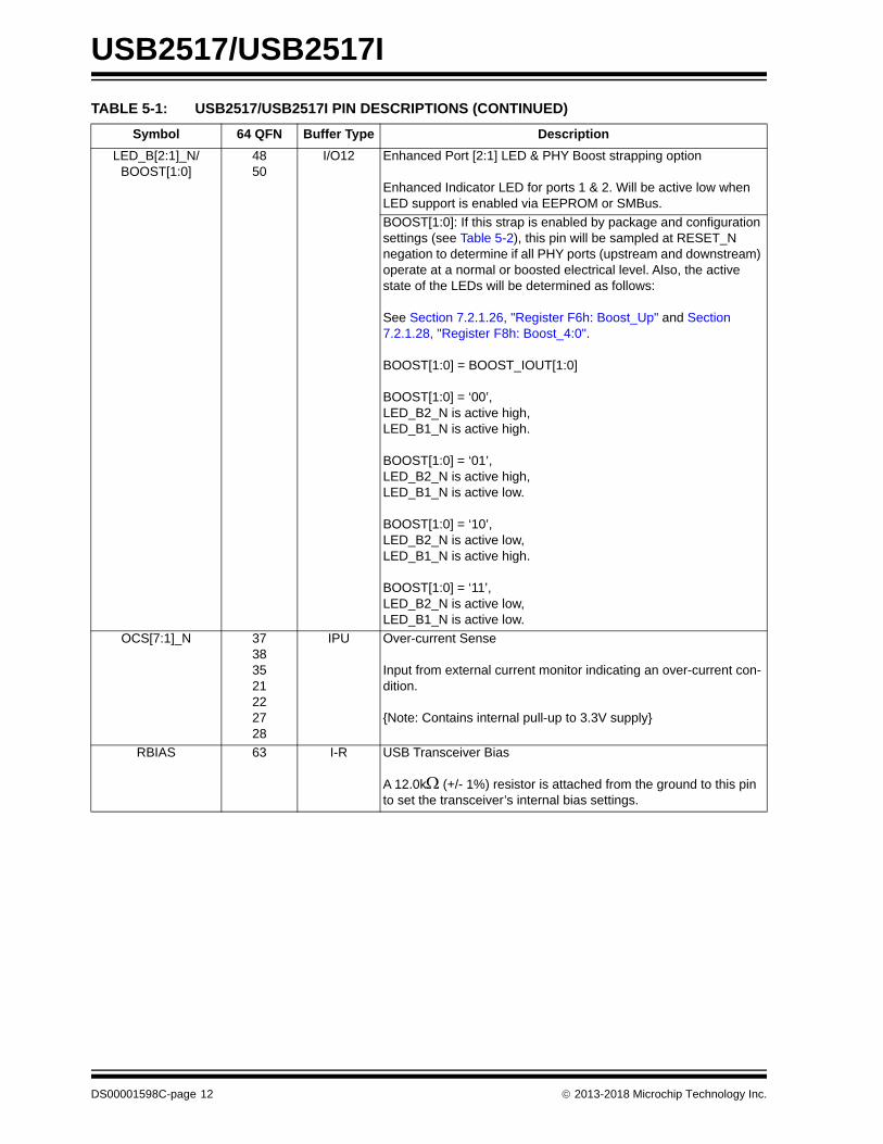
USB2517/USB2517I
LED_B[2:1]_N/BOOST[1:0]
4850
I/O12 Enhanced Port [2:1] LED & PHY Boost strapping option
Enhanced Indicator LED for ports 1 & 2. Will be active low when LED support is enabled via EEPROM or SMBus.
BOOST[1:0]: If this strap is enabled by package and configuration settings (see Table 5-2), this pin will be sampled at RESET_N negation to determine if all PHY ports (upstream and downstream) operate at a normal or boosted electrical level. Also, the active state of the LEDs will be determined as follows:
See Section 7.2.1.26, "Register F6h: Boost_Up" and Section 7.2.1.28, "Register F8h: Boost_4:0".
BOOST[1:0] = BOOST_IOUT[1:0]
BOOST[1:0] = ‘00’,LED_B2_N is active high,LED_B1_N is active high.
BOOST[1:0] = ‘01’,LED_B2_N is active high,LED_B1_N is active low.
BOOST[1:0] = ‘10’,LED_B2_N is active low,LED_B1_N is active high.
BOOST[1:0] = ‘11’,LED_B2_N is active low,LED_B1_N is active low.
OCS[7:1]_N 37383521222728
IPU Over-current Sense
Input from external current monitor indicating an over-current con-dition.
{Note: Contains internal pull-up to 3.3V supply}
RBIAS 63 I-R USB Transceiver Bias
A 12.0k (+/- 1%) resistor is attached from the ground to this pin to set the transceiver’s internal bias settings.
TABLE 5-1: USB2517/USB2517I PIN DESCRIPTIONS (CONTINUED)
Symbol 64 QFN Buffer Type Description
DS00001598C-page 12 2013-2018 Microchip Technology Inc.
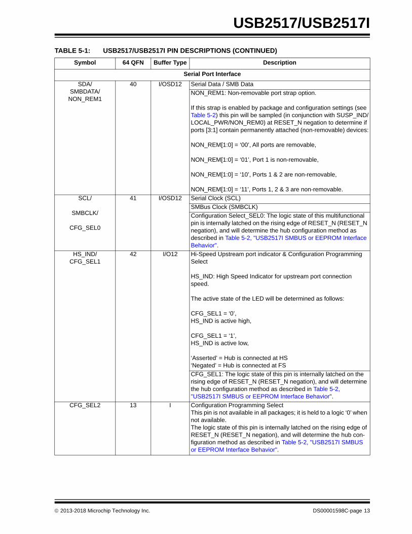
USB2517/USB2517I
Serial Port Interface
SDA/SMBDATA/
NON_REM1
40 I/OSD12 Serial Data / SMB Data
NON_REM1: Non-removable port strap option.
If this strap is enabled by package and configuration settings (see Table 5-2) this pin will be sampled (in conjunction with SUSP_IND/LOCAL_PWR/NON_REM0) at RESET_N negation to determine if ports [3:1] contain permanently attached (non-removable) devices:
NON_REM[1:0] = ‘00’, All ports are removable,
NON_REM[1:0] = ‘01’, Port 1 is non-removable,
NON_REM[1:0] = ‘10’, Ports 1 & 2 are non-removable,
NON_REM[1:0] = ‘11’, Ports 1, 2 & 3 are non-removable.
SCL/
SMBCLK/
CFG_SEL0
41 I/OSD12 Serial Clock (SCL)
SMBus Clock (SMBCLK)
Configuration Select_SEL0: The logic state of this multifunctional pin is internally latched on the rising edge of RESET_N (RESET_N negation), and will determine the hub configuration method as described in Table 5-2, "USB2517I SMBUS or EEPROM Interface Behavior".
HS_IND/CFG_SEL1
42 I/O12 Hi-Speed Upstream port indicator & Configuration Programming Select
HS_IND: High Speed Indicator for upstream port connection speed.
The active state of the LED will be determined as follows:
CFG_SEL1 = ‘0’,HS_IND is active high,
CFG_SEL1 = ‘1’,HS_IND is active low,
‘Asserted’ = Hub is connected at HS‘Negated’ = Hub is connected at FS
CFG_SEL1: The logic state of this pin is internally latched on the rising edge of RESET_N (RESET_N negation), and will determine the hub configuration method as described in Table 5-2, "USB2517I SMBUS or EEPROM Interface Behavior".
CFG_SEL2 13 I Configuration Programming SelectThis pin is not available in all packages; it is held to a logic ‘0’ when not available.The logic state of this pin is internally latched on the rising edge of RESET_N (RESET_N negation), and will determine the hub con-figuration method as described in Table 5-2, "USB2517I SMBUS or EEPROM Interface Behavior".
TABLE 5-1: USB2517/USB2517I PIN DESCRIPTIONS (CONTINUED)
Symbol 64 QFN Buffer Type Description
2013-2018 Microchip Technology Inc. DS00001598C-page 13
USB2517/USB2517I
MISC
XTAL1/CLKIN
61 ICLKx Crystal Input/External Clock Input
24MHz crystal or external clock input.This pin connects to either one terminal of the crystal or to an external 24MHz clock when a crystal is not used.
XTAL2 60 OCLKx Crystal Output
24MHz CrystalThis is the other terminal of the crystal. It can be treated as a no connect when an external clock source is used to drive XTAL1/CLKIN. This output must not be used to drive any external circuitry other than the crystal circuit.
RESET_N 43 IS RESET Input
The system can reset the chip by driving this input low. The mini-mum active low pulse is 1s.
When the RESET_N pin is pulled to VDD33, the internal POR (Power on Reset) is enabled and no external reset circuitry is required. The internal POR holds the internal logic in reset until the power supplies are stable.
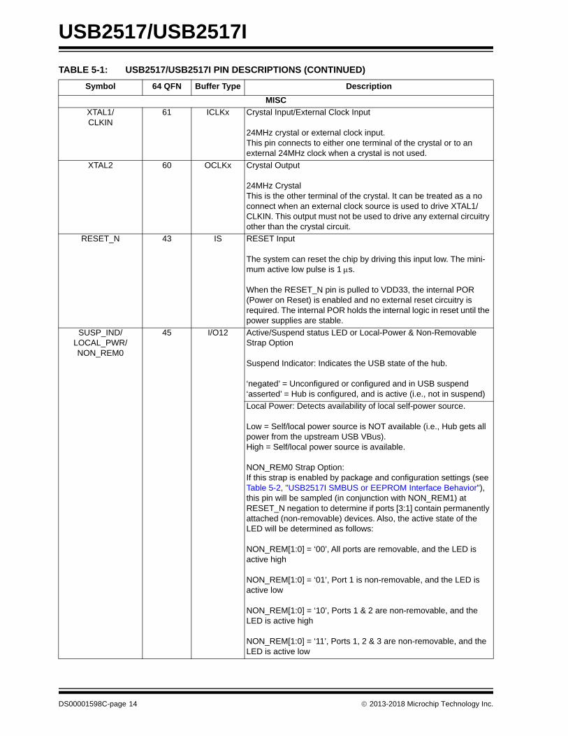
SUSP_IND/LOCAL_PWR/NON_REM0
45 I/O12 Active/Suspend status LED or Local-Power & Non-Removable Strap Option
Suspend Indicator: Indicates the USB state of the hub.
‘negated’ = Unconfigured or configured and in USB suspend‘asserted’ = Hub is configured, and is active (i.e., not in suspend)
Local Power: Detects availability of local self-power source.
Low = Self/local power source is NOT available (i.e., Hub gets all power from the upstream USB VBus).High = Self/local power source is available.
NON_REM0 Strap Option:If this strap is enabled by package and configuration settings (see Table 5-2, "USB2517I SMBUS or EEPROM Interface Behavior"), this pin will be sampled (in conjunction with NON_REM1) at RESET_N negation to determine if ports [3:1] contain permanently attached (non-removable) devices. Also, the active state of the LED will be determined as follows:
NON_REM[1:0] = ‘00’, All ports are removable, and the LED is active high
NON_REM[1:0] = ‘01’, Port 1 is non-removable, and the LED is active low
NON_REM[1:0] = ‘10’, Ports 1 & 2 are non-removable, and the LED is active high
NON_REM[1:0] = ‘11’, Ports 1, 2 & 3 are non-removable, and the LED is active low
TABLE 5-1: USB2517/USB2517I PIN DESCRIPTIONS (CONTINUED)
Symbol 64 QFN Buffer Type Description
DS00001598C-page 14 2013-2018 Microchip Technology Inc.
USB2517/USB2517I
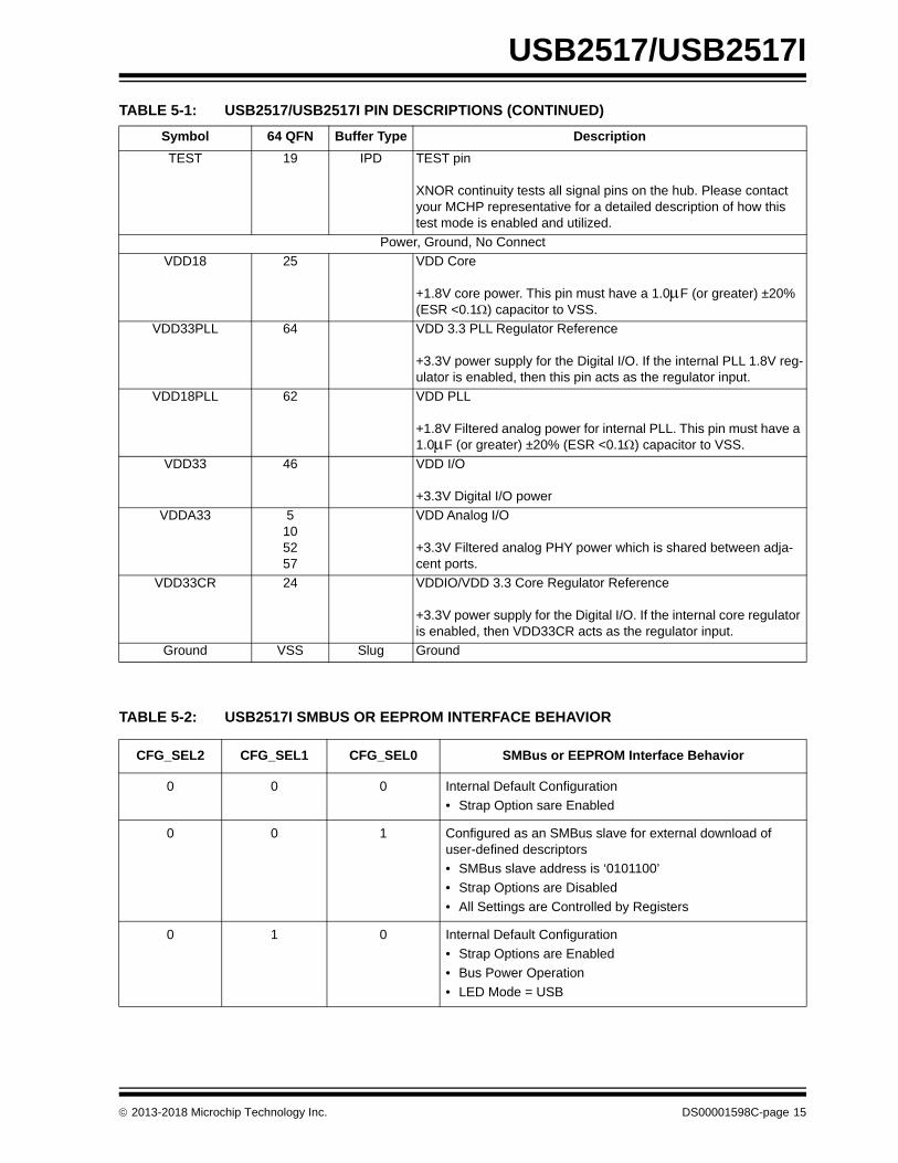
TEST 19 IPD TEST pin
XNOR continuity tests all signal pins on the hub. Please contact your MCHP representative for a detailed description of how this test mode is enabled and utilized.
Power, Ground, No Connect
VDD18 25 VDD Core
+1.8V core power. This pin must have a 1.0F (or greater) ±20% (ESR <0.1) capacitor to VSS.
VDD33PLL 64 VDD 3.3 PLL Regulator Reference
+3.3V power supply for the Digital I/O. If the internal PLL 1.8V reg-ulator is enabled, then this pin acts as the regulator input.
VDD18PLL 62 VDD PLL
+1.8V Filtered analog power for internal PLL. This pin must have a 1.0F (or greater) ±20% (ESR <0.1) capacitor to VSS.
VDD33 46 VDD I/O
+3.3V Digital I/O power
VDDA33 5105257
VDD Analog I/O
+3.3V Filtered analog PHY power which is shared between adja-cent ports.
VDD33CR 24 VDDIO/VDD 3.3 Core Regulator Reference
+3.3V power supply for the Digital I/O. If the internal core regulator is enabled, then VDD33CR acts as the regulator input.
Ground VSS Slug Ground
TABLE 5-2: USB2517I SMBUS OR EEPROM INTERFACE BEHAVIOR
CFG_SEL2 CFG_SEL1 CFG_SEL0 SMBus or EEPROM Interface Behavior
0 0 0 Internal Default Configuration
• Strap Option sare Enabled
0 0 1 Configured as an SMBus slave for external download of user-defined descriptors
• SMBus slave address is ‘0101100’
• Strap Options are Disabled
• All Settings are Controlled by Registers
0 1 0 Internal Default Configuration
• Strap Options are Enabled
• Bus Power Operation
• LED Mode = USB
TABLE 5-1: USB2517/USB2517I PIN DESCRIPTIONS (CONTINUED)
Symbol 64 QFN Buffer Type Description
2013-2018 Microchip Technology Inc. DS00001598C-page 15
USB2517/USB2517I
5.2 Buffer Type Descriptions
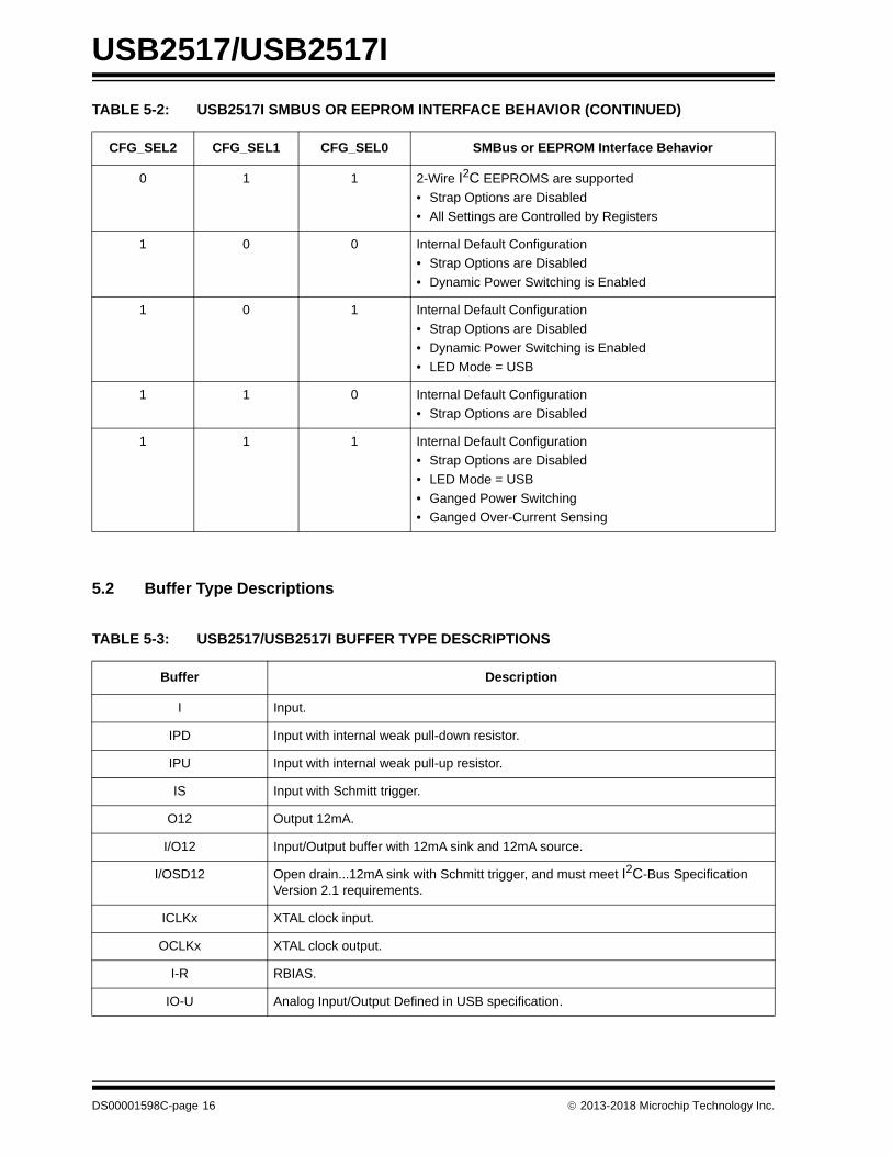
0 1 1 2-Wire I2C EEPROMS are supported
• Strap Options are Disabled
• All Settings are Controlled by Registers
1 0 0 Internal Default Configuration
• Strap Options are Disabled
• Dynamic Power Switching is Enabled
1 0 1 Internal Default Configuration
• Strap Options are Disabled
• Dynamic Power Switching is Enabled
• LED Mode = USB
1 1 0 Internal Default Configuration
• Strap Options are Disabled
1 1 1 Internal Default Configuration
• Strap Options are Disabled
• LED Mode = USB
• Ganged Power Switching
• Ganged Over-Current Sensing
TABLE 5-3: USB2517/USB2517I BUFFER TYPE DESCRIPTIONS
Buffer Description
I Input.
IPD Input with internal weak pull-down resistor.
IPU Input with internal weak pull-up resistor.
IS Input with Schmitt trigger.
O12 Output 12mA.
I/O12 Input/Output buffer with 12mA sink and 12mA source.
I/OSD12 Open drain...12mA sink with Schmitt trigger, and must meet I2C-Bus Specification Version 2.1 requirements.
ICLKx XTAL clock input.
OCLKx XTAL clock output.
I-R RBIAS.
IO-U Analog Input/Output Defined in USB specification.
TABLE 5-2: USB2517I SMBUS OR EEPROM INTERFACE BEHAVIOR (CONTINUED)
CFG_SEL2 CFG_SEL1 CFG_SEL0 SMBus or EEPROM Interface Behavior
DS00001598C-page 16 2013-2018 Microchip Technology Inc.
USB2517/USB2517I
6.0 LED USAGE DESCRIPTION
6.1 LED Functionality
The hub supports 2 different (mutually exclusive) LED modes. The USB Mode provides 14 LED’s that conform to theUSB 2.0 specification functional requirements for Green and Amber LED’s. The LED Mode “Speed indicator” providesthe downstream device connection speed.
6.1.1 USB MODE 14-WIRE
The LED_A[7:1]_N pins are used to provide Green LED support as defined in the USB 2.0 specification. TheLED_B[7:1]_N pins are used to provide Amber LED support as defined in the USB 2.0 specification. The USB Specifi-cation defines the LED’s as port status indicators for the downstream ports. Please note that no indication of port speedis possible in this mode. The pins are utilized as follows:
• LED_A1_N = Port 1 green LED
• LED_A2_N = Port 2 green LED
• LED_A3_N = Port 3 green LED
• LED_A4_N = Port 4 green LED
• LED_A5_N = Port 5 green LED
• LED_A6_N = Port 6 green LED
• LED_A7_N = Port 7 green LED
• LED_B1_N = Port 1 amber LED
• LED_B2_N = Port 2 amber LED
• LED_B3_N = Port 3 amber LED
• LED_B4_N = Port 4 amber LED
• LED_B5_N = Port 5 amber LED
• LED_B6_N = Port 6 amber LED
• LED_B7_N = Port 7 amber LED
6.1.2 LED MODE SPEED INDICATION
The LED_A[7:1]_N pins are used to provide connection status as well as port speed by using dual color LED's. Thisscheme requires that the LED's be in the same package, and that a third color is produced so that the user perceivesboth LED's as being driven "simultaneously".
The LED_A[7:1] pins used in this mode are connected to 7 dual color LED’s (each LED pair in a single package). Thesepins indicate the USB speed of each attached downstream device.
Each dual color LED provides two separate colors (commonly Green and Red). If each of these separate colors arepulsed on and off at a rapid rate, a user will see a third color (in this example, Orange). Using this method, 4 different"color" states are possible (Green, Red, Orange, and Off).
2013-2018 Microchip Technology Inc. DS00001598C-page 17
USB2517/USB2517I
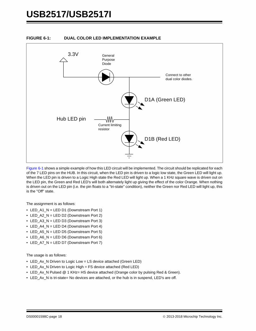
Figure 6-1 shows a simple example of how this LED circuit will be implemented. The circuit should be replicated for eachof the 7 LED pins on the HUB. In this circuit, when the LED pin is driven to a logic low state, the Green LED will light up.When the LED pin is driven to a Logic High state the Red LED will light up. When a 1 KHz square wave is driven out onthe LED pin, the Green and Red LED's will both alternately light up giving the effect of the color Orange. When nothingis driven out on the LED pin (i.e. the pin floats to a "tri-state" condition), neither the Green nor Red LED will light up, thisis the "Off" state.
The assignment is as follows:
• LED_A1_N = LED D1 (Downstream Port 1)
• LED_A2_N = LED D2 (Downstream Port 2)
• LED_A3_N = LED D3 (Downstream Port 3)
• LED_A4_N = LED D4 (Downstream Port 4)
• LED_A5_N = LED D5 (Downstream Port 5)
• LED_A6_N = LED D6 (Downstream Port 6)
• LED_A7_N = LED D7 (Downstream Port 7)
The usage is as follows:
• LED_Ax_N Driven to Logic Low = LS device attached (Green LED)
• LED_Ax_N Driven to Logic High = FS device attached (Red LED)
• LED_Ax_N Pulsed @ 1 KHz= HS device attached (Orange color by pulsing Red & Green).
• LED_Ax_N is tri-state= No devices are attached, or the hub is in suspend, LED's are off.
FIGURE 6-1: DUAL COLOR LED IMPLEMENTATION EXAMPLE
Hub LED pin
D1A (Green LED)
D1B (Red LED)
3.3V GeneralPurposeDiode
Current limiting resistor
Connect to otherdual color diodes.
DS00001598C-page 18 2013-2018 Microchip Technology Inc.
USB2517/USB2517I
7.0 CONFIGURATION OPTIONS
7.1 7-Port Hub
The USB 2.0 7-Port Hub is fully compliant to the Universal Serial Bus Specification Revision 2.0 from April 27, 2000 (12/7/2000 and 5/28/2002 Errata). Please reference Chapter 11 (Hub Specification) for general details regarding Hub oper-ation and functionality.
For performance reasons, the 7-Port Hub provides 1 Transaction Translator (TT) per port (defined as Multi-TT configu-ration), divided into 4 non-periodic buffers per TT.
7.1.1 HUB CONFIGURATION OPTIONS
The MCHP Hub supports a large number of features (some are mutually exclusive), and must be configured in order tocorrectly function when attached to a USB host controller. There are three principal ways to configure the Hub: SMBus,EEPROM, or by internal default settings (with or without pin strapping option overrides). In all cases, the configurationmethod will be determined by the CFG_SEL2, CFG_SEL1 and CFG_SEL0 pins immediately after RESET_N negation.
7.1.1.1 Power Switching Polarity
7.1.2 VBUS DETECT
According to Section 7.2.1 of the USB 2.0 Specification, a downstream port can never provide power to its D+ or D- pullup resistors unless the upstream port’s VBUS is in the asserted (powered) state. The VBUS_DET pin on the Hub mon-itors the state of the upstream VBUS signal and will not pull up the D+ resistor if VBUS is not active. If VBUS goes froman active to an inactive state (not powered), the Hub will remove power from the D+ pull up resistor within 10 seconds.
7.2 EEPROM Interface
The MCHP Hub can be configured via a 2-wire (I2C) EEPROM (256x8). (Please see Table 5-2, "USB2517I SMBUS orEEPROM Interface Behavior" for specific details on how to enable configuration via an I2C EEPROM).
The internal state machine will (when configured for EEPROM support) read the external EEPROM for configurationdata. The Hub will then “attach” to the upstream USB host.
Please see Internal Register Set (Common to EEPROM and SMBus) for a list of data fields available.
7.2.1 INTERNAL REGISTER SET (COMMON TO EEPROM AND SMBUS)
Note: The hub will support active high power controllers only!
Note: The Hub does not have the capacity to write, or “Program,” an external EEPROM. The Hub only has thecapability to read external EEPROMs. The external EEPROM will be read (even if it is blank or non-popu-lated), and the Hub will be “configured” with the values that are read.
TABLE 7-1: INTERNAL DEFAULT, EEPROM AND SMBUS REGISTER MEMORY MAP
Reg Addr R/W Register Name AbbrInternal
Default ROM
SMBus and EEPROM POR
Values
00h R/W VID LSB VIDL 24h 0x00
01h R/W VID MSB VIDM 04h 0x00
02h R/W PID LSB PIDL 17h 0x00
03h R/W PID MSB PIDM 25h 0x00
04h R/W DID LSB DIDL 00h 0x00
05h R/W DID MSB DIDM 00h 0x00
2013-2018 Microchip Technology Inc. DS00001598C-page 19
USB2517/USB2517I
06h R/W Config Data Byte 1 CFG1 9Bh 0x00
07h R/W Config Data Byte 2 CFG2 20h 0x00
08h R/W Config Data Byte 3 CFG3 00h 0x00
09h R/W Non-Removable Devices NRD 00h 0x00
0Ah R/W Port Disable (Self) PDS 00h 0x00
0Bh R/W Port Disable (Bus) PDB 00h 0x00
0Ch R/W Max Power (Self) MAXPS 01h 0x00
0Dh R/W Max Power (Bus) MAXPB 32h 0x00
0Eh R/W Hub Controller Max Current (Self)
HCMCS 01h 0x00
0Fh R/W Hub Controller Max Current (Bus)
HCMCB 32h 0x00
10h R/W Power-on Time PWRT 32h 0x00
11h R/W LANG_ID_H LANGIDH 00h 0x00
12h R/W LANG_ID_L LANGIDL 00h 0x00
13h R/W MFR_STR_LEN MFRSL 00h 0x00
14h R/W PRD_STR_LEN PRDSL 00h 0x00
15h R/W SER_STR_LEN SERSL 00h 0x00
16h-53h R/W MFR_STR MANSTR 00h 0x00
54h-91h R/W PROD_STR PRDSTR 00h 0x00
92h-Cfh R/W SER_STR SERSTR 00h 0x00
D0h-F5h R/W Reserved N/A 00h 0x00
F6h R/W Boost_Up BOOSTUP 00h 0x00
F7h R/W Boost_7:5 BOOST75 00h 0x00
F8h R/W Boost_4:0 BOOST40 00h 0x00
F9h R/W Reserved N/A 00h 0x00
FAh R/W Port Swap PRTSP 00h 0x00
FBh R/W Port Remap 12 PRTR12 00h 0x00
FCh R/W Port Remap 34 PRTR34 00h 0x00
FDh R/W Port Remap 56 PRTR56 00h 0x00
TABLE 7-1: INTERNAL DEFAULT, EEPROM AND SMBUS REGISTER MEMORY MAP
Reg Addr R/W Register Name AbbrInternal
Default ROM
SMBus and EEPROM POR
Values
DS00001598C-page 20 2013-2018 Microchip Technology Inc.
USB2517/USB2517I
7.2.1.1 Register 00h: Vendor ID (LSB)
7.2.1.2 Register 01h: Vendor ID (MSB)
7.2.1.3 Register 02h: Product ID (LSB)
FEh R/W Port Remap 7 PRTR7 00h 0x00
FFh R/W Status/Command
Note: SMBus registeronly
STCD 00h 0x00
Bit Number
Bit Name Description
7:0 VID_LSB Least Significant Byte of the Vendor ID. This is a 16-bit value that uniquely identifies the Vendor of the user device (assigned by USB-Interface Forum). This field is set by the OEM using either the SMBus or EEPROM interface options.
Bit Number
Bit Name Description
7:0 VID_MSB Most Significant Byte of the Vendor ID. This is a 16-bit value that uniquely identifies the Vendor of the user device (assigned by USB-Interface Forum). This field is set by the OEM using either the SMBus or EEPROM interface options.
Bit Number
Bit Name Description
7:0 PID_LSB Least Significant Byte of the Product ID. This is a 16-bit value that the Vendor can assign that uniquely identifies this particular product (assigned by OEM). This field is set by the OEM using either the SMBus or EEPROM interface options.
TABLE 7-1: INTERNAL DEFAULT, EEPROM AND SMBUS REGISTER MEMORY MAP
Reg Addr R/W Register Name AbbrInternal
Default ROM
SMBus and EEPROM POR
Values
2013-2018 Microchip Technology Inc. DS00001598C-page 21
USB2517/USB2517I
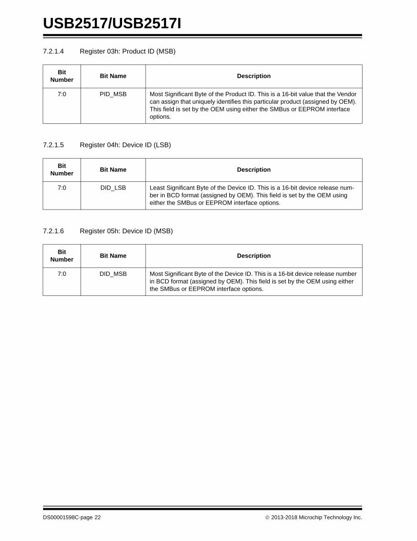
7.2.1.4 Register 03h: Product ID (MSB)
7.2.1.5 Register 04h: Device ID (LSB)
7.2.1.6 Register 05h: Device ID (MSB)
Bit Number
Bit Name Description
7:0 PID_MSB Most Significant Byte of the Product ID. This is a 16-bit value that the Vendor can assign that uniquely identifies this particular product (assigned by OEM). This field is set by the OEM using either the SMBus or EEPROM interface options.
Bit Number
Bit Name Description
7:0 DID_LSB Least Significant Byte of the Device ID. This is a 16-bit device release num-ber in BCD format (assigned by OEM). This field is set by the OEM using either the SMBus or EEPROM interface options.
Bit Number
Bit Name Description
7:0 DID_MSB Most Significant Byte of the Device ID. This is a 16-bit device release number in BCD format (assigned by OEM). This field is set by the OEM using either the SMBus or EEPROM interface options.
DS00001598C-page 22 2013-2018 Microchip Technology Inc.

USB2517/USB2517I
7.2.1.7 Register 06h: CONFIG_BYTE_1
Bit Number
Bit Name Description
7 SELF_BUS_PWR Self or Bus Power: Selects between Self- and Bus-Powered operation.
The Hub is either Self-Powered (draws less than 2mA of upstream bus power) or Bus-Powered (limited to a 100mA maximum of upstream power prior to being configured by the host controller). When configured as a Bus-Powered device, the MCHP Hub consumes less than 100mA of current prior to being configured. After configuration, the Bus-Powered MCHP Hub (along with all associated hub circuitry, any embedded devices if part of a compound device, and 100mA per externally available downstream port) must consume no more than 500mA of upstream VBUS current. The current consumption is system dependent, and the OEM must ensure that the USB 2.0 specifications are not violated.When configured as a Self-Powered device, <1mA of upstream VBUS current is consumed and all ports are available, with each port being capable of sourcing 500mA of current.This field is set by the OEM using either the SMBus or EEPROM interface options. Please see the description under Dynamic Power for the self/bus power func-tionality when dynamic power switching is enabled.
0 = Bus-Powered operation1 = Self-Powered operation
Note: If Dynamic Power Switching is enabled, this bit is ignored and theLOCAL_PWR pin is used to determine if the hub is operating fromself or bus power.
6 Reserved Reserved
5 HS_DISABLE High Speed Disable: Disables the capability to attach as either a High/Full-speed device, and forces attachment as Full-speed only (i.e. no Hi-Speed support).
0 = High-/Full-Speed1 = Full-Speed-Only (Hi-Speed disabled!)
4 MTT_ENABLE Multi-TT enable: Enables one transaction translator per port operation.
Selects between a mode where only one transaction translator is available for all ports (Single-TT), or each port gets a dedicated transaction translator (Multi-TT) {Note: The host may force single-TT mode only}.
0 = single TT for all ports1 = one TT per port (multiple TT’s supported)
3 EOP_DISABLE EOP Disable: Disables EOP generation of EOF1 when in Full-Speed mode.During FS operation only, this permits the Hub to send EOP if no downstream traffic is detected at EOF1. See Section 11.3.1 of the USB 2.0 Specification for additional details. Note: generation of an EOP at the EOF1 point may pre-vent a Host controller (operating in FS mode) from placing the USB bus in suspend.
0 = EOP generation is normal1 = EOP generation is disabled
2013-2018 Microchip Technology Inc. DS00001598C-page 23
USB2517/USB2517I
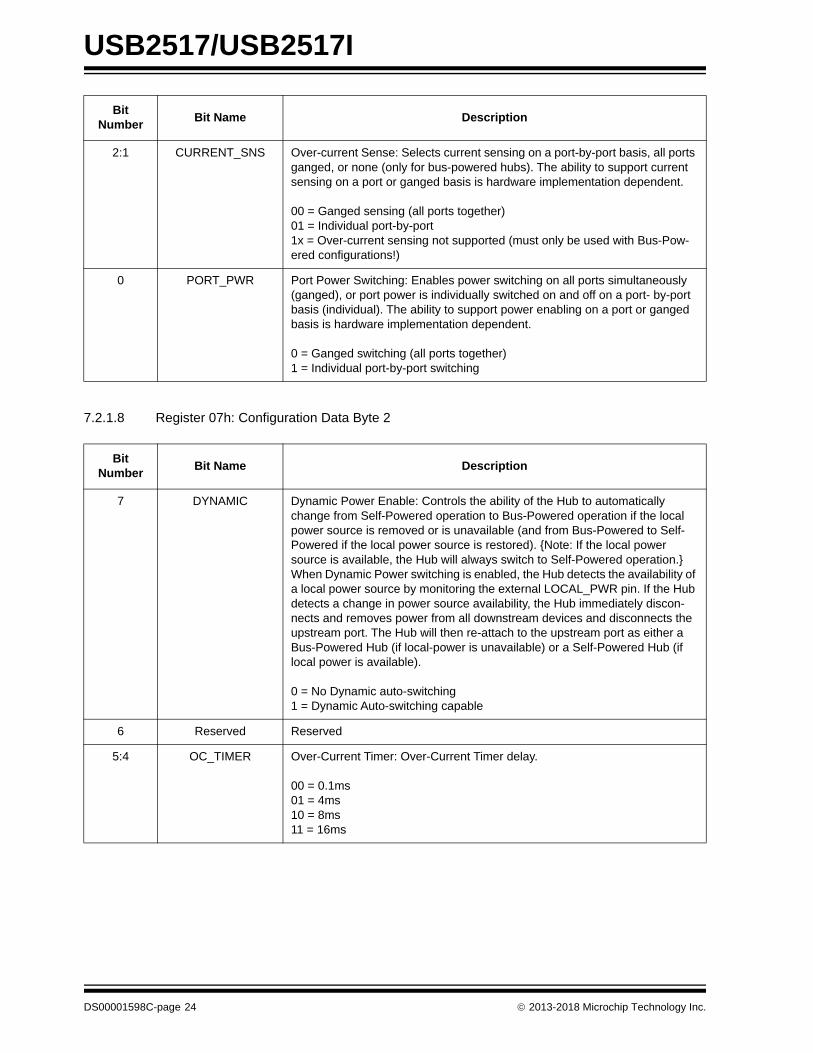
7.2.1.8 Register 07h: Configuration Data Byte 2
2:1 CURRENT_SNS Over-current Sense: Selects current sensing on a port-by-port basis, all ports ganged, or none (only for bus-powered hubs). The ability to support current sensing on a port or ganged basis is hardware implementation dependent.
00 = Ganged sensing (all ports together)01 = Individual port-by-port1x = Over-current sensing not supported (must only be used with Bus-Pow-ered configurations!)
0 PORT_PWR Port Power Switching: Enables power switching on all ports simultaneously (ganged), or port power is individually switched on and off on a port- by-port basis (individual). The ability to support power enabling on a port or ganged basis is hardware implementation dependent.
0 = Ganged switching (all ports together)1 = Individual port-by-port switching
Bit Number
Bit Name Description
7 DYNAMIC Dynamic Power Enable: Controls the ability of the Hub to automatically change from Self-Powered operation to Bus-Powered operation if the local power source is removed or is unavailable (and from Bus-Powered to Self-Powered if the local power source is restored). {Note: If the local power source is available, the Hub will always switch to Self-Powered operation.}When Dynamic Power switching is enabled, the Hub detects the availability of a local power source by monitoring the external LOCAL_PWR pin. If the Hub detects a change in power source availability, the Hub immediately discon-nects and removes power from all downstream devices and disconnects the upstream port. The Hub will then re-attach to the upstream port as either a Bus-Powered Hub (if local-power is unavailable) or a Self-Powered Hub (if local power is available).
0 = No Dynamic auto-switching1 = Dynamic Auto-switching capable
6 Reserved Reserved
5:4 OC_TIMER Over-Current Timer: Over-Current Timer delay.
00 = 0.1ms01 = 4ms10 = 8ms11 = 16ms
Bit Number
Bit Name Description
DS00001598C-page 24 2013-2018 Microchip Technology Inc.
USB2517/USB2517I
7.2.1.9 Register 08h: Configuration Data Byte 3
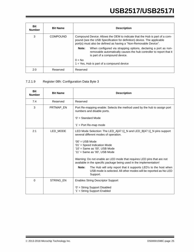
3 COMPOUND Compound Device: Allows the OEM to indicate that the Hub is part of a com-pound (see the USB Specification for definition) device. The applicable port(s) must also be defined as having a "Non-Removable Device".
Note: When configured via strapping options, declaring a port as non-removable automatically causes the hub controller to report that itis part of a compound device.
0 = No1 = Yes, Hub is part of a compound device
2:0 Reserved Reserved
Bit Number
Bit Name Description
7:4 Reserved Reserved
3 PRTMAP_EN Port Re-mapping enable: Selects the method used by the hub to assign port numbers and disable ports.
‘0’ = Standard Mode
‘1’ = Port Re-map mode
2:1 LED_MODE LED Mode Selection: The LED_A[47:1]_N and LED_B[47:1]_N pins support several different modes of operation.
‘00’ = USB Mode‘01’ = Speed Indication Mode‘10’ = Same as ‘00’, USB Mode‘11’ = Same as ‘00’, USB Mode
Warning: Do not enable an LED mode that requires LED pins that are not available in the specific package being used in the implementation!
Note: The Hub will only report that it supports LED's to the host whenUSB mode is selected. All other modes will be reported as No LEDSupport.
0 STRING_EN Enables String Descriptor Support
‘0’ = String Support Disabled‘1’ = String Support Enabled
Bit Number
Bit Name Description
2013-2018 Microchip Technology Inc. DS00001598C-page 25
USB2517/USB2517I
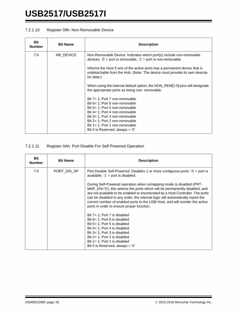
7.2.1.10 Register 09h: Non-Removable Device
7.2.1.11 Register 0Ah: Port Disable For Self Powered Operation
Bit Number
Bit Name Description
7:0 NR_DEVICE Non-Removable Device: Indicates which port(s) include non-removable devices. ‘0’ = port is removable, ‘1’ = port is non-removable.
Informs the Host if one of the active ports has a permanent device that is undetachable from the Hub. (Note: The device must provide its own descrip-tor data.)
When using the internal default option, the NON_REM[1:0] pins will designate the appropriate ports as being non- removable.
Bit 7= 1; Port 7 non-removableBit 6= 1; Port 6 non-removableBit 5= 1; Port 5 non-removableBit 4= 1; Port 4 non-removableBit 3= 1; Port 3 non-removableBit 2= 1; Port 2 non-removableBit 1= 1; Port 1 non-removableBit 0 is Reserved, always = ‘0’
Bit Number
Bit Name Description
7:0 PORT_DIS_SP Port Disable Self-Powered: Disables 1 or more contiguous ports. ‘0’ = port is available, ‘1’ = port is disabled.
During Self-Powered operation when remapping mode is disabled (PRT-MAP_EN='0'), this selects the ports which will be permanently disabled, and are not available to be enabled or enumerated by a Host Controller. The ports can be disabled in any order, the internal logic will automatically report the correct number of enabled ports to the USB Host, and will reorder the active ports in order to ensure proper function.
Bit 7= 1; Port 7 is disabledBit 6= 1; Port 6 is disabledBit 5= 1; Port 5 is disabledBit 4= 1; Port 4 is disabledBit 3= 1; Port 3 is disabledBit 2= 1; Port 2 is disabledBit 1= 1; Port 1 is disabledBit 0 is Reserved, always = ‘0’
DS00001598C-page 26 2013-2018 Microchip Technology Inc.
USB2517/USB2517I
7.2.1.12 Register 0Bh: Port Disable For Bus Powered Operation
7.2.1.13 Register 0Ch: Max Power For Self Powered Operation
Bit Number
Bit Name Description
7:0 PORT_DIS_BP Port Disable Bus-Powered: Disables 1 or more contiguous ports. ‘0’ = port is available, ‘1’ = port is disabled.
During Self-Powered operation when remapping mode is disabled (PRT-MAP_EN='0'), this selects the ports which will be permanently disabled, and are not available to be enabled or enumerated by a Host Controller. The ports can be disabled in any order, the internal logic will automatically report the correct number of enabled ports to the USB Host, and will reorder the active ports in order to ensure proper function.
When using the internal default option, the PRT_DIS_P[7:1] and PRT_DIS_M[7:1] pins will disable the appropriate ports.
Bit 7= 1; Port 7 is disabledBit 6= 1; Port 6 is disabledBit 5= 1; Port 5 is disabledBit 4= 1; Port 4 is disabledBit 3= 1; Port 3 is disabledBit 2= 1; Port 2 is disabledBit 1= 1; Port 1 is disabledBit 0 is Reserved, always = ‘0’
Bit Number
Bit Name Description
7:0 MAX_PWR_SP Max Power Self_Powered: Value in 2mA increments that the Hub consumes from an upstream port (VBUS) when operating as a self-powered hub. This value includes the hub silicon along with the combined power consumption (from VBUS) of all associated circuitry on the board. This value also includes the power consumption of a permanently attached peripheral if the hub is configured as a compound device, and the embedded peripheral reports 0mA in its descriptors.
Note: The USB 2.0 Specification does not permit this value to exceed100mA.
2013-2018 Microchip Technology Inc. DS00001598C-page 27
USB2517/USB2517I
7.2.1.14 Register 0Dh: Max Power For Bus Powered Operation
7.2.1.15 Register 0Eh: Hub Controller Max Current For Self Powered Operation
7.2.1.16 Register 0Fh: Hub Controller Max Current For Bus Powered Operation
7.2.1.17 Register 10h: Power-On Time
BIT NUMBER BIT NAME DESCRIPTION
7:0 MAX_PWR_BP Max Power Bus_Powered: Value in 2mA increments that the Hub consumes from an upstream port (VBUS) when operating as a bus-powered hub. This value includes the hub silicon along with the combined power consumption (from VBUS) of all associated circuitry on the board. This value also includes the power consumption of a permanently attached peripheral if the hub is configured as a compound device, and the embedded peripheral reports 0mA in its descriptors.
Bit Number
Bit Name Description
7:0 HC_MAX_C_SP Hub Controller Max Current Self-Powered: Value in 2mA increments that the Hub consumes from an upstream port (VBUS) when operating as a self-pow-ered hub. This value includes the hub silicon along with the combined power consumption (from VBUS) of all associated circuitry on the board. This value does NOT include the power consumption of a permanently attached periph-eral if the hub is configured as a compound device.
Note: The USB 2.0 Specification does not permit this value to exceed100mA.
A value of 50 (decimal) indicates 100mA, which is the default value.
Bit Number
Bit Name Description
7:0 HC_MAX_C_BP Hub Controller Max Current Bus-Powered: Value in 2mA increments that the Hub consumes from an upstream port (VBUS) when operating as a bus-pow-ered hub. This value will include the hub silicon along with the combined power consumption (from VBUS) of all associated circuitry on the board. This value will NOT include the power consumption of a permanently attached peripheral if the hub is configured as a compound device.
A value of 50 (decimal) would indicate 100mA, which is the default value.
Bit Number
Bit Name Description
7:0 POWER_ON_TIME Power On Time: The length of time that it takes (in 2 ms intervals) from the time the host initiated power-on sequence begins on a port until power is sta-ble on that port.
DS00001598C-page 28 2013-2018 Microchip Technology Inc.
USB2517/USB2517I
7.2.1.18 Register 11h: Language ID High
7.2.1.19 Register 12h: Language ID Low
7.2.1.20 Register 13h: Manufacturer String Length
7.2.1.21 Register 14h: Product String Length
7.2.1.22 Register 15h: Serial String Length
Bit Number
Bit Name Description
7:0 LANG_ID_H USB LANGUAGE ID (Upper 8 bits of a 16 bit ID field)
Bit Number
Bit Name Description
7:0 LANG_ID_L USB LANGUAGE ID (Lower 8 bits of a 16 bit ID field)
Bit Number
Bit Name Description
7:0 MFR_STR_LEN Manufacturer String Length
Maximum string length is 31 characters
Bit Number
Bit Name Description
7:0 PRD_STR_LEN Product String Length
Maximum string length is 31 characters
Bit Number
Bit Name Description
7:0 SER_STR_LEN Serial String Length
Maximum string length is 31 characters
2013-2018 Microchip Technology Inc. DS00001598C-page 29
USB2517/USB2517I
7.2.1.23 Register 16h-53h: Manufacturer String
7.2.1.24 Register 54h-91h: Product String
7.2.1.25 Register 92h-CFh: Serial String
Bit Number
Bit Name Description
7:0 MFR_STR Manufacturer String, UNICODE UTF-16LE per USB 2.0 Specification
Maximum string length is 31 characters (62 bytes)
Note: The string consists of individual 16 Bit UNICODE UTF-16LE char-acters. The characters will be stored starting with the LSB at theleast significant address and the MSB at the next 8-bit location(subsequent characters must be stored in sequential contiguousaddress in the same LSB, MSB manner). Some EEPROM pro-grammers may transpose the MSB and LSB, thus reversing theByte order. Please pay careful attention to the byte ordering oryour selected programming tools.
Bit Number
Bit Name Description
7:0 PRD_STR Product String, UNICODE UTF-16LE per USB 2.0 Specification
Maximum string length is 31 characters (62 bytes)
Note: The string consists of individual 16 Bit UNICODE UTF-16LE char-acters. The characters will be stored starting with the LSB at theleast significant address and the MSB at the next 8-bit location(subsequent characters must be stored in sequential contiguousaddress in the same LSB, MSB manner). Some EEPROM pro-grammers may transpose the MSB and LSB, thus reversing theByte order. Please pay careful attention to the byte ordering oryour selected programming tools.
Bit Number
Bit Name Description
7:0 SER_STR Serial String, UNICODE UTF16LE per USB 2.0 Specification
Maximum string length is 31 characters (62 bytes)
Note: The string consists of individual 16 Bit UNICODE UTF-16LE char-acters. The characters will be stored starting with the LSB at theleast significant address and the MSB at the next 8-bit location(subsequent characters must be stored in sequential contiguousaddress in the same LSB, MSB manner). Some EEPROM pro-grammers may transpose the MSB and LSB, thus reversing theByte order. Please pay careful attention to the byte ordering oryour selected programming tools.
DS00001598C-page 30 2013-2018 Microchip Technology Inc.
USB2517/USB2517I
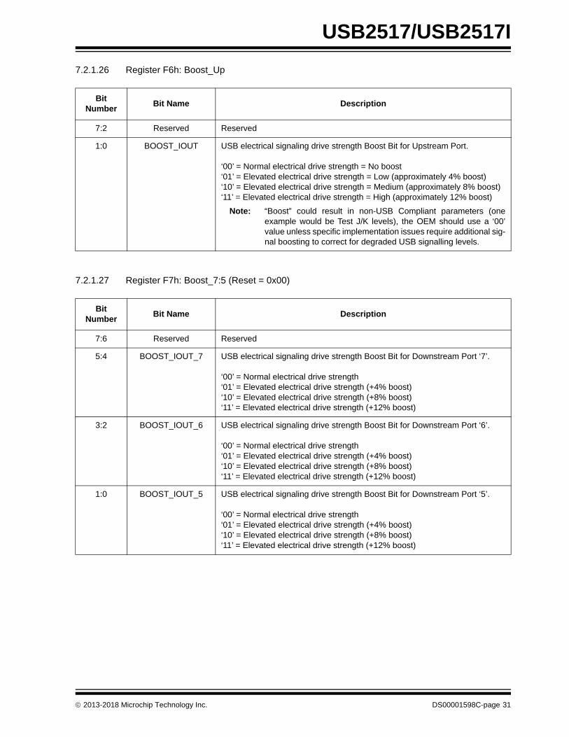
7.2.1.26 Register F6h: Boost_Up
7.2.1.27 Register F7h: Boost_7:5 (Reset = 0x00)
Bit Number
Bit Name Description
7:2 Reserved Reserved
1:0 BOOST_IOUT USB electrical signaling drive strength Boost Bit for Upstream Port.
‘00’ = Normal electrical drive strength = No boost‘01’ = Elevated electrical drive strength = Low (approximately 4% boost)‘10’ = Elevated electrical drive strength = Medium (approximately 8% boost)‘11’ = Elevated electrical drive strength = High (approximately 12% boost)
Note: “Boost” could result in non-USB Compliant parameters (oneexample would be Test J/K levels), the OEM should use a ‘00’value unless specific implementation issues require additional sig-nal boosting to correct for degraded USB signalling levels.
Bit Number
Bit Name Description
7:6 Reserved Reserved
5:4 BOOST_IOUT_7 USB electrical signaling drive strength Boost Bit for Downstream Port ‘7’.
‘00’ = Normal electrical drive strength‘01’ = Elevated electrical drive strength (+4% boost)‘10’ = Elevated electrical drive strength (+8% boost)‘11’ = Elevated electrical drive strength (+12% boost)
3:2 BOOST_IOUT_6 USB electrical signaling drive strength Boost Bit for Downstream Port ‘6’.
‘00’ = Normal electrical drive strength‘01’ = Elevated electrical drive strength (+4% boost)‘10’ = Elevated electrical drive strength (+8% boost)‘11’ = Elevated electrical drive strength (+12% boost)
1:0 BOOST_IOUT_5 USB electrical signaling drive strength Boost Bit for Downstream Port ‘5’.
‘00’ = Normal electrical drive strength‘01’ = Elevated electrical drive strength (+4% boost)‘10’ = Elevated electrical drive strength (+8% boost)‘11’ = Elevated electrical drive strength (+12% boost)
2013-2018 Microchip Technology Inc. DS00001598C-page 31
USB2517/USB2517I
7.2.1.28 Register F8h: Boost_4:0
Bit Number
Bit Name Description
7:6 BOOST_IOUT_4 USB electrical signaling drive strength Boost Bit for Downstream Port ‘4’.
‘00’ = Normal electrical drive strength = No boost‘01’ = Elevated electrical drive strength = Low (approximately 4% boost)‘10’ = Elevated electrical drive strength = Medium (approximately 8% boost)‘11’ = Elevated electrical drive strength = High (approximately 12% boost)
Note: “Boost” could result in non-USB Compliant parameters (oneexample would be Test J/K levels), the OEM should use a ‘00’value unless specific implementation issues require additional sig-nal boosting to correct for degraded USB signalling levels.
5:4 BOOST_IOUT_3 USB electrical signaling drive strength Boost Bit for Downstream Port ‘3’.
‘00’ = Normal electrical drive strength = No boost‘01’ = Elevated electrical drive strength = Low (approximately 4% boost)‘10’ = Elevated electrical drive strength = Medium (approximately 8% boost)‘11’ = Elevated electrical drive strength = High (approximately 12% boost)
Note: “Boost” could result in non-USB Compliant parameters (oneexample would be Test J/K levels), the OEM should use a ‘00’value unless specific implementation issues require additional sig-nal boosting to correct for degraded USB signalling levels.
3:2 BOOST_IOUT_2 USB electrical signaling drive strength Boost Bit for Downstream Port ‘2’.
‘00’ = Normal electrical drive strength = No boost‘01’ = Elevated electrical drive strength = Low (approximately 4% boost)‘10’ = Elevated electrical drive strength = Medium (approximately 8% boost)‘11’ = Elevated electrical drive strength = High (approximately 12% boost)
Note: “Boost” could result in non-USB Compliant parameters (oneexample would be Test J/K levels), the OEM should use a ‘00’value unless specific implementation issues require additional sig-nal boosting to correct for degraded USB signalling levels.
1:0 BOOST_IOUT_1 USB electrical signaling drive strength Boost Bit for Downstream Port ‘1’.
‘00’ = Normal electrical drive strength = No boost‘01’ = Elevated electrical drive strength = Low (approximately 4% boost)‘10’ = Elevated electrical drive strength = Medium (approximately 8% boost)‘11’ = Elevated electrical drive strength = High (approximately 12% boost)
Note: “Boost” could result in non-USB Compliant parameters (oneexample would be Test J/K levels), the OEM should use a ‘00’value unless specific implementation issues require additional sig-nal boosting to correct for degraded USB signalling levels.
DS00001598C-page 32 2013-2018 Microchip Technology Inc.
USB2517/USB2517I
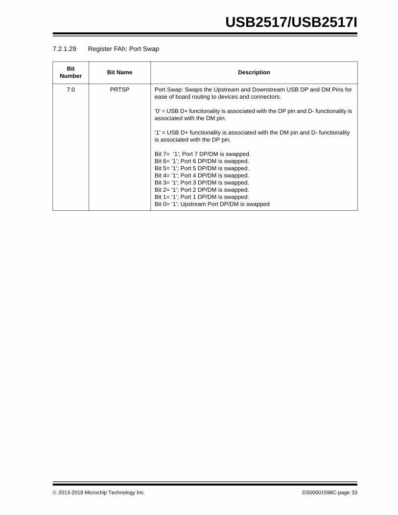
7.2.1.29 Register FAh: Port Swap
Bit Number
Bit Name Description
7:0 PRTSP Port Swap: Swaps the Upstream and Downstream USB DP and DM Pins for ease of board routing to devices and connectors.
‘0’ = USB D+ functionality is associated with the DP pin and D- functionality is associated with the DM pin.
‘1’ = USB D+ functionality is associated with the DM pin and D- functionality is associated with the DP pin.
Bit 7= ‘1’; Port 7 DP/DM is swapped.Bit 6= ’1’; Port 6 DP/DM is swapped.Bit 5= ’1’; Port 5 DP/DM is swapped.Bit 4= ‘1’; Port 4 DP/DM is swapped.Bit 3= ‘1’; Port 3 DP/DM is swapped.Bit 2= ‘1’; Port 2 DP/DM is swapped.Bit 1= ‘1’; Port 1 DP/DM is swapped.Bit 0= ‘1’; Upstream Port DP/DM is swapped
2013-2018 Microchip Technology Inc. DS00001598C-page 33

USB2517/USB2517I
7.2.1.30 Register FBh: Port Remap 12
Bit Number
Bit Name Description
7:0 PRTR12 Port remap register for ports 1 & 2
When a hub is enumerated by a USB Host Controller, the hub is only permitted to report how many ports it has; the hub is not permitted to select a numerical range or assignment. The Host Controller will number the downstream ports of the hub starting with the number '1', up to the number of ports that the hub recognizes.
The host's port number is referred to as "Logical Port Number" and the physical port on the hub is the “Physical Port Number". When remapping mode is enabled (see PRTMAP_EN in Register 08h: Configuration Data Byte 3) the hub's downstream port numbers can be remapped to different logical port numbers (assigned by the host).
Note: The OEM must ensure that Contiguous Logical Port Numbers areused, starting from #1 up to the maximum number of enabledports; this ensures that the hub's ports are numbered in accor-dance with the way a Host will communicate with the ports.
TABLE 7-2: PORT REMAP REGISTER FOR PORTS 1 & 2
Bit [7:4] ‘0000’ Physical Port 2 is Disabled
‘0001’ Physical Port 2 is mapped to Logical Port 1
‘0010’ Physical Port 2 is mapped to Logical Port 2
‘0011’ Physical Port 2 is mapped to Logical Port 3
‘0100’ Physical Port 2 is mapped to Logical Port 4
‘0101’ Physical Port 2 is mapped to Logical Port 5
‘0110’ Physical Port 2 is mapped to Logical Port 6
‘0111’ Physical Port 2 is mapped to Logical Port 7
‘1000’to
‘1111’
Reserved, will default to ‘0000’ value
Bit [3:0] ‘0000’ Physical Port 1 is Disabled
‘0001’ Physical Port 1 is mapped to Logical Port 1
‘0010’ Physical Port 1 is mapped to Logical Port 2
‘0011’ Physical Port 1 is mapped to Logical Port 3
‘0100’ Physical Port 1 is mapped to Logical Port 4
‘0101’ Physical Port 1 is mapped to Logical Port 5
‘0110’ Physical Port 1 is mapped to Logical Port 6
‘0111’ Physical Port 1 is mapped to Logical Port 7
‘1000’ to ‘1111’
Reserved, will default to ‘0000’ value
DS00001598C-page 34 2013-2018 Microchip Technology Inc.
USB2517/USB2517I
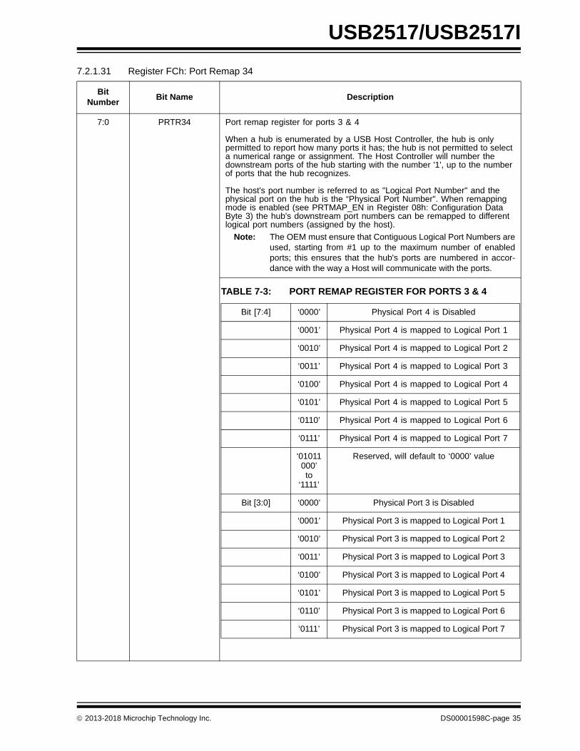
7.2.1.31 Register FCh: Port Remap 34
Bit Number
Bit Name Description
7:0 PRTR34 Port remap register for ports 3 & 4
When a hub is enumerated by a USB Host Controller, the hub is only permitted to report how many ports it has; the hub is not permitted to select a numerical range or assignment. The Host Controller will number the downstream ports of the hub starting with the number '1', up to the number of ports that the hub recognizes.
The host's port number is referred to as "Logical Port Number" and the physical port on the hub is the “Physical Port Number". When remapping mode is enabled (see PRTMAP_EN in Register 08h: Configuration Data Byte 3) the hub's downstream port numbers can be remapped to different logical port numbers (assigned by the host).
Note: The OEM must ensure that Contiguous Logical Port Numbers areused, starting from #1 up to the maximum number of enabledports; this ensures that the hub's ports are numbered in accor-dance with the way a Host will communicate with the ports.
TABLE 7-3: PORT REMAP REGISTER FOR PORTS 3 & 4
Bit [7:4] ‘0000’ Physical Port 4 is Disabled
‘0001’ Physical Port 4 is mapped to Logical Port 1
‘0010’ Physical Port 4 is mapped to Logical Port 2
‘0011’ Physical Port 4 is mapped to Logical Port 3
‘0100’ Physical Port 4 is mapped to Logical Port 4
‘0101’ Physical Port 4 is mapped to Logical Port 5
‘0110’ Physical Port 4 is mapped to Logical Port 6
‘0111’ Physical Port 4 is mapped to Logical Port 7
‘01011000’to
‘1111’
Reserved, will default to ‘0000’ value
Bit [3:0] ‘0000’ Physical Port 3 is Disabled
‘0001’ Physical Port 3 is mapped to Logical Port 1
‘0010’ Physical Port 3 is mapped to Logical Port 2
‘0011’ Physical Port 3 is mapped to Logical Port 3
‘0100’ Physical Port 3 is mapped to Logical Port 4
‘0101’ Physical Port 3 is mapped to Logical Port 5
‘0110’ Physical Port 3 is mapped to Logical Port 6
‘0111’ Physical Port 3 is mapped to Logical Port 7
2013-2018 Microchip Technology Inc. DS00001598C-page 35
USB2517/USB2517I
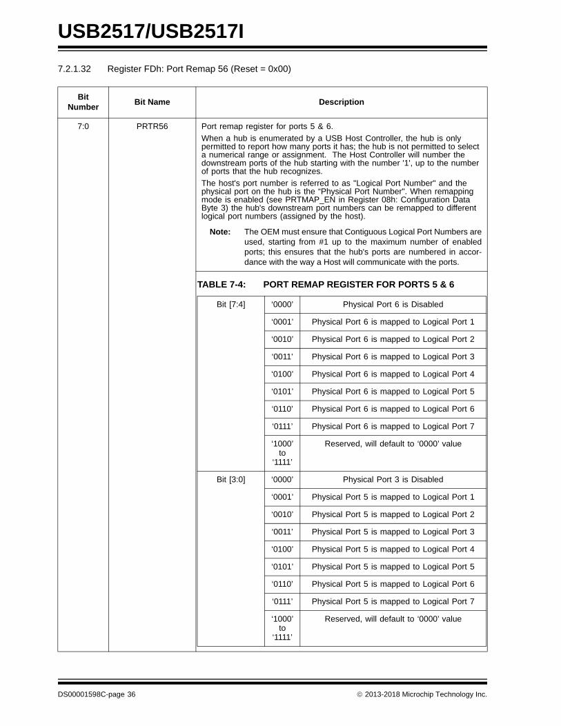
7.2.1.32 Register FDh: Port Remap 56 (Reset = 0x00)
Bit Number
Bit Name Description
7:0 PRTR56 Port remap register for ports 5 & 6.
When a hub is enumerated by a USB Host Controller, the hub is only permitted to report how many ports it has; the hub is not permitted to select a numerical range or assignment. The Host Controller will number the downstream ports of the hub starting with the number '1', up to the number of ports that the hub recognizes.
The host's port number is referred to as "Logical Port Number" and the physical port on the hub is the “Physical Port Number". When remapping mode is enabled (see PRTMAP_EN in Register 08h: Configuration Data Byte 3) the hub's downstream port numbers can be remapped to different logical port numbers (assigned by the host).
Note: The OEM must ensure that Contiguous Logical Port Numbers areused, starting from #1 up to the maximum number of enabledports; this ensures that the hub's ports are numbered in accor-dance with the way a Host will communicate with the ports.
TABLE 7-4: PORT REMAP REGISTER FOR PORTS 5 & 6
Bit [7:4] ‘0000’ Physical Port 6 is Disabled
‘0001’ Physical Port 6 is mapped to Logical Port 1
‘0010’ Physical Port 6 is mapped to Logical Port 2
‘0011’ Physical Port 6 is mapped to Logical Port 3
‘0100’ Physical Port 6 is mapped to Logical Port 4
‘0101’ Physical Port 6 is mapped to Logical Port 5
‘0110’ Physical Port 6 is mapped to Logical Port 6
‘0111’ Physical Port 6 is mapped to Logical Port 7
‘1000’to
‘1111’
Reserved, will default to ‘0000’ value
Bit [3:0] ‘0000’ Physical Port 3 is Disabled
‘0001’ Physical Port 5 is mapped to Logical Port 1
‘0010’ Physical Port 5 is mapped to Logical Port 2
‘0011’ Physical Port 5 is mapped to Logical Port 3
‘0100’ Physical Port 5 is mapped to Logical Port 4
‘0101’ Physical Port 5 is mapped to Logical Port 5
‘0110’ Physical Port 5 is mapped to Logical Port 6
‘0111’ Physical Port 5 is mapped to Logical Port 7
‘1000’to
‘1111’
Reserved, will default to ‘0000’ value
DS00001598C-page 36 2013-2018 Microchip Technology Inc.
USB2517/USB2517I
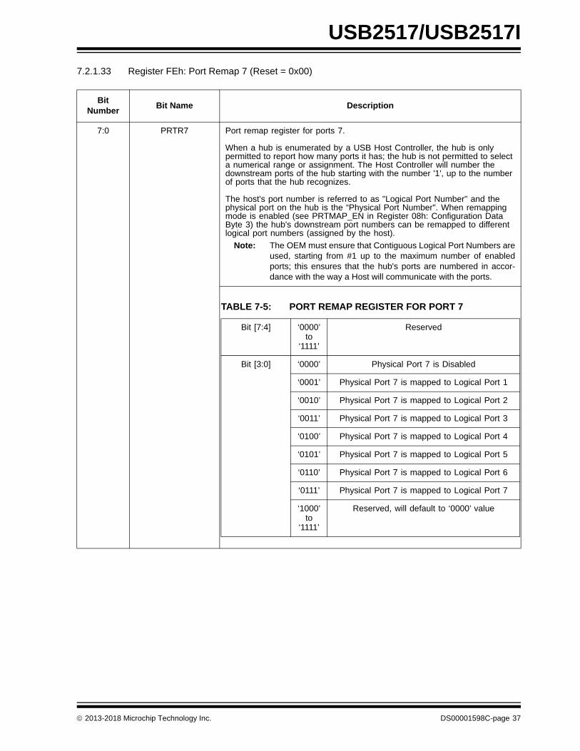
7.2.1.33 Register FEh: Port Remap 7 (Reset = 0x00)
Bit Number
Bit Name Description
7:0 PRTR7 Port remap register for ports 7.
When a hub is enumerated by a USB Host Controller, the hub is only permitted to report how many ports it has; the hub is not permitted to select a numerical range or assignment. The Host Controller will number the downstream ports of the hub starting with the number '1', up to the number of ports that the hub recognizes.
The host's port number is referred to as "Logical Port Number" and the physical port on the hub is the “Physical Port Number". When remapping mode is enabled (see PRTMAP_EN in Register 08h: Configuration Data Byte 3) the hub's downstream port numbers can be remapped to different logical port numbers (assigned by the host).
Note: The OEM must ensure that Contiguous Logical Port Numbers areused, starting from #1 up to the maximum number of enabledports; this ensures that the hub's ports are numbered in accor-dance with the way a Host will communicate with the ports.
TABLE 7-5: PORT REMAP REGISTER FOR PORT 7
Bit [7:4] ‘0000’ to
‘1111’
Reserved
Bit [3:0] ‘0000’ Physical Port 7 is Disabled
‘0001’ Physical Port 7 is mapped to Logical Port 1
‘0010’ Physical Port 7 is mapped to Logical Port 2
‘0011’ Physical Port 7 is mapped to Logical Port 3
‘0100’ Physical Port 7 is mapped to Logical Port 4
‘0101’ Physical Port 7 is mapped to Logical Port 5
‘0110’ Physical Port 7 is mapped to Logical Port 6
‘0111’ Physical Port 7 is mapped to Logical Port 7
‘1000’to
‘1111’
Reserved, will default to ‘0000’ value
2013-2018 Microchip Technology Inc. DS00001598C-page 37

USB2517/USB2517I
7.2.1.34 Register FFh: Status/Command
7.2.2 I2C EEPROM
The I2C EEPROM interface implements a subset of the I2C Master Specification (Please refer to the Philips Semicon-ductor Standard I2C-Bus Specification for details on I2C bus protocols). The Hub’s I2C EEPROM interface is designedto attach to a single “dedicated” I2C EEPROM, and conforms to the Standard-mode I2C Specification (100kbit/s transferrate and 7-bit addressing) for protocol and electrical compatibility.
The Hub acts as the master and generates the serial clock SCL, controls the bus access (determines which device actsas the transmitter and which device acts as the receiver), and generates the START and STOP conditions.
7.2.2.1 Implementation Characteristics
The Hub will only access an EEPROM using the Sequential Read Protocol.
7.2.2.2 Pull-Up Resistor
The Circuit board designer is required to place external pull-up resistors (10K recommended) on the SDA/SMBDATA& SCL/SMBCLK/CFG_SELO lines (per SMBus 1.0 Specification, and EEPROM manufacturer guidelines) to Vcc inorder to assure proper operation.
7.2.2.3 I2C EEPROM Slave Address
Slave address is 1010000.
7.2.3 IN-CIRCUIT EEPROM PROGRAMMING
The EEPROM can be programmed via ATE by pulling RESET_N low (which tri-states the Hub’s EEPROM interface andallows an external source to program the EEPROM).
Bit Number
Bit Name Description
7:3 Reserved Reserved
2 INTF_PW_DN SMBus Interface Power Down
‘0’ = Interface is active‘1’ = Interface power down after ACK has completed
1 RESET Reset the SMBus Interface and internal memory back to RESET_N assertion default settings.
‘0’ = Normal Run/Idle State‘1’ = Force a reset of registers to their default state
0 USB_ATTACH USB Attach (and write protect)
‘0’ = SMBus slave interface is active‘1’ = Hub will signal a USB attach event to an upstream device. The internal memory (address range 00h-FEh) is “write-protected” to prevent uninten-tional data corruption.
Note: Extensions to the I2C Specification are not supported.
Note: 10-bit addressing is NOT supported.
DS00001598C-page 38 2013-2018 Microchip Technology Inc.
USB2517/USB2517I
7.3 SMBus Slave Interface
Instead of loading User-Defined Descriptor data from an external EEPROM, the MCHP Hub can be configured toreceive a code load from an external processor via an SMBus interface. The SMBus interface shares the same pins asthe EEPROM interface; if CFG_SEL1 & CFG_SEL0 activates the SMBus interface, external EEPROM support is nolonger available (and the user-defined descriptor data must be downloaded via the SMBus). Due to system issues, theMCHP Hub waits indefinitely for the SMBus code load to complete and only “appears” as a newly connected device onUSB after the code load is complete.
The Hub’s SMBus implementation is a subset of the SMBus interface to the host. The device is a slave-only SMBusdevice. The implementation in the device is a subset of SMBus since it only supports two protocols.
The Write Block and Read Block protocols are the only valid SMBus protocols for the Hub. The Hub responds to otherprotocols as described in Section 7.3.2, "Invalid Protocol Response Behavior," on page 40. Reference the System Man-agement Bus Specification, Rev 1.0.
The SMBus interface is used to read and write the registers in the device. The register set is shown in Section 7.2.1,"Internal Register Set (Common to EEPROM and SMBus)," on page 19.
7.3.1 BUS PROTOCOLS
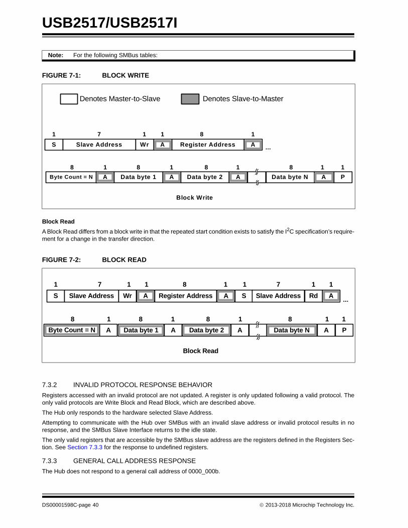
Typical Write Block and Read Block protocols are shown below. Register accesses are performed using 7-bit slaveaddressing, an 8-bit register address field, and an 8-bit data field. The shading indicates the Hub driving data on theSMBDATA line; otherwise, host data is on the SDA/SMBDATA line.
The slave address is the unique SMBus Interface Address for the Hub that identifies it on SMBus. The register addressfield is the internal address of the register to be accessed. The register data field is the data that the host is attemptingto write to the register or the contents of the register that the host is attempting to read.
7.3.1.1 Block Read/Write
The Block Write begins with a slave address and a write condition. After the command code, the host issues a bytecount which describes how many more bytes will follow in the message. If a slave had 20 bytes to send, the first bytewould be the number 20 (14h), followed by the 20 bytes of data. The byte count may not be 0. A Block Read or Write isallowed to transfer a maximum of 32 data bytes.
Note: Data bytes are transferred MSB first (msb first).
2013-2018 Microchip Technology Inc. DS00001598C-page 39
USB2517/USB2517I
Block Read
A Block Read differs from a block write in that the repeated start condition exists to satisfy the I2C specification’s require-ment for a change in the transfer direction.
7.3.2 INVALID PROTOCOL RESPONSE BEHAVIOR
Registers accessed with an invalid protocol are not updated. A register is only updated following a valid protocol. Theonly valid protocols are Write Block and Read Block, which are described above.
The Hub only responds to the hardware selected Slave Address.
Attempting to communicate with the Hub over SMBus with an invalid slave address or invalid protocol results in noresponse, and the SMBus Slave Interface returns to the idle state.
The only valid registers that are accessible by the SMBus slave address are the registers defined in the Registers Sec-tion. See Section 7.3.3 for the response to undefined registers.
7.3.3 GENERAL CALL ADDRESS RESPONSE
The Hub does not respond to a general call address of 0000_000b.
Note: For the following SMBus tables:
FIGURE 7-1: BLOCK WRITE
FIGURE 7-2: BLOCK READ
Denotes Master-to-Slave Denotes Slave-to-Master
18 1
S Slave Address Register AddressWr A
1 7 1 1 8
A
1
...
Byte Count = N A Data byte 1 A Data byte 2
8 1 1 18 8
Data byte N A P
Block Write
A
Block Read
1
SS Slave Address Register AddressWr A
1 7 1 1 8
A
1
Slave Address Rd A
7 1 1
8 1 1 18 8
P
18 1
A AAAByte Count = N Data byte 1 Data byte 2 Data byte N
...
DS00001598C-page 40 2013-2018 Microchip Technology Inc.
USB2517/USB2517I
7.3.4 SLAVE DEVICE TIME-OUT
According to the SMBus Specification, V1.0 devices in a transfer can abort the transfer in progress and release the buswhen any single clock low interval exceeds 25ms (TTIMEOUT, MIN). Devices that have detected this condition must resettheir communication and be able to receive a new START condition no later than 35ms (TTIMEOUT, MAX).
7.3.5 STRETCHING THE SCLK SIGNAL
The Hub supports stretching of the SCLK by other devices on the SMBus. The Hub does not stretch the SCLK.
7.3.6 SMBUS TIMING
The SMBus Slave Interface complies with the SMBus AC Timing Specification. See the SMBus timing in the “TimingDiagram” section.
7.3.7 BUS RESET SEQUENCE
The SMBus Slave Interface resets and returns to the idle state upon a START field followed immediately by a STOPfield.
7.3.8 SMBUS ALERT RESPONSE ADDRESS
The SMBALERT# signal is not supported by the Hub.
7.3.8.1 Undefined Registers
The registers shown in Table 7-1 are the defined registers in the Hub. Reads to undefined registers return to 00h. Writesto undefined registers have no effect and do not return an error.
7.3.8.2 Reserved Registers
Unless otherwise instructed, only a ‘0’ may be written to all reserved registers or bits.
7.4 Default Configuration Option
The MCHP Hub can be configured via its internal default configuration. (Please see Section 7.2.1, "Internal Register Set(Common to EEPROM and SMBus)" for specific details on how to enable default configuration.)
Please refer to Table 7-1 for the internal default values that are loaded when this option is selected.
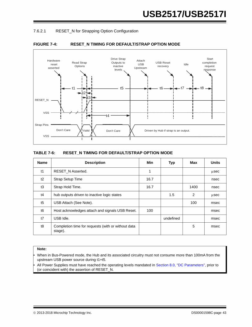
7.5 Default Strapping Options:
The USB2517/USB2517I can be configured via a combination of internal default values and pin strap options. Pleasesee Table 5-1, "USB2517/USB2517I Pin Descriptions" and Table 5-2, "USB2517I SMBUS or EEPROM InterfaceBehavior" for specific details on how to enable the default/pin-strap configuration option.
The strapping option pins only cover a limited sub-set of the configuration options. The internal default values will beused for the bits & registers that are not controlled by a strapping option pin. Please refer to Table 7-1 for the internaldefault values that are loaded when this option is selected.
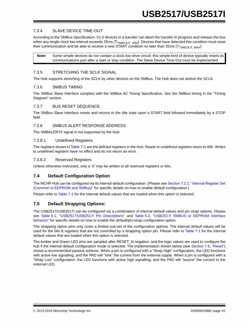
The Amber and Green LED pins are sampled after RESET_N negation, and the logic values are used to configure thehub if the internal default configuration mode is selected. The implementation shown below (see Section 7.6, "Reset")shows a recommended passive scheme. When a pin is configured with a “Strap High” configuration, the LED functionswith active low signalling, and the PAD will “sink” the current from the external supply. When a pin is configured with a“Strap Low” configuration, the LED functions with active high signalling, and the PAD will “source” the current to theexternal LED.
Note: Some simple devices do not contain a clock low drive circuit; this simple kind of device typically resets itscommunications port after a start or stop condition. The Slave Device Time-Out must be implemented.
2013-2018 Microchip Technology Inc. DS00001598C-page 41
USB2517/USB2517I
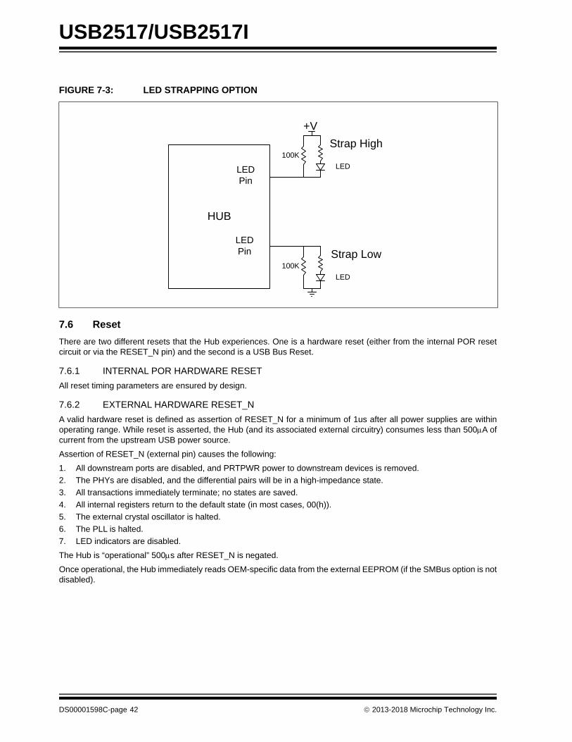
7.6 Reset
There are two different resets that the Hub experiences. One is a hardware reset (either from the internal POR resetcircuit or via the RESET_N pin) and the second is a USB Bus Reset.
7.6.1 INTERNAL POR HARDWARE RESET
All reset timing parameters are ensured by design.
7.6.2 EXTERNAL HARDWARE RESET_N
A valid hardware reset is defined as assertion of RESET_N for a minimum of 1us after all power supplies are withinoperating range. While reset is asserted, the Hub (and its associated external circuitry) consumes less than 500A ofcurrent from the upstream USB power source.
Assertion of RESET_N (external pin) causes the following:
1. All downstream ports are disabled, and PRTPWR power to downstream devices is removed.
2. The PHYs are disabled, and the differential pairs will be in a high-impedance state.
3. All transactions immediately terminate; no states are saved.
4. All internal registers return to the default state (in most cases, 00(h)).
5. The external crystal oscillator is halted.
6. The PLL is halted.
7. LED indicators are disabled.
The Hub is “operational” 500s after RESET_N is negated.
Once operational, the Hub immediately reads OEM-specific data from the external EEPROM (if the SMBus option is notdisabled).
FIGURE 7-3: LED STRAPPING OPTION
HUB
100KStrap Low
LEDPin
100KStrap High
LEDPin
+V
LED
LED
DS00001598C-page 42 2013-2018 Microchip Technology Inc.
USB2517/USB2517I
7.6.2.1 RESET_N for Strapping Option Configuration
FIGURE 7-4: RESET_N TIMING FOR DEFAULT/STRAP OPTION MODE
TABLE 7-6: RESET_N TIMING FOR DEFAULT/STRAP OPTION MODE
Name Description Min Typ Max Units
t1 RESET_N Asserted. 1 sec
t2 Strap Setup Time 16.7 nsec
t3 Strap Hold Time. 16.7 1400 nsec
t4 hub outputs driven to inactive logic states 1.5 2 sec
t5 USB Attach (See Note). 100 msec
t6 Host acknowledges attach and signals USB Reset. 100 msec
t7 USB Idle. undefined msec
t8 Completion time for requests (with or without data stage).
5 msec
Note:
• When in Bus-Powered mode, the Hub and its associated circuitry must not consume more than 100mA from the upstream USB power source during t1+t5.
• All Power Supplies must have reached the operating levels mandated in Section 8.0, "DC Parameters", prior to (or coincident with) the assertion of RESET_N.
t1
t4
t5 t6 t7 t8
Valid Don’t CareDon’t Care Driven by Hub if strap is an output.
RESET_N
VSS
Strap Pins
VSS
Hardwarereset
asserted
Read StrapOptions
Drive StrapOutputs to
inactivelevels
AttachUSB
Upstream
USB Resetrecovery
Idle
Startcompletion
requestresponse
t2t3
2013-2018 Microchip Technology Inc. DS00001598C-page 43
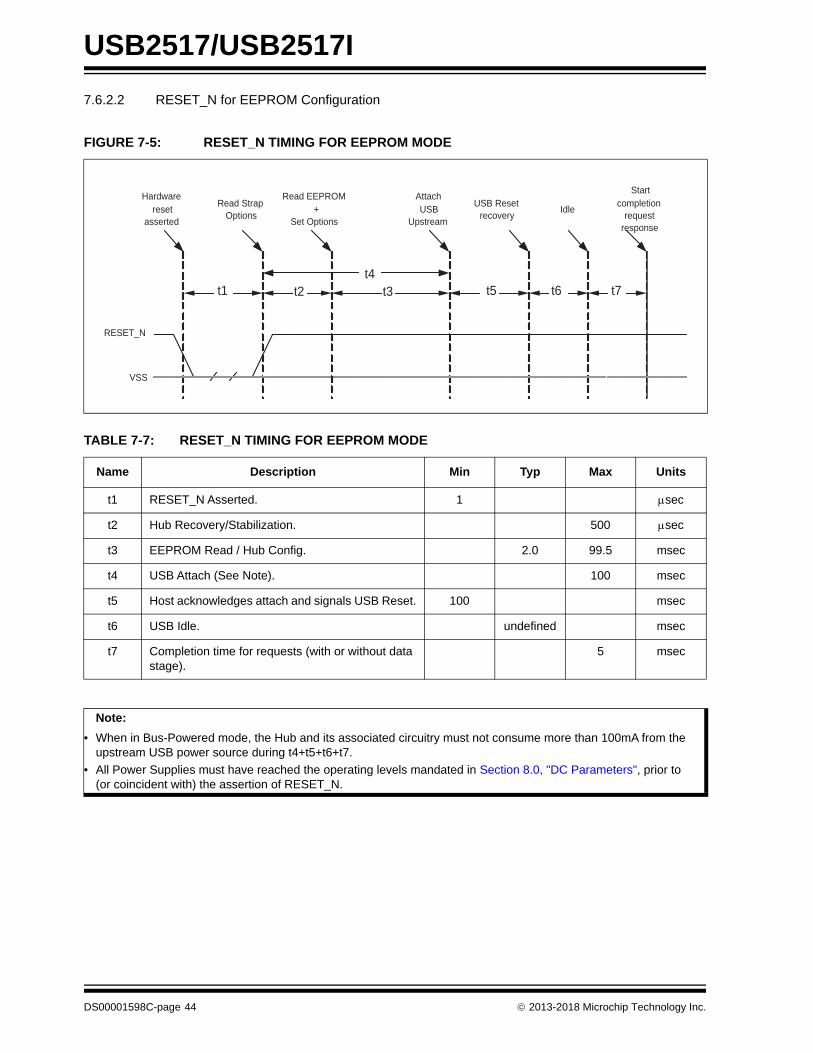
USB2517/USB2517I
7.6.2.2 RESET_N for EEPROM Configuration
FIGURE 7-5: RESET_N TIMING FOR EEPROM MODE
TABLE 7-7: RESET_N TIMING FOR EEPROM MODE
Name Description Min Typ Max Units
t1 RESET_N Asserted. 1 sec
t2 Hub Recovery/Stabilization. 500 sec
t3 EEPROM Read / Hub Config. 2.0 99.5 msec
t4 USB Attach (See Note). 100 msec
t5 Host acknowledges attach and signals USB Reset. 100 msec
t6 USB Idle. undefined msec
t7 Completion time for requests (with or without data stage).
5 msec
Note:
• When in Bus-Powered mode, the Hub and its associated circuitry must not consume more than 100mA from the upstream USB power source during t4+t5+t6+t7.
• All Power Supplies must have reached the operating levels mandated in Section 8.0, "DC Parameters", prior to (or coincident with) the assertion of RESET_N.
t1 t2t4
t5 t6 t7
RESET_N
VSS
Hardwarereset
asserted
Read StrapOptions
Read EEPROM+
Set Options
AttachUSB
Upstream
USB Resetrecovery
Idle
Startcompletion
requestresponse
t3
DS00001598C-page 44 2013-2018 Microchip Technology Inc.
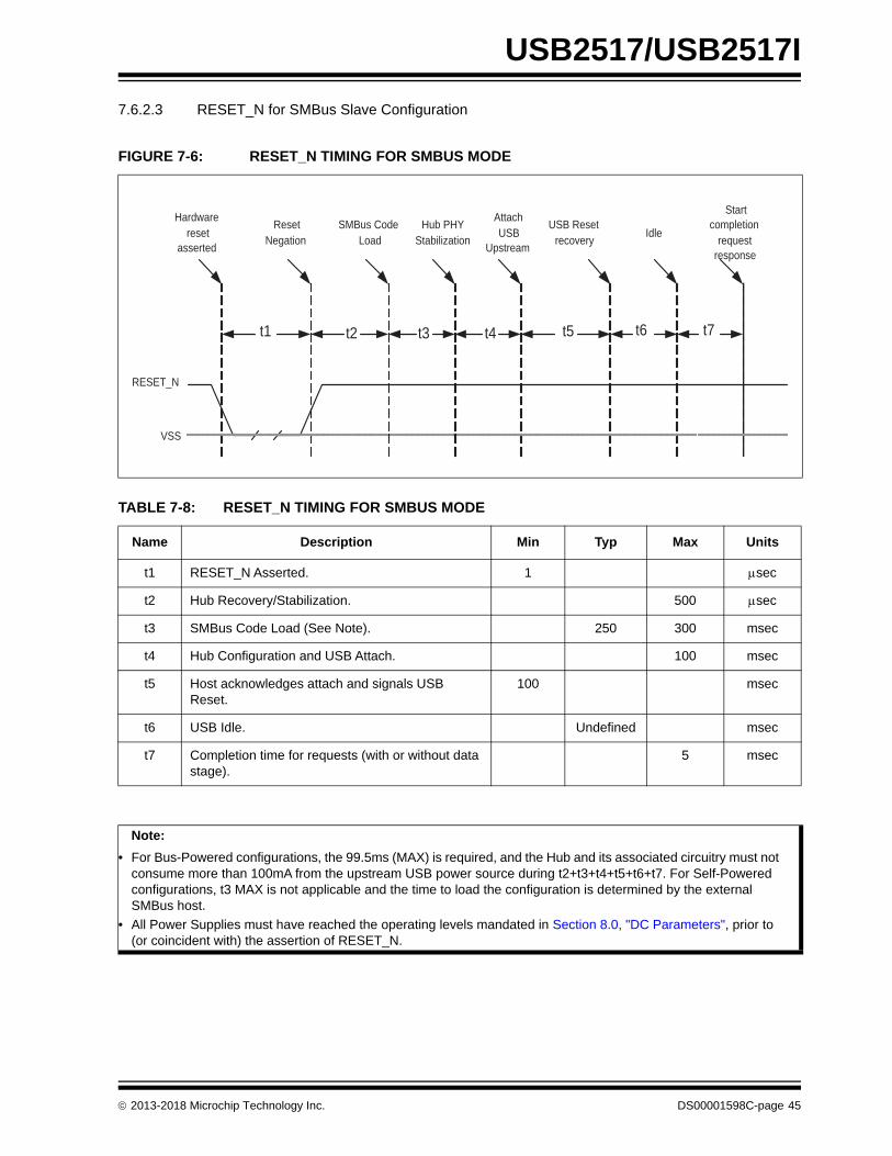
USB2517/USB2517I
7.6.2.3 RESET_N for SMBus Slave Configuration
FIGURE 7-6: RESET_N TIMING FOR SMBUS MODE
TABLE 7-8: RESET_N TIMING FOR SMBUS MODE
Name Description Min Typ Max Units
t1 RESET_N Asserted. 1 sec
t2 Hub Recovery/Stabilization. 500 sec
t3 SMBus Code Load (See Note). 250 300 msec
t4 Hub Configuration and USB Attach. 100 msec
t5 Host acknowledges attach and signals USB Reset.
100 msec
t6 USB Idle. Undefined msec
t7 Completion time for requests (with or without data stage).
5 msec
Note:
• For Bus-Powered configurations, the 99.5ms (MAX) is required, and the Hub and its associated circuitry must not consume more than 100mA from the upstream USB power source during t2+t3+t4+t5+t6+t7. For Self-Powered configurations, t3 MAX is not applicable and the time to load the configuration is determined by the external SMBus host.
• All Power Supplies must have reached the operating levels mandated in Section 8.0, "DC Parameters", prior to (or coincident with) the assertion of RESET_N.
t1 t2 t4 t5 t6 t7
RESET_N
VSS
Hardwarereset
asserted
ResetNegation
SMBus CodeLoad
AttachUSB
Upstream
USB Resetrecovery
Idle
Startcompletion
requestresponse
t3
Hub PHYStabilization
2013-2018 Microchip Technology Inc. DS00001598C-page 45

USB2517/USB2517I
7.6.3 USB BUS RESET
In response to the upstream port signaling a reset to the Hub, the Hub does the following:
1. Sets default address to 0.
2. Sets configuration to: Unconfigured.
1. Negates PRTPWR[7:1] to all downstream ports.
2. Clears all TT buffers.
3. Moves device from suspended to active (if suspended).
4. Complies with Section 11.10 of the USB 2.0 Specification for behavior after completion of the resetsequence.
The Host then configures the Hub and the Hub’s downstream port devices in accordance with the USB Specification.
Note: The Hub does not propagate the upstream USB reset to downstream devices.
DS00001598C-page 46 2013-2018 Microchip Technology Inc.
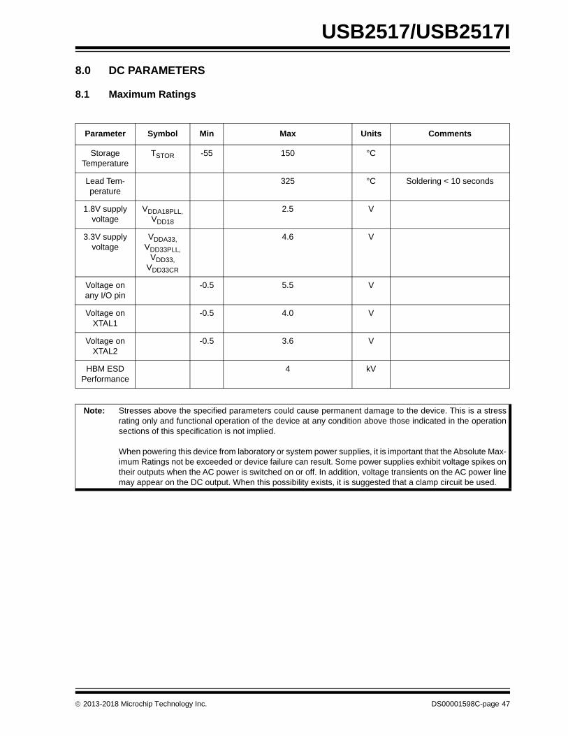
USB2517/USB2517I
8.0 DC PARAMETERS
8.1 Maximum Ratings
Parameter Symbol Min Max Units Comments
Storage Temperature
TSTOR -55 150 °C
Lead Tem-perature
325 °C Soldering < 10 seconds
1.8V supply voltage
VDDA18PLL,VDD18
2.5 V
3.3V supply voltage
VDDA33,VDD33PLL,
VDD33, VDD33CR
4.6 V
Voltage on any I/O pin
-0.5 5.5 V
Voltage on XTAL1
-0.5 4.0 V
Voltage on XTAL2
-0.5 3.6 V
HBM ESD Performance
4 kV
Note: Stresses above the specified parameters could cause permanent damage to the device. This is a stressrating only and functional operation of the device at any condition above those indicated in the operationsections of this specification is not implied.
When powering this device from laboratory or system power supplies, it is important that the Absolute Max-imum Ratings not be exceeded or device failure can result. Some power supplies exhibit voltage spikes ontheir outputs when the AC power is switched on or off. In addition, voltage transients on the AC power linemay appear on the DC output. When this possibility exists, it is suggested that a clamp circuit be used.
2013-2018 Microchip Technology Inc. DS00001598C-page 47
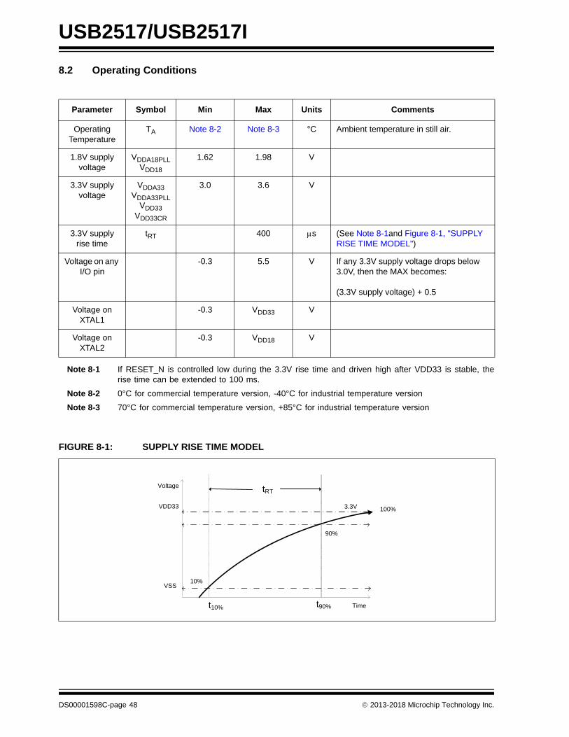
USB2517/USB2517I
8.2 Operating Conditions
Note 8-1 If RESET_N is controlled low during the 3.3V rise time and driven high after VDD33 is stable, therise time can be extended to 100 ms.
Note 8-2 0°C for commercial temperature version, -40°C for industrial temperature version
Note 8-3 70°C for commercial temperature version, +85°C for industrial temperature version
Parameter Symbol Min Max Units Comments
Operating Temperature
TA Note 8-2 Note 8-3 °C Ambient temperature in still air.
1.8V supply voltage
VDDA18PLLVDD18
1.62 1.98 V
3.3V supply voltage
VDDA33VDDA33PLL
VDD33VDD33CR
3.0 3.6 V
3.3V supply rise time
tRT 400 s (See Note 8-1and Figure 8-1, "SUPPLY RISE TIME MODEL")
Voltage on any I/O pin
-0.3 5.5 V If any 3.3V supply voltage drops below 3.0V, then the MAX becomes:
(3.3V supply voltage) + 0.5
Voltage on XTAL1
-0.3 VDD33 V
Voltage on XTAL2
-0.3 VDD18 V
FIGURE 8-1: SUPPLY RISE TIME MODEL
t10%
10%
90%
Voltage tRT
t90% Time
100%3.3V
VSS
VDD33
DS00001598C-page 48 2013-2018 Microchip Technology Inc.
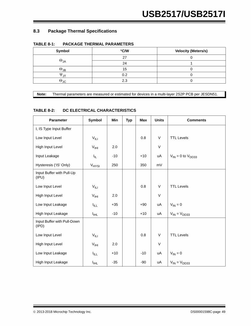
USB2517/USB2517I
8.3 Package Thermal Specifications
TABLE 8-1: PACKAGE THERMAL PARAMETERS
Symbol °C/W Velocity (Meters/s)
JA27 0
24 1
JB 15 0
JT 0.2 0
JC 2.3 0
Note: Thermal parameters are measured or estimated for devices in a multi-layer 2S2P PCB per JESDN51.
TABLE 8-2: DC ELECTRICAL CHARACTERISTICS
Parameter Symbol Min Typ Max Units Comments
I, IS Type Input Buffer
Low Input Level
High Input Level
Input Leakage
Hysteresis (‘IS’ Only)
VILI
VIHI
IIL
VHYSI
2.0
-10
250
0.8
+10
350
V
V
uA
mV
TTL Levels
VIN = 0 to VDD33
Input Buffer with Pull-Up (IPU)
Low Input Level
High Input Level
Low Input Leakage
High Input Leakage
VILI
VIHI
IILL
IIHL
2.0
+35
-10
0.8
+90
+10
V
V
uA
uA
TTL Levels
VIN = 0
VIN = VDD33
Input Buffer with Pull-Down (IPD)
Low Input Level
High Input Level
Low Input Leakage
High Input Leakage
VILI
VIHI
IILL
IIHL
2.0
+10
-35
0.8
-10
-90
V
V
uA
uA
TTL Levels
VIN = 0
VIN = VDD33
2013-2018 Microchip Technology Inc. DS00001598C-page 49
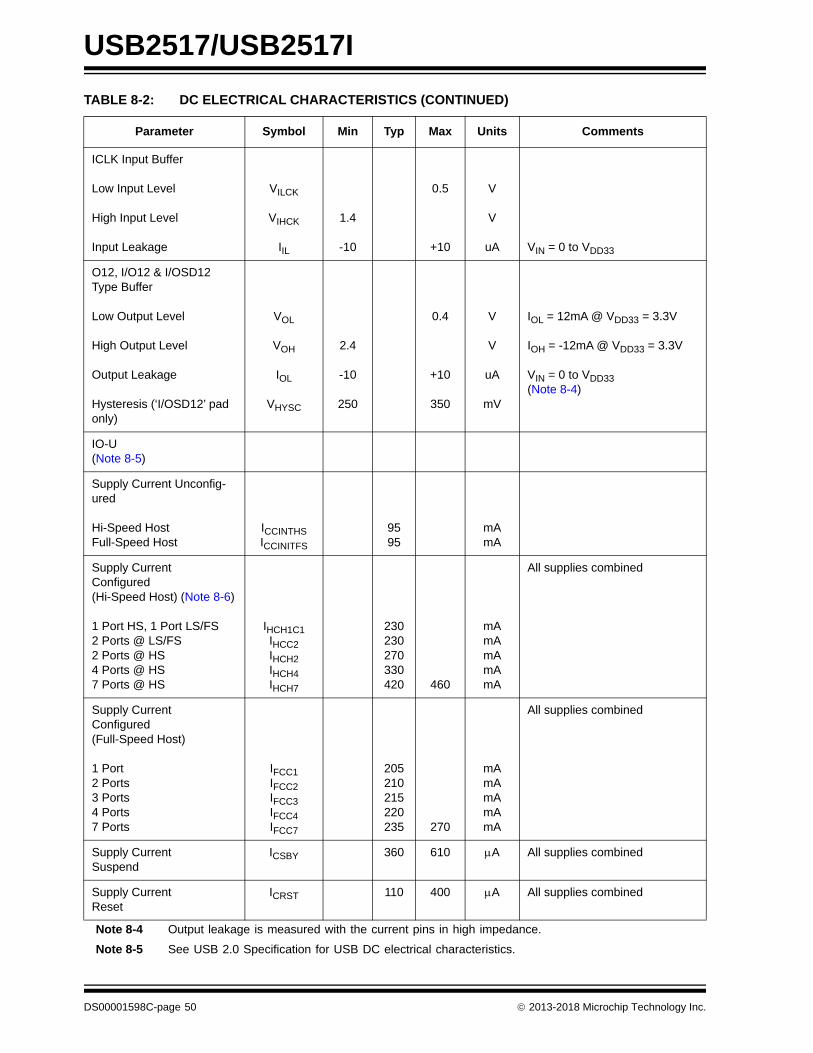
USB2517/USB2517I
Note 8-4 Output leakage is measured with the current pins in high impedance.
Note 8-5 See USB 2.0 Specification for USB DC electrical characteristics.
ICLK Input Buffer
Low Input Level
High Input Level
Input Leakage
VILCK
VIHCK
IIL
1.4
-10
0.5
+10
V
V
uA VIN = 0 to VDD33
O12, I/O12 & I/OSD12 Type Buffer
Low Output Level
High Output Level
Output Leakage
Hysteresis (‘I/OSD12’ pad only)
VOL
VOH
IOL
VHYSC
2.4
-10
250
0.4
+10
350
V
V
uA
mV
IOL = 12mA @ VDD33 = 3.3V
IOH = -12mA @ VDD33 = 3.3V
VIN = 0 to VDD33(Note 8-4)
IO-U(Note 8-5)
Supply Current Unconfig-ured
Hi-Speed HostFull-Speed Host
ICCINTHSICCINITFS
9595
mAmA
Supply Current Configured(Hi-Speed Host) (Note 8-6)
1 Port HS, 1 Port LS/FS2 Ports @ LS/FS2 Ports @ HS4 Ports @ HS7 Ports @ HS
IHCH1C1IHCC2IHCH2IHCH4IHCH7
230230270330420 460
mAmAmAmAmA
All supplies combined
Supply Current Configured(Full-Speed Host)
1 Port 2 Ports3 Ports4 Ports7 Ports
IFCC1IFCC2IFCC3IFCC4IFCC7
205210215220235 270
mAmAmAmAmA
All supplies combined
Supply CurrentSuspend
ICSBY 360 610 A All supplies combined
Supply CurrentReset
ICRST 110 400 A All supplies combined
TABLE 8-2: DC ELECTRICAL CHARACTERISTICS (CONTINUED)
Parameter Symbol Min Typ Max Units Comments
DS00001598C-page 50 2013-2018 Microchip Technology Inc.
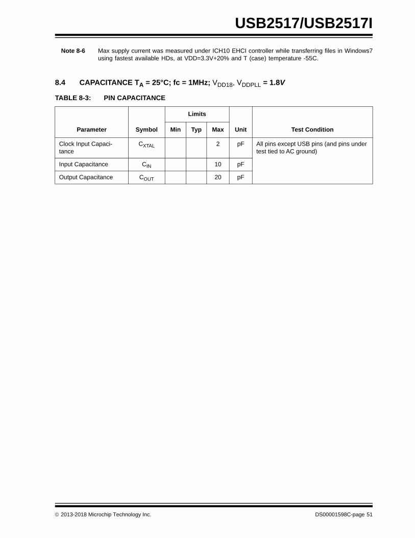
USB2517/USB2517I
Note 8-6 Max supply current was measured under ICH10 EHCI controller while transferring files in Windows7using fastest available HDs, at VDD=3.3V+20% and T (case) temperature -55C.
8.4 CAPACITANCE TA = 25°C; fc = 1MHz; VDD18, VDDPLL = 1.8V
TABLE 8-3: PIN CAPACITANCE
Limits
Parameter Symbol Min Typ Max Unit Test Condition
Clock Input Capaci-tance
CXTAL 2 pF All pins except USB pins (and pins under test tied to AC ground)
Input Capacitance CIN 10 pF
Output Capacitance COUT 20 pF
2013-2018 Microchip Technology Inc. DS00001598C-page 51
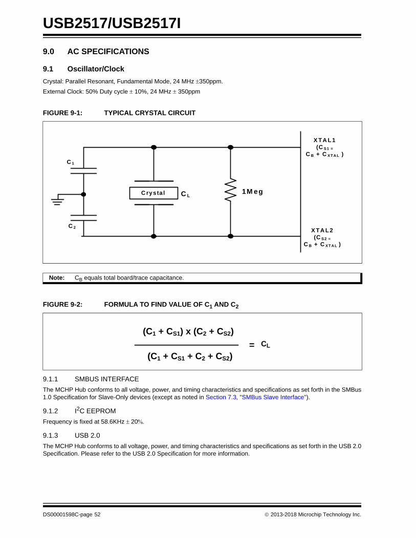
USB2517/USB2517I
DS00001598C-page 52 2013-2018 Microchip Technology Inc.
9.0 AC SPECIFICATIONS
9.1 Oscillator/Clock
Crystal: Parallel Resonant, Fundamental Mode, 24 MHz 350ppm.
External Clock: 50% Duty cycle 10%, 24 MHz 350ppm
9.1.1 SMBUS INTERFACE
The MCHP Hub conforms to all voltage, power, and timing characteristics and specifications as set forth in the SMBus1.0 Specification for Slave-Only devices (except as noted in Section 7.3, "SMBus Slave Interface").
9.1.2 I2C EEPROM
Frequency is fixed at 58.6KHz 20
9.1.3 USB 2.0
The MCHP Hub conforms to all voltage, power, and timing characteristics and specifications as set forth in the USB 2.0Specification. Please refer to the USB 2.0 Specification for more information.
FIGURE 9-1: TYPICAL CRYSTAL CIRCUIT
Note: CB equals total board/trace capacitance.
FIGURE 9-2: FORMULA TO FIND VALUE OF C1 AND C2
X TA L 1(C S 1 =
C B + C X T A L )
X TA L 2(C S 2 =
C B + C X T A L )
C 1
C 2
C L1M egC rysta l
(C1 + CS1) x (C2 + CS2)
(C1 + CS1 + C2 + CS2)
CL=
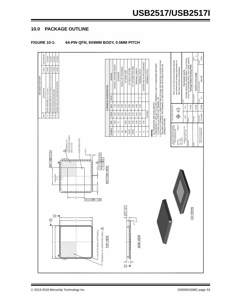
USB2517/USB2517I
10.0 PACKAGE OUTLINE
FIGURE 10-1: 64-PIN QFN, 9X9MM BODY, 0.5MM PITCH
Not
e: F
or th
e m
ost c
urre
nt p
acka
ge d
raw
ings
, se
e th
e M
icro
chip
Pac
kagi
ng S
peci
ficat
ion
at
http
://w
ww
.mic
roch
ip.c
om/p
acka
ging
2013-2018 Microchip Technology Inc. DS00001598C-page 53
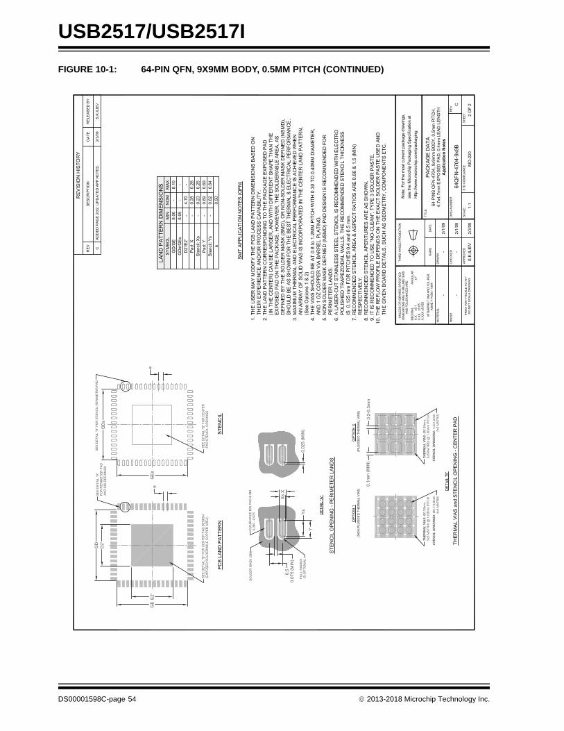
USB2517/USB2517I
FIGURE 10-1: 64-PIN QFN, 9X9MM BODY, 0.5MM PITCH (CONTINUED)
Not
e: F
or th
e m
ost c
urre
nt p
acka
ge d
raw
ings
, se
e th
e M
icro
chip
Pac
kagi
ng S
peci
ficat
ion
at
http
://w
ww
.mic
roch
ip.c
om/p
acka
ging
DS00001598C-page 54 2013-2018 Microchip Technology Inc.
2013-2018 Microchip Technology Inc. DS00001598C-page 55
USB2517/USB2517I
APPENDIX A: DATA SHEET REVISION HISTORY
TABLE A-1: REVISION HISTORY
REVISION LEVEL & DATE SECTION/FIGURE/ENTRY CORRECTION
DS00001598C (04-13-18) Section 8.1, "Maximum Rat-ings"
Section 8.3, "Package Ther-mal Specifications"
Added row: “HBM ESD Performance.
Added section.
DS00001598B (05-23-16) Table 5-1, "USB2517/USB2517I Pin Descriptions"
Corrected the USBDN[7:1]_DP/PRT_DIS_P[7:1] & USBDN[7:1]_DM/PRT_DIS_M[7:1] pin number assign-ments to correctly reflect the 7:1 ordering and clarified the description.
USB2517/USB2517I Rev A, replaces the previous SMSC version, Rev 2.9
USB2517/USB2517I
DS00001598C-page 56 2013-2018 Microchip Technology Inc.
THE MICROCHIP WEB SITE
Microchip provides online support via our WWW site at www.microchip.com. This web site is used as a means to makefiles and information easily available to customers. Accessible by using your favorite Internet browser, the web site con-tains the following information:
• Product Support – Data sheets and errata, application notes and sample programs, design resources, user’s guides and hardware support documents, latest software releases and archived software
• General Technical Support – Frequently Asked Questions (FAQ), technical support requests, online discussion groups, Microchip consultant program member listing
• Business of Microchip – Product selector and ordering guides, latest Microchip press releases, listing of semi-nars and events, listings of Microchip sales offices, distributors and factory representatives
CUSTOMER CHANGE NOTIFICATION SERVICE
Microchip’s customer notification service helps keep customers current on Microchip products. Subscribers will receivee-mail notification whenever there are changes, updates, revisions or errata related to a specified product family ordevelopment tool of interest.
To register, access the Microchip web site at www.microchip.com. Under “Support”, click on “Customer Change Notifi-cation” and follow the registration instructions.
CUSTOMER SUPPORT
Users of Microchip products can receive assistance through several channels:
• Distributor or Representative
• Local Sales Office
• Field Application Engineer (FAE)
• Technical Support
Customers should contact their distributor, representative or field application engineer (FAE) for support. Local salesoffices are also available to help customers. A listing of sales offices and locations is included in the back of this docu-ment.
Technical support is available through the web site at: http://microchip.com/support
2013-2018 Microchip Technology Inc. DS00001598C-page 57
USB2517/USB2517I
PRODUCT IDENTIFICATION SYSTEM
To order or obtain information, e.g., on pricing or delivery, refer to the factory or the listed sales office.
Device: USB2517
Temperature Range:
Blank = 0C to +70C (Commercial)I = -40C to +85C (Industrial)
Package: JZX = 64-pin QFN
Tape and Reel Option:
Blank = Standard packaging (tray)TR = Tape and Reel(1)
Examples:
a) USB2517I - JZX-TRIndustrial temperature,64-pin QFNTape & Reel
b) USB2517-JXZXCommercial temperature,64-pin QFNTray
Note 1: Tape and Reel identifier only appears in the catalog part number description. This identifier is used for ordering purposes and is not printed on the device package. Check with your Microchip Sales Office for package availability with the Tape and Reel option.
PART NO. [X] XXX
PackageTemperatureRange
Device
[X](1)
Tape and ReelOption
- -

USB2517/USB2517I
DS
Note the following details of the code protection feature on Microchip devices:
• Microchip products meet the specification contained in their particular Microchip Data Sheet.
• Microchip believes that its family of products is one of the most secure families of its kind on the market today, when used in the intended manner and under normal conditions.
• There are dishonest and possibly illegal methods used to breach the code protection feature. All of these methods, to our knowledge, require using the Microchip products in a manner outside the operating specifications contained in Microchip’s Data Sheets. Most likely, the person doing so is engaged in theft of intellectual property.
• Microchip is willing to work with the customer who is concerned about the integrity of their code.
• Neither Microchip nor any other semiconductor manufacturer can guarantee the security of their code. Code protection does not mean that we are guaranteeing the product as “unbreakable.”
Code protection is constantly evolving. We at Microchip are committed to continuously improving the code protection features of ourproducts. Attempts to break Microchip’s code protection feature may be a violation of the Digital Millennium Copyright Act. If such actsallow unauthorized access to your software or other copyrighted work, you may have a right to sue for relief under that Act.
Information contained in this publication regarding device applications and the like is provided only for your convenience and may besuperseded by updates. It is your responsibility to ensure that your application meets with your specifications. MICROCHIP MAKES NOREPRESENTATIONS OR WARRANTIES OF ANY KIND WHETHER EXPRESS OR IMPLIED, WRITTEN OR ORAL, STATUTORY OROTHERWISE, RELATED TO THE INFORMATION, INCLUDING BUT NOT LIMITED TO ITS CONDITION, QUALITY, PERFORMANCE,MERCHANTABILITY OR FITNESS FOR PURPOSE. Microchip disclaims all liability arising from this information and its use. Use of Micro-chip devices in life support and/or safety applications is entirely at the buyer’s risk, and the buyer agrees to defend, indemnify and holdharmless Microchip from any and all damages, claims, suits, or expenses resulting from such use. No licenses are conveyed, implicitly orotherwise, under any Microchip intellectual property rights unless otherwise stated.
Trademarks
The Microchip name and logo, the Microchip logo, AnyRate, AVR, AVR logo, AVR Freaks, BeaconThings, BitCloud, CryptoMemory, CryptoRF, dsPIC, FlashFlex, flexPWR, Heldo, JukeBlox, KEELOQ, KEELOQ logo, Kleer, LANCheck, LINK MD, maXStylus, maXTouch, MediaLB, megaAVR, MOST, MOST logo, MPLAB, OptoLyzer, PIC, picoPower, PICSTART, PIC32 logo, Prochip Designer, QTouch, RightTouch, SAM-BA, SpyNIC, SST, SST Logo, SuperFlash, tinyAVR, UNI/O, and XMEGA are registered trademarks of Microchip Technology Incorporated in the U.S.A. and other countries.
ClockWorks, The Embedded Control Solutions Company, EtherSynch, Hyper Speed Control, HyperLight Load, IntelliMOS, mTouch, Precision Edge, and Quiet-Wire are registered trademarks of Microchip Technology Incorporated in the U.S.A.
Adjacent Key Suppression, AKS, Analog-for-the-Digital Age, Any Capacitor, AnyIn, AnyOut, BodyCom, chipKIT, chipKIT logo, CodeGuard, CryptoAuthentication, CryptoCompanion, CryptoController, dsPICDEM, dsPICDEM.net, Dynamic Average Matching, DAM, ECAN, EtherGREEN, In-Circuit Serial Programming, ICSP, Inter-Chip Connectivity, JitterBlocker, KleerNet, KleerNet logo, Mindi, MiWi, motorBench, MPASM, MPF, MPLAB Certified logo, MPLIB, MPLINK, MultiTRAK, NetDetach, Omniscient Code Generation, PICDEM, PICDEM.net, PICkit, PICtail, PureSilicon, QMatrix, RightTouch logo, REAL ICE, Ripple Blocker, SAM-ICE, Serial Quad I/O, SMART-I.S., SQI, SuperSwitcher, SuperSwitcher II, Total Endurance, TSHARC, USBCheck, VariSense, ViewSpan, WiperLock, Wireless DNA, and ZENA are trademarks of Microchip Technology Incorporated in the U.S.A. and other countries.
SQTP is a service mark of Microchip Technology Incorporated in the U.S.A.
Silicon Storage Technology is a registered trademark of Microchip Technology Inc. in other countries.
GestIC is a registered trademark of Microchip Technology Germany II GmbH & Co. KG, a subsidiary of Microchip Technology Inc., in other countries.
All other trademarks mentioned herein are property of their respective companies.
© 2013-2018, Microchip Technology Incorporated, All Rights Reserved.
ISBN: 9781522429029
00001598C-page 58 2013-2018 Microchip Technology Inc.
Microchip received ISO/TS-16949:2009 certification for its worldwide headquarters, design and wafer fabrication facilities in Chandler and Tempe, Arizona; Gresham, Oregon and design centers in California and India. The Company’s quality system processes and procedures are for its PIC® MCUs and dsPIC® DSCs, KEELOQ® code hopping devices, Serial EEPROMs, microperipherals, nonvolatile memory and analog products. In addition, Microchip’s quality system for the design and manufacture of development systems is ISO 9001:2000 certified.
QUALITYMANAGEMENTSYSTEMCERTIFIEDBYDNV
== ISO/TS16949==
DS00001598C-page 59 2013-2018 Microchip Technology Inc.
AMERICASCorporate Office2355 West Chandler Blvd.Chandler, AZ 85224-6199Tel: 480-792-7200 Fax: 480-792-7277Technical Support: http://www.microchip.com/supportWeb Address: www.microchip.com
AtlantaDuluth, GA Tel: 678-957-9614 Fax: 678-957-1455
Austin, TXTel: 512-257-3370
BostonWestborough, MA Tel: 774-760-0087 Fax: 774-760-0088
ChicagoItasca, IL Tel: 630-285-0071 Fax: 630-285-0075
DallasAddison, TX Tel: 972-818-7423 Fax: 972-818-2924
DetroitNovi, MI Tel: 248-848-4000
Houston, TX Tel: 281-894-5983
IndianapolisNoblesville, IN Tel: 317-773-8323Fax: 317-773-5453Tel: 317-536-2380
Los AngelesMission Viejo, CA Tel: 949-462-9523Fax: 949-462-9608Tel: 951-273-7800
Raleigh, NC Tel: 919-844-7510
New York, NY Tel: 631-435-6000
San Jose, CA Tel: 408-735-9110Tel: 408-436-4270
Canada - TorontoTel: 905-695-1980 Fax: 905-695-2078
ASIA/PACIFICAustralia - SydneyTel: 61-2-9868-6733
China - BeijingTel: 86-10-8569-7000
China - ChengduTel: 86-28-8665-5511
China - ChongqingTel: 86-23-8980-9588
China - DongguanTel: 86-769-8702-9880
China - GuangzhouTel: 86-20-8755-8029
China - HangzhouTel: 86-571-8792-8115
China - Hong Kong SARTel: 852-2943-5100
China - NanjingTel: 86-25-8473-2460
China - QingdaoTel: 86-532-8502-7355
China - ShanghaiTel: 86-21-3326-8000
China - ShenyangTel: 86-24-2334-2829
China - ShenzhenTel: 86-755-8864-2200
China - SuzhouTel: 86-186-6233-1526
China - WuhanTel: 86-27-5980-5300
China - XianTel: 86-29-8833-7252
China - XiamenTel: 86-592-2388138
China - ZhuhaiTel: 86-756-3210040
ASIA/PACIFICIndia - BangaloreTel: 91-80-3090-4444
India - New DelhiTel: 91-11-4160-8631
India - PuneTel: 91-20-4121-0141
Japan - OsakaTel: 81-6-6152-7160
Japan - TokyoTel: 81-3-6880- 3770
Korea - DaeguTel: 82-53-744-4301
Korea - SeoulTel: 82-2-554-7200
Malaysia - Kuala LumpurTel: 60-3-7651-7906
Malaysia - PenangTel: 60-4-227-8870
Philippines - ManilaTel: 63-2-634-9065
SingaporeTel: 65-6334-8870
Taiwan - Hsin ChuTel: 886-3-577-8366
Taiwan - KaohsiungTel: 886-7-213-7830
Taiwan - TaipeiTel: 886-2-2508-8600
Thailand - BangkokTel: 66-2-694-1351
Vietnam - Ho Chi MinhTel: 84-28-5448-2100
EUROPEAustria - WelsTel: 43-7242-2244-39Fax: 43-7242-2244-393
Denmark - CopenhagenTel: 45-4450-2828 Fax: 45-4485-2829
Finland - EspooTel: 358-9-4520-820
France - ParisTel: 33-1-69-53-63-20 Fax: 33-1-69-30-90-79
Germany - GarchingTel: 49-8931-9700
Germany - HaanTel: 49-2129-3766400
Germany - HeilbronnTel: 49-7131-67-3636
Germany - KarlsruheTel: 49-721-625370
Germany - MunichTel: 49-89-627-144-0 Fax: 49-89-627-144-44
Germany - RosenheimTel: 49-8031-354-560
Israel - Ra’anana Tel: 972-9-744-7705
Italy - Milan Tel: 39-0331-742611 Fax: 39-0331-466781
Italy - PadovaTel: 39-049-7625286
Netherlands - DrunenTel: 31-416-690399 Fax: 31-416-690340
Norway - TrondheimTel: 47-7289-7561
Poland - WarsawTel: 48-22-3325737
Romania - BucharestTel: 40-21-407-87-50
Spain - MadridTel: 34-91-708-08-90Fax: 34-91-708-08-91
Sweden - GothenbergTel: 46-31-704-60-40
Sweden - StockholmTel: 46-8-5090-4654
UK - WokinghamTel: 44-118-921-5800Fax: 44-118-921-5820
Worldwide Sales and Service
10/25/17