unusual dependence of tc on sample size in superconducting mgb2
TRANSCRIPT

A new method for direct rf power absorption studies in
CMR materials and high Tc superconductors
S. Sarangi and S. V. Bhat*
Department of Physics, Indian Institute of Science, Bangalore – 560012, India
*Corresponding author:
S. V. Bhat
Department of Physics
Indian Institute of Science
Bangalore – 560012, India
Tel.: +91-80-22932727, Fax: +91-80-23602602
E-mail: [email protected]
1

Abstract:
The design, fabrication and performance of an apparatus for the measurement of direct rf
power absorption in colossal magnetoresistive (CMR) and superconducting samples are
described. The system consists of a self-resonant LC tank circuit of an oscillator driven by
a NOT logic gate. The samples under investigation are placed in the core of the coil
forming the inductance L and the absorbed power is determined from the measured
change in the current supplied to the oscillator circuit. A customized low temperature
insert is used to integrate the experiment with a commercial Oxford Instruments cryostat
and temperature controller. The oscillator working in the rf range between 1 MHz to 25
MHz is built around an IC 74LS04. The temperature can be varied from 4.2 to 400 K and
the magnetic field from 0 to 1.4 T. The apparatus is capable of measuring direct power
absorption in CMR and superconducting samples of volume as small as 1 × 10⁻³ cm3 with
a signal to noise ratio of 10:1. Further increase in the sensitivity can be obtained by
summing the results of repeated measurements obtained at a given temperature. The
system performance is evaluated by measuring the absorbed power in La0.7Sr0.3MnO3
(LSMO) CMR manganite samples and superconducting YBa2Cu3O7 (YBCO) samples at
different rf frequencies. All operations during the measurements are automated using a
computer with a menu-driven software system, user input being required only for the
initiation of the measurement sequence.
Keywords: rf absorption; superconductivity; CMR;
2

Introduction:
Recent years have seen the development of two new exciting classes of materials in
condensed matter science, mainly colossal magnetoresistive (CMR) manganites and the
high Tc superconductors. Both of these type of materials are characterized by strongly
correlated electronic systems in them, making the understanding of the phenomena a
challenging task. At the same time they also promise enormous practical applications and
therefore the measurement of their physico-chemical properties is also very important.
From the device applications point of view, one of the crucial parameter is the power
dissipation, especially when subjected to AC fields, which needs to be minimized. It turns
out that both in CMR manganites and high Tc superconductors, the ac losses, especially in
the rf and microwave ranges can have both magnetic and transport contributions. The high
Tc materials are type II superconductors with low Hc1 (lower critical field) values and thus
allow penetration of even low magnetic fields in the form of quantized flux lines. The
motion of these flux lines in response to the induced rf current leads to power dissipation.
In addition, they being intrinsically granular, there is an additional power loss mediated by
the Josephson junctions. In the case of CMR manganites the spin, charge and structural
degrees of freedom are intimately coupled and magnetic and transport properties are
inseparable from each other. While from a theoretical point of view it would be
informative to be able to determine the relative contributions of magnetic and transport
losses separately, for most applications it suffices to determine the absolute and total
magnitude of power dissipation.
3

Different techniques have been used in the past to study the dissipation behavior of high
Tc materials and CMR manganites. One such method especially used for the study of
superconductors are the technique of non-resonant rf power absorption (NRRA) and non
resonant microwave absorption (NRMA). Here conventional CW NMR (Nuclear
Magnetic Resonance) and EPR (Electron Paramagnetic Resonance) spectrometers are
used to record the non resonant response of the sample as a function of temperature and
magnetic field. Magnetic field modulation and phase sensitive detection make this a
highly sensitive electrodeless technique for the characterization of even miniscule a
moment of the samples. However, the main drawback of this technique is its inability to
provide the absolute power loss since only the magnetic field derivative of the absorbed
power (dP/dH) is recorded.
In this work we present a method to measure the absolute power absorbed when either the
CMR or the superconducting sample is subjected to the ac field. We make use of a NOT
logic gate based oscillator, the change in the current supply to which gives a measure of
the absorbed power. Such oscillators have earlier been used [1, 2], but focusing on the
changes in the frequency of the oscillator, which was used to extract information on the
change in the penetration depth and the occurrence of various transitions. As discussed in
the following sections we extend the capability of the technique to include the
measurement of ac dissipation, an important parameter for the characterization of
materials for device applications.
4
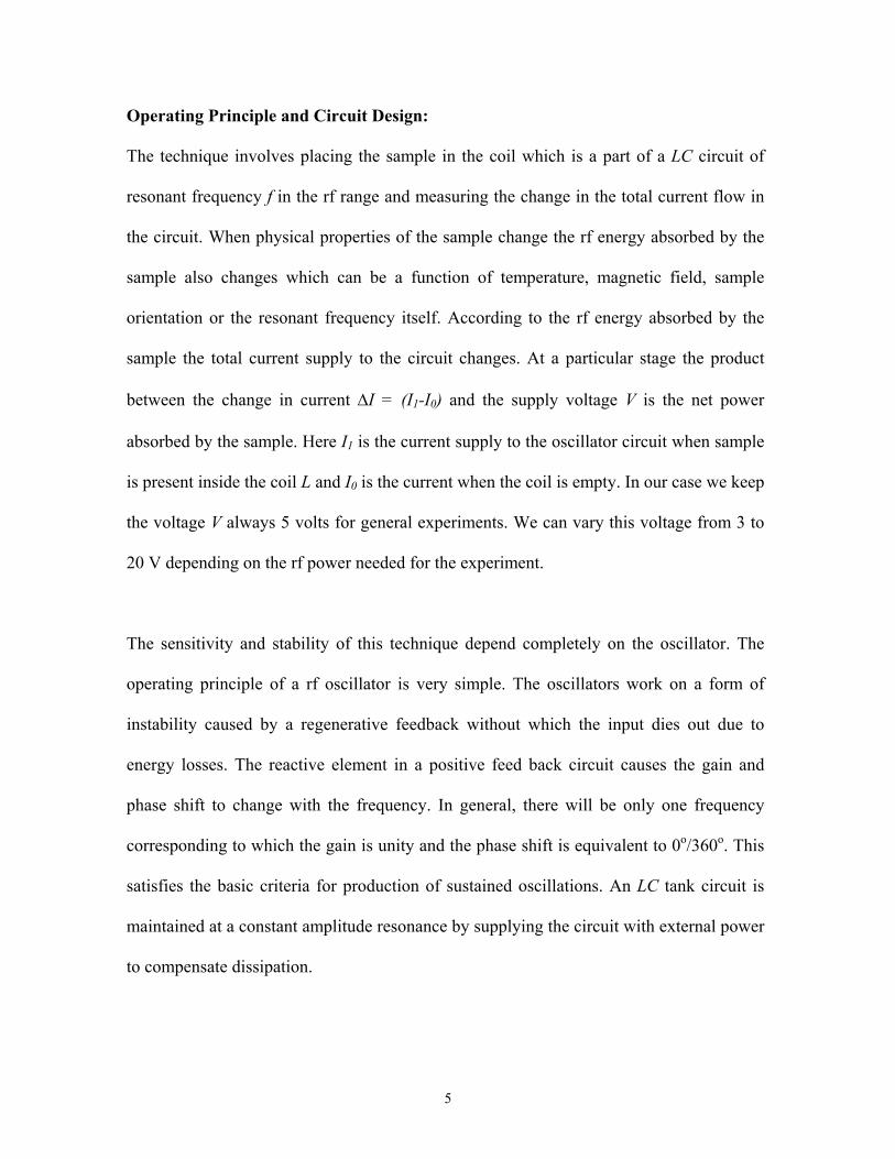
Operating Principle and Circuit Design:
The technique involves placing the sample in the coil which is a part of a LC circuit of
resonant frequency f in the rf range and measuring the change in the total current flow in
the circuit. When physical properties of the sample change the rf energy absorbed by the
sample also changes which can be a function of temperature, magnetic field, sample
orientation or the resonant frequency itself. According to the rf energy absorbed by the
sample the total current supply to the circuit changes. At a particular stage the product
between the change in current ∆I = (I1-I0) and the supply voltage V is the net power
absorbed by the sample. Here I1 is the current supply to the oscillator circuit when sample
is present inside the coil L and I0 is the current when the coil is empty. In our case we keep
the voltage V always 5 volts for general experiments. We can vary this voltage from 3 to
20 V depending on the rf power needed for the experiment.
The sensitivity and stability of this technique depend completely on the oscillator. The
operating principle of a rf oscillator is very simple. The oscillators work on a form of
instability caused by a regenerative feedback without which the input dies out due to
energy losses. The reactive element in a positive feed back circuit causes the gain and
phase shift to change with the frequency. In general, there will be only one frequency
corresponding to which the gain is unity and the phase shift is equivalent to 0o/360o. This
satisfies the basic criteria for production of sustained oscillations. An LC tank circuit is
maintained at a constant amplitude resonance by supplying the circuit with external power
to compensate dissipation.
5

The change in the current is measured with a digital multimeter (Keithley model 2002),
which has DC current measurement sensitivity of 10 pAmp. The fluctuations introduced
due to electrical and thermal noise is taken care of by measuring the mean of 50 data
points. The above measurement can also be done by any sensitive voltmeter. Here we
need to convert the current to voltage by passing the current through a known resistance.
The resistance should be of a low value so that it does not restrict the supply current to the
oscillator. Typically 1 Ω is a good choice for the resistance.
Proper grounding is one of the crucial factors influencing the measurement accuracy. The
best way is to create only one ground point to which all instruments are connected. The
fewer electronics instruments involved in the setup the better, as different instruments
have their own grounds at different potentials. Connection of instruments creates ground
loops and ground loop currents. We recommend using the analogue ground of all the
instruments and not the line ground. As this setup is very sensitive towards ground
problem, it is very important to connect all the metallic part of the cryostat and the helium
dewar also to the same ground.
Fig. 1 shows the oscillator circuit using 74LS04, which is a, TTL bipolar Hex inverter. It
is easily available, cost effective and devoid of any biasing problems. The current in the
inductor and hence the field Hf can be varied by changing the input voltage at pin 14 of
the device. 74LS04 contains six NOT gates with typical propagation delay time ≈ 15 ns.
This specifies the upper limit for its application as a high frequency oscillator. If the
voltage at point “a” is low, then output at 2 (point “b”) is high and the current builds up in
6

the inductor, which in turn transfers its energy to the capacitor. Due to the charging of
capacitor, voltage at “a” develops to high state and output at “b” becomes low and this
leads to sinusoidal oscillations. The frequency of oscillation is determined by series LC
circuit and is given by the standard expression ω=1/(2π√(LC)).
The tank inductance L and capacitance C are vital components of the Integrated circuit
oscillator (ICO) and have to be chosen with utmost care. For C, surface mount high-Q rf
chip capacitor (American Technical Ceramics) with values ranging from 50 to 2000 pF
were tried out. Note that it is important to have the value of C higher than the capacitance
of the 1.5-ft RG402 coaxial assembly, which is rated at 29 pF/ft. The inductive coil is a
15-turn solenoid hand-wound using AWG30 insulated Cu wire around a hollow ceramic
tube (0.8-cm diameter) and potted with polystyrene epoxy resin. A coating of GE varnish
is also applied for good thermal conductivity. Coils with various diameters and wire
thickness were tested for stable performance of the tank circuit. Best results were obtained
for typical inductance value of L=2-9 µH. The output of this circuit is considerable high,
typically .7 V with 5 V input and therefore the circuit can be used for gathering
information on different type of losses.
Low Temperature Cryostat:
The versatility of the experiment is greatly enhanced when it is adapted to conduct
measurements on materials over a wide range in temperature, magnetic field and
frequency. This is achieved in our system through the integration of our home built
circuitry with a customized cryogenic user probe that fits into the commercial Oxford
7

liquid helium cryostat. A semirigid coaxial cable assembly is attached to the probe. The
inductive coil L from the circuit shown in Fig. 1, is connected to the bottom end of the
coaxial cable while the top end is terminated by a female connector that can mated to the
rest of the oscillator circuit. A schematic of the coaxial probe used for the variation in
temperature and magnetic field is shown in Fig. 2.
Samples are placed in gelcaps and inserted into the resonant coil. They are securely
fastened with Teflon tape to ensure rigidity. The sample and coil are in thermal contact
with the temperature sensor (Cernox). Thermal contact is made using Apiezon “N” grease.
The coax is fixed in the central bore of the user probe. A double “O” ring seal at the top
flange (not shown) is used to maintain a vacuum seal around the coax cable. The inner
conductor and the outer shielding are used for electrical connections. Such an arrangement
requires only one cable but the coax must be electrically isolated from the surrounding
environment. Electrical isolation was obtained by wrapping the coax in Teflon tape and
placing a small rubber “O” ring close to the base of the coax. Once the sample and coax
were mounted in the user probe, the probe was then inserted into the cryostat. The Oxford
temperature controller and the Bruker electromagnet are then used as a platform for
varying the sample temperature (4K<T<400K) and static magnetic field (0T<H<1.4T).
Thus, our design combines the ease of operation of the temperature controller (including
the possibility of changing samples without warming up the system) and the static
magnetic field control with the oscillator setup.
8

Computer Interface and Data Acquisition:
Control of the temperature, magnetic field and the frequency was through using the
standard software and a data acquisition computer. Sequences can be written that would
control the temperature and field as a function of time. The analog output ports of a Gauss
meter and Cernox censor were utilized as monitors for the field and temperature. The
signals were then connected to the 2002-multimeter. Here the 2002- multimeter not only
measures the supply current but also measures the DC voltage coming from the Gauss
meter for magnetic field measurement and the resistance of the Cernox censor for
temperature measurement. We use a scanner card for all the measurements in the 2002-
multimeter. It should be noted that this was only used to convert the analog voltage to
general-purpose interface bus (GPIB) readable data. This data is read via GPIB interface
using the same data acquisition computer. The same computer also communicates with the
frequency counter, multimeter, oscilloscope, temperature controller and magnet power
supply unit.
A typical run would scan magnetic field, temperature or frequency over a certain range.
The data acquisition computer would then monitor the GPIB data bus reading
temperature, magnetic field, frequency and the change in current, which is a measure of
the power being absorbed. A schematic of this arrangement is shown in Fig. 3.
System Performance:
Figure 4 shows the output signal trace from the storage oscilloscope with the IC oscillator
at a resonant frequency around 2 MHz. A clean nearly sinusoidal waveform is apparent
9

with peak-to-peak amplitude of around 700 mV. Increasing or decreasing the supply
voltage can adjust the amplitude. If we change the supply voltage from 5 to 10 V the rf
oscillation amplitude changes from 0.7 to 1.4 V. Changing the inductance L of the coil or
the capacitance C of the capacitor changes the resonant frequency.
As mentioned earlier, the experiment depends crucially on the stability of the oscillators.
In Fig. 5 we show the stability of the ICO circuit during a typical magnetic field scan. It is
taken at 200 K by ramping the field in the steps of 10 Gauss up to 1.2 Tesla and back to
zero in 1 hour. The maximum current (45 Amp) corresponds to a dc field of 14 kG for 8.4
cm pole separation. The Fig. 5 also reflects the negligible drift of the oscillations with
time. The 4 micro Amp fluctuation is insignificant compared to the magnitude of the
effects, that is a current shift of 2.5 mAmp at the superconducting transition (Fig. 9) and
120 micro Amp at the CMR transition (Fig 13) in LSMO. Long-term stability tests of the
ICO were conducted and our circuit showed excellent stability. The change due to the drift
in the resonant frequency (~ 1 KHz) is limited to 1 micro amp over a period of 20-30 min.
Tests over a 24 h period established an overall drift around 5 micro amp (Fig. 6).
The temperature dependence shown in Fig. 7 is a combined result of decrease in resistivity
of the Cu wire making up the coil and the effect of thermal contraction, as the temperature
is lowered. In Figure 8 we show the power drift with frequency. The frequency is varied
with only changing C and keeping the amplitude of rf oscillation constant. This shows
very minute change in current with frequency. All the above experiments for system
performance were done in the absence of any samples.
10
It is difficult to track down the precise source for all these drifts as several factors can
contribute. Some possible candidates include drift in the bias supply, IC operation, and
thermal dissipation inside the enclosing Al box. Nevertheless, these small drifts are at
least a few order of magnitudes less than typical current shift encountered in a
measurement and do not affect the result. It must be mentioned, however, that an order of
magnitude improvement in stability can be achieved by giving proper ground to the
metallic part of liquid helium cryostat and the liquid helium dewar.
Both the temperature and field dependence of current shift for the coil are quite repeatable
and not very different for the two cases viz. Coil axis parallel or perpendicular to the dc
field provided by the magnet. As a precaution, it should be noted that if the coil is not
rigidly mounted, one may have to contend with the movement of the coil due to Lorentz
force acting on it when the oscillating rf field (and hence the rf current) is perpendicular to
the applied static field.
Measurements and data collection:
In our first experiment we investigated the high Tc cuprate superconductor YBCO. We
prepared two pellets made of polycrystalline samples of YBCO. Both the pellets were
exactly similar in size but prepared with different techniques. Both the samples show
sharp superconducting transition temperature at ~ 91 K as determined by ρ~T and AC
susceptibility measurements. The material was found to be single phasic as determined by
x-ray diffraction. The samples were placed in the coil. The filling factor of these samples
11

was ~ 0.7. At zero fields the noise in measuring supply current was less than 1 micro
Amp. The superconducting transitions are clearly visible in both the sample (Fig. 9 & Fig.
11) with the background (discussed above) subtracted. One sample (Sample 1) shows the
rf power absorption is less in the superconducting state than the normal state (Fig. 9)
whereas the other sample (Sample 2) shows the power absorption is more in the
superconducting state than the normal state (Fig. 11). Fig. 9 shows that in the normal state
the supply current value is 9.328 mA and superconducting state the supply current is
6.915 mA. From these values we can easily say that in the normal state, the sample #1
absorbs ~12 mW (the product of supply voltage with the change in current) more energy
than its superconducting state. Fig 10 & 12 are the magnetic field dependent power
absorption at various temperatures in both the samples. Here we have plotted the relative
change in current instead of exact value of current just to visualize the change due to field
at different temperature. One sample shows that the rf power absorption increases with
increasing field whereas the other one shows the power absorption decreases with
increasing field. Here it is necessary to note that an increase in current value means that
the rf oscillations are damping very fast and to sustain the oscillations more current has to
be supplied. So more power absorption leads to more supply current to the oscillator. For
sample #1 the power absorption smoothly and monotonically increases with increasing
applied field and shows a tendency to saturate at higher fields. We ascribe this change to
be directly associated with the Joshepson Junction decoupling [13] and fluxon motion [14]
in high Tc superconductors. The shape of the curves and the opposite behavior in these
two samples are associated with flux creep, flux flow, Joshepson Junction critical current,
number density of Joshepson Junctions and the applied frequency. Detailed interpretation
12

of the result and a comparison of preparation techniques which leads to different type of
power absorption are beyond the scope of this instrumentation article and will be
discussed in a forthcoming publication [15].
In our second experiment we investigated with manganite sample. The ICO based NRRA
measurements on the manganite sample, La0.7Sr0.3MnO3 (LSMO), are presented in Fig. 13
and 14. This system was recently synthesized and it’s magnetic and magnetotransport
characteristics were studied at our institute. The sample undergoes a paramagnetic to
ferromagnetic transition as the temperature is lowered with the Curie temperature Tc
around 362 K. In the ICO experiment, the LSMO material is pelletized to capsule form so
that it fits snugly into the core of inductive coil. Figure 13 shows the temperature
dependence of the power absorbed in zero field. Note that the change in the current is
much larger than the background shifts due to empty coil and this has been subtracted in
the data presented in Figs. 13 and 14. The paramagnetic to ferromagnetic transition is
distinctly seen (Fig. 13) and the data are consistent with the existing reports on this
material [16, 17]. In the paramagnetic state the sample absorbs more energy than its
ferromagnetic state. The field dependence for the same sample is plotted in the Fig. 14
where we have shown the data for two cases where the temperature is held above and
below Tc. The striking difference in the current variation in the paramagnetic and the
ferromagnetic phase of the sample is quite obvious. For T>Tc, the current value smoothly
and monotonically decreases with increasing applied field and shows a tendency to
saturate at higher fields. We ascribe this change to be directly associated with the magneto
impedance (MI), which is dominated by rapid change in the permeability. The shape of
13

the curve for T<Tc and the saturation field are different from that seen in the curve for
T>Tc. For T<Tc, the magnetic field dependent power absorption goes through a peak and
then saturates. Detailed interpretation of the results and a comparison of the power
absorption for these systems are beyond the scope of this instrumentation article and will
be discussed in a forthcoming publication [18].
Discussion:
We have demonstrated a contactless method for measuring magnetic and trasport
properties of materials at different temperatures and magnetic fields by using this ICO
based techniques. Many improvements will enhance this ICO method in future. Use of
tunnel diode oscillator in place of IC oscillator would give better stability and resolution.
The technique can be useful for the calculation of ac self-field loss in the rf region.
Preliminary results on CMR and superconducting samples indicate that this instrument
provides a novel way to study the spin and charge dynamics in CMR materials and
Josephson Junctions and vortex phenomena in superconducting materials.
Acknowledgments:
SVB would like to thank CSIR, UGC and DST, India for financial support.
14

References:
[1] H. Srikanth, J. Wiggins, H. Rees, Rev. Sci. Instrum. 70, 3097 (1999).
[2] S. Patnaik, Kanwaljeet Singh, R. C. Budhani, Rev. Sci. Instrum. 70, 1494 (1999).
[3] S.V. Bhat, P. Ganguly, T.V. Ramakrishnan, C.N.R. Rao, J. Phys. C. C20 L559 (1987).
[4] A. Rastogi, Y.S. Sudershan, S.V. Bhat, A.K. Grover, Y. Yamaguchi, K. Oka, Y.
Nishihara, Phys. Rev. B 53 9366 (1996).
[5] G. Blatter, M. V. Feigel’man, V. B. Geshkenbein, A. I. Larkin, V. M. Vinokur, Rev.
Mod. Phys. 66, 1125 (1994).
[6] E. Silva, M. Giura, R. Marcon, R. Fastampa, G. Balestrino, M. Marinelli, E. Milani,
Phys. Rev. B 53 9366 (1996).
[7] J. S. Ramachandran, M. X. Huang, S. M. Bhagat, K. Kish, S. Tyagi, Physica. C 202
151 (1996).
[8] E. M. Jackson, S. B. Liao, J. Silvis, A. H. Swihart, S. M. Bhagat, R. Crittenden, R. E.
Glover III, M. A. Manheimer, Physica. C 152 125 (1988).
[9] R. Marcon, R. Fastampa, M. Giura, E. Silva, Phys. Rev. B 43 2940 (1991).
[10] W. H. Hartwig, C. Passow, Applied Superconductivity, edited by V. L. Newhouse
(Academic, New York, 1975), Vol. II.
[11] R. B. Clover, W. P. Wolf, Rev. Sci. Instrum. 41, 617 (1970).
[12] G. J. Athas, J. S. Brooks, S. J. Klepper, S. Uji, M. Tokumoto, Rev. Sci. Instrum. 64,
3248 (1993).
[13] A. Dulcic, B. Rakvin, M. Pozek, Europhys. Lett. 10. 593 (1989).
[14] A.M. Portis, K.W. Blazey, K.A. Muller, J.G. Bednorz, Europhys. Lett. 5. 467-472
(1988).
15

[15] S. Sarangi, S. P. Chockalingam, S. V. Bhat (to be published).
[16] S. Y. Yang, W. L. Kuang, Y. Liou, W. S. Tse, S. F. Lee, Y. D. Yao, Journal of
Magnetism and Magnetic Materials. 268 (2004) 326-331.
[17] A. K. Debnath, J. G. Lin, Phys. Rev. B 67, 064412 (2003).
[18] S. Sarangi, S. S. Rao, S. V. Bhat (to be published).
16

Figure Legends:
1. RF oscillator circuit with IC 74LS04.
2. Schematic of the low temperature probe showing the sample region.
3. Layout of the complete ICO measurement system displaying computer control and
data acquisition stages.
4. The output waveform from the ICO circuit measured with a digital oscilloscope. The
resonant frequency is around 2 MHz.
5. The Current passing in the circuit at 200 K plotted against magnetic field for the
empty coil. The duration of field scan is 1 h.
6. The current passing in the circuit against time when the coil is empty. This is a full
day experiment.
7. The current as a function of temperature for the empty coil.
8. The current passing in the circuit at room temperature against resonant frequency of
the oscillator.
9. Measured zero-field temperature dependence of the current for the YBCO (sample 1).
The critical temperature Tc is 91 K.
10. Field dependence of current for the YBCO (sample 1) above and below the critical
temperature Tc. The magnetic field is scanned from –150 Gauss to +150 Gauss in 60
seconds.
11. Measured zero-field temperature dependence of the current for the YBCO (sample 2).
The critical temperature Tc is 91 K.
17

12. Field dependence of current for the YBCO (sample 2) above and below the critical
temperature Tc. The magnetic field is scanned from –150 Gauss to +150 Gauss in 60
seconds.
13. Measured zero-field temperature dependence of the current for the LSMO sample. The
paramagnetic to ferromagnetic transition at 362 K.
14. Field dependence of current for the LSMO sample above and below the ferromagnetic
transition temperature Tc. The magnetic field is scanned from –150 Gauss to +150 Gauss
in 60 seconds.
18

FIG. 1
19

FIG. 2
20

FIG. 3
21

FIG. 4
22

FIG. 5
23
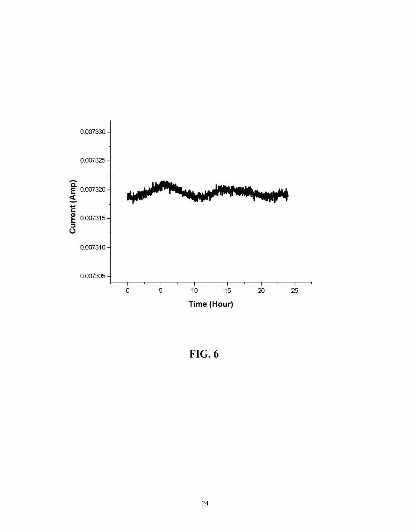
FIG. 6
24

FIG. 7
25

FIG. 8
26

FIG. 9
27

FIG. 10
28

FIG. 11
29

FIG. 12
30

FIG. 13
31

FIG. 14
32